arm versatile express cortex -m prototyping system (v2m-mps2) · about this book this book...
TRANSCRIPT

ARM® Versatile™ Express Cortex®-MPrototyping System (V2M-MPS2)
Technical Reference Manual
Copyright © 2013-2015 ARM. All rights reserved.ARM 100112_0100_03_en

ARM® Versatile™ Express Cortex®-M Prototyping System (V2M-MPS2)Technical Reference ManualCopyright © 2013-2015 ARM. All rights reserved.
Release Information
Document History
Issue Date Confidentiality Change
DDI0525A 20 December 2013 Non-Confidential First release for V2M-MPS2 TRM
DDI0525B 1 October 2014 Non-Confidential Second release for V2M-MPS2 TRM
DDI0525C 10 November 2014 Non-Confidential Third release for V2M-MPS2 TRM
0100-03 02 April 2015 Non-Confidential Fourth release for V2M-MPS2 TRM
Non-Confidential Proprietary Notice
This document is protected by copyright and other related rights and the practice or implementation of the information contained inthis document may be protected by one or more patents or pending patent applications. No part of this document may bereproduced in any form by any means without the express prior written permission of ARM. No license, express or implied, byestoppel or otherwise to any intellectual property rights is granted by this document unless specifically stated.
Your access to the information in this document is conditional upon your acceptance that you will not use or permit others to usethe information for the purposes of determining whether implementations infringe any third party patents.
THIS DOCUMENT IS PROVIDED “AS IS”. ARM PROVIDES NO REPRESENTATIONS AND NO WARRANTIES,EXPRESS, IMPLIED OR STATUTORY, INCLUDING, WITHOUT LIMITATION, THE IMPLIED WARRANTIES OFMERCHANTABILITY, SATISFACTORY QUALITY, NON-INFRINGEMENT OR FITNESS FOR A PARTICULAR PURPOSEWITH RESPECT TO THE DOCUMENT. For the avoidance of doubt, ARM makes no representation with respect to, and hasundertaken no analysis to identify or understand the scope and content of, third party patents, copyrights, trade secrets, or otherrights.
This document may include technical inaccuracies or typographical errors.
TO THE EXTENT NOT PROHIBITED BY LAW, IN NO EVENT WILL ARM BE LIABLE FOR ANY DAMAGES,INCLUDING WITHOUT LIMITATION ANY DIRECT, INDIRECT, SPECIAL, INCIDENTAL, PUNITIVE, ORCONSEQUENTIAL DAMAGES, HOWEVER CAUSED AND REGARDLESS OF THE THEORY OF LIABILITY, ARISINGOUT OF ANY USE OF THIS DOCUMENT, EVEN IF ARM HAS BEEN ADVISED OF THE POSSIBILITY OF SUCHDAMAGES.
This document consists solely of commercial items. You shall be responsible for ensuring that any use, duplication or disclosure ofthis document complies fully with any relevant export laws and regulations to assure that this document or any portion thereof isnot exported, directly or indirectly, in violation of such export laws. Use of the word “partner” in reference to ARM’s customers isnot intended to create or refer to any partnership relationship with any other company. ARM may make changes to this document atany time and without notice.
If any of the provisions contained in these terms conflict with any of the provisions of any signed written agreement covering thisdocument with ARM, then the signed written agreement prevails over and supersedes the conflicting provisions of these terms.This document may be translated into other languages for convenience, and you agree that if there is any conflict between theEnglish version of this document and any translation, the terms of the English version of the Agreement shall prevail.
Words and logos marked with ® or ™ are registered trademarks or trademarks of ARM Limited or its affiliates in the EU and/orelsewhere. All rights reserved. Other brands and names mentioned in this document may be the trademarks of their respectiveowners. Please follow ARM’s trademark usage guidelines at http://www.arm.com/about/trademark-usage-guidelines.php
Copyright © [2013-2015], ARM Limited or its affiliates. All rights reserved.
ARM Limited. Company 02557590 registered in England.
110 Fulbourn Road, Cambridge, England CB1 9NJ.
LES-PRE-20349
ARM® Versatile™ Express Cortex®-M Prototyping System (V2M-MPS2)
ARM 100112_0100_03_en Copyright © 2013-2015 ARM. All rights reserved. 2Non-Confidential

Confidentiality Status
This document is Non-Confidential. The right to use, copy and disclose this document may be subject to license restrictions inaccordance with the terms of the agreement entered into by ARM and the party that ARM delivered this document to.
Unrestricted Access is an ARM internal classification.
Product Status
The information in this document is Final, that is for a developed product.
Web Address
http://www.arm.com
Conformance Notices
Federal Communications Commission NoticeThis device is test equipment and consequently is exempt from part 15 of the FCC Rules under section 15.103 (c).
CE Declaration of Conformity
The system should be powered down when not in use.
It is recommended that ESD precautions be taken when handling Versatile™ Express boards.
The motherboard generates, uses, and can radiate radio frequency energy and may cause harmful interference to radiocommunications. There is no guarantee that interference will not occur in a particular installation. If this equipment causes harmfulinterference to radio or television reception, which can be determined by turning the equipment off or on, you are encouraged to tryto correct the interference by one or more of the following measures:
• Ensure attached cables do not lie across the target board• Reorient the receiving antenna• Increase the distance between the equipment and the receiver• Connect the equipment into an outlet on a circuit different from that to which the receiver is connected• Consult the dealer or an experienced radio/TV technician for help
Note
It is recommended that wherever possible shielded interface cables be used.
ARM® Versatile™ Express Cortex®-M Prototyping System (V2M-MPS2)
ARM 100112_0100_03_en Copyright © 2013-2015 ARM. All rights reserved. 3Non-Confidential

ContentsARM® Versatile™ Express Cortex®-M PrototypingSystem (V2M-MPS2) Technical Reference Manual
PrefaceAbout this book ...................................................... ...................................................... 7Feedback .................................................................................................................... 10
Chapter 1 Introduction1.1 Precautions .............................................................................................................. 1-121.2 About the Versatile™ Express V2M-MPS2 motherboard .......................................... 1-131.3 Location of components on the V2M-MPS2 motherboard ................... ................... 1-14
Chapter 2 Hardware Description2.1 Overview of the V2M-MPS2 motherboard hardware ....................... ....................... 2-182.2 Clocks ...................................................................................................................... 2-212.3 Powerup, powerdown and resets ...................................... ...................................... 2-232.4 User expansion port ................................................ ................................................ 2-242.5 USB 2.0 Full Speed interface ......................................... ......................................... 2-252.6 SPI interface ............................................................................................................ 2-262.7 UART interface ........................................................................................................ 2-272.8 VGA and CLCD interfaces ........................................... ........................................... 2-282.9 Audio interface .................................................... .................................................... 2-292.10 Ethernet interface .................................................. .................................................. 2-302.11 User switches and user LEDs ........................................ ........................................ 2-312.12 External user memory .............................................. .............................................. 2-32
ARM 100112_0100_03_en Copyright © 2013-2015 ARM. All rights reserved. 4Non-Confidential
2.13 MCC FPGA serial interface .......................................... .......................................... 2-352.14 Power ........................................................... ........................................................... 2-382.15 Debug and trace ...................................................................................................... 2-392.16 Minimum design settings for motherboard operation ....................... ....................... 2-43
Chapter 3 Configuration3.1 Overview of the V2M-MPS2 motherboard configuration process ............................ 3-453.2 Configuration system ............................................... ............................................... 3-473.3 Powerup and configuration process .................................... .................................... 3-483.4 Reset push buttons .................................................................................................. 3-503.5 Configuration files .................................................................................................... 3-51
Chapter 4 Programmers Model4.1 About this programmers model ....................................... ....................................... 4-554.2 Memory map ............................................................................................................ 4-564.3 Register summary ................................................. ................................................. 4-574.4 SCC register descriptions ........................................................................................ 4-584.5 System configuration registers ........................................ ........................................ 4-65
Chapter 5 Signal Descriptions5.1 Debug connectors ................................................. ................................................. 5-705.2 Expansion connectors .............................................. .............................................. 5-755.3 CLCD connector ...................................................................................................... 5-775.4 USB 2.0 connector ................................................. ................................................. 5-785.5 UART connector ...................................................................................................... 5-795.6 SPI connector .......................................................................................................... 5-805.7 VGA connector .................................................... .................................................... 5-815.8 Audio connectors .................................................. .................................................. 5-825.9 Ethernet connector ................................................. ................................................. 5-835.10 12V power connector ............................................... ............................................... 5-84
Appendix A.1 SpecificationsA.1.1 Electrical specification ......................................... ......................................... Appx-A-86
Appendix B.2 RevisionsB.2.1 Revisions ................................................... ................................................... Appx-B-88
ARM 100112_0100_03_en Copyright © 2013-2015 ARM. All rights reserved. 5Non-Confidential

Preface
This preface introduces the ARM® Versatile™ Express Cortex®-M Prototyping System (V2M-MPS2)Technical Reference Manual.
It contains the following:• About this book on page 7.• Feedback on page 10.
ARM 100112_0100_03_en Copyright © 2013-2015 ARM. All rights reserved. 6Non-Confidential

About this bookThis book describes the ARM® Versatile™ Express Cortex®-M Prototyping System, that is, the V2M-MPS2 motherboard. Previous issues of this book had document number DDI0525.
Product revision status
The rmpn identifier indicates the revision status of the product described in this book, for example, r1p2,where:
rm Identifies the major revision of the product, for example, r1.pn Identifies the minor revision or modification status of the product, for example, p2.
Intended audience
This book is written for experienced hardware and software engineers who are doing ARM M-Classprocessor evaluation and development using the Versatile™ Express Cortex®-M Prototyping System, theV2M-MPS2 motherboard.
Using this book
This book is organized into the following chapters:
Chapter 1 IntroductionThis chapter provides an introduction to the Versatile Express Cortex-M Prototyping System, theV2M-MPS2 motherboard.
Chapter 2 Hardware DescriptionThis chapter describes the Versatile Express V2M-MPS2 motherboard hardware.
Chapter 3 ConfigurationThis chapter describes the powerup and configuration process of the Versatile Express V2M-MPS2 motherboard.
Chapter 4 Programmers ModelThis chapter describes the programmers model of the Versatile Express V2M-MPS2 motherboard.
Chapter 5 Signal DescriptionsThis chapter describes the signals present at the interface connectors of the Versatile ExpressV2M-MPS2 motherboard
Appendix A.1 SpecificationsThis chapter contains the electrical specification of the Versatile Express V2M-MPS2motherboard and FPGA.
Appendix B.2 RevisionsThis chapter describes the technical changes between released issues of this book.
Glossary
The ARM Glossary is a list of terms used in ARM documentation, together with definitions for thoseterms. The ARM Glossary does not contain terms that are industry standard unless the ARM meaningdiffers from the generally accepted meaning.
See the ARM Glossary for more information.
Typographic conventions
italicIntroduces special terminology, denotes cross-references, and citations.
boldHighlights interface elements, such as menu names. Denotes signal names. Also used for termsin descriptive lists, where appropriate.
Preface About this book
ARM 100112_0100_03_en Copyright © 2013-2015 ARM. All rights reserved. 7Non-Confidential

monospaceDenotes text that you can enter at the keyboard, such as commands, file and program names,and source code.
monospaceDenotes a permitted abbreviation for a command or option. You can enter the underlined textinstead of the full command or option name.
monospace italicDenotes arguments to monospace text where the argument is to be replaced by a specific value.
monospace boldDenotes language keywords when used outside example code.
<and>Encloses replaceable terms for assembler syntax where they appear in code or code fragments.For example:
MRC p15, 0, <Rd>, <CRn>, <CRm>, <Opcode_2>
SMALL CAPITALS
Used in body text for a few terms that have specific technical meanings, that are defined in theARM glossary. For example, IMPLEMENTATION DEFINED, IMPLEMENTATION SPECIFIC, UNKNOWN, andUNPREDICTABLE.
Timing diagrams
The following figure explains the components used in timing diagrams. Variations, when they occur,have clear labels. You must not assume any timing information that is not explicit in the diagrams.
Shaded bus and signal areas are undefined, so the bus or signal can assume any value within the shadedarea at that time. The actual level is unimportant and does not affect normal operation.
Clock
HIGH to LOW
Transient
HIGH/LOW to HIGH
Bus stable
Bus to high impedance
Bus change
High impedance to stable bus
Figure 1 Key to timing diagram conventions
Signals
The signal conventions are:
Signal levelThe level of an asserted signal depends on whether the signal is active-HIGH or active-LOW.Asserted means:• HIGH for active-HIGH signals.• LOW for active-LOW signals.
Lower-case nAt the start or end of a signal name denotes an active-LOW signal.
Additional reading
This book contains information that is specific to this product. See the following documents for otherrelevant information.
Preface About this book
ARM 100112_0100_03_en Copyright © 2013-2015 ARM. All rights reserved. 8Non-Confidential

ARM publications• Cortex®-M0+ Technical Reference Manual (ARM DDI 0484)• Cortex®-M0 Technical Reference Manual (ARM DDI 0432)• Cortex®-M1 FPGA Development Kit Cortex-M1 User Guide: Altera Edition v1.1 (ARM DUI
0395)• Cortex®-M1 FPGA Development Kit v1.1: Installation Guide (ARM DSI 0048)• Cortex®-M1 Technical Reference Manual (ARM DDI 0413)• Cortex®-M3 Technical Reference Manual (ARM DDI 0337)• Cortex®-M3 Devices Generic User Guide (ARM DUI 0552)• Cortex®-M4 Technical Reference Manual (ARM DDI 0439)• Cortex®-M4 Devices Generic User Guide (ARM DUI 0553)• Cortex®-M System Design Kit Technical Reference Manual (ARM DDI 0479)• Application Note AN382 ARM® Cortex®-M0 SMM on V2M_MPS2 (ARM DAI 0382)• Application Note AN383 ARM® Cortex®-M0+ SMM on V2M-MPS2 (ARM DAI 0383)• Application Note AN384 ARM® Cortex®-M1 SMM on V2M-MPS2 (ARM DAI 0384)• Application Note AN385 ARM® Cortex®-M3 SMM on V2M-MPS2 (ARM DAI 0385)• Application Note AN386 ARM® Cortex®-M4 SMM on V2M-MPS2 (ARM DAI 0386)• Application Note AN387 ARM® Cortex®-M0 Design Start SMM on V2M-MPS2 (ARM DAI
0387)• Application Note AN399 ARM® Cortex®-M7 SMM on V2M-MPS2 (ARM DAI 0399)• Application Note AN400 ARM® Cortex®-M7CS SMM on V2M-MPS2 (ARM DAI 0400)• Cortex®-M1 FPGA Development Kit Example System Tutorial: Altera Cyclone III Edition
(ARM DUI 0430)• ARM DSTREAM System and Interface Design Reference (ARM DUI 0499)• ARM DSTREAM Setting up the Hardware (ARM DUI 0481)• ARM DSTREAM and RVI Using the Debug Hardware Configuration Utilities (ARM DUI
0498)• ARM CoreSight™ Components Technical Reference Manual (ARM DDI 0314)
Other publications• See the Altera website http://altera.com for information on the Altera Cyclone 5CEA7
FPGA.
Preface About this book
ARM 100112_0100_03_en Copyright © 2013-2015 ARM. All rights reserved. 9Non-Confidential

Feedback
Feedback on this product
If you have any comments or suggestions about this product, contact your supplier and give:• The product name.• The product revision or version.• An explanation with as much information as you can provide. Include symptoms and diagnostic
procedures if appropriate.
Feedback on content
If you have comments on content then send an e-mail to [email protected]. Give:
• The title ARM® Versatile™ Express Cortex®-M Prototyping System (V2M-MPS2) TechnicalReference Manual.
• The number ARM 100112_0100_03_en.• If applicable, the page number(s) to which your comments refer.• A concise explanation of your comments.
ARM also welcomes general suggestions for additions and improvements. Note
ARM tests the PDF only in Adobe Acrobat and Acrobat Reader, and cannot guarantee the quality of therepresented document when used with any other PDF reader.
Preface Feedback
ARM 100112_0100_03_en Copyright © 2013-2015 ARM. All rights reserved. 10Non-Confidential

Chapter 1Introduction
This chapter provides an introduction to the Versatile Express Cortex-M Prototyping System, the V2M-MPS2 motherboard.
It contains the following sections:• 1.1 Precautions on page 1-12.• 1.2 About the Versatile™ Express V2M-MPS2 motherboard on page 1-13.• 1.3 Location of components on the V2M-MPS2 motherboard on page 1-14.
ARM 100112_0100_03_en Copyright © 2013-2015 ARM. All rights reserved. 1-11Non-Confidential

1.1 PrecautionsThis section contains advice about how to prevent damage to your .
This section contains the following subsections:• 1.1.1 Ensuring safety on page 1-12.• 1.1.2 Preventing damage on page 1-12.
1.1.1 Ensuring safety
An on-board connector supplies 12V DC to the Cortex-M Prototyping System.
Warning
Do not use the Cortex-M Prototyping System near equipment that is sensistive to electromagneticemissions, for example, medical equipment.
1.1.2 Preventing damage
The Cortex Prototyping System is intended for use within a laboratory or engineering developmentenvironment. The board is sensitive to electrostatic discharges and permits electromagnetic emissions.
Caution
To avoid damage to the Cortex Prototyping System, observe the following precautions:• You must connect the external power supply to the board before powerup to prevent damage.• Never subject the board to high electrostatic potentials. Observe Electrostatic Discharge (ESD)
precautions when handling any board.• Always wear a grounding strap when handling the board.• Only hold the board by the edges.• Avoid touching the component pins or any other metallic element except the metal shielding for the
connectors.• Avoid contact with components on the board which may be hot or sharp.• Ensure that the voltage on the pins of the FPGA and interface circuitry on the board is at the correct
level.• You must not configure as outputs any FPGA pins that connect directly to other outputs or an external
signal source.• Do not use the board near a transmitter of electromagnetic emissions.
1 Introduction1.1 Precautions
ARM 100112_0100_03_en Copyright © 2013-2015 ARM. All rights reserved. 1-12Non-Confidential
1.2 About the Versatile™ Express V2M-MPS2 motherboardThe V2M-MPS2 motherboard is a development platform for ARM Cortex-M evaluation anddevelopment.
The V2M-MPS2 motherboard provides the following:
Altera Cyclone 5CEA7 FPGA and board powerup and configurationThe V2M-MPS2 motherboard provides an Altera Cyclone 5CEA7 FPGA, speed grade C8, thatsupports ARM Cortex-M software evaluation and development. A Motherboard ConfigurationController (MCC) supports board powerup and configuration. An on-board EEPROM storesboard and file identification information and a microSD card stores FPGA and software imagesand configuration files. You can access the microSD card to perform configuration file editingand to update FPGA and software images.
External user memoryOn-board external SSRAM and PSRAM connect to memory interfaces in the FPGA.
Access portsThe V2M-MPS2 motherboard provides access through Ethernet, general-purpose UART andSPI ports. A general-purpose user expansion port supports user expansion to extra signal or busIO.
Video and audio outputThe V2M-MPS2 motherboard provides video output through VGA and CLCD ports. The CLCDport drives an LCD module configured for SPI graphics and I2C touch screen. Input and outputaudio ports connect to a stereo audio codec which connects to an I2S digital audio interface onthe FPGA.
User LEDs and user switchesThe V2M-MPS2 motherboard provides user LEDs, an 8-way dip switch and push buttons thatconnect to the FPGA and to the MCC. The meaning of these LEDs and push buttons dependupon the image that you implement in the FPGA.
System LEDsThe V2M-MPS2 motherboard provides LEDs which denote Configuration Complete, MCCPowered, Ethernet Duplex Link Established, Ethernet Link Operating at 100Mbs, Ethernet LinkEstablished and microSD Card Read or Write Access.
DebugThe V2M-MPS2 motherboard supports P-JTAG Processor debug, F-JTAG Integrated LogicAnalyzer (ILA) FPGA debug, 4-bit trace and 16-bit trace debug, and CMSIS-DAP FPGA debug.
Note
The V2M-MPS2 motherboard requires motherboard configuration controller firmware version2.0.1 or later to support CMSIS-DAP FPGA debug.
1 Introduction1.2 About the Versatile™ Express V2M-MPS2 motherboard
ARM 100112_0100_03_en Copyright © 2013-2015 ARM. All rights reserved. 1-13Non-Confidential

1.3 Location of components on the V2M-MPS2 motherboardThe following figure shows the upper face of the V2M-MPS2 motherboard.
1 Introduction1.3 Location of components on the V2M-MPS2 motherboard
ARM 100112_0100_03_en Copyright © 2013-2015 ARM. All rights reserved. 1-14Non-Confidential

Expansion connector
EXP2
Expansion connector
EXP1
LCD display panel
2MB ZBT SSRAM
12V DCpower jack
RJ45Ethernet
connectorOut
VGA General purpose UART
Stereo line audio
JTAG 14
ARM JTAG 20
MICTOR 38
CORESIGHT 20
CORESIGHT 10Reserved
MCC
PSRAM8MB
ON/OFF soft RESET push button
Hardware RESET
push button
MCC user LEDs
FPGA user push buttons
PB0PB1
SPI header
In
Altera Cyclone 5CEA7 FPGA
MCC user switches
Clock connection
headers and slide switches
J22
J23
J18
J19
Ethernet activity LEDs DPLX
LINK100Mbs
USB 2.0configuration
port
FPGA user
LED 1
1
8765432
HDDPWR
DONE
System LEDs1
8765432
FPGA user
LED 0
3V battery
Figure 1-1 Upper face of the V2M-MPS2 motherboard.
The following figure shows the lower face of the V2M-MPS2 motherboard.
1 Introduction1.3 Location of components on the V2M-MPS2 motherboard
ARM 100112_0100_03_en Copyright © 2013-2015 ARM. All rights reserved. 1-15Non-Confidential

2MB ZBT SSRAM
2MB ZBT SSRAM
microSDCard
Figure 1-2 Lower face of the V2M-MPS2 motherboard.
1 Introduction1.3 Location of components on the V2M-MPS2 motherboard
ARM 100112_0100_03_en Copyright © 2013-2015 ARM. All rights reserved. 1-16Non-Confidential

Chapter 2Hardware Description
This chapter describes the Versatile Express V2M-MPS2 motherboard hardware.
It contains the following sections:• 2.1 Overview of the V2M-MPS2 motherboard hardware on page 2-18.• 2.2 Clocks on page 2-21.• 2.3 Powerup, powerdown and resets on page 2-23.• 2.4 User expansion port on page 2-24.• 2.5 USB 2.0 Full Speed interface on page 2-25.• 2.6 SPI interface on page 2-26.• 2.7 UART interface on page 2-27.• 2.8 VGA and CLCD interfaces on page 2-28.• 2.9 Audio interface on page 2-29.• 2.10 Ethernet interface on page 2-30.• 2.11 User switches and user LEDs on page 2-31.• 2.12 External user memory on page 2-32.• 2.13 MCC FPGA serial interface on page 2-35.• 2.14 Power on page 2-38.• 2.15 Debug and trace on page 2-39.• 2.16 Minimum design settings for motherboard operation on page 2-43.
ARM 100112_0100_03_en Copyright © 2013-2015 ARM. All rights reserved. 2-17Non-Confidential

2.1 Overview of the V2M-MPS2 motherboard hardwareThe hardware infrastructure supports ARM M-class processor evaluation and development, systemexpansion and a number of debug interfaces.
The following figure shows the high-level hardware infrastructure.
Note
The image that the configuration systems loads into the FPGA at powerup defines the functionality of theV2M-MPS2 motherboard.
Versatile Express V2M-MPS2
Clock generators
FPGA
ZBT SSRAM 1 2MB
32-bit
32-bit
User push buttons
LEDs
microSD card(USBMSD)
ConfigurationEEPROM
JTAG 14
UART
VGA
ETHERNET
EXP[51:26]
USB 2.0ZBT SSRAM 2
2MB
PSRAM 18MB
ZBT SSRAM 3 2MB
Expansion
CLCD
MCC
MAC/PHY
DIP switches
LEDs
EXP[25:0]
Stereo audio codec
Audio Audio
CLCD
F-JTAG
CoreSight 10
CoreSight 20
MICTOR 38 P-JTAG/SWD16-bit Trace
SCC
VGA
Configuration
ON/OFF/Soft RESET push button
Hardware RESET push button
P-JTAG/SWD4-bit Trace
4-bit Trace16-bit Trace
I2C I2Saudio
SPISPI
Expansion
ZBT SSRAM 1 2MB64-bit
PSRAM 08MB
16-bit
32-bit
32-bit
ARM JTAG 20 P-JTAG/SWDP-JTAG/SWD
P-JTAG/SWD
CMSIS-DAP
3V battery
Real Time Clock
Figure 2-1 V2M-MPS2 motherboard hardware infrastructure
2 Hardware Description2.1 Overview of the V2M-MPS2 motherboard hardware
ARM 100112_0100_03_en Copyright © 2013-2015 ARM. All rights reserved. 2-18Non-Confidential

The V2M-MPS2 motherboard contains the following components and interfaces:• One Altera Cyclone 5CEA7 FPGA:
— speed grade C8.• External user system memory for Cortex-M processors:
— Two 32-bit 2MB ZBT SSRAM with independent 32-bit memory interfaces.— One 64-bit 4MB ZBT SSRAM:
◦ Two 32-bit 2MB ZBT SSRAM connected as one 4MB 64-bit memory.— Two 16-bit 8MB PSRAM to supplement ZBT SSRAM.
• One MCC that supports board configuration at powerup or reset:— FPGA configuration.— Clock generator configuration.— Board configuration.— Pre-loading of SRAM images.— Loading of Real Time Clock (RTCC) registers.— CMSIS-DAP FPGA debug through the USB 2.0 port.
• One microSD card that stores the following:— FPGA images.— Software images.— Board configuration files.
• On-board clock generators:— One fixed 25MHz clock for Ethernet MAC/PHY.— Three programmable system clocks.— Two crystals for MCC.
• Real Time Clock (RTC) in MCC:— Powered by 3V lithium coin cell battery.
• I2S digital audio output:• IDC expansion ports:• Ethernet port.• UART.• SPI interface.• Video output:
— VGA output.— CLCD output with SPI interface.
• USB 2.0 Full Speed port that supports:— USB memory access to the microSD card for Drag-and-Drop configuration file editing.
• User switches and user LEDs:— Two green LEDs and two push buttons that connect to the FPGA.— Eight green LEDs and one 8-way dip switch that connect to the MCC.
• System LEDs:— DONE green LED that denotes board powerup and configuration complete.— PWR green LED that denotes MCC powered up and active.— HDD green LED that flashes during access to microSD card.— LINK green LED that denotes Ethernet activity.— DPLX green LED that denotes Ethernet connection operating in duplex mode.— 100Mbs green LED that denotes Ethernet connection operating at 10Mbs or 100Mbs.
• Debug and trace interfaces:— ARM JTAG 20 connector that supports P-JTAG Processor debug and SWD.— CoreSight™ 10 connector that supports P-JTAG Processor debug and SWD.— CoreSight™ 20 connector that supports P-JTAG Processor debug, SWD and 4-bit trace.— MICTOR 38 connector that supports P-JTAG Processor debug, SWD and 16-bit trace.— JTAG 14 connector that supports F-JTAG FPGA debug.— USB 2.0 Full Speed port that supports CMSIS-DAP FPGA debug.
2 Hardware Description2.1 Overview of the V2M-MPS2 motherboard hardware
ARM 100112_0100_03_en Copyright © 2013-2015 ARM. All rights reserved. 2-19Non-Confidential

Note
— The availability of P-JTAG, SWD, 4-bit trace or 16-bit trace, F-JTAG FPGA debug or CMSIS-DAP FPGA debug depends upon the design which you implement in the FPGA.
— CMSIS-DAP debug accesses the FPGA on the same bus as P-JTAG/SWD.— The V2M-MPS2 motherboard requires motherboard configuration controller firmware version
2.0.1 or later to support CMSIS-DAP.
2 Hardware Description2.1 Overview of the V2M-MPS2 motherboard hardware
ARM 100112_0100_03_en Copyright © 2013-2015 ARM. All rights reserved. 2-20Non-Confidential

2.2 ClocksThe V2M-MPS2 motherboard provides three programmable on-board clock generators.
Overview of clocks
The three clock generators on the V2M-MPS2 motherboard and other clock generators inside the FPGAgenerate the clocks that the board uses. The MCC configures the programmable clock generators duringpowerup sequencing using values that the configuration files define.
You configure the frequencies of the on-board clock generators by editing the OSCLKS section of theapplication note .txt file in the microSD card.
You can bypass the on-board clock generators and import external clocks to the MCC board using theconnection headers that the V2M-MPS2 motherboard provides.
The following figure shows the clocks on the V2M-MPS2 motherboard. The figure shows two of theclock generators connected to PLLs inside the FPGA with external loopback to logic inside the FPGA.The third clock generator connects directly to logic inside the FPGA.
Note
• The slide switches and connection headers are for general-purpose use. You can use them for anypurpose whatsoever according to the needs of the design which you implement in the FPGA.
• The availability of clock generators and logic in the FPGA depend upon the design which youimplement in the FPGA.
Versatile Express V2M-MPS2
OSC0
FPGA
PLL
Logic
OSC1 PLL
Logic
Slide switch J22
Connection header
J18
VSS
Slide switch J23
Connection header
J19
VSS
OSC2 Logic
Figure 2-2 V2M-MPS2 motherboard clocks
Related concepts3.5.2 config.txt generic motherboard configuration file on page 3-52.
2 Hardware Description2.2 Clocks
ARM 100112_0100_03_en Copyright © 2013-2015 ARM. All rights reserved. 2-21Non-Confidential

Related references1.3 Location of components on the V2M-MPS2 motherboard on page 1-14.
2 Hardware Description2.2 Clocks
ARM 100112_0100_03_en Copyright © 2013-2015 ARM. All rights reserved. 2-22Non-Confidential

2.3 Powerup, powerdown and resetsThe two reset push buttons generate the reset request signals on the V2M-MPS2 motherboard.
When you press one of the reset push buttons, Hardware RESET button or ON/OFF/Soft Reset button theMCC generates appropriate signals to the FPGA and other systems to reset the system.
The MCC asserts nRST after a reset request from the ON/OFF/Soft RESET button. Optionally, whenyou set ASSERTNPOR to TRUE in the config.txt file, the MCC also asserts nPOR.
The following figure shows the powerup ON/OFF/Soft RESET and Hardware RESET push-buttonsignals in the system.
Versatile Express V2M-MPS2
ON/OFF/Soft Reset push button
MCC
Hardware RESET push button
FPGA
nRST
nPOR
Reset signals toother components
on board
Figure 2-3 V2M-MPS2 motherboard push-button resets
Note
• The board labels the ON/OFF/Soft RESET push button as nPBON.• The board labels the Hardware RESET push button as nCFGRST.
The V2M-MPS2 motherboard performs a full system configuration at powerup.
Related concepts3.3 Powerup and configuration process on page 3-48.3.5.2 config.txt generic motherboard configuration file on page 3-52.
Related references1.3 Location of components on the V2M-MPS2 motherboard on page 1-14.
2 Hardware Description2.3 Powerup, powerdown and resets
ARM 100112_0100_03_en Copyright © 2013-2015 ARM. All rights reserved. 2-23Non-Confidential

2.4 User expansion portThe V2M-MPS2 motherboard supports expansion to add user functionality.
Overview of the user expansion port
Two IDC headers support general-purpose user expansion.
The general purpose headers provide:• Six 3V volt power pins:
— The 3V supply can supply up to 300mA total through the six power pins.• 52 general purpose IO signals.
Versatile ExpressV2M-MPS2
FPGAEXP[51:26]
EXP[25:0] Expansion EXP1
Expansion EXP2
Figure 2-4 V2M-MPS2 motherboard user expansion port
Related references5.2 Expansion connectors on page 5-75.
2 Hardware Description2.4 User expansion port
ARM 100112_0100_03_en Copyright © 2013-2015 ARM. All rights reserved. 2-24Non-Confidential

2.5 USB 2.0 Full Speed interfaceThe V2M-MPS2 motherboard provides one USB 2.0 Full Speed interface that connects to the MCC.
In the standby state or during run time the USB 2.0 Full Speed interface supports memory access to themicroSD card for Drag-and-Drop configuration file editing. The V2M-MPS2 motherboard then uses theupdated files during the configuration process.
During run time, the USB 2.0 Full Speed interface supports:
• Virtual UART acces to the FPGA through a connection between the MCC and the FPGA.• CMSIS-DAP FPGA debug through a connection between the MCC and the FPGA.
The following figure shows the USB 2.0 Full Speed interface.
USB 2.0
Versatile ExpressV2M-MPS2
MCC
FPGAVirtual UARTfor USB port
microSD card(USBMSD)
Configurationfile editing
FPGA configuration
CMSIS-DAP
Figure 2-5 V2M-MPS2 motherboard USB 2.0 Full Speed interface
Note
The designs supplied by ARM do not implement virtual UART access to the FPGA. If you implementthe virtual UART, you must make the following pin assignments in the FPGA to enable the virtualUART to operate.
assign CLCD_PDH[10] = uart_txd;assign uart_rxd_mcu_i = CLCD_PDH[11];
Note
After configuration, the board uses the FPGA configuration interface as the SCC and SPI interface.
Related concepts3.1 Overview of the V2M-MPS2 motherboard configuration process on page 3-45.3.2 Configuration system on page 3-47.3.5.1 Overview of configuration files and microSD card directory structure on page 3-51.2.15.7 CMSIS-DAP FPGA debug on page 2-41.
Related references5.4 USB 2.0 connector on page 5-78.
2 Hardware Description2.5 USB 2.0 Full Speed interface
ARM 100112_0100_03_en Copyright © 2013-2015 ARM. All rights reserved. 2-25Non-Confidential

2.6 SPI interfaceThe V2M-MPS2 motherboard provides access to a general-purpose SPI interface from the FPGA.
The following figure shows the general purpose SPI interface.
SPI
Versatile ExpressV2M-MPS2
FPGA
Figure 2-6 V2M-MPS2 motherboard general purpose SPI interface
Related references5.6 SPI connector on page 5-80.
2 Hardware Description2.6 SPI interface
ARM 100112_0100_03_en Copyright © 2013-2015 ARM. All rights reserved. 2-26Non-Confidential
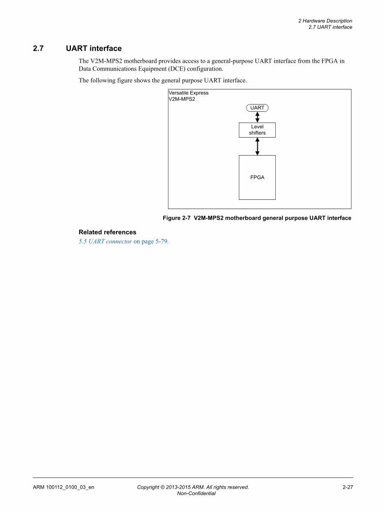
2.7 UART interfaceThe V2M-MPS2 motherboard provides access to a general-purpose UART interface from the FPGA inData Communications Equipment (DCE) configuration.
The following figure shows the general purpose UART interface.
UART
Versatile ExpressV2M-MPS2
FPGA
Levelshifters
Figure 2-7 V2M-MPS2 motherboard general purpose UART interface
Related references5.5 UART connector on page 5-79.
2 Hardware Description2.7 UART interface
ARM 100112_0100_03_en Copyright © 2013-2015 ARM. All rights reserved. 2-27Non-Confidential

2.8 VGA and CLCD interfacesThe V2M-MPS2 motherboard supports VGA and CLCD video output.
Overview of the VGA interface
The VGA interface consists of a VGA controller in the FPGA, a passive resistor network and an outputVGA port. The VGA output has 4 bits per channel color depth.
Overview of the CLCD interface
The CLCD interface consists of an SPI bus connected between the FPGA and a CLCD connector and anLCD touch screen.
The LCD Thin Film Technology (TFT) display panel is fitted to the CLCD connector and has 320x240pixel resolution. The panel includes a 4-wire resistive touch screen and an STEMPE811 touch screencontroller connected to the FPGA over an I2C bus.
The following figure shows the V2M-MPS2 motherboard VGA and CLCD interfaces.
Versatile Express V2M-MPS2
FPGA VGA
CLCD
SPI
VGA
LCD panel
I2C
Touch Screen
controller
Figure 2-8 V2M-MPS2 motherboard VGA and CLCD interfaces.
LCD panel
The LCD panel is configured for SPI graphics and I2C touch-screen.
Related references1.3 Location of components on the V2M-MPS2 motherboard on page 1-14.5.3 CLCD connector on page 5-77.5.7 VGA connector on page 5-81.
2 Hardware Description2.8 VGA and CLCD interfaces
ARM 100112_0100_03_en Copyright © 2013-2015 ARM. All rights reserved. 2-28Non-Confidential
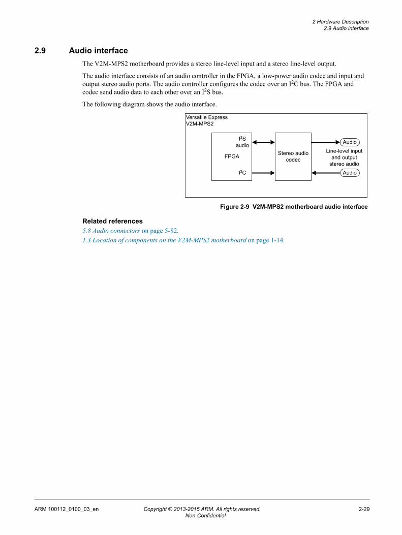
2.9 Audio interfaceThe V2M-MPS2 motherboard provides a stereo line-level input and a stereo line-level output.
The audio interface consists of an audio controller in the FPGA, a low-power audio codec and input andoutput stereo audio ports. The audio controller configures the codec over an I2C bus. The FPGA andcodec send audio data to each other over an I2S bus.
The following diagram shows the audio interface.
Audio
Audio
Versatile ExpressV2M-MPS2
FPGA Stereo audio codec
I2S audio
I2C
Line-level inputand output
stereo audio
Figure 2-9 V2M-MPS2 motherboard audio interface
Related references5.8 Audio connectors on page 5-82.1.3 Location of components on the V2M-MPS2 motherboard on page 1-14.
2 Hardware Description2.9 Audio interface
ARM 100112_0100_03_en Copyright © 2013-2015 ARM. All rights reserved. 2-29Non-Confidential

2.10 Ethernet interfaceThe V2M-MPS2 motherboard provides an Ethernet MAC interface.
Overview of the Ethernet interface.
The Ethernet interface consists of a 16-bit interface on the FPGA, a combined Ethernet MAC and PHYon the board and Ethernet connector for external connection.
Note
The MAC/PHY connects to the same 16-bit interface as the 16MB PSRAM external memory.
The V2M-MPS2 motherboard contains three LEDs that denote Ethernet activity:• LINK LED:
— On denotes Ethernet connection established.— Off denotes Ethernet connection not established.
• DPLX LED:— On denotes connection operating in duplex mode.— Off denotes Ethernet connection operating in simplex mode
• 100Mbs LED:— On denotes Ethernet connection operating at 100Mbs.— Off denotes Ethernet connection operating at 10Mbs.
The following diagram shows the V2M-MPS2 motherboard Ethernet interface.
Ethernet
Versatile ExpressV2M-MPS2
FPGA
MAC/PHY25MHzCLK
16-bit
DPLX
LINK
100Mbs
Ethernet activity LEDs
Figure 2-10 V2M-MPS2 motherboard Ethernet interface
Related concepts2.12 External user memory on page 2-32.
Related references5.9 Ethernet connector on page 5-83.
2 Hardware Description2.10 Ethernet interface
ARM 100112_0100_03_en Copyright © 2013-2015 ARM. All rights reserved. 2-30Non-Confidential

2.11 User switches and user LEDsThe V2M-MPS2 motherboard provides a user interface that consists of user LEDs and user switches thatconnect to the FPGA and MCC. The FPGA image and application software define their meaning.
The board provides the following LEDs and switches:• Two LEDs and two push buttons that connect directly to the FPGA:
— The board labels the LEDs as USERLED0 and USERLED1.— The board labels the push buttons as PB0 and PB1.
• Eight LEDs and an 8-way DIP switch that connect to the MCC.
You can write the values from these LEDs and switches to system registers inside the FPGA using aserial SCC interface.
The following diagram shows the user switches and LEDs that form the FPGA and MCC user interface.
Versatile ExpressV2M-MPS2
PB0
USERLED0
MCC FPGASCC
PB1
USERLED1User DIP switches 1-8
User LEDs 1-8
Figure 2-11 V2M-MPS2 motherboard FPGA and MCC user interface
Related concepts2.13 MCC FPGA serial interface on page 2-35.
Related references1.3 Location of components on the V2M-MPS2 motherboard on page 1-14.4.4.3 SCC_CFG1 Register on page 4-59.4.4.4 SCC_CFG3 Register on page 4-59.
2 Hardware Description2.11 User switches and user LEDs
ARM 100112_0100_03_en Copyright © 2013-2015 ARM. All rights reserved. 2-31Non-Confidential

2.12 External user memoryThe V2M-MPS2 motherboard provides external user ZBT SSRAM and PSRAM memory.
The external user memory connects to the FPGA and consists of the following:• Two 2MB 32-bit fast single-cycle ZBT SSRAM memory:
— These connect to two independent 32-bit memory interfaces on the FPGA.• One 4MB 32-bit fast single-cycle ZBT SSRAM memory:
— This consists of two 2MB 32-bit memories which the board configures as one 64-bit memory.They connect to one 64-bit memory interface on the FPGA.
• Two 16-bit 8MB PSRAM memory:— These supplements the ZBT SSRAM.
Note
The 16MB PSRAM connects to the same 16-bit interface on the FPGA as the Ethernet MAC/PHY.
The MCC can pre-load the external user memory using the images.txt file before releasing reset. Thisenables the V2M-MPS2 motherboard to use the external memory as boot RAM.
The following diagram shows the external ZBT SSRAM user memory interface.
2 Hardware Description2.12 External user memory
ARM 100112_0100_03_en Copyright © 2013-2015 ARM. All rights reserved. 2-32Non-Confidential

Versatile ExpressV2M-MPS2
FPGA
ZBTSSRAM
2MB
ZBTSSRAM
2MB
ZBTSSRAM
2MB
SSRAM1_nCE1SSRAM1_MODE
SSRAM1_ZZSSRAM1_nCENSSRAM1_nOE
SSRAM1_ADVnLDSSRAM1_nWE
SSRAM1_A[18:0]SSRAM1_DQP[7:4]
SSRAM1_DQ[63:0]SSRAM1_ADV_nBW[7:0] SSRAM1_ADV_nBW[7:4]
SSRAM1_ADV_nBW[3:0]
SSRAM1_CLK1
SSRAM1_DQ[63:32]
SSRAM1_DQ[31:0]
SSRAM1_DQP[7:0]
SSRAM1_DQP[3:0]SSRAM1_A[18:0]
SSRAM1_nWESSRAM1_ADVnLD
SSRAM1_nOESSRAM1_nCEN
SSRAM1_ZZSSRAM1_MODESSRAM1_nCE1SSRAM1_CLK0
SSRAM2_CLKSSRAM2_ADV_nBW[3:0]
SSRAM2_DQ[31:0]SSRAM2_DQP[3:0]SSRAM2_A[18:0]
SSRAM2_nWESSRAM2_ADVnLD
SSRAM2_nOESSRAM2_nCEN
SSRAM2_ZZSSRAM2_MODESSRAM2_nCE1
ZBTSSRAM
2MB
SSRAM3_CLKSSRAM3_ADV_nBW[3:0]
SSRAM3_DQ[31:0]SSRAM3_DQP[3:0]SSRAM3_A[18:0]
SSRAM3_nWESSRAM3_ADVnLD
SSRAM3_nOESSRAM3_nCEN
SSRAM3_ZZSSRAM3_MODESSRAM3_nCE1
Figure 2-12 V2M-MPS2 motherboard ZBT SSRAM external user memory interface
The following diagram shows the external PSRAM user memory interface.
2 Hardware Description2.12 External user memory
ARM 100112_0100_03_en Copyright © 2013-2015 ARM. All rights reserved. 2-33Non-Confidential

Versatile ExpressV2M-MPS2
FPGA
PSRAM 8MBSMB_nZZSMB_nOESMB_nWE
SMB_A[21:0]
SMB_nUBSMB_nLB
SMB_DQ[15:0]SMB_PSRAM_nCE[1]
PSRAM 8MB
SMB_PSRAM_nCE[0]
Figure 2-13 V2M-MPS2 motherboard PSRAM external user memory interface
Related concepts2.10 Ethernet interface on page 2-30.
2 Hardware Description2.12 External user memory
ARM 100112_0100_03_en Copyright © 2013-2015 ARM. All rights reserved. 2-34Non-Confidential

2.13 MCC FPGA serial interfaceThis section describes the Serial Configuration Controller (SCC) between the MCC and the FPGA.
This section contains the following subsections:• 2.13.1 Serial Configuration Controller (SCC) on page 2-35.• 2.13.2 SCC READ and WRITE operations on page 2-36.• 2.13.3 SCC READ and WRITE timings on page 2-36.
2.13.1 Serial Configuration Controller (SCC)
The MCC uses a serial communication channel to receive from and transmit information to the FPGA onthe board. You must implement a Serial Configuration Controller (SCC) in the FPGA.
Overview of MCC-SCC interface
The SCC interface operates at 0.5MHz. The serial interface is similar to a memory-mapped peripheralbecause it has an address and data phase.
The nCFGRST output from the MCC loads the default configuration settings into the FPGA.CFGLOAD determines when WRITE DATA is complete, or when the system expects READ DATA tobe ready. The MCC provides the SCC clock. CFGWnR changes depending upon the access type. TheSCC operates a 12-bit address and 32-bit data phase.
The following figure shows the MCC-SCC interface.
Versatile Express V2M-MPS2
FPGA
microSD card(USBMSD)
USB 2.0
MCC
ON/OFF/Soft RESET push button
Hardware RESET push button
SCCregisters
nCFGRSTCFGCLK
CFGDATAINCFGLOADCFGWnR
CFGDATAOUT
Figure 2-14 MCC-FPGA serial interface
FPGA pin assignments to implement an MCC-SCC interfaceIf you implement an SCC interface, you must make the following pin assignments in the FPGA:
assign CFGCLK = CLCD_PDH[13];assign nCFGRST = CLCD_PDH[14];
2 Hardware Description2.13 MCC FPGA serial interface
ARM 100112_0100_03_en Copyright © 2013-2015 ARM. All rights reserved. 2-35Non-Confidential

assign CFGLOAD = CLCD_PDH[15];assign CFGWnR = CLCD_PDH[16];assign CFGDATAIN = CLCD_PHD[17];assign CLCD_PDH[12] = CFGDATAOUT;
Note
See Application Note AN387 ARM® Cortex®-M0 Design Start SMM on V2M-MPS2 for an example scc.vfile that implements these registers.
Note
If the FPGA does not implement an SCC interface, ARM recommends that you tie off theCFGDATAOUT and nRSTREQ signals as follows:• Tie the CFGDATAOUT signal from the FPGA LOW.• Tie the nRSTREQ signal from the FPGA HIGH.
Related concepts2.16 Minimum design settings for motherboard operation on page 2-43.
2.13.2 SCC READ and WRITE operations
During WRITE operations, after clocking in the address and data, CFGLOAD loads the address anddata into the SCC. The MCC clocks the WRITE DATA Most Significant Bit (MSB) first.
During READ operations, after clocking in the address, CFGLOAD loads the read address into the SCC.The SCC clocks the READ DATA Least Significant Bit (LSB) first.
2.13.3 SCC READ and WRITE timings
The following figure shows the timings for the WRITE operation.
CFGCLK
CFGLOAD
nCFGRST
CFGWnR
SCCreset Write address Write data Load address
and data
A11 A10 A0 D31 D30 D0CFGDATAIN D1A9
Figure 2-15 MCC write to SCC
The following figure shows the timings for the READ operation.
2 Hardware Description2.13 MCC FPGA serial interface
ARM 100112_0100_03_en Copyright © 2013-2015 ARM. All rights reserved. 2-36Non-Confidential

A11 A10
CFGCLK
A0
D0 D1 D31
CFGDATAIN
D30
A9
CFGLOAD
nCFGRST
CFGWnR
SCCreset
Write address Read dataLoad address
CFGDATAOUT
Figure 2-16 MCC read from SCC
The following table shows the MCC AC timing requirements.
Table 2-1 MCC AC timing requirements for SCC interface
Variable Time
MCC Clock to output valid time: Tov -500ns
MCC Clockt to output invalid time: Toh 500ns
MCC input setup time: Tis 500ns
MCC input hold time: Tih -500ns
Related concepts2.11 User switches and user LEDs on page 2-31.4.3 Register summary on page 4-57.4.4 SCC register descriptions on page 4-58.
2 Hardware Description2.13 MCC FPGA serial interface
ARM 100112_0100_03_en Copyright © 2013-2015 ARM. All rights reserved. 2-37Non-Confidential

2.14 PowerYou supply power to the V2M-MPS2 motherboard from the mains supply using the on-board connectorand the connector cable that ARM supplies with the board.
ARM supplies an external power supply unit which converts mains power to 12V DC which connects tothe 12V connector on the board. The unit accepts mains power in the range 110V AC to 240V AC.
Alternatively, you can connect an external 12V DC supply, +/- 10%, directly to the 12V connector.
On-board regulators supply power to the V2M-MPS2 motherboard power domains and to the FPGApower domains.
Note
The PWR LED illuminates when the MCC is powered up and active.
Related references5.10 12V power connector on page 5-84.
2 Hardware Description2.14 Power
ARM 100112_0100_03_en Copyright © 2013-2015 ARM. All rights reserved. 2-38Non-Confidential

2.15 Debug and traceThis section describes the debug and trace systems on the V2M-MPS2 motherboard.
This section contains the following subsections:• 2.15.1 Overview of FPGA debug and trace systems on page 2-39.• 2.15.2 F-JTAG on page 2-40.• 2.15.3 P-JTAG on page 2-40.• 2.15.4 4-bit Trace on page 2-41.• 2.15.5 16-bit Trace on page 2-41.• 2.15.6 Serial Wire Debug on page 2-41.• 2.15.7 CMSIS-DAP FPGA debug on page 2-41.
2.15.1 Overview of FPGA debug and trace systems
The V2M-MPS2 motherboard provides several debug and trace interfaces:
• P_JTAG processor debug.• F-JTAG FPGA debug.• 16-bit parallel Trace.• 4-bit parallel Trace.• Serial Wire Debug (SWD).• CMSIS-DAP FPGA debug.
Note
• The availability of system debug depends upon the design that you implement in the FPGA.• The V2M-MPS2 motherboard requires motherboard configuration controller firmware version 2.0.1
or later to support CMSIS-DAP.
The following diagram shows a simplified view of the F-JTAG, P-JTAG, Trace, SWD, and CMSIS-DAPconnections.
Caution
The total current limit for the four P-JTAG connectors, ARM JTAG 20, MICTOR 38, CoreSight™ 20, andCoreSight™ 10 is 50mA.
2 Hardware Description2.15 Debug and trace
ARM 100112_0100_03_en Copyright © 2013-2015 ARM. All rights reserved. 2-39Non-Confidential

Versatile ExpressV2M-MPS2
FPGA
Processordebug
ARM JTAG 20
CoreSight 10
CoreSight 20
MICTOR 38
P-JTAG/SWD
P-JTAG/SWD
P-JTAG/SWD
P-JTAG/SWD
P-JTAG/SWD
P-JTAG/SWD
P-JTAG/SWD
P-JTAG/SWD
P-JTAG/SWD
4-bit Trace 4-bit Trace16-bit Trace
16-bit Trace
JTAG 14
ILAdevice
F-JTAG
MCC
USB 2.0 CMSIS-DAP
CMSIS-DAP
Figure 2-17 Overview of V2M-MPS2 motherboard debug and trace
Note
• The ILA device can be any compatible device, for example, SignalTap II.• The processor debug device can be any compatible debugger, for example SignalTap II.
2.15.2 F-JTAG
The JTAG 14 connector supports F-JTAG, FPGA debug.
The F-JTAG chain connects to the hard TAP controllers in the FPGA. The availability of F-JTAGdepends upon the design which you implement in the FPGA.
Related references1.3 Location of components on the V2M-MPS2 motherboard on page 1-14.5.1.1 JTAG 14 connector on page 5-70.
2.15.3 P-JTAG
The V2M-MPS2 motherboard provides several connectors that support P-JTAG, processor debug.
2 Hardware Description2.15 Debug and trace
ARM 100112_0100_03_en Copyright © 2013-2015 ARM. All rights reserved. 2-40Non-Confidential

• ARM JTAG 20 connector.• CoreSight 10 connector.• CoreSight 20 connector.• MICTOR 38 connector.
The availability of P-JTAG depends upon the design which you implement in the FPGA.
Related references1.3 Location of components on the V2M-MPS2 motherboard on page 1-14.5.1.2 ARM JTAG 20 connector on page 5-71.5.1.3 CoreSight™ 10 connector on page 5-72.5.1.4 CoreSight™ 20 connector on page 5-72.5.1.5 MICTOR 38 connector on page 5-73.
2.15.4 4-bit Trace
The CoreSight 20 connector supports 4-bit Trace on the V2M-MPS2 motherboard.
The availability of 4-bit Trace depends upon the design which you implement in the FPGA.
Related references1.3 Location of components on the V2M-MPS2 motherboard on page 1-14.5.1.4 CoreSight™ 20 connector on page 5-72.
2.15.5 16-bit Trace
The MICTOR 38 connector supports 16-bit Trace on the V2M-MPS2 motherboard.
The availability of 16-bit Trace depends upon the design which you implement in the FPGA.
Related references1.3 Location of components on the V2M-MPS2 motherboard on page 1-14.5.1.5 MICTOR 38 connector on page 5-73.
2.15.6 Serial Wire Debug
The V2M-MPS2 motherboard provides several connectors that support Serial Wire Debug (SWD).
• ARM JTAG 20 connector.• CoreSight 10 connector.• CoreSight 20 connector.• MICTOR 38 connector.
The availability of SWD depends upon the design which you implement in the FPGA.
Related references1.3 Location of components on the V2M-MPS2 motherboard on page 1-14.5.1.2 ARM JTAG 20 connector on page 5-71.5.1.3 CoreSight™ 10 connector on page 5-72.5.1.4 CoreSight™ 20 connector on page 5-72.5.1.5 MICTOR 38 connector on page 5-73.
2.15.7 CMSIS-DAP FPGA debug
The USB 2.0 Full Speed port on the V2M-MPS2 motherboard supports CMSIS-DAP debug.
A workstation running a debugger connects to the CMSIS-DAP port which connects to the MCC. TheMCC implements CMSIS-DAP which runs over JTAG connection to the debug access port in the FPGA.
2 Hardware Description2.15 Debug and trace
ARM 100112_0100_03_en Copyright © 2013-2015 ARM. All rights reserved. 2-41Non-Confidential

The availability of CMSIS-DAP depends on the design that you implement in the FPGA. The V2M-MPS2 motherboard requires motherboard configuration software version 2.0.1 or later to supportCMSIS-DAP.
Related concepts2.5 USB 2.0 Full Speed interface on page 2-25.
2 Hardware Description2.15 Debug and trace
ARM 100112_0100_03_en Copyright © 2013-2015 ARM. All rights reserved. 2-42Non-Confidential

2.16 Minimum design settings for motherboard operationYou must implement a minimum amount of RTL in the FPGA for the V2M-MPS2 motherboard tooperate correctly.
You must tie off the following FPGA signals to generate the minimum RTL in the FPGA for correctmotherboard operation:1. Set the following signals to the inactive HIGH state:
• SMB_PSRAM_nce[1:0].• SMB_ETH_nCS.• SSRAM1_nCE1.• SSRAM2_nCE1• SSRAM3_nCE1
2. Set the SMB chip select to the inactive HIGH state by tying the chip selects SMB_nCS to0b11111111.
3. Set the CFGDATAOUT signal to the inactive LOW state by tying NAND_D[5] to 0b0. Note
This informs the MCC that the V2M-MPS2 motherboard does not implement any of its features.
4. Set the nRSTREQ to the inactive HIGH state by tying NAND_D[7] to 0b1. Note
This prevents nRSTREQ from generating a reset. nRSTREQ is usually a system-wide master softreset signal that is both generated and observed by the JTAG debug box.
Note
ARM recommends that you tie all unused pins to their inactive states.
Related concepts2.13.1 Serial Configuration Controller (SCC) on page 2-35.
2 Hardware Description2.16 Minimum design settings for motherboard operation
ARM 100112_0100_03_en Copyright © 2013-2015 ARM. All rights reserved. 2-43Non-Confidential

Chapter 3Configuration
This chapter describes the powerup and configuration process of the Versatile Express V2M-MPS2motherboard.
It contains the following sections:• 3.1 Overview of the V2M-MPS2 motherboard configuration process on page 3-45.• 3.2 Configuration system on page 3-47.• 3.3 Powerup and configuration process on page 3-48.• 3.4 Reset push buttons on page 3-50.• 3.5 Configuration files on page 3-51.
ARM 100112_0100_03_en Copyright © 2013-2015 ARM. All rights reserved. 3-44Non-Confidential
3.1 Overview of the V2M-MPS2 motherboard configuration processThe MCC, in association with the microSD card, configures the V2M-MPS2 motherboard duringpowerup or reset. Once the configuration process starts after application of power or a press of one of theRESET buttons, the configuration process completes without further intervention from the user.
The microSD card stores the board configuration files, including the board.txt and config.txt files.You can access the microSD card as a Universal Serial Bus Mass Storage Device (USBMSD)
The MCC:
• Reads the FPGA image from the microSD card and loads it into the FPGA.• Sets the board oscillator frequencies using values from the board.txt file.• Configures the FPGA SCC registers using values from the board.txt file• Pre-loads the SRAM with the boot image that the images.txt file defines.
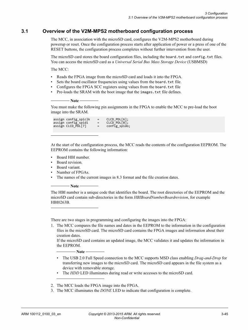
Note
You must make the following pin assignments in the FPGA to enable the MCC to pre-load the bootimage into the SRAM.
assign config_spiclk = CLCD_PDL[6];assign config_spidi = CLCD_PDL[8];assign CLCD_PDL[7] = config_spido;
At the start of the configuration process, the MCC reads the contents of the configuration EEPROM. TheEEPROM contains the following information:
• Board HBI number.• Board revision.• Board variant.• Number of FPGAs.• The names of the current images in 8.3 format and the file creation dates.
Note
The HBI number is a unique code that identifies the board. The root directories of the EEPROM and themicroSD card contain sub-directories in the form HBIBoardNumberBoardrevision, for exampleHBI0263B.
There are two stages in programming and configuring the images into the FPGA:1. The MCC compares the file names and dates in the EEPROM to the information in the configuration
files in the microSD card. The microSD card contains the FPGA images and information about theircreation dates.If the microSD card contains an updated image, the MCC validates it and updates the information inthe EEPROM.
Note
• The USB 2.0 Full Speed connection to the MCC supports MSD class enabling Drag-and-Drop fortransferring new images to the microSD card. The microSD card appears in the file system as adevice with removable storage.
• The HDD LED illuminates during read or write accesses to the microSD card.
2. The MCC loads the FPGA image into the FPGA.3. The MCC illuminates the DONE LED to indicate that configuration is complete.
3 Configuration3.1 Overview of the V2M-MPS2 motherboard configuration process
ARM 100112_0100_03_en Copyright © 2013-2015 ARM. All rights reserved. 3-45Non-Confidential

Related concepts2.5 USB 2.0 Full Speed interface on page 2-25.
3 Configuration3.1 Overview of the V2M-MPS2 motherboard configuration process
ARM 100112_0100_03_en Copyright © 2013-2015 ARM. All rights reserved. 3-46Non-Confidential

3.2 Configuration systemThe V2M-MPS2 motherboard provides hardware infrastructure to enable board configuration duringpowerup or reset.
The following diagram shows the V2M-MPS2 motherboard configuration system.
microSD card(USBMSD)
ConfigurationEEPROM
User DIP switches 1-8
FPGAMCCUSB 2.0 Configuration
Versatile ExpressV2M-MPS2
ON/OFF/Soft RESET push button
Hardware RESET push button
User LEDs 1-8
PB0
USERLED0
PB1
USERLED1
DONE LED
Figure 3-1 V2M-MPS2 motherboard configuration system
Configuration port connected to an external workstation
If you connect an external workstation to the MCC USB 2.0 Full Speed port, you can access theconfiguration memory in the microSD card. You can then edit and copy configuration files and softwareimages to the SD card.
Related concepts2.5 USB 2.0 Full Speed interface on page 2-25.3.5.2 config.txt generic motherboard configuration file on page 3-52.3.5.3 Contents of the V2M-MPS2 motherboard MB directory on page 3-52.3.5.4 Contents of the SOFTWARE directory on page 3-53.3.5.1 Overview of configuration files and microSD card directory structure on page 3-51.
3 Configuration3.2 Configuration system
ARM 100112_0100_03_en Copyright © 2013-2015 ARM. All rights reserved. 3-47Non-Confidential

3.3 Powerup and configuration processThe power push buttons and configuration files control the sequence of events of the V2M-MPS2motherboard powerup and configuration process.
The following figure shows the powerup and configuration process.
Run stateRun boot SRAM image if
present
MCC reads configuration files from microSD card.MCC reads all configuration files and configures the board clocks.
The MCC configures the FPGAs and SCC registers.MCC pre-loads the boot RAM image.
Apply power
You can use the USB 2.0 Full Speed port to edit and update the configuration files in the microSD card.
Standby state
NoON/OFF/Soft Reset button pressed?
No
Hardware RESET button pressed or ON/OFF/Soft Reset button pressed for 2 seconds
MCC reads the EEPROM and does preliminary configuration.
Yes
Resets CB_nPOR and CB_nRST released, processor starts executing code
ON/OFF/Soft Reset button pressed briefly
Assert CB_nPOR and CB_nRST
Hardware RESET or ON/OFF/Soft Reset button pressed?
Figure 3-2 Powerup and configuration sequence
The V2M-MPS2 motherboard powerup and configuration sequence is:1. The board applies power to the system.2. The MCC powers the EEPROM and reads it to determine the HBI identification code for the board.3. The system enters standby mode.4. The system enables the microSD memory card and you can connect a workstation to the MCC USB
2.0 Full Speed port to edit existing configuration files or Drag-and-Drop new configuration files.5. The system stays in standby state until you press the ON/OFF/Soft RESET push button.
3 Configuration3.3 Powerup and configuration process
ARM 100112_0100_03_en Copyright © 2013-2015 ARM. All rights reserved. 3-48Non-Confidential

6. The system loads the board configuration file:• The MCC reads the generic config.txt file.• The MCC searches the microSD card MB directory for the HBI0263x subdirectory that matches
the board HBI code from the board EEPROM.7. The next steps depend on the configuration files:
• If the MCC finds configuration subdirectories that match the HBI code of the V2M-MPS2motherboard, configuration continues and the MCC reads the board.txt file.
• If the MCC does not find the correct configuration files, it records the failure to a log file on themicroSD card. Configuration stops and the system re-enters standby state.
8. The MCC measures the board power supplies.9. The MCC configures the board clocks and FPGA SCC registers.10. If the MCC finds new software images, it loads them into the SRAM through the FPGA.11. The MCC releases the system resets nPOR and nRST, the system enters RUN state.12. Normal operation continues until a new event occurs:
Related concepts3.5.2 config.txt generic motherboard configuration file on page 3-52.3.5.3 Contents of the V2M-MPS2 motherboard MB directory on page 3-52.3.5.4 Contents of the SOFTWARE directory on page 3-53.3.5.1 Overview of configuration files and microSD card directory structure on page 3-51.
3 Configuration3.3 Powerup and configuration process
ARM 100112_0100_03_en Copyright © 2013-2015 ARM. All rights reserved. 3-49Non-Confidential

3.4 Reset push buttonsThe V2M-MPS2 motherboard provides two push buttons which initiate reset and configuration. The tworeset push buttons are the ON/OFF/Soft RESET and the Hardware RESET buttons. This sectiondescribes the use and functions of these push buttons.
This section contains the following subsections:• 3.4.1 ON/OFF Soft RESET button on page 3-50.• 3.4.2 Hardware RESET button on page 3-50.
3.4.1 ON/OFF Soft RESET button
The V2M-MPS2 motherboard provides an ON/OFF/Soft RESET push button that enables you toperform a software reset of the system.
You initiate a software reset of the system by briefly pressing the ON/OFF Soft RESET button during runtime. The MCC performs a software reset of the FPGA and resets the devices on the board It does notperform a full reconfiguration of the FPGA.
The software reset sequence is as follows:1. You briefly press the ON/OFF/Soft RESET button.
Caution
If you press and hold the ON/OFF Soft RESET button for more than two seconds, the system entersthe Standby State in the same way as pressing the Hardware RESET button.
2. The MCC asserts the nRST reset signal. It might also assert nPOR but this depends on the setting ofthe variable ASSERTNPOR in the configuration file config.txt.
3. The MCC releases nPOR if it is active depending on the setting of the variable ASSERTNPOR in theconfiguration file config.txt.
4. The MCC releases nRST.5. The V2M-MPS2 motherboard enters the run state.
Note
The MCC does not read the configuration files or perform a board reconfiguration as a result of asoftware reset.
Related references1.3 Location of components on the V2M-MPS2 motherboard on page 1-14.
3.4.2 Hardware RESET button
The V2M-MPS2 motherboard provides a Hardware RESET push button that enables you to perform ahardware reset of the system.
You can change the operation of the board from ON to Standby by briefly pressing this button. Thisswitches off the power to the board and resets the system to the default values.
If you then press the ON/OFF/Soft RESET push button, the system performs a full configuration andenters the run state.
Related references1.3 Location of components on the V2M-MPS2 motherboard on page 1-14.
3 Configuration3.4 Reset push buttons
ARM 100112_0100_03_en Copyright © 2013-2015 ARM. All rights reserved. 3-50Non-Confidential

3.5 Configuration filesThis section describes the V2M-MPS2 motherboard configuration files in the microSD card whichcontrol the board powerup and configuration process.
This section contains the following subsections:• 3.5.1 Overview of configuration files and microSD card directory structure on page 3-51.• 3.5.2 config.txt generic motherboard configuration file on page 3-52.• 3.5.3 Contents of the V2M-MPS2 motherboard MB directory on page 3-52.• 3.5.4 Contents of the SOFTWARE directory on page 3-53.
3.5.1 Overview of configuration files and microSD card directory structure
Because the V2M-MPS2 motherboard microSD card is non-volatile memory, it is only necessary to loadnew configuration files if you change the system configuration. The V2M-MPS2 motherboard containsdefault configuration files.
If you connect a workstation to the MCC USB 2.0 Full Speed port, the configuration memory device, theSD card, appears as a USB Mass Storage Device (USBMSD) and you can add, edit or delete files.
You can use a standard text editor that produces DOS line endings to read and edit the boardconfiguration files.
The following figure shows a typical example of the directory structure in the microSD card memory.
Caution
Files names and directory names are in 8.3 format:• File names that you generate must be in lower case.• Directory names must be in upper case.• All configuration files must end in DOS line endings (0x0D/0x0A).
config.txtLOG.TXT
V2MMPS2(F:)
MB/HBI0263B/
mbb_v???.ebf
AN???
an???_v?.rbfan???_v?.txt
SOFTWARE/
st_v???.axf
images.txt
board.txt
dm_v???.axf
Figure 3-3 Example USBMSD directory structure
The directory structure and file name format ensure that each image is matched to the correct targetdevice defined in the board configuration EEPROM.• config.txt is the generic configuration file for all motherboards. This file applies to all Versatile
Express motherboards including the V2M-MPS2 motherboard.• The MB directory contains subdirectories for any motherboard variants that might be present in the
system. The subdirectory names match the HBI codes for the specific motherboard variants. The filesin this directory contain clock, register and other settings for the motherboard.
• The SOFTWARE directory contains application files that the MCC can load into the ZBT SSRAM orPSRAM on the board. The images.txt file defines the file that the MCC loads.
3 Configuration3.5 Configuration files
ARM 100112_0100_03_en Copyright © 2013-2015 ARM. All rights reserved. 3-51Non-Confidential

Related concepts2.5 USB 2.0 Full Speed interface on page 2-25.
3.5.2 config.txt generic motherboard configuration file
You can use the V2M-MPS2 motherboard USB 2.0 Full Speed port to update the generic VersatileExpress configuration file config.txt from your workstation to the root directory of the microSD card.
The following example shows a configuration file that you can load into the configuration flash memory. Note
• Colons (:) indicate the end of commands and must be separated by a space character (0x20) from thevalue fields.
• Semicolons (;) indicate comments.
TITLE: Versatile Express V2M-MPS2 configuration file [CONFIGURATION]AUTORUN: FALSE ;Auto Run from power onAUTORUNDELAY: 3 ;Delay in seconds to wait for key press to stop bootupRTC: FALSE ;TRUE = Enable RTC, FALSE = Disable RTC ASSERTNPOR: TRUE ;External resets assert nPORWDTRESET: NONE ;Watchdog reset options NONE/RESETMB/RESETDB USB_REMOTE: TRUE ;Selects remote command via USB MACADDRESS: 0xFFFFFFFFFFFF ;MAC Address
3.5.3 Contents of the V2M-MPS2 motherboard MB directory
The V2M-MPS2 motherboard MB directory contains a configuration HBI subdirectory that matches theHBI code of the board.
The HBI subdirectory contains:• A file of the form mbb_vxxx.ebf. This is an MCC BIOS image.• A board.txt file that defines the MCC bios image.• An application-specific subdirectory that contains the following board configuration files:
— Image files for the FPGA and MCC on the board. These have .rbf extensions.— An images.txt file that defines the .axf files that the MCC loads into external memory during
configuration.— An application note .txt file that defines the number of FPGAs on the board, the number of
oscillators and their frequencies, FPGA and MCC image files and details of the SCC registers.
The following example shows a typical V2M-MPS2 motherboard configuration board.txt file.
BOARD: HBI0263TITLE: Motherboard configuration file [MCCS]MBBIOS mbb_v201.ebf ;MB BIOS IMAGE [APPLICATION NOTE] ;Please select the required processor;APPFILE: AN382\an382_v2.txt ; - Cortex-M0;APPFILE: AN383\an383_v2.txt ; - Cortex-M0+;APPFILE: AN384\an384_v2.txt ; - Cortex-M1APPFILE: AN385\an385_v2.txt ; - Cortex-M3;APPFILE: AN386\an386_v2.txt ; - Cortex-M4;APPFILE: AN387\an387_v2.txt ; - Cortex-M0 Design Start;APPFILE: AN399\an399_v2.txt ; - Cortex-M7;APPFILE: AN400\an400_v2.txt ; - Cortex-M7 with CoreSight
The following example shows a typical V2M-MPS2 motherboard application note .txt file.
BOARD: HBI0263TITLE: Application Note File
3 Configuration3.5 Configuration files
ARM 100112_0100_03_en Copyright © 2013-2015 ARM. All rights reserved. 3-52Non-Confidential

[FPGAS]TOTALFPGAS: 1 ;Total Number of FPGAS (Max : 1)F0FILE: an385_v2.rbf ;FPGA0 FilenameF0MODE: FPGA ;FPGA0 Programming Mode [OSCCLKS]TOTALOSCCLKS: 3OSC0: 50.0 ;OSC0 System clock in MHzOSC1: 24.576 ;OSC1 AACI clock in MHzOSC2: 25.0 ;OSC2 MISC clock in MHz [SCC REGISTERS]TOTALSYSCONS: 1 ;Total Number of SYSCON registers definedSYSCON: 0x000 0x00000001 ;SCC enable ZBT remap
The following example shows a typical V2M-MPS2 motherboard images.txt file.
TITLE: Versatile Express V2M-MPS2 software image configuration file [IMAGES]TOTALIMAGES: 1 ;Number of Images (Max : 32) IMAGE0ADDRESS:0x00000000 ;Please select the required executable programIMAGE0FILE: \SOFTWARE\dm_v111.axf ; - demo;IMAGE0FILE: \SOFTWARE\st_v111.axf ; - selftest
3.5.4 Contents of the SOFTWARE directory
The SOFTWARE directory contains applications that you can load into the ZBT SSRAM or PSRAMmemory.
You can create new applications and load them into the RAM on the V2M-MPS2 motherboard.Application images are typically boot images or demo programs and have a .axf extension.
Typical applications in this directory are:• dm_v102.axf board demonstration software.• st_v103.axf board test software.• user.axf user test software.
3 Configuration3.5 Configuration files
ARM 100112_0100_03_en Copyright © 2013-2015 ARM. All rights reserved. 3-53Non-Confidential

Chapter 4Programmers Model
This chapter describes the programmers model of the Versatile Express V2M-MPS2 motherboard.
It contains the following sections:• 4.1 About this programmers model on page 4-55.• 4.2 Memory map on page 4-56.• 4.3 Register summary on page 4-57.• 4.4 SCC register descriptions on page 4-58.• 4.5 System configuration registers on page 4-65.
ARM 100112_0100_03_en Copyright © 2013-2015 ARM. All rights reserved. 4-54Non-Confidential

4.1 About this programmers modelThe following information applies to the SCC registers and to the system configuration registers orSYS_CFG registers:
• The base address is not fixed, and can be different for any particular system implementation. Theoffset of each register from the base address is fixed.
• Do not attempt to access reserved or unused address locations. Attempting to access these locationscan result in UNPREDICTABLE behavior.
• Unless otherwise stated in the accompanying text:— Do not modify undefined register bits.— Ignore undefined register bits on reads.— All register bits are reset to a logic 0 by a system or powerup reset.— Table 4-1 V2M-MPS2 motherboard SCC register summary on page 4-57 describes register
access type as follows:
RW Read and write.
RO Read only.
WO Write only.
4 Programmers Model4.1 About this programmers model
ARM 100112_0100_03_en Copyright © 2013-2015 ARM. All rights reserved. 4-55Non-Confidential

4.2 Memory mapThe image that you load into the FPGA on the V2M-MPS2 motherboard determines the board memorymap. See the relevant SMM Application Note for an example memory map for the V2M-MPS2motherboard.
4 Programmers Model4.2 Memory map
ARM 100112_0100_03_en Copyright © 2013-2015 ARM. All rights reserved. 4-56Non-Confidential

4.3 Register summaryThis section summarizes the V2M-MPS2 motherboard SCC registers and system configuration registerscharacteristics.
The following table shows the registers in offset order from the base memory address.
Table 4-1 V2M-MPS2 motherboard SCC register summary
Offset Name Type Reset Width Comment
0x000 SCC_CFG0 RW 0x00000000 32 Remaps block RAM to ZBT.
0x004 SCC_CFG1 RW 0x00000000 32 Controls the MCC user LEDs.
0x008 - - - - Reserved. Do not write to or read from this register.
0x00C SCC_CFG3 RO 0x00000000 32 Denotes the state of the MCC user switches.
0x010 SCC_CFG4 RO 0x00000000 32 Denotes the board revision.
0x014 - 0x09C - - - - Reserved. Do not write to or read from these registers
0x0A0 SYS_CFGDATA_RTN RO 0x00000000 32 This is one oUser data return register for reads from boardperipherals.
0x0A4 SYS_CFGDATA_OUT RW 0x00000000 32 User data output register for writes to board peripherals.
0x0A8 SYS_CTRL RW 0x00100000 32 Control register. Controls read and write operations.
0x0AC SYS_CFGSTAT RO 0x00000000 32 Status register. Shows status of read and write operations.
0x0AD - 0x0FC - - - - Reserved. Do not write to or read from these registers.
0x100 SCC_DLL RO 0xFFFC0000 32 DLL Lock Register
0x104 - 0xFF7 - - - - Reserved. Do not write to or read from these registers
0xFF8 SCC_AID RO 0x03100708 32 Contains the FPGA build number, the target board of theFPGA build, and information about the SCC registerimplementation.
0xFFC SCC_ID RO 0x4104XXX1 32 Contains information about the FPGA image.
Related concepts2.13 MCC FPGA serial interface on page 2-35.
Related references4.4.2 SCC_CFG0 Register on page 4-58.4.4.3 SCC_CFG1 Register on page 4-59.4.4.4 SCC_CFG3 Register on page 4-59.4.4.5 SCC_CFG4 Register on page 4-60.4.5.2 SYS_CFGDATA_RTN Register on page 4-66.4.5.3 SYS_CFGDATA_OUT Register on page 4-66.4.5.4 SYS_CFGCTRL Register on page 4-67.4.5.5 SYS_CFGSTAT Register on page 4-68.4.4.6 SCC_DLL Register on page 4-61.4.4.7 SCC_AID Register on page 4-62.4.4.8 SCC_ID Register on page 4-63.
4 Programmers Model4.3 Register summary
ARM 100112_0100_03_en Copyright © 2013-2015 ARM. All rights reserved. 4-57Non-Confidential

4.4 SCC register descriptionsThis section describes the SCC registers on the V2M-MPS2 motherboard FPGA.
This section contains the following subsections:• 4.4.1 Overview of SCC registers on page 4-58.• 4.4.2 SCC_CFG0 Register on page 4-58.• 4.4.3 SCC_CFG1 Register on page 4-59.• 4.4.4 SCC_CFG3 Register on page 4-59.• 4.4.5 SCC_CFG4 Register on page 4-60.• 4.4.6 SCC_DLL Register on page 4-61.• 4.4.7 SCC_AID Register on page 4-62.• 4.4.8 SCC_ID Register on page 4-63.
4.4.1 Overview of SCC registers
The MCC on the V2M-MPS2 motherboard writes to the SCC registers in the FPGA at powerup with thevalues that the configuration board file defines.
During run-time, the MCC polls the LED and switch values to ensure that they match the SCC_CFG1and SCC_CFG2 register values. The MCC updates the LEDs to match the SCC_CFG1 register valuesand updates the SCC_CFG2 register to match the user switches.
The SCC_CFG3 register contains board revision information.
The MCC reads the SYS_DLL, SCC_AID and SCC_ID registers to determine whether the PLLs in theFPGA are locked and to determine the loaded FPGA image.
4.4.2 SCC_CFG0 Register
The SCC_CFG0 Register characteristics are:
PurposeRemaps block RAM to ZBT.
Usage constraintsThere are no usage constraints.
ConfigurationsAvailable in all V2M-MPS2 motherboard configurations.
The following figure shows the bit assignments.
31 0
Reserved
Remap block RAM to ZBT
1
0
Figure 4-1 SCC_CFG0 Register bit assignments
The following table shows the bit assignments.
4 Programmers Model4.4 SCC register descriptions
ARM 100112_0100_03_en Copyright © 2013-2015 ARM. All rights reserved. 4-58Non-Confidential

Table 4-2 SCC_CFG0 Register bit assignments
Bits Name Function
[31:1] - Reserved. Do not write to these bits.
[0] REMAP_BLOCK_RAM_TO_ZBT This bit remaps block RAM to ZBT:• 0b0 Does not remap block RAM to ZBT.• 0b1 Remaps block RAM to ZBT.
Related concepts4.3 Register summary on page 4-57.
4.4.3 SCC_CFG1 Register
The SCC_CFG1 Register characteristics are:
PurposeControls the USER LEDS on the V2M-MPS2 motherboard. The MCC polls this SCC register inthe FPGA and updates the appropriate LEDs.
Usage constraintsThere are no usage constraints.
ConfigurationsAvailable in all V2M-MPS2 motherboard configurations.
The following figure shows the bit assignments.
31 0
Reserved
LED[7:0]
78
0 0 0 0 0 0 0 0
Figure 4-2 SCC_CFG1 Register bit assignments
The following table shows the bit assignments.
Table 4-3 SCC_CFG1 Register bit assignments
Bits Name Function
[31:8] - Reserved. Do not write to these bits.
[7:0] LED[7:0] These bits control the individual USER LEDs:• 0b0 Off• 0b1 On
Related concepts2.11 User switches and user LEDs on page 2-31.4.3 Register summary on page 4-57.
4.4.4 SCC_CFG3 Register
The SCC_CFG3 Register characteristics are:
4 Programmers Model4.4 SCC register descriptions
ARM 100112_0100_03_en Copyright © 2013-2015 ARM. All rights reserved. 4-59Non-Confidential

PurposeDetermines the state of the eight user switches on the V2M-MPS2 motherboard. The MCC pollsthe switches and updates this SCC register in the FPGA.
Usage constraintsThe SCC_CFG3 Register is read-only.
ConfigurationsAvailable in all V2M-MPS2 motherboard configurations.
The following figure shows the bit assignments.
31 0
Reserved
SWITCH[7:0]
78
0 0 0 0 0 0 0 0
Figure 4-3 SCC_CFG3 Register bit assignments
The following table shows the bit assignments.
Table 4-4 SCC_CFG3 Register bit assignments
Bits Name Function
[31:8] - Reserved. Do not write to these bits.
[7:0] SW[7:0] These bits indicate the state of the user switches:• 0b0 Off• 0b1 On
Related concepts2.11 User switches and user LEDs on page 2-31.4.3 Register summary on page 4-57.
4.4.5 SCC_CFG4 Register
The SCC_CFG4 Register characteristics are:
PurposeContains V2M-MPS2 motherboard revision information.
Usage constraintsThe SCC_CFG4 Register is read-only.
ConfigurationsAvailable in all V2M-MPS2 motherboard configurations.
The following figure shows the bit assignments.
31 0
Reserved Board revision
34
Figure 4-4 SCC_CFG4 Register bit assignments
The following table shows the bit assignments.
4 Programmers Model4.4 SCC register descriptions
ARM 100112_0100_03_en Copyright © 2013-2015 ARM. All rights reserved. 4-60Non-Confidential

Table 4-5 SCC_CFG4 Register bit assignments
Bits Name Function
[31:4] - Reserved. Do not write to these bits.
[3:0] Board revision • 0000 = A• 0001 = B• 0010 = C
Related concepts4.3 Register summary on page 4-57.
4.4.6 SCC_DLL Register
The SCC_DLL Register characteristics are:
PurposeDigital Locked Loop (DLL) lock status bits from the FPGA. You read from it to determine thelock status of the DLLs. You can ignore the lock status of some of the DLLs by writing to theDLL_LOCK_MASK bits. The DLLs you ignore depends upon the values of these bits.
Usage constraintsThe SCC_DLL Register is read-only.
ConfigurationsAvailable in all V2M-MPS2 motherboard configurations.
The following figure shows the bit assignments.
31 024 23 16 15 1
DLL_LOCK_MASK
Reserved
DLL_LOCKED[7:0] ALL_UNMASKED_DLLS_LOCKED
1 1 1 1 1 1 1 1 1 1 1 1 1 1 0 0 0
Figure 4-5 SCC_DLL Register bit assignments
The following table shows the bit assignments.
Table 4-6 SCC_DLL Register bit assignments
Bits Name Function
[31:24] DLL_LOCK_MASK[7:0] These bits mask bits[23:16], that is, you ignore the correspondingDLL_LOCKED bits.• 0b0:
— Mask DLL lock status. Corresponding DLL_LOCKED bit, that is thelock status of the corresponding DLL, does not contribute to the value ofbit[0].
• 0b1:— Do not mask DLL lock status. Corresponding DLL_LOCKED bit, that is
the lock status of the corresponding DLL, contributes to the value ofbit[0].
BIT[23:16] DLL_LOCKED[7:0] These bits indicate the lock statuses of the individual DLLs:• 0b0 DLL unlocked.• 0b1 DLL locked.
4 Programmers Model4.4 SCC register descriptions
ARM 100112_0100_03_en Copyright © 2013-2015 ARM. All rights reserved. 4-61Non-Confidential

Table 4-6 SCC_DLL Register bit assignments (continued)
Bits Name Function
[15:1] - Reserved. Do not write to these bits.
[0] ALL_UNMASKED_DLLS_LOCKED This bit indicates whether or not all unmasked DLLs are locked:• 0b0 One or more unmasked DLLs are not locked.• 0b1 All unmasked DLLs are locked.
Related concepts4.3 Register summary on page 4-57.
4.4.7 SCC_AID Register
The SCC_AID Register characteristics are:
PurposeThe SCC_AID Register contains the FPGA build number, the target board of the FPGA build,and information about the SCC register implementation.
Usage constraintsThe SCC_AID Register is read-only.
ConfigurationsAvailable in all V2M-MPS2 motherboard configurations.
The following figure shows the bit assignments.
31 0
Reserved CFGREGNUM
7824 23 11 10 9
SW_ENABLELED_ENABLE
LOCK_ENABLE
FPGA build
Target board
revision
20 19
Figure 4-6 SCC_AID Register bit assignments
The following table shows the bit assignments.
Table 4-7 SCC_AID Register bit assignments
Bits Name Function
[31:24] Build FPGA build number.
[23:20] Target board revision. These bits indicate the target board revision of the FPGA build.• 0000 = A• 0001 = B• 0010 = C
[19:11] - Reserved. Do not write to these bits.
[10] SW_ENABLE This bit indicates whether the system supports the SCC_SW_READ command.
[9] LED_ENABLE This bit indicates whether the system supports the SCC_LED_READ command.
[8] LOCK_ENABLE This bit indicates whether the system supports the SCC_LOCK_READ command.
[7:0] CFGREGNUM These bits indicate the number of user registers you can define. The maximum number is eight.
4 Programmers Model4.4 SCC register descriptions
ARM 100112_0100_03_en Copyright © 2013-2015 ARM. All rights reserved. 4-62Non-Confidential

Related concepts4.3 Register summary on page 4-57.
4.4.8 SCC_ID Register
The SCC_ID Register characteristics are:
PurposeThe MCC reads this register and uses the information to determine information about the designin the FPGA that you can read through the V2M-MPS2 motherboard SYS_CFG interface.
Usage constraintsThe SCC_ID Register is Read-only.
ConfigurationsAvailable in all V2M-MPS2 motherboard configurations.
The following figure shows the bit assignments.
31 0
Variant Revision
24 23
ANImplementer
20 19 16 15
Architecture
Figure 4-7 SCC_ID Register bit assignments
The following table shows the bit assignments.
Table 4-8 SCC_ID Register bit assignments
Bits Name Function
[31:24] Implementer Implementer ID. 0x41 = ARM.
[23:20] Variant Product variant or major revision number: Note
This refers to the core or cluster image in the FPGA and is the x in rxpy
[19:16 IP Architecture Architecture. 0x04 = AHB
[15:4] AN Application Note number.• 382 AN382: V2M-M0 Application Note• 383 AN383: V2M-M0+ Application Note• 384 AN384: V2M-M1 Application Note• 385 AN385: V2M-M3 Application Note• 386 AN386: V2M-M4 Application Note• 387 AN387: V2M-M0 Design Start Application Note• 399 AN399: V2M-M7 Application Note• 400 AN400: V2M-M7 Application Note with CoreSight
[3:0] Revision Product revision or minor revision number. Note
This refers to the core or cluster image in the FPGA and is the y in rxpy
Related concepts4.3 Register summary on page 4-57.
4 Programmers Model4.4 SCC register descriptions
ARM 100112_0100_03_en Copyright © 2013-2015 ARM. All rights reserved. 4-63Non-Confidential

Related concepts2.13 MCC FPGA serial interface on page 2-35.
4 Programmers Model4.4 SCC register descriptions
ARM 100112_0100_03_en Copyright © 2013-2015 ARM. All rights reserved. 4-64Non-Confidential
4.5 System configuration registersThis section describes system configuration registers, that is the SYS_CFG registers.
This section contains the following subsections:• 4.5.1 Overview of system configuration registers on page 4-65.• 4.5.2 SYS_CFGDATA_RTN Register on page 4-66.• 4.5.3 SYS_CFGDATA_OUT Register on page 4-66.• 4.5.4 SYS_CFGCTRL Register on page 4-67.• 4.5.5 SYS_CFGSTAT Register on page 4-68.
4.5.1 Overview of system configuration registers
The system configuration registers enable communication between the MCC and the FPGA.
The configuration, or SYS_CFG, registers are: SYS_CFGDATA_RTN, SYS_CFGDATA_OUT,SYS_CFGCTRL and SYS_CFGSTAT. These registers implement and control write and read operationswhen the application software inside the FPGA writes and reads configuration information to and fromperipherals on the V2M-MPS2 motherboard.
The following block of example pseudo code shows a write operation to write 24MHz to clock generator1.
//Write frequency value to the user data out register. 1: Set SYS_CFGDATAT_OUT = 24000000 //Write to control register. Initiate write process and select clock generator 1 and oscillator function. //This clears Configuration error bit and Configuration complete bit of SYS_CFGSTAT Register. 2: Set SYS_CFGCTRL Start = 1; nREAD_Write_access = 1; Function = 1; Device = 1; //Read status register to determine status of of write operation. 3: Read SYS_CFGSTAT[Configuration error bit, Configuration complete bit] If ( Configuration error bit = 1 ) return TRANSACTION FAIL; If ( Configuration error bit = 0 AND Configuration complete bit = 1) return TRANSACTION OK; If ( Configuration error bit = 0 AND Configuration complete bit = 0) GOTO 1;
The following block of example pseudo code show a read operation to read the frequency of clockgenerator 2.
//Write to control register. Initiate read process and select clock generator 2 and oscillator function. //This clears Configuration error bit and Configuration complete bit of SYS_CFGSTAT Register. 1: Set SYS_CFGCTRL Start = 1; nREAD_Write_access = 0; Function = 1; Device = 2; //Read status register to determine status of of read operation. 2: Read SYS_CFGSTAT[Configuration error bit, Configuration complete bit] If ( Configuration error bit = 1 ) return TRANSACTION FAIL; If ( Configuration error bit = 0 AND Configuration complete bit = 1) return TRANSACTION OK; If ( Configuration error bit = 0 AND Configuration complete bit = 0) GOTO 1;
4 Programmers Model4.5 System configuration registers
ARM 100112_0100_03_en Copyright © 2013-2015 ARM. All rights reserved. 4-65Non-Confidential

4.5.2 SYS_CFGDATA_RTN Register
The SYS_CFGDATA_RTN Register characteristics are:
PurposeThe MCC writes data to the SYS_CFGDATA_RTN Register during a read operation. This datarepresents the value that the addressed V2M-MPS2 motherboard component returns as a resultof the read operation, for example a clock generator frequency.
Usage constraintsThe SYS_CFGDATA_RTN register is read-only to the application software in the FPGA.
ConfigurationsAvailable in all V2M-MPS2 motherboard configurations.
The following figure shows the bit assignments.
31 0
SYS_CFGDATA_RTN[31:0]
000000 0 0 0 0 0 0 00 0 0 0 0 0 0 00 0 0 0 0 0 0 00 0 0
Figure 4-8 SYS_CFGDATA_RTN Register bit assignments
The following table shows the bit assignments.
Table 4-9 SYS_CFGDATA_RTN Register bit assignments
Bits Name Function
[31:0] SYS_CFGDATA_RTN User data register return bits.
Related concepts4.3 Register summary on page 4-57.
4.5.3 SYS_CFGDATA_OUT Register
The SYS_CFGDATA_OUT Register characteristics are:
PurposeThe application software in the FPGA writes data to the SYS_CFGDATA_OUT Register duringa write operation. This data represents a value or function that the write operation sends to theaddressed V2M-MPS2 motherboard component, for example a frequency value to a clockgenerator.
Usage constraintsThere are no usage constraints.
ConfigurationsAvailable in all V2M-MPS2 motherboard configurations.
The following figure shows the bit assignments.
31 0
SYS_CFGDATA_OUT[31:0]
000000 0 0 0 0 0 0 00 0 0 0 0 0 0 00 0 0 0 0 0 0 00 0 0
Figure 4-9 SYS_CFGDATA_OUT Register bit assignments
4 Programmers Model4.5 System configuration registers
ARM 100112_0100_03_en Copyright © 2013-2015 ARM. All rights reserved. 4-66Non-Confidential

The following table shows the bit assignments.
Table 4-10 SYS_CFGDATA_OUT Register bit assignments
Bits Name Function
[31:0] SYS_CFGDATA_OUT User data register output bits.
Related concepts4.3 Register summary on page 4-57.
4.5.4 SYS_CFGCTRL Register
The SYS_CFGCTRL Register characteristics are:
PurposeThe SYS_CFGCTRL Register controls write and read data transfer between the MCC and theSCC interface in the FPGA.
Usage constraintsThere are no usage constraints.
ConfigurationsAvailable in all V2M-MPS2 motherboard configurations.
The following figure shows the bit assignments.
31 026 20 12
Reserved
0 0 0 0 0 0 0
30 29 25 11
StartnRead_Write_access
FunctionReserved
0 0 0 0 0 0 0 0 0 0 0 0 0
Device
0 1
Figure 4-10 SYS_CFGCTRL Register bit assignments
The following table shows the bit assignments.
Table 4-11 SYSCFG_CTRL Register bit assignments
Bits Name Function
[31] Start Writing to this bit generates an interrupt.
[30] nRead_Write_access • 0b0 Read access• 0b1 Write access
[29:26] - Reserved. Do not write to these bits.
[25:20] Function These bits support the following function:• 0b000001 Clock generator
[19:12] - Reserved. Do not write to these bits.
[11:0] Device Selects device to write to or read from:• 0x000 Clock generator 0• 0x001 Clock generator 1• 0x002 Clock generator 2
Related concepts4.3 Register summary on page 4-57.
4 Programmers Model4.5 System configuration registers
ARM 100112_0100_03_en Copyright © 2013-2015 ARM. All rights reserved. 4-67Non-Confidential

4.5.5 SYS_CFGSTAT Register
The SYS_CFGSTAT Register characteristics are:
PurposeThe SYS_CFGSTAT Register contains system configuration status information about read andwrite operations between the application software in the FPGA and the V2M-MPS2motherboard peripherals.
Usage constraintsThe SYS_CFGSTAT Register is read-only.
ConfigurationsAvailable in all V2M-MPS2 motherboard configurations.
The following figure shows the bit assignments.
31 0
00Reserved
Configuration errorConfiguration complete
Figure 4-11 SYS_CFGSTAT Register bit assignments
The following table shows the bit assignments.
Table 4-12 SYS_CFGSTAT Register bit assignments
Bits Name Function
[31:2] - Reserved. Do not write to these bits.
[1] Configuration error A write to SYS_CFGCTRL clears this bit.• 0b0 Configuration successful• 0b1 Configuration failed
[0] Configuration complete A write to SYS_CFGCTRL clears this bit.• 0b0 Configuration not complete• 0b1 Configuration complete
Related concepts4.3 Register summary on page 4-57.
4 Programmers Model4.5 System configuration registers
ARM 100112_0100_03_en Copyright © 2013-2015 ARM. All rights reserved. 4-68Non-Confidential

Chapter 5Signal Descriptions
This chapter describes the signals present at the interface connectors of the Versatile Express V2M-MPS2 motherboard
It contains the following sections:• 5.1 Debug connectors on page 5-70.• 5.2 Expansion connectors on page 5-75.• 5.3 CLCD connector on page 5-77.• 5.4 USB 2.0 connector on page 5-78.• 5.5 UART connector on page 5-79.• 5.6 SPI connector on page 5-80.• 5.7 VGA connector on page 5-81.• 5.8 Audio connectors on page 5-82.• 5.9 Ethernet connector on page 5-83.• 5.10 12V power connector on page 5-84.
ARM 100112_0100_03_en Copyright © 2013-2015 ARM. All rights reserved. 5-69Non-Confidential

5.1 Debug connectorsThis section describes the V2M-MPS2 motherboard connectors that support P-JTAG processor debug, F-JTAG FPGA debug, 16-bit Trace, 4-bit Trace and SWD. This section describes the connectors and liststheir signals.
This section contains the following subsections:• 5.1.1 JTAG 14 connector on page 5-70.• 5.1.2 ARM JTAG 20 connector on page 5-71.• 5.1.3 CoreSight™ 10 connector on page 5-72.• 5.1.4 CoreSight™ 20 connector on page 5-72.• 5.1.5 MICTOR 38 connector on page 5-73.
5.1.1 JTAG 14 connector
The V2M-MPS2 motherboard provides one F-JTAG, ILA, connector that supports FPGA debug. Itenables you to connect an ILA device, such as SignalTap II, to a hard FPGA JTAG chain in the FPGAand debug your design.
The JTAG 14 connector connects to general purpose pins on the FPGA. The availability of F-JTAGdepends upon the design which you implement in the FPGA. The V2M-MPS2 motherboard labels thisconnector as FJTAG.
The following figure shows the JTAG 14 connector.
1 13
2 14
Figure 5-1 JTAG 14 connector
The following table shows the F-JTAG connector pin mapping for each ILA signal on the JTAG 14connector J24.
Table 5-1 JTAG 14 connector, J24, signal list
Pin Signal Pin Signal
1 GND 2 +3V_EXT
3 GND 4 FPGA_TMS
5 GND 6 FPGA_TCK
7 GND 8 FPGA_TDO
9 GND 10 FPGA_TDI
Note
• Pins 4, 8 and 10 have pullup resistors to 3V.• Pin 6 has a pulldown resistor to GND.
Related concepts2.15.2 F-JTAG on page 2-40.
Related references1.3 Location of components on the V2M-MPS2 motherboard on page 1-14.
5 Signal Descriptions5.1 Debug connectors
ARM 100112_0100_03_en Copyright © 2013-2015 ARM. All rights reserved. 5-70Non-Confidential

5.1.2 ARM JTAG 20 connector
The V2M-MPS2 motherboard provides one 3V 20-pin IDC connector that supports P-JTAG processordebug to enable connection of DSTREAM or a compatible third-party debugger. The connector alsosupports SWD.
The ARM JTAG 20 connector connects to general purpose pins on the FPGA. The availability of P-JTAG or SWD depends upon the design which you implement in the FPGA. The V2M-MPS2motherboard labels this connector as PJTAG.
The following figure shows the ARM JTAG 20 connector.
1 19
2 20
Figure 5-2 ARM JTAG 20 connector
The following table shows the pin mapping for each SWD and P-JTAG signal on the ARM JTAG 20connector J4.
Table 5-2 ARM JTAG 20 connector, J4, signal list
Pin Signal Pin Signal
1 3V0_OUT 2 3V0_OUT -optional
3 nTRST 4 GND
5 TDI 6 GND
7 SWDIO/TMS 8 GND
9 SWDCLK/TCK 10 GND
11 GND/RTCK 12 GND
13 SWO/TDO 14 GND
15 nSRST 16 GND
17 NC/DBGRQ 18 GNDDETECT
19 NC/DBACK 20 GND
Note
• The V2M-MPS2 motherboard does not support adaptive clocking. The board ties the RTCK signallow.
• Pins 3, 5, 7, 13, 15 and 18 have pullup resistors to 3V.• Pin 9 has a pulldown resistor to GND.
Related concepts2.15.3 P-JTAG on page 2-40.2.15.6 Serial Wire Debug on page 2-41.
Related references1.3 Location of components on the V2M-MPS2 motherboard on page 1-14.
5 Signal Descriptions5.1 Debug connectors
ARM 100112_0100_03_en Copyright © 2013-2015 ARM. All rights reserved. 5-71Non-Confidential

5.1.3 CoreSight™ 10 connector
The V2M-MPS2 motherboard provides one 3V 10-pin IDC connector. This connector supports P-JTAGprocessor debug to enable connection of DSTREAM or a compatible third-party debugger. Thisconnector also support SWD.
The CoreSight 10 connector connects to general purpose pins on the FPGA. The availability of P-JTAGor SWD depends upon the design which you implement in the FPGA. The V2M-MPS2 motherboardlabels this connector as PJTAG
The following figure shows the CoreSight 10 connector.
1 9
2 10
Figure 5-3 CoreSight 10 connector
The following table shows the pin mapping for each SWD and P-JTAG signal on the CoreSight 10connector J11.
Table 5-3 CoreSight 10 connector, J11, signal list
Pin Signal Pin Signal
1 3V0_OUT 2 SWDIO/TMS
3 GND 4 SWDCLK/TCK
5 GND 6 SWO/TDO
7 KEY 8 NC/TDI
9 GNDDETECT 10 nSRST
Note
• Pins 2, 6, 8 and 10 have pullup resistors to 3V.• Pin 4 on both connectors have pulldown resistors to GND.
Related concepts2.15.3 P-JTAG on page 2-40.2.15.6 Serial Wire Debug on page 2-41.
Related references1.3 Location of components on the V2M-MPS2 motherboard on page 1-14.
5.1.4 CoreSight™ 20 connector
The V2M-MPS2 motherboard provides one 3V 20-pin Cortex debug and ETM connector that supportsP-JTAG processor debug to enable connection of DSTREAM or a compatible third-party debugger. Theconnector also supports SWD and 4-bit Trace.
The CoreSight 20 connector connects to general purpose pins on the FPGA. The availability of P-JTAG,SWD or 4-bit Trace depends upon the design which you implement in the FPGA. The V2M-MPS2motherboard labels this connector as PJTAG
The following figure shows the CoreSight 20 connector.
5 Signal Descriptions5.1 Debug connectors
ARM 100112_0100_03_en Copyright © 2013-2015 ARM. All rights reserved. 5-72Non-Confidential
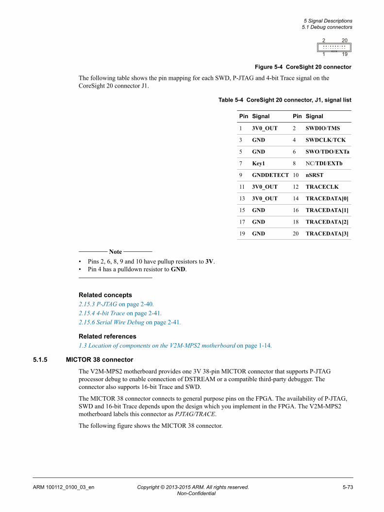
1 19
2 20
Figure 5-4 CoreSight 20 connector
The following table shows the pin mapping for each SWD, P-JTAG and 4-bit Trace signal on theCoreSight 20 connector J1.
Table 5-4 CoreSight 20 connector, J1, signal list
Pin Signal Pin Signal
1 3V0_OUT 2 SWDIO/TMS
3 GND 4 SWDCLK/TCK
5 GND 6 SWO/TDO/EXTa
7 Key1 8 NC/TDI/EXTb
9 GNDDETECT 10 nSRST
11 3V0_OUT 12 TRACECLK
13 3V0_OUT 14 TRACEDATA[0]
15 GND 16 TRACEDATA[1]
17 GND 18 TRACEDATA[2]
19 GND 20 TRACEDATA[3]
Note
• Pins 2, 6, 8, 9 and 10 have pullup resistors to 3V.• Pin 4 has a pulldown resistor to GND.
Related concepts2.15.3 P-JTAG on page 2-40.2.15.4 4-bit Trace on page 2-41.2.15.6 Serial Wire Debug on page 2-41.
Related references1.3 Location of components on the V2M-MPS2 motherboard on page 1-14.
5.1.5 MICTOR 38 connector
The V2M-MPS2 motherboard provides one 3V 38-pin MICTOR connector that supports P-JTAGprocessor debug to enable connection of DSTREAM or a compatible third-party debugger. Theconnector also supports 16-bit Trace and SWD.
The MICTOR 38 connector connects to general purpose pins on the FPGA. The availability of P-JTAG,SWD and 16-bit Trace depends upon the design which you implement in the FPGA. The V2M-MPS2motherboard labels this connector as PJTAG/TRACE.
The following figure shows the MICTOR 38 connector.
5 Signal Descriptions5.1 Debug connectors
ARM 100112_0100_03_en Copyright © 2013-2015 ARM. All rights reserved. 5-73Non-Confidential

2 38
1 37
Figure 5-5 MICTOR 38 connector
The following table shows the pin mapping for each P-JTAG, SWD and 16-bit Trace signal on theMICTOR 38 connector J6.
Table 5-5 MICTOR 38 connector, J6, signal list
Pin Signal Pin Signal
1 NC 2 NC
3 NC 4 NC
5 GND 6 TRACECLK
7 GND 8 GND
9 NC/nSRST 10 GND
11 TDO/SWO 12 3V reference
13 RTCK 14 3V0_OUT
15 TCK/SWCLK 16 TRACEDATA[7]
17 TMS/SWDIO 18 TRACEDATA[6]
19 TDI 20 TRACEDATA[5]
21 nTRST 22 TRACEDATA[4]
23 TRACEDAT[15] 24 TRACEDATA[3]
25 TRACEDAT[14] 26 TRACEDAT[2]
27 TRACEDATA[13] 28 TRACEDATA[1]
29 TRACEDATA[12] 30 GND
31 TRACEDATA[11] 32 GNDDETECT
33 TRACEDATA[10] 34 3V reference
35 TRACEDATA[9] 36 TRACECTL
37 TRACEDATA[8] 38 TRACEDATA[0]
Note
• Pins 9, 11, 17, 19 and 21 have pullup resistors to 3V.• Pin 15 has a pulldown resistor to GND.
Related concepts2.15.3 P-JTAG on page 2-40.2.15.5 16-bit Trace on page 2-41.2.15.6 Serial Wire Debug on page 2-41.
Related references1.3 Location of components on the V2M-MPS2 motherboard on page 1-14.
5 Signal Descriptions5.1 Debug connectors
ARM 100112_0100_03_en Copyright © 2013-2015 ARM. All rights reserved. 5-74Non-Confidential

5.2 Expansion connectorsThe V2M-MPS2 motherboard provides two IDC header connectors that support user expansion.
The following figure shows the IDC expansion connector.
1 332 34
Figure 5-6 IDC expansion connector
The following two tables show the pin mappings for the IDC expansion connectors EXP1, componentnumber J7, and EXP2, component number J8, which support general purpose IO expansion.
Table 5-6 Expansion connector EXP1, J7, signal list
Pin Signal Pin Signal
1 EXP0 2 EXP14
3 EXP1 4 EXP15
5 EXP2 6 EXP16
7 EXP3 8 EXP17
9 EXP4 SI Clock output 10 EXP18
11 GND 12 GND
13 EXP5 SI Clock output 14 EXP19 Clock output
15 EXP6 16 EXP20
17 EXP7 18 EXP21
19 EXP8 20 EXP22
21 EXP9 22 EXP23
23 EXP10 24 GND
25 EXP11 SI Clock output 26 3V
27 3V 28 GND
29 GND 30 3V
31 EXP12 32 EXP24
33 EXP13 34 EXP25
Pins 9, 13, 14, and 25 of connector EXP1 have source series terminating resistors. These resistors help tomaintain the integrity of high slew-rate signals. ARM recommends these pins for use as clock outputs orsensitive data outputs in preference to other pins.
Table 5-7 Expansion connector EXP2, J8, signal list
Pin Signal Pin Signal
1 EXP26 2 EXP40
3 EXP27 4 EXP41
5 EXP28 6 EXP42
7 EXP29 8 EXP43
5 Signal Descriptions5.2 Expansion connectors
ARM 100112_0100_03_en Copyright © 2013-2015 ARM. All rights reserved. 5-75Non-Confidential

Table 5-7 Expansion connector EXP2, J8, signal list (continued)
Pin Signal Pin Signal
9 EXP30 Clock output 10 EXP44 Clock output
11 GND 12 GND
13 EXP31 Clock output 14 EXP45
15 EXP32 16 EXP46
17 EXP33 18 EXP47
19 EXP34 20 EXP48
21 EXP35 22 EXP49 Clock input
23 EXP36 24 GND
25 EXP37 26 3V
27 3V 28 GND
29 GND 30 3V
31 EXP38 32 EXP50 Clock output
33 EXP39 34 EXP51
Note
• Pins 9, 10, 13, 22 and 32 of connector EXP2 have source series termination resistors. These resistorshelp to maintain the integrity of high-slew rate signals:— ARM recommends pins 9, 10, 13 and 32 for use as clock outputs or sensitive data outputs in
preference to other pins.— ARM recommends pin 22 of connector EXP2 for use as a clock input in preference to other pins.
Related concepts2.4 User expansion port on page 2-24.
Related references1.3 Location of components on the V2M-MPS2 motherboard on page 1-14.
5 Signal Descriptions5.2 Expansion connectors
ARM 100112_0100_03_en Copyright © 2013-2015 ARM. All rights reserved. 5-76Non-Confidential

5.3 CLCD connectorThe V2M-MPS2 motherboard provides a female IDC connector that supports CLCD.
The following figure shows the CLCD connector.
1
2
33
34
Figure 5-7 CLCD connector
Note
A mark on the V2M-MPS2 motherboard indicates pin 1.
The following table shows the pin mapping for the CLCD connector J9.
Table 5-8 CLCD connector, J9, signal list
Pin Signal Pin Signal
1 CLCD_T_SCL 2 CLCD_T_SDA
3 CLCD_CS 4 CLCD_RS
5 CLCD_WR_SCL 6 CLCD_RD
7 CLCD_RESET 8 CLCD_PD1
9 CLCD_PD2 10 CLCD_PD3
11 CLCD_PD4 12 CLCD_PD5
13 NC 14 NC
15 NC 16 NC
17 NC 18 NC
19 NC 20 NC
21 NC 22 NC
23 NC 24 GND
25 CLCD_BL_CTRL 26 3V
27 3V 28 GND
29 GND 30 3V
31 CLCD_SDO 32 CLCD_SDI
33 CLCD_T_CS 34 CLCD_T_SCK
Note
Pins 1, 2, 5, 31, and 32 have 10k pullup resistors to 3V.
Related concepts2.8 VGA and CLCD interfaces on page 2-28.
Related references1.3 Location of components on the V2M-MPS2 motherboard on page 1-14.
5 Signal Descriptions5.3 CLCD connector
ARM 100112_0100_03_en Copyright © 2013-2015 ARM. All rights reserved. 5-77Non-Confidential

5.4 USB 2.0 connectorThe V2M-MPS2 motherboard provides one USB 2.0 mini-B connector that provides a USB 2.0 FullSpeed port. This port supports configuration file editing in the microSD, virtual UART access to theFPGA, and CMSIS-DAP FPGA debug.
The following figure shows the USB 2.0 mini-B connector.
Pin 1Pin 5
Figure 5-8 USB 2.0 mini-B connector
The following table shows the pin mapping for the USB 2.0 mini-B connector J14.
Table 5-9 USB 2.0 mini-B connector, J14, signal list
Pin Signal Pin Signal
1 MSD5V 2 MSD_DMRAW
3 MSD_DPRAW 4 MSD_ID
5 GND 6 GND_EARTH
Note
• The GND_EARTH connection is the casing of the mini-B connector.
Related concepts2.5 USB 2.0 Full Speed interface on page 2-25.
Related references1.3 Location of components on the V2M-MPS2 motherboard on page 1-14.
5 Signal Descriptions5.4 USB 2.0 connector
ARM 100112_0100_03_en Copyright © 2013-2015 ARM. All rights reserved. 5-78Non-Confidential

5.5 UART connectorThe V2M-MPS2 motherboard provides one general-purpose female UART connector that supportsaccess to the FPGA.
The general-purpose UART connector connects through a level-shifter to the FPGA. The meaning of theUART signals depends upon the design which you implement in the FPGA.
The following figure shows the general-purpose UART connector.1 2
6 7 8 9
3 4 5
Figure 5-9 General-purpose female UART connector
The following table shows the pin mapping for the general-purpose UART connector J20.
Table 5-10 general-purpose UART connector, J20, signal list
Pin Signal
1 NC
2 SER_RX
3 SER_TX
4 NC
5 SER_GND
6 NC
7 SER_RTS
8 SER_CTS
9 NC
Note
SER_RTS loops back to connect to SER_CTS.
Related concepts2.7 UART interface on page 2-27.
Related references1.3 Location of components on the V2M-MPS2 motherboard on page 1-14.
5 Signal Descriptions5.5 UART connector
ARM 100112_0100_03_en Copyright © 2013-2015 ARM. All rights reserved. 5-79Non-Confidential

5.6 SPI connectorThe V2M-MPS2 motherboard provides one general purpose SPI connector that supports access to theFPGA.
The general purpose SPI connector connects to the FPGA. The meaning of the SPI signals depends uponthe design which you implement in the FPGA.
The following figure shows the general purpose SPI connector.
1
2
5
6
Figure 5-10 general purpose SPI connector
The following table shows the pin mapping for the general purpose SPI connector J21.
Table 5-11 General purpose SPI connector, J21, signal list
Pin Signal
1 GND
2 SPI_SCK
3 SPI_MISO
4 SPI_nSS
5 3V_EXT
6 SPI_MOSI
Related concepts2.6 SPI interface on page 2-26.
Related references1.3 Location of components on the V2M-MPS2 motherboard on page 1-14.
5 Signal Descriptions5.6 SPI connector
ARM 100112_0100_03_en Copyright © 2013-2015 ARM. All rights reserved. 5-80Non-Confidential

5.7 VGA connectorThe V2M-MPS2 motherboard provides one VGA connector that supports VGA and CLCD output.
The VGA connector connects to the VGA controller which connects to general purpose pins on theFPGA. The availability of VGA or CLCD depends upon the design which you implement in the FPGA.
The following figure shows the VGA connector.
Pin 1Pin 5
Pin 11Pin 15
Pin 6Pin 10
Figure 5-11 VGA connector
The following table shows the pin mapping for the VGA connector J10.
Table 5-12 VGA connector, J10, signal list
Pin Signal Pin Signal
1 RED 2 GREEN
3 BLUE 4 NC
5 GND 6 GND
7 GND 8 GND
9 NC 10 GND
11 NC 12 NC
13 HSYNC 14 VSYNC
15 NC
Related concepts2.8 VGA and CLCD interfaces on page 2-28.
Related references1.3 Location of components on the V2M-MPS2 motherboard on page 1-14.
5 Signal Descriptions5.7 VGA connector
ARM 100112_0100_03_en Copyright © 2013-2015 ARM. All rights reserved. 5-81Non-Confidential

5.8 Audio connectorsThe V2M-MPS2 motherboard provides two 3.5mm stereo jack connectors that connect to a low powerstereo audio codec. The two connectors provide an independent line-level stereo input and anindependent line-level stereo output.
The audio codec connects to general purpose pins on the FPGA. The availability of an audio controllerdepends upon the design which you implement in the FPGA.
The following figure shows the audio connector. Audio In is component number J32 and Audio Out iscomponent number J33 on the board.
Figure 5-12 Audio connector
Related concepts2.9 Audio interface on page 2-29.
Related references1.3 Location of components on the V2M-MPS2 motherboard on page 1-14.
5 Signal Descriptions5.8 Audio connectors
ARM 100112_0100_03_en Copyright © 2013-2015 ARM. All rights reserved. 5-82Non-Confidential

5.9 Ethernet connectorThe V2M-MPS2 motherboard provides one 100Mb/s Ethernet connector.
The Ethernet connector connects to the MAC/PHY on the V2M-MPS2 motherboard. The MAC/PHYconnects to general purpose pins on the FPGA. The availability of the Ethernet function depends uponthe design which you implement in the FPGA.
The following figure shows the Ethernet connector J31.
Figure 5-13 Ethernet connector
Related concepts2.10 Ethernet interface on page 2-30.
Related references1.3 Location of components on the V2M-MPS2 motherboard on page 1-14.
5 Signal Descriptions5.9 Ethernet connector
ARM 100112_0100_03_en Copyright © 2013-2015 ARM. All rights reserved. 5-83Non-Confidential

5.10 12V power connectorThe V2M-MPS2 motherboard provides a Thru-hole DC power jack for connecting external power to theboard.
Connect the external mains power supply unit, which ARM supplies, to the power jack.
Alternativley, you can connect an external 12V, +/- 10%, power supply to the power jack to supplypower to the board.
Note
The center pin is the positive side of the power supply.
Related concepts2.14 Power on page 2-38.
Related references1.3 Location of components on the V2M-MPS2 motherboard on page 1-14.
5 Signal Descriptions5.10 12V power connector
ARM 100112_0100_03_en Copyright © 2013-2015 ARM. All rights reserved. 5-84Non-Confidential

Appendix A.1Specifications
This chapter contains the electrical specification of the Versatile Express V2M-MPS2 motherboard andFPGA.
It contains the following sections:• A.1.1 Electrical specification on page Appx-A-86.
ARM 100112_0100_03_en Copyright © 2013-2015 ARM. All rights reserved. Appx-A.1-85Non-Confidential

A.1.1 Electrical specificationThis section provides information on the current characteristics of the Versatile Express V2M-MPS2motherboard. It also supplies information to help you implement your design in the FPGA withoutexceeding the power and current ratings of the board and the temperature rating of the FPGA.
This section contains the following subsections:• FPGA current requirements on page Appx-A-86.
FPGA current requirements
See http://altera.com for software to help you calculate the current requirements for your particularapplication.
The following table shows the power available for each power domain, or group of power domains, ofthe FPGA.
Table A-1 Available FPGA current
FPGA power domain Board powersupply
Voltage Maximum availablecurrent from boardpower supply
Comment
VCCO_3V0
VCCPD_3V0
VCCPGM
VREF_3V
3V 3V 50mA -
VBATT VBAT 3V - -
VCC 1V1 1V1 2.5A -
VCCAUX
VCCO_2V5
VCCPD_2V5
VREF_2V5
VCCA_FPLL
2V5 2V5 1.5A An analog filter on the V2M-MPS2motherboard smooths the supply to theVCCA_FPLL domain.
Caution
• Some FPGA designs might exceed the current and temperature rating of the board. Therefore youmust estimate the power requirements of such designs, using tools such as Quartus II beforeimplementation.
• The FPGA package has a thermal resistance of 13.7° per Watt. The recommended maximum FPGAjunction temperature is 85°C.
A.1 SpecificationsA.1.1 Electrical specification
ARM 100112_0100_03_en Copyright © 2013-2015 ARM. All rights reserved. Appx-A.1-86Non-Confidential

Appendix B.2Revisions
This chapter describes the technical changes between released issues of this book.
It contains the following sections:• B.2.1 Revisions on page Appx-B-88.
ARM 100112_0100_03_en Copyright © 2013-2015 ARM. All rights reserved. Appx-B.2-87Non-Confidential

B.2.1 RevisionsThis appendix describes the technical changes between released issues of this book.
Table B-1 Issue A
Change Location Affects
No changes, first release - -
Table B-2 Difference between issue A and issue B
Change Location Affects
Added application notes AN399 and AN400. Additional reading on page 8 All revisions of board.
Table B-3 Differences between issue B and issue C
Change Location Affects
Added CMSIS-DAP FPGA debug. Throughout document All revisions of board.
Corrected SCC register descriptions. 4.3 Register summary on page 4-57
4.4 SCC register descriptions on page 4-58
All revisions of board.
Updated example configuration files. 3.5.3 Contents of the V2M-MPS2 motherboard MB directoryon page 3-52
All revisions of board.
Table B-4 Difference between issue DDI0525C and issue 100112-0100-03
Change Location Affects
Document number changed from ARM DDI0525 to 100112. Throughout document All revisions of board.
B.2 RevisionsB.2.1 Revisions
ARM 100112_0100_03_en Copyright © 2013-2015 ARM. All rights reserved. Appx-B.2-88Non-Confidential