architectures for emerging communication processing systems
TRANSCRIPT
Architectures for Emerging Communication
Processing SystemsInvited Talk - Oakland EastBay Chapter, IEEE
Communications Society
September 21, 2006
Dilip Krishnaswamy ([email protected]), Ph.D.
Platform Architect, Intel Mobility Group

2
Overview
• Communication Processing Systems definition (for the talk)
• SoC platform architectures– Platform architecture optimization design vectors– 3D SoC platform architectures
• Platform architecture differentiation features– Security, manageability, virtualization
• Multi-protocol multi-channel multi-radio capabilities
• OverMesh: Network Centric Computing– Cross-layer Cross-overlay system architectures– Proactive Adaptive processing over heterogeneous networks

3
Communication Processing Systems considered here
• System architecture for a node with integrated computing and communications processing
• System architecture with multiple nodes involved in distributed computation and communication over heterogeneous networks

4
SoC Platform Architectures
• Optimize vectors such as performance, power, area, latencies, cost, energy/battery life, system efficiency
• Develop a high-performance low power embedded SoC arch
• Support multiple wireless protocols
• Take advantage of small protocol code size requirements
• Low latencies/high perf with integrated on-chip memory
• Consider options to keep memory closer to processors
• Choose memory size sufficient for comm and apps
• Dynamic power management with reduced leakage
• Energy-efficient performance architecture for comm and apps sub-systems
5
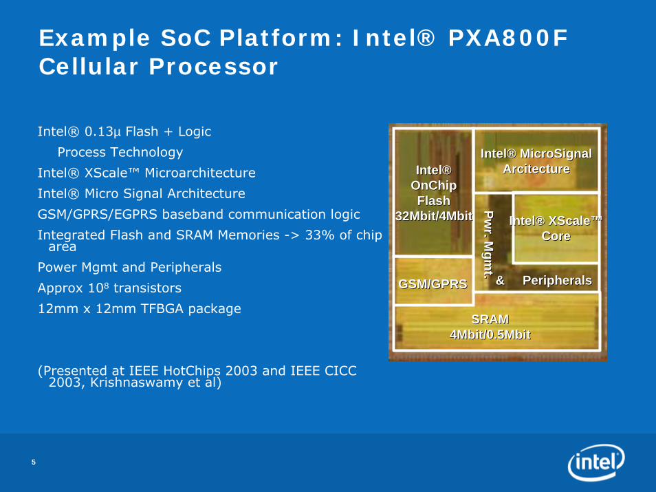
Intel® 0.13µ Flash + Logic
Process Technology
Intel® XScale™ Microarchitecture
Intel® Micro Signal Architecture
GSM/GPRS/EGPRS baseband communication logic
Integrated Flash and SRAM Memories -> 33% of chip area
Power Mgmt and Peripherals
Approx 108 transistors
12mm x 12mm TFBGA package
(Presented at IEEE HotChips 2003 and IEEE CICC 2003, Krishnaswamy et al)
IntelIntel®®OnChipOnChipFlashFlash
32Mbit/4Mbit32Mbit/4Mbit
IntelIntel®® MicroSignalMicroSignalArcitectureArcitecture
IntelIntel®® XScaleXScale™™CoreCore
& Peripherals& Peripherals
SRAMSRAM4Mbit/0.5Mbit4Mbit/0.5Mbit
Pwr. M
gmt.
Pwr. M
gmt.
GSM/GPRSGSM/GPRS
Example SoC Platform: Intel® PXA800F Cellular Processor

6
Chip Modules

7
IntelIntel®® PXA800F/PXA800EF:PXA800F/PXA800EF:2.5G GSM/ GPRS Class 12/EGPRS Class 32.5G GSM/ GPRS Class 12/EGPRS Class 3
Complete Integrated baseband solutionIntel® XScale™ Microarchitecture
ARM* V5TE compliantIntel® Micro Signal Architecture
Modified Harvard Architecture36 Mb integrated Intel® OnChip Flash memory4.5 Mb integrated SRAM memory
Total solutionGSM/GPRSClass 12/EGPRS Class3L1-L3 Comm protocol software RTOS Java-based platformDesigned for use with industry-proven mixed signal/RF solutions Optimized PowerMgmt IC (Dialog)Handset reference design (Elektrobit)
Intel® Micro Signal
Architecture
GSM/GPRS Logic
Intel® PXA800FCellular Processor
Intel® OnChipFlash
32Mbit
SRAM4Mbit
Peripherals
Intel®XScale™ Core
RXTX
AnalogMixed Signal
RFTransceiver
Dialog PowerManagement
Keypad
369
258
147
#0*
Display SIM
Intel® OnChipFlash4Mbit
SRAM512Kbit
*Other names and brands are the property of their respective owners

8
IntelIntel®® MSA CoreMSA Core
External Memory Peripherals
Integrated Flash/SRAM
Integrated Flash/SRAMIntelIntel®® XScale core
DMA
• Wide independent buses from each core to integrated memories Internal memory buses provide direct accesses to memories; can be are wider and faster
• Traditionally phone designs access memories from shared buses with arbitration penalties across narrow higher latency external memory interfaces which impacts performance
• Separate buses to access peripherals/ext mem
Parallelism/Concurrency

9
0%
20%
40%
60%
80%
100%
120%
Syst
em M
emor
y A
cces
s La
tenc
ies
Lower Latencies Through Integration!
External SDRAM
Integrated FlashIntegrated SRAM
• System-level latencies to integrated memories greatly improved due to direct access and optimized design
• Critical-word first latencies in the Intel® XScale™ core sub-system as a %age of external memory access time
Reduced System Level Latencies

10
0%
20%
40%
60%
80%
100%
120%
Peak
Act
ive
Syst
em P
ower
Lower Active System Power!
External SDRAM
Integrated Flash/SRAM
• Total Active System level power is reduced when not using external memory
• Power shown relative to system power when using external memory
Active power usage optimization

11
• Reduced Power * Reduced Latencies (Time) – Reduced Energy
• Lower energy needed for task completion
• System moves to a lower power mode earlier
• Power = VI (Leakage) & CV2F (activity) components
• Reduction in energy usage increases battery life
Energy Minimization

12
Mode
Cores Peripherals PLLs I/O Ring
VCXO
13MHz
Osc
RTC
Active On On On Active On On
On
Standby
Cores Inactive
Clocks Inactive
Reduced Leakage
States Retained
Inactive (except detection logic running with slow clock 32KHz)
OffInactive (sensing
asynchronous inputs)
Off On
Power OffPowered Off
(Real time clock active)Off Off Off Off On
IdleCores Inactive
Clocks Disabled
Inactive
(SW disable
+Clocks disable)
On Active On
Power Modes
13
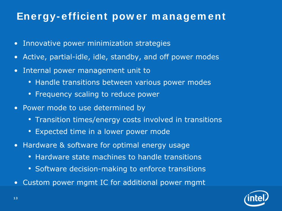
• Innovative power minimization strategies
• Active, partial-idle, idle, standby, and off power modes
• Internal power management unit to
• Handle transitions between various power modes
• Frequency scaling to reduce power
• Power mode to use determined by
• Transition times/energy costs involved in transitions
• Expected time in a lower power mode
• Hardware & software for optimal energy usage
• Hardware state machines to handle transitions
• Software decision-making to enforce transitions
• Custom power mgmt IC for additional power mgmt
Energy-efficient power management

14
• I/O digital buffers from the processor->memory interface exhibit a frequency spectrum determined by their edge-rates
• Faster edge-rates have broader frequency spectrum
• Spectrum can have RF components that interfere with the RF Rx channels
• Wireless data-centric phones suffer much worse due to extreme data transfer between a chip and external memories
• No I/O buffers in access path to integrated memories
• RF Edge Rate Noise Effects Reduced
RF Edge-Rate Noise

15
Benefits of memory integration
• Lower cache miss penalties
• Direct execution from integrated memories
• Higher System-level performance
• Lower power (less power wasted on the pins)
• Wider independent paths from memory to cache
• Outstanding response times during peak loading and task switching
• Greater Peak MIPS availability
• Reduces RF Edge Rate Noise Effects
• Reprogrammable Flash memory for communication and application sub-systems

16
Apps Sub-system
Peripherals/SRAM External Memory (Apps Code/Data)
(Comms Code/Data)
Integrated SRAM/ROM
Integrated SRAM/ROMComms Sub-system
Multimedia/Graphics
Worst case performance optimization needs to consider all possible data flows
Performance Optimization

17
Key Architectural Considerations
• Parallelism
• Integrated memory size optimized for area/performance
• Reduced System-level latencies
• Higher System-level Performance
• Reduced System-level power
• Lower Energy
• Reduced RF Edge Rate Noise Effects
• Lower Cost for overall platform
• Reduced Area for the platform

18
3D Architectures – the future
• Die-to-die interfaces, Through-Silicon-Vias (not merely conventional stacking)
• 3D extension of on-chip integration
• Reduced area footprint and more memory and logic possible
• Reduced distances, Parallelism, Energy/Performance Optimization
• See Ieong et al, IEEE CICC 2003, on 3D ICs, Tsui et al, IEEE Packaging Technology Conference 2003, on Thru-Silicon-Vias.
Die1
Die 3
Die 2

19
Secure Manageable Virtualized Platform Architectures
See IEEE ComSoc Magazine, Sep 2006, “Secure Manageable Mobile Platforms”, Krishnaswamy, Hasbun, & Brizek

20
Useful Security Features
TransitiveRoot-of-Trust
Key Hierarchies
Key and Data-flowManagement

21
Wireless communications Multiprotocol, Multichannel, Multiradio
• Multiple protocols
UWB for short range
WLAN for medium range
WiMAX/LTE/cellular for longer range
• Use multiple radios or reconfigurable radios for support for multiple protocols
• Use multiple channels with multiple radios for simultaneous communication

22
802.16
Bandwidth
2.5G/3G
WWANWWAN
100m
WLANWLANWPANWPAN
802.11a/g
802.11b
10m<1m
10 Mbps
100 Mbps
1 Gbps
1 Mbps
802.11n
Bluetooth*, Zigbee*Low Speed WPANs
WiMedia*/WiMedia*/UWBUWB
Desktop Room Building Community
10 Gbps
Multiprotocol Wireless communications

23
Narrowband BW ~ 10 kHz
801.11BW ~ 20 MHz
UWB 7.5 GHz
Frequency
Part 15 Limit
Pow
erWhy is it compelling?
Offers rich-content video streaming at low power
Complements and extends WiFi just as USB does for Ethernet
Can support Wireless USB, IP, 1394, and Bluetooth protocols
Can support up to 48 devices per host
What is UWB?
High-speed point-point wireless
Unprecedented 7.5 GHz span allocated
480Mbps @ 3m, 100Mbps @ 10m, with multi-Gbps future
UWB – High-level view

24
• 75ns exponential fading matlab modeling for 802.11a/g PHY
• T(x)= A / (1 + e–λ(x– δ)) (Sigmoid modeling, Krishnaswamy, IEEE VTS 2002, 3G Wireless 2002)
54 Mbps = [(48 channels * 6 bits/symbol ) / (4us/symbol) ] * (3/4)
802.11a/g WLAN protocol performance

25
• Node optimizations at a single node may not be sufficient
• MIMO technology can deliver higher data rates
• Matlab modeling of a 2x3 MIMO channel Tx – SFC (Spatial Freq Comb), Rx – MMSE, Fading-75ns exponential
802.11n WLAN protocol performance

26
• Current OFDM based systems
• 64pt FFT, 20 MHz channels (48 channels used for data)
• 2x3 MIMO systems 108 Mbps
• Packet aggregation
• 40MHz channels -> 216Mbps
• 4x4 or 4x5 MIMO systems -> 432 Mbps
• 128pt FFT with 40MHz channels -> use more than 96 (48 *2) channels 500Mbps
• Use QC-LDPC codes to approach Shannon limit 72 * 8
->>> approaching 576Mbps
Emerging 802.11n standard

27
WiMAX performance projections

28
Future Wireless NetworksVision - decentralized, scalable, and dynamically configured wireless network architectures
Scalability Opportunities:
• MultiTier Heterogeneous Mesh Networks, NodeInTheNetwork
• ClientAP, P2P Comm
• Multi-channel, Multi-radio, Multi-hop
• Reconfigurable multi-radios
• Distributed/Mobile/WiMAX portals
Challenges :
• Network scalability, Traffic Engineering
• End-to-End QoS (Bandwidth/latency)
• Load balancing with reduced congestion at portals (wireless/wired interfaces)
• Flexibility, Adaptivity, Fault tolerance
Internet
PortalPortal/controller
AP
AP AP Y
WiMaxRouter
AP
load balancing
AP X
Client AP Client AP
AB
Tier 1
Tier 2
Tier 3
29
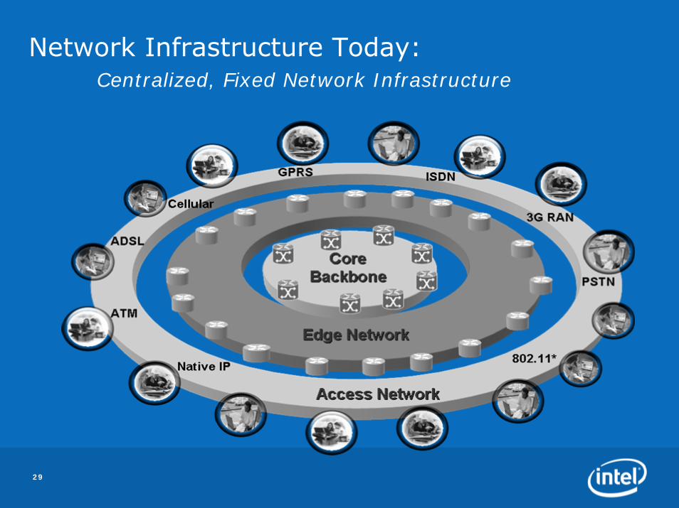
Network Infrastructure Today:Centralized, Fixed Network Infrastructure
30
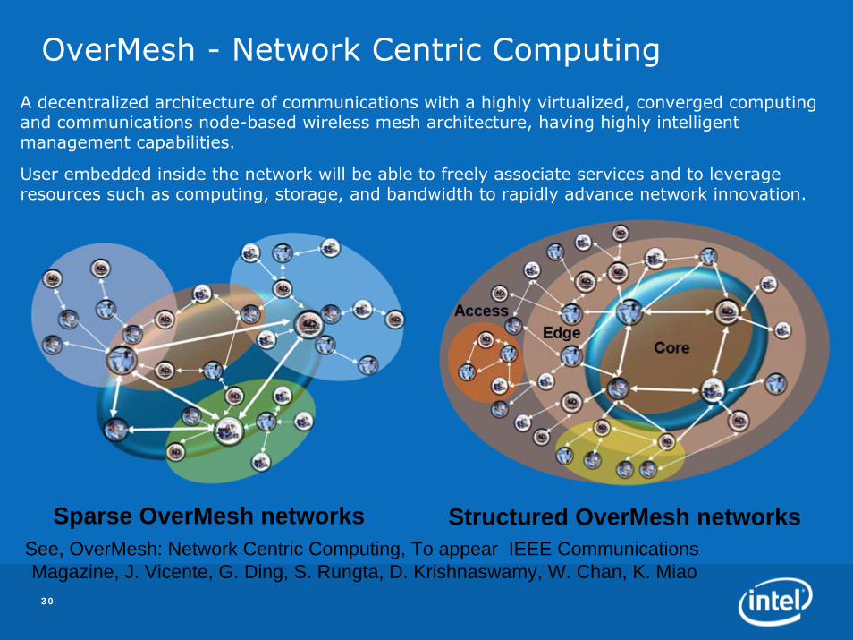
OverMesh - Network Centric Computing
A decentralized architecture of communications with a highly virtualized, converged computing and communications node-based wireless mesh architecture, having highly intelligent management capabilities.
User embedded inside the network will be able to freely associate services and to leverage resources such as computing, storage, and bandwidth to rapidly advance network innovation.
Sparse OverMesh networks Structured OverMesh networksSee, OverMesh: Network Centric Computing, To appear IEEE Communications Magazine, J. Vicente, G. Ding, S. Rungta, D. Krishnaswamy, W. Chan, K. Miao

31
Proactive Adaptive Cross-layer Cross-OverlayArchitectures
(recent research see IEEE WiMeshWorkshop, Sep 2006, Krishnaswamy et al)
32
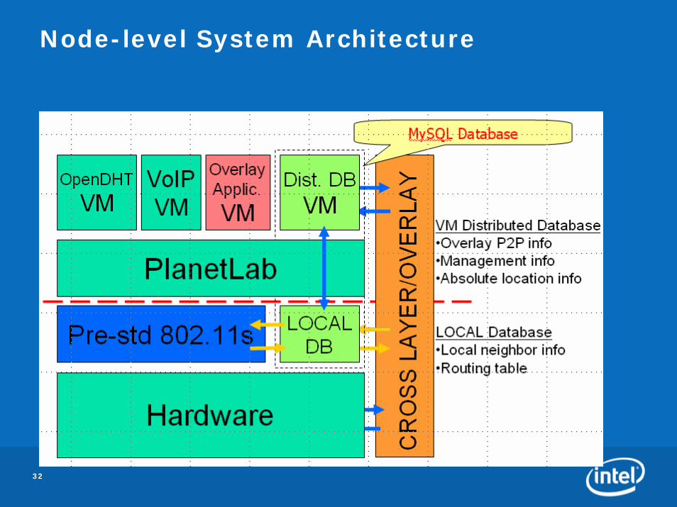
Node-level System Architecture

33
Network-aware proactive optimizations

34
Distributed Network Information Base Design

35
Application – Proactive Multi-hop L2 routing
2,
,
,
,
minimize 1
subject to
1
,
if is a n
nk
overallk r
r RouteGraph kk
k i k ki path
k ikoverallk r k
k
THdemand
ETT deadline gap
t
TH demand
f
∈
∈
⎛ ⎞⎟⎜ ⎟−⎜ ⎟⎜ ⎟⎜⎝ ⎠
≤ −
≤
≥
∑
∑
∑
onscalable application
, for all nk kpath r f∈

36
Mesh routing example

37
Mesh routing example contd. - multi-path routing

38
Simulation results – good channel PER (0.05 to 0.15)

39
Simulation results – worse channel PER (0.05 to 0.30)
40
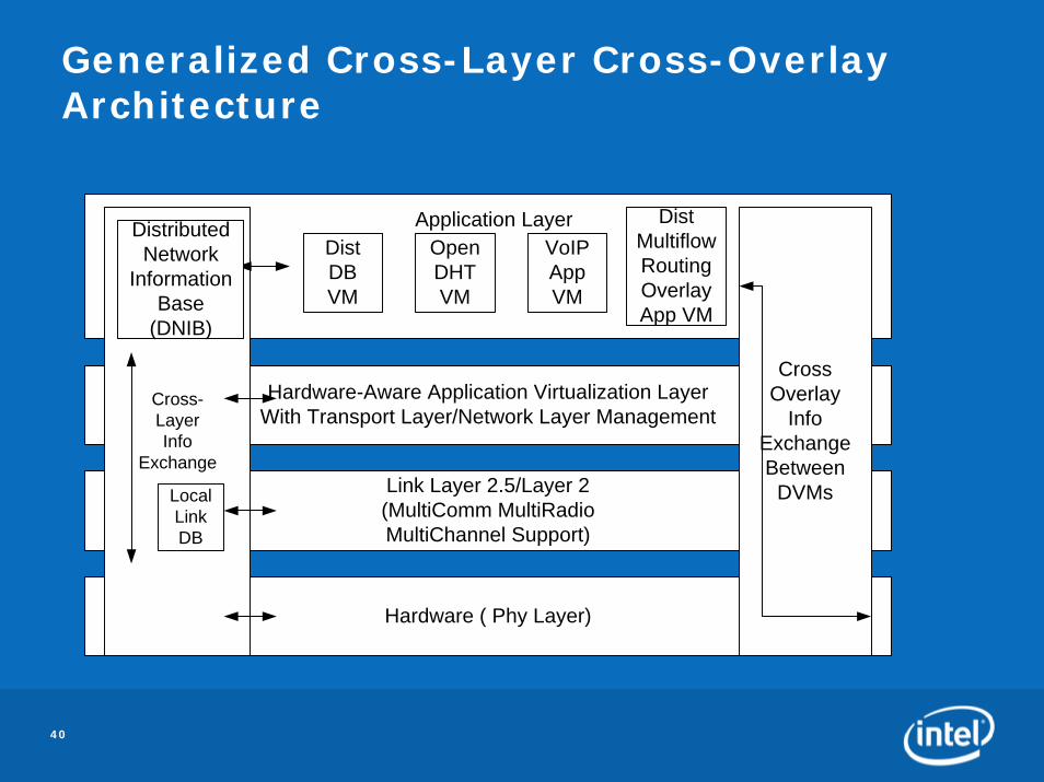
Generalized Cross-Layer Cross-Overlay Architecture
DistDBVM
DistMultiflowRoutingOverlayApp VM
VoIPAppVM
OpenDHTVM
Hardware-Aware Application Virtualization LayerWith Transport Layer/Network Layer Management
Link Layer 2.5/Layer 2 (MultiComm MultiRadio MultiChannel Support)
Hardware ( Phy Layer)
Cross-LayerInfo
Exchange
CrossOverlay
InfoExchangeBetween
DVMsLocalLinkDB
DistributedNetwork
InformationBase
(DNIB)
Application Layer

41
Example End-to-End HeterogenousNetwork Path (VoIP call)

42
Questions?
