aps march meeting 2012
TRANSCRIPT

ARPES microscopy study on free standing bilayer graphene
Po-Chun Yeh , Kevin Knox , Wencan Jin , Jerry Dadap , Philip Kim , Richard M. Osgood
Columbia UniversityAlexei Barinov, Dudin Pavel
Elettra-Sincrotrone Trieste,Italy

Outline
• Goal: To study electronic structure of free standing graphene
• Brief review of our prior monolayer graphene studies
• Bilayer – Theory and related studies– Sample preparation and apparatus– Data analysis– Comments
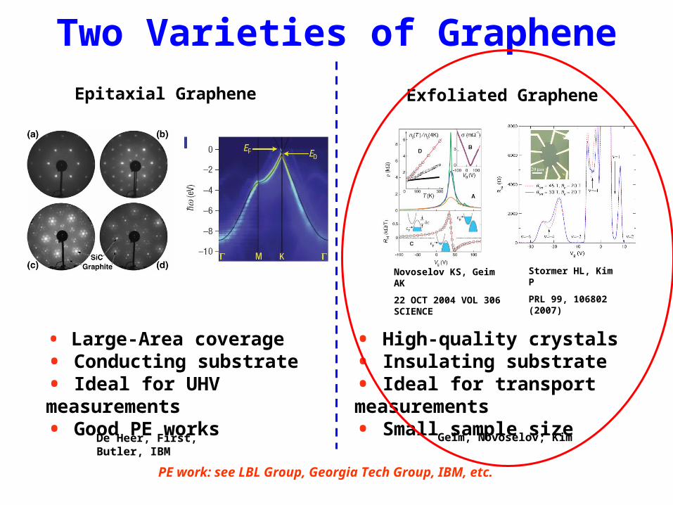
Two Varieties of Graphene
Stormer HL, Kim P
PRL 99, 106802 (2007)
Novoselov KS, Geim AK
22 OCT 2004 VOL 306 SCIENCE
Epitaxial Graphene Exfoliated Graphene
• Large-Area coverage• Conducting substrate• Ideal for UHV measurements• Good PE works
• High-quality crystals• Insulating substrate• Ideal for transport measurements• Small sample size
De Heer, First, Butler, IBM Geim, Novoselov; Kim
PE work: see LBL Group, Georgia Tech Group, IBM, etc.

For Monolayer Measurements SPELEEM Needed:For Roughness Data to Improve ARPES
SPELEEM microscope at ELETTRA
• Combines microscopy, spectroscopy
• High spatial resolution for imaging:
XPEEM (40 nm), LEEM (15 nm)
• 2 μm spot, μLEED, μARPES
• 300 meV energy resolution
• Noninvasive probe
LEEM autocorrelation
2D Roughness Parameters: ξ, w, α
=0.5
=0.3
=0.7
=0.5
=0.3
=0.7
=0.5
=0.3
=0.7
Columbia, ACSNano, 2010Columbia, ACSNano, 2010

Suspended vs Supported ARPES
ГM
K
K'
Supported Graphene
Suspended Graphene
Columbia, PRB, 2008Columbia, PRB, 2008Columbia, PRB, 2011Columbia, PRB, 2011
Our measurements show β = 0.3 fs-1eV-1
Lifetime = 1/(β*2*(E-EF)*vF) => marginal Fermi liquid
“Removing Corrugation” Yields Lifetime: Marginal Fermi Liquid
High symmetry points• No SiO2 photoelectrons• Significantly narrower peaks• Possible to measure S(k)
Removing SiO2 Interaction
10μm
Slope = β

Bilayer Graphene TheoryBilayer graphene in Bernal stacking
McCann’s Tight-binding calculation:• Weak A1B2 coupling, γ3 <<VF, negligible
• No doping or external fields•Small band asymmetry• Near K point
- L. M. Malard et al., PRB 76, 201401 (2007)
-T. Ohta et al., Science 313, 951 (2006)-S. Y. Zhou et al., Nature Materials 6, (2007)
-A.B. Kuzmenko et al., PRB 79, 115441 (2009)-C. Z. Q. Li et al., PRL 102, 037403 (2009)
-E. McCann et al., PRL 96, 086805 (2006).
Interlayer Hopping Energy
Tight-binding approach by McCann
Important works & people
Interlayer asymmetry, Δ

• 300nm thick SiO2 on intrinsic Si substrate
• No substrate doping
• Mechanical exfoliation
• Free standing on 5μm wells
• Shadow mask Au/Cr deposition, no photoresist
• Overnight thermal radiation cleaning
• Well defined layers, single domain
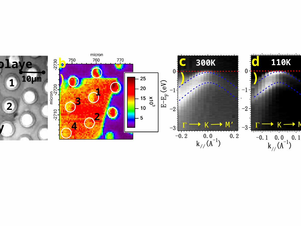
Sample Preparation
(Left) Optical microscopy image
(Right)Spatially-resolved photoemission image: angle integrated mode at 15eV electron kinetic energy, by Spectromicroscopy.
1
2
3
4
Monolayer
Bilayer
1
23
4
10μm

• Study the band structure and the Fermi surface topography
• Temperature: 110K to 300K• Beam size: 0.6 - 1μm• Photon energy: 27eV• Momentum resolution: 2.7mÅ-1
• Energy resolution: 33meV
SpectroMicroscopy at Elettra : Microscope + Monochromator
-P. Dudin et al., J. Synchrotron Rad. (2010) 17
Cryostat
Electron Analyzer
Sample
Counter
Source
Frequency selection
Schwarzschild objective
Elettra Sincrotrone, Trieste, Italy
K// (Å-1)E
-EF (
eV)
Δ, γ1
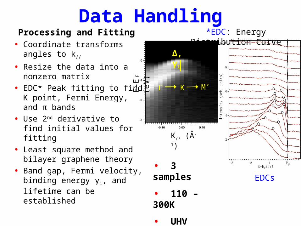
Data HandlingProcessing and Fitting
• Coordinate transforms angles to k//
• Resize the data into a nonzero matrix
• EDC* Peak fitting to find K point, Fermi Energy, and π bands
• Use 2nd derivative to find initial values for fitting
• Least square method and bilayer graphene theory
• Band gap, Fermi velocity, binding energy γ1, and lifetime can be established
• 3 samples
• 110 – 300K
• UHV
EDCs
*EDC: Energy Distribution Curve
M’K

Fermi Cutoff and Spatial Resolution
EDC*s fit at K point with Lorentzian function
convoluted with Fermi function:
T=110K
T=300K

Room temperature, 300K
2nd Derivative2nd Derivative Peak Fitting
• 2nd derivative help locates the two bands
• Parabolic – linear feature of bilayer is clear
• Dirac point is close to Fermi level within min energy resolution
• Parabolic region ~ ±0.5 Å-1
M’K
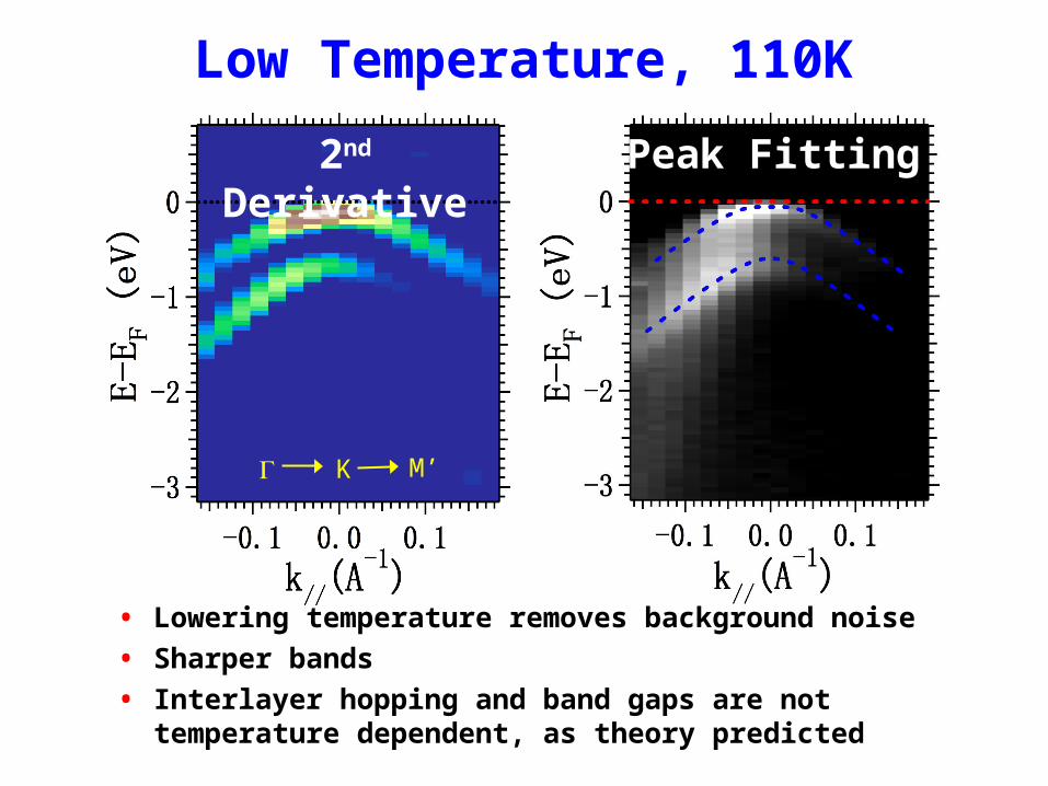
Low Temperature, 110K
Peak Fitting2nd Derivative
• Lowering temperature removes background noise
• Sharper bands
• Interlayer hopping and band gaps are not temperature dependent, as theory predicted
M’K

Results of Fitting for Exfoliated GrFit the π bands with the tight binding model:
A300K
A110K
B C D E
VF
(106 m/s)1.042±0.018
1.003±0.013
* 1.1 1 1 ~ 1.1
Δ/2 (meV)
48.0±13.4
56.2±9.4
0 40 -0.05 ~ 0.1
Variable
γ1
(eV)
0.6±0.017
0.611±0.007
0.378±0.005
0.404±0.01
0.41 ~ 0.46
0.36 ~ 0.45
A. Our ARPES measurementB. Infrared measurement on SiO2/Si, doped, 10KC. Infrared measurement on SiO2/Si, doped, 45KD. ARPES measurement on SiC, dopedE. McCann’s tight binding calculation
References:B. A.B. Kuzmenko et al., PRB 79, 115441 (2009)C. Z. Q. Li et al., PRL 102, 037403 (2009)D. T. Ohta et al., Science 313, 951 (2006)E. McCann et al., PRL 96, 086805 (2006).
* Not provided.

Summary and DirectionCharacteristics
Fermi velocity, VF
Interlayer asymmetry, Δ
Interlayer coupling, γ1
– Strain ?
– > 2ML – data looks too clean for this.
– Additional measurements
Zero-to-minimally-doped graphene measured
• Chemical doping experiments needed
• Surface corrugation and width broadening
• Band asymmetry and renormalization

Thank you

L. M. Malard et al., PRB 76, 201401 (2007)
RamanFrom graphite theory paper:
Will optical measurement changes the γ1 ?
γ1 ~0.7eV, VF = 8x10⁵
Cited by A.B. Kuzmenko et al., PRB 79, 115441 (2009), IR study
0.377eV in graphite -D.D. L. Chung, J. Mater. Sci. 37, 1475 (2002)
ARPES Lanzara’s paper: 0.35eV
We shouldn’t be looking at thin graphite, since the γ1 decreases when number of layers increases.
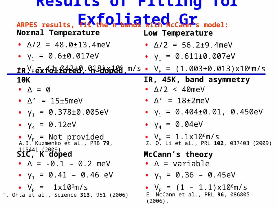
Results of Fitting for Exfoliated GrNormal Temperature
• Δ/2 = 48.0±13.4meV
• γ1 = 0.6±0.017eV
• VF = (1.042±0.018)x106 m/s
Low Temperature
• Δ/2 = 56.2±9.4meV
• γ1 = 0.611±0.007eV
• VF = (1.003±0.013)x106m/s
ARPES results, fit the π bands with McCann’s model:
• Δ = 0
• Δ’ = 15±5meV
• γ1 = 0.378±0.005eV
• γ4 = 0.12eV
• VF = Not provided
IR, exfoliated, n-doped, 10K
SiC, K doped• Δ = -0.1 – 0.2 meV
• γ1 = 0.41 – 0.46 eV
• VF = 1x10⁶m/s
• Δ = variable
• γ1 = 0.36 – 0.45eV
• VF = (1 – 1.1)x106m/s
McCann’s theory
IR, 45K, band asymmetry• Δ/2 < 40meV
• Δ’ = 18±2meV
• γ1 = 0.404±0.01, 0.450eV
• γ4 = 0.04eV
• VF = 1.1x10⁶m/sA.B. Kuzmenko et al., PRB 79, 115441 (2009) Z. Q. Li et al., PRL 102, 037403 (2009)
E. McCann et al., PRL 96, 086805 (2006).T. Ohta et al., Science 313, 951 (2006)

Bilayer graphene ARPES studies
T. Ohta et al., Science 313, 951 (2006) S. Y. Zhou et al., Nature Materials 6, (2007)
Graphene on SiC: a very specific case
Rotenberg’s Group Lanzara’s Group

Linewidth broadening• Quasiparticle's lifetime is inversely
proportional to the linewidth(FWHM) in Breit-Wigner line shape.
• Linewidth are affected by two major effects: Corrugation broadening and intrinsic broadening.
• In bilayer graphene, we should expect a mild corrugation broadening.

Corrugation Broadening • Surface roughness of the graphene sample
provides ripples with phase shift as a wave in a continuum.
• Electron scattering• Corrugation parameters: ξ, ω, and α; acquire
from LEEM and LEED measurement.• Calculation:
A~ Lorentzian, obtainable by fitting MDCs.

Intrinsic Broadening• Changes with different photon energies.• Since graphene is a 2D crystal, the valence
band initial states are highly localized along z direction – band structure is kz independent, thus it will not change with different photon energy.
• We have only one photon energy 27eV.
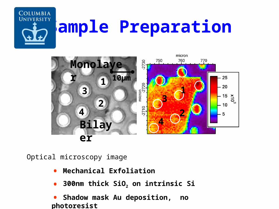
Sample Preparation
• Mechanical Exfoliation
• 300nm thick SiO2 on intrinsic Si
• Shadow mask Au deposition, no photoresist
Optical microscopy image
1
2
3
4
Monolayer
Bilayer
1
23
4
10μm

Ene
rgy
(eV
)
degree
GK
K// (Å-1)
E-E
F (eV
)
• 3 samples
• Range of temperature: 110 –300K
• UHV
Data Handling
Δ, γ1
1
2
3
4
Monolayer
Bilayer
1
2
10μm
300K 110Kb) c) d)
M’K M’K

Photoemission microscopy
Bilayer
Dispersion of trilayer measured with photon energy 74eV

Trilayer @ room temperature with photon energy 74 eV
According to the band structure, the sample is doped in the fabrication process. We can see part of the conduction band and the gap value is about 350 meV.
This is the band structure along Γ-K direction. The dispersion is strong on one side with a small tail on the other side. This is consistent with our previous theoretical calculation.