applied optoelectronics, inc.ao-inc.com/images/uploads/products/80-21-0721_akoa9...applied...
TRANSCRIPT

APPLIED OPTOELECTRONICS, INC.
QSFP+ to 4xSFP+ 40G AOC AKOA9NxxADLN0721
80-21-0721 REV A002 www.ao-inc.com © Applied Optoelectronics, Inc. 2014
Page 1 of 18
Features
Applications
Ordering Information
Form Factor Date Rate Media Distance Wavelength (nm)
Voltage (V) Coupling DDM
(Y/N) Temperature
(°C) Part Number
QSFP+ to 4xSFP+ 40G MMF 1M 850 3.3 AC/AC Y 0 ~ +70 AKOA9N01ADLN0721
QSFP+ to 4xSFP+ 40G MMF 2M 850 3.3 AC/AC Y 0 ~ +70 AKOA9N02ADLN0721
QSFP+ to 4xSFP+ 40G MMF 3M 850 3.3 AC/AC Y 0 ~ +70 AKOA9N03ADLN0721
QSFP+ to 4xSFP+ 40G MMF 5M 850 3.3 AC/AC Y 0 ~ +70 AKOA9N05ADLN0721
QSFP+ to 4xSFP+ 40G MMF 7M 850 3.3 AC/AC Y 0 ~ +70 AKOA9N07ADLN0721
QSFP+ to 4xSFP+ 40G MMF 10M 850 3.3 AC/AC Y 0 ~ +70 AKOA9N10ADLN0721
QSFP+ to 4xSFP+ 40G MMF 15M 850 3.3 AC/AC Y 0 ~ +70 AKOA9N15ADLN0721
QSFP+ to 4xSFP+ 40G MMF 20M 850 3.3 AC/AC Y 0 ~ +70 AKOA9N20ADLN0721
QSFP+ to 4xSFP+ AOC type transceiver 850nm VCSEL Laser 40Gb/s aggregated bidirectional data
throughput 1m, 2m,3m, 5m,7m, 10m, 15m, 20m
transmission with MMF 3.3V single power supply Low power consumption of max 1.5 W at
QSFP+ side. Power Level 1 compliant. Low power consumption of max 1.041 W at
SFP+ side total. Infiniband 4x QDR / 40G Base-SR4 Serial ID information support Compliant with QSFP+ MSA SFF-8436 and
SFP+ MSA SFF-8432 Compliant with RoHS Compliant with UL & TUV
40Gb/s Ethernet 40GBASE SR4‐ Infiniband QDR and DDR
interconnects Proprietary multi channel links ‐

APPLIED OPTOELECTRONICS, INC.
QSFP+ to 4xSFP+ 40G AOC AKOA9NxxADLN0721
80-21-0721 REV 002 www.ao-inc.com © Applied Optoelectronics, Inc. 2014
Page 2 of 18
Absolute Maximum Ratings
Parameter Symbol Min Max Unit Storage Temperature TS -40 +85 °C
Power Case Temperature Tc 0 70 °C
Storage Relative Humidity RH 5 85 %
Supply Voltage VCC1/ VCCTx/
VCCRx
-0.5
3.6
V
1. Limited by the fiber cable jacket, not the active ends 2. Non-condensing
Electrical Characteristics for QSFP+ side (Tc = 0 to 70 °C, VCC = 3.135 to 3.465 Volts) Parameter Symbol Min Typ Max Unit
Supply Voltage VCC1/ VCCTx/ VCCRx 3.13 3.3 3.47 V
Supply Current ICC -- -- 420 mA
Transmitter
Data Input Differential Peak-to Peak Voltage Swing(AC-Coupled) Vin,pp 200 -- 1200 mVpp
LOS Assert Threshold Vin,pp LOS 120 -- -- mV
Receiver
Data Output Differential Peak-to Peak Voltage Swing(AC-Coupled) ∆VDO pp 340 -- 650 mVpp
1. Measured with PRBS 231 –1 at 10-12 BER
Electrical Characteristics for SFP+ side (Tc = 0 to 70 °C, VCC = 3.135 to 3.465 Volts)
Parameter Symbol Min Typ Max Unit Supply Voltage VCC1/ VCCTx/ VCCRx 3.13 3.3 3.47 V
Supply Current (each) ICC -- -- 75 mA
Transmitter
Differential Input Impedance RDI 90 100 110 ohm
Data Input Differential Peak-to Peak Voltage Swing VDI 270 -- 1200 mVpp
Receiver
Differential Output Impedance RDO 90 100 110 ohm
Data Output Differential Peak-to Peak Voltage Swing(AC-Coupled)
VDO 330 -- 510 mVpp
Jitter Tolerance -- -- 0.6 -- UI
Rise / Fall Time -- 24 -- -- ps
1. Measured with PRBS 231 –1 at 10-12 BER

APPLIED OPTOELECTRONICS, INC.
QSFP+ to 4xSFP+ 40G AOC AKOA9NxxADLN0721
80-21-0721 REV 002 www.ao-inc.com © Applied Optoelectronics, Inc. 2014
Page 3 of 18
Recommended Host Board Power Supply Circuit Filter for QSFP+ side
Pin Description for QSFP+ side

APPLIED OPTOELECTRONICS, INC.
QSFP+ to 4xSFP+ 40G AOC AKOA9NxxADLN0721
80-21-0721 REV A002 www.ao-inc.com © Applied Optoelectronics, Inc. 2014
Page 4 of 18
Pin Function Definitions for QSFP+ side
Pin No. Pin Name
Symbol Function/Description
Plug Sequence Note
1 GND Ground 1 1 2 CMLI Tx2n Transmitter Inverted Data Input 3 3 CMLI Tx2p Transmitter NonInverted Data Input 3 4 GND Ground 1 1 5 CMLI Tx4n Transmitter Inverted Data Input 3 6 CMLI Tx4p Transmitter NonInverted Data Input 3 7 GND Ground 1 1 8 LVTTLI ModSelL Module Select 3 9 LVTTLI ResetL Module Reset 3
10 Vcc Rx Rx +3.3V Power Supply Receiver 2 2 11 LVCMOSI/O SCL 2wire serial interface clock 3 12 LVCMOSI/O SDA 2wire serial interface data 3 13 GND Ground 1 1 14 CMLO Rx3p Receiver NonInverted Data Output 3 15 CMLO Rx3n Receiver Inverted Data Output 3 16 GND Ground 1 1 17 CMLO Rx1p Receiver NonInverted Data Output 3 18 CMLO Rx1n Receiver Inverted Data Output 3 19 GND Ground 1 1 20 GND Ground 1 1 21 CMLO Rx2n Receiver Inverted Data Output 3 22 CMLO Rx2p Receiver NonInverted Data Output 3 23 GND Ground 1 1 24 CMLO Rx4n Receiver Inverted Data Output 3 25 CMLO Rx4p Receiver NonInverted Data Output 3 26 GND Ground 1 1 27 LVTTLO ModPrsL Module Present 3 28 LVTTLO IntL Interrupt 3 29 Vcc Tx Tx +3.3V Power supply transmitter 2 2 30 Vcc1 +3.3V +3.3V Power supply 2 2 31 LVTTLI LPMode Low Power Mode 3 32 GND Ground 1 1 33 CMLI Tx3p Transmitter NonInverted Data Input 3 34 CMLI Tx3n Transmitter Inverted Data Input 3 35 GND Ground 1 1 36 CMLI Tx1p Transmitter NonInverted Data Input 3 37 CMLI Tx1n Transmitter Inverted Data Input 3 38 GND Ground 1 1

APPLIED OPTOELECTRONICS, INC.
QSFP+ to 4xSFP+ 40G AOC AKOA9NxxADLN0721
80-21-0721 REV A002 www.ao-inc.com © Applied Optoelectronics, Inc. 2014
Page 5 of 18
1. GND is the symbol for signal and supply (power) common for the QSFP+ module. All are common within
the QSFP+ module and all module voltages are referenced to this potential unless otherwise noted. Connect these directly to the host board signal-common ground plane.
2. Vcc Rx, Vcc1 and Vcc Tx are the receiver and transmitter power supplies and shall be applied concurrently. Requirements defined for the host side of the Host Edge Card Connector are listed in Table 6. Recommended host board power supply filtering is shown in Figure 4. Vcc Rx Vcc1 and Vcc Tx may be internally connected within the QSFP+ Module module in any combination. The connector pins are each rated for a maximum current of 500 mA. This contact is an input contact with a 4.7 kΩ to 10k Ohms pull up to VccT inside the module.
APPLIED OPTOELECTRONICS, INC.
QSFP+ to 4xSFP+ 40G AOC AKOA9NxxADLN0721
80-21-0721 REV A002 www.ao-inc.com © Applied Optoelectronics, Inc. 2014
Page 6 of 18
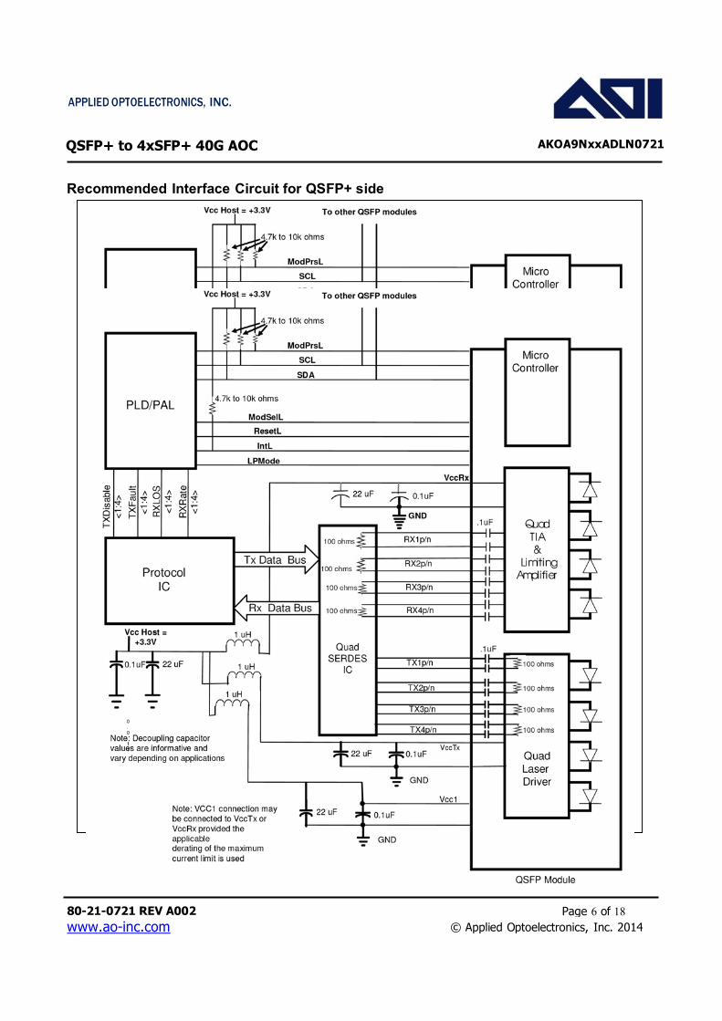
Recommended Interface Circuit for QSFP+ side

APPLIED OPTOELECTRONICS, INC.
QSFP+ to 4xSFP+ 40G AOC AKOA9NxxADLN0721
80-21-0721 REV A002 www.ao-inc.com © Applied Optoelectronics, Inc. 2014
Page 7 of 18
Pin Description for SFP+ side

APPLIED OPTOELECTRONICS, INC.
QSFP+ to 4xSFP+ 40G AOC AKOA9NxxADLN0721
80-21-0721 REV A002 www.ao-inc.com © Applied Optoelectronics, Inc. 2014
Page 8 of 18
Pin Function Definitions for SFP+ side
Pin No. Pin Name Function/Description Power Sequence Order Note
1 VeeT Transmitter Ground 1 1
2 Tx_Fault Not functional 3 2
3 Tx_Disable Not functional 3 3
4 SDA 2-wire Serial Interface Data Line (MOD-DEF2) 3 4
5 SCL 2-wire Serial Interface Clock (MOD-DEF1) 3 4
6 Mod_ABS Module Absent, connected to VeeT or VeeR in the
module 3 4
7 RS0 Rate Select 0, (not functional) 3
8 Rx_LOS Not functional 3 2
9 RS1 Not functional 3
10 VeeR Receiver Ground 1 1
11 VeeR Receiver Ground 1 1
12 RD- Receiver Inverted Data Output 3
13 RD+ Receiver Non-Inverted Data Output 3
14 VeeR Module Receiver Ground 1 1
15 VccR Receiver 3.3 V Supply 2
16 VccT Transmitter 3.3 V Supply 2
17 VeeT Transmitter Ground 1 1
18 TD+ Transmitter Non-Inverted Data Input 3
19 TD- Transmitter Inverted Data Input 3
20 VeeT Transmitter Ground 1 1
Notes:
1. The module signal ground contacts, VeeR and VeeT, should be isolated from the module case.
2. This contact is an open collector/drain output contact and shall be pulled up with a 4.7k to 10k Ohms resistor to host_Vcc on the host board. Pull ups can be connected to one of several power supplies, however the host board design shall ensure that no module contact has voltage exceeding module VccT/R + 0.5 V. Low for normal operation.
3. This contact is an input contact with a 4.7 kΩ to 10k Ohms pull up to VccT inside the module. Low for enable and High for disable.
4. This contact shall be pulled up with a 4.7k to 10k Ohms resistor to host_Vcc on the host board. Mod_ABS grounded by the module to indicate that the module is present. Mod_ABS grounded by the module to indicate that the module is present.

APPLIED OPTOELECTRONICS, INC.
QSFP+ to 4xSFP+ 40G AOC AKOA9NxxADLN0721
80-21-0721 REV A002 www.ao-inc.com © Applied Optoelectronics, Inc. 2014
Page 9 of 18
Recommended Interface Circuit for SFP+ side

APPLIED OPTOELECTRONICS, INC.
QSFP+ to 4xSFP+ 40G AOC AKOA9NxxADLN0721
80-21-0721 REV A002 www.ao-inc.com © Applied Optoelectronics, Inc. 2014
Page 10 of 18
Mechanical Diagram
APPLIED OPTOELECTRONICS, INC.
QSFP+ to 4xSFP+ 40G AOC AKOA9NxxADLN0721
80-21-0721 REV A002 www.ao-inc.com © Applied Optoelectronics, Inc. 2014
Page 11 of 18
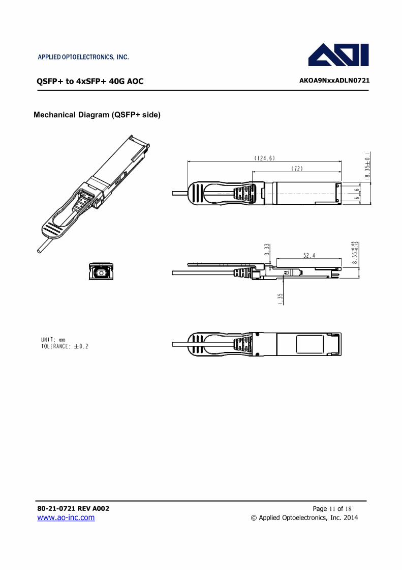
Mechanical Diagram (QSFP+ side)

APPLIED OPTOELECTRONICS, INC.
QSFP+ to 4xSFP+ 40G AOC AKOA9NxxADLN0721
80-21-0721 REV A002 www.ao-inc.com © Applied Optoelectronics, Inc. 2014
Page 12 of 18
Mechanical Diagram (SFP+ side)

APPLIED OPTOELECTRONICS, INC.
QSFP+ to 4xSFP+ 40G AOC AKOA9NxxADLN0721
80-21-0721 REV A002 www.ao-inc.com © Applied Optoelectronics, Inc. 2014
Page 13 of 18
Module Label Diagram
QSFP+ side
SFP+ side

APPLIED OPTOELECTRONICS, INC.
QSFP+ to 4xSFP+ 40G AOC AKOA9NxxADLN0721
80-21-0721 REV A002 www.ao-inc.com © Applied Optoelectronics, Inc. 2014
Page 14 of 18
EEPROM Memory A0h contents Address
AOI AKOA9NxxADLN0721 J258 xxM
Add Name of field Description ACSII HEX 0 Identifier 03:SFP or SFP “Plus” Transceiver 03
1 Ext. Identifier 04:SFP Transceiver 04
2 Connector 0B:Optical pigtail 0B
3
Transceiver
10G Ethernet 10:10G Base-SR 10
4 SONET/SDH 00
5 SONET/SDH 00
6 Ethernet 00
7 Fiber Channel 00
8 Fiber Channel 00
9 Fiber Channel 00
10 Fiber Channel 00
11 Encoding 01:8B10B, 05:SONET, 06:64B/66B 06
12 BR, Nominal 100Mbps/unit -> HEX (67:10.3125G) 67
13 Rate Identifier Rate Select 00
14 Length(9um) 1km /unit -> HEX 00
15 Length (9um) 100m /unit -> HEX 00
16 Length (50um), OM2 10m /unit -> HEX 00
17 Length (62.5um), OM1 10m /unit -> HEX xx
18 Length (Copper) 1m /unit -> HEX 00
19 Length (50 um), OM3 10m /unit -> HEX 00
20
Vendor name SFP Vendor Name (ASCII)
A 41
21 O 4F
22 I 49
23 20
24 20
25 20
26 20
27 20
28 20
29 20
30 20
31 20
32 20
33 20
34 20

APPLIED OPTOELECTRONICS, INC.
QSFP+ to 4xSFP+ 40G AOC AKOA9NxxADLN0721
80-21-0721 REV A002 www.ao-inc.com © Applied Optoelectronics, Inc. 2014
Page 15 of 18
35 20
36 Reserved Reserved 00
37
Vendor OUI SFP Vendor IEEE company ID, No ID set "00"
00
38 00
39 00
40
Vendor PN SFP Vendor Part Number (ASCII)
A 41
41 K 4B
42 O 4F
43 A 41
44 9 39
45 N 4E
46 x xx
47 x xx
48 A 41
49 D 44
50 L 4C
51 N 4E
52 0 30
53 7 37
54 2 32
55 1 31
56
Vendor rev
Hardware Revision (HEX) Ver A A 41
57 20
58 Firmware Revision (HEX) N/A
20
59 20
60 Wavelength 1nm /unit -> HEX 0352:850nm
xx
61 xx
62 Reserved xx
63 CC_BASE Check Sum 0 to 62 byte xx
64 Options
00
65 18:TX-DIS,TX_Fault 1A:TX-DIS,TX_Fault,RX-LOS 00
66 BR, max 1% /unit 00
67 BR, min 1% /unit 00
68
Vendor SN Vendor SN (ASCII)
XX
69 XX
70 XX
71 XX
72 XX

APPLIED OPTOELECTRONICS, INC.
QSFP+ to 4xSFP+ 40G AOC AKOA9NxxADLN0721
80-21-0721 REV A002 www.ao-inc.com © Applied Optoelectronics, Inc. 2014
Page 16 of 18
73 XX
74 XX
75 XX
76 XX
77 XX
78 XX
79 XX
80 XX
81 XX
82 XX
83 XX
84
Date code
Year (ASCII) XX
85 XX
86 Month (ASCII)
XX
87 XX
88 Day (ASCII)
XX
89 XX
90 Blank
20
91 20
92 Diagnostic Monitoring Type 00:W/O DDM, 58:W/I DDM(Ext_Cal), 68:W/I DDM(Int_Cal)
00
93 Enhanced Options E0:A/W, Tx_Dis, Tx_fault F0:A/W, Tx_Dis, Tx_fault, Rx_LOS B0:A/W, Tx_fault, Rx_LOS
00
94 SFF-8472 Compliance 01:9.3, 02:9.5 04:10.4 05:11.0 05
95 CC_EXT Check Sum 64 to 94 byte XX
96
Read-only
Vendor name : AOI (PM suggest)
A 41
97 O 4F
98 I 49
99 20
100 20
101
Define cable length, unit: 0.1m EX: 123.4m (wxy.z)
w=0x01, x=0x02, y=0x03, z=0x04
w xx
102 x xx
103 y xx
104 z xx
105
Reserved
00
106 00
107 00
108 00
109 00

APPLIED OPTOELECTRONICS, INC.
QSFP+ to 4xSFP+ 40G AOC AKOA9NxxADLN0721
80-21-0721 REV A002 www.ao-inc.com © Applied Optoelectronics, Inc. 2014
Page 17 of 18
110 00
111 00
112 00
113 00
114 00
115 00
116 00
117 00
118 00
119 00
120 00
121 00
122 00
123 00
124 00
125 00
126 00
127 00
128-255 Read-only Read-only
00
APPLIED OPTOELECTRONICS, INC.
QSFP+ to 4xSFP+ 40G AOC AKOA9NxxADLN0721
80-21-0721 REV A002 www.ao-inc.com © Applied Optoelectronics, Inc. 2014
Page 18 of 18
Regulatory Compliance
Item Standard
Electromagnetic Interference (EMI)
FCC Part 15 Class B EN55022 Class B (CISPR 22B) VCCI Class B
ESD (Module case) Contact Discharge EN61000-4-2 criterion B ESD (Module case) Air Discharge EN61000-4-2 criterion B ESD (Electrical connector) JEDEC JESD22-A114-B RoHS 2011/65/EU Laser Eye Safety FDA 21CFR 1040.10 and 1040.11 Component Recognition UL and TUV
Laser Safety Information All versions of this laser are Class 1 laser products per IEC1/EN2 60825-1. Users should observe safety precautions such as those recommended by ANSI3 Z136.1, ANSI Z36.2 and IEC 60825-1.
This product conforms to FDA (CDRH) 21 CFR 1040.10 and 1040.11 except for deviations of laser safety class designation pursuant to 'Laser Notice No.50'.
Product labeling:
If labeling is not affixed to the module due to size constraints; then rather, labeling is placed on the outside of the shipping box. This product is not shipped with a power supply. Caution: use of controls or adjustments or performance of procedures other than those specified herein may result in hazardous radiation exposure.
Certifications
UL 60950-1 (E243407) TUV EN60950-1, EN 60825-1, EN 60825-2
Documentation is available upon request. (1) IEC is a registered trademark of the International Electrotechnical Commission (2) Within Europe the IEC standard has been adopted as a European Normative standard known as EN 60825, and each European country will have its own version of this standard, for example, the British Standards version known as BS EN 60825. There can be small differences between the different countries versions of EN 60825, and these are in part caused by the process of translating the standard into the native language of that country. (3) ANSI is a registered trademark of the American National Standards Institute Note: All information contained in this document is subject to change without notice.
Class 1 Laser Product Compliance with 21 CFR 1040.10 and 1040.11