applications handbook -...
TRANSCRIPT

© Copyright 2013 United Electronic Industries, Inc. All rights reserved.
ApplicationsHandbook
Data Acquisition, Embedded I/O
and Control

i
® United Electronics IndustriesApplications Handbook
Version: 1.0 — December 2013© 2013 United Electronic Industries, Inc.
508-921-4600www.ueidaq.com
Introduction
About UsUEI is a leader in the PC/Ethernet data acquisition and control, Data Logger/Recorder and Pro-grammable Automation Controller (PAC) and Modbus TCP markets. Our revolutionary “Cube” form factor provides a compact, rugged platform, ideal for applications in the automotive, aerospace, petroleum/refining, simulation, semiconductor manufacturing, medical, HVAC, and power generation fields—and more.
The Cube is uniquely flexible, capable of being deployed as an Ethernet I/O slave, a stan-dalone data logger, a standalone Linux-based PAC or a Modbus Slave. The “Cube” also offers incredible I/O flexibility, accommodating up to 6 I/O boards from a selection of over 25. This allows you to precisely match the I/O configuration to your application. With I/O interfaces for analog I/O, digital I/O, counter/timer, ARINC-429, quadrature encoder, CAN-bus, serial I/O and more, we are sure to have the interface you need.
We also offer an extensive array of PCI and PXI data acquisition and control boards. With the world’s widest selection of simultaneously sampling A/D boards and the worlds most dense analog output boards (up to 96 channels per slot!) UEI is sure to have just what your board-level DAQ application requires.
UEI supports all popular Windows, Vista, Linux and Real-time operating systems and program-ming languages. We also offer complete and seamless support of all major application pack-ages, including LabVIEW, MATLAB and DASYLab.
We are committed to providing the highest quality hardware, software and services, enabling engineers and scientists worldwide to interface data-acquisition and control hardware to the real world. Using state-of-the-art technologies, we serve the needs of individual researchers/developers, systems integrators and OEMs.
We pride ourselves on listening to our customers, responding to their needs with stand-ard products and variations thereof in a timely fashion so they can complete their systems successfully, on time, and within budget. We strive to provide a pleasant, enthusiastic work environment where we foster creativity at all levels and provide opportunities for professional and personal growth.
Our staff exercises its creativity to find innovative solutions for our customers, thus ensuring growth and prosperity for UEI, our employees, and our customers.
InnovationsLinux Support—Even for Real Time ExtensionsOnly a very few select firms offer professionally developed, fully supported Linux data-acq drivers that give programmers access to all on-board hardware functions. UEI is a leading figure in this trend. Our drivers are compatible with all major Linux distributions. In addition, these drivers work with the realtime extensions available from FSMLabs and RTAI. Thus, you can develop a hard realtime system and get away from all the problems associated with reli-ability under Windows.
LabVIEW for LinuxUsing our experience with Linux drivers, we were the first firm to offer support software that allows you to collect data directly into LabVIEW for Linux—something that nobody else offers, not even the developer of LabVIEW itself! With our drop-in replacement VIs, you can port a
iiIntroduction
® United Electronics IndustriesApplications Handbook
Version: 1.0 — December 2013© 2013 United Electronic Industries, Inc.
508-921-4600www.ueidaq.com
data acquisition application running under Windows on NI hardware to Linux (or, even better, Real Time Linux) on UEI hardware in a matter of minutes.
Real Time SupportAs you’ve already seen, we support Real Time Linux, but that’s not where our support for realtime development stops. We’re also proud to offer a driver compatible with QNX, one of the premier RTOSs on the market. We’re constantly expanding our realtime support, so call to see if we’ve now got drivers for your favorite RTOS.
Multithreaded NT Driver with SMP SupportOf course, we support every common version of Windows. However, our software development group took the time to write a driver that is optimized for Windows NT and 2000 and so takes full advantage of those environments’ potential. For instance, even on a single-CPU system the software allows multiple I/O subsystems to execute concurrently. If some idle time comes up in a task, it doesn’t wait for completion but rather immediately passes control to other tasks. This multithreading also means you can run multiple boards at high throughput rates concurrently. And in symmetrical multiprocessing (SMP) systems this driver can automatically distribute tasks to the various CPUs without user intervention.
Support for Every Major Test-Development EnvironmentBeyond LabVIEW—where our drop-in replacement VIs are available for both Linux and Win-dows—we support all major test environments. Our latest additions are MATLAB, SIMULINK and xPC from The MathWorks. Of course, you’ll find drivers for your old friends: Agilent VEE, DASYLab, DIAdem and TestPoint.
PowerDAQ Capabilities on PXIThis document details some of the great hardware/software advances we’ve made with our PCI-based PowerDAQ family. Even better, we’ve taken this power and moved it over to the PXI platform in our PDXI family. Thus you get a familiar software environment, but the PCI bus takes on a new ruggedized form. But with UEI moving to PXI means no limitations in performance.
DSP Powered PCI InterfaceIt’s easy to put a commercial PCI-interface chip on a data-acq board, but performance often suffers because those devices aren’t optimized for test and measurement. We started with a Motorola DSP chip, which features an integral burst mode bus-mastering PCI interface and six high-speed DMA channels. We then wrote specialized firmware that ties our I/O subsystems tightly into the bus interface. We also integrated performance-boosting hardware resources. Our design strategy was to optimize the load among all these resources, including the DSP, so the board could sustain a high level of performance while reducing the load other boards typically place on the host PC’s CPU. The result? The board moves analog and digital data at ex-tremely high rates unachievable with conventional devices and techniques, and it easily keeps up with our fastest 1.25 MS/s multifunction boards.
Simultaneous Operation of all SubsystemsMost data acquisition boards provide multiple subsystems to handle analog inputs, analog out-puts, digital I/O and counter/timers. Most vendors also claim that these subsystems can all run at the same time, but beware! In many cases subsystems must share resources such as timers or DMA channels and in reality can’t all be run together. PowerDAQ boards, in contrast, incorpo-rate a DSP along with system timing control logic and other resources that allow all subsystems to run concurrently at high speeds.
iiiIntroduction
® United Electronics IndustriesApplications Handbook
Version: 1.0 — December 2013© 2013 United Electronic Industries, Inc.
508-921-4600www.ueidaq.com
Custom Front-End Instrumentation AmplifierMost data-acq boards use low-cost commercial programmable-gain amplifiers in their analog front ends. In applications when multiple channels operate at different gains, though, they gen-erally require you to drop the sampling rate from peak-rated speed. We solved that problem by carefully selecting components for a custom instrumentation amplifier that achieves wide bandwidth at high gains with low harmonic distortion. This approach also allows us to optimize the front end for each member of the PowerDAQ family. As a result you pay no throughput or accuracy penalties when performing multichannel acquisition with different gains-even at peak speeds.
Highest Effective Number of BitsPowerDAQ is optimized both for DC and AC measurements. Our engineers performed exten-sive research and testing of components and circuits designs. Using only highest grade devices in the industry with low noise and distortion, low non-linearity and high slew rate, we approach the very edge of the theoretical limit for the maximum effective number of bits (ENOBs). We designed and optimized every stage of the analog signal path to eliminate static and dynamic inaccuracies. Resistors, capacitors and their locations had been chosen to minimize noise and distortion introduced by passive elements. Our analog circuitry is also powered separately us-ing a well-filtered and ultra-clean DC/DC converter.
Simultaneous Sampling with Variable GainsSome applications demand true simultaneous sampling across multiple channels. On the PCI bus, UEI offers the most power. True, you can find PCI boards with several A/Ds or purchase external SSH units. In contrast, we pack our SSH boards with as many as eight sample/hold amps. That fact means that you can sample each channel at a different gain and set its input range independent of the others. Nobody else offers this level of flexibility on a PCI-bus board along with the tight timing possible only with onboard solutions and without the expense of external accessories.
High-Density ModelsIn many systems, the number of slots available for I/O cards is limited. We recognize this fact and have designed models of our various card families with unusually high densities. In fact, we believe that in some cases you won’t find this many channels on any competitive products. For instance, can you find 96 independent D/A converters on one PCI card anywhere else? We doubt it! And how about 128 digital I/O points on a card. As an aside, note that a special model of our digital I/O cards can sink as much as 90 mA per channel – far beyond the 20 mA that’s typical for this class of card.
Ultra-Low-Noise PC-Board DesignTo achieve the level of performance just mentioned, we’ve also taken great pains during board layout. We started with top-quality components and worked closely with the engineering de-partments of chip vendors to learn about the tricks and techniques not listed in any app notes or data sheets. We paid special attention to the placement of each device on a 6-layer board that separates analog and digital lines with power and ground planes. To even further reduce digital noise, we chose to operate the DSP and high-speed logic at 3.3V.
Advanced Circular BufferModern drivers for data-acq boards eliminate many low-level jobs you had to perform in the DOS days to collect data. Today, for instance, one or two commands generally suffice to digitize a waveform and store results to a buffer in system RAM. Note, though, that with most drivers you have no access to any of the data until the buffer is completely full and the driver releases it to the application. Large buffers increase efficiency of data-transfer across the system bus, but

ivIntroduction
® United Electronics IndustriesApplications Handbook
Version: 1.0 — December 2013© 2013 United Electronic Industries, Inc.
508-921-4600www.ueidaq.com
the tradeoff is longer waiting time to access each point. With extensive experience developing Windows drivers, UEI’s software engineers designed a driver mechanism that provides opti-mal performance yet gives an application immediate access to any data in the buffer. There’s no longer any need for the application to wait for the buffer to fill. And to let your application know the moment new datapoints are ready for analysis and plotting, the driver’s event-notification mechanism tells you that it’s moved a scan or frame of data into the buffer. Now real-time plots update faster and smoother than ever before and real-time analysis routines can actually run in real time.
Continuous Gap-Free Streaming to DiskThere are boards with fast A/D’s available. Not only can we give you a fast A/D, but the Pow-erDAQ can also stream the raw data to the disk without dropping a bit as long as your disk has room. Better yet, you can stream high-speed data from as many as four boards all at the same time, without losing a single sample. We’ve achieved this feat thanks to our unique DSP-based PCI-bus interface as well as our optimized hardware designs, firmware and driver innovations.
Multiboard Interrupt SharingEven with today’s systems, interrupts are a scarce commodity. In theory, any board designed to adhere closely to the PCI specs and supplied with a properly written Windows NT driver can share system interrupts with any other PCI-bus boards. In practice, though, you’d be surprised at the number of vendors who warn against sharing interrupts among their boards. UEI isn’t one of them – we’ve designed our hardware and software to support interrupt sharing among multiple PowerDAQ boards and other properly implemented PCI boards on the same mother-board, and we’ve run extensive tests to ensure their proper operation under all conditions.
Preassigned Power-On Output States; Interrupts on Digital InputsOn PowerDAQ boards, digital outputs always assume a user-defined state when you apply power. This situation is in stark contrast to boards that use low-cost 8255 chips to implement digital I/O; you can’t predict if digital outputs will come up in the High or Low state-an obvious-ly dangerous condition. In addition, eight of our digital inputs feed high-speed edge-detection logic that asserts an interrupt. User code can determine which of the eight lines did so and run the appropriate routine.
Calibration Across All Ranges and GainsWhen they calibrate their boards, vendors typically work with only one input range at unity gain; they assume other settings likewise meet spec. Other vendors calibrate products only at the component level. At UEI we start by using NIST-traceable equipment to calibrate our boards as complete systems, accounting for every portion of the analog signal path including interface cables. There’s no twiddling of pots because the boards employ onboard DACs whose calibra-tion values reside in an onboard EEPROM. Finally, each board ships with a Calibration Certificate that attests that it’s passed an examination of each I/O subsystem on every channel and every gain/range.
Counter/Timers Always Available to Users, Easy to ProgramData-acq board designers typically use an 82C54 or some derivative to supply the counter/timers necessary to pace analog or digital I/O operations. Sometimes these counter/timers are dedicated to these I/O operations and are not available to the user. Or, maybe the user must choose between using them as counters or to run analog I/O or digital I/O. No such limita-tions exist on PowerDAQ family boards; the DSP timers handle all I/O pacing, so the onboard 82C54 is always dedicated exclusively to user applications. Programming the three counter/

vIntroduction
® United Electronics IndustriesApplications Handbook
Version: 1.0 — December 2013© 2013 United Electronic Industries, Inc.
508-921-4600www.ueidaq.com
timers is also far easier. Most boards simply bring out lines that connect to the counter/timers’ control signals and output, and you have to hardwire them to signal sources and destinations. Instead, we provide a matrix switch that allows you to configure these signals completely under software control. For the clock input you can select a software strobe, internal hardware clock, a cascaded signal from another counter or an external source. You can also set the gate either from software or an external signal, and you can also read the device’s output through soft-ware. Additionally, each of the three counters can generate an interrupt on terminal count.
Extensive Triggering and ClockingNobody in the industry offers a wider variety of triggering and clocking capabilities, which we’ve implemented in the custom system timing/control logic. PowerDAQ boards feature two clocks: the first, a sample or pacer clock, starts individual conversions; the second, a channel-list or burst clock, initiates passes through the channel/gain list. Either can run from an internal hardware or software source as well as an external trigger line, using either rising or falling edg-es. We supply a separate input line for each of these two clocking signals. High-speed digital circuitry virtually eliminates aperture delay. You can also synchronize multiple cards in the same chassis or in separate PCs to the same clocks. Finally, we offer hardware-based synchronization between the burst clock and the I/O subsystems. Thus you can implement a stimulus/response setup with a predictable latency, a feat impossible when coordinating these two activities through software under Windows. Together, these two clocks allow you to acquire data from a number of channels with one time period between them, and then wait a different time period before doing it all over again. This implements burst mode with both programmable conver-sion rate and a programmable burst rate.
Flexible Acquisition Timing with “Slow Bits”It’s not unusual to find boards with channel/gain lists, but for the ultimate in flexibility, UEI allows you to do plenty with the 256-entry list on PowerDAQ boards. For instance, the same channel can appear multiple times in the list, effectively changing its sampling rate compared to the others. In addition, we give you more control over individual channels beyond selecting their order and gain. For example, you can increase the acquisition time for just one channel so as to ensure accuracy at high gains, or to work with a sluggish sensor – without slowing down all the others. To do so, you insert a Slow Bit, which adds a user-configurable delay after a particular entry.
Sophisticated Digital I/O CardsIt’s easy to knock out a digital I/O board using an 8255 or equivalent chips, but do not expect high-speed performance. Using the same DSP technology as our multifunction cards, our digital I/O cards work with 16-bit line drivers that allow you to configure startup states. Also thanks to the DSP, you can employ three counter/timers, four 100 nsec interrupt lines and two Enhanced Synchronous Serial Interfaces that ease interfacing to codecs and other telecom-related devices with high-speed serial I/O streams, a feature you’ll not find elsewhere. Again, as with analog inputs, you can stream digital values to memory or disk at high rates.
Tech Support & Warranty All hardware manufactured by UEI is warranted for two years to the original purchaser. Any product that fails will be repaired or replaced with the same or similar device, at the discretion of UEI. Warranty may be extended at the time of purchase to five years for 10% of a product’s cost. Technical support via telephone/email is free to all UEI customers. The latest revision of our software is available free of charge and may be downloaded from our web site.
viIntroduction
® United Electronics IndustriesApplications Handbook
Version: 1.0 — December 2013© 2013 United Electronic Industries, Inc.
508-921-4600www.ueidaq.com
10-Year AvailabilityUEI guarantees the availability of all RACKtangle®, Cube, and FLATRACK™ series products(including DNA, DNR, UEIPAC, UEISIM, UEILogger and UEIModbus chassis and compat-ible I/O boards, manufactured by UEI) for a minimum of 10 years. Unless you are specifically notified at the time of purchase, all DNA/DNR series products purchased will be available for purchase for at least 10 years. We understand the investment you make by using our products and we ensure long-term product availability. Protecting customers from product obsolescence issues is nothing new at UEI. We still sell ISA bus boards. Now our excellent long-term support is backed up by our written promise. ALL RACK, Cube, and FLATRACK series products in the catalog will be available for 10+ years!
10-Year Availability Guarantee
Here’s how the program works. Purchase any UEI product or products starting with: DNA, DNR, UEIPAC, UEILogger, UEISIM, or UEIModbus. We will confirm your order immediately. If we do not specifically mention in our confirmation that one (or more) of the products in the order is excluded from our 10-year availability guarantee then all products are covered. What this means is that for 10 years from the date of the order, we guarantee that you can purchase the products.
There are no quantity restrictions on the guarantee. For example, if on January 11, 2014 you place an order for:
Qty. Product
1 DNA-PPC8
3 DNA-AI-207
2 DNR-12-1G
5 DNR-DIO-448
We will confirm the order. If we do not state in the order confirmation that one or more of these products is not covered by our 10-year availability guarantee then the guarantee is in place. This means we guarantee that up until January 10, 2024v, you may place an order for any or all of these products. There are no quantity restrictions on the number of units you purchase at any time during the 10-year period. Should we note that any product is no longer covered by the 10-year guarantee, we will provide a last time buy date.
We know that during the 10-year period, UEI is likely to face obsolescence on various com-ponents used in our many products. If and when this happens we will redesign the products as required to maintain product availability. Part of the Guarantee is that if we are required to perform such a redesign, we promise that all products are fully hardware and software back-ward compatible with their original designs. This compatibility includes all performance and functional specs, all dimensions and weights, connector pin-outs, etc.

viiIntroduction
® United Electronics IndustriesApplications Handbook
Version: 1.0 — December 2013© 2013 United Electronic Industries, Inc.
508-921-4600www.ueidaq.com
Contact UsAddressUnited Electronic Industries, Inc.27 Renmar AvenueWalpole, MA 02081
Phone NumbersTel: (508) 921-4600Fax: (508) 668-2350
[email protected]@[email protected]@ueidaq.com
Directions from Logan Airport
HotelsPreferred:Four Points1125 Boston Providence TurnpikeNorwood, MA(781) 769-7900
Closest: Best Western Plus/ The Inn at Sharon/Foxboro395 Old Post RdSharon, MA(781) 784-1000
Next Closest: Renaissance Hotel 28 Patriot Place Foxborough, MA
Alternatives:Courtyard by Marriot300 River Ridge Drive Norwood, MA781-762-4700
Hampton Inn434 Providence Highway Norwood, MA781-769-7000

viii
® United Electronics IndustriesApplications Handbook
Version: 1.0 — December 2013© 2013 United Electronic Industries, Inc.
508-921-4600www.ueidaq.com
Contents—Applications Handbook
Introduction ..................................................................................................................................... iAbout Us .................................................................................................................................................................. iInnovations ............................................................................................................................................................. iTech Support & Warranty .................................................................................................................................v10-Year Availability .............................................................................................................................................viContact Us ........................................................................................................................................................... vii
1 Everything You Ever Wanted To Know About Data Acquisition and Embedded Control .... xiPart 1—Analog Inputs .......................................................................................................................................1Part 2—“Other” types of DAQ I/O Hardware .......................................................................................... 37
2 Design Notes ............................................................................................................................. 50Board Versus Box: The Age-Old DAQ Dilemma ...........................................................................50A Modern Alternative to Reflective Memory and VME ....................................................................... 53Real-Time Extensions for Linux .................................................................................................................... 63How to Design Linux Device Drivers for Data-Acquisition Boards—Part 1 ................................. 77How to Design Linux Device Drivers for Data-Acquisition Boards—Part 2 ................................. 88
3 Application Briefs ..................................................................................................................... 96COLBERT Treadmill for NASA Space Station Uses UEIPAC ................................................................. 96M+P International Uses PowerDNA Cubes to Monitor Power PVlant Pipe .................................. 97FlightSafety International’s RACKtangle-Based Sim I/O ..................................................................... 99Rocket Test Stand with PowerDNA Cube and AI-225 ........................................................................105Strain Gage Measurement with AI-208 Using DASYLab and LabVIEW .......................................107Thermocouple Measurement with AI-225 Using DASYLab and .NET .........................................116Using Accelerometers in a Data Acquisition System .........................................................................123Advanced In-Flight Data Recorder ...........................................................................................................130PowerDNA Hardware at Tinker Air Force Base .....................................................................................134How Orbital Uses PowerDNA Cubes in Ground Support System .................................................139Using PowerDNA Fiber-optic Based Cubes in Bridges and Structural Testing .........................147Unmanned Land Vehicle Unmanned Land Vehicle Controller Uses UEIPAC ............................148Data Logging in Heavy, Off-Road Trucks ................................................................................................150Aircraft Flight Testing Using UEILogger ..................................................................................................152Appliance Maker Automates Temperature Measurement Test Stand .........................................155Landing Gear Strain Measurement for Mars Landing Vehicle ........................................................157Using the PowerDNA UEILogger in a Cellular Wireless Network...................................................159High Channel Count Ethernet link makes distributed I/O cube perfect for testing large structure ............................................................................................................163Flexible Waveform Generation Accomplishes Safe Braking ...........................................................165Data-Acquisition Drivers for Real-Time OS Ease Research into Ocean-Fishery Management ......................................................................................................................169Digital I/O Card Counts DNA Fragments in Nano Biotechnology System .................................173
4 A Glossary of Terms Commonly Used In Data Acquisition and Control ............................. 176

ix
® United Electronics IndustriesApplications Handbook
Version: 1.0 — December 2013© 2013 United Electronic Industries, Inc.
508-921-4600www.ueidaq.com
1 Everything You Ever Wanted To Know About Data Acquisition and Embedded Control By Bob Judd
Abstract of ArticleThis article is comprised of two parts. Chapter 1 was designed to introduce the key aspects of computer-based data acquisition and control to new users. It can also serve as a useful refer-ence document for existing DAQ customers. Chapter 1, “Analog Inputs”, covers a myriad of top-ics related to making measurements with a computer.
Chapter 2, “‘Other’ types of DAQ I/O Hardware”, covers devices such as Motion I/O, Synchro/Resolvers, LVDT/RVDTs, String Pots, Quadrature Encoders, and Piezoelectric Crystal Controllers. It also includes a discussion of Analog Outputs, Digital Inputs, Digital Outputs, Counter/Timers, and Special DAQ functions, covering such topics as communications interfaces, timing, and synchronization functions.
Chapter 2 is about measurement types and system requirements other than the standard A/D, D/A, and DIO. Though most channels are included in the “big three”, most systems also have a few channels of “other, less common” types. Whether you call them “special” or “oddball” or “less common”, the reality of addressing these channels is often the most difficult and challenging part of building the DAQ system. For successful system implementation, these special channels must be addressed — since a ninety five percent solution is not an option.
The vast majority of data acquisition and control I/O channels are fairly standard types: Analog Inputs (a.k.a. A/D), Analog Outputs (a.k.a. D/A), and parallel Digital I/O. System requirements vary greatly regarding sample rates, accuracy /resolution requirements, output capabilities, and the like. These considerations are far from trivial, and much has already been written about them.
The non-mainstream I/O channels include such hardware devices as: Synchro/Resolver inputs, LVDT/RVDT inputs, Quadrature Encoders, and Pulse Width Modulated outputs. Communica-tions interfaces to such common buses as RS-232, RS-485, CAN, ARINC 429, MIL-STD-1553, plus timing/synchronization considerations are discussed in Chapter 2. The article provides an intro-duction to many of these interfaces, explains how they work, and describes the factors/features you should either demand or not allow in your design.
Although most data acquisition and control I/O channels are fairly common types, system requirements vary greatly. The old 80-20 rule, however, holds as well in the DAQ arena as anywhere. Eighty percent of the I/O channels are typically addressed by twenty percent of the available I/O products. Since nobody wants an eighty percent solution, however, the remaining twenty percent of the I/O channels must also be addressed. Chapter 2 of this article, therefore, provides a brief introduction to the “other, less common” I/O types and also offers some things to look for (and watch out for) while specifying these products.
Author BiographyBob Judd has been involved in the PC-based DAQ market for over twenty years. Currently Director of Sales and Marketing at United Electronic Industries (UEI), he has served as General Manager, Vice President of Marketing, and Vice President of Hardware Engineering at Measure-ment Computing. Bob was also Vice President of Marketing at industry pioneer MetraByte. He holds a Bachelor’s degree in Engineering from Brown University and a Master’s degree in management from MIT.
Editor’s NoteThis document does not contain complete descriptions of any of the topics. The goal of this document is only to provide a general understanding of each topic. More detailed investiga-tions can then be initiated in areas where more detail is required or desired.

x
® United Electronics IndustriesApplications Handbook
Version: 1.0 — December 2013© 2013 United Electronic Industries, Inc.
508-921-4600www.ueidaq.com
Contents—Everything You Ever Wanted To Know About Data Acquisition and Embedded Control
1.1 Preamble .................................................... 1 1.2 Introduction .............................................. 1 1.3 Data Acquisition, Data
Logging & Control ................................... 2 1.3.1 Data Logging ............................................ 2 1.3.2 Data Recording ........................................ 2 1.3.3 “— & Control” ........................................... 3 1.4 Board- vs. Box-based Systems ............ 3 1.5 Tradeoffs and Considerations ............. 3 1.5.1 Distance from the PC to the
Sensor or Measurement ........................ 3 1.5.2 Portability .................................................. 3 1.5.3 Number of I/O Channels ....................... 4 1.5.4 PC Obsolescence ..................................... 4 1.5.5 Preferred Host Computer ..................... 4 1.5.6 Price ............................................................. 4 1.5.7 Pure Speed ................................................ 4 1.6 Popular PC Interfaces ............................ 4 1.6.1 Ethernet (100Base-T) ............................. 4 1.6.2 Gigabit Ethernet (1000Base-T) ........... 5 1.6.3 Fiber Ethernet (100Base-FX) ............... 5 1.6.4 Firewire (IEEE-1394a and b) ................. 5 1.6.5 GPIB (IEEE-488) ......................................... 6 1.6.6 PCI (Peripheral Component
Interconnect) Bus ..................................... 6 1.6.7 PCI Express ................................................ 6 1.6.8 PCI-X ............................................................ 7 1.6.9 PXI ................................................................. 7 1.6.10 PXI Express ................................................. 7 1.6.11 RS-232 ......................................................... 7 1.6.12 RS-422/485 ................................................ 8 1.6.13 USB ............................................................... 8 1.6.14 Wireless ....................................................... 8 1.7 Analog Inputs ........................................... 8 1.8 A/D Converters ........................................ 9 1.8.1 Resolution .................................................. 9 1.8.2 A/D Converter Types .............................. 9 1.8.3 Successive Approximation ................10 1.8.4 Sigma Delta .............................................10 1.8.5 Flash ...........................................................10 1.8.6 Dual Slope / Integrating .....................10 1.9 Input Channel Configuration ............11 1.10 Simultaneous Sampling .....................12 1.11 Accuracy Specifications ......................13 1.11.1 Input Offset .............................................14
1.11.2 Gain Error .................................................14 1.11.3 Non-Linearity ..........................................14 1.11.4 Noise ..........................................................15 1.11.5 Calculate the Total Error ......................15 1.12 Sample Rate ............................................15 1.12.1 How fast is fast enough? ....................15 1.13 DAQ “System” Considerations ...........16 1.14 Input Range ............................................18 1.15 Differential and Single-ended
Inputs ........................................................18 1.15.1 Differential Mode Advantages .........18 1.15.2 Common Mode and CMRR ................19 1.15.3 Connecting to a
Differential Input ...................................20 1.15.4 Isolated Inputs .......................................20 1.15.4.1 Input Signals with a
Common Ground ..................................21 1.15.4.2 Ground Loops .........................................22 1.16 Temperature Measurements .............22 1.16.1 Which Sensor to Use? ..........................22 1.16.2 Thermocouples ......................................23 1.16.2.1 Thermocouple Types ...........................23 1.16.2.2 Cold Junction Compensation ...........24 1.16.2.3 Linearization ...........................................25 1.16.3 The RTD (or Resistance
Temperature Detector) ........................26 1.16.3.1 Metal Film RTDs .....................................29 1.16.3.2 Accessory Equipment for RTDs ........29 1.16.4 The Thermistor .......................................29 1.16.4.1 Linearization — Steinhart-Hart
Equation ...................................................29 1.16.4.2 Self-Heating Effects ..............................30 1.17 Strain (& Stress) Measurements ..........30 1.17.1 Introduction to the Strain Gauge ....30 1.17.2 Strain Gauge Measurements ............32 1.17.3 Temperature Effects in
Strain Measurement .............................34 1.17.4 Thermal Expansion/Contraction
Issues ..........................................................34 1.17.5 Calculate the Error and
Eliminate It Mathematically ...............34 1.17.6 Match the Strain Gauge to the
Part Tested ................................................35 1.17.7 Use an Identical Strain Gauge in
Another Leg of the Bridge .................35 1.17.8 Quarter, Half and Full Bridges ...........35
Part 1: Analog Inputs

xi
® United Electronics IndustriesApplications Handbook
Version: 1.0 — December 2013© 2013 United Electronic Industries, Inc.
508-921-4600www.ueidaq.com
Contents—Everything You Ever Wanted To Know About Data Acquisition and Embedded Control
2.1 Analog Outputs ................................................................................................................................ 37 2.11 Number of Channels ...................................................................................................................... 37 2.1.2 Resolution .......................................................................................................................................... 37 2.1.3 Accuracy ............................................................................................................................................ 38 2.1.3 Accuracy ............................................................................................................................................. 38 2.1.4 Monotonicity ..................................................................................................................................... 39 2.1.5 Output Type ....................................................................................................................................... 40 2.1.6 Output Drive ..................................................................................................................................... 40 2.1.7 Output Range ................................................................................................................................... 40 2.1.8 Output Update Rate ....................................................................................................................... 40 2.1.9 Output Slew Rate ............................................................................................................................. 40 2.1.10 Output Glitch Energy ..................................................................................................................... 40 2.2 Digital Inputs ..................................................................................................................................... 41 2.2.1 Input Type .......................................................................................................................................... 41 2.2.2 Input Impedance/Required Drive Current ............................................................................. 41 2.2.3. Input Range ....................................................................................................................................... 41 2.2.4 Sample or Update Rate.................................................................................................................. 41 2.2.5 Special Considerations .................................................................................................................. 41 2.3. Digital Outputs ................................................................................................................................. 42 2.3.1 Relay vs. Semiconductor Outputs ............................................................................................. 42 2.3.2 Current Limiting / Fusing .............................................................................................................. 42 2.3.3 Output Confirmation / Readback .............................................................................................. 42 2.3.4 PWM and Soft-Start Functions.................................................................................................... 42 2.3.5 Counter / Timer Functions ............................................................................................................ 43 2.3.6 Up Counter ......................................................................................................................................... 43 2.3.7 Down Counters ................................................................................................................................ 43 2.3.8 Up/Down Counters ......................................................................................................................... 43 2.4 Motion I/O .......................................................................................................................................... 43 2.5 Synchros and Resolvers ................................................................................................................. 43 2.6 LVDT and RVDT ................................................................................................................................. 44 2 .7 String Pots .......................................................................................................................................... 45 2.8 Quadrature Encoders ..................................................................................................................... 45 2.9 ICP/IEPE Piezoelectric Crystal Sensors ..................................................................................... 46 2.10 Communication Interfaces .......................................................................................................... 46 2.11 ARINC-429 .......................................................................................................................................... 46 2.12 MIL-STD-1553 .................................................................................................................................... 47 2.13 CAN ....................................................................................................................................................... 47 2.14 RS-232/422/423/485 ....................................................................................................................... 47 2.15 Timing and Synchronization ....................................................................................................... 48 2.16 Synchronization ............................................................................................................................... 48 2.17 Simple Wiring of Clock/Trigger ................................................................................................... 48 2.18 IRIG ........................................................................................................................................................ 49
Part 2: “Other” types of DAQ I/O Hardware
1
® United Electronics IndustriesApplications Handbook
Version: 1.0 — December 2013© 2013 United Electronic Industries, Inc.
508-921-4600www.ueidaq.com
1 Everything You Ever Wanted To Know About Data Acquisition and Embedded Control By Bob Judd
Part 1 Analog Inputs1.1 PreambleThis is the first of a three part series designed to introduce the key aspects of computer-based data acquisition and control to new users. It should also serve as a useful review or reference document for existing DAQ customers. The presentation is provided in three parts. Part 1—Analog Inputs covers the myriad of topics related to making measurements with a computer. Part 2—Analog Outputs and Digital I/O provides a discussion of analog output technology and topics related to digital I/O such as counter/timer. The third installment in the series is titled Part 3—Special DAQ Functions, and covers such topics as communications interfaces (e.g., CAN-bus or ARINC-429) and special transducer interfaces (e.g., Synchro/resolvers and quadra-ture encoders).
1.2 IntroductionPeople have been acquiring scientific data for thousands of years. From the ancient Greeks and Mayans up until very recent times, it’s always been done the same way. A person looks at a sci-entific instrument and writes down what he/she observes. This continued on unchanged until the early 20th century when the paper-based chart recorder became available. Finally, data could be acquired and stored automatically.
Things stayed largely the same until the introduction of the digital computer, which provided the platform required to not only acquire and store data, but to also analyze and report it. There were a host of computer-based data acquisition (and to a lesser degree, control) systems in the 1970s, but the industry really was born the day IBM released the PC. Though pitiful by today’s standards, the original PC had a variety of features that made it an ideal data acquisition plat-form. The key features that helped the PC revolutionize the Data Acquisition industry included:
• Itwasinexpensive(relativetoothercomputersliketheHP-9825)• Itwaseasytoprogram(withabuilt-inbasicinterpreter)• Ithadbuilt-in,standardizedI/OslotsthatwouldholdaDAQboard• Itwasanalmostovernightstandardforcomputing.
The industry was born, and by the mid 1980s, there was a wide variety of firms making data acquisition and control interfaces for the PC. “In the beginning”, the PC-based data acquisition firms were basically divided into three categories: (1) plug-in DAQ1 board vendors, (2) external box data acquisition vendors, and (3) software vendors.
The original PC-bus later became designated as the ISA-bus, and remarkably, there are still ISA bus applications being built today. It is a simple, robust, and inexpensive interface that certainly has stood the test of time. However, most of today’s plug-in board business is based on the PCI bus (or variants such as cPCI and PXI) and is starting to follow the lead of the consumer PC ven-dors into PCI Express. The external box vendors now have Ethernet and USB standards to work with as well as some less used, but very viable, interfaces such as Firewire, CAN, and perhaps the oldest standard in computing, RS-232.
Software has progressed, too, from the original version DOS-based, interpreted Basic programs
1 At around this time, the industry was searching for an abbreviated way to say “Data Acquisition.” The term “DAQ” was born and is now used interchangeably with data acquisition.
2Everything You Ever Wanted To Know About Data Acquistion and Embedded Control–Part 1
® United Electronics IndustriesApplications Handbook
Version: 1.0 — December 2013© 2013 United Electronic Industries, Inc.
508-921-4600www.ueidaq.com
to extremely powerful applications such as MATLAB and LabVIEW, that are both easy to use and able to take advantage of today’s powerful computers.
Today, most data acquisition companies (UEI included) provide board level, external box, and software. Depending on the application, board or box-level products may be more appropriate. This is the topic of a later chapter.
1.3 Data Acquisition, Data Logging & ControlBefore continuing in the discussion of data acquisition, it may be useful to discuss what we mean by data acquisition and to better define how we will differentiate data acquisition from data logging and data recording.
We will use a very broad brush in our definition of data acquisition. Any computer system that either monitors or controls parameters in the outside world will meet our definition of data acquisition. The remainder of this chapter briefly discusses what we mean by data logger, data recorder, as well as the “& Control” technology that has become assumed, though not men-tioned, when considering Data Acquisition/DAQ systems.
1.3.1 Data LoggingFor purposes of this article, we will consider Data Logging as a special case within Data Acquisi-tion. In common usage, a “data logger” is a self-contained data acquisition device that requires no connection or real-time interaction with a host PC in order to perform its function. Wouldn’t a lap-top PC with a PCMCIA DAQ card easily fit this description? How about a desktop PC with a number of PCI DAQ boards installed? Can’t a Programmable Automation Controller be config-ured to acquire and store data? If it acquires data and stores it in a digital format, we’ll call it data acquisition.
1.3.2 Data RecordingWe will also consider Data Recorders as a special case with data loggers and, therefore, data acquisition. Typically, data recorders were data loggers designed specifically to capture higher speed data, often audio or vibration inputs. They also frequently would capture various communications signals such as serial or ARINC-429.
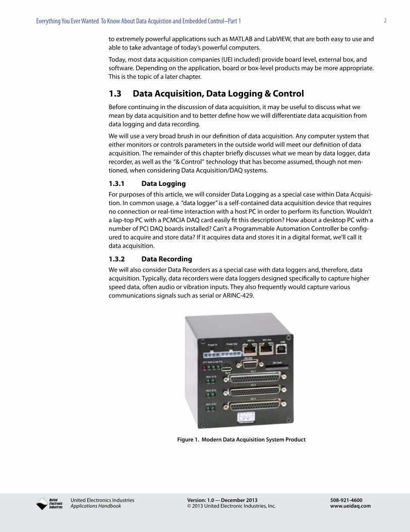
Figure 1. Modern Data Acquisition System Product

3Everything You Ever Wanted To Know About Data Acquistion and Embedded Control–Part 1
® United Electronics IndustriesApplications Handbook
Version: 1.0 — December 2013© 2013 United Electronic Industries, Inc.
508-921-4600www.ueidaq.com
1.3.3 “— & Control”Though not mentioned explicitly, data acquisition to most people involved in the industry has always meant data acquisition and control. There are a wide variety of vendors who consider themselves DAQ and though I have been in the industry for over 20 years, I am not aware of a single successful vendor that does (or did) not offer analog or digital output capability. Com-mon usage of “Data Acquisition / DAQ” implicitly implies the “& Control” part of the system.
1.4 Board- vs. Box-based SystemsPC-based DAQ systems are available with a wide variety of interfaces. Ethernet, PCI, USB, PXI, PCI Express, Firewire, Compact Flash and even the venerable GPIB, RS-232/485, and ISA bus are all popular. Which one(s) is/are the most appropriate for a given application may be far from obvious.
Perhaps the first question to address when considering a new DAQ project is whether the application is best served by a plug-in board system (e.g., UEI’s PD2 series of PCI boards) or an external “box” based system (e.g., UEI’s PowerDNA Cubes or various USB devices available from many vendors). This issue has been a source of much confusion (and competition) over the years, and the decision may be less well defined today than ever.
In the early days of PC-based DAQ, the rule of thumb was: High speed measurements were per-formed by board solutions, high accuracy was the domain of the external box. Of course, there was a “gray” area in between that could be addressed by either form factor.
Today’s gray area is much larger than ever before. Board level solutions offering 24-bit resolution are now available as are 6.5 digit DMM boards. On the box side, USB 2.0 is theoretically capable of delivering 30 million 16-bit conversions per second and Gigabit Ethernet will handle more than twice that. Though internal plug-in slot data transfer rates have increased 10 fold in recent years, the typical data acquisition system sample rate has not. Planes and cars don’t go much faster now than in 1980 and temperatures and pressures are still relatively slow changing phenomena.
Since most application accuracy and sample rates are perfectly within the capabilities of both board and box level solutions, other considerations will determine which solution is best for a given application. Some of these key factors as well as why they are key are listed below.
1.5 Tradeoffs and Considerations1.5.1 Distance from the PC to the Sensor or MeasurementThis is a more important consideration than many people realize and it’s important for two reasons. First, running long wires from your test system and sensors can be a very expensive proposition, especially in large systems. Running a single communication cable, on the other hand, is inexpensive. Also, each foot of wire connecting your sensor or output to a remote host computer increases your susceptibility to noise. Quiet measurements of 18-bits or greater are almost impossible to obtain using long connection wires. Mounting the DAQ system close to the signal source, however, reduces this noise potential.
1.5.2 PortabilitySome systems need to be portable. There are many small, external box devices that meet this need better than trying to drag a desktop or tower PC around. However, don’t overlook PXI when portability is a requirement. There are a variety of compact 4- and 6-slot chassis available.

4Everything You Ever Wanted To Know About Data Acquistion and Embedded Control–Part 1
® United Electronics IndustriesApplications Handbook
Version: 1.0 — December 2013© 2013 United Electronic Industries, Inc.
508-921-4600www.ueidaq.com
1.5.3 Number of I/O ChannelsMost people assume the external systems allow for more expandability and may be a better selection for a large system than a plug-in board system. That is often true and most of today’s desktop and tower PCs only include a few I/O slots. However, though considerably more ex-pensive than a standard desktop PC, there are a large variety of server and industrial computer chassis providing as many as 16 I/O slots. PXI chassis with up to 18 slots are also available.
1.5.4 PC ObsolescenceExternal box systems certainly have the edge here. Even if your next PC is functionally identical to your existing computer, do you really want to remove all your I/O boards and install them in your new computer? Also, as technology changes, the slots inside computers change. If your current system has 4 PCI boards in it, are you sure your next PC will have homes for them? Of course, there is no guarantee your next computer will have the same external connections as your current PC, but the probability is almost certainly higher.
1.5.5 Preferred Host ComputerIt’s no secret that laptop computers are becoming ever more popular and their capabilities have expanded to the point where they’re not just for road warriors any longer. Your options for developing a plug-in board-based DAQ system around your laptop are pretty limited. There are a variety of PCMCIA/PC-Card options available as well as a number of Compact Flash-based de-vices, but their capabilities and expandability are certainly limited. However, most new laptops come with Ethernet and USB ports, and many include Firewire as well.
1.5.6 PriceThe “old” rule of thumb was that all else being equal, a plug-in board based system was likely to carry a smaller price tag. This is no longer the case with some of the lowest cost DAQ interfaces ever released offering USB or Ethernet interfaces.
1.5.7 Pure SpeedThe internal buses will almost, by definition, be faster than those based upon an external com-munications link. After all, if the computer itself can’t keep up with the speed of an external communications port, the extra speed is unlikely to be useful. However, only the highest speed applications are beyond the capability of USB, Ethernet, or Firewire.
1.6 Popular PC InterfacesThe remainder of the chapter discusses the popular computer interfaces used in today’s DAQ products and briefly touches on the advantages and disadvantages of each.
1.6.1 Ethernet (100Base-T)Originally released in 1980, Ethernet has become the standard network of PCs worldwide. Oddly, it is only fairly recently that we have seen general acceptance of Ethernet as a computer interface in DAQ/Measurement systems. Theories abound explaining Ethernet’s slow migration into DAQ, perhaps the most common is that previously many engineers felt Ethernet systems were too difficult to configure and only trained IT personnel should dare. Of course, as the technology advanced, things got simpler, and today most teenagers are perfectly capable of installing a LAN in their houses and even most of us old-timers will have an easier time setting up a network than programming the VCR!
Standard Ethernet’s 100 Mbps data transfer rate is fast enough for all but the fastest DAQ ap-plications and its 100-meter range is also sufficient for the vast majority of systems. Ethernet sys-tems can also be quite portable, since the only tie required to the host computer is a CAT5 cable.

5Everything You Ever Wanted To Know About Data Acquistion and Embedded Control–Part 1
® United Electronics IndustriesApplications Handbook
Version: 1.0 — December 2013© 2013 United Electronic Industries, Inc.
508-921-4600www.ueidaq.com
Ethernet-based systems are easily expanded as ports may be added with extremely low cost, off the shelf routers. However, users should be careful to keep track of total system bandwidth requirements as all of the devices on a single Ethernet port share the bandwidth. Ethernet ports are included on virtually all computers sold these days and most evidence points to this continuing for the foreseeable future. The IEEE has worked very hard to maintain backward compatibility among Ethernet revisions and so even as the Ethernet specification progresses, Ethernet equipment purchased today should be useful for many years to come. Ethernet communication is generally considered very secure and is therefore used by some of the larg-est manufacturing and office facilities. Inter operability of Ethernet based DAQ devices from multiple vendors has not always been stellar. However, most Ethernet based DAQ (as opposed to Instrument) systems are single vendor and this has not been a major issue in the DAQ space. The LXI Consortium has developed a specification that ensures simple and seamless multi-vendor interoperability.
1.6.2 Gigabit Ethernet (1000Base-T)As the name implies, Gigabit Ethernet is a version of Ethernet that supports 1 Gigabit per second data transfer rates. Other Ethernet specifications, such as deployment range and data types, remain unchanged. One thing to note is that to take advantage of the Gigabit band-width, your system needs to be developed accordingly. This means using either Cat5e or Cat6 cables, as well as a adding a Gigabit port to your computer and Gigabit routers/switches.
Gigabit is still a new technology, so most Ethernet-based DAQ products do not yet support the faster band-width (and in many, if not most, applications, the extra bandwidth is not required). However, many new computers’ standard Ethernet interface/ports are now 1000Base-T capable and low cost, off-the-shelf Gigabit routers/switches are also available (e.g., I just saw a 5-port switch advertised for $29.99).Ultimately, most networks of the future will probably be devel-oped as Gigabit, but in most cases there may be little reason to retrofit existing networks or installations.
1.6.3 Fiber Ethernet (100Base-FX)Boasting the same speed capability as standard Ethernet, the fiber optic implementation ex-tends the range of the system to 2 kilometers (6,560 feet). Fiber interfaces are far from standard equipment on today’s PCs, but 100Base-T to 100Base-FX converters are readily available as are PCI plug-in boards with 100Base-FX interfaces. For applications requiring even larger distances, single mode fiber links extend the useful range up to 20 km (12.4 miles). Single mode fiber systems, however, come with a fairly high price tag.
In addition to their ability to extend control beyond standard Ethernet distances, the Fiber inter-faces have a number of other advantages. First, and probably foremost, is that they are almost immune to electrical and magnetic interference. If your application needs to communicate reliably in a noisy environment, therefore, fiber may be the way to go. Fiber also provides virtu-ally absolute electrical isolation. If there’s a good chance your DAQ system is going to take a big electrical hit and you want to make sure your host PC doesn’t get fried, look to fiber. Finally, from a security point of view, fiber doesn’t radiate any electrical or magnetic fields that can be “sniffed out” by uninvited guests.
1.6.4 Firewire (IEEE-1394a and b)Initially developed by Apple Computer (with support from others), Firewire is a high speed serial interface. The Firewire specification is maintained by the IEEE and is known as IEEE-1394. The original spec, released in 1995, supported 400 Mbps transfers and is also known as Firewire 400. In 2002, IEEE-1394b was released and supports data transfer rates up to 800 Mbps (a.k.a. Firewire 800). The “b” version also extends the maximum distance between devices. Though the distance extends beyond the original 4.5 meters, the maximum data transfer rate is reduced.

6Everything You Ever Wanted To Know About Data Acquistion and Embedded Control–Part 1
® United Electronics IndustriesApplications Handbook
Version: 1.0 — December 2013© 2013 United Electronic Industries, Inc.
508-921-4600www.ueidaq.com
The original target markets for Firewire were video and audio products. In these areas, Firewire has been very successful and has a significant market share. Firewire also has the basic require-ments to make it an excellent backbone for data acquisition systems. However, at approximate-ly the same time Firewire was being promoted, USB was coming on line. It appears that USB has “won” the battle for DAQ though the reasons are not intuitively obvious. At this time, there are a wide variety of DAQ vendors and products actively promoting USB devices, while with a few ex-ceptions, Firewire success has been confined to the original target market of Audio and Video.
1.6.5 GPIB (IEEE-488)Originally developed by HP and designated HPIB, the GPIB bus remains the dominant intercon-nection standard between computers and instruments though Ethernet and USB are begin-ning to make inroads. However, as prevalent as GPIB is in T&M applications, it has never had a substantial impact on the data acquisition market. There are a number of GPIB DAQ products available, but their market penetration is very small relative to PCI, PXI, Ethernet, and USB based products.
1.6.6 PCI (Peripheral Component Interconnect) BusThe PCI bus is arguably the most common DAQ interface used today. Though Ethernet, USB, and PXI are all significant and growing, and PCI Express is “looking for a fight”, PCI is still the workhorse. It is very fast relative to almost all of the external box interconnection systems. PCI slots (of some sort) are also included in virtually all desktop and tower PCs.
PCI was originally developed by Intel as an interface to connect various functions on mother-boards. It wasn’t long before it was generalized as a replacement for the aging 16-bit ISA bus that had dominated early PCs. With its “blazing” 33 MHz clock rate, a full 32-bit data path and Windows 95’s excellent support (including plug and play) it wasn’t long before the PCI bus had totally eclipsed the ISA bus in new “consumer” computers.NOTE: Though you’d be unlikely to ever find a new computer from one of the major consumer suppliers with an ISA slot, the ISA bus market is surprisingly vibrant. ISA DAQ boards installed in industrial computers are still the backbone of many systems!
Though PCI has remained the industry standard since the middle 90’s, it has not remained stagnant. The PCI “standard” has moved from 33 MHz to 66 MHz. It also grew from a 32-bit bus to 64-bits. Also, as the industry moved from +5 VDC to +3.3 VDC logic, the specification was re-vised so as to support both. Throughout all of this, the spec has done a remarkably good job of maintaining backward compatibility. Cards designed in the mid 90s may still be used in many PCs purchased today.
The original PCI 33 MHz, 32-bit spec provided maximum transfer rates of 133 Megabytes per second. This was (and remains) fast enough for all but the highest speed data acquisition ap-plications. Most DAQ boards today only take advantage of 32-bit transfers and support both 3.3 and 5 VDC interfaces. A new version of the PCI spec eliminates +5V support, but it is not yet known if this spec will become a common standard or will be eclipsed by other technology (e.g., PCI Express).
1.6.7 PCI ExpressThe latest of the computer interfaces to become common on standard computers, PCI Express is the first “all new” plug-in, general purpose computer bus to become popular since PCI. PCI Express slots are now found in most new desktop and tower PCs.
PCI Express abandoned the parallel data transfer architecture of PCI and PCI-X. Instead, PCI-Express is based upon multiple very high speed (~2 Gbps) serial paths. The serial nature of PCI Express becomes evident when you look at a PCI Express board and notice how small the board’s PC interface is and how few “golden fingers” the boards have. Though 2 Gbps is quite fast, the PCI Express spec is not done there. PCI Express allows up to 16 of these serial links in

7Everything You Ever Wanted To Know About Data Acquistion and Embedded Control–Part 1
® United Electronics IndustriesApplications Handbook
Version: 1.0 — December 2013© 2013 United Electronic Industries, Inc.
508-921-4600www.ueidaq.com
each direction. The total possible data transfer rate of a full PCI Express implementation is 32 Gbps in each direction.
It is too early to determine the ultimate impact of PCI Express on the DAQ market. There are a variety of DAQ boards supporting PCI Express at this time, but only time will tell whether it, or some alternative, becomes the next de facto plug-in board standard.
1.6.8 PCI-XPCI-X (sometimes confused with PCI Express) is a recent variant on the 64-bit PCI specification. The original PCI-X spec bumped the bus clock speed to 100 MHz and then 133 MHz. A new version of the specification bumps the clock rate to as high as 533 MHz. Even the most recent specification maintains backward compatibility with slower PCI boards, but of course the legacy boards cannot take advantage of the higher speeds. PCI-X has never become a signifi-cant factor in the DAQ market, though there may be a number of PCI-X DAQ boards available.
1.6.9 PXIThe PXI bus is electrically identical to PCI. PXI chassis, however, are developed specifically with measurement/DAQ applications in mind. All boards (including the CPU module) plug into the front of a PXI chassis. This allows much easier installation as no PC cover need be removed.
Also, the connectors of the boards plugged in are at the front of the chassis, which makes them much easier to get to in most applications.
The PXI specification covers much more than simply the computer interface and mechanical structure. The PXI backplane also offers a number of powerful triggering capabilities and man-dates various “good neighbor” requirements so that boards from multiple vendors may all be easily integrated.
If there is a downside to the PXI market, it’s that the CPU modules are specific to the PXI form factor. PXI CPUs don’t take advantage of the huge economies of scale the consumer PC makers have, so a PXI CPU is likely to cost much more than a computer with equivalent horsepower from a company like Dell, Gateway, or HP. Of course, in many applications, the convenience of the PXI form factor more than makes up for the added cost. It should be noted that it is possible to control a PXI chassis from an independent host PC by installing a special “gateway” module in slot 0. Though this does allow an off the shelf, COTS computer to serve as a PXI controller, the Gateway interface systems are typically more expensive than the host computer and the price advantage of going to a COTS host are lost.
PXI has been very well received by the market and PXI products are available from a very large number of vendors. The specification is controlled by the PXI Systems Alliance. For more details about PXI, please see http://www.pxisa.org.
1.6.10 PXI ExpressPXI Express is an implementation of PCI express. There are a variety of PXI Express products available, though as a very new specification, it is difficult to predict the ultimate acceptance of PXI Express products.
1.6.11 RS-232People have been writing eulogies for the venerable RS-232 since I was a young engineer in the early 80s. However, the last survey result I saw indicated it was still the single most common interface between a PC and an external DAQ device. RS-232 is slow, fairly subject to noise and fairly short range, yet it remains ubiquitous. However, for the first time, new PCs have replaced the once common RS-232 port with USB ports and most external “consumer” devices have abandoned the RS-232. Could this finally be the end of RS-232? Time will tell.
8Everything You Ever Wanted To Know About Data Acquistion and Embedded Control–Part 1
® United Electronics IndustriesApplications Handbook
Version: 1.0 — December 2013© 2013 United Electronic Industries, Inc.
508-921-4600www.ueidaq.com
1.6.12 RS-422/485RS-422 and its networkable sibling, RS-485, has also been around a long time. Though slow by most standards, it is fast enough for many applications and has an excellent 1200-meter range. RS-485 has been especially well accepted by manufacturers (and buyers) of slow, low channel count, remote DAQ modules.
1.6.13 USBUSB has totally supplanted RS-232 as the communications interface of choice for most consumer items such as printers, cameras and the like. Though the initial releases (v1.0 and 1.1) were slow for a number of applications, version 2.0 has all the bandwidth most DAQ applications will ever require. Virtually every new computer includes multiple USB ports. It has also become very pop-ular in the DAQ marketplace and there are a large number of vendors offering USB-based DAQ.
USB’s simple plug-and-play installation, combined with its 480 Mbps data transfer rate, make it an ideal interface for many data acquisition applications. Also, the popularity of USB in the con-sumer market has made USB components very inexpensive. New, low cost, USB DAQ devices are now available at previously unheard-of prices
USB’s 5-meter range is perhaps its largest detraction as it limits the ability to implement remote and distributed I/O systems based on USB. There is also concern among some in the industrial arena that the USB connection’s lack of a locking cable mechanism might allow a USB cable to vibrate out of its connector. Whether this is a real possibility or not is certainly open to debate.
1.6.14 WirelessAn entire article could be written on the various options of wireless technologies and how they could apply to DAQ. However, the reality of the market as it stands right now is that the dedi-cated wireless-based DAQ market is still very small. There are a number of vendors who now offer wireless DAQ interfaces based upon such standards as Zigbee and 802.15.4 and variants of the 802.11 standard. There are also a growing number of customers implementing systems based on standard copper Ethernet devices, such as UEI’s PowerDNA Cube. Rather than using CAT-5 connections between the host PC and the DAQ device, however, they are opting to use standard off-the-shelf wireless routers from firms like Linksys and Netgear.
The next chapter starts the discussion of data acquisition I/O, and in particular, the all impor-tant analog input. Subsequent chapters will discuss other I/O types such as analog output, digital I/O, and counter/timer.
1.7 Analog InputsThe analog input is the backbone of the data acquisition market. Though other I/O types play key roles in many applications, the vast majority of DAQ systems include analog input and a good percentage of them require only analog input.
We will define analog input by exclusion. Any input that is not digital, that is not defined as two states, (e.g., high/low or one/zero) will be considered analog. Common analog inputs include such measurements as temperature, pressure, flow, strain as well as the direct measurement of voltage and current.
Analog inputs are “measured” by a device called an A/D (Analog to Digital) converter (some-times also referred to as an ADC). Though we’ll discuss A/D converter technology in the next section, it may be useful to mention here that A/D and analog input are often used inter-changeably when referring to a DAQ product. In common usage, an analog input board and A/D board are the same thing. Similarly, an analog input channel and an A/D channel perform the same function.

9Everything You Ever Wanted To Know About Data Acquistion and Embedded Control–Part 1
® United Electronics IndustriesApplications Handbook
Version: 1.0 — December 2013© 2013 United Electronic Industries, Inc.
508-921-4600www.ueidaq.com
1.8 A/D ConvertersAn A/D converter does exactly what its name implies. It is connected to an analog input signal, it measures the analog input and then provides the measurement in digital form suitable for use by a computer. The A/D converter is the heart of any analog input DAQ system as it is the device that actually performs the measurement of the signal.
1.8.1 ResolutionThe resolution of an A/D input channel describes the number or range of different possible measurements the system is capable of providing. This specification is almost universally provided in term of “bits”, where the resolution is defined as: 2 (# of bits)—1. For example, 8-bit resolution corresponds to a resolution of one part in 28—1 or 255. For resolutions above 12-bit, the “- 1” term becomes virtually insignificant and it is dropped. A resolution of 16-bits corre-sponds to one part in 216 or 65,536. The minimum difference in a measurement is one bit. This one bit is frequently referred to as the Least Significant Bit or LSB.
When combined with an input range, the resolution determines how small a change in the input is detect-able. To determine the resolution in engineering units, simply divide the range of the input by the resolution.
A 16-bit input with a 0-10 Volt input range provides 10 V / 216 or 152.6 microvolts. Table 1 pro-vides a comparison of the resolutions for the most commonly used converters in DAQ systems.
Table 1. Common ADC Converter Resolutions
8-bit 12-bit 16-bit 18-bit 24-bit
Distinct Levels 256 4,096 65,536 262,144 16,777,216
Resolution, ±10 V scale 78.4 mV 4.88 mV 305 µV 76.4 µV 1.192 µV
Resolution in °C, K type TC, ±0.5 Volt Full Scale input range (~25 °C) 97.7 6.10 0.38 0.10 0.00149
Dynamic Range in dB 48.2 72.2 96.3 108.4 144.5
Table 1 shows the resolutions of the more commonly used A/D converters in levels as well as in a number of common engineering units.
In general, the higher the A/D converter’s resolution, the more accurate it will be. However, a DAQ device’s overall measurement accuracy relies on much more than the accuracy of the A/D converter. A high resolution product is not always an accurate product. For example, many au-dio input products offer 24-bit resolution, but offer only 1% (about 7-bit) overall accuracy. This lack of accuracy is typically fine for an audio measurement, but could be unworkable in a strain measurement. Overall system accuracy concerns will be left to a subsequent section while this section returns its focus back to A/D converters.
1.8.2 A/D Converter TypesThere are a variety of different types of A/D converters used in data acquisition. A detailed description of A/D converters could take an entire book and is beyond the scope of this note. However, a cursory knowledge of the different types of converters and, in particular, their rela-tive strengths and weaknesses should prove beneficial. The most commonly used A/D con-verters in today’s DAQ products are the: Successive Approximation, Delta Sigma (a.k.a. Sigma Delta), Flash, and Dual Slope/Integrating. The text below describes the various converter types while an overview of each type’s key parameters is depicted in Table 1.

10Everything You Ever Wanted To Know About Data Acquistion and Embedded Control–Part 1
® United Electronics IndustriesApplications Handbook
Version: 1.0 — December 2013© 2013 United Electronic Industries, Inc.
508-921-4600www.ueidaq.com
1.8.3 Successive Approximation (SA)These converters remain the backbone of the DAQ industry. They typically provide resolutions in the 10 to 18-bit range, and depending on the resolution, offer sample rates up to tens of Megasamples per second. The basic underlying technology of SA involves comparing the input to the output of an on-chip D/A converter. Based upon whether the D/A converter output is higher or lower than the input, the D/A converter output is raised or lowered. In this manner, the SA converter ultimately zeroes in and when the D/A converter output is equal to the input (within one LSB), the iteration ends and the current digital word is written to the A/D output. The majority of UEI “Cube” I/O layers and all of UEI’s PCI/PXI analog input boards use successive approximation converter technology.
1.8.4 Sigma Delta (also known as Delta Sigma)Some manufacturers refer to this type of converter as delta sigma, while others call it a sigma delta. Sigma Delta appears to be the more popular designation at this time. Regardless of the “chicken or the egg” nature of what the converters are called, the sigma delta converter is rapidly becoming the standard by which other converters are judged and is seen in more and more DAQ devices each day. Perhaps the most differentiating feature of sigma delta converters is that they provide resolution up to 24-bits. Another interesting feature of converters is that they inherently trade off sample rate with resolution. Many converters provide an ability to sample at high speeds at low(er) resolutions or to slow down and sample at a rate that provides the maximum possible resolution.
Without going too much into the technology, the concept is fairly simple. A lower resolution converter inside the converter (typically 1-bit) is dramatically oversampled, i.e., sampled faster (in this case, orders of magnitude faster) than the sample rate your DAQ system desires. The large number of “one-bit” A/D con-versions is then digitally integrated. The resolution is deter-mined by the number of “internal” samples taken. A high number of internal samples provides a higher resolution with a lower overall converter sample rate. If you sample fewer times, you receive your A/D converter data faster, but at lower resolution. The converters are not without their share of design issues, but these are being addressed by the various manufacturers at a high rate and they will almost certainly supplant the Successive Approximation converter in the reason-ably near future. A number of UEI analog input boards take advantage of converter technology, including the 25-channel, 24-bit resolution DNA-AI-225.
1.8.5 FlashFlash converters can be extremely fast, though they do not typically offer high resolution. Sample rates in the gigahertz range are possible, but flash converters are rarely seen with resolutions greater than 8 bits. A flash converter is really nothing more than a string of com-parators with highly trimmed input resistors. One side of each comparator input is set at one bit of resolution greater than the next. That means any given input to the A/D converter will always fall between the reference inputs of two adjacent comparators, driving one comparator output high, with the adjacent output low. This data is then taken into a decoder, and the posi-tion where the switch from 0 to 1 occurs defines the A/D output. As mentioned previously, it is a simple concept, but as a Flash converter requires at 2n comparators, the amount of circuitry required on the chip gets huge as the converter resolution increases. An 8-bit flash converter requires 255 comparators. That’s a lot of analog circuitry on a single chip, even at today’s densi-ties. Try to add one bit of resolution and you push the total number of comparators required to 511. A very difficult challenge indeed.
1.8.6 Dual Slope / IntegratingOnce the king of the high resolution A/D converter market, dual slope converters are seldom seen in new designs. As with the flash converter, the longer you are willing to wait for your
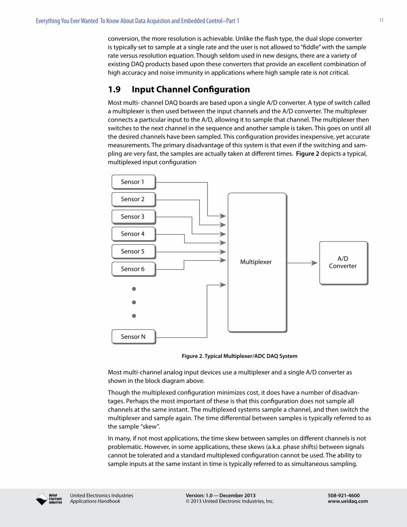
11Everything You Ever Wanted To Know About Data Acquistion and Embedded Control–Part 1
® United Electronics IndustriesApplications Handbook
Version: 1.0 — December 2013© 2013 United Electronic Industries, Inc.
508-921-4600www.ueidaq.com
conversion, the more resolution is achievable. Unlike the flash type, the dual slope converter is typically set to sample at a single rate and the user is not allowed to “fiddle” with the sample rate versus resolution equation. Though seldom used in new designs, there are a variety of existing DAQ products based upon these converters that provide an excellent combination of high accuracy and noise immunity in applications where high sample rate is not critical.
1.9 Input Channel ConfigurationMost multi- channel DAQ boards are based upon a single A/D converter. A type of switch called a multiplexer is then used between the input channels and the A/D converter. The multiplexer connects a particular input to the A/D, allowing it to sample that channel. The multiplexer then switches to the next channel in the sequence and another sample is taken. This goes on until all the desired channels have been sampled. This configuration provides inexpensive, yet accurate measurements. The primary disadvantage of this system is that even if the switching and sam-pling are very fast, the samples are actually taken at different times. Figure 2 depicts a typical, multiplexed input configuration
Sensor 1
Sensor 2
Sensor 3
Sensor 4
Sensor 5
Sensor 6
Sensor N
A/DConverter
Multiplexer
Figure 2. Typical Multiplexer/ADC DAQ System
Most multi-channel analog input devices use a multiplexer and a single A/D converter as shown in the block diagram above.
Though the multiplexed configuration minimizes cost, it does have a number of disadvan-tages. Perhaps the most important of these is that this configuration does not sample all channels at the same instant. The multiplexed systems sample a channel, and then switch the multiplexer and sample again. The time differential between samples is typically referred to as the sample “skew”.
In many, if not most applications, the time skew between samples on different channels is not problematic. However, in some applications, these skews (a.k.a. phase shifts) between signals cannot be tolerated and a standard multiplexed configuration cannot be used. The ability to sample inputs at the same instant in time is typically referred to as simultaneous sampling.
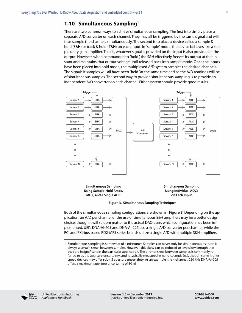
12Everything You Ever Wanted To Know About Data Acquistion and Embedded Control–Part 1
® United Electronics IndustriesApplications Handbook
Version: 1.0 — December 2013© 2013 United Electronic Industries, Inc.
508-921-4600www.ueidaq.com
1.10 Simultaneous Sampling1
There are two common ways to achieve simultaneous sampling. The first is to simply place a separate A/D converter on each channel. They may all be triggered by the same signal and will thus sample the channels simultaneously. The second is to place a device called a sample & hold (S&H) or track & hold (T&H) on each input. In “sample” mode, the device behaves like a sim-ple unity gain amplifier. That is, whatever signal is provided on the input is also provided at the output. However, when commanded to “hold”, the S&H effectively freezes its output at that in-stant and maintains that output voltage until released back into sample mode. Once the inputs have been placed into hold mode, the multiplexed A/D system samples the desired channels. The signals it samples will all have been “held” at the same time and so the A/D readings will be of simultaneous samples. The second way to provide simultaneous sampling is to provide an independent A/D converter on each channel. Either system should provide good results.
Sensor 1
Sensor 2
Sensor 3
Sensor 4
Sensor 5
Sensor 6
Sensor N
SHA
SHA
SHA
SHA
SHA
SHA
SHA
A/DConverter
MUX
Trigger
Sensor 1
Sensor 2
Sensor 3
Sensor 4
Sensor 5
Sensor 6
Sensor N
ADC
ADC
ADC
ADC
ADC
ADC
ADC
Logic
Trigger
Simultaneous Sampling Using Sample-Hold Amps,
MUX, and a Single ADC
Simultaneous Sampling Using Individual ADCs
on Each Input
Figure 3. Simultaneous Sampling Techniques
Both of the simultaneous sampling configurations are shown in Figure 3. Depending on the ap-plication, an A/D per channel or the use of simultaneous S&H amplifiers may be a better design choice, though it will seldom matter to the actual DAQ users which configuration has been im-plemented. UEI’s DNA-AI-205 and DNA-AI-225 use a single A/D converter per channel, while the PCI and PXI-bus based PD2-MFS series boards utilize a single A/D with multiple S&H amplifiers.
1 Simultaneous sampling is somewhat of a misnomer. Samples can never truly be simultaneous as there is always a certain skew between samples. However, this skew can be reduced to levels low enough that they are insignificant in the particular application. The error or skew between samples is commonly re-ferred to as the aperture uncertainty, and is typically measured in nano-seconds (ns), though some higher speed devices may offer sub-nS aperture uncertainty. As an example, the 4-channel, 250 kHz DNA-AI-205 offers a maximum aperture uncertainty of 30 nS
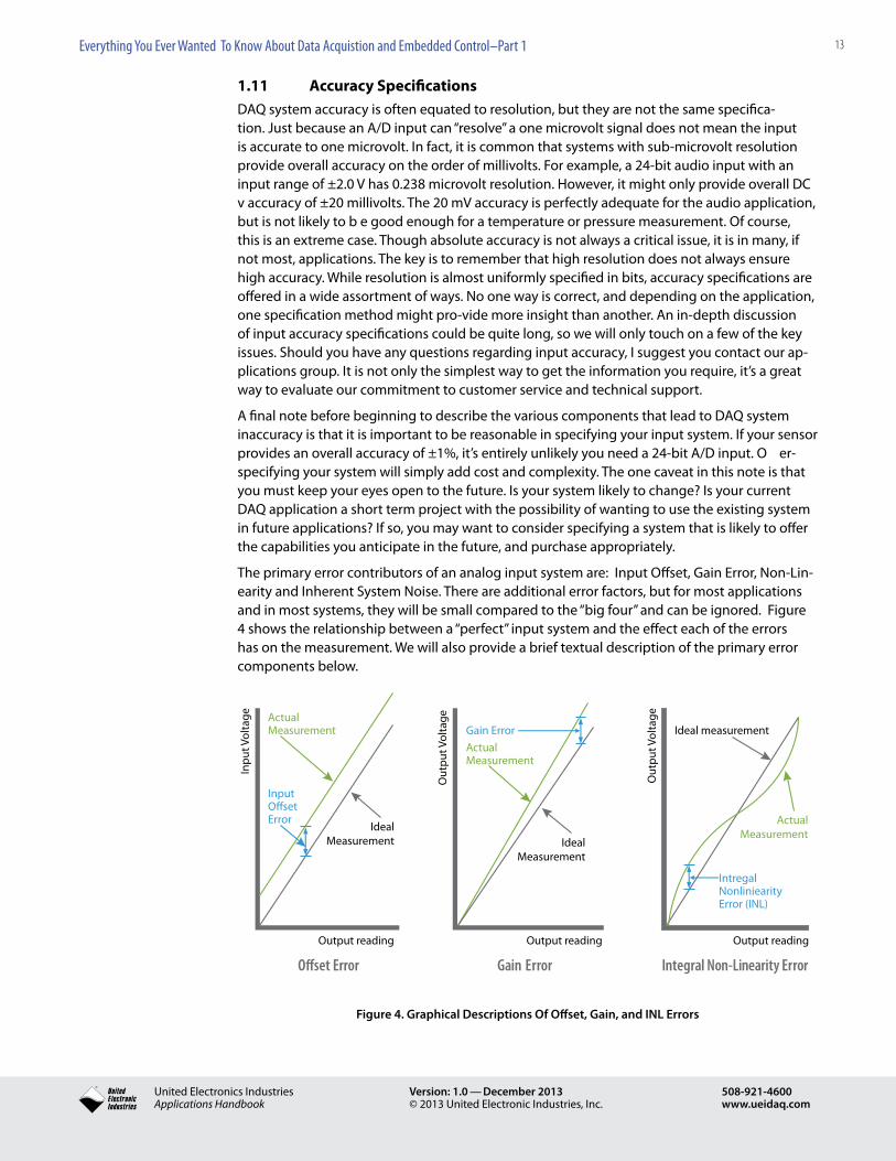
13Everything You Ever Wanted To Know About Data Acquistion and Embedded Control–Part 1
® United Electronics IndustriesApplications Handbook
Version: 1.0 — December 2013© 2013 United Electronic Industries, Inc.
508-921-4600www.ueidaq.com
1.11 Accuracy SpecificationsDAQ system accuracy is often equated to resolution, but they are not the same specifica-tion. Just because an A/D input can “resolve” a one microvolt signal does not mean the input is accurate to one microvolt. In fact, it is common that systems with sub-microvolt resolution provide overall accuracy on the order of millivolts. For example, a 24-bit audio input with an input range of ±2.0 V has 0.238 microvolt resolution. However, it might only provide overall DC v accuracy of ±20 millivolts. The 20 mV accuracy is perfectly adequate for the audio application, but is not likely to b e good enough for a temperature or pressure measurement. Of course, this is an extreme case. Though absolute accuracy is not always a critical issue, it is in many, if not most, applications. The key is to remember that high resolution does not always ensure high accuracy. While resolution is almost uniformly specified in bits, accuracy specifications are offered in a wide assortment of ways. No one way is correct, and depending on the application, one specification method might pro-vide more insight than another. An in-depth discussion of input accuracy specifications could be quite long, so we will only touch on a few of the key issues. Should you have any questions regarding input accuracy, I suggest you contact our ap-plications group. It is not only the simplest way to get the information you require, it’s a great way to evaluate our commitment to customer service and technical support.
A final note before beginning to describe the various components that lead to DAQ system inaccuracy is that it is important to be reasonable in specifying your input system. If your sensor provides an overall accuracy of ±1%, it’s entirely unlikely you need a 24-bit A/D input. O er-specifying your system will simply add cost and complexity. The one caveat in this note is that you must keep your eyes open to the future. Is your system likely to change? Is your current DAQ application a short term project with the possibility of wanting to use the existing system in future applications? If so, you may want to consider specifying a system that is likely to offer the capabilities you anticipate in the future, and purchase appropriately.
The primary error contributors of an analog input system are: Input Offset, Gain Error, Non-Lin-earity and Inherent System Noise. There are additional error factors, but for most applications and in most systems, they will be small compared to the “big four” and can be ignored. Figure 4 shows the relationship between a “perfect” input system and the effect each of the errors has on the measurement. We will also provide a brief textual description of the primary error components below.
Figure 4. Graphical Descriptions Of Offset, Gain, and INL Errors
InputOffsetError
Inp
ut V
olta
ge
Output reading Output reading Output reading
Out
put
Vol
tage
Out
put
Vol
tage
Ideal measurementGain Error
IdealMeasurement
Offset Error Gain Error Integral Non-Linearity Error
ActualMeasurement
ActualMeasurement
IdealMeasurement
IntregalNonliniearityError (INL)
ActualMeasurement
14Everything You Ever Wanted To Know About Data Acquistion and Embedded Control–Part 1
® United Electronics IndustriesApplications Handbook
Version: 1.0 — December 2013© 2013 United Electronic Industries, Inc.
508-921-4600www.ueidaq.com
1.11.1 Input OffsetAssuming all other errors are zero, input offset is a constant difference between the meas-ured input and the actual input voltage. For example, if the input offset voltage was +0.1 volt, measurements of perfect 1, 2 and 5-volt input signals would provide readings of 1.1, 2.1 and 5.1 volts, respectively. In a real system, the other errors are never zero, which complicates the measurement of input offset. Most analog input specifications define the input offset as the measurement error at 0 volts.
Note that some DAQ products, such as the DNA-AI-207, provide an “auto zeroing” capability. This function drives the input offset error to zero, or at least to a level low enough that its con-tribution is no longer significant relative to other errors.
The UEI DNA-AI-207 provides an auto-zero capability that reduces the input offset error to an insignificant level relative to the board’s 18-bit resolution, resulting in the “ideal” measurement curve shown in Figure 4.
1.11.2 Gain ErrorIt is easiest to illustrate this error by first assuming all other errors are zero. Gain error is the difference in the slope (in volts per bit) between the actual system and an ideal system. For example, if the gain error is 1%, the gain error at 1 volt would be 10 millivolts (1 * .01), while the error at 10 volts would be ten times as large at 100 millivolts.
In a real world system where the other errors are not zero, the gain error is usually defined as the error of the measurement as a percentage of the full scale reading. For example, in our 0—10 volt example range, if the error at 10 V (or more often at a reading arbitrarily close to 10 volts such as 9.99 V) is 1 millivolt, the gain error specified would be 100*(.001 / 10) or .01%. For higher precision measurement systems, the gain error is often specified in parts per million (or ppm) rather than percent as it’s a bit easier to read. To calculate the error in parts per mil-lion, simply multiply the input error divided by the input range by one million. In our example above, the 0.01% would be equivalent to 1,000,000 * .001 / 10 or 100 ppm.
Though many products offer auto-calibration, which substantially reduces the gain error, it is not possible to eliminate it completely. The automated gain calibration is almost always per-formed relative to an internally supplied reference voltage. The reference voltage will drift over time and any error in the reference will trans-late into a gain error. It is possible to create refer-ences with arbitrarily small errors. However, as the gain error gets small relative to other system errors, it becomes economically unfeasible to improve the reference accuracy. In addition to the cost penalty involved in providing the “pseudo perfect” reference, one of the errors, if not the largest, in most references is the drift with temperature. The only way to eliminate this drift is to maintain the reference temperature at a constant level. This is not only expensive, but it also requires a significant amount of power, which increases overall system power consumption
1.11.3 Non-LinearityAs its name implies, non-linearity is the difference between the graph of the input measurement versus actual voltage and the straight line of an ideal measurement. The non-linearity error is composed of two components, integral non-linearity (INL) and differential non linearity (DNL).
Of the two, integral non-linearity is typically the specification of importance in most DAQ systems. The INL specification is commonly provided in “bits” and describes the maximum er-ror contribution due to the deviation of the voltage versus reading curve from a straight line. Though a somewhat difficult concept to describe textually, INL is easily described graphically and is depicted in Figure 4. Depending on the type of A/D converter used, the INL specification can range from less than 1 LSB to many, or even tens, of LSBs.
15Everything You Ever Wanted To Know About Data Acquistion and Embedded Control–Part 1
® United Electronics IndustriesApplications Handbook
Version: 1.0 — December 2013© 2013 United Electronic Industries, Inc.
508-921-4600www.ueidaq.com
Differential non-linearity describes the “jitter” between the input voltage differential required for the A/D converter to increase (or decrease) by one bit. The output of an ideal A/D converter will increment (or decrement) one LSB each time the input voltage increases (or decreases) by an amount exactly equal to the system resolution. For example, in a 24-bit system with a 10-volt input range, the resolution per bit is 0.596 microvolt. Real A/D converters, however, are not ideal and the voltage change required to increase or decrease the digital output varies.
DNL is typically ±1 LSB or less. A DNL specification greater than ±1 LSB indicates it is possible for there to be “missing” codes. Though not as problematic as a non-monotonic D/A converter, A/D missing codes do compromise measurement accuracy.
1.11.4 NoiseNoise is an ever-present error in all DAQ systems. Much of the noise in most systems is gener-ated externally to the DAQ system and “picked-up” in the cabling and field wiring. However, every DAQ system has inherent noise as well. This noise is commonly measured by shorting the inputs at the board or device connector and acquiring a series of samples. An ideal system response would be a constant zero reading. In almost all systems, however, the reading will bounce around over a number of readings1. The magnitude of the “bounce” is the inherent noise. The noise specification can be provided in either bits or volts, and as peak-to-peak or Root Mean Square (RMS).
The key consideration with noise is to factor it into the overall error calculations. Note that a 16-bit input system with 3 bits RMS of noise is not going to provide much better than 13-bit accuracy. The three least significant bits will be dominated by noise and will contain very little useful information unless many samples are taken and the noise is averaged out.
1.11.5 Calculate the Total ErrorTo determine overall system error, simply add the offset, linearity, gain, and noise errors to-gether. Though it can be argued that it is unlikely all three of the offset, linearity and gain errors will contribute in the same direction, it is certainly risky to assume they will not. It is seldom prudent to ignore Murphy’s law!
Max Error = Input Offset + Gain Error + Non-Linearity Error + Noise
A final note is that in most systems, Input Offset, Gain Error, and Non-Linearity all vary over time, and in particular, over temperature. If you require a very accurate measurement and your DAQ system will be subject to extreme temperature fluctuations, be sure to consider the errors caused by temperature change in your calculations.
1.12 Sample Rate1.12.1 How fast is fast enough?“How quickly must I sample my input signal?” is a fairly common question among DAQ system designers, and especially those without formal training in either DAQ systems or sample theory. The simple answer is the system must sample fast enough to “see” the required changes in in-put. In a purely input system, the minimum required sample rate is typically defined by Nyquist sampling theory. Nyquist found that to recreate a waveform, you need to sample at least twice as fast as the highest frequency component contained in the waveform. For example, if your input signal contains frequency components up to 1 kHz, you will want to sample at least at 2 kHz, and more realistically, at 2.5 – 3 kHz.
As with input resolution and accuracy, there is a tendency among DAQ system designers, particularly those new to the industry, to “over-specify” the system input sample rate. There are
1 If the average of the readings is not zero, it indicates the system has an input offset error.

16Everything You Ever Wanted To Know About Data Acquistion and Embedded Control–Part 1
® United Electronics IndustriesApplications Handbook
Version: 1.0 — December 2013© 2013 United Electronic Industries, Inc.
508-921-4600www.ueidaq.com
very few applications where it is necessary to sample a thermocouple more than 10 times a sec-ond, and most will probably be adequately served at a tenth that rate. Avoid the temptation to over-sample as it often increases system cost, memory requirements, and subsequent analysis costs without adding any useful information
Note that the above pertains mostly to input-only systems. Control systems represent an entirely different set of considerations. Not only must the input sampling rate be high enough, but the CPU must have the “horsepower” to perform the calculations fast enough to keep the system stable and the output devices must have the speed and accuracy required to achieve the desired control results. A discussion of control theory is well beyond the scope of this note, but there we will add a few notes that may be helpful.
First, if you need any sort of deterministic control, and/or a hiccup in your control algorithm would be problematic, or your system update rate is more than 10 updates per second1, you will likely need to consider using a real-time or “pseudo real-time” operating system. UEI offers support for QNX, RT Linux, RTAI Linux, RTX and XPC. Many users also find that though it is not a fully deterministic real-time OS, Linux-based applications have low enough latencies to be used in some higher speed control applications.
1.13 DAQ “System” ConsiderationsBe careful to examine the analog input systems you are considering to determine if the sample rate specification provided is for each channel or for the entire board. As discussed previously, most DAQ input boards use a multi-channel multiplexer connected to a single A/D converter. Most “product” descriptions (e.g., 100 kilosample/second, 8-channel, A/D board), specify the total sample rate of the board or device. This allows sampling of one channel at 100 kS/s, but if more channels are required, the 100 kS/s is shared among all channels. For example, if two channels are sampled, each may only be sampled at 50 kS/s each. Similarly, 5 channels could be sampled at 20 kS/s each. If the specification does not specify the sample rate as “per-channel”, it is likely the sample rate must be divided among all channels sampled.
Another sample rate factor should be considered when various input signals contain widely varying frequency content. For example, an automotive test system may need to monitor vibra-tion at 20 kS/s and temperature at 1 S/s. If the analog input only samples at a single rate, the system will be forced to sample temperature at 20 kS/s and will waste a great deal of memory/disk space with the 19,999 temperature S/s that aren’t needed. Some systems, including all of UEI’s “Cube” based products, allow inputs to be sampled at different rates, while products from many vendors do not.
1 To ensure 10 updates/second in most Windows/Vista environments, you would also need to disable many automated functions such as Windows Update or Automated backups.
17Everything You Ever Wanted To Know About Data Acquistion and Embedded Control–Part 1
® United Electronics IndustriesApplications Handbook
Version: 1.0 — December 2013© 2013 United Electronic Industries, Inc.
508-921-4600www.ueidaq.com
6 I/O boards, each running at a different scan rate
Figure 5. UEI Cube with 6 I/O Boards
The final sampling rate concern is the need to sample fast enough, or provide filtering to prevent aliasing. If signals included in the input signal contain frequencies higher than the sample rate, there is the risk of aliasing errors. Without going into the mathematics of aliasing, we will just say that these higher frequency signals can and will manifest themselves as a low frequency error. Figure 6 provides a graphical representation of the aliasing phenomenon. A real life example of aliasing is common in movies. The blades of a helicopter/airplane or the spokes of a wheel appearing to be moving slowly and/or backwards is an example of aliasing. In the movies it doesn’t matter, but if the same phenomenon appears in the measured input signal, it’s a pure and sometimes critical error.
Sampled PointReconstructed Signal
Mag
nitu
de
Original Signal
Mag
nitu
de
Original Signal
Under Sampling
Time
Figure 6. Aliasing
As shown in Figure 6, aliasing is possible when the sampling rate is too slow. The problem may be corrected by sampling faster, or by inserting an anti-aliasing low-pass filter, which removes any undesirable higher frequency signals.
18Everything You Ever Wanted To Know About Data Acquistion and Embedded Control–Part 1
® United Electronics IndustriesApplications Handbook
Version: 1.0 — December 2013© 2013 United Electronic Industries, Inc.
508-921-4600www.ueidaq.com
There are really two solutions for aliasing. The first, and often simplest, is to sample at a rate higher than the highest frequency component in the signal measured. Some measurement purists will say that you can never be sure what the highest frequency in a signal will be, but in reality many, if not most, systems designers have very good a priori knowledge of the frequencies included in a given input signal. People do not use anti-aliasing filters on thermo-couples because they are almost never needed. With a good idea of the basics of the signals measured, it is usually a straightforward decision to determine if aliasing might or might not be a problem.
In some applications, such as audio and vibration analysis, aliasing is a very real concern and it is difficult to guarantee that a sample rate is faster than every frequency component in the waveform. These applications require an anti-aliasing filter. These filters are typically 4-pole or greater filters set at one half the sample rate. They prevent the higher frequency signals from getting to the system A/D converter, where they can create aliasing errors.
1.14 Input RangeThough a fairly obvious specification, Input Range is not one to ignore. If you have a ±15 volt signal, you’re not going to be happy with the results from a DAQ board with a fixed ±5 volt input range. Many systems these days have software programmable input ranges, though some still provide fixed input ranges. Either way, the signal measured should be smaller than the maximum input range of the DAQ input device.
Other than the obvious matching of the input range to your signal issue, one other input range consideration is whether the DAQ device is capable of setting different channels at different ranges. A single input range system measuring diverse signals (e.g. a thermocouple and a ±10 volt input) will require the system be set at a gain low enough to cover the largest input’s full scale range. This in effect reduces the resolution avail-able on signals with smaller full scale input ranges.
1.15 Differential and Single-ended InputsA differential input measures the voltage difference between two input terminals, while a single ended input measures the difference between and input and the DAQ device’s ground. The two different configurations are shown in Figure 7. Many data acquisition products have the ability to be configured as either differential or single-ended. Selecting the single-ended mode doubles the number of channels available, but sacrifices the performance advantages offered by the differential input configuration.
1.15.1 Differential Mode AdvantagesDifferential inputs offer better noise immunity than single-ended for two reasons. First, much of the noise in a DAQ system is picked up when electromagnetic waves (usually referred to as EMI) in the local environment are coupled into system cables. Keeping the two wires in a differential input in close proximity means both wires are subject to the same EMI. Since the EMI pickup is identical on both wires, it does not show up as a difference in voltage at the two inputs. Since the differential input only measures the voltage difference between the inputs, the EMI is ignored.

19Everything You Ever Wanted To Know About Data Acquistion and Embedded Control–Part 1
® United Electronics IndustriesApplications Handbook
Version: 1.0 — December 2013© 2013 United Electronic Industries, Inc.
508-921-4600www.ueidaq.com
Diferential InputsSingle-Ended Inputs
MUX
Sensor 1
Sensor 2
Sensor 3
Sensor N
MUX
Sensor 1
Sensor 2
Sensor 3
Sensor N
Figure 7. Single-ended and Differential Analog Inputs
Figure 7 depicts standard single ended and differential input modes.
The noisier the environment, the more important it is to have differential inputs. Though not a firm rule, at 16-bit resolution or higher, it is usually recommended that you use differential inputs. Most vendors do not offer interfaces with higher than 16-bit resolution in single ended mode as the noise picked up by the high resolution, single ended input is almost certain to disappoint the customer.
Differential signals also have the advantage that within a limited range (referred to as the Com-mon Mode Range, see below) they float relative to the DAQ device’s ground. Many, if not most signals connected to a typical analog input come from other ground referenced devices. How-ever, the ground of the signal source is almost never at exactly the same voltage as the ground of the DAQ inputs. A difference in the “ground volt-age” at the DAQ system and at the sensor or signal source is largely ignored by differential inputs, but creates a tug of war that can “move” the DAQ system ground around enough to cause significant measurement error.
1.15.2 Common Mode and CMRRThe difference between the “average voltage” of the two differential inputs and the input ground is referred to as the signal’s Common Mode. Mathematically, the Common Mode volt-age is defined as:
Where Vhi is the voltage of the signal connected to the V+ (or Vhi) terminal and Vlow is the volt-age on the V- (or Vlow) terminal.
The range of input signals where the input is able to ignore or “reject” the Common Mode Volt-age is called the Common Mode Range. Common mode range is typically specified in volts (e.g. ±10 V). If both inputs remain within this range, the differential input will work properly. How-ever, if either input extends beyond the range, the differential input amplifier will saturate and create a substantial and often unpredictable error.
To keep your signals within the common mode range, you must ensure that V+ added to Vcm is less than the upper limit of the common mode range and V- subtracted from Vcm is greater than the lower limit of the common mode range.

20Everything You Ever Wanted To Know About Data Acquistion and Embedded Control–Part 1
® United Electronics IndustriesApplications Handbook
Version: 1.0 — December 2013© 2013 United Electronic Industries, Inc.
508-921-4600www.ueidaq.com
The ability of a differential input to ignore or reject this Common Mode voltage and only meas-ure the voltage between the two inputs is referred to as the input’s Common Mode Rejection Ratio (or CMRR). Graphical depictions of the Common Mode concepts are provided in Figure 8.
MUX
DifferentialVoltage
Sensor 1
Common ModeVoltage
V+ + V–2
V+
V–
Figure 8 Common Mode Voltage on Differential Inputs
Figure 8 depicts a differential input and points out the key aspects of common mode voltage and the common mode range.
The Common Mode Rejection Ratio of modern input amplifiers is often 120 dB or greater. The standard formula for calculated CMRR in dB is:
With a bit of algebra, we can solve for the error term Vcmrr:
In our example, with a CMRR of 120 dB, the ratio is one part in one million. For each volt of Common Mode on the input, there is a Common Mode Error of 1 Microvolt. As you can see, common mode can be ignored in all but the most sensitive applications.
1.15.3 Connecting to a Differential InputThe noise reducing and common mode rejecting capabilities of a differential input are not entirely free. To properly take advantage of a differential input, you must be careful to connect it properly to your signals. In particular, you must pay attention to whether your signal source is isolated from the analog input (at the signal source, at the A/D input or both) or whether the two systems share a common ground reference. (Note that when we say common ground reference, we do not mean they are at the same ground, only that a low impedance connection path exists between the two grounds.)
There are two common cases which we will consider separately. These are:
• ConnectingtoasignalthatisisolatedfromtheDAQinput• Connectingtoasignalthatsharesacommongroundreferencewith
the DAQ input
1.15.4 Isolated InputsIsolated signals are straightforward to connect to a DAQ analog input, but do require one ad-ditional connection to perform reliably. In addition to connecting the + and – terminals to the high and low side of the DAQ input, you also need to provide a connection between one of the in puts (typically the – input) and DAQ input ground. Without this connection to ground, there is no current path that keeps the inputs from floating out-side of the valid Common Mode Range (see previous section). A simple 10k, 20k, or higher value resistor will solidly lock the inputs within the Common Mode Range without compromising the differential nature of
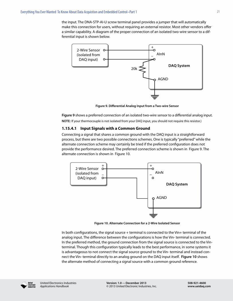
21Everything You Ever Wanted To Know About Data Acquistion and Embedded Control–Part 1
® United Electronics IndustriesApplications Handbook
Version: 1.0 — December 2013© 2013 United Electronic Industries, Inc.
508-921-4600www.ueidaq.com
the input. The DNA-STP-AI-U screw terminal panel provides a jumper that will automatically make this connection for users, without requiring an external resistor. Most other vendors offer a similar capability. A diagram of the proper connection of an isolated two-wire sensor to a dif-ferential input is shown below.
2-Wire Sensor(isolated from
DAQ input)AInN
DAQ System
AGND
20k
+
–
Figure 9. Differential Analog Input from a Two-wire Sensor
Figure 9 shows a preferred connection of an isolated two-wire sensor to a differential analog input.NOTE: If your thermocouple is not isolated from your DAQ input, you should not require this resistor.)
1.15.4.1 Input Signals with a Common GroundConnecting a signal that shares a common ground with the DAQ input is a straightforward process, but there are two possible connections schemes. One is typically “preferred” while the alternate connection scheme may certainly be tried if the preferred configuration does not provide the performance desired. The preferred connection scheme is shown in Figure 9. The alternate connection is shown in Figure 10.
2-Wire Sensor(isolated from
DAQ input)AInN
DAQ System
AGND
+
–
+
–
Figure 10. Alternate Connection for a 2-Wire Isolated Sensor
In both configurations, the signal source + terminal is connected to the Vin+ terminal of the analog input. The difference between the configurations is how the Vin- terminal is connected. In the preferred method, the ground connection from the signal source is connected to the Vin- terminal. Though this configuration typically leads to the best performance, in some systems it is advantageous to not connect the signal source ground to the Vin- terminal and instead con-nect the Vin- terminal directly to an analog ground on the DAQ input itself. Figure 10 shows the alternate method of connecting a signal source with a common ground reference.
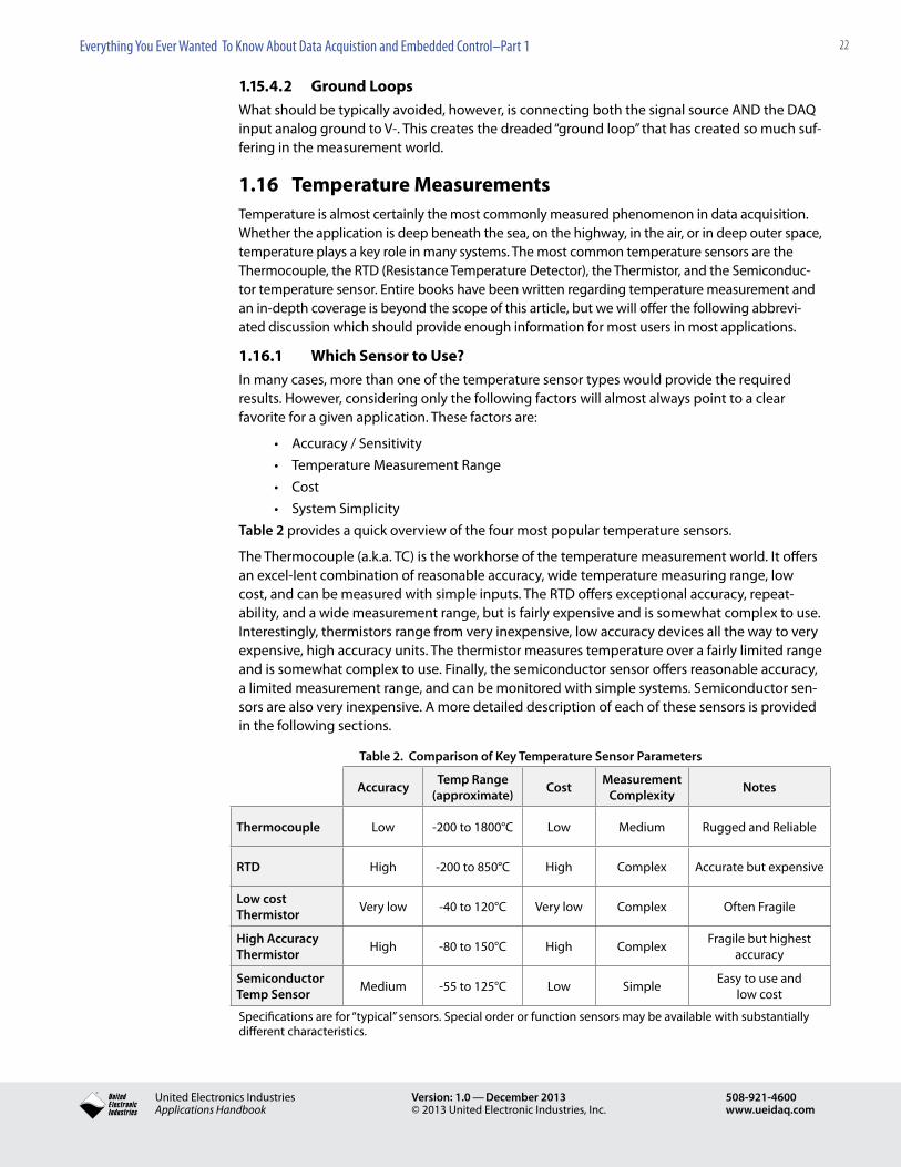
22Everything You Ever Wanted To Know About Data Acquistion and Embedded Control–Part 1
® United Electronics IndustriesApplications Handbook
Version: 1.0 — December 2013© 2013 United Electronic Industries, Inc.
508-921-4600www.ueidaq.com
1.15.4.2 Ground LoopsWhat should be typically avoided, however, is connecting both the signal source AND the DAQ input analog ground to V-. This creates the dreaded “ground loop” that has created so much suf-fering in the measurement world.
1.16 Temperature MeasurementsTemperature is almost certainly the most commonly measured phenomenon in data acquisition. Whether the application is deep beneath the sea, on the highway, in the air, or in deep outer space, temperature plays a key role in many systems. The most common temperature sensors are the Thermocouple, the RTD (Resistance Temperature Detector), the Thermistor, and the Semiconduc-tor temperature sensor. Entire books have been written regarding temperature measurement and an in-depth coverage is beyond the scope of this article, but we will offer the following abbrevi-ated discussion which should provide enough information for most users in most applications.
1.16.1 Which Sensor to Use?In many cases, more than one of the temperature sensor types would provide the required results. However, considering only the following factors will almost always point to a clear favorite for a given application. These factors are:
• Accuracy/Sensitivity• TemperatureMeasurementRange• Cost• SystemSimplicity
Table 2 provides a quick overview of the four most popular temperature sensors.
The Thermocouple (a.k.a. TC) is the workhorse of the temperature measurement world. It offers an excel-lent combination of reasonable accuracy, wide temperature measuring range, low cost, and can be measured with simple inputs. The RTD offers exceptional accuracy, repeat-ability, and a wide measurement range, but is fairly expensive and is somewhat complex to use. Interestingly, thermistors range from very inexpensive, low accuracy devices all the way to very expensive, high accuracy units. The thermistor measures temperature over a fairly limited range and is somewhat complex to use. Finally, the semiconductor sensor offers reasonable accuracy, a limited measurement range, and can be monitored with simple systems. Semiconductor sen-sors are also very inexpensive. A more detailed description of each of these sensors is provided in the following sections.
Table 2. Comparison of Key Temperature Sensor Parameters
Accuracy Temp Range (approximate) Cost Measurement
Complexity Notes
Thermocouple Low -200 to 1800°C Low Medium Rugged and Reliable
RTD High -200 to 850°C High Complex Accurate but expensive
Low cost Thermistor Very low -40 to 120°C Very low Complex Often Fragile
High Accuracy Thermistor High -80 to 150°C High Complex Fragile but highest
accuracy
Semiconductor Temp Sensor Medium -55 to 125°C Low Simple Easy to use and
low cost
Specifications are for “typical” sensors. Special order or function sensors may be available with substantially different characteristics.

23Everything You Ever Wanted To Know About Data Acquistion and Embedded Control–Part 1
® United Electronics IndustriesApplications Handbook
Version: 1.0 — December 2013© 2013 United Electronic Industries, Inc.
508-921-4600www.ueidaq.com
1.16.2 ThermocouplesThe thermocouple (a.k.a. TC) is the most commonly used temperature sensor. It offers a combination of good accuracy, wide measurement range, low cost, and simple usage. The thermocouple is also available in a wide variety of formats including bare wire, stainless steel probes, hypodermic probes, and bolt-on units. The wide variety of thermocouple configura-tions makes it easy to mechanically adapt the sensor to the application.
The thermocouple’s ability to sense temperature is based on the so-called “Seebeck Effect”, discovered by Thomas Seebeck in 1821. The Seebeck Effect, also known as the thermoelectric effect, states that any electrical conductor will produce a voltage when subjected to a thermal gradient.
The magnitude and polarity of the voltage produced varies with the type of metal used for the conductor and the magnitude of the thermal gradient. A thermocouple is constructed by connecting two conductors, composed of dissimilar metals. Since the second conductor senses the same thermal gradient as the first, it also produces a voltage. This voltage, how-ever, is different from that of the first conductor because it is made from a different metal. The small difference between the two voltages, which is typically in the millivolt range, is used for measurement of the thermal gradient. A simple way1 to think of a thermocouple is to think of it as any connection of two dissimilar metals that produces an output voltage related to the junction temperature.
1.16.2.1 Thermocouple TypesAny combination of dissimilar metals creates a thermocouple when they are connected. Wrap a copper wire around a steel coat hanger and you have created a thermocouple. However, you would have little idea what the characteristics of your coat hanger TC would be. In order to use it to make any sort of reasonably accurate temperature measurement, you would have to characterize it by measuring the output voltage at various temperatures. This would be a long and laborious task, and since you could not be assured the next coat hanger you wanted to use had an identical chemical composition, you could not use the same characteristics for the next TC you created.
To simplify the use of TCs, the industry has created a number of standard thermocouples, with standard chemistries that provide predictable and repeatable measurements. These TCs are typically designated by a single letter. Popular thermocouple types include: J, K, T, E, R, S, and N. There are also a number of less popular, but still well defined types available. Though many of the TCs offer similar capabilities, they each offer a different combination of scale factor, overall accuracy, measurement temperature range, and cost. Table 3 (page 24) describes the more popular types of TCs and their defining characteristics.
1 Though not strictly true from a physics point of view, this description of a thermocouple is commonly used and induces no error or confusion in the application of the device
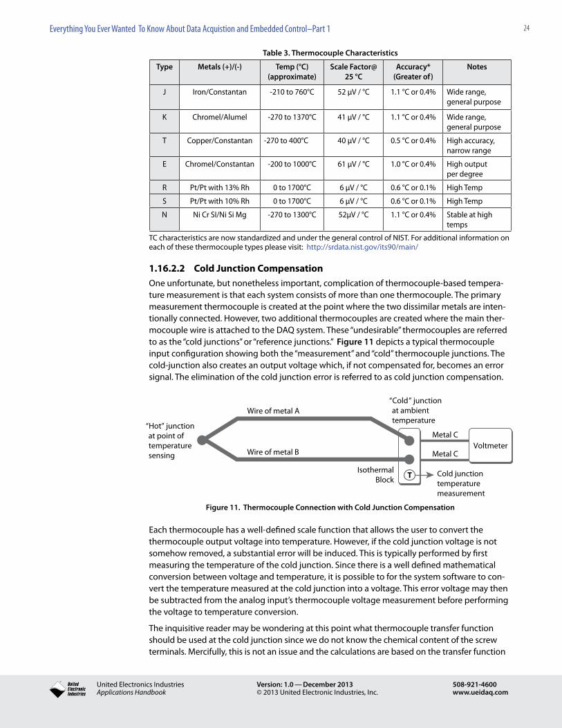
24Everything You Ever Wanted To Know About Data Acquistion and Embedded Control–Part 1
® United Electronics IndustriesApplications Handbook
Version: 1.0 — December 2013© 2013 United Electronic Industries, Inc.
508-921-4600www.ueidaq.com
Table 3. Thermocouple Characteristics
Type Metals (+)/(-) Temp (°C)(approximate)
Scale Factor@25 °C
Accuracy*(Greater of)
Notes
J Iron/Constantan -210 to 760°C 52 µV / °C 1.1 °C or 0.4% Wide range,general purpose
K Chromel/Alumel -270 to 1370°C 41 µV / °C 1.1 °C or 0.4% Wide range,general purpose
T Copper/Constantan -270 to 400°C 40 µV / °C 0.5 °C or 0.4% High accuracy, narrow range
E Chromel/Constantan -200 to 1000°C 61 µV / °C 1.0 °C or 0.4% High output per degree
R Pt/Pt with 13% Rh 0 to 1700°C 6 µV / °C 0.6 °C or 0.1% High Temp
S Pt/Pt with 10% Rh 0 to 1700°C 6 µV / °C 0.6 °C or 0.1% High Temp
N Ni Cr SI/Ni Si Mg -270 to 1300°C 52µV / °C 1.1 °C or 0.4% Stable at high temps
TC characteristics are now standardized and under the general control of NIST. For additional information on each of these thermocouple types please visit: http://srdata.nist.gov/its90/main/
1.16.2.2 Cold Junction CompensationOne unfortunate, but nonetheless important, complication of thermocouple-based tempera-ture measurement is that each system consists of more than one thermocouple. The primary measurement thermocouple is created at the point where the two dissimilar metals are inten-tionally connected. However, two additional thermocouples are created where the main ther-mocouple wire is attached to the DAQ system. These “undesirable” thermocouples are referred to as the “cold junctions” or “reference junctions.” Figure 11 depicts a typical thermocouple input configuration showing both the “measurement” and “cold” thermocouple junctions. The cold-junction also creates an output voltage which, if not compensated for, becomes an error signal. The elimination of the cold junction error is referred to as cold junction compensation.
VoltmeterMetal C
Metal C
Wire of metal B
Wire of metal A
IsothermalBlock
Cold junctiontemperaturemeasurement
“Cold” junction at ambient temperature “Hot” junction
at point of temperature sensing
T
Figure 11. Thermocouple Connection with Cold Junction Compensation
Each thermocouple has a well-defined scale function that allows the user to convert the thermocouple output voltage into temperature. However, if the cold junction voltage is not somehow removed, a substantial error will be induced. This is typically performed by first measuring the temperature of the cold junction. Since there is a well defined mathematical conversion between voltage and temperature, it is possible to for the system software to con-vert the temperature measured at the cold junction into a voltage. This error voltage may then be subtracted from the analog input’s thermocouple voltage measurement before performing the voltage to temperature conversion.
The inquisitive reader may be wondering at this point what thermocouple transfer function should be used at the cold junction since we do not know the chemical content of the screw terminals. Mercifully, this is not an issue and the calculations are based on the transfer function
25Everything You Ever Wanted To Know About Data Acquistion and Embedded Control–Part 1
® United Electronics IndustriesApplications Handbook
Version: 1.0 — December 2013© 2013 United Electronic Industries, Inc.
508-921-4600www.ueidaq.com
of the primary thermocouple. The law of intermediate metals1 states that a third metal, inserted between the two dissimilar metals of a thermocouple junction, will have no effect provided that the two junctions are at the same temperature. This allows us to ignore the chemistry of the screw terminals as well as all the intermediate metals between the screw terminals and the A/D converter. It is important to keep this in mind when we construct screw terminal panels and oth-er interconnection devices that will be used for thermocouples. If the two terminals where the TC is connected are not at the same temperature, the cold junction compensation algorithm will not provide an accurate result. Also, if the interconnection terminals are not at the same tem-perature as the cold junction temperature sensor, an error will be generated. UEI’s DNA-STP-AI-U and DNA-STP-207TC screw terminal panels make use of a device called an isothermal bar to min-imize these errors. The isothermal bar is typically a solid bar made of a good thermal conductor (usually aluminum or copper) placed in close proximity to the cold junction temperature sensor and the thermocouple connection terminals. Its high thermal conductivity, combined with its large thermal mass, combine to help keep the entire system at a single uniform temperature. The thermal mass of the bar also has the added advantage that it reduces the system’s suscepti-bility to fast, localized temperature changes caused by air currents as well as other phenomena.
1.16.2.3 LinearizationOnce the cold junction error voltage is removed, it is possible to accurately convert the TC output voltage into temperature. Though the output voltage over the temperature range of each TC type is well characterized, the relationship is not linear and requires that some math-ematics be applied. The TC to voltage conversions are available at the NIST website at: http://srdata.nist.gov/its90/main/
NIST provides the conversion in a look-up table which can be referred to for manual conver-sions or may be copied into a program or database to be referred to when required. The conversion is also provided as a high order (typically 5th or greater) polynomial. For example, to convert the voltage measured from a J-type TC into temperature (over the range of -210 to 760 °C) o, you may use the following equation.
T = a + bVin + cVin2 + dVin3 + eVin4 + f Vin5 + gVin6 + hVin7 + iVin8
where: a = 0.000000000000E + 00 b = 0.503811878150E - 01 c = 0.304758369300E - 04 d = -0.856810657200E - 07 e = 0.132281952950E - 09 f = -0.170529583370E - 12 g = 0.209480906970E - 15 h = -0.125383953360E - 18 j = 0.156317256970E - 22
Either the lookup table or the polynomial approximation may be used within the accuracy of the TC itself. Most computer programs will perform the conversion based on the polynomial approximation. (NIST also provides the reverse equation, which returns a voltage output for a temperature input. This equation is required to determine the Cold Junction error based upon the measurement of the screw terminal temperatures).
1 Based on this law, it is quite acceptable to make a thermocouple junction by soldering the two metals together as the solder will not affect the reading. In practice, however, thermocouple junctions are more frequently made by welding the two metals together (usually by capacitive discharge) because this en-sures that the performance is not limited by the melting point of solder.

26Everything You Ever Wanted To Know About Data Acquistion and Embedded Control–Part 1
® United Electronics IndustriesApplications Handbook
Version: 1.0 — December 2013© 2013 United Electronic Industries, Inc.
508-921-4600www.ueidaq.com
The good news in all of this is that most manufacturers provide the software required to au-tomatically convert the TC input voltage into temperature. One final note regarding the TC is that most systems will require users to dedicate an input channel to monitor the cold junction temperature sensor that can then be used by the program for CJC.
1.16.3 The RTD (or Resistance Temperature Detector)The RTD is most frequently used in applications where more temperature measurement ac-curacy is required than possible (or at least easily achievable) using thermocouples. In addition to excellent accuracy, the Platinum RTD (often referred to as a PRT or PRTD) offers exceptional stability, provides accurate measurements over the range of -200 °C to +850 °C, and is very resistant to corrosion or other chemical degradation .
Credit for the invention of the RTD is often given to Sir William Siemens (one of the brothers who founded the very successful Siemens Corporation) though it should more rightfully go to Sir Humphrey Davy. It was Davy who in 18211 discovered that the resistance of metals varied with temperature. However, 50 years later, Siemens began using Platinum as the basis of his RTDs and Pt remains overwhelmingly the element of choice in RTDs to this day.
By far the most common of all the RTDs are the 100-ohm Platinum units. These devices offer a resistance of precisely 100 ohms at 0°C. The two popular versions of the 100 ohm Pt RTD offer slightly different scale factors of 0.385 and 0.392 ohms per °C. The 0.385 version is typically called the “DIN” standard while the 0.392 version is commonly called the “American” standard. The various RTD types are typically designated by an α = 0.00385 and 0.00392. “v” actually rep-resents the average scale factor in ohms per ohm per °C. Since the base resistance is 100 ohms, the overall scale factors are 100 times, or 0.385 and 0.392 ohms per °C respectively.
Although the resistance of a platinum RTD varies directly with temperature over a wide range, it is not a perfectly linear relationship. To correct for inherent linearity errors, the industry uses the Callendar-Van Dusen equation and coefficients, developed many years ago by a British physicist named Hugh Callendar and later extended to temperatures below 0°C by Van Dusen. The Callendar-VanDusen equation for temperatures above 0°C is:
R1 R0 1 AT BT2 C T 100–( )T3+ + + ][=
where R0 is the resistance in ohms at 0°C
R1 is the resistance in ohms at 100°C
T is the temperature in °C
A, B, and C are the Callendar-Van Dusen coefficients, which are determined from resistance measurements at 0°C, 100°C, and 260°C and other empirical constants called α, δ, and β. The relationships between these constants and the Callendar-Van Dusen coefficients are as follows:
A= α + (α+β)/100 B= (-α+δ)/1002C = (-α + β)/1004
α = (R100 – R0)/(100*R0) β = Constant for T < 0°Cδ = [R0 (1 + α 260) – R260]/4.16 R0 α
The international standard for defining Class A and B performance of platinum RTDs is the IEC 751. The DIN 43760, BS-1904, JIS-C1604 all match the IEC 751 standard. Only platinum RTDs have an international standard.
1 Interestingly, this is the same year Seebeck made his discovery of the thermoelectric effect that is the basis for today’s thermocouples.

27Everything You Ever Wanted To Know About Data Acquistion and Embedded Control–Part 1
® United Electronics IndustriesApplications Handbook
Version: 1.0 — December 2013© 2013 United Electronic Industries, Inc.
508-921-4600www.ueidaq.com
The following chart shows the characteristic curves of resistance vs. temperature for two types of RTDs and, for comparison, the curve for a typical thermistor. The near linear curve for the platinum RTD is a major reason this type of RTD is the most used in industry.
Thermistor
Nickel RTD
Platinum RTD
-100 100v 200 300 400 500 600 700 0
1
2
3
4
5
6
Figure 12. Characteristic Curves of RTDs and Thermistors
The classical method of measuring change in resistance with respect to temperature is to use a Wheatstone bridge, such as shown below:
DVM
SG
Figure 13. Wheatstone Bridge
Because the Pt RTD has such a low value of resistance (100 ohms at 0°C), however, care must be taken to avoid errors caused by lead resistances.

28Everything You Ever Wanted To Know About Data Acquistion and Embedded Control–Part 1
® United Electronics IndustriesApplications Handbook
Version: 1.0 — December 2013© 2013 United Electronic Industries, Inc.
508-921-4600www.ueidaq.com
The bridge output voltage is an indirect indication of the RTD resistance. The bridge requires four connection wires, an external source, and three resistors that have a zero temperature coefficient. To avoid subjecting the three bridge-completion resistors to the same temperature as the RTD, the RTD is separated from the bridge by a pair of extension wires, as shown below:
DVM
RTD
RL
RL
Figure 14. Two-Wire RTD Circuit
The impedance of the extension wires, however, affects the temperature reading, introducing errors that may be significant. One way this effect can be minimized is by using a three-wire bridge configuration, as shown below:
DVM
SG
RL
RL
AB
C
DVM
SG
A
B
C
RL
RL
Figure 15. 3-wire RTD Circuit
In this configuration, if wires A and C are perfectly matched in length, their impedance effects cancel because each is in an opposite leg of the bridge. The third wire, B, acts as a sense lead, carries no current, and thus does not introduce any error in the measurement.
A better technique for eliminating errors caused by lead resistances is to use a four-wire RTD circuit with a current source and digital voltmeter, as shown below. This method avoids many problems associated with bridge circuits.
SG
i = 0+
–
4-Wire SG Measurement
i = 0
Figure 16. 4-wire RTD Circuit
29Everything You Ever Wanted To Know About Data Acquistion and Embedded Control–Part 1
® United Electronics IndustriesApplications Handbook
Version: 1.0 — December 2013© 2013 United Electronic Industries, Inc.
508-921-4600www.ueidaq.com
In a four-wire RTD circuit, the output voltage read by the DVM is directly proportional to RTD re-sistance, so only one conversion calculation is necessary. The three bridge-completion resistors are replaced by one reference resistor. The digital voltmeter measures only the voltage drop across the RTD and is insensitive to the length of the lead wires.
The one disadvantage of using a 4-wire RTD circuit is that it requires one more extension wire than the 3-wire bridge circuit.
1.16.3.1 Metal Film RTDsAnother type of RTD, the metal film RTD, has become more popular recently. It is constructed by depositing or screening a metal-glass slurry film on a small ceramic substrate, trimming the RTD with a laser beam, and then sealing the unit. The film RTD has higher values of resistance than other RTDs, smaller size, fast response, and low production cost. Although different expan-sion rates between the substrate and the deposited RTD material, such as platinum, can cause strain errors and stability problems, the advantages of the metal-film concept make the device increasingly popular.
1.16.3.2 Accessory Equipment for RTDsRTDs are frequently used with metal thermowells and other mechanical or chemical protection sheaths for harsh environments. Sometimes, however, more design effort is required for choos-ing the optimum protection device than for selecting the RTD sensor element.
1.16.4 The ThermistorA thermistor is a highly non-linear temperature sensing device whose resistance varies with temperature. They are available in two basic types: PTC (positive temperature coefficient) or NTC (negative temperature coefficient).The PTC thermistor is sometimes called a Posistor, but the NTC is always called a thermistor. Figure 12 on page 29 showing characteristic curves of RTDs and thermistors illustrates how non-linear a thermistor curve is. The thermistor was invented and patented by Samuel Ruben in 1930.
An NTC thermistor is composed of a sintered semiconductor material with a resistance that decreases significantly with a small change in temperature. A thermistor is one of the most ac-curate types of temperature sensors, with typical accuracies in the ±0.1 or ±0.2 °C range, but its application is typically limited to the range of 0°C to 100°C.
Because of the highly non-linear characteristic of the thermistor, the instrument or DAQ system used to read the temperature must linearize the measurement. Some manufacturers, however, do produce thermistors (at higher cost) with built-in linearization components that make the unit act as a linear device.
1.16.4.1 Linearization — Steinhart-Hart EquationFor accurate temperature measurements, the Steinhart-Hart equation is used as a third-order approximation, as follows:
1T--- A B Rln( ) C Rln( ) 3+ +=
where
T is the absolute temperature in Kelvin and A, B, and C are constants that can be determined by measuring three sets of resistance and temperature values during calibration.
Most thermistors are NTC units in which resistance decreases with an increase in temperature. They are specified according to their nominal resistance at 25°C, which is typically in the range from 250 ohms to 100 kohms.

30Everything You Ever Wanted To Know About Data Acquistion and Embedded Control–Part 1
® United Electronics IndustriesApplications Handbook
Version: 1.0 — December 2013© 2013 United Electronic Industries, Inc.
508-921-4600www.ueidaq.com
1.16.4.2 Self-Heating EffectsWhen current flows through a thermistor, it generates heat that raises the temperature of the themistor above the surrounding environment. If the thermistor is being used to measure tem-perature, the self-heating of the unit can introduce an error if not corrected.
1.17 Strain (& Stress) Measurements1.17.1 Introduction to the Strain GaugeThe Strain Gauge (a.k.a. Strain Gage) is one of the most commonly measured devices in data acquisition and DAQ systems. Strain is often measured as the actual parameter of interest. If the application is actually interested in how much an object expands, contracts, or twists, the desired measurement is strain.
Strain is also frequently measured as an intermediate means to measure stress, where stress is the force required to induce a strain. Perhaps the most common examples of this translated measurement are load cells, where the strain of a known, well characterized metallic bar is measured, though the actual output scale factor of the cell is in units of force (e.g. pounds or newtons). The stress/strain relationship is well defined in many materials in certain configura-tions, making the conversion from strain into stress a straight-forward mathematical calcula-tion. Making matters easier still is that for many materials, including virtually all metals, the rela-tionship between stress and strain when the stress is applied in pure tension or compression is linear. The linearity of the relationship is referred to as Hooke’s law, while the actual coefficient that describes the relationship is commonly referred to as either the modulus of elasticity or Young’s modulus.
Whether stress or strain is the actual measurement of interest, the mechanics of the strain gauge and the electronics required to make the measurement are virtually identical. To create a simple strain gauge, you need only firmly attach a length of wire to the object being strained. If attached in-line with the strain as the object lengthens under tension, the wire too is length-ened. As the wire length increases so does its resistance. On the other hand, if the strained object is compressed, the length of the wire decreases, and there is a corresponding change in the wire’s resistance. Measure the resistance change and you have an indication of the strain changes of your object. Of course, the scale factor needed to convert the resistance change into strain would have to be determined some how, and it would not be a trivial process. Also, the resistance change for a small strain change would be miniscule, making the measurement a difficult one.
Today’s strain gauge manufacturers have solved both the scale factor and, to a certain extent, the magnitude of resistance change issues. To increase the output (resistance change) per unit of strain, today’s strain gauges are typically created by placing multiple “wires” in a zig-zag configuration (see Figure 17) A strain gauge with 10 zigs and 10 zags would effectively increase the output scale factor by a factor of 20 over the single wire example. For a simple application, all you need to do is align the strain gauge so the “long” elements are in parallel to the direction of strain to measure, and affix the gauge with an appropriate adhesive.
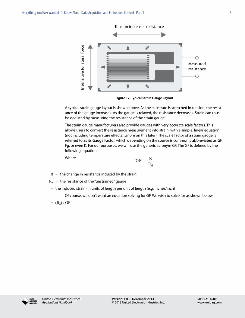
31Everything You Ever Wanted To Know About Data Acquistion and Embedded Control–Part 1
® United Electronics IndustriesApplications Handbook
Version: 1.0 — December 2013© 2013 United Electronic Industries, Inc.
508-921-4600www.ueidaq.com
Measuredresistance
Tension increases resistance
Inse
nsiti
ve to
late
ral f
orce
Figure 17. Typical Strain Gauge Layout
A typical strain gauge layout is shown above. As the substrate is stretched in tension, the resist-ance of the gauge increases. As the gauge is relaxed, the resistance decreases. Strain can thus be deduced by measuring the resistance of the strain gauge
The strain gauge manufacturers also provide gauges with very accurate scale factors. This allows users to convert the resistance measurement into strain, with a simple, linear equation (not including temperature effects…more on this later). The scale factor of a strain gauge is referred to as its Gauge Factor, which depending on the source is commonly abbreviated as GF, Fg, or even K. For our purposes, we will use the generic acronym GF. The GF is defined by the following equation:
WhereGF R
R0------=
R = the change in resistance induced by the strain
Ro = the resistance of the “unstrained” gauge
= the induced strain (in units of length per unit of length (e.g. inches/inch)
Of course, we don’t want an equation solving for GF. We wish to solve for as shown below.
= (Ro) / GF
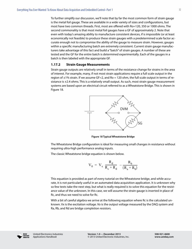
32Everything You Ever Wanted To Know About Data Acquistion and Embedded Control–Part 1
® United Electronics IndustriesApplications Handbook
Version: 1.0 — December 2013© 2013 United Electronic Industries, Inc.
508-921-4600www.ueidaq.com
To further simplify our discussion, we’ll note that by far the most common form of strain gauge is the metal foil gauge. These are available in a wide variety of sizes and configurations, but most have two common threads. First, most are offered with Ro=120, 350 or 1000 ohms. The second commonality is that most metal foil gauges have a GF of approximately 2. Note that even with today’s amazing ability to manufacture consistent devices, if is impossible (or at least economically not feasible) to produce these strain gauges with a predetermined scale factor ac-curate enough not to compromise the ability of the gauge to measure strain. However, gauges within a specific manufacturing batch are extremely consistent. Current strain gauge manufac-turers take advantage of this fact and build a “batch” of strain gauges. A number of these are tested and the GF for the entire batch is determined experimentally. Each of the gauges in a batch is then labeled with the appropriate GF.
1.17.2 Strain Gauge MeasurementsStrain gauge outputs are relatively small in terms of the resistance change for strains in the area of interest. For example, many, if not most strain applications require a full scale output in the region of ±1% strain. If we assume GF=2, and Ro = 120 ohm, the full scale output in terms of re-sistance is ±2.4 ohms. This is a relatively small output. As such, most strain gauge measurement systems are based upon an electrical circuit referred to as a Wheatstone Bridge. This is shown in Figure 18.
DVM
SG
Figure 18 Typical Wheatstone Bridge
The Wheatstone Bridge configuration is ideal for measuring small changes in resistance without requiring ultra-high performance analog inputs.
The classic Wheatstone bridge equation is shown below.
V0 VxRd
Rc Rd+-------------------
RbRa Rb+( )
-----------------------–=
This equation is provided as part of every tutorial on the Wheatstone bridge, and while accu-rate, it is not particularly useful in an automated data acquisition application. It is unknown why so few texts take the next step, but what is really required is to solve this equation for the resist-ance value of the unknown. In this case, we will assume the strain gauge is inserted in place of Rc, and thus we need to solve for Rc.
With a bit of careful algebra we arrive at the following equation where Rc is the calculated un-known. Vx is the excitation voltage. Vo is the output voltage measured by the DAQ system and Ra, Rb, and Rd are bridge completion resistors.

33Everything You Ever Wanted To Know About Data Acquistion and Embedded Control–Part 1
® United Electronics IndustriesApplications Handbook
Version: 1.0 — December 2013© 2013 United Electronic Industries, Inc.
508-921-4600www.ueidaq.com
RcRd RdV0( ) Vx⁄ RdRb( ) Ra Rb+( )⁄– )(–
V0 Vx⁄ Rb Ra Rb+( )⁄+--------------------------------------------------------------------------------------------------=
It’s not a pretty equation, and is a bear to calculate repetitively by hand, but who calculates things by hand these days? It really is quite easy to implement this equation in Excel, LabView, or any programming language. And once you have it, you won’t need to write it again. Also note that there is no linear approximation in this equation, so it will work for larger changes, if the bridge is out of balance. In many cases, you may also simplify the equation because Ra = Rb. In this case the equation for Rc drops to
RcRd Vx 2V0–( )
2V0 Vx+----------------------------------=
We may know the static/unloaded value of Rc from a prioi knowledge, or we may need to calculate Rc based upon the measurement. However, once we have the initial value of Rc (we’ll call it Rco), we can then go on to solve our equation for the strain gauge. Recalling our original strain equation,
RcR R0⁄
GF--------------=
We can now insert the values for Rc. Once again assuming Rco is the unstrained condition, and based upon our measurement and the calculations above, Rc1 is the resistance measurement of Rc when strained. GF again is the Gain Factor constant (typically ~ 2.0).
Rc1 Rc0–( ) Rc0⁄ GF( )⁄= Rc1 Rc0–( ) Rc0⁄ GF( )⁄=
or
Rc Rc1 Rc0 1–( )⁄ GF( )⁄=
If the variable of interest is Stress rather than Strain, we can now proceed to calculate it. In the simplest case, with a sample in tension and/or compression and with a known Modulus of elas-ticity (a.k.a. Young’s Modulus), you may calculate Stress with the following equation:
σ εE---=
where τ is the stress, ε is the strain, and E is the Modulus of Elasticity. Recognizing that stress is defined as the Force per unit of area, we can generalize the above equation into:
F / A = ε / E
where F is the force applied and A is the cross sectional area of the object under test. If the Modulus of Elasticity is known and the cross sectional area of the object under test is known, we can use the strain gauge to determine the force applied.
F εAE
-------=
The ability to determine force with a strain gauge is the basis for almost all electronic scales and load cells.

34Everything You Ever Wanted To Know About Data Acquistion and Embedded Control–Part 1
® United Electronics IndustriesApplications Handbook
Version: 1.0 — December 2013© 2013 United Electronic Industries, Inc.
508-921-4600www.ueidaq.com
1.17.3 Temperature Effects in Strain MeasurementThough complete coverage of the impact of temperature on strain measurements is beyond the scope of this document, it is too important a topic not to be addressed. Temperature ad-versely impacts strain measurements in many ways, though three are of primary concern.
• Thedeviceorobjectstudiedwillalmostalwayshaveanon-zerocoefficientofthermal expansion. Unless compensated for, changes in temperature will cause the item to which the strain gauge is attached to expand or contract, which is then indicated as a change in strain.
• Thematerialsofthestraingaugeitselfhaveanon-zerocoefficientofthermalexpansion. Changes in temperature will cause the strain gauge itself to expand or contract, independent of any strain in the part to which it is attached.
• Thewiringandthestraingaugeitselfwillhaveanon-zeroTemperatureCoef-ficient of Resistance. That is, as the temperature changes, the resistance of the strain gauge and connecting wires will change independently of any change in strain. (For example, copper wire resistance changes at approximately 3900 ppm per °C (.393% /°C).)
1.17.4 Thermal Expansion/Contraction IssuesSome texts treat the first two items as the same effect. After all, if the coefficients of expansion of the gauge and the item under test are the same, they will contract or expand at the same rates in response to a temperature change. In this case, a change in system temperature would not cause any change in the indicated strain, except that based on the gauge’s temperature coefficient of resistance. It’s important to note that in some applications, it may be desirable or even critical that strain induced by temperature changes be noted. Envision an application where a “hot section” turbine blade is being tested to ensure proper clearance between the blade tip and the surrounding shroud. It’s important to know how much the blade has elon-gated based upon temperature in addition to the centrifugal force of rotation.
On the other hand, if the parameter of interest is really stress, or its close relative, force, any strain caused by temperature changes would induce a true error in the result. A strain gauge used to measure the “g” forces on a supersonic aircraft wing skin might see temperatures from -45°C to 200 °C. If the g-force information was critical to not overstressing the wing, you’d cer-tainly not want significant temperature-induced error. In a more simple case, the load cell used to measure the force placed on a postal scale should not induce errors simply because the scale is next to the window on a sunny summer day!
Most applications fall into the second category, where the key measurement parameter is really stress, and the ideal system would be not to recognize any changes caused by thermal expan-sion or contraction. Like most engineering challenges, there is more than one way to skin this proverbial cat. They are: (1) Calculate the error and eliminate it mathematically, (2) Match the strain gauge to the part, (3) Use an identical strain gauge in another leg of the bridge.
1.17.5 Calculate the Error and Eliminate It MathematicallyIf you know the actual difference in coefficients of thermal expansion between the strain gauge and the part being tested, it’s theoretically possible to mathematically eliminate the error caused by changes in temperature. Of course, to do this, you also need to measure the temperature accurately at the strain gauge installation. The strain gauge expansion coefficients however, are not generally available from the manufacturer as they tend to change from batch to batch. Though possible, compensating for temperature effects using only this “calculated” method is seldom done.
More common, but still not very common, a pseudo-calculated method is performed. Rather than use a priori predicted coefficients to calculate the differential strain induced by tempera-

35Everything You Ever Wanted To Know About Data Acquistion and Embedded Control–Part 1
® United Electronics IndustriesApplications Handbook
Version: 1.0 — December 2013© 2013 United Electronic Industries, Inc.
508-921-4600www.ueidaq.com
ture changes, it is possible to determine the function experimentally. The word function is used intentionally, as the actual strain versus temperature curve is infrequently linear, especially over large temperature changes. However, if the application allows the system’s strain vs. tempera-ture curve to be determined experimentally, it becomes fairly straightforward to remove the error mathematically.
1.17.6 Match the Strain Gauge to the Part TestedThe use of different alloys/metals allows manufacturers to provide strain gauges designed to match the thermal expansion/contraction behavior of a wide variety of materials commonly subject to strain (and stress) testing. This type of gauge is referred to as a “Self Temperature Compensated” (or STC) strain gauge. These STC gauges are available from a variety of manufac-turers and are specified for use on a wide assortment of part materials. As you might imagine, the more common a metal, the better the chances are there is an STC gage that matches. How-ever, you may count on being able to find a good match for such materials as aluminum, brass, cast iron, copper, carbon steel, stainless steel, titanium and many more.
Though the match between the STC gauge and the part under test may not be perfect, it will typically be accurate enough from freezing to well past the boiling point of water. For more details on the precise accuracy to expect, you should contact your strain gauge manufacturer.
1.17.7 Use an Identical Strain Gauge in Another Leg of the BridgeDue to the ratiometric nature of the Wheatstone bridge, a second, unstrained gauge (often re-ferred to as a “dummy” gauge) placed in another leg of the bridge will compensate for tempera-ture induced strain. Note that the dummy gauge should be identical to the “measuring” gauge and should be subject to the same environment.
Strain gauges tend to be small, and have short thermal time constants (i.e., their temperature changes very quickly in response to a temperature change around them), while the part under test may have substantial thermal mass and may change temperature slowly. For this reason, it is good practice to mount the dummy gauge adjacent to gauge being measured. However, it should be attached in such a way as not to be subjected to the induced strain of the tested part.
In some cases, with relatively thin subjects and when measuring bending strain (as opposed to pure tensile or compressive strain), it may be possible to mount the dummy gauge on the opposite side of a bar or beam. In this case, the temperature impact of the gauges is eliminated and the scale factor of the output is effectively doubled.
1.17.8 Quarter, Half and Full BridgesStrain gauges and measurement devices based upon strain gauges (e.g., load cells) can be con-figured in three different configurations. These are referred to as Quarter, Half and Full Bridges.
DVM
SG
RL
RL
Figure 19 Quarter Bridge Strain Gauge
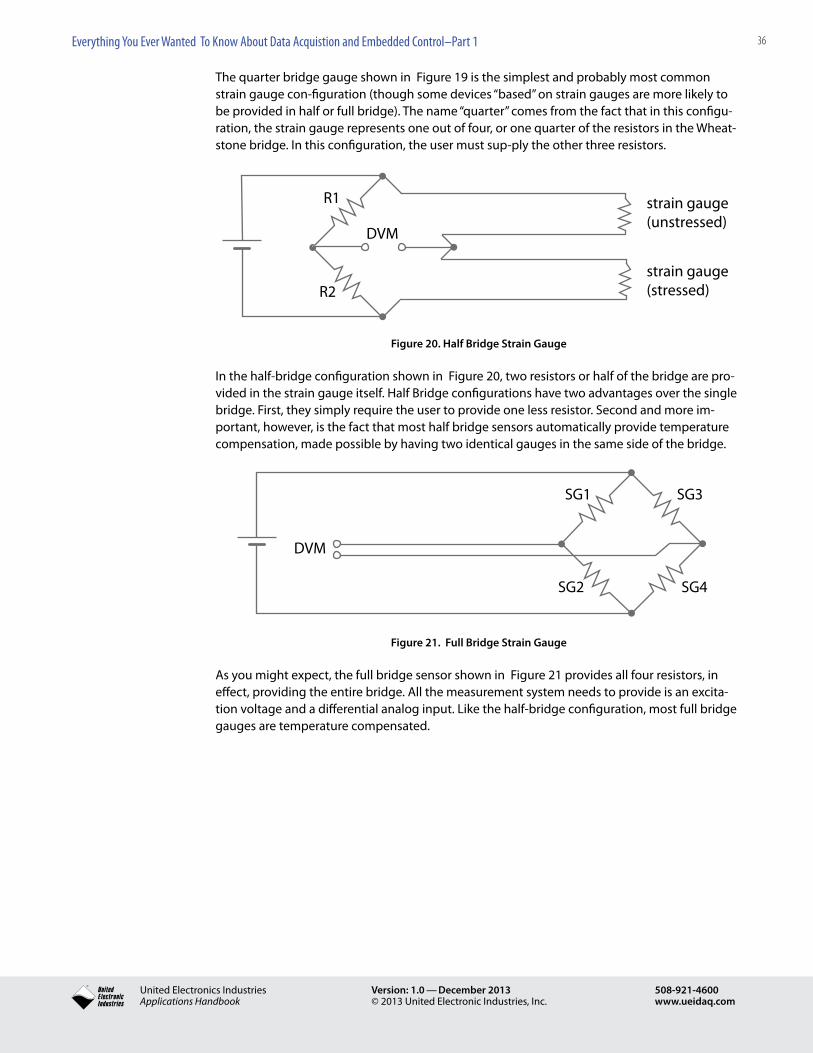
36Everything You Ever Wanted To Know About Data Acquistion and Embedded Control–Part 1
® United Electronics IndustriesApplications Handbook
Version: 1.0 — December 2013© 2013 United Electronic Industries, Inc.
508-921-4600www.ueidaq.com
The quarter bridge gauge shown in Figure 19 is the simplest and probably most common strain gauge con-figuration (though some devices “based” on strain gauges are more likely to be provided in half or full bridge). The name “quarter” comes from the fact that in this configu-ration, the strain gauge represents one out of four, or one quarter of the resistors in the Wheat-stone bridge. In this configuration, the user must sup-ply the other three resistors.
R1
DVM
strain gauge(unstressed)
strain gauge(stressed)R2
Figure 20. Half Bridge Strain Gauge
In the half-bridge configuration shown in Figure 20, two resistors or half of the bridge are pro-vided in the strain gauge itself. Half Bridge configurations have two advantages over the single bridge. First, they simply require the user to provide one less resistor. Second and more im-portant, however, is the fact that most half bridge sensors automatically provide temperature compensation, made possible by having two identical gauges in the same side of the bridge.
SG1 SG3
SG2 SG4
DVM
Figure 21. Full Bridge Strain Gauge
As you might expect, the full bridge sensor shown in Figure 21 provides all four resistors, in effect, providing the entire bridge. All the measurement system needs to provide is an excita-tion voltage and a differential analog input. Like the half-bridge configuration, most full bridge gauges are temperature compensated.

37
® United Electronics IndustriesApplications Handbook
Version: 1.0 — December 2013© 2013 United Electronic Industries, Inc.
508-921-4600www.ueidaq.com
2 “Other” types of DAQ I/O HardwareThis section describes the “other common” types of DAQ I/O — devices such as Analog Outputs, Digital Inputs, Digital Inputs, Counter/Timers, and Special DAQ functions, which covers such de-vices as Motion I/O, Synchro/Resolvers, LVDT/RVDTs, String Pots, Quadrature Encoders, and ICP/IEPE Piezoelectric Crystal Controllers. It also covers such topics as communications interfaces, timing, and synchronization functions.
2.1 Analog OutputsAnalog or D/A outputs are used for a variety of purposes in data acquisition and control sys-tems. To properly match the D/A device to your application, it is necessary to consider a variety of specifications, which are listed and explained below.
2.11 Number of ChannelsAs it’s a fairly obvious requirement, we won’t spend much time on it. Make sure you have enough outputs to get the job done. If it’s possible that your application may be expanded or modified in the future, you may wish to specify a system with a few “spare” outputs. At the very least, be sure you can add outputs to the system down the road without major difficulty.
2.1.2 ResolutionAs with A/D channels, the resolution of a D/A output is a key specification. The resolution de-scribes the number or range of different possible output states (typically voltages or currents) the system is capable of providing. This specification is almost universally provided in terms of “bits”, where the resolution is defined as 2(# of bits). For example, 8-bit resolution corresponds to a resolution of one part in 28 or 256. Similarly, 16-bit resolution corresponds to one part in 216 or 65, 536. When combined with the output range, the resolution determines how small a change in the output may be commanded. To determine the resolution, simply divide the full scale range of the output by its resolution. A 16-bit output with a 0-10 Volt full scale output pro-vides 10 V/216 or 152.6 microvolts resolution. A 12-bit output with a 4-20 mA full scale provides 16 mA/212 or 3.906 uA resolution.
Out
put
Vol
tage
Value Written to D/A Value Written to D/A
Out
put
Vol
tage
Out
put
Vol
tage
Value Written to D/A
OutputOffsetError
Actual OutputvvVoltage
Gain ReferenceError
Ideal Output
Offset Error Gain/Reference Error Non-Linearity Error
Ideal Output
Actual OutputVoltage
Ideal Output
IntregalNonliniearityError (INL)
Figure 1. Error Factors.
The standard resolution of most DAQ analog output interfaces is 16-bit and you will also see some devices with 12-bit resolution. Though it is now common to see analog inputs with 20 or 24-bit resolution, requiring resolutions of greater than 16-bits is fairly rare in applications where DC accuracy is important, but is common in AC applications such as in the audio output ”world”.

38Everything You Ever Wanted To Know About Data Acquistion and Embedded Control–Part 2
® United Electronics IndustriesApplications Handbook
Version: 1.0 — December 2013© 2013 United Electronic Industries, Inc.
508-921-4600www.ueidaq.com
2.1.3 Accuracy Though accuracy is often equated to resolution, they are not the same. An analog output with a one microvolt resolution does not does not necessarily (or even typically) mean the output is accurate to one microvolt resolution. Outside of audio outputs, D/A system accuracy is typically on the order of a few LSBs. However, it is important to check this specification as not all analog output systems are created equal. The most significant and common error contri-butions in analog output systems are Offset, Gain/Reference, and Linearity errors. These are depicted graphically above in Figure 1 – Error Factors.
2.1.3 AccuracyThough accuracy is often equated to resolution, they are not the same. An analog output with a one microvolt resolution does not does not necessarily (or even typically) mean the output is accurate to one microvolt resolution. Outside of audio outputs, D/A system accuracy is typically on the order of a few LSBs. However, it is important to check this specification as not all analog output systems are created equal. The most significant and common error contri-butions in analog output systems are Offset, Gain/Reference, and Linearity errors. These are depicted graphically above (on page 40) in Figure 1 – Error Factors.
The primary contributors of a D/A output are Output Offset, Gain Error, Reference Error, and Non-Linearity. Note that both Gain and Reference are shown on a single graph as they both contribute to an undesired change of slope in the output diagram. More detailed descriptions of each of these errors is provided in a variety of articles, both published and on the web. A detailed description of each of these factors can be readily retrieved by simply typing the phrase into your favorite search engine. The important thing to remember is that these errors are additive, and to determine the overall system accuracy, you must account for the contribu-tions from all error sources. There are additional contributing error factors that must be taken into account that are more application-specific than product-specific. Errors may be gener-ated by the D/A channel output impedance as well as “IR” errors induced in the field wiring (as neither the current flowing in the field wiring nor the resistance of the wiring is zero.
Both output impedance and IR errors manifest themselves when the D/A channel is required to drive a significant output current. Ohm’s law (V=IR) dictates that the error generated will be the product of the channel output impedance, plus the resistance in the field wiring, divided by the cur-rent flowing. The equation for this error is shown below:
Resistance error = (D/A output impedance + field wiring resistance)/current flow
In many applications, the device the output is driving is high impedance and the current is so low this error is negligible. However, many analog outputs are capable of driving five or ten milliamps, or even more. If your application requires output drive in the milliamp range or higher, be sure to check this error. D/A output impedances are typically on the order of 0.1 ohm. A 10 mA signal flowing through 0.1 ohm generates a 1 mV error signal. The resolution of a ±10 Volt, 16-bit, analog out-put channel is 305 uV, so that 1 mV error actually represents an error of over 3 LSBs.

39Everything You Ever Wanted To Know About Data Acquistion and Embedded Control–Part 2
® United Electronics IndustriesApplications Handbook
Version: 1.0 — December 2013© 2013 United Electronic Industries, Inc.
508-921-4600www.ueidaq.com
Table 1: Resistance and IR drop of Copper Wire Cable
IR Voltage Drop 1 mA Current
IR Voltage Drop 10 mA Current
Wire Size Ohms per 100 feet
10’ Cable 100’ Cable 10’ Cable 100’ Cable
16ga 0.41 0.041mV 0.41mV 0.41mV 4.1 mV
20ga 1.04 0.104 1.04 1.04 10.04
22ga 1.65 0.165 1.65 1.65 16.5
2.62 0.262 0.262 2.62 2.62 26.2
26ga 4.16 0.416 4.16 4.16 41.6
30ga 10.5 1.05 10.5 10.5 105
NOTE: All voltage errors are in millivolts (mV). Cable length is total length, including both output and return cables.
The table above shows the resistance per foot of a number of common solid copper sizes as well as the IR induced error at 1 mA and 10 mA with connection wire lengths of 10 and 100 feet. Note that 1 LSB of a 16-bit analog output with a ±10 Volt full scale output is 0.305 mV. The IR losses are often significant.
More insidious than the channel output impedance is the IR drop of the field wiring. While many people simply assume the resistance is low enough to have no impact, this is often not the case. Note that 26 and 30 gauge, single conductor, copper wire has resistance of about 0.026 ohm per foot and 0.105 ohm per foot, respectively. If your output is driving 5 mA, and is connected by 50 feet of 30 gauge wire, you’ll see an IR drop in the field wiring of about 53 mV (don’t forget the IR drop occurs in both directions). Table 1 above shows the IR error in a num-ber of different combinations of wire size, output current, and cable length.
There are really three options for reducing this IR drop error. First, you can minimize the dis-tance between the analog output and the device it is driving. Second, you can increase the size of the wire to reduce the series resistance. However, it is not always possible to do either of these, which leads to option three, use a board with “Sense” leads or connections. The Sense capability is designed to automatically compensate for IR losses in the system. Basically, the sense leads are connected in parallel with the “main” analog output leads, but do not conduct any current. This allows the D/A converter to adjust its output so the voltage at the device or load is at the desired level, and not the output at the D/A converts itself. Many analog output devices, and in particular, those designed to drive higher currents (>5 or 20 mA), will have sense leads that may be used.
2.1.4 MonotonicityThough it’s common sense to assume that if you command your output to go to a higher voltage, it will, regardless of the overall accuracy. However, this is not necessarily the case. D/A converters exhibit an error called differential non-linearity (DNL).
In essence, DNL error represents the variation in output “step size” between adjacent codes. Ideally, commanding the output to increase by 1LSB,would cause the output to change by an amount equal to the overall output resolution. However, D/A converters are not perfect and increasing the digital code written to a D/A by one may cause the output to change .5 LSB, 1.3 LSB, or any other arbitrary number.
A D/A/channel is said to be monotonic if every time you increase the digital code written to the D/A converter, the output voltage does indeed increase. If the D/A converter DNL is less than ±1 bit, the converter will be monotonic. If not, commanding a higher output voltage

40Everything You Ever Wanted To Know About Data Acquistion and Embedded Control–Part 2
® United Electronics IndustriesApplications Handbook
Version: 1.0 — December 2013© 2013 United Electronic Industries, Inc.
508-921-4600www.ueidaq.com
could in fact cause the output to drop. In control applications, this can be very problematic as it becomes theoretically possible for the system to “lock” onto a false set point, distant from the one desired.
2.1.5 Output TypeUnlike analog inputs, which come in a myriad of sensor-specific input configurations, analog out-puts typically come in two flavors, voltage output and current output. Be sure to specify the right type for your system. Some devices offer a mixture of voltage and current outputs, though most offer only a single type. If your system requires both, you may want to consider a current output module, as the current outputs can often be converted to a suitable voltage output with the simple installation of a shunt resistor. Note the accuracy of the shunt resistor-created voltage output is very dependent on the accuracy of the resistor used. Also note, the shunt resistor used will be in parallel with any load or device connected to it. Be sure the input impedance of the device driven is high enough not to affect the shunt function.
2.1.6 Output DriveBe sure to investigate how much current is required by whatever device you are attempting to drive with the analog output channel. Most D/A channels are limited to less than ±5 mA or ±10 mA max. Some vendors offer higher output currents in standard output modules (e.g., UEI’s DNA-AO-308-350 which will drive ±50 mA). For higher output still, it is often possible to add an external buffer amplifier. Note that if you are driving more than 10 mA, you will likely need to specify a system with sense leads if you need to maintain high system accuracy.
2.1.7 Output RangeAnother fairly obvious consideration, the output range must be matched to your application requirement. Like their analog input sibling, it is possible for a D/A channel to drive a smaller range than its max, though there is a reduction of effective resolution. Most analog output modules are designed to drive ±10 V, though some, like UEI’s DNA-AO-308-350, will directly drive outputs up to ±40V. Higher voltages may be accommodated with external buffer devices. Of course, at volt-ages greater than ±40V, safety becomes an important factor. Be careful — and if in doubt, contact an expert who will help ensure your system is safe. A final note regarding increasing the output range of a D/A channel is that if the device being driven is either isolated from the analog output systems, or if it uses differential inputs, it may be possible to double the effective output range by using two channels that drive their outputs in opposite directions.
2.1.8 Output Update RateThough many DAQ systems “set and forget” the analog output, many more require that they respond to periodic updates. In control systems, loop stability or a requirement for control “smoothness” will often dictate that outputs be updated a certain number of times per second. Also, applications where the D/A’s provide a system excitation, a certain number of updates per second may be required. Verify that the system you are considering is capable of providing the update rate required by your application. It is also a good idea to build a little buffer into this spec in case you find down the road you need to “spin” the outputs a little faster.
2.1.9 Output Slew RateThe second part of the output “speed” specification, the slew rate, determines how quickly the out-put voltage changes once the D/A converter has been commanded to a new value. Typically specified in volts per microsecond, if your system requires the outputs to change and stabilize quickly, you will want to check your D/A output slew rate.
2.1.10 Output Glitch EnergyAs the output switches from one level to the next, a “glitch” is created. Basically, the glitch is an overshoot that subsequently disappears via dampened oscillation. In DC applications, the glitch

41Everything You Ever Wanted To Know About Data Acquistion and Embedded Control–Part 2
® United Electronics IndustriesApplications Handbook
Version: 1.0 — December 2013© 2013 United Electronic Industries, Inc.
508-921-4600www.ueidaq.com
is seldom problematic, but if you are looking to create a waveform with the analog output, the glitch can be a major issue as it may generate substantial noise on any excitation derived. Most D/A devices are designed to minimize glitch, and it is possible to virtually eliminate it in the D/A system, but it also virtually guarantees that the output slew rate will be diminished.
2.2 Digital InputsSpecifying the appropriate digital input for a system is often pretty straightforward, but there are a number of considerations that must be taken into account. It is surprising how many people take the DIO part of their system for granted, only to be later pressed into panic mode as they realize the DIO specified is not the right match for the application.
2.2.1 Input TypeDigital inputs are available in a wide variety of configurations. Some monitor voltage while others monitor current. Some monitor DC signals, while others can sense AC and/or DC signals. Still other inputs monitor the status of an electrical contact (e.g., open or closed). Be sure to identify and categorize all of the digital inputs required by your system early on. It is surprising how many people specify and buy a DAQ system with a cavalier “It’s only digital I/O” attitude, only to be bitten down the road.
2.2.2 Input Impedance/Required Drive CurrentInput impedance, or input drive required, is an often forgotten and problematic specification. Some inputs, such as most opto-coupler inputs, often require a substantial drive current. Many outputs are only capable of providing a very small output drive. Be careful that each of your inputs will be provided with an appropriate drive capability.
2.2.3. Input RangeA fairly obvious, but sometimes forgotten, specification is — don’t try to monitor your 24 VAC signal with a logic level input. You won’t like the results, though your DAQ vendor may, as you will almost certainly be facing a repair or replacement charge.
2.2.4 Sample or Update RateLike every other element of a DAQ system, timing is often a critical component. Be sure your input system is fast enough to respond to signals provided within the timing required by your system.
2.2.5 Special ConsiderationsAnother thing to consider is hysteresis. Hysteresis is basically a dead zone in the switching behavior where a low to high transition occurs at a higher voltage than a high to low transition. This hysteresis zone reduces the input’s susceptibility to noise.
Another common capability is input “debouncing”. When the actual contact in a switch or relay closes, it will typically “bounce” up and down one or more times before it finally settles into a fully closed position. The bounce cycle is often as long a 100 mS. A debounce circuit slows the response of the digital inputs such that it only appears as closed once the contact has stabi-lized. The chatter is sometimes only a minor inconvenience in a static digital input, but can create large errors in applications where the digital input is used as a counter.
Additional diagnostic capability is also provided on some inputs. The price of A/D converters has come down to the point where some manufacturers are monitoring their digital inputs in the analog world. A/D-based boards like UEI’s DNA-DIO-448 provide the same digital informa-tion as a standard board, but also offer a diagnostic voltage measurement mode. In diagnostic mode, the actual DI input voltage is read. This information is extremely useful in identifying broken wires, short circuits, and/or damaged output devices.

42Everything You Ever Wanted To Know About Data Acquistion and Embedded Control–Part 2
® United Electronics IndustriesApplications Handbook
Version: 1.0 — December 2013© 2013 United Electronic Industries, Inc.
508-921-4600www.ueidaq.com
2.3. Digital OutputsDigital Outputs require the same scrutiny and many of the same considerations as digital in-puts. These include careful consideration of: output voltage range, maximum update rate, and maxi-mum drive current required. However, the outputs also have a number of specific consid-erations, as described below.
2.3.1 Relay vs. Semiconductor OutputsRelays have the advantage of very high off impedance, very low off leakage, very low on resistance, ambivalence between AC and DC signals, and built-in isolation. However, they are mechanical devices and thus provide lower reliability and typically slower response rates. Semi-conductor outputs typically have an advantage in speed and reliability. Semiconductor switches also tend to be smaller than their mechanical equivalents, so a semiconductor-based digital output device will typically provide more outputs per unit volume.
When using DC semiconductor devices, be careful to consider whether your system requires the output to sink or source current. To satisfy differing requirements, UEI offers DIO boards such as the DIO-432 and DIO-433. The 432 offers 32 channels of digital output (600 mA current sinking), the 433 offers 32 channels of digital output (600 mA current sourcing).
2.3.2 Current Limiting / FusingMost outputs, and particularly those used to switch high currents (100 mA or so), offer some sort of output protection. There are three types most commonly available. The first is a simple fuse. Inexpensive and reliable, the main problem with fuses, is they cannot be reset and must be replaced when blown. The second type of current limiting is provided by a resettable fuse. Typically, these devices are variable resistors. Once the current reaches a certain threshold, their resistance begins to rise quickly, ultimately limiting the current and shutting the current off. Once the offending connection is removed, the resettable fuse reverts to its original low imped-ance state. The third type of limiter is an actual current monitor that turns the output off if and when an overcurrent is detected. This “controller” limiter has the advantages of not requiring replacement following an overcurrent event. Many implementations of the controller configu-ration also allow the overcurrent trip to be set on a channel by channel basis, even with a single output board.
2.3.3 Output Confirmation / ReadbackFor critical controls, it is often desirable or even required to be able to read back the status of a digital output. Of course, this can be done by connecting a digital input to the output and monitoring it, but that doubles the number of DIO channels required. Many digital output devices provide a way to automatically read-back the state of the output. Be a bit careful with how the readback is implemented. In some products, the readback is simply the status of the latch or buffer that is con-trolling the output and not the output itself. This allows the applica-tion to confirm that the correct data has been written to the device, but it does not confirm that the output has actually gone into the desired state. The more secure systems actually monitor the actual output voltage and current, providing not only confirmation of the output state, but also a powerful diagnostic capability capable of detecting short/open circuits as well as other suspect conditions or behavior. Many other vendors also provide some type of output confir-mation or read-back capability.
2.3.4 PWM and Soft-Start FunctionsThe UEI DNA-DIO-432 and 433 boards offer a “Soft Start/Stop” feature for PWM outputs that greatly increases the reliability of devices like incandescent bulbs where thermal shock reduces life expectancy. This feature applies a gradually increasing PWM sequence to the output or input that gradually turns it on, minimizing the thermal shock applied to the device.

43Everything You Ever Wanted To Know About Data Acquistion and Embedded Control–Part 2
® United Electronics IndustriesApplications Handbook
Version: 1.0 — December 2013© 2013 United Electronic Industries, Inc.
508-921-4600www.ueidaq.com
2.3.5 Counter / Timer FunctionsCounter/Timers are used for such functions as measuring frequency, pulse width, or pulse dura-tion, counting events, and generating periodic or PWM outputs. A thorough article of counter/timer applications could easily run longer than this entire piece. However, we will touch on a variety of the specifications that are most commonly of concern.
2.3.6 Up CounterCounters can typically be configured as “up” counters, “down” counters, or “up-down” counters, Up counters are the most commonly used of the configurations and, as the name implies, simply start at zero and count up. These counters are used for counting events, measuring frequency, measuring pulse width, etc.
2.3.7 Down CountersDown counters are most commonly used as timers or alarm generators (e.g., watchdog timers).Typically, a preset value is loaded into counter register and on each “event” (e.g., rising or falling edge) the counter decrements by one. When the counter reaches zero, it typically generates an interrupt or reset pulse, so the application knows the specific number of input events has been obtained.
2.3.8 Up/Down CountersUp-down counters are commonly used when the difference in the number of “events” between two inputs is important, while the absolute number of events is not. Up-down counters are commonly used in devices such as quadrature encoder inputs or balancing applications.
“Special Function” I/O Hardware2.4 Motion I/OMuch of the “other” common I/O is related to monitoring -- and sometimes control of -- motion. The following section provides an introduction to the types of motion I/O you’re likely to see.
2.5 Synchros and ResolversSynchros and Resolvers have been used to measure and control shaft angles in various applica-tions for over 50 years. Though they predate WWII, these units became extremely popular dur-ing WWII in fire/gun control applications, as indicators/controllers for aircraft control surfaces and even for synchronizing the sound and video in early motion picture systems. In the past, these units were also called Selsyns (for Self-Synchronous.)
At a first glance, Synchros and Resolvers don’t look too different from electric motors. They share the same rotor, stator, and shaft components. The primary difference between a synchro and a resolver is a synchro has three stator windings installed at 120 degree offsets while the resolver has two stator windings installed at 90 degree angles.
To monitor rotation with a synchro or resolver, the data acquisition system needs to provide an AC excitation signal and an analog input capable of digitizing the corresponding AC output. Though it is possible to create such a system using standard analog input and output devices, it is a fairly complicated process to do so, and most people opt for a dedicated synchro/resolver interface. These DAQ products not only provide appropriate signal conditioning, they also typi-cally take care of most of the “math” required to turn the analog input into rotational informa-tion. It always a good idea to check the software support of any synchro/resolver interface to ensure that it does provide results in a format you can use.
Most synchro/resolvers require an excitation of roughly 26 Vrms at frequencies of either 60 or 400 Hz. It is important to check the requirements of the actual device you are using. Some units require 120 Vrms (and provide correspondingly large outputs…be careful.) Also, some synchro/

44Everything You Ever Wanted To Know About Data Acquistion and Embedded Control–Part 2
® United Electronics IndustriesApplications Handbook
Version: 1.0 — December 2013© 2013 United Electronic Industries, Inc.
508-921-4600www.ueidaq.com
resolver devices, and in particular those used in applications where rotational speed is high, require higher excitation frequencies, though you will seldom see a system requiring anything higher than a few kilohertz.
Finally, some synchro/resolver interfaces such as UEI’s DNx-AI-255 provide the ability to use the excitation outputs as simulated synchro/resolver signals. This capability is very helpful in devel-oping aircraft or ground vehicle simulators as well as for providing a way to test and calibrate synchro/resolver interfaces without requiring installation of an actual hardware.Note: In some applications the synchro/resolver excitation is provided by the DUT itself. In such cases, it is important to make sure that your DAQ interface is capable of synchronizing to the external excitation. This is typically accomplished by using an additional analog input channel.
2.6 LVDT and RVDTLVDT and RVDT (Linear/Rotary Variable Differential Transformer) devices are similar to synchro/resolvers in that they use transformer coils to sense motion. However, in an RVDT/LVDT, the coils are fixed in location and the desired signal is induced by movement of the ferromagnetic “core” relative to the coils. (Of course, a primary difference of the LVDT and synchro/resolvers is that the LVDT is used to measure linear motion, not rotation.)
Another difference between RVDTs and synchro/resolvers is the RVDT has a limited angular measurement range, while the synchro/resolver can be used for multi-turn rotational measure-ment with rated accuracy for the entire 0-360 degree spectrum.
When connecting an RVDT/LVDT to your DAQ system, most of the concerns are similar to those of the synchros. First, you may build an RVDT/LVDT interface out of generic A/D and D/A inter-faces, but it’s not a trivial exercise. Most people opt for a special purpose interface designed specifically for the task. In addition to eliminating the need for complex signal conditioning, the specifically designed interface will usually convert the various signals into either rotation (in degrees or percent of scale) or in the case of the LVDT, into percentage of full scale.
The LVDT/RVDT interface will also provide the necessary excitation, which is typically in the 2-7 Vrms range at frequencies of 100 Hz to 5 kHz. Some systems may provide their own excitation, and in such a case, be sure the LVDT/RVDT interface you choose has a means to synchronize to it.
Finally, like the synchro/resolver, LVDT/RVDT interfaces such as UEI’s DNx-AI-254 provide the ability to use the excitation outputs as a simulated LVDT/RVDT signals. This capability is very helpful in developing aircraft or ground vehicle simulators, as well as for providing a way to test and calibrate RVDT/LVDT interfaces without requiring installation of the actual hardware.
RVDT
RVDTUEI
DNR-AI-254
Figure 3.3. Interfacing to RVDT devices such as this jet throttle control is made easy using a dedicated RVDT/LVDT Interface such as UEI’s DNR-AI-254, shown at right of photo.

45Everything You Ever Wanted To Know About Data Acquistion and Embedded Control–Part 2
® United Electronics IndustriesApplications Handbook
Version: 1.0 — December 2013© 2013 United Electronic Industries, Inc.
508-921-4600www.ueidaq.com
2 .7 String PotsString pots are designed to measure linear displacement. They are typically lower cost than LVDTs and can offer much longer measurement distances.
As their name implies, the basis for string pot is a string or cable, and a potentiometer. Basically, a string and a spring are attached to the wiper screw of the potentiometer and as the string is pulled, the potentiometer resistance changes. The string pot provides a calibration factor that describes what displacement is represented by a percentage of resistance change.
As a simple variable resistance device, with a linear output, most string pots are interfaced to standard A/D boards. The most common connection configuration connects a voltage refer-ence to the one side of the string pot with the other side connected to ground. The “wiper” is then connected to an A/D input channel. With the string completely retracted, the measured voltage will be equal to either reference voltage or zero. With the string completely extended, the voltage measured will be the opposite (either zero or the reference voltage). At any in-termediate string extension, the voltage measured will be proportional to the percentage of string “out”.
Be sure your voltage reference has the output current capacity to drive the string pot resist-ance. Your measurement will be in error by the same percentage as any voltage reference error. In some cases, it may be beneficial to drive the string pot with a higher capacity, lower accuracy voltage source.
Should you need higher accuracy than the voltage source provides, you may always dedicate an A/D channel to measure the voltage source. This makes the system virtually immune to errors in the voltage source. Another note is that string pots are single ended, isolated devices. When connecting a string pot to a differential input, be sure to connect the string pot/refer-ence ground and the A/D channel’s low or “-“ input. Failing to make this connection in some way will likely cause unreliable and even “odd” behavior as the input “-“ terminal floats in and out of the input amplifier’s common mode range.
2.8 Quadrature EncodersQuadrature encoders are also used to measure angular displacement and rotation. Unlike the other devices we have described in this article, these products provide a digital output. There are two primary digital outputs which are in the form of 90 degree out-of-phase digital pulse trains. The frequency of the pulses determine the angular velocity, while the relative phase between the two (+90°or -90°) describes the direction of rotation.
These pulse trains can be monitored by many generic DAQ counter systems with one of the out-puts be-ing connected to a counter clock while the other is connected to an up/down pin. However, the Quad-rature encoder is such a common part of many DAQ systems that many vendors provide an interface specifically developed for quadrature measurements.
One thing that cannot be determined from the pulse counts alone is the absolute position of the shaft. For this reason, most Quadrature encoder systems also provide an “Index” output. This index signal generates a pulse at a known angular position. Once a known position is iden-tified, the absolute position can be determined by adding (or subtracting) the relative rotation to the known index position.
Many encoders provide differential outputs, but differential noise immunity is seldom required unless the electrical environment is very harsh (e.g., local arc-welding stations) or the runs from the encoder to the DAQ system are very long (100s of feet or more).
Dedicated Quadrature Encoders are available from many vendors in a variety of configurations.
46Everything You Ever Wanted To Know About Data Acquistion and Embedded Control–Part 2
® United Electronics IndustriesApplications Handbook
Version: 1.0 — December 2013© 2013 United Electronic Industries, Inc.
508-921-4600www.ueidaq.com
2.9 ICP/IEPE Piezoelectric Crystal SensorsWhen considering piezoelectric crystal devices for use in a DAQ system, most people think about vibration and accelerometer sensors as these crystals are the basis for the ubiquitous ICP/IEPE sensors. It is generally understood that when you exert a force on a piezoelectric crystal it causes the crystal to deform slightly and that this deformation induces a measurable voltage across the crystal.
Another feature of these crystals is that a voltage placed across an unstressed piezoelectric crystal causes the crystal to “deform”. This deformation is actually very small, but also very well behaved and predictable. Piezoelectric crystals have become a very common motion control device in systems that require very small deflections. In particular, they are used in a wide vari-ety of laser control systems as well as a host of other optical control applications. In such appli-cations, a mirror is attached to the crystal, and as the voltage applied to the crystal is changed, the mirror moves. Though the movement is typically not detectable by the human eye, at the wavelength of light, the movement is substantial.
Driving these piezoelectric devices presents two interesting challenges. First, achieving the desired movement from a piezoelectric crystal often requires large voltages, though mercifully at low DC currents. Second, though the crystals have high DC impedances they also have very high capacitance, and driving them at high rates is not a trivial task. Special drivers such as UEI’s PD-AO-AMP-115 are often required as the typical analog output board does not offer the output volt-age or capacitive drive capability required.
2.10 Communication InterfacesCommunications is an “oft forgotten” part of many data acquisition and control systems. Note that we’re not talking about the communications interface between the I/O device and the host computer. We’re referring to various devices to/and from which we either need to acquire data or issue control commands. Examples of this type of device might be the CAN-bus in an automobile or the ARINC-429 interface in either a commercial aircraft or ship.
2.11 ARINC-429ARINC-429 is the avionics interface used by almost all commercial aircraft (though 429 is not the primary interface on the Boeing 777 and 787 and the Airbus A-380). It is used for everything from communicating between various complex systems such as flight directors and autopi-lots as well as for monitoring more simplistic devices such as airspeed sensors or flap position indicators.
In test systems, it’s often critical to coordinate data from ARINC-429 devices with more typical DAQ devices such as pressure sensors and strain gauges. When studying stress placed on a wing spar, you’d certainly like to be able to coordinate the stress results with such parameters as air-speed, altitude, and any turn or climb/descent induced g-forces.
While the ARINC-429 bus is well defined, computer based interfaces for the 429 bus are very dif-ferent. The 429 bus defines functionality in terms of labels, with each label representing a differ-ent parameter. It’s important for the data acquisition system to be able to differentiate between the labels. If your system is only interested in airspeed, you want to ignore other parameters. Note that some ARINC-429 interfaces allow you to make these selections in interface hardware, while others place the burden of effort on the software. Many ARINC-429 devices run on a de-finitive schedule. For example, the magnetic heading may be transmitted every 200 mS. Some ARINC interfaces count on software-based scheduling while others build the scheduling into an FPGA in the hardware. The more factors and parameters a given ARINC interface builds into hardware the better, as you may be counting on those precious host CPU cycles for other things.
47Everything You Ever Wanted To Know About Data Acquistion and Embedded Control–Part 2
® United Electronics IndustriesApplications Handbook
Version: 1.0 — December 2013© 2013 United Electronic Industries, Inc.
508-921-4600www.ueidaq.com
2.12 MIL-STD-1553MIL-STD-1553 is the military’s equivalent to ARINC-429, though structurally it is VERY different. The first and most obvious difference is that most 1553 links are designed with dual, redundant channels. Though commercial aircraft don’t typically get wires cut by bullets or flak, military aircraft are typically designed such that a single cut wire or wiring harness won’t cause a loss of system control. If you are looking to “hook” to a MIL-1553 device, be sure your interface has both channels.
Also, a MIL-1553 device can serve as Bus Controller, Bus Monitor, or Remote Terminal. Not all interfaces support all three functions. Be sure the interface you select has the capability you require.
As with the ARINC-429 bus, when operating as a bus controller, the unit must be capable of detailed transmission scheduling (including major and minor frame timing) and this is best per-formed in hardware rather than via software timing.
2.13 CANThe CAN (Controller Area Network) bus is the standard communications interface for automo-tive and truck systems. Gone are the days when your car was controlled by mechanical linkages, gears, and high current switches. Your transmission now shifts gears based on CAN commands sent from a computer. Even such things as raising/lowering the windows and adjusting the outside rear view mirror are frequently no longer done via simple switches, but are now done via CAN sensors and actuators. Vehicle speed, engine RPM, transmission gear selection, even internal temperature are all available on the CAN bus.
As with the ARINC-429 aircraft example, when running tests in a car or truck, it’s very useful to be able to coordinate the data available on the various CAN networks with any more conven-tional DAQ measurement you may be making. If you are measuring internal vibration, you’ll want to coordinate it with Engine RPM and speed (among other things). Like any data acquisi-tion system, one of the first things you need to be aware of when specifying a CAN interface system is how many CAN ports you will need. There are sometimes 50 or more different CAN networks in a given vehicle. Be sure your system has enough channels to grab all the data you still need. The CAN specification supports data rates up to 1 megabaud. Be sure the system you specify is capable of matching the speed of the network you wish to monitor.
2.14 RS-232/422/423/485People first began predicting the demise of RS-232 in the 1980s. Of course, RS-232 is still around and kicking. If Mark Twain were still alive, I’m sure he’d write something on the order of “The reports of the death of RS-232 have been greatly exaggerated”. The RS-series ports remain extremely common in the data acquisition and control arena.
RS-232 is older, and slower than its 422/423/485 family mates, but usage of both is still very common. As a fairly simple interface, there is not too much to consider when specifying an RS-series interface, but a few words may be in order. First, not all serial devices operate at the same speed. Be sure to specify a device that will handle the baud rate of your device. Second, for stable and consistent operation, especially at higher speeds, be sure to select a device with a substantial FIFO.
Note that RS-232 ports, and in particular those on older devices, use hardware handshaking sig-nals such as “Ready to Send”, “Clear to Send”. Many newer RS-232 interfaces do not support these handshaking signals, so be sure to check that your serial interface supports what you need.
Another common series of questions arise when considering the differences between RS-422, 423 and 485. RS-422 uses a two-wire, fully differential signal interface. RS-423 uses the same sig-nal levels, but uses only one of the two wires. RS-422 and RS-485 are almost identical. The
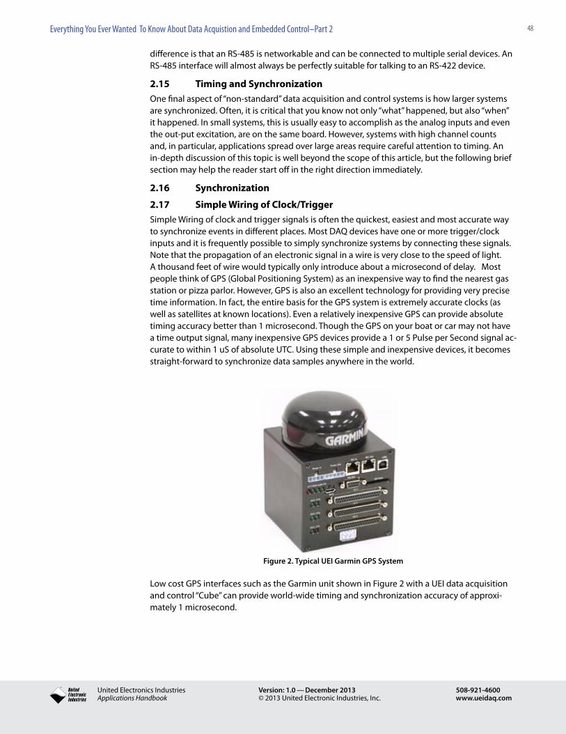
48Everything You Ever Wanted To Know About Data Acquistion and Embedded Control–Part 2
® United Electronics IndustriesApplications Handbook
Version: 1.0 — December 2013© 2013 United Electronic Industries, Inc.
508-921-4600www.ueidaq.com
difference is that an RS-485 is networkable and can be connected to multiple serial devices. An RS-485 interface will almost always be perfectly suitable for talking to an RS-422 device.
2.15 Timing and SynchronizationOne final aspect of “non-standard” data acquisition and control systems is how larger systems are synchronized. Often, it is critical that you know not only “what” happened, but also “when” it happened. In small systems, this is usually easy to accomplish as the analog inputs and even the out-put excitation, are on the same board. However, systems with high channel counts and, in particular, applications spread over large areas require careful attention to timing. An in-depth discussion of this topic is well beyond the scope of this article, but the following brief section may help the reader start off in the right direction immediately.
2.16 Synchronization
2.17 Simple Wiring of Clock/TriggerSimple Wiring of clock and trigger signals is often the quickest, easiest and most accurate way to synchronize events in different places. Most DAQ devices have one or more trigger/clock inputs and it is frequently possible to simply synchronize systems by connecting these signals. Note that the propagation of an electronic signal in a wire is very close to the speed of light. A thousand feet of wire would typically only introduce about a microsecond of delay. Most people think of GPS (Global Positioning System) as an inexpensive way to find the nearest gas station or pizza parlor. However, GPS is also an excellent technology for providing very precise time information. In fact, the entire basis for the GPS system is extremely accurate clocks (as well as satellites at known locations). Even a relatively inexpensive GPS can provide absolute timing accuracy better than 1 microsecond. Though the GPS on your boat or car may not have a time output signal, many inexpensive GPS devices provide a 1 or 5 Pulse per Second signal ac-curate to within 1 uS of absolute UTC. Using these simple and inexpensive devices, it becomes straight-forward to synchronize data samples anywhere in the world.
Figure 2. Typical UEI Garmin GPS System
Low cost GPS interfaces such as the Garmin unit shown in Figure 2 with a UEI data acquisition and control “Cube” can provide world-wide timing and synchronization accuracy of approxi-mately 1 microsecond.

49Everything You Ever Wanted To Know About Data Acquistion and Embedded Control–Part 2
® United Electronics IndustriesApplications Handbook
Version: 1.0 — December 2013© 2013 United Electronic Industries, Inc.
508-921-4600www.ueidaq.com
2.18 IRIGIRIG (Inter-Range Instrumentation Group) is not so much a timing technology as it is a timing protocol. However, most of the high accuracy timing and synchronization systems available to-day have standardized on one of the IRIG protocols. These high performance timing devices are generically referred to as IRIG interfaces. The underlying timing of an IRIG device can be based upon many things such as GPS, WWV synchronization, or a highly stable and accurate on-board clock. The key to using an IRIG device is simply to look at the device’s rated timing accuracy and verify that this will provide the synchronization accuracy your system requires
SummaryAs you can see, there is often much more to specifying a data acquisition and control system than simply selecting the appropriate A/D, D/A, and digital I/O devices. Hopefully, this arti-cle has provided a useful introduction to some of the more common “second tier” interfaces. Should you need further information on any of these items, it should be readily available a few key-clicks away on your favorite web-based search engine.

50
® United Electronics IndustriesApplications Handbook
Version: 1.0 — December 2013© 2013 United Electronic Industries, Inc.
508-921-4600www.ueidaq.com
Board Versus Box
3 Design Notes
Board Versus Box: The Age-Old DAQ DilemmaSince the beginning of PC-based data acquisition and control in the 1980s, one question has remained a constant consideration for all who would specify a new DAQ system. Is this applica-tion better served by an external I/O “box” connected to the PC via some communications link, or an internal “board” system plugged into a slot within the computer? If anything, this ques-tion has become more complicated as technology has progressed. Data transfer rates achiev-able with a variety of board and external box technologies.
Today, you have a wider – and better – choice of interfaces for your DAQ system than ever before. External box systems based on 100Base-T and Gigabit Ethernet (including LXI), USB, GPIB, CAN, RS-232/485, as well as a variety of proprietary interfaces, are available. On the plug-in board side of the coil are interfaces for PCI, PXI, PCI Express, Cardbus and ExpressCard. Even boards for the original IBM PC’s ISA bus are still available. To further complicate matters, hybrid systems like UEI’s popular RACKTangle™ series offer the advantages of an external box with the flexibility and reconfigurability of a board system.
Choosing what’s best for a given application is not an easy task. Some of the parameters used to compare interfaces are:
• Systemaccuracy,• I/Ocount,• DistancebetweenDAQsystemandsensors,• Systemportability,• Expandability,• Flexibility,• Overallcost,• Bandwidth(DAQspeed),• Expectedproductlife.
System AccuracyIn the early days of PC-based DAQ, the general rule of thumb was: If you want high accuracy, choose a box. If you want high speed measurements, you need a board solution. Of course, there always was a “gray” area in between that could be addressed by either type of system. Today, however, the gray area is much wider than before. Both pure board level products as well as hybrid devices (external chassis that allow the installation of I/O boards) are now avail-able with very high accuracies. This has been made possible by a variety of changes in technol-ogy, much of which has little to do with the measurement technology itself. While a detailed description of these changes is beyond the scope of this article, a few notes might be both informative as well as interesting from a historical perspective. Perhaps the three most signifi-cant technology shifts that allow boards to be used in high accuracy applications are:
1. Multi-layer printed circuit board technology with integral shielding was quite expen-sive in the 1980s. Today, 4 and 6 layer boards are the norm.
2. All the electronics in a PC have migrated to MOS technology. For those too young to have ever played with the LSTTL logic in the original PC, consider yourself lucky. LSTTL generated enormous switching transients. A scope connected to +5 V in a TTL system looked more like the output of a cardiac ward’s EKG machine. Compared to TTL, today’s systems look like the patient has “flat-lined”.
51Design Notes Board Versus Box
® United Electronics IndustriesApplications Handbook
Version: 1.0 — December 2013© 2013 United Electronic Industries, Inc.
508-921-4600www.ueidaq.com
3. In the 1980s, the DC/DC converters often operated at 30 to 50 kHz…right in the fre-quency band of interest in many systems. Today most DC/DCs operate at 500 kHz or more, well above the bandwidth of most DAQ systems.
Of course, measurement technology has changed as well, and the availability of high accuracy delta sigma converters make it possible to “integrate out” much of the high frequency noise produced inside a PC.
Sample and/or Update RateAs mentioned previously, in the early days of DAQ, high-speed applications were typically han-dled by board-level products. The internal buses, even though slow by today’s standards, were faster than the data transfer rates provided by any external communications link. Today, the story is somewhat different as only the highest speed applications are beyond the capability of USB, Gigabit Ethernet, or Firewire, which theoretically support data transfers of 62.5, 50 and 30 million 16-bit sample transfers per second respectively (although the theoretical limits are rarely achievable). The new internal board-level bus, PCIExpress, is based upon multiple very high speed (~ Gbps) serial paths. Though 2 Gbps is quite fast, the PCI Express spec does not stop there. PCI Express allows up to 16 of these serial links in each direction. The total possible data transfer rate of a full PCI Express implementation is 32 Gbps in each direction. This is fast enough for all but the highest digital scope “type” applications.
Interestingly, the very highest sample rates are once again provided by external box systems, but rather than transferring the data directly into a host computer, these systems transfer the data directly into high speed memory contained within the DAQ box itself. After the acquisition is complete, this data can then be downloaded to the host PC for subsequent display and analysis.
I/O Channel CountMost people assume that external box-type systems inherently allow for more expandability and may be a better choice for a large system than a plug-in board system. That is often true, especially considering most of today’s desktop and even tower PCs typically include only a few I/O slots. Also, more and more users are switching to laptop computers, which have extremely limited I/O support.
Distance Between Host Computer and SensorThis is an important consideration in many applications, more important than many people re-alize. It is important for two major reasons:First, running long multi-conductor cables between your test system and sensors can be very expensive, especially with a large system. Conversely, running a single, twisted-pair CAT5 communication cable, is relatively “cheap and easy”.
Second, each foot of wire connecting your sensor or output to a remote host computer increases your susceptibility to noise. Quiet measurements of 18-bits and greater are almost impossible to achieve when you have long connection wires. Mounting the DAQ system close to the signal source, however, significantly reduces this noise potential.
Portability of DAQ SystemSome systems need to be portable, of course. A wide variety of small, external box devices are available today that meet this need, which is a far better approach than dragging a desktop or tower PC around a test site. Don’t overlook PXI when portability is important, however, because several compact 4- and 6-slot PXI chassis are now available that can also meet this need.
Preferred Host ComputerLaptop computers are becoming more popular and their capabilities have expanded to the point where they are now suitable for almost any type of user. Your options for developing a plug-in board-based DAQ system around your laptop, however, are rather limited. Although

52Design Notes Board Versus Box
® United Electronics IndustriesApplications Handbook
Version: 1.0 — December 2013© 2013 United Electronic Industries, Inc.
508-921-4600www.ueidaq.com
many PCMCIA/PC-Card options, as well as a number of Compact Flash-based devices, are now available, their capabilities and expandability are severely limited. Most new laptops now come with Ethernet and USB ports, and many include Firewire as well. Portability Among Different Host Platforms External box systems certainly have the edge here. Even if your next PC is func-tionally identical to your existing computer, do you really want to remove all your I/O boards and install them in your new computer? Also, as technology changes, the number and types of slots inside computers change. If your current system has 4 PCI boards in it, are you sure your next PC will have homes for them? Of course, there is no guarantee your next computer will have the same external connections as your current PC, but the probability is almost certainly higher.
PriceThe “old” rule of thumb was that, all else being equal, a plug-in board-based system was likely to carry a smaller price tag. This is no longer the case today, however, as some of the lowest cost DAQ interfaces ever released now offer USB and/or Ethernet interfaces. Expected Product Life-With so many interfaces and system options available today, some of them will not survive for long. It is important, therefore, that you be aware of trends in the marketplace and not select a system type that is likely to become obsolete during the lifetime of your DAQ system. It is also smart to select an interface and system type that is growing in popularity rather than a time-worn design that may be good today but declining in market acceptance and, quite possibly, “end-of-lifed” and un-available tomorrow.
ConclusionBased upon the considerations we have described above, it is usually pretty clear which technology provides the best solution for a given application. Should this not be the case, the decision of which system to purchase may revert to the age-old standard of head to head com-petition among DAQ vendors. In such cases, the decision is often based upon which vendor will offer the best support. One final thing to consider is how much a particular vendor charges for support. Though many DAQ vendors offer their customers free phone/email based technical support, there are a few who do not. Often the price of support is enough to sway a decision one way or another.
This article was written by Bob Judd, Director of Sales and Marketing at United Electronic Industries (UEI) (Walpole, MA). For more information, contact Mr. Judd at [email protected]
53
® United Electronics IndustriesApplications Handbook
Version: 1.0 — December 2013© 2013 United Electronic Industries, Inc.
508-921-4600www.ueidaq.com
Design Notes A Modern Alternative to Reflective Memory and VME
A Modern Alternative to Reflective Memory and VMEThis white paper is divided into two sections. The first provides a brief description of some of the reasons our customers have switched from Reflective Memory and VME based technology to UEI’s Ethernet RACKtangle and Cube I/O chassis. The second part is a case study of the process as well as how and why FlightSafety International, a world leader in the design and manufacture of flight simulators, made the switch to UEI.
IntroductionReflective Memory, and in particular, Reflective Memory in VME chassis has been the standard for real-time DAQ and embedded control systems for years. However, due
to the age of most VME technology, as well as the recent consolidation of vendors in the mar-ket, many VME users have, or will soon face “end-of-life” issues with their VME solutions. Reflec-tive Memory itself is an older, proprietary technology and may itself be facing end-of-life in the not too distant future. In the meanwhile, new technology from UEI provides the functionality of Reflective Memory in a simpler, less expensive, and more modern architecture. With a 10+ year availability guarantee, UEI’s powerful RACKtangle I/O system is an ideal replacement for VME based I/O systems, whether or not they use Reflective Memory technology.
Reflective Memory HistoryDeveloped in the 1980’s and popularized for VME systems by VMIC, Reflective Memory is a method for sharing and synchronizing data in multiple chassis. Reflective Memory networks typically provide the deterministic timing required by real-time control systems and at the same time minimize the network load on the chassis CPU. In VME systems, Reflective Memory I/O systems are typically configured with an RM board in each chassis. These Reflective Memory boards are then connected via some type of communications link/network.
An “image” of the I/O is created in the I/O chassis that describes the state of all the I/O at a given instant in time. A duplicate, Reflective Memory image is created in the CPU chassis. A communi-cations link (typically fiber) is also provided connecting the two boards. The Reflective Memory system takes care of keeping the two memory images synchronized and identical in a time deterministic manor. This synchronization is done in the background automatically for the user.
When the CPU wants to query an input in I/O chassis, it need only read the appropriate memory location in the local RM board. Similarly, when the host CPU wants to write to an output in the I/O chassis, it needs only write to the appropriate memory location in the local RM board. The RM system ensures the I/O images are updated, that current input data is available in the local chassis and that the output data on the RM card in the CPU chassis is written to the RM board in the I/O chassis (which the I/O chassis is then responsible for writing to the appropriate I/O card.).
The BIG disadvantages with Reflective Memory are that it takes up a valuable slot in your VME chassis and more importantly, the boards are quite costly.
UEI’s Modern Alternative to Reflective MemoryUEI’s patented DMAPTM alternative to Reflective Memory provides the same functionality, but eliminates the requirement for dedicated memory boards by taking advantage of recent tech-nology and in particular, speed advances in CPU, FPGA, DDR2 memory technologies. DMAP uses a simpler, less expensive architecture and uses a standard Ethernet techology as the com-munications link. On the host side, instead of keeping the data image in a Reflective Memory board, the UEI system uses a section of the host CPU’s standard memory. On the I/O chassis side, as opposed to adding an expensive Reflective Memory board, UEI’s solution reads and writes the data from the various I/O boards’ actual data registers. This configuration eliminates the requirement for any special memory board as utilized in Reflective Memory systems.
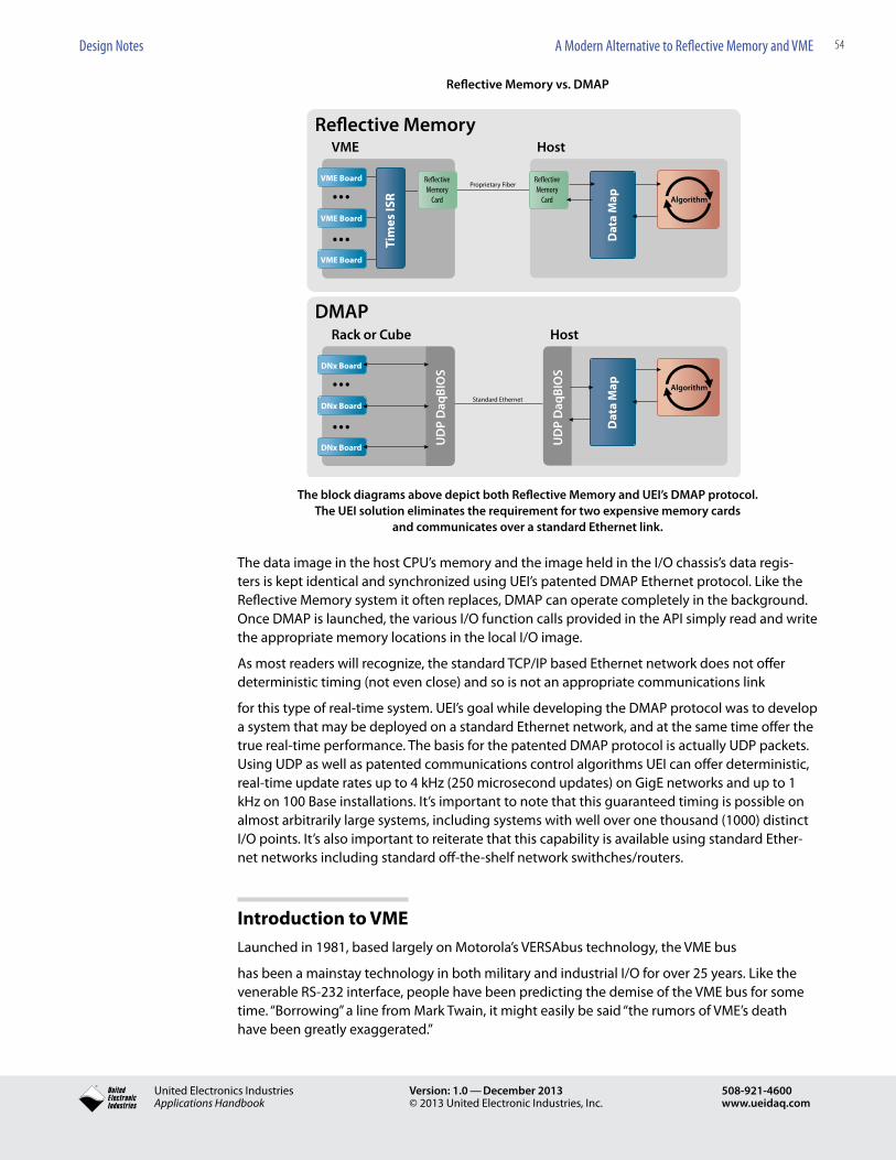
54Design Notes A Modern Alternative to Reflective Memory and VME
® United Electronics IndustriesApplications Handbook
Version: 1.0 — December 2013© 2013 United Electronic Industries, Inc.
508-921-4600www.ueidaq.com
Reflective Memory vs. DMAPRe�ective Memory vs. DMAP
Rack or Cube Host
VME Host
DMAP
Re�ective Memory
UD
P D
aqBI
OS
UD
P D
aqBI
OS...
...DNx Board
DNx Board
Dat
a M
ap
DNx Board
...
...VME Board
VME Board
Dat
a M
ap
VME Board
Algorithm
Algorithm
Tim
es IS
R
Re�ectiveMemoryCard
Re�ectiveMemoryCard
Standard Ethernet
Proprietary Fiber
The block diagrams above depict both Reflective Memory and UEI’s DMAP protocol. The UEI solution eliminates the requirement for two expensive memory cards
and communicates over a standard Ethernet link.
The data image in the host CPU’s memory and the image held in the I/O chassis’s data regis-ters is kept identical and synchronized using UEI’s patented DMAP Ethernet protocol. Like the Reflective Memory system it often replaces, DMAP can operate completely in the background. Once DMAP is launched, the various I/O function calls provided in the API simply read and write the appropriate memory locations in the local I/O image.
As most readers will recognize, the standard TCP/IP based Ethernet network does not offer deterministic timing (not even close) and so is not an appropriate communications link
for this type of real-time system. UEI’s goal while developing the DMAP protocol was to develop a system that may be deployed on a standard Ethernet network, and at the same time offer the true real-time performance. The basis for the patented DMAP protocol is actually UDP packets. Using UDP as well as patented communications control algorithms UEI can offer deterministic, real-time update rates up to 4 kHz (250 microsecond updates) on GigE networks and up to 1 kHz on 100 Base installations. It’s important to note that this guaranteed timing is possible on almost arbitrarily large systems, including systems with well over one thousand (1000) distinct I/O points. It’s also important to reiterate that this capability is available using standard Ether-net networks including standard off-the-shelf network swithches/routers.
Introduction to VMELaunched in 1981, based largely on Motorola’s VERSAbus technology, the VME bus
has been a mainstay technology in both military and industrial I/O for over 25 years. Like the venerable RS-232 interface, people have been predicting the demise of the VME bus for some time. “Borrowing” a line from Mark Twain, it might easily be said “the rumors of VME’s death have been greatly exaggerated.”

55Design Notes A Modern Alternative to Reflective Memory and VME
® United Electronics IndustriesApplications Handbook
Version: 1.0 — December 2013© 2013 United Electronic Industries, Inc.
508-921-4600www.ueidaq.com
However, time does march on. Though the VME bus has seen modernization including wider data buses (e.g. VME64) and additional instrumentation features (e.g. VXI), the reality is that VME is now seen as a “cash cow” market by many VME suppliers. In today’s marketplace, VME is simply not seen as deserving significant investment in new product develoment or maintenance.
The VME market has seen quite a bit of consolidation over the past few years, and it’s difficult for the new larger entities to justify manufacturing small quantities of boards from different groups all performing the same function. At the same time, many of the components that have been designed into these products are being discontinued by the semiconductor manufactur-ers due to ROHS and/or low volume. Finally, as more and more production is moving to the “East”, it is difficult to justify transferring the manufacturing fixtures and knowledge for many VME boards to off shore partners, particularly some of the relatively low volume analog and digital I/O boards.
The reality of product obsolescenceAll these factors have driven many vendors to discontinue a variety of their VME I/O boards. This regrettable trend (at least if your system is based on boards about to go “End-Of-Life” or EOL) is not likely to change at any time in the future. This leaves many VME users facing obsolete components and last-time buys. Even many VME users who have yet to face an EOL disturbance are certainly looking over their shoulder and wondering when their purchasing department will give them the bad news.
Faced with an EOL issue, a growing number of designers are looking for other alternatives. Though redesigns based upon substitute VME products are sometimes possible, it is not a popular option as there is no telling when the next VME board will bite the proverbial dust. More and more engineers are basing their replacement systems on modern COTS Ethernet I/O products, and computers.
The long-term solution is guaranteed*UEI’s Ethernet I/O products are only a few years old and are based upon up to date modern technology. In addition, UEI has an incredible track record for maintaining production of products and not forcing our customers to upgrade to the latest, greatest technology until they want to, not need to. This is a promise backed by our 10- Year Aailability Guarantee.
Other key reasons to switch to Ethernet I/OOnce backed into a corner and forced to consider non-VME solutions, designers are delighted to find a host of benefits and advantages a UEI I/O chassis provides over the VME chassis to which they have grown accustomed. Indeed, product obsolescence is often not the primary reason a VME designer switches to a UEI solution. Sometimes the designer simply needs a fea-ture or capability not available on a VME platform.
The following section describes the advantages and benefits the UEI Cubes and RACKtangles have relative to VME systems.
Small size / high channel densityThe UEI Cube and RACKTangle allow you to pack more I/O into a smaller space than VME racks. A DNA-PPC8 Cube measures just 4.0” by 4.1” by 5.8” and yet allows the installation of up to 150 A/D channels, 192 D/A channels, 288 DIO points, 72 ARINC 429 channels, 12 MIL-1553 ports, 48 Serial ports, 48 counter/timer/quadrature channels or 24 CAN-bus ports. The 12-slot RACKtan-gle I/O chassis provides double these quantities in a standard 3U rack form factor.
Using our high density chassis, designers have found they no longer need to mount their I/O in remote racks and then run long cables between the I/O rack and the main “product” (e.g. a simulator, a dynamometer, a test stand, etc.). Mounting the I/O right on the product decreases noise pick up in the signal wiring and reduces the cost and complexity of running hundreds

56Design Notes A Modern Alternative to Reflective Memory and VME
® United Electronics IndustriesApplications Handbook
Version: 1.0 — December 2013© 2013 United Electronic Industries, Inc.
508-921-4600www.ueidaq.com
and sometimes thousands of wires between the sensors and a remote I/O rack. With the I/O mounted locally, installing your product at a customer or final installation site is as simple as connecting power and Ethernet.
Customers who take advantage of the Programmable Automation Controller versions of UEI’s I/O also eliminate the space required by an external host computer. The UEIPAC builds a stand-ard Linux based (with Xenomai RTOS support) operating system directly into the I/O chassis, allowing the units to run full stand-alone.
FlexibilityFlexibility comes both from the unique Cube/RACKtangle form factor and from the extraordi-nary array of different I/O boards that may be installed in a UEI Ethernet Chassis. With I/O Cubes as small as 4” by 4.1” by 4”, you can put a UEI chassis in places you’d never dream of installing a VME rack. Our I/O Cube is rated from -40 °C to +85 °C, 50g shock, 5g vibration, 0-70,000 feet altitude and has been radiation tested for space applications. If that’s not enough, our fiber optic interface allows the I/O system to be mounted up to 20 kM from the host computer. That’s handy when the I/O is located on the ocean floor, 15,000 feet below the host PC mounted on an oil drilling platform.
For applications requiring the absolute smallest footprint and/or the ability to survive in the most rugged environments, UEI’s Cube is ideal. For more traditional, rack- based
applications, the RACKtangle is a perfect solution.
As for I/O flexibility, UEI offers over 30 different boards. In addition to stan- dard analog and digital I/O, there are CAN-bus, RS-232/422/485, ARINC-429, quadrature encoder inputs and soon there will even be a MIL-STD-1553 board.
Software SupportLike most I/O manufacturers, UEI offers incredible support for all popular Windows Develop-ment languages and applications. Unlike many I/O vendors, UEI also provides factory written drivers for all popular Linux and Real-Time operating systems including QNX, VXworks, RT Linux, Windows RTX, RTAI Linux and more.
PriceOur customers find that when they switch from VME to UEI technology, their system price goes down. If you add the cost savings provided by smaller rack sizes, shorter wiring, and the time saved by using our easy-to-use software drivers, the cost savings become even more significant.
PerformanceDoes Ethernet I/O offer the performance available on the VME platform? The answer is a re-sounding yes. Our patented DMAP Ethernet protocol ensures systems with thousands of I/O
57Design Notes A Modern Alternative to Reflective Memory and VME
® United Electronics IndustriesApplications Handbook
Version: 1.0 — December 2013© 2013 United Electronic Industries, Inc.
508-921-4600www.ueidaq.com
points are monitored and updated, all in less than a millisecond. As you’ll see in the case study included later in this paper, FlightSafety International monitors/updates their I/O points at 2 kHz.
COTS productionIf you’re building your first system, you don’t want to wait 6-12 weeks to get a piece of hardware to evaluate. If you’re releasing your project to produc- tion, you don’t want to hear from pur-chasing that the component you need is 12-16 weeks away. Finally, if your up and running and your system takes a lightning hit, you don’t want to find out a replacement board is two months away. All of UEI’s Cube and RACKtangle I/O products are standard, off-the- shelf products. Even in the unlikely event we are out of a product you need for an emergency replacement, we will scramble and find something we can get to you to get you back up and running immediately.
Case Study: FlightSafety InternationalPiloting an aircraft without training is an inherently dangerous endeavor. Though early aviation pioneers were forced to take this risk or stay on the ground, this is no longer the case. Almost all pilots start their training in single engine, piston powered aircraft accompanied by a flight instructor. Most advanced training, and in particular, training of professional pilots in turbine powered aircraft, is now performed in a simulator.
Flight simulators offer a number of key advantages over training in actual aircraft. First and fore-most is safety. It’s possible to simulate almost any emer- gency or system failure in a simulator without risking life or limb. The same is certainly not true in an actual aircraft. It’s perfectly safe for a student pilot to experience an engine failure on takeoff in a simulator. If the student is slow to abort the takeoff and the simulator runs off the runway, no damage is done (except to egos).
Another key advantage of flight simulator training is the cost savings of simulated flight versus actual. Though simulators are not inexpensive, it’s still much less expensive for a pilot to take his/her “check ride” in a simulator than actually firing up and flying a Boeing, Airbus or other aircraft.
Though there were earlier attempts to build a ground based flight simulator, most consider the Link trainer developed by Edwin Link in 1929 to be the first “real” simulator. Following a number of US Army Air Corps accidents in the early 1930s, the army purchased four of Link’s simulators and the flight simulator industry was born.
FlightSafety International was founded in 1951, dedicated to the principle that aviation safety is best achieved through training. With a fleet of nearly 400 simulators, FlightSafety is the world’s leading supplier of flight simulators. Since the beginning, they have been a leader in develop-ing simulator tech- nology. For simulator training to be economically viable, simulators must:
1. Accurately replicate the “look and feel” of the actual aircraft
2. Provide an extraordinary level of reliability as most simulators are “flown” around the clock and are scheduled out weeks, if not months, in advance.
3. Allow quick repair. Simulators are complex devices and all devices can fail. It is critical to be able to diagnose and repair any failures quickly.
4. Be maintainable. A simulator is an expensive piece of capital equipment. To justify the investment, the simulator must have a long life, and so, must be assembled from components that will be available for many years.
5. Use standardized, well established components so new simulators, and in particular, simulators of new aircraft are developed in a timely manner with a minimum of new “learning curves” to be climbed.
6. Offer attractive pricing. Simulation is a competitive market. In order to prosper, a simulator must be able to offer competitive prices.

58Design Notes A Modern Alternative to Reflective Memory and VME
® United Electronics IndustriesApplications Handbook
Version: 1.0 — December 2013© 2013 United Electronic Industries, Inc.
508-921-4600www.ueidaq.com
FlightSafety’s new SimI/O equipped simulators have been developed to meet all of the above requirements and more. Though FlightSafety’s current simula- tors are the highest perfor-mance, most technologically advanced simulators available, the new SimI/O equipped simula-tors serve to further distance them from the competition.
The high density of the RACKtangle allows it to be mounted in cabinets at the base of the simulator (above) or in racks within the simulator (right) rather than in “off-sim” racks.
In their development of the new series, FlightSafety investigated a host of different I/O vendors and systems. In the end, the company has standardized all computer based I/O (including flight deck I/O, control loading and motion, and avionics) on the United Electronic Industries (UEI) RACKtangle I/O chassis and its associated I/O boards.
The remainder of this paper will detail how UEI’s RACKtangle chassis is lever- aged to achieve these goals in the new SimI/O equipped simulators. We will break the discussion down into distinct advantages though you will notice there is frequently an overlap where a particular RACKtangle I/O chassis fea- ture has a positive influence on more than one system issue.
High performance:Performance is always an issue on a simulator. Obviously the goal is to make the simulator per-form EXACTLY like the real aircraft. The new RACKtangle I/O equipped simulators have helped FlightSafety enhance the performance of the SimI/O equipped simulators in a number of ways.
1. The RACKTangle to computer interface is implemented via 1000base-T, Gigabit Ethernet. The Gigabit implementation ensures communication between inputs, the controlling computer and control/display output is fast and does not become a gating issue. Also, the ability to address 12 I/O boards in a single rack, with a single IP address reduces the overhead required to “talk” to the I/O system. The 12-slot rack provides up to 300 analog input, 384 analog output, 696 digital I/O or 144 ARINC-429 chan- nels. The high Gigabit data transfer rate, combined with the low over- head, enables system scan/update rates of 2000 Hz. This enhances overall system “smoothness” and allows control algorithms to make smaller, more accurate changes and adjustments.
59Design Notes A Modern Alternative to Reflective Memory and VME
® United Electronics IndustriesApplications Handbook
Version: 1.0 — December 2013© 2013 United Electronic Industries, Inc.
508-921-4600www.ueidaq.com
2. Ensuring there are no “hiccups” or uncommanded “bumps” in the simula- tor requires the use of a computer with an operating system offering de- terministic timing. There is no time to stop the control system algorithms while a disk drive is written or a monitor updated. SimI/O equipped simulators utilize the Ardence RTX® – Real-time Extension for Control of Windows operating system. UEI’s RACKtangle chassis includes complete support for the RTX real time operating system (RTOS) as well as most other popular RTOS including QNX, VXworks, RT Linux, and RTAI Linux. Though many I/O manufacturers have ignored the Linux/RTOS market or relegated the support to unof-ficial user forums, UEI drivers are factory written and fully supported.
3. On SimI/O equipped simulators, the I/O chassis are mounted directly on the simulator itself as opposed to previous designs where the actual I/O interfaces where mounted in racks external to the simulator. The on- board location of the SimI/O allows shorter wiring lengths, which decreas- es noise pickup and increases the system’s overall signal to noise ratio.
High reliabilityWhether the simulator is operated by an airline, a government agency, or a training division of FlightSafety unscheduled simulator down time is a disas- ter. Not only does it reduce billable/us-able hours, it creates schedule chaos. Most simulators are operated “round the clock” and it is ex-tremely difficult, if not impossible, to “make up” time lost by a down simulator. In particular, pilots of Part 121 airlines have extremely tight schedules, and their training sched- ules are not flexible. A pilot who misses a check ride because the Sim is down is effectively grounded. This not only causes hardship for the pilot, but also the airline, which is then forced to allocate a reserve pilot as a replacement. FlightSafety’s simulators offer a remarkable 99.6% availability. Assuming the simulator is scheduled out 24/7, this represents less than three hours of down time per month. Two key factors determine simulator availability. These are reliability (typically expressed as mean time between failures or MTBF) and epairability (often referred to as mean time to repair or MTTR). The new RACKtangle I/O solution enhances both MTBF and MTTR. We will discuss the reliability advancements here while repairability topics will be covered in the next section.
The new UEI based simulators are designed to improve on FlightSafety’s already extraordinary reliability. Here’s how:
59. Historically, simulators have been installed in two “parts”; the actual simulator and the external control station. All I/O connections had to be wired directly from the sim to the control panel. In complex aircraft, this requires a wiring harness containing over one thousand wires. The fact that the simulators move in 6 degrees of motion greatly complicates this connection and requires the use of a “waterfall” wiring scheme. The high I/O density of the UEI RACKtangle I/O chassis has allowed FlightSafety
to build the entire control station into the simulator itself. The waterfall wiring harness on a SimI/O equipped simulator now contains little more than power and Ethernet connections. All I/O wiring is fixed in place. The elimination of thousands of moving wires greatly reduces the probability of a broken wire or connector causing a system failure.
2. Today’s aircraft cockpits are filled with annunciator lights and indicators. Turn them on at the same time and the cockpit takes on the look of a Christmas tree. Though there is a movement toward the use of high reli- ability LED indicators, the bulk of the indicators in most aircraft remain incandescent bulbs. Incandescent bulbs left on (or off ) are extremely reli- able and will last for years. There are reports of a bulb installed at a Texas opera house that has been burning constantly since September of 1908! However, the thermal shock, and corresponding rapid ex-pansion/contrac- tion of bulb filaments as they are turned on/off dramatically reduces bulb life. The Guardian series digital output modules installed in the UEI RACK- tangle provide a pulse width modulated (PWM) “soft-start” capability.
60Design Notes A Modern Alternative to Reflective Memory and VME
® United Electronics IndustriesApplications Handbook
Version: 1.0 — December 2013© 2013 United Electronic Industries, Inc.
508-921-4600www.ueidaq.com
The soft-start allows the bulb filament to be brought up to temperature (and brightness) gradually enough so thermal shock is greatly reduced, yet quickly enough that there is no no-ticeable impact on the display. This feature dramatically improves bulb life and reduces down time. (Note the PWM feature can be set to run at steady state duty cycles. This allows the digital outputs to also serve as a “virtual rheostat” and allows the outputs to offer a “dimmer” capability in addition to simply turning bulbs on or off.)
Rapid diagnosis and repairsFlightSafety simulators are remarkably reliable. However, failures in a device as complex as a simulator are inevitable. A critical design goal of the SimI/O equipped simulators is to reduce the mean time to repair once a system or component has failed. UEI’s RACKtangle I/O chassis has allowed FlightSafety to reduce the amount of time required for the repair technician to di-agnose problems. It has also enabled the technicians to make many repairs more quickly. Many failures are now diagnosed and repaired in the amount of time it takes the crew to grab a cup of coffee. In fact, many failures can be fully diagnosed while the sim is still running! Also, the simpler and faster repairs made possible by the new SimI/O diagnostics allow the simulation operator to maintain a smaller, less technically advanced repair and maintenance staff.
Here’s how the RACKtangle I/O chassis helps accomplish these goals.
1. Each RACKtangle I/O chassis provides two Ethernet connections, at independent IP addresses. One of the IP addresses is used by the simula- tor host computers to read and write the I/O. The second is available as a diagnostics “snoop in” port and diag-nostics software may be run while the simulator is actually operational. Many, if not most, simulator failures do not bring the simulator “down”, but merely make certain procedures or functions unavailable. It is often possible for the instructor to move on to a different part of the training syllabus with a “failed” system on board. The ability to run diagnostics concurrently with actual training will make it possible for the repair technician to identify the cause of a failure, de- termine which component(s) need replacement, acquire the components from stock, and prepare to perform the repair without stopping the train- ing. Of course it’s unlikely the repair can be made while the Sim is operat- ing. However, since the technician knows exactly what to replace, how to replace it, and has the items in hand before bringing the sim down, the repairs are often made in minutes, not hours.
2. All SimI/O inputs are connected to an internal switch that allows the input to be dis-connected from the live SimI/O and connected to a predefined test signal. Similarly, all SimI/O outputs can be independently moni- tored. The ability to fully test all I/O automatically dramatically simplifies and speeds up diagnosing any problems identi-fied in the cockpit or via system generated error alarms. This capability also allows complete self- tests and identifies wiring and installation problems without requiring manual wiring and continuity testing. A key aspect of the self diagnostics is the ability for the RACKtangle’s digital outputs to monitor their actual output voltage and cur-rent, while the digital inputs are able to monitor not only hi and low, but to actually measure the input voltage with 25 mV accuracy. This measurement capability makes it possible not only to detect failures, but also to note changes in system behavior that might be predictive of pending failures.
3. The new Ethernet based “diagnostic IP” system enables a standard wire- less interface to the technician’s remote, hand-held diagnostic unit. In ad-dition to identifying the problem, the system also provides instant access to any required schematics, user manuals, and/or wiring diagrams.
4. The second diagnostic IP address also supports a Web browser interface allowing a senior technician or engineer to access the system remotely. They can then diagnose
61Design Notes A Modern Alternative to Reflective Memory and VME
® United Electronics IndustriesApplications Handbook
Version: 1.0 — December 2013© 2013 United Electronic Industries, Inc.
508-921-4600www.ueidaq.com
and correct any issues beyond the local techni- cian’s capability without requiring any travel or travel related down-time.
5. The modular nature of the RACKtangle, combined with the ability to re- place any I/O module in a matter of seconds, greatly reduces repair time. The RACKtangle chassis contains no active components. All I/O modules, the CPU/NIC module and power supply modules are all easily replaced. The new SimI/O system is based upon a small number of standard COTS components, reducing the on-site requirement for spares as well as en- suring fast access to replacement components when necessary.
6. Not all simulator features and functions are used in all training sessions. SimI/O’s self test and diagnostic capabilities allow the system to self test between sessions. The engine fire, cabin depressurization, or alternator failure warning annunciators might be used infrequently, but must work when commanded. The self-test features allow these components to be automatically checked. Should a failure be noted, it is pos-sible for the technician to correct the situation between sessions, during scheduled maintenance, or while another repair is made without causing any down- time and without impacting training efficacy.
Extended simulator lifeThough efficient and cost effective, there is no debate that a flight simulator is an expensive piece of capital equipment. As such, a purchaser/operator of a flight simulator needs to know the device will be viable far into the future. UEI’s RACKtangle I/O series was the perfect choice as the basis for the I/O requirements in the new Sim I/O equipped simulators. Here’s why.
1. Previous versions of FlightSafety’s flight simulators have been based upon VME tech-nology. Though many vendors remain committed to supporting the VME bus, many others, and in particular those focusing on I/O prod- ucts are moving on to other platforms (e.g. Ethernet, LXI, etc.). To ensure long term availability of the hardware required to build new simulators as well as to support those already in the field, it was necessary to switch to a more stable architecture. (Note: FlightSafety has taken the necessary steps to ensure there will not be any disruption in support for existing simulators. Also, if required, it will be possible to retrofit existing simulators with Sim I/O hardware.)
2. The Ethernet in its various formats is ubiquitous and has been supported in one form or another since 1980. The Gigabit Ethernet interface cur- rently used in UEI’s RACK-tangle I/O system is becoming well established in the I/O control environment and will provide a stable communications protocol for many years to come.
3. UEI and FlightSafety are partners in the Sim I/O endeavor. Previous simu- lators have been based upon I/O systems provided by a large number of different vendors. Though FlightSafety’s I/O purchases were significant, they have not always been large enough to justify a vendor’s continued production of a given component. This is particularly the case as more and more of the VME based components have been “EOL-end of lifed”. In the Sim I/O case, all I/O will be purchased from UEI. The partner-ship ensures a continued supply of product, now and in the future.
4. UEI serves a large number of OEM customers who depend on the company to provide a long-tem, uninterrupted supply of measurement and control products. UEI’s com-mitment is demonstrated daily by the compa- ny’s willingness to continue supplying its OEM customers ISA bus boards developed almost 20 years ago. UEI product sup-port has even gone so far as to clone and provide a stable source of I/O boards that have been discontinued by other vendors. UEI is a vendor committed to long term support of its products and its OEM customers.
62Design Notes A Modern Alternative to Reflective Memory and VME
® United Electronics IndustriesApplications Handbook
Version: 1.0 — December 2013© 2013 United Electronic Industries, Inc.
508-921-4600www.ueidaq.com
Timely development of new simulatorsPrevious simulators have been based on I/O supplied by a variety of vendors. Though this situation was workable, it was not optimal. It mandated develop- ers to use multiple, often dramatically different, software and hardware form factors. In the SimI/O equipped series, all I/O hardware and software, includ- ing avionics instrument control (AIC), control loading and motion (CLM) and flight deck I/O (FDK) is based upon the UEI RACKtangle I/O series. Here’s how the UEI RACKtangle helps FSI get their new simulators up and running quickly.
1. In the new SimI/O architecture, all I/O is based on the UEI RACKtangle I/O chassis.This chassis allows great flexibility as any of the 25+ available I/O modules may be installed in any of the rack’s 12 I/O slots. The standard form factor and footprint allow FlightSafety to standardize on the I/O and control bay on each simulator and yet have an almost limitless ability to configure the I/O to match the particular aircraft. The RACKtangle pro- vides unprecedented I/O density, including up to 300 analog input, 384 analog output, 144 ARINC-429 channels per rack.
2. The software interface to all of the I/O capability is provided in a single, straightforward API. This dramatically reduces the time required by the software developers to actu-ally write the application programs. It provides portability so application code may be shared among different development groups. It dramatically simplifies software docu-mentation and maintenance as all the I/O is based upon a single driver. Finally, when a driver software update is required, it is achieved by updating a single driver.
Lower cost:Though performance, availability, and supportability are the key issues that drove FlightSafety to standardize on the UEI RACKtangle series, the UEI sys- tem also provides all of its advantages and reduces the cost of SimI/O based systems relative to previous configurations. The UEI based system reduces overall cost in a number of ways.
1. The UEI RACKtangle I/O costs less than the previous VME based systems.
2. The advanced diagnostics provided dramatically reduce debugging of a newly built simulator. This reduces the time and labor costs required to get a new simulator up and running.
3. Reduced cost of construction due to the reduction in waterfall wiring required. This offers dramatic cost savings both in “parts” cost and in as- sembly labor. This is of particular note as almost all simulators are built twice. Once at the factory to prove proper operation, and then again at the simulator’s final location, be it a FligthSafety or customer facility.
4. The actual size of “on-simulator” equipment cabinet is reduced by over 50%. This reduces the cost of the structure required to support the I/O system.
5. Common I/O and chassis components reduce the requirement for on-site spare prod-ucts. The spares requirement is also reduced as all of the RACK- tangle components used in the SimI/O equipped sims are standard COTS products at UEI and there are no long delivery schedules that need to be considered when it comes to planning the stock of spare components.
63Design Notes Real-Time Extensions for Linux
® United Electronics IndustriesApplications Handbook
Version: 1.0 — December 2013© 2013 United Electronic Industries, Inc.
508-921-4600www.ueidaq.com
Real-Time Extensions for LinuxIn order for Linux to be a true alternative to traditional real-time operating systems, its lack of determinism must be dealt with. Real-time extensions have recently made this an easy problem to solve.
While market analysts and others focusing on the business side of computers have become aware of the growing importance of Linux, a secondary market exists with potentially just as much impact: real-time extensions for Linux. Indeed, engineers designing embedded systems have come to embrace Linux as a genuine alternative to more traditional real-time operating systems. This two-part series examines what’s involved in working with real-time Linux and is based on the experiences of someone who has devoted the past year to writing data-acquisi-tion drivers that run under that environment.
A Bit of HistoryMore than a decade ago, I was developing software for an ultrasound scanner. Back then, in the era of the 80286, MS-DOS was almost the only OS suitable for embedded PC development. It offered everything we needed, as well as being clear and straightforward to work with. Indeed, the only limits designers faced came from the PC hardware. Even today, DOS executes any in-terrupt immediately, and nothing can interrupt the code. The program’s timing was sufficiently precise, and all system functions adapted well enough to use on an embedded platform.
At that time, real-time systems were quite simple and typically included one main loop, as shown in Listing 1. This simplicity, however, also brought along a few problems. Unavailable were the OS services we take for granted today, such as networking, database accesses, file-system operations, graphics, and running the user interface. Writing any of those services from scratch, as well as supporting them for at least a couple devices, requires enormous engineer-ing effort. In addition, systems were totally unscaleable, and managers accepted their use only because of the high cost of an off-the-shelf PC at the time. Despite these drawbacks, PC-based systems addressed the main requirement of a hard real-time system: guaranteed timing dead-lines that the system can’t miss under any circumstances.
while (alive)
{
get_sensor_data(); // read one or more sensors
compute_control(); // calculate control parameters based on
// incoming data
control_device(); // initiate control activity
// read next group of sensors...calculate...control
}Listing 1: Main loop
Then Windows came along to ease the burden on the user who didn’t want to work at the command line. However, its new structure and scheduling mechanism added a large degree of uncertainty as to when a given program might run. Thus, in response to the needs of embed-ded programmers, the number of dedicated real-time OSes mushroomed. Many of them grew from the simple main-loop concept, but they unfortunately inherited the limitations of their ancestors. Other full-service RTOSes are well-crafted and thoroughly thought out, but to this day they remain somewhat limited with regard to what applications and tools are available to developers. Certainly, one of these single-source solutions could, at times, prove advantageous
64Design Notes Real-Time Extensions for Linux
® United Electronics IndustriesApplications Handbook
Version: 1.0 — December 2013© 2013 United Electronic Industries, Inc.
508-921-4600www.ueidaq.com
for completing a project, but in many cases you must write a significant part of the project’s individual components yourself without the support of large developer community.
In contrast, working with a general-purpose OS significantly reduces development and deploy-ment costs as well as time to market. You can draw from a wide variety of off-the-shelf tools, services, example programs, and complete applications. This situation is especially true for a Unix-like OS, and open-source options such as Linux have proven especially attractive. Indeed, many established vendors of real-time software are migrating rapidly toward embedded Linux, examples being QNX and Lynx Real-Time Systems; Lynx even went as far as changing its name to LynuxWorks. In addition, newer players, such as RedHat, MontaVista, TimeSys, and Lineo provide tools and OS code for embedded real-time applications. Finally, even the establishment is giving credibility to the movement as IBM, HP, Motorola, and 3Com have aligned themselves behind the growing Embedded Linux Consortium.
Meanwhile, it’s now possible to shrink an image of embedded Linux to fit within low-end targets as small as 4KB (according to Michael Tiemann, chief technology officer at RedHat). In addition, Linus Torvalds, who wrote the original Linux code but who is now working with mo-bile-processor maker Transmeta, is adding power management and a compressed file system to embedded Linux to help make it even more suitable for battery-powered mobile systems where programs must squeeze into a tiny footprint. These changes make Linux an increasingly appealing choice for designers selecting an embedded OS. [1] [2]
Real-Time Linux ArchitectureNow consider the technical reasons behind the growth of real-time enhancements for Linux. The key fact is this: design decisions that are brilliant for a general-purpose OS are lethal for a real-time one.
A general-purpose OS can’t operate in real time because its designers must achieve good performance for multiple applications running at the same time-but without performance optimized for any particular one of them. Further, major OS advances such as virtual memory, large caches, hardware-request reordering, and optimization hinder, rather than help, with real-time performance. For multiprocess systems minimizing context-switching time is important. And while coarse-grained schedulers move towards that goal, they make it more difficult, if not impossible, to run a time-critical process on time.
Let’s look at OS developments from the opposite perspective. One way to improve real-time performance is to add extra preemption points where the OS can stop execution of one pro-cess and give time to a critical one. However, this approach decreases overall performance in a multiprocessing system; designers tune general-purpose OSes for best overall average perfor-mance, making worst-case behavior non-deterministic.
The solution to the problem comes with an understanding of the dissimilar nature of these two major classes of operating environments. By decoupling the real-time part of an OS from the general-purpose kernel, it’s possible to optimize the real-time part separately to meet timing deadlines while allowing the rest of the system to show the best-possible performance. This approach is exactly what the creators of RTLinux (www.rtlinux.org) and RTAI (www.rtai.org) did when they developed their real-time extensions. Both of these products are available at no cost under a general public license, meaning open source and free. Although these two implemen-tations of real-time Linux differ somewhat (see sidebar, “Subtle differences in real-time imple-mentations: elegance vs. practicality”), they both operate in a similar fashion. For consistency, the examples in this article use the RTLinux API.

65Design Notes Real-Time Extensions for Linux
® United Electronics IndustriesApplications Handbook
Version: 1.0 — December 2013© 2013 United Electronic Industries, Inc.
508-921-4600www.ueidaq.com
Subtle differences in real-time implementations: elegance vs. practicalityProfessor Paolo Mantegazza started the RTAI project based on Victor Yodaiken’s RTLinux v. 1. Since then, RTLinux and RTAI have gone through long development paths on their own. Despite the fact that they’re not API-compatible, their functionalities are very similar. All key primitives and services exist in both packages. Both offer:
• Asmallreal-timecore• One-shotandperiodictimersupport• Real-timescheduler• Real-timethreads• Real-timeFIFOsandsharedmemory• Real-timeinterrupthandler
In my opinion, RTAI provides a more practical API while RTLinux is more elegant. On the other hand, RTAI is more elegant in how it integrates into the Linux kernel. The RTAI team makes a constant effort to add features that people ask for, and thus its API has grown to become reasonably extensive. For example, RTAI includes clock (8254 and APIC) calibration, dynamic memory management for realtime tasks, LXRT (Linux Extension for Real Time) to bring soft/hard real-time capabilities into user space, remote procedure calls, and mailboxes.
The RTLinux team aims to keep their real-time Linux extensions as predictable as possible, add-ing only features that won’t hurt designs and compatibility in the future. In short, the RTLinux API is more consistent, but many practitioners prefer to use RTAI. Thanks to ongoing competi-tion, almost everything you can accomplish in one package you can do in the other. This same competition also encourages dramatic improvements in both products. The latest versions, RTLinux 3.0 and RTAI 1.6/24.1.3, are excellent mature products, and their authors have done everything possible to smooth out the learning curve.
It’s fair to say that VenturCom’s RTX and Radisys’ (now TenAsys) INtime for Windows NT are also based on the concept of splitting real-time and nonreal-time tasks, and they do show excellent results. However, they are closed-source and relatively expensive in terms of tools and royalties.
In both cases, the real-time kernel inserts a very thin layer-perhaps just a hundred lines of code-between the interrupt-control hardware and the Linux kernel (Figure 1). When Linux issues a request to enable or disable an interrupt, the real-time kernel sees the request first and thus controls all interrupt vectors from the start. Instead of dealing with actual interrupt-control hardware, however, the real-time kernel writes the request into an internal data structure and returns control to Linux.
Thus Linux is completely isolated from the interrupt-control hardware. Instead, the real-time kernel emulates that hardware with a virtual machine layer. Now any incoming interrupt first invokes a routine in the real-time kernel, which checks whether a real-time handler is registered for this interrupt. If it finds one, it passes control to that handler. If no handler is registered or if it shares this incoming interrupt with the Linux kernel, the real-time kernel invokes nonreal-time Linux handlers that can also use system resources.
The advantage of this approach is that Linux becomes the lowest priority task for the real-time kernel. You can think of the real-time Linux kernel as a small real-time OS that can suspend Linux’s execution at any state. It doesn’t care what Linux is doing the moment an interrupt ar-rives; it immediately switches context and passes control to a real-time task.
The core of real-time Linux is very thin-it contains only a hundred or so lines of code-because it handles only interrupt processing. Furthermore, that kernel doesn’t share any system resources with Linux. It doesn’t require dynamic memory allocation, a file system, or spin locks to access any data structure. That’s why it needn’t wait for Linux, but instead Linux waits for all higher pri-
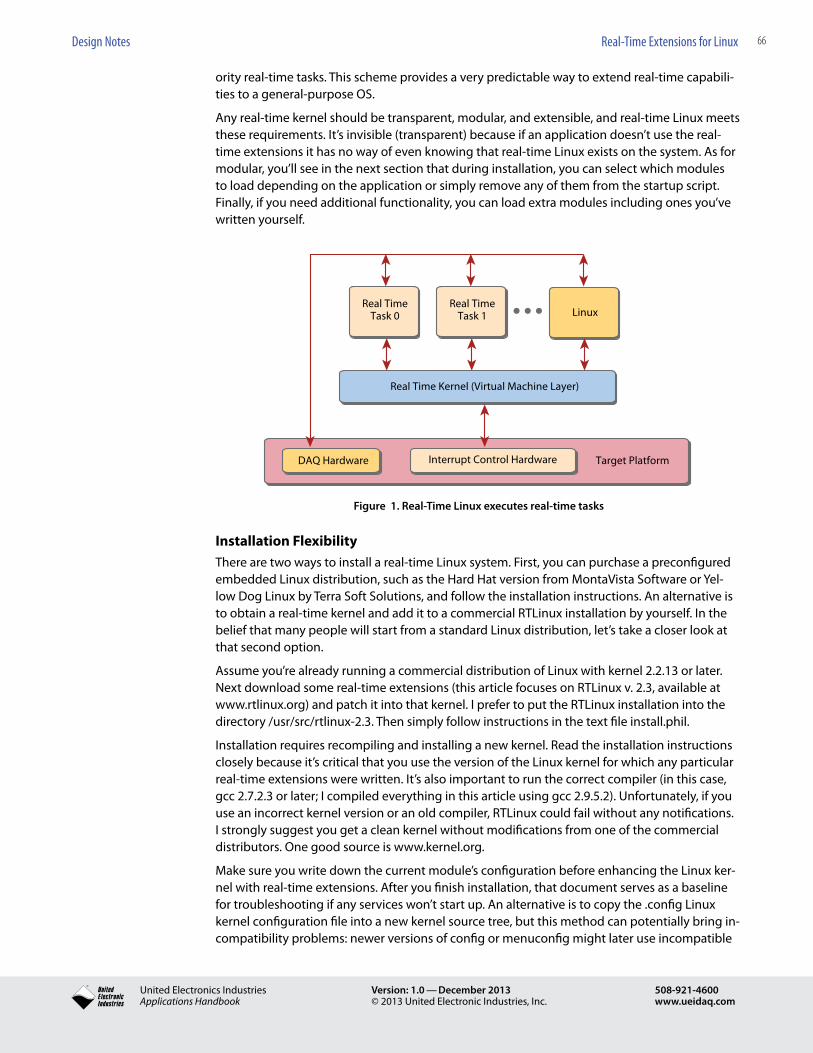
66Design Notes Real-Time Extensions for Linux
® United Electronics IndustriesApplications Handbook
Version: 1.0 — December 2013© 2013 United Electronic Industries, Inc.
508-921-4600www.ueidaq.com
ority real-time tasks. This scheme provides a very predictable way to extend real-time capabili-ties to a general-purpose OS.
Any real-time kernel should be transparent, modular, and extensible, and real-time Linux meets these requirements. It’s invisible (transparent) because if an application doesn’t use the real-time extensions it has no way of even knowing that real-time Linux exists on the system. As for modular, you’ll see in the next section that during installation, you can select which modules to load depending on the application or simply remove any of them from the startup script. Finally, if you need additional functionality, you can load extra modules including ones you’ve written yourself.
Real Time Kernel (Virtual Machine Layer)
Real Time Kernel (Virtual Machine Layer)
Real TimeTask 0
Real TimeTask 1 Linux
DAQ Hardware Interrupt Control Hardware Target Platform
Figure 1. Real-Time Linux executes real-time tasks
Installation FlexibilityThere are two ways to install a real-time Linux system. First, you can purchase a preconfigured embedded Linux distribution, such as the Hard Hat version from MontaVista Software or Yel-low Dog Linux by Terra Soft Solutions, and follow the installation instructions. An alternative is to obtain a real-time kernel and add it to a commercial RTLinux installation by yourself. In the belief that many people will start from a standard Linux distribution, let’s take a closer look at that second option.
Assume you’re already running a commercial distribution of Linux with kernel 2.2.13 or later. Next download some real-time extensions (this article focuses on RTLinux v. 2.3, available at www.rtlinux.org) and patch it into that kernel. I prefer to put the RTLinux installation into the directory /usr/src/rtlinux-2.3. Then simply follow instructions in the text file install.phil.
Installation requires recompiling and installing a new kernel. Read the installation instructions closely because it’s critical that you use the version of the Linux kernel for which any particular real-time extensions were written. It’s also important to run the correct compiler (in this case, gcc 2.7.2.3 or later; I compiled everything in this article using gcc 2.9.5.2). Unfortunately, if you use an incorrect kernel version or an old compiler, RTLinux could fail without any notifications. I strongly suggest you get a clean kernel without modifications from one of the commercial distributors. One good source is www.kernel.org.
Make sure you write down the current module’s configuration before enhancing the Linux ker-nel with real-time extensions. After you finish installation, that document serves as a baseline for troubleshooting if any services won’t start up. An alternative is to copy the .config Linux kernel configuration file into a new kernel source tree, but this method can potentially bring in-compatibility problems: newer versions of config or menuconfig might later use incompatible
67Design Notes Real-Time Extensions for Linux
® United Electronics IndustriesApplications Handbook
Version: 1.0 — December 2013© 2013 United Electronic Industries, Inc.
508-921-4600www.ueidaq.com
formats for the .config file. Whether you use the command make config or make menuconfig to set up the new configuration, it’s important to enable the following options in the Linux kernel configuration file: symmetric multiprocessing support, hard real-time support (in processor type and features), and loadable module support.
Don’t delete the old kernel from the /boot directory, and keep its respective record in lilo.conf. If something goes wrong during installation you can always press while booting and switch to the old kernel. Now compile the OS and install the RTLinux modules.
After installing the real-time extensions and recompiling any required modules, it’s a good idea to verify that everything went as expected. You can, for instance, try to run code from the /ex-amples directory. Those programs automatically call the instrtl script to load RTLinux modules. Later, if you don’t need real-time support, you can run the rmrtl script, which removes modules from the Linux kernel.
As we’ve just discussed, real-time Linux features a modular design that allows you to load only desirable portions of its functionality into the kernel space memory. This modularity makes it easier to fit real-time Linux in an embedded platform with tight memory requirements.
You have the choice of five primary and three additional RTLinux modules when deciding which to load into the kernel:
• rtl_time.o–controlsprocessorclocks• rtl_sched.o–implementsareal-timescheduler• rtl_posixio.o–providesaPOSIX-likeinterfacetodevicedrivers• rtl_fifo.o–createsareal-timenon-blockingFIFOimplementationbetweenreal-
time modules and user-space processes• mbuff.o–providesasharedmemorybetweenreal-timetasksanduser-space
processes• rtl_ipc.o–providesPOSIX-styleblockingmutexesandsemaphores• rtl_debug.o–addssupportforasource-leveldebugger• rtl_com.o–interfacewithserialports
For most real-time tasks, only the first four modules are necessary. Note that RTAI provides simi-lar modules but with different names.
Build Your First Real-Time ModuleLet’s now try to write, compile, and run a simple RTLinux application. This example implements a hard real-time periodic task that toggles the state of Line 0 on a PC’s parallel port 1,000 times a second.
Before doing any coding, be certain to understand that a RTLinux task itself is a kernel module. You load this task module only after you’ve loaded the RTLinux modules. In this way, the loader can now link functions in your task module to entry points in the real-time Linux modules. Fur-ther, because it’s a kernel module, your task should have at least two predefined entry points: intinit_module(void)andintcleanup_module(void).
Also assuming for the moment that the task code is already written, take a quick look at how easy it is to compile into the RTLinux task module, which you then load into the real-time ker-nel. One method is to quickly write a makefile script that creates the module, which here we’ve namedpp_flip.o(Listing2).

68Design Notes Real-Time Extensions for Linux
® United Electronics IndustriesApplications Handbook
Version: 1.0 — December 2013© 2013 United Electronic Industries, Inc.
508-921-4600www.ueidaq.com
# Makefile.pp_flip
all: pp_flip.o
RTLINUX = /usr/src/linux # the path to the rt-linux kernel
INCLUDE = ${RTLINUX}/include
CFLAGS = -O2 -Wall
pp_flip.o: pp_flip.c
gcc -I${INCLUDE} -I/usr/include/rtlinux ${CFLAGS} -D__KERNEL__ -D__RT__
- DMODULE -c pp_flip.c
clean:
rm -f pp_flip.oListing 2: makefile.pp_flip
That procedure isn’t really difficult, but there’s an even easier way to compile an RTLinux mod-ule, especially if it’s written all in C. During the RTLinux installation process, the makefile script for the initial step automatically generates a file known as rtl.mk, which contains all the re-quired compiler options and paths for a specific installation of RTLinux. Now all you need do is find that file, copy it into the directory with the source file for the real-time task, and type make -frtl.mkpp_flip.o.
Nowlet’smoveontothesourcecodeforthetaskinpp_flip.c.Startwiththerequiredheaders(inListing3)andnotethatbyincludingrtl_sched.hyouautomaticallyincludertl_conf.h,rtl_core.h,andrtl_time.h.ThesefilesdefinefunctionsfromseveralvitalRTLinuxmodulesincludingrtl_timeandrtl_sched.
#include
#include
#include
#include
#include
#include
#define LPT1_DATA 0x378 // parallel port 1 data
#define FRQ 1000 // thread period in Hz...
#define FRAME_PERIOD_NS ((hrtime_t)((1.0/FRQ) * 1000000000.0)) // ...and in ns
Listing 3: Includes and defines for pp_flip.c
Nextwritetheinit_module()entrypoint(Listing4),whichthemodutilsprogramcallswhenitinsertsthatmoduleintothekernel.Later,whenitactuallyruns,init_module()initializesthreadattributesandpreparesschedulerparameters.Andalthoughsched_get_priority_max(policy)doesn’t use the Policy argument in the current RTLinux release, I recommend that you set it to

69Design Notes Real-Time Extensions for Linux
® United Electronics IndustriesApplications Handbook
Version: 1.0 — December 2013© 2013 United Electronic Industries, Inc.
508-921-4600www.ueidaq.com
SCHED_FIFOforcompatibilitywithfutureversions.
pthread_t pp_thread;
// our periodic thread
void *pp_thread_ep(void *rate) {
static int nState = 0;
// make this realtime thread periodic
pthread_make_periodic_np(pthread_self(),gethrtime(),FRAME_PERIOD_NS);
// this loop wakes up once per period
while (1)
{
if (nState) outb(nStateý, LPT1_DATA); else outb(nState++,LPT1_DATA);
// wait until next period of time
pthread_wait_np();
}
}
int init_module(void) {
pthread_attr_t attrib;
struct sched_param sched_param;
// output string to /var/log/kern.log
printk(ýinit_module pp_flip\ný);
// prepare periodic thread for creation
// initialize thread attributes
sched_param.sched_priority = sched_get_priority_max(SCHED_FIFO);
// obtain highest priority
pthread_attr_init(&attrib);
// set our priority
pthread_attr_setschedparam(&attrib, &sched_param);
// and finally create the thread
pthread_create(&pp_thread, &attrib, pp_thread_ep, (void *)0);
return 0;
}
int cleanup_module(void) {
printk(ýcleanup_module pp_flip\ný);
pthread_delete_np(pp_thread); // kill the thread
return 0;
}
70Design Notes Real-Time Extensions for Linux
® United Electronics IndustriesApplications Handbook
Version: 1.0 — December 2013© 2013 United Electronic Industries, Inc.
508-921-4600www.ueidaq.com
Listing 4: pp_flip.c
When do you really need hard real-time performance?The difference between hard and soft real-time is that hard real-time performance always guar-antees exact timing. Two major groups of application need hard real-time:
• Closed-loopcontrolsystems(get-calc-puttype)• Stimulus/responsesystems(put-calc-gettype)
Good examples are robotics, animatronics, industrial equipment, digital models of analog systems, neural, fuzzy, adaptive systems, medical/biological test equipment, test-rig control and monitoring, and real-time simulation with hardware in the loop. If your application doesn’t fall into one of these categories, don’t bother with RTLinux. Adding the real-time environment might degrade the overall performance of the OS, make mouse response jerky, and make the keyboard unresponsive.
Atthispointthecodecallsawell-knownPOSIX-stylefunctionnamedpthread_create(),whichis part of the RTLinux API. The first parameter in that call holds a pointer to the real-time task’s thread structure; the second parameter gives thread attributes; the third defines the thread function; and the fourth is the thread argument. With that last argument you can pass any 32-bit value or pointer (to a structure). This example doesn’t use that parameter, but you could, for example, specify the frequency that way.
Thefunctioncleanup_module()hastheoppositepurpose.Thekernelcallsthatfunctionwhenitwantstounloadanymodule.Inthisexample,itkillsthereal-timetask’sthreadthatinit_mod-ule()created.Pleasenotethe_npsuffixinsomeofthefunctionsinListing4,forexample,pthread_delete_np().Thissuffiximplies“non-portable”or“non-POSIX”andmeansthatapar-ticular function is proprietary to RTLinux.
Theheartofourexample’smoduleispp_thread_ep(),theactualthreadfunction.RTLinuxcallsitalmostimmediatelyaftermakingthepthread_create()call.TheOSexecutesthatfunctionaslongas the thread is alive or until execution reaches the return statement. At the very beginning of the threadfunctionyoushouldcallpthread_make_periodic_np()totelltheRTLinuxschedulerthatyou want to make this thread periodic and execute it at exact time intervals. The first parameter is apointertothethread(inthiscaseweusepthread_self()togetit),thesecondoneisthestarttime(here, immediately), and the third parameter is the value of the period in nanoseconds.
Uponmakingthepthread_make_periodic_np()call,RTLinuxmarksthethreadasperiodicandready for execution. The RTLinux scheduler starts thread execution at the designated start time and runs it until it passes the period interval. If you set the period to 0 the thread executes only once. Otherwise it continues to run in an infinite loop. First it flips Line 0 on LPT1 and then calls pthread_wait_np().ThisfunctionhandsoversystemcontrolfromthethreadtoRTLinuxsched-uler, which hands control back to the thread at the start of the next period.
It’s time to test the program. You’ll start with two utilities from the modutils package. Specifi-cally, insmod loads a module into the running Linux kernel and resolves symbolic links; rmmod removes a module from the kernel and cleans up symbolic links.3 During all insmod/rmmod operations make sure you’re logged in as the root or become a super-user.
Now connect an oscilloscope to Pin 0 of LPT1 (see sidebar, “Tracking timing and worst cases”). Compilethereal-timemodulewiththecommandlinemake-fmakefile.pp_flipandinsertitintoarunningRTLinuxkernelwiththecommandinsmodpp_flip.o.Youshouldseeamessagefromtheinit_module()routine,andtheOSalsologsthatmessageintoafileat/var/log/kern.log.Fi-

71Design Notes Real-Time Extensions for Linux
® United Electronics IndustriesApplications Handbook
Version: 1.0 — December 2013© 2013 United Electronic Industries, Inc.
508-921-4600www.ueidaq.com
nally,tostopexecutionofthereal-timemodule,issuethecommandrmmodpp_flip.Thekernelcallsthecleanup_module()entrypointbeforeitremovesthemodulefromkernelmemory.
Tracking timing and worst casesWhen writing real-time code, you should design algorithms to ensure their deterministic behavior. Don’t use recursions or heuristic algorithms without worst-case limiters. Never cre-ate blocking calls in a real-time task. There are several ways of tracking timing and worst case performance.Oneistocallrt_get_time(),whichreturnstimeinticks.Flushtheresultofthisfunction into one of the realtime FIFOs, then read and store the stream in user space, for exam-ple cat /dev/rtf0 > ticks.dat. Then write a small script to analyze this file for the time difference between ticks.
Another way to analyze the performance of the example program from this series of articles is to attach a scope with a deep memory to the parallel-port pin. Switch the scope into enve-lopemodewiththemaximumnumberofsamplesavailable.Add#defineLP_PORT0×378intoyour program, and each time you get into an important place of your realtime task, flip one or anotherbitoftheparallelportwithacommandsimilartooutb(value,LP_PORT);.Theshapeofthe signal on the scope display clearly shows jitter and latency variations.
To find a worst-case condition you could also attach a logic analyzer to the same parallel port and set up logical conditions to trigger when delay between strobes exceeds a predefined value.
At this time it’s prudent to heed a warning that strongly advises you against using a method of checking program execution that’s common among many programmers. Specifically, it’s not safe to call printk() from RTLinux threads or handlers. Instead use the RTLinux-safe log function rtl_printf()towritemessagesintothesyslogfile.
Talking With The HardwareBesides the real-time operating system, another key component of a data-acquisition system is the device driver that controls the digitizing hardware. This discussion assumes that you’re working with a data-acq card that sits on either the PCI or PXI bus and includes a FIFO to buffer analog I/O operations. It also assumes that you already have a device driver for that board writ-ten to run under a commercial Linux distribution. (Consult the references list at the end of this article for more on non real-time Linux device drivers.)
With this driver loaded, the real-time module should be able to communicate directly with the data-acq hardware. However, it’s generally wise to split a complex real-time task by using sepa-rate instances of the data-acquisition device driver for real-time and non-real-time tasks. You can write, debug, and test pieces of data-acq code in the user space and only afterwards port them into the real-time environment.
Another issue to consider is how the driver should interface to a calling program. When insmod inserts a module into a running Linux kernel, it resolves the symbolic name of that module’s entry points into pointers to the module’s functions. It also inserts all symbolic names marked as“export”intothesymboltable.Forexample,afteryouloadthertl_fifo.omodule,allexportedfunctions within it become available to other modules.
Real-time Linux tasks and the Linux kernel run in the same address space. And if your data-acq driver exports needed entry points, the real-time module can use them. Of course, be sure to insert the data-acq driver into the Linux kernel before doing the same for the real-time module.
This approach has pros and cons. If a real-time module calls driver functions directly, it’s difficult to avoid synchronization issues or guarantee that a second task won’t call the same board in
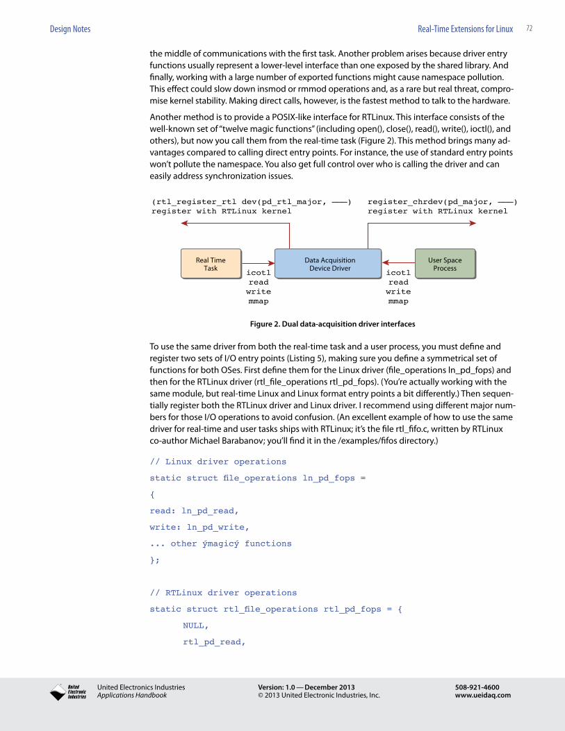
72Design Notes Real-Time Extensions for Linux
® United Electronics IndustriesApplications Handbook
Version: 1.0 — December 2013© 2013 United Electronic Industries, Inc.
508-921-4600www.ueidaq.com
the middle of communications with the first task. Another problem arises because driver entry functions usually represent a lower-level interface than one exposed by the shared library. And finally, working with a large number of exported functions might cause namespace pollution. This effect could slow down insmod or rmmod operations and, as a rare but real threat, compro-mise kernel stability. Making direct calls, however, is the fastest method to talk to the hardware.
Another method is to provide a POSIX-like interface for RTLinux. This interface consists of the well-known set of “twelve magic functions” (including open(), close(), read(), write(), ioctl(), and others), but now you call them from the real-time task (Figure 2). This method brings many ad-vantages compared to calling direct entry points. For instance, the use of standard entry points won’t pollute the namespace. You also get full control over who is calling the driver and can easily address synchronization issues.
Data AcquisitionDevice Driver
User SpaceProcess
Real TimeTask
(rtl_register_rtl dev(pd_rtl_major, –––)register with RTLinux kernel
icotlreadwritemmap
icotlreadwritemmap
register_chrdev(pd_major, –––)register with RTLinux kernel
Figure 2. Dual data-acquisition driver interfaces
To use the same driver from both the real-time task and a user process, you must define and register two sets of I/O entry points (Listing 5), making sure you define a symmetrical set of functionsforbothOSes.FirstdefinethemfortheLinuxdriver(file_operationsln_pd_fops)andthenfortheRTLinuxdriver(rtl_file_operationsrtl_pd_fops).(You’reactuallyworkingwiththesame module, but real-time Linux and Linux format entry points a bit differently.) Then sequen-tially register both the RTLinux driver and Linux driver. I recommend using different major num-bers for those I/O operations to avoid confusion. (An excellent example of how to use the same driverforreal-timeandusertasksshipswithRTLinux;it’sthefilertl_fifo.c,writtenbyRTLinuxco-author Michael Barabanov; you’ll find it in the /examples/fifos directory.)
// Linux driver operations
static struct file_operations ln_pd_fops =
{
read: ln_pd_read,
write: ln_pd_write,
... other ýmagicý functions
};
// RTLinux driver operations
static struct rtl_file_operations rtl_pd_fops = {
NULL,
rtl_pd_read,

73Design Notes Real-Time Extensions for Linux
® United Electronics IndustriesApplications Handbook
Version: 1.0 — December 2013© 2013 United Electronic Industries, Inc.
508-921-4600www.ueidaq.com
rtl_pd_write,
... other ýmagicý functions
};
// register Linux driver...
if (register_chrdev(PD_LN_MAJOR, ýpdaqý, &ln_pd_fops))
{ handle errors... }
// ...and RTLinux driver
if (rtl_register_chrdev(PD_RT_MAJOR, ýpdaqý, &rtl_pd_fops))
{ handle errors... }
Listing 5: Registering a driver for use by real-time and non real-time tasks
The downside of this approach is that it takes extra programming effort. Fortunately, you can cut down on this effort by creating an OS Abstraction Level (OSAL), as in Figure 3. Here you iso-late the hardware-specific part of the driver from the OS-specific portion. Instead of calling the OS directly, all calls to the driver come through the OSAL, whether the driver needs to talk to hardware or make some system calls. For example, if the driver must copy a portion of memory toreturnresults,itcallstheOSALfunctionosal_memcpy().Ifareal-timetaskmadethedrivercall, OSAL in turn calls memcpy(). If the call originated from the user space, OSAL instead calls thecopy_to_user()function.
OS Abstraction Layer
• Initialization and Cleanup• Common Part of I/O Entry Points• Parameter Checking• Memory Alloc/free• Messages/signals
Data Acquisition Hardware-Speci�c Code
• Initialization• Function Calls• Interrupt-processing Routines• Dispatch Routines (For ioctl/read/write)• Buffering/event Processing
Linux Kernel-Speci�c Calls Interface
• Memory Access• User Space Access• I/o Entry Points• Debug Messages• Signals
RTLinux-Speci�c Calls Interface
• Memory Access• I/o Entry Points• Debug Messages• Irq Request/release• Messages
Figure 3. OSAL driver design allows you to run the same driver for user-space and real-time tasks
Note that the I/O entry points are different for a real-time task and a user-space process. An OS-specific interface performs the initial processing of an I/O request and then calls the main I/O dispatch routine (Listing 6). The common part of the read() entry point doesn’t use anything specific to RTLinux or any other OS. The common part of each POSIXIO entry point is a separate function.
// read entry point registered by rtl_register_rtldev()
74Design Notes Real-Time Extensions for Linux
® United Electronics IndustriesApplications Handbook
Version: 1.0 — December 2013© 2013 United Electronic Industries, Inc.
508-921-4600www.ueidaq.com
static ssize_t rtl_pd_read(struct rtl_file *filp, char *buf,
size_t count, loff_t* ppos)
{
u32 minor = RTL_MINOR_FROM_FILEPTR(filp);
board = minor / PD_MINOR_RANGE;
subsystem = minor % PD_MINOR_RANGE;
return pd_read(minor, buf, count);
}
// read entry point registered by register_chrdev()
static ssize_t ln_pd_read(struct file *filp, char *buf,
size_t len, loff_t* ppos)
{
u32 minor = MINOR(inode->i_rdev);
return pd_read(minor, buf, count);
}
// main read() function
int pd_read(u32 minor, char *inpbuf, size_t count)
{
u32 board = minor / PD_MINOR_RANGE;
u32 subsystem = minor % PD_MINOR_RANGE;
// process read request to particular board and subsystem
...
}
Listing 6: Driver’s RTLinux and Linux entry points for read()
Before starting to write a device driver, you must decide whether it’s necessary to support real-time and user-space calls at the same time. For most embedded applications you need either one or the other and thus can simplify the overall design with a conditional compilation. For example,Listing7showstheosal_memcpy32()functionjustdiscussed.Ifyoumustcompilethedriverforusefromareal-timetask,simplydefine_NO_USERSPACEandrecompilethedriver.Otherwise it copies data into the user space.
unsigned long osal_memcpy32(u32* to, u32* from, u32 len)
{
#ifdef _NO_USERSPACE
return (u32)memcpy(to, from, len);
#else
return copy_from_user(to, from, len);

75Design Notes Real-Time Extensions for Linux
® United Electronics IndustriesApplications Handbook
Version: 1.0 — December 2013© 2013 United Electronic Industries, Inc.
508-921-4600www.ueidaq.com
#endif
}
Listing 7: Different calls for usertkernel spaces
76Design Notes Real-Time Extensions for Linux
® United Electronics IndustriesApplications Handbook
Version: 1.0 — December 2013© 2013 United Electronic Industries, Inc.
508-921-4600www.ueidaq.com
On some occasions, though, you might want to be able to communicate with the same driver from both a user process and a real-time task. For example, an application might require two data-acq boards of different types that share the same driver in one system; the user app runs one card, and the real-time task controls the second card. Obviously, such a driver must support calls from both tasks at the same time. The easiest way to achieve this goal is to mark the origi-nation of any I/O requests and process them with respect to the caller. However, be very careful to avoid race conditions.
If you’re writing a device driver instead of working with one that ships with the data-acq hard-ware, it’s also important to realize that a real-time Linux driver must follow more strict limita-tions then a Linux driver. For instance, when a real-time task makes a call, the driver shouldn’t do any of the following:
• Allocateorfreememory• Useprintk()orsimilarI/Oroutines• Makeblockingcalls• CopydatatoorfromtheuserspaceorsomehowinvoketheVMM(virtual
memory manager)• Usespinlocksorothersynchronizationobjectsbetweenreal-timecodeand
Linux kernelObviously, the behavior of a real-time driver should be deterministic. Recall that real-time Linux treats the Linux kernel as the lowest priority task. When your real-time task receives control, Linux itself can be in an unpredictable state such as in the middle of a spinlock or interrupt handler. Thus, you can’t rely on Linux services.It’s a good practice to put everything the driver might have to deal with-memory allocation and other mentioned services-into the routines init_module()andcleanup_module().Trytoavoidperformingtheseunsafeoperationsinsidethe real-time task.
If you have a shared library that allows access to the driver from the user space, you can use the same library to make calls from a real-time task. The best way to write the library is with condi-tional compilation, based on which space the library must support.
Registering InterruptsAnother topic of interest to real-time programmers is interrupt processing. It’s commonly known that a PCI board can generate only one host interrupt. Thus you can’t tell immediately what caused an interrupt, especially when several boards share the same line. Additionally, both a driver serving real-time Linux as well as a second one serving standard Linux might both have to process a given interrupt. For example, a program using a multifunction I/O board might require real-time response to an interrupt caused by digital I/O or a counter timer along with non-real-time streaming of analog input data to a disk file.
These two seemingly contradictory requirements lead to the following solution. The driver for standard Linux registers itself for the interrupt first, and then the real-time Linux driver registers itself for that same line. When an interrupt arrives, the real-time task processes it and controls digital I/O lines. Then the real-time Linux calls the interrupt handler registered by the Linux driver to perform the rest of the processing, which consists of things difficult or unwise to run under the real-time portion of the OS, such as feeding a new page list into a bus-mastering unit or copying data into a user buffer.
Floating-Point SupportA final issue concerns the fact that complex digital control systems usually require some floating-point operations. However, most operating systems, including Windows, don’t sup-port the use of a floating-point unit (FPU) in kernel drivers. The main reason is to avoid wasting

77Design Notes How to Design Linux Device Drivers for Data-Acquisition Boards—Part 1
® United Electronics IndustriesApplications Handbook
Version: 1.0 — December 2013© 2013 United Electronic Industries, Inc.
508-921-4600www.ueidaq.com
How to Design Linux Device Drivers for Data-Acquisition Boards Part 1Roll up your sleeves and learn how to design device drivers for data-acquisition boards.
Linux is now an attractive alternative to Windows, especially among engineers who roll up their sleeves and type at the command line. Linux offers a stability you just can’t get with Windows 95/98 or even Windows 2000. As a result, the demand for Linux systems and compatible periph-erals is mushrooming.
Because you’ll find little measurement hardware with support software for Linux, you may decide to write your own Linux drivers. Writing drivers for Linux is no trivial task, and this article presents some tips that could make your work go more smoothly. This article describes driver registration, naming, and access, as well as hardware initialization.
If you’re new to Linux programming, you’ll find a dearth of resources for programmers and developers, both in print and online. Reference 1 gives you an overview of how Linux device drivers work. You’ll also find few development and debugging tools for Linux. Nonetheless, you can implement some basic debugging tricks.
If you’ve previously worked with Unix, you should feel at home with Linux. But take note of a few key differences. For instance, the Unix and Linux kernels have different function names, implementation details, and levels of sophistication.
Ground RulesAsyoureadthelistingsinthisarticle,you’llseefunctioncalls,thatareprecededwithpd__.Youneed to use different calls, but these give you ideas for how you can construct your own driver. This article assumes that you know how to write C code that writes data to and reads data from an I/O port. The driver architecture described here works as well for multiple cards as it does for a single card, making for easy upgrading and expandability. Any card you use must have a FIFO buffer to store readings, a feature standard on virtually all modern PCI data-acquisition cards.
Figure 1.Drivers for data-acquisition boards reside in kernel space. You can control a driver either through read() and write() commands or through functions calls using the ioctl() command.
vRegardless of the target hardware, you should write your drivers in two parts. The first consists of low-level code that allows the driver to communicate with the target card at the register level. The second consists of the interface between the driver and the OS. Low-level register

78Design Notes How to Design Linux Device Drivers for Data-Acquisition Boards—Part 1
® United Electronics IndustriesApplications Handbook
Version: 1.0 — December 2013© 2013 United Electronic Industries, Inc.
508-921-4600www.ueidaq.com
code differs for every I/O board. Instead, This article examines the portion of the driver that communicates with the operating system.
Device drivers typically reside in the kernel space of the OS (Figure 1) because code in the user space, which is memory-protected by Linux, has no direct access to hardware. In this way, the OS protects itself from errant applications. Because a driver resides in the kernel space and can work directly with hardware, it can create havoc—even a system crash—elsewhere if you write data to a wrong address. So, be sure to write your code carefully.
Crucial Questions• Beforeyoucancreateadata-acquisitiondevicedriverforLinux,youmustanswer
several questions:• Doyouwantapplicationprogrammerstohaveaccesstoallofthedata-acquisi-
tion board’s hardware options?• Whatminimumlevelofsystemperformancewillthedriverrequire?• Doyouwantshellaccess(fromtheLinuxprompt)tothedriveroraccessthrough
function calls only?• Shouldyoukeepthedriversimpleoraddthecomplexitythatmakesitportable
across operating systems?
When you decide whether all of a data-acquisition card’s I/O subsystems—analog input, analog output, digital input, digital output, and counter/timers—should support concurrent access by different processes, carefully consider the costs and benefits. Access from multiple processes is difficult to implement and is often unnecessary.
Figure 2. Design a driver in two parts. Keep the hardware- and OS-dependent portions separate, so you can use the driver with another board or another OS without writing an entirely new driver.
When you design a Linux driver, you have two choices of driver: block and character. Block drivers can process data in an arbitrary order, but they function similarly to a disk drive. These drivers are best suited for devices that can have a file system.
Data-acquisition devices always need a character driver, whose read/write operations have access to data only in sequential order. Don’t let the “character” name mislead you: A character
79Design Notes How to Design Linux Device Drivers for Data-Acquisition Boards—Part 1
® United Electronics IndustriesApplications Handbook
Version: 1.0 — December 2013© 2013 United Electronic Industries, Inc.
508-921-4600www.ueidaq.com
driver also can work with blocks of data if one of the arguments you pass to is a pointer to a block of data.
Now, consider how to set up the user and application interfaces for your driver (Figure 2). Linux gives you access to device drivers as if they were files. Linux users are accustomed to controlling a driver through shell commands and scripts. Therefore, your driver should include a minimal set of functions accessible using read() and write() operations at the Linux shell command.
Although read() and write() shell commands also let application programmers call the driver directly from their programs, you can provide access to the driver in another way: by creating a library that encapsulates your application-programming-interface (API) calls. Using libraries shields application programmers from making calls directly to the low-level code that controls a card’s registers.
When the driver needs to inform the test application about a hardware event, such as a buffer half-full condition, it sends a signal to the library, which in turn calls a call-back function into the application. A library can also allocate buffers in system memory and connect them to the driver, so this approach hides system-dependent details from the applications and makes driv-ers portable across operating systems.
Linux device drivers exist as files in a directory called /dev. When you create a driver file, you register the device’s name with the OS. As part of the registration process, Linux identifies driv-ers by integers. Each driver has one major number and can have several minor numbers. It’s easy to view installed drivers along with their major numbers by going to the OS shell, moving to the /dev directory, and executing the ls –l command. This command lists all special files, a class into which device drivers fall.
Driver-Naming ConventionsOne driver can serve all devices of similar functionality coming from one manufacturer. So, you typically assign a major number to each group of related drivers. Each minor number refers to a specific subsystem—such as analog input—on a specific board. For example, you could employ the script in Listing 1 to tell the OS which major and minor numbers to associate with a particu-lar device driver. The person installing a card runs this script, which the hardware manufacturer supplies as part of a device-driver kit, during board installation.
$max_cards = 2;
$major = 61;
$minor_range = 5;
system(“rm -f $base_dir/daq-*”);
for ($card = 0; $card < $max_cards; $card ++)
{
print “daq card $card\n”;
$minor = $card * $minor_range;
system(“mknod $base_dir/daq-c$card-ain c $major $minor”);$minor ++;
system(“mknod $base_dir/daq-c$card-aout c $major $minor”);$minor ++;
system(“mknod $base_dir/daq-c$card-dio c $major $minor”);$minor ++;
system(“mknod $base_dir/daq-c$card-uct c $major $minor”);$minor
80Design Notes How to Design Linux Device Drivers for Data-Acquisition Boards—Part 1
® United Electronics IndustriesApplications Handbook
Version: 1.0 — December 2013© 2013 United Electronic Industries, Inc.
508-921-4600www.ueidaq.com
++;
system(“mknod $base_dir/daq-c$card-drv c $major $minor”);
system(“chmod 0666 $base_dir/daq-*”);
}
Listing 1: Driver-architecture specs
The first line in Listing 1 indicates how many cards this driver supports: two in this case. A driver architecture that supports any number of boards that contain any or all of the data-acquisition board’s subsystems makes it easy to add support for new generations of devices without re-writing major portions of the driver.
The second line in the script assigns to the group of cards a major number: 61. You can arbitrari-ly select a major number, but be aware that the OS reserves a few of them for specific purposes. Refer to a Linux programming book for details.
The script also tells the OS to define five minor numbers for each card, a number that equals the number of subsystems on the card. The next line is optional and makes a call to the OS to remove all device files with similar names to those the script is about to use. Now, for each of the two data-acquisition cards, the script uses the mknod (make node) command to create five de-vice files with these names: daq-cN-ain, daq-cN-aout, daq-cN-dio, daq-cN-uct, and daq-cN-drv.
Finally, the last line uses a series of octal numbers (here all sixes) along with the chmod com-mand to set the access rights to all device drivers that fall into the designated wild-card name; this line dictates that everybody has read/write permissions for the driver.
Try to use descriptive filenames for device drivers. For instance, the file /dev/daq-c0-ain gives the user access to the analog-input subsystem of card 0. This card is assigned minor numbers 0 to 4, whereas the analog-input subsystem of card 1 uses minor numbers 5 to 9. Drivers with different major numbers, however, can use the same set of minor numbers.
To avoid confusion with this numbering scheme, you can determine which board and subsys-tem an application program will open with a given driver. Insert the following lines of code in the driver:
board = minor /minor_range;
subsystem = minor %
minor_range;
The first line finds the integer value. The second uses the remainder to point to the minor number.
The OS cares about major numbers only; the driver keeps track of opening and closing minor numbers. You can minimize the driver’s complexity if you deny subsystem sharing. Write your driver so that it opens a minor number and stores the process ID (PID) of the process that opened it. If another process tries to gain access to the same minor number (board subsystem), the driver denies it access.
If, instead, the driver code lets several processes have access to the same board subsystem, the driver would have to stop any ongoing operation, store status values, reconfigure the board for another process, run the new operation, and then reset the board to its previous sta-tus. This sequence might not present difficulties if two applications with low throughput, such as a voltmeter and a thermocouple monitor, need to share a subsystem. But if one applica-

81Design Notes How to Design Linux Device Drivers for Data-Acquisition Boards—Part 1
® United Electronics IndustriesApplications Handbook
Version: 1.0 — December 2013© 2013 United Electronic Industries, Inc.
508-921-4600www.ueidaq.com
tion involves high throughput rates, such as a digital scope, sharing degrades an application program’s performance.
As part of your driver design, you should decide whether you want to grant access to your driver from the Linux command line. Providing such access lets application programmers and system integrators confirm that their hardware is working before compiling and running any code. If you’re familiar with Linux shell programming, you can use a driver directly from the command line using the Linux shell commands.
You might first want to open a driver by issuing a read() command using a typical name, such as /dev/daq-c0-drv. You receive information about Board 0, such as its serial number and the device’s current status. I suggest that you provide limited access to the driver through the Linux shell. Provide just enough access to let board installers test the board before they write applica-tion programs.
You can use read() and write() commands for simple devices. When dealing with a complex device that incorporates many functions, however, implementing reads and writes with a com-mand language can become confusing for users, and the driver must take steps to properly parse the command line. So, although these two commands are useful for accessing driver functions from the Linux shell, you should use the ioctl() command when you access the driver using an application program.
The ioctl() command presents a different entry point into the same driver code. Programmers working with Windows 95/98/NT are accustomed to using an ioctl() interface to drivers. Further, instead of requiring application programmers to include every I/O and driver parameter in the calling function, programmers can now use a pointer to a buffer that contains that information.
The structure of an ioctl() call is:
ioctl(unsigned int fd,
unsigned int request,
unsigned long argument)
The variable fd refers to a file descriptor that the application re-ceives when it opens the driver. Later, user code opens the device-driver file and then issues ioctl() calls to it. Through the request argument, you can specify the desired action, and the argument is a 32-bit variable that can be a pointer to a buffer containing I/O pa-rameters.
//============ ioctl dispatch routine ===================
static int pd_ioctl(
struct inode *inode,
struct file *file,
unsigned int command,
unsigned long argument
) {
int real_minor, board, board_minor, iRes;
// calculate board# and subsystem

82Design Notes How to Design Linux Device Drivers for Data-Acquisition Boards—Part 1
® United Electronics IndustriesApplications Handbook
Version: 1.0 — December 2013© 2013 United Electronic Industries, Inc.
508-921-4600www.ueidaq.com
real_minor = MINOR(file->f_dentry->d_inode->i_rdev);
board = real_minor / PD_MINOR_RANGE;
board_minor = real_minor % PD_MINOR_RANGE;
// check if this process owns the subsystem
if (!pd_CheckOwnerPID(board, board_minor, current->pid))
return -EBUSY;
// dispatch the ioctl() call to board-dependent routine
iRes = pd_dispatch_ioctl(board, // adapter number
board_minor, // adapter subsystem
command, // command
argument, // input/output buffer ptr
argument // output buffer ptr
);
// convert board-dependent error code into OS-dependent code
return pd_ConvertErrorCode(iRes);
}
Listing 2: Dispatch routine
Any call to the driver causes the OS to call a dispatch routine. The dispatch routine selects and executes a driver function based on arguments in the calling function. In Listing 2, the dispatch routine decodes the command number from an ioctl() call.
Analyze Driver ArchitecturesBy knowing how the OS registers and calls of a device driver, you can better understand which architectures work best for a driver. You must find the best balance between ease of use and complexity. Using formal interfaces makes the driver easier to write and use, but it adds proces-sor overhead when the driver calls a function.
If you want your driver to be flexible enough to work with new hardware or to be easily ported to another OS, split the driver into OS- and hardware-dependent parts (Figure 2). By doing this split, you need to replace only the affected driver portions when adding support for a new card or OS.
After you define the framework and methodology, you can begin to write the working code. Once you write the driver’s register-level hardware-interface code (a job that goes beyond the scope of this article), you must tell the kernel which operations the driver supports and where to find its entry points. Write the driver so that it knows where to find various kernel functions. Two Linux commands serve this purpose: insmod loads the driver code into the kernel, and rmmod unloads it.
To execute either command, you must log into the OS as a “super user.” While the driver module loads, insmod resolves symbolic names within the driver into entry points, and it modifies ad-dresses inside the driver module so that the driver can gain access to kernel functions and vari-ables. Your driver uses kernel functions and variables that the OS defines in files /usr/include/asm and /usr/include/linux.
Once you link the driver into the kernel, you must initialize the hardware. For this step, Linux automaticallycallsthedriverfunctioninit_module(),whichletsthedriverfinddevicestoserve.

83Design Notes How to Design Linux Device Drivers for Data-Acquisition Boards—Part 1
® United Electronics IndustriesApplications Handbook
Version: 1.0 — December 2013© 2013 United Electronic Industries, Inc.
508-921-4600www.ueidaq.com
The driver registers the major number, character name, and table of supported operations.
The code in Listing 3 shows how the data-acquisition hardware is initialized. The code se-quencesthroughallphysicaldevicesonthePCIbusand,usingthefunctionpci_find_device(),enumerates each one only if it meets the defined conditions through the vendor and device IDs passed as parameters. For example, the code looks for boards that contain a Motorola DSP56301 DSP, the condition this driver defines. If you want to see the result of this function call, you can use any text editor. You can view a listing of all devices attached to a system’s PCI bus by reading the file /proc/pci.
intinit_module(void)
{
struct pci_dev *dev = NULL; // PCI device structure
// find suitable device on PCI bus and try to work with it
while (dev = pci_find_device(MOTOROLA_VENDORID, DSP56301_DEVICEID, dev))
{
pd_enumerate_devices(dev); // OS-independent function to ini-tialize device
}
// register character device in OS
if(register_chrdev(PD_MAJOR, “powerdaq”, &pd_fops)) return -EBUSY;}
Listing 3: Data-acquisition-board initialization
Beyondtheoperatorsintheinit_module(),LinuxintroducesotherusefulPCI-relatedcalls.Theheader file /include/linux/pci.h contains the declarations of calls to PCI boards. One example, pci_read_config_XXXX(spci_dev,function,&result),readstheOS’sPCIconfigurationspaceandreturnsthevaluerequestedasoneofthefunctioncall’sparameters.Forexample,pci_read_config_word(dev,PCI_SUBSYSTEM_ID,&subsystem_id)returnsthesubsystemID.YouneedLinux kernel version 2.2 or later to use the PCI functions.
Initialize The HardwareInListing3,thefunctionpd_enumerate_devices()initializesthedata-acquisitionboard.Theprocedure varies for each board, but, in general, you should follow these steps when writing the initialization function:
First, make sure the driver supports the device found. Each manufacturer of PCI cards has a unique ID, as does each family of PCI cards. The driver code reads from the PCI configuration spaceinformationaboutaninstalledcardsuchaspci_subsystem_vendor_idandpci_subsys-tem_id.Thedrivercanthencheckwhetherthesevaluesmatchthoseofthecardsit’sdesignedto handle.
When working with legacy ISA boards, this driver-verification process becomes more difficult. To circumvent this difficulty, you have two options. If the ISA card was designed to comply with plug-and-play specs, it should respond to certain port numbers in a specified manner. If not, then you need to know enough about the hardware to be able to develop a sequence that veri-fies the presence of that board.
Next, you must allocate room for a structure that contains all the device information you need to work with: initialization settings, status, and runtime parameters within the driver’s

84Design Notes How to Design Linux Device Drivers for Data-Acquisition Boards—Part 1
® United Electronics IndustriesApplications Handbook
Version: 1.0 — December 2013© 2013 United Electronic Industries, Inc.
508-921-4600www.ueidaq.com
memoryspace.Youshouldcreatethisstructureusinganarrayofpointers(wherethe_boardisa structure that contains board and subsystem-level structures):
the_board* pthe_board
[MAX_BOARDS]; // pthe_board
// is a pointer to array
// of pointers to the_board
UsetheLinuxfunctionkmalloctoallocatememoryspaceforstructures.Later,incleanup_mod-ule(), you can release the memory space with kfree. Note, however, that kmalloc doesn’t fill the allocated memory with zeros, so you should make sure the driver does so during the initializa-tion phase. In addition, kmalloc allocates memory by pages (4 kbytes/page on Intel platforms), so you can efficiently allocate memory by creating memory blocks for device structures. Finally, remember that initialization isn’t time-critical. Thus, you can allocate memory with the kernel prioritylevelsettoGFP_KERNEL,whichmeansthatthekernelcanwaitforsufficientmemorytobecome available as other processes free it.
Some data-acquisition boards require the host computer to download and start executing on-board firmware. If that’s how your boards work, perform this task now so that your driver knows exactly what type of device you have and what firmware to load.
If your board contains nonvolatile memory, read any descriptive data from it, such as factory serial number, calibration date, or calibration coefficients. Save this information for future use insidethe_board*structure.
Registerallrequiredread(),write(),andioctl()routineswiththekernelusingtheregister_chrdev()functionasshowninListing3.Oneoftheparametersinthatfunction,&pd_fops,isapointer to a file-operation structure that supplies the kernel with the entry points to the func-tions that serve read(), write(), ioctl(), and other requests to the driver.
You also should write a separate dispatch routine for each type of board your driver supports (Listing 4). This approach eliminates the need for the driver to perform an extra checking step, simplifying driver development. Instead of filling the driver with complicated case statements, you write, register, and later call just one routine for each card and its subsystem.
switch(e_board_type)//registerhandlersdependingonboardtype
85Design Notes How to Design Linux Device Drivers for Data-Acquisition Boards—Part 1
® United Electronics IndustriesApplications Handbook
Version: 1.0 — December 2013© 2013 United Electronic Industries, Inc.
508-921-4600www.ueidaq.com
{ case PD2_MF: // PowerDAQ II multifunction board
pReadProc[board] = pd_MfReadProc;
pWriteProc[board] = pd_MfWriteProc;
pIoctlProc[board] = pd_MfIoctlProc;
break;
case PD2_AO: //... PowerDAQ II Analog Output board
// other board types
// ...
default: // default handlers
pReadProc[board] = DefaultReadProc;
pWriteProc[board] = DefaultWriteProc;
pIoctlProc[board] = DefaultIoctlProc;
}
Listing 4: Dispatch routine
ThecodeinListing4startswithaswitchstatementbasedontheboardtype(e_board_type),which the driver reads from the PCI configuration space or from each board’s nonvolatile mem-ory. For each board type, a case statement stores the address of board-specific read(), write(), and ioctl() routines into a pointer. Thus, in later calls, the driver can employ specific dispatch routines and know that it’s calling the proper procedure.
Most modern data-acquisition cards use PCI bus-mastering or DMA, so you must allocate memorypagesfortheseoperations.Youshouldusethekernelfunctionsget_free_page()and_get_dma_pages()foryourmemoryallocations.
Although critical in a real-time data-acquisition-board driver, PCI-bus mastering and DMA place extra demands on memory, so be realistic about your requests for memory space. The kernel triestosatisfyyourallocationrequest,especiallyifyousetthepriorityleveltoGPF_KERNELby swapping out as many pages as possible. This swapping can dramatically degrade system performance.
Allocate 1 to 2 Mbytes of RAM for any high-speed data-acquisition board. In a system loaded with several boards and 64 Mbytes of memory, you can claim 4 to 16 Mbytes as a DMA buffer.
Also, recognize that a data-acquisition system typically doesn’t need all this memory available all the time. Thus, you can try to implement a mechanism to lock pages before the driver needs them and release the pages otherwise.
Next, you should register an interrupt-service routine (ISR) for the board. Assuming that you fol-low that philosophy, the driver sets the address for the service routine’s top half.
You might want to write separate ISRs for different types of boards. This takes extra develop-ment time, but it makes execution more efficient because time-critical ISR routines don’t have to first check for the board type.
As a final step, run a hardware-initialization routine on each board to restore any settings to the desired start-up state and, if necessary, to load calibration values. You might declare and incre-menttheboard_installedcounterwithinthedriversoyouknowhowmanyboardsareinstalled.
86Design Notes How to Design Linux Device Drivers for Data-Acquisition Boards—Part 1
® United Electronics IndustriesApplications Handbook
Version: 1.0 — December 2013© 2013 United Electronic Industries, Inc.
508-921-4600www.ueidaq.com
static int pd_ioctl( . . . )
{
int real_minor, board, board_minor;
// Find out which board/subsystem ioctl is going to access
real_minor = MINOR(file->f_dentry->d_inode->i_rdev);
board = real_minor / PD_MINOR_RANGE;
board_minor = real_minor % PD_MINOR_RANGE;
// check board subsystem ownership, does it belong to calling process?
if (!pd_CheckOwnerPID(board, board_minor, current->pid)) return -EBUSY;
// call registered dispatch routine
iRes = pIoctlProc[board](board, board_minor, ... );
...
}Listing 5: ioctl () routine
As noted earlier, the initialization routine registers entry points to the driver with the kernel. When Linux receives a request from an application, the OS calls the corresponding function. Consider Listing 5, which shows the driver’s ioctl() routine. The routine first identifies with which board the application program wants to work. Then, it calls the dispatch routine for this board type.
Debugging Calls for Creativity, TooWhen writing and debugging Linux code, you should anticipate one major hurdle: the lack of any source-code debuggers. You’ll spend more time debugging than if you were doing the same job under Windows.
Most Linux developers are familiar with gdb, but that tool is suited for debugging code in the user space and has limited utility for writing drivers, which reside in the kernel space. Similarly, the most recent version of the freeware kdb debugger (which you can download from http://oss.sgi.com/projects/kdb/) is useful, but it’s not a source-level tool. Because of Linux’s growing popularity, the developer community can only hope that tools such as NuMega’s SoftICE will appear soon.
Meanwhile, several methods exist for using the above-mentioned tools along with other Linux utilities and features that allow you to track what’s happened in an errant driver. (Assume that the system didn’t crash because the driver sent the board into a sequence that locked up the PCI bus.)
First, you can create log files and examine them after a crash. For instance, you can use printk(KERN_DEBUG“Message“)towritemessagesintothe/var/log/kern.logfileorwhicheverfile you set up for logging kernel messages.
Second, remember that /proc is a virtual file system that provides information about a running process. With it, you can display information from the driver on the fly.
Third, try issuing ioctl() calls from another process and copying the memory-holding driver vari-ables into the user space of that second process.

87Design Notes How to Design Linux Device Drivers for Data-Acquisition Boards—Part 1
® United Electronics IndustriesApplications Handbook
Version: 1.0 — December 2013© 2013 United Electronic Industries, Inc.
508-921-4600www.ueidaq.com
Fourth, use kdb/kdebug alongside gdb to examine driver code. That step is not mandatory, but you should run the debugging tool from another PC over the serial interface so a crash doesn’t bring down your debugger.
As you might surmise, none of these methods give a proper dynamic picture of what’s going inside the kernel. For this job, you can try two other methods.
In the first scenario, attach an old Hercules ISA video card to a secondary monochrome monitor. This brand of video card has its own memory accessible from its driver, which can display mes-sages on the fly. You must write only a small debugging windowing procedure to get an instant view of the driver internals.
In the other approach, you could use an ISA-bus digital I/O board. (You could also use the sys-tem’s primary data-acquisition card if it has digital I/O.) To supply details about processes taking place inside the driver, you can set/clear bits or write some sequence to the digital output port. You can capture and examine these digital outputs with a logic analyzer or a digital I/O board installed in another PC.About the Author
Alex Ivchenko, PhD, is R&D engineering manager at United Electronic Industries (Walpole, MA), where he was one of the major developers of the company data-acquisition boards. He has most recently spent his time writing Linux drivers for these cards. You can reach him at [email protected]
References
Marsh, David, “Understand Linux Device Drivers”, Test & Measurement World, April 15, 2000, pg 6.

88Design Notes How to Design Linux Device Drivers for Data-Acquisition Boards—Part 2
® United Electronics IndustriesApplications Handbook
Version: 1.0 — December 2013© 2013 United Electronic Industries, Inc.
508-921-4600www.ueidaq.com
How to Design Linux Device Drivers for Data-Acquisition Boards Part 2Part 1 of this article explained how to register a driver with the Linux kernel, how to name a driver, how to call a driver function, and how to initialize a data-acquisition board. Part 2 ex-plains how to develop an ISR (interrupt-service routine) and how to allocate system memory so you can store your data. Interrupts make an OS (operating system) pause and service the board generating the interrupt. A board can generate an interrupt in response to specified conditions, such as when the input buffer becomes half-full.
When a board requests service, the OS needs to know which board generated the interrupt and what caused the interrupt. Only then can it know which driver to notify about the interrupt so that the driver can run its appropriate ISR functions. Some interrupts require immediate atten-tion, whereas others can wait until the OS is best able to service them.
To best service interrupts in the Linux OS, you should design your ISR with two parts. In Linux lingo, the two parts are called the top half and the bottom half (Figure 1). Splitting the ISR lets your driver first handle those activities that require immediate attention and then handle other services according to a schedule. Your driver should immediately verify which board generated the interrupt and what caused the interrupt. Then, the bottom half can service the interrupt when the OS can better devote time to the ISR. Using a two-part ISR design minimizes the time that the OS pauses, which in turn minimizes the chance that your board will lose data.
Figure 1. By splitting the duties of an ISR, you can place those tasks that the system must handle im-mediately into the top half and use the bottom half for ISR tasks that don’t require immediate attention. For your driver to service an interrupt, it needs to know which interrupt number the motherboard BIOS
has assigned to the PCI-bus data-acquisition board. To find this information, call the kernel function pci_find_device() and examine the structure it returns. You should find information such as which interrupt
line and pin the BIOS assigned to the card. The code in Listing 1uses the returned information to initialize interrupt-related variables.V
89Design Notes How to Design Linux Device Drivers for Data-Acquisition Boards—Part 2
® United Electronics IndustriesApplications Handbook
Version: 1.0 — December 2013© 2013 United Electronic Industries, Inc.
508-921-4600www.ueidaq.com
struct pci_dev *dev; // pointer to PCI device structure used by
// pci_find_device()
...
InterruptLine = dev->irq; // device IRQ
pci_read_config_byte(dev, PCI_INTERRUPT_PIN, &u8val);
// device interrupt pin
Listing 1: Returned information for interrupt-related variable
The pci_dev structure in Listing 1 also contains address information. A PCI card can have six address regions for I/O or memory. You need these addresses when writing the driver code that performs the I/O operations. To find a card’s base address, use the following line of code:
BaseAddress0=dev>
base_address[0]; // base
device address - region 0
When a board needs service, it issues an IRQ by placing a signal on one of the interrupt lines. The kernel then invokes every registered ISR associated with this line. You must also inform the Linux kernel which interrupt corresponds to a specific function in your driver. To make the association,youmustcallthekernelfunctionrequest_irq()fromoneoftwoplaces.Inthefirstapproach,youplacethecalltorequest_irq()insideyourinit_module()routine,whichinitializesthe data-acquisition card. Note, though, that, in this case, that driver becomes the sole owner of the IRQ line, which causes a problem because PC peripherals often have to share an IRQ line.
You can also place the call inside the open() function. In this case, the application requests an interrupt when one of its processes first opens the device driver and initializes the hardware. Then, when the hardware issues an interrupt, it uses the interrupt line the device driver has reserved for that purpose. The driver holds ownership of the IRQ line and releases it only when the last process that might need the interrupt closes the driver. Thus, the driver releases the IRQ line when idle so that other drivers can use that line. The downside of this approach is that it requires you to write extra code to give the driver control over when the application gets ownership of the interrupt line.
Linux Supports Interrupt SharingAs mentioned, PC hardware often has to share interrupts. A standard PC defines only a limited number of interrupts. If a driver’s ISR takes hold of one IRQ line, that line becomes unavailable to other processes. To help alleviate the problems caused by the limited number of IRQ lines on the PCI bus, you should design the driver so that several devices share one IRQ line. For exam-ple, one IRQ line can handle interrupts from multiple PCI boards in the same backplane; even data-acquisition cards from several manufacturers can share an interrupt line. Linux began supporting interrupt sharing with kernel Version 2.0. And, although the kernel authors wrote the sharing scheme with the idea of supporting the PCI spec, it is nevertheless useful when you’re working with ISA boards that share interrupts in hardware. The code in Listing 2 installs ashared-interrupthandlerwiththeaddresspd_isr.Notethatbyusingtheverticalbar,youcanORtheflagSA_SHIRQwithSA_INTERRUPT.Thiscodetellsthekernelofyourintentiontohavetwo devices share an interrupt line.
90Design Notes How to Design Linux Device Drivers for Data-Acquisition Boards—Part 2
® United Electronics IndustriesApplications Handbook
Version: 1.0 — December 2013© 2013 United Electronic Industries, Inc.
508-921-4600www.ueidaq.com
if (request_irq(the_board[board].irq, // IRQ
pd_isr, // ISR handler address
SA_SHIRQ | SA_INTERRUPT, // request flags
“PowerDAQ”, // device name
(void *)&the_board[boards])) // unique device ID equal to
// address of the_board structure
return -ERR;
Listing 2: Shared interrupt handler
Because an ISR can service more than one interrupt, each ISR must communicate with the devices it serves to locate the board that issued the interrupt. You can examine a board’s status flag to see how to identify which board issued the interrupt. (Even though devices can share interrupts,eachmaintainsaseparateI/Ospace.)ThecodeinListing3usesthedriver’spd_isr()function. The kernel knows which of the incoming interrupts needs servicing with that function becauseyoupreviouslymadetheassociationbetweenthatinterruptandthepd_isr()functioninthekernelwiththerequest_irq()function.
static void pd_isr(int trigger_irq, void *dev_id, struct pt_regs * regs)
{
int board;
// if any of our boards are registered to this IRQ, service them
for (board = 0; board < num_boards; board ++)
if (&the_board[board] == dev_id)
if (pd_isr_serve_board(board)); // OSAL call}
Listing 3: Status-flag examination
The ISR enumerates all the boards installed and determines which one generated the interrupt. Using the code in Listing 4, the ISR ser-vices the board. The code also schedules the bottom half of the ISR, which performs tasks that are not time critical.
static int pd_isr_serve_board(int board)
{
...
// check if interrupt came from a specific card
if ( ! pd_check_int_request(board))
return 0; // this board not waiting for service
pd_ack_int_request(board); // acknowledge the interrupt
// do whatever necessary to service interrupt request, for exam-ple
pd_get_status(board, &status);
if (status & BRD_DATA_AVAILABLE)
... // proceed according with board status

91Design Notes How to Design Linux Device Drivers for Data-Acquisition Boards—Part 2
® United Electronics IndustriesApplications Handbook
Version: 1.0 — December 2013© 2013 United Electronic Industries, Inc.
508-921-4600www.ueidaq.com
// schedule bottom half of ISR to run
pd_schedule_dpc(board, board_dpc_proc);
return 1;
}Listing 4: ISR-servicing code
The ISR code in Listing 4 first checks what caused the interrupt. It sends an acknowledgment to the board to confirm that it is processing the interrupt, and then it retrieves the board’s status to determine the cause of the interrupt. Once a board receives an ISR acknowledgment, it shouldn’t issue a new interrupt until the driver releases the current interrupt and enables the board’s interrupt-requesting ability.
Releasing interrupts is part of the rationale behind splitting the ISR, which avoids the problems with one-part, or “atomic,” processing. With one-part processing, the ISR proceeds from begin-ning to end without interruption, and Linux disables all interrupts. If a board tries to trigger the same interrupt line during that processing time, you forever lose that interrupt.
To avoid losing interrupts, your ISR should use as little processor time as possible and should perform no long operations (such as non-DMA transfers). Instead, the ISR’s top half should per-form immediate operations, such as notifying the kernel about the interrupt and deciding what to do next. In some situations, you should perform data transfers in the top half of the ISR.
Once the top half of the ISR decides it needs to process the bottom half, it must schedule that additional process for execution (Listing 5). After the ISR’s top half schedules the activities in the bottom half, the bottom half can do its work. Typically, the bottom half gets the board’s latest status, which can change after the top half executes and disables the interrupts. Therefore, the board might have been unable to issue a notification that its status had changed.
bh_task.data = (void *) board_parameters;
// pass any parameters bottom half might need
queue_task(&bh_task, &tq_immediate);
// schedule bottom half to run
mark_bh(IMMEDIATE_BH);
// activate bottom half execution
Listing 5: Processing the bottom half
The bottom half should also take action based on the cause of the interrupt. For instance, if a board supports bus mastering, the interrupt might acknowledge that a portion of the data has been transferred into host memory, or it might request the physical address of the next page of memory if it needs to place more data into system memory.
If your hardware supports no bus mastering, you may need a small “emergency” data transfer. For example, the analog-input subsystem of the data-acquisition board might trigger an inter-rupt to signal that the card’s input FIFO buffer is almost full. For temporary, yet immediate, relief of the situation, the top half might transfer 100 or fewer samples without eating much proces-sor time.
After satisfying any emergency conditions and servicing the interrupt, your driver should:
• CheckwhetherthehardwareandISRsatisfytheconditionsofwhichtheuserapplication wants to be informed. If they meet these conditions, the driver should employ the SIGIO signal inherent in Linux and send it to the application

92Design Notes How to Design Linux Device Drivers for Data-Acquisition Boards—Part 2
® United Electronics IndustriesApplications Handbook
Version: 1.0 — December 2013© 2013 United Electronic Industries, Inc.
508-921-4600www.ueidaq.com
program. SIGIO is a signal that informs a user application that an asynchronous I/O event has occurred. If the hardware and ISR do not meet the conditions, the driver should not employ SIGIO.
• Re-enableboardinterrupts.Thebottomhalfisthebestplacetore-enableinter-rupts because the driver should complete its processing here, after which it is ready to receive the next IRQ.
Make it AsynchronousInterrupts are asynchronous events, and they can occur at any time. So, you might write a driver that permits communications between it and the calling application program to run asynchro-nously (also known as overlapped I/O) as well as synchronously (known as blocked I/O).The differences between the two are important. When the application program makes a function call or sits in a tight loop checking for a status flag, synchronous operation freezes the applica-tion until the driver operation is complete. The application program can’t execute anything else during this period and wastes processor time. Querying the driver or the hardware for a board’s status in a tight loop makes the system appear sluggish. Thus, you might set up your applica-tion program to query the driver or hardware less frequently, such as between computations. But this approach can make the application appear to execute sporadically, and it also runs the risk of missing a fast-occurring condition. You have to weigh the advantages and disadvantages of both synchronous and asynchronous communications when designing your driver.
In contrast, with asynchronous operation, the application program makes a driver call, and the driver later notifies the application program that the operation is complete. The driver can notify the application in several ways, so you must determine how to get that notification.
Programming event notification
Having the application know that the driver has completed a function is important. Polling in a loop is inefficient, but, fortunately, Linux provides signals, such as SIGIO, that can inform an application when something happens.
Consider a case in which you want to enable asynchronous notification of activity from the device subsystems, such as the board’s analog-input subsystem. From the shared library or ap-plication side, the code looks like that in Listing 6.
// setting ownership of device file
if (fcntl(ain_fd[board], F_SETOWN, getpid()) != 0) {
// report error, free allocated memory and resources and return
}
// getting flags of device file
flags = fcntl(ain_fd[board], F_GETFL);
if (flags == -1) {
// report error, free allocated stuff and return
}
// setting flags of device file
if (fcntl(ain_fd[board], F_SETFL, flags | FASYNC) == -1) {
// report error, free allocated resources and return
}Listing 6: Enabling asynchronous notification
93Design Notes How to Design Linux Device Drivers for Data-Acquisition Boards—Part 2
® United Electronics IndustriesApplications Handbook
Version: 1.0 — December 2013© 2013 United Electronic Industries, Inc.
508-921-4600www.ueidaq.com
The fcntl() function implements a file-control operation that lets a process claim ownership of thefileassociatedwithadevice.Thefiledescriptorain_fdmakesupaparameteryoureceivefrom the open() function when first using the analog-input subsystem. Next, the program gets and resets a status flag from the device file. Notice that the OR operation with FASYNC (the asynchronous flag) enables asynchronous notification. When new data arrives, the input file generates the SIGIO signal. The program must set up a handler to receive and react to that signal (Listing 7). The important system call in this code is the sigaction() function. It tells the system to invoke a handler function in the user application upon receiving the SIGIO signal. Beforeyoucallthesigaction()function,besuretofillitsio_actstructurewithapointertoyoursignal handler.
struct sigaction io_act;
// prototype: void sigio_handler(int sig)
io_act.sa_handler = sigio_handler; // set address of handler proce-dure
sigemptyset(&io_act.sa_mask);
io_act.sa_flags = 0;
if (sigaction(SIGIO, &io_act, NULL) != 0) {
// Error: failed to set signal action
// free allocated memory and resources and return
}Listing 7: Signal handler
Thedriversideisalsouncomplicated.Theapplicationcallsfcntl()withtheF_SETFLoperationand the FASYNC flag as parameters. These parameters tell fcntl() which of the many driver func-tionstocall;inthiscase,thekernelcallsthedriver’sfasyncmethod.Thatmethod,pd_fasync,dedicatesallitsefforttomaintainingthestructuresneededforthefasync_helper()functionthat resides in the Linux kernel (Listing 8).
static int pd_fasync(
int fd,
struct file *file,
int mode
) {
int board;
board = MINOR(file->f_dentry->d_inode->i_rdev) / PD_MINOR_RANGE;
return fasync_helper(fd, file, mode, &pd_board[board].fasync);
}Listing 8: fasync_helper() function
Now, when the data-acquisition board generates an interrupt and the driver wants to notify the user application, the driver runs this line of code:
kill_fasync(pd_board[board].fasync, SIGIO);
Finally, when closing the driver after use, release all asynchronous
94Design Notes How to Design Linux Device Drivers for Data-Acquisition Boards—Part 2
® United Electronics IndustriesApplications Handbook
Version: 1.0 — December 2013© 2013 United Electronic Industries, Inc.
508-921-4600www.ueidaq.com
readers with this line:
pd_fasync( -1, file, 0);
// release any asynchronous readers
Get and Keep Enough MemoryBesides handling interrupts when you develop a driver, you also need to address how you use system memory. In data acquisition, the board often streams large amounts of data into the host PC’s memory. Often, you must reserve sufficient memory to capture enough data to make your application useful. You also need additional memory because Linux in its standard form isn’t a true real-time system, and you should allocate enough memory to run an acquisition if the OS encounters delays in calling the driver code.
Most data-acquisition boards are PCI- bus masters and can move large amounts of data into system memory without host intervention. The simplest way to reserve sufficient memory for such transfers is to allocate a big enough area in the PCI configuration space and map onboard memory to the bus. The beauty of this approach is that it requires no driver support; the hard-ware takes care of all data transfers. The driver merely maps that piece of physical memory into system virtual memory. Then, when the system-virtual memory fills, the board issues an inter-rupt to the driver, which moves data to another location. One potential pitfall of this method is that, in most PCI chip sets, the PCI configuration-space address range often limits the buffer size to 16 kbytes.
Another way of performing the bus-mastering process has the driver allocate a big chunk of contiguous memory and then pass information about the start address and size of available memory to the board. This solution improves upon reserving memory ahead of time because it lets the driver allocate larger amounts of memory because the PCI configuration-space address range doesn’t limit the allocation.
Unfortunately, you can’t be certain that the driver can obtain consecutive memory in blocks of sufficient size. And just how large should you make these blocks? To keep up with real-time acquisition, a driver should be able to buffer 0.33 to 1 sec of samples. For a 1.25M-sample/sec input channel, the buffer should be roughly 1 Mbyte.
It’s unlikely that the kernel can always supply a contiguous chunk this large. Thus, you can al-locate memory at boot time. Here, though, the driver consumes memory whether it needs it or not. Further, the driver doesn’t know how much memory the application needs before that program actually executes.
The proper way to organize a bus master involves using a full scatter-gather implementation. When the application configures a board for operation, it uses the Linux function malloc() to allocate sufficient virtual memory in the user space and passes the address to the driver. Your driver should retrieve virtual addresses of allocated memory and translate them into a list of corresponding physical addresses for the memory pages. The driver should send this list to the hardware. A data-acquisition board fills these pages with digitized data and interrupts the driver when the board fills some or all of the memory pages. Most data-acquisition boards sup-port this process.
Allocation requires only a simple line of code:
ain_buffer = (uint16_t *)
malloc(size);

95Design Notes How to Design Linux Device Drivers for Data-Acquisition Boards—Part 2
® United Electronics IndustriesApplications Handbook
Version: 1.0 — December 2013© 2013 United Electronic Industries, Inc.
508-921-4600www.ueidaq.com
Be sure to pass out buffer information in pd_buffer_info, which you register with the driver through an ioctl() call:
ioctl(ain_fd[board], IOCTL_PWR-DAQ_REGISTER_BUFFER,
&pd_buffer_info)
This function informs the driver about the size, address, and parameters of a data buffer in the user space. The driver should translate virtual addresses into physical ones and should make certain that memory pages are physically present in system RAM when the board tries to access the memory.About the Author
Alex Ivchenko, PhD, is R&D engineering manager at United Electronic Industries (Watertown, MA), where he was one of the major developers of the company’s data-acquisition boards. He has most recently spent his time writing Linux drivers for these cards. You can reach him at [email protected]
References
Ivchenko, Alex, “Get those boards talking under Linux“, EDN, June 22, 2000, pg 153.
Rubini, A, Linux Device Drivers, O’Reilly & Associates, Sebastopol, CA, 1998.

96
® United Electronics IndustriesApplications Handbook
Version: 1.0 — December 2013© 2013 United Electronic Industries, Inc.
508-921-4600www.ueidaq.com
COLBERT Treadmill for NASA Space Station Uses UEIPAC
3 Application Briefs
COLBERT Treadmill for NASA Space Station Uses UEIPAC United Electronic Industries (UEI) is pleased to announce that NASA has selected the UEIPAC Cube to perform an essential role in controlling the COLBERT treadmill in the new space station exercise facility.
Though Comedian Stephen Colbert won the highly publicized write-in contest for naming its new facility, NASA followed its long-standing policy of not using names of living people for space hardware and instead chose to name it “Tranquility” in honor of the original Apollo 11 Moon landing. In a tip of the hat to the comedian, however, NASA did decide to use the name COLBERT for the exercise treadmill to be installed in the new facility — an acronym for Com-bined Operational Load Bearing External Resistance Treadmill. The new treadmill is scheduled to be “up (way up) and running” early next year.
The astronauts need the treadmill both for exercise and for maintaining bone density in a gravity-free environment. Some of the functions monitored by the UEIPAC are characteristics of the astronaut’s gait and foot impact forces while exercising on the treadmill. This is determined by sensing data of various types from accelerometers and load cells in the treadmill and associ-ated restraining equipment.
The fact that the UEIPAC hardware is a very compact, rugged design that makes efficient use of conductive cooling makes the unit ideally suited for space applications.
Another novel feature of the NASA system design is the use of a finite state machine software structure to control the functioning of the UEIPAC and the treadmill. The UEIPAC was a good match for this application because the Linux driver and cross compiler supplied by UEI were all compatible with the FSM structured software used for the embedded system control.
According to Shaun Miller, UEI President, “It is exciting to think that our products are being used in space. It’s also gratifying to think that we are contributing to general scientific progress. UEI is proud to be a part of this effort.”
Space Station Astronaut Treadmill: NASA selected a UEIPAC Cube for controlling the COLBERT treadmill in the new space station exercise facility. The astronauts need the treadmill both for exercise and for main-taining bone density in a gravity-free environment. Some of the functions monitored by the UEIPAC are
characteristics of the astronaut’s gait and foot impact forces while using the treadmill. This is determined by sensing data from accelerometers and load cells in the treadmill and associated restraining equip-
ment. The fact that the UEIPAC hardware is a very compact, rugged, radiation-resistant design that makes efficient use of conductive cooling makes the unit ideally suited for space applications.
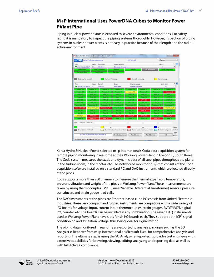
97Application Briefs M+P International Uses PowerDNA Cubes
® United Electronics IndustriesApplications Handbook
Version: 1.0 — December 2013© 2013 United Electronic Industries, Inc.
508-921-4600www.ueidaq.com
M+P International Uses PowerDNA Cubes to Monitor Power PVlant PipePiping in nuclear power plants is exposed to severe environmental conditions. For safety rating it is mandatory to inspect the piping systems thoroughly. However, inspection of piping systems in nuclear power plants is not easy in practice because of their length and the radio-active environment.
Korea Hydro & Nuclear Power selected m+p international’s Coda data acquisition system for remote piping monitoring in real-time at their Wolsong Power Plant in Gyeongju, South Korea. The Coda system measures the static and dynamic data of all steel pipes throughout the plant: in the turbine room, in the reactor, etc. The networked monitoring system consists of the Coda acquisition software installed on a standard PC and DAQ instruments which are located directly at the pipes.
Coda supports more than 250 channels to measure the thermal expansion, temperature, pressure, vibration and weight of the pipes at Wolsong Power Plant. These measurements are taken by using thermocouples, LVDT (Linear Variable Differential Transformer) sensors, pressure transducers and strain gauge load cells.
The DAQ instruments at the pipes are Ethernet-based cube I/O chassis from United Electronic Industries. These very compact and rugged instruments are compatible with a wide variety of I/O boards for voltage input, current input, thermocouples, strain gauges, RVDT/LVDT, digital I/O, counter, etc. The boards can be installed in any combination. The seven DAQ instruments used at Wolsong Power Plant have slots for six I/O boards each. They support both ICP® signal conditioning and excitation voltage, thus being ideal for signal mixing.
The piping data monitored in real-time are exported to analysis packages such as the SO Analyzer e-Reporter from m+p international or Microsoft Excel for comprehensive analysis and reporting. The ultimate step is using the SO Analyzer e-Reporter. It provides test engineers with extensive capabilities for browsing, viewing, editing, analyzing and reporting data as well as with full ActiveX compliance.

98Application Briefs M+P International Uses PowerDNA Cubes
® United Electronics IndustriesApplications Handbook
Version: 1.0 — December 2013© 2013 United Electronic Industries, Inc.
508-921-4600www.ueidaq.com
Coda supports compact I/O chassis
Coda is a full-featured turnkey software platform for data acquisition, signal analysis and pro-cess monitoring from tens to thousands of input channels. The intuitive graphical user interface facilitates set-up, operation and analysis, thus leading to precise, repeatable results quickly. The interface queries the DAQ instruments and preloads information regarding specific parameters such as channel count, gain ranges, filter selections and sample rates.
Sophisticated analysis and reporting using m+p’s SO Analyzer e-Reporter software
The extensive built-in features and tools offer a functionality that was previously available only in custom packages. These features include intuitive configuration tools, user-definable chan-nel groups, automatic instrument identification, real-time alarm monitoring and limit checking, sophisticated data interpretation and display, online graphical data analysis and comprehen-sive visualization.
The client/server architecture allows shared use of the acquired data, enabling several test engineers to have concurrent online access for data display and analysis operations.

99Application Briefs FlightSafety International’s RACKtangle-Based Sim I/O
® United Electronics IndustriesApplications Handbook
Version: 1.0 — December 2013© 2013 United Electronic Industries, Inc.
508-921-4600www.ueidaq.com
FlightSafety International’s RACKtangle-Based Sim I/OAbstract:There are a variety of factors that determine the viability of a new flight simulator. Chief among these are performance, uptime/availability, maintainability and ease of use. This paper will dis-cuss how FlightSafety engineers, working in close conjunction with the UEI engineering team, have deployed UEI’s “RACKtangle™” I/O series and made across the board improvements in the new SimI/O equipped simulators
Introduction: Piloting an aircraft without training is an inherently dangerous endeavor. Though early aviation pioneers were forced to take this risk or stay on the ground, this is no longer the case. Almost all pilots start their training in single engine, piston powered aircraft accompanied by a flight instructor. Most advanced training, and in particular, training of professional pilots in turbine powered aircraft, is now performed in a simulator.
Flight simulators offer a number of key advantages over training in actual aircraft. First and foremost is safety. It’s possible to simulate almost any emergency or system failure in a simulator without risking life or limb. The same is certainly not true in an actual aircraft. It’s perfectly safe for a student pilot to experience an engine failure on takeoff in a simulator. If the student is slow to abort the takeoff and the simulator runs off the runway, no damage is done (except to egos).
Another key advanttage of flight simulator training is the cost savings of simulated flight versus actual. Though simulators are not inexpensive, it’s still much less expensive for a pilot to take his/her “check ride” in a simulator than actually firing up and flying a Boeing, Airbus or other aircraft.
Though there were earlier attempts to build a ground based flight simulator, most consider the Link trainer developed by Edwin Link in 1929 to be the first “real” simulator. Following a number of US Army Air Corps accidents in the early 1930s, the army purchased four of Link’s simulators and the flight simulator industry was born.
FlightSafety International was founded in 1951, dedicated to the principle that aviation safety is best achieved through training. With a fleet of nearly 400 simulators, FlightSafety is the world’s leading supplier of flight simulators. Since the beginning, FlightSafety has been a leader in the developing simulator technology. For simulator training to be economically viable, simulators must:
1. Accurately replicate the “look and feel” of the actual aircraft
2. Provide an extraordinary level of reliability as most simulators are “flown” around the clock and are scheduled out weeks, if not months, in advance.
3. Allow quick repair. Simulators are complex devices and all devices can fail. It is critical to be able to diagnose and repair any failures quickly.
4. Be maintainable. A simulator is an expensive piece of capital equipment. To justify the investment, the simulator must have a long life, and so, must be assembled from components that will be available for many years.
5. Use standardized, well established components so new simulators, and in particular, simulators of new aircraft are developed in a timely manner with a minimum of new “learning curves” to be climbed.
6. Offer attractive pricing. Simulation is a competitive market. In order to prosper, a simulator must be able to offer competitive prices.
FlightSafety’s new SimI/O series simulators have been developed to meet all of the above requirements and more. Though FlightSafety’s current simulators are the highest performance,
100Application Briefs FlightSafety International’s RACKtangle-Based Sim I/O
® United Electronics IndustriesApplications Handbook
Version: 1.0 — December 2013© 2013 United Electronic Industries, Inc.
508-921-4600www.ueidaq.com
most technologically advanced simulators available, the SimI/O equipped simulators serve to further distance FlightSafety from the competition.
In their development of the new series, FlightSafety investigated a host of different I/O vendors and systems. In the end, the company has standardized all computer based I/O on the United Electronic Industries (UEI) RACKtangle I/O chassis and its associated I/O boards.
The remainder of this paper will detail how UEI’s RACKtangle chassis is leveraged to achieve these goals in the new SimI/O series simulators. We will break the discussion down into distinct advantages though you will notice there is frequently an overlap where a particular RACKtan-gle I/O chassis feature has a positive influence on more than one system issue.
High performance: Performance is always an issue on a simulator. Obviously the goal is to make the simulator per-form EXACTLY like the real aircraft. The new RACKtangle I/O equipped simulators have helped FlightSafety enhance the performance of the SimI/O series in a number of ways.
1. The RACKTangle to computer interface is implemented via 1000base-T, Gigabit Ethernet. The Gigabit implementation ensures communications between inputs, the controlling computer and control/display output is fast and does not become a gating issue. Also, the ability to address 12 I/O boards in a single rack, with a single IP address reduces the overhead required to “talk” to the I/O system. The 12-slot rack provides up to 300 analog input, 384 analog output, 696 digital I/O or 144 ARINC-429 channels. The high Gigabit data transfer rate, combined with the low overhead enables system scan/update rates of 2000 Hz. This enhances overall system “smoothness” and allows control algorithms to make smaller, more accurate changes and adjustments.
2. Ensuring there are no “hiccups” or uncommanded “bumps” in the simulator requires the use of a computer with an operating system offering deterministic timing. There is no time to stop the control system algorithms while a disk drive is written or a monitor updated. The SimI/O series utilizes the Ardence RTX® – Real-time Extension for Control of Windows operating system. UEI’s RACKtangle chassis includes complete support for the RTX real time operating system (RTOS) as well as most other popular RTOS including QNX, RT Linux, and RTAI Linux. Though many I/O manufacturers have ignored the Linux/RTOS market or relegated the support to unofficial user forums, UEI drivers are factory written and fully supported.
3. On SimI/O equipped simulators, the I/O chassis are mounted directly on the simulator itself as opposed to previous designs where the actual I/O interfaces were mounted in racks external to the simulator. The on-board location of the SimI/O allows shorter wiring lengths, which decreases noise pickup and increases the system’s overall signal to noise ratio.
High reliability:Whether the simulator is operated by an airline, a government agency, or a training division of FlightSafety, unscheduled simulator down time is a disaster. Not only does it reduce billable/usable hours, it creates schedule chaos. Most simulators are operated “round the clock” and it is extremely difficult, if not impossible, to “make up” time lost by a down Simulator. In particular, pilots of part 121 airlines have extremely tight schedules, and their training schedules are not flexible. A pilot who misses a check ride because the Sim is down is effectively grounded. This not only causes hardship for the pilot, but also the airline, which is then forced to allocate a reserve pilot as a replacement. FlightSafety’s simulators offer a remarkable 99.6% availability. Assuming the simulator is scheduled out 24/7, this represents less than three hours of down time per month. Two key factors determine simulator availability. These are reliability (typically expressed as mean time between failures or MTBF) and repairability (often referred to as mean

101Application Briefs FlightSafety International’s RACKtangle-Based Sim I/O
® United Electronics IndustriesApplications Handbook
Version: 1.0 — December 2013© 2013 United Electronic Industries, Inc.
508-921-4600www.ueidaq.com
time to repair or MTTR). The new RACKtangle I/O solution enhances both MTBF and MTTR. We will discuss the reliability advancements here while repairability topics will be covered in the next section.
The new UEI based SimI/O equipped simulators are designed to improve on FlightSafety’s already extraordinary reliability. Here’s how:
1. Historically, simulators have been installed in two “parts”; the actual simulator and the external control station. All I/O connections had to be wired directly from the sim to the control panel. In complex aircraft, this requires a wiring harness containing over one thousand wires. The fact that the simulators move in 6 degrees of motion greatly complicates this connection and requires the use of a “waterfall” wiring scheme. The high I/O density of the UEI RACKtangle I/O chassis has allowed FlightSafety to build the entire control station into the simulator itself. The waterfall wiring harness on a SimI/O equipped simulator now contains little more than power and Ethernet con-nections. All I/O wiring is fixed in place. The elimination of thousands of moving wires greatly reduces the probability of a broken wire or connector causing a system failure.
2. Today’s aircraft cockpits are filled with annunciator lights and indicators. Turn them on at the same time and the cockpit takes on the look of a Christmas tree. Though there is a movement toward the use of high reliability LED indicators, the bulk of the indica-tors in most aircraft remain incandescent bulbs. Incandescent bulbs left on (or off) are extremely reliable and will last for years. There are reports of a bulb installed at a Texas opera house that has been burning constantly since September or 1908! However, the thermal shock, and corresponding rapid expansion/contraction of bulb filaments as they are turned on/off dramatically reduces bulb life. The Guardian series digital out-put modules installed in the UEI RACKtangle provide a pulse width modulated (PWM) “soft-start” capability. The soft-start allows the bulb filament to be brought up to temperature (and brightness) gradually enough that thermal shock is greatly reduced, yet quickly enough that there is no noticeable impact on the display. This feature dramatically improves bulb life and reduces down time. (Note the PWM feature can be set to run at steady state duty cycles. This allows the digital outputs to also serve as a “virtual rheostat” and allows the outputs to offer a “dimmer” capability in addition to simply turning bulbs on or off.)
Rapid diagnosis and repairs: FlightSafety simulators are remarkably reliable. However, failures in a device as complex as a simulator are inevitable. A critical design goal of the SimI/O equipped simulators is to reduce the mean time to repair once a system or component has failed. UEI’s RACKtangle I/O chassis has enabled FlightSafety to reduce the amount of time required for the repair technician to di-agnose problems. It has also enabled the technicians to make many repairs more quickly. Many failures are now diagnosed and repaired in the amount of time it takes the crew to grab a cup of coffee. In fact, many failures can be fully diagnosed while the sim is still running! Also, the simpler and faster repairs made possible by the new SimI/O diagnostics allow the simulation operator to maintain a smaller, less technically advanced repair and maintenance staff. Here’s how the RACKtangle I/O chassis helps accomplish these goals.
1. Each RACKtangle I/O chassis provides two Ethernet connections, at independent IP addresses. One of the IP addresses is used by the simulator host computers to read and write the I/O. The second is available as a diagnostics “snoop in” port and diag-nostics software may be run while the simulator is actually operational. Many, if not most, simulator failures do not bring the simulator “down”, but merely make certain procedures or functions unavailable. It is often possible for the instructor to move on to a different part of the training syllabus with a “failed” system on board. The ability

102Application Briefs FlightSafety International’s RACKtangle-Based Sim I/O
® United Electronics IndustriesApplications Handbook
Version: 1.0 — December 2013© 2013 United Electronic Industries, Inc.
508-921-4600www.ueidaq.com
to run diagnostics concurrently with actual training will make it possible for the repair technician to identify the cause of a failure, determine which component(s) need replacement, acquire the components from stock, and prepare to perform the repair without stopping the training. Of course it’s unlikely the repair can be made while the Sim is operating. However, since the technician knows exactly what to replace, how to replace it, and has the items in hand before bringing the sim down, the repairs are often made in minutes, not hours.
2. All SimI/O inputs are connected to an internal switch that allows the input to be dis-connected from the live SimI/O and connected to a predefined test signal. Similarly, all SimI/O outputs can be independently monitored. The ability to fully test all I/O automatically dramatically simplifies and speeds up diagnosing any problems identi-fied in the cockpit or via system generated error alarms. This capability also allows complete self-tests and identifies wiring and installation problems without requiring manual wiring and continuity testing. A key aspect of the self diagnostics is the ability for the RACKtangle’s digital outputs to monitor their actual output voltage and cur-rent, while the digital inputs are able to monitor hi and low, but are able to actually measure the input voltage with 25 mV accuracy. This measurement capability makes it possible not only to detect failures, but also to note changes in system behavior that might be predictive of pending failures.
3. The new Ethernet based “diagnostic IP” system enables a standard wireless interface to the technician’s remote, hand-held diagnostic unit. In addition to identifying the problem, the system also provides instant access to any required schematics, user manuals, and/or wiring diagrams.
4. The second diagnostic IP address also supports a Web browser interface allowing a senior technician or engineer to access the system remotely. They can then diagnose and correct any issues beyond the local technician’s capability without requiring any travel or travel related down-time.
5. The modular nature of the RACKtangle, combined with the ability to replace any I/O module in a matter of seconds, greatly reduces repair time. The RACKtangle chassis contains no active components. All I/O modules, the CPU/NIC module and power supply modules are all easily replaced. The new SimI/O system is based upon a small number of standard COTS components, reducing the on-site requirement for spares as well as ensuring fast access to replacement components when necessary.
6. Not all Simulator features and functions are used in every training session. SimI/O’s self test and diagnostic capabilities allow the system to self test between sessions. The engine fire, cabin depressurization, or alternator failure warning annunciators might be used infrequently, but must work when commanded. The self-test features allow these components to be automatically checked. Should a failure be noted, it is pos-sible for the technician to correct the situation between sessions, during scheduled maintenance, or while another repair is made without causing any down-time and without impacting training efficacy.
Extended simulator life:Though efficient and cost effective, there is no debate that a flight simulator is an expensive piece of capital equipment. As such, a purchaser/operator of a flight simulator needs to know the device will be viable far into the future. UEI’s RACKtangle I/O series was the perfect choice as the basis for the I/O requirements in the new SimI/O series. Here’s why.
1. Previous versions of FlightSafety’s flight simulators have been based upon VME technology. Though many vendors remain committed to supporting the VME bus, many others, and in particular those focusing on I/O products are moving on to other

103Application Briefs FlightSafety International’s RACKtangle-Based Sim I/O
® United Electronics IndustriesApplications Handbook
Version: 1.0 — December 2013© 2013 United Electronic Industries, Inc.
508-921-4600www.ueidaq.com
platforms (e.g. Ethernet, LXI, etc.). To ensure long term availability of the hardware required to build new simulators as well as to support those already in the field, it was necessary to switch to a more stable architecture. (Note: FlightSafety has taken the necessary steps to ensure there will not be any disruption in support for exist-ing simulators. Also, if required, it will be possible to retrofit existing simulators with SimI/O hardware.)
2. The Ethernet in its various formats is ubiquitous and has been supported in one form or another since 1980. The Gigabit Ethernet interface currently used in UEI’s RACKtan-gle I/O system is becoming well established in the I/O control environment and will provide a stable communications protocol for many years to come.
3. UEI and FlightSafety are partners in the SimI/O endeavor. Previous simulators have been based upon I/O systems provided by a large number of different vendors. Though FlightSafety’s I/O purchases were significant, they have not always been large enough to justify a particular vendor’s continued production of a given component. This is particularly the case as more and more of the VME based components have been “EOL-end of lifed”. The UEI/FlightSafety partnership ensures a continued supply of product, now and in the future.
4. UEI serves a large number of OEM customers who depend on the company to provide a long-tem, uninterrupted supply of measurement and control products. UEI’s com-mitment is demonstrated daily by the company’s willingness to continue supplying its OEM customers ISA bus boards developed almost 20 years ago. UEI product support has even gone so far as to clone and provide a stable source of I/O boards that have been discontinued by other vendors. UEI is a vendor committed to long term support of its products and its OEM customers.
Timely development of new simulators: Previous simulators have been based on I/O supplied by a variety of vendors. Though this situ-ation was workable, it was not optimal. It mandated developers to use multiple, often dramati-cally different, software and hardware form factors. In the new SimI/O equipped simulators, all I/O hardware and software, including avionics instrument control (AIC), control loading and motion (CLM) and flight deck I/O (FDK) is based upon the UEI RACKtangle I/O series. Here’s how the UEI RACKtangle helps FlightSafety get their new simulators up and running quickly.
1. In the new SimI/O architecture, all I/O is based on the UEI RACKtangle I/O chassis. This chassis allows great flexibility as any of the 25+ available I/O modules may be installed in any of the rack’s 12 I/O slots. The standard form factor and footprint allow FlightSafety to standardize on the I/O and control bay on each simulator and yet have an almost limitless ability to configure the I/O to match the particular aircraft. The RACKtangle provides unprecedented I/O density, including up to 300 analog input, 384 analog output, 144 ARINC-429 channels per rack.
2. The software interface to all of the I/O capability is provided in a single, straightforward API. This dramatically reduces the time required by the software developers to actu-ally write the application programs. It provides portability so application code may be shared among different development groups. It dramatically simplifies software docu-mentation and maintenance as all the I/O is based upon a single driver. Finally, when a driver software update is required, it is achieved by updating a single driver.

104Application Briefs FlightSafety International’s RACKtangle-Based Sim I/O
® United Electronics IndustriesApplications Handbook
Version: 1.0 — December 2013© 2013 United Electronic Industries, Inc.
508-921-4600www.ueidaq.com
Lower cost: Though performance, availability, and supportability are the key issues that drove FlightSafety to standardize on the UEI RACKtangle series, the UEI system also provides all of its advantages and reduces the cost of SimI/O equipped systems relative to previous configurations. The UEI based system reduces overall cost in a number of ways.
1. The UEI RACKtangle I/O costs less than the previous VME based systems.
2. The advanced diagnostics provided in SimI/O equipped simulators dramatically reduce debugging of a newly built simulator. This reduces the time and labor costs required to get a new simulator up and running.
3. Reduced cost of construction due to the reduction in waterfall wiring required. This offers dramatic cost savings both in “parts” cost and in assembly labor. This is of particular note as almost all simulators are built twice. Once at the factory to prove proper operation, and then again at the simulator’s final location in an FlightSafety or customer training facility.
4. The actual size of “on-simulator” equipment cabinet is reduced by over 50%. This re duces the cost of the structure required to support the I/O system.
5. Common I/O and chassis components reduce the requirement for on-site spare prod-ucts. The spares requirement is also reduced as all of the RACKtangle components used in SimI/O equipped simulators are standard COTS products at UEI and there are no long delivery schedules that need to be considered when it comes to planning the stock of spare components.
105Application Briefs Rocket Test Stand with PowerDNA Cube and AI-225
® United Electronics IndustriesApplications Handbook
Version: 1.0 — December 2013© 2013 United Electronic Industries, Inc.
508-921-4600www.ueidaq.com
Rocket Test Stand with PowerDNA Cube and AI-225A large military research facility needed to acquire high speed dynamic data from a rocket test stand. The types of measurements were pressures, pressure differentials, temperature, strain, fluid flow, force, and mechanical strain. The application presented several significant design challenges, starting with a very tight budget, plus stringent requirements for simultaneous sampling of all measurement sensors.
Wide physical separation of sensors and long cable runs to the host computer system also made the use of multiple PowerDNA cubes mounted directly on the test stand — and intercon-nected via Ethernet — a very attractive option.
The need for simultaneous sampling and for running at different scan rates for two classes of sensors were met by using the standard UEI DNA-AI-225 Analog Input Layer. The requirement for per-channel signal conditioning hardware was met by the use of standard UEI accessory panels with individual bridge completion resistors (for strain gauge sensors) and with automatic CJC/Open TC detection for thermocouple inputs. The specification for automatic thermocouple linearization was easily met by the standard UEI Framework software supplied with each Cube.
System DescriptionThe system was designed as an Ethernet distributed network with three multi-layer PowerDNA Cubes, each with up to 6 25-channel Analog Input boards. Each I/O board accepts voltage or millivolt signals from up to 25 strain gauge type sensors and/or thermocouples mounted at various locations throughout the test stand — a total capability of up to 375 inputs. Mounting the Cubes directly on the test stand and using Ethernet for Cube-host communication reduced the need for expensive front-end wiring by almost 80%.
The half-bridge strain gauge sensors are used for measuring pressures, pressure differentials, fluid flow, and mechanical strain. Excitation voltage is provided by a user-supplied power source, the output of which is continuously monitored as a separate analog input.
Product Description / Usage
DNA-PPC8 Ethernet PowerDNA Cubes, each with up to 6 I/O slots. In-cludes UEIDAQ Framework Software Suite.
DNA-AI-225 25-channel, 24-bit simultaneous sampling A/D I/O boards monitor strain gauge sensors and thermocouples.
DNA-STP-AI-U Universal Screw Terminal Panels provide cold junction com-pensation/open TC detection for thermocouple inputs and bridge completion resistors/excitation voltage connections for strain gauge sensors.
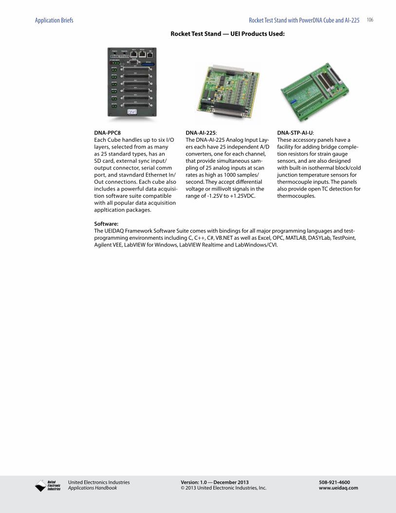
106Application Briefs Rocket Test Stand with PowerDNA Cube and AI-225
® United Electronics IndustriesApplications Handbook
Version: 1.0 — December 2013© 2013 United Electronic Industries, Inc.
508-921-4600www.ueidaq.com
Rocket Test Stand — UEI Products Used:
DNA-PPC8Each Cube handles up to six I/O layers, selected from as many as 25 standard types, has an SD card, external sync input/output connector, serial comm port, and stavndard Ethernet In/Out connections. Each cube also includes a powerful data acquisi-tion software suite compatible with all popular data acquisition appltication packages.
DNA-AI-225:The DNA-AI-225 Analog Input Lay-ers each have 25 independent A/D converters, one for each channel, that provide simultaneous sam-pling of 25 analog inputs at scan rates as high as 1000 samples/second. They accept differential voltage or millivolt signals in the range of -1.25V to +1.25VDC.
DNA-STP-AI-U: These accessory panels have a facility for adding bridge comple-tion resistors for strain gauge sensors, and are also designed with built-in isothermal block/cold junction temperature sensors for thermocouple inputs. The panels also provide open TC detection for thermocouples.
Software: The UEIDAQ Framework Software Suite comes with bindings for all major programming languages and test-programming environments including C, C++, C#, VB.NET as well as Excel, OPC, MATLAB, DASYLab, TestPoint, Agilent VEE, LabVIEW for Windows, LabVIEW Realtime and LabWindows/CVI.
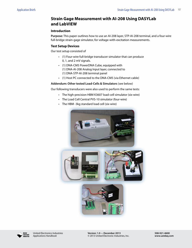
107Application Briefs Strain Gage Measurement with AI-208 Using DASYLab
® United Electronics IndustriesApplications Handbook
Version: 1.0 — December 2013© 2013 United Electronic Industries, Inc.
508-921-4600www.ueidaq.com
Strain Gage Measurement with AI-208 Using DASYLab and LabVIEWIntroductionPurpose: This paper outlines how to use an AI-208 layer, STP-AI-208 terminal, and a four-wire full-bridge strain-gage simulator, for voltage-with-excitation measurements.
Test Setup DevicesOur test setup consisted of
• (1)Four-wirefull-bridgetransducersimulatorthatcanproduce 0, 1, and 2 mV signals.
• (1)DNA-CM5PowerDNACube,equippedwith (1) DNA-AI-208 Analog Input layer, connected to (1) DNA-STP-AI-208 terminal panel
• (1)HostPCconnectedtotheDNA-CM5(viaEthernetcable)
Addendum: Other tested Load-Cells & Simulators (see below)
Our following transducers were also used to perform the same tests:
• Thehigh-precisionHBMK3607load-cellsimulator(six-wire)• TheLoadCellCentralPVS-10simulator(four-wire)• TheHBM-3kgstandardloadcell(six-wire)
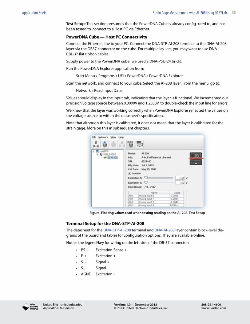
108Application Briefs Strain Gage Measurement with AI-208 Using DASYLab
® United Electronics IndustriesApplications Handbook
Version: 1.0 — December 2013© 2013 United Electronic Industries, Inc.
508-921-4600www.ueidaq.com
Test Setup: This section presumes that the PowerDNA Cube is already config- ured to, and has been tested to, connect to a Host PC via Ethernet.
PowerDNA Cube — Host PC ConnectivityConnect the Ethernet line to your PC. Connect the DNA-STP-AI-208 terminal to the DNA-AI-208 layer via the DB37 connector on the cube. For multiple lay- ers, you may want to use DNA-CBL-37 flat ribbon cables.
Supply power to the PowerDNA cube (we used a DNA-PSU-24 brick).
Run the PowerDNA Explorer application from:
Start Menu » Programs » UEI » PowerDNA » PowerDNA Explorer
Scan the network, and connect to your cube. Select the AI-208 layer. From the menu, go to:
Network » Read Input Data:
Values should display in the Input tab, indicating that the layer is functional. We incremented our precision voltage source between 0.0000V and 1.2500V, to double-check the input line for errors.
We knew that the layer was working correctly when PowerDNA Explorer reflected the values on the voltage source to within the datasheet’s specification.
Note that although this layer is calibrated, it does not mean that the layer is calibrated for the strain gage. More on this in subsequent chapters.
Figure: Floating values read when testing reading on the AI-208. Test Setup
Terminal Setup for the DNA-STP-AI-208The datasheet for the DNA-STP-AI-208 terminal and DNA-AI-208 layer contain block-level dia-grams of the board and tables for configuration options. They are available online.
Notice the legend/key for wiring on the left side of the DB-37 connector:
• PS..+ ExcitationSense+• P..+ Excitation+• S..+ Signal+• S..- Signal-• AGND Excitation-

109Application Briefs Strain Gage Measurement with AI-208 Using DASYLab
® United Electronics IndustriesApplications Handbook
Version: 1.0 — December 2013© 2013 United Electronic Industries, Inc.
508-921-4600www.ueidaq.com
Measuring with DASYLabDASYLab Setup: You should have the PowerDNA and Framework drivers (both included in the PowerDNA Software Suite) installed; a menu “UeiDAQ” should be visible in the DASYLab menubar:
Select the “Analog Input” module from UeiDAQ menu:
Click in an open space on the worksheet to drop the AI module. Select PowerDNA > Add De-vice... and add your Cube’s IP.
Browse the Cube devices to select the AI channels you want to use:

110Application Briefs Strain Gage Measurement with AI-208 Using DASYLab
® United Electronics IndustriesApplications Handbook
Version: 1.0 — December 2013© 2013 United Electronic Industries, Inc.
508-921-4600www.ueidaq.com
An Analog Input block is created. Double click on this block to open the property page:
Notice the arrow on the right-hand side with a + sign. This adds more channels; you may do this later—first set up this first channel.
Under Channel Setup, change the Measurement type to Voltage with Excitation.
In the Channel Setup’s measurement configuration:
• SelectbridgetypeasFullBridgefromthedrop-downlist.• SettheInputModetoDifferential• ChecktheScaletomVcheckbox• Setlowandhighmeasurementlimitsforthetransducer.Mytransducerhasa
range of 0 to 2mv, so I will use –1 to 3 mV/V for my example. This automatically sets the gain.
• Settheexcitationvoltageforthebridge;takecare,assettinganevenchannel’sexcitation voltage changes all even channels excitation voltage. The same ap-plies to odd channels.
Your final channel setup should resemble the following:
Note: Changing the excitation voltage for a even layer changes the excitation voltage for all even layers; for odd the change applies to all odd layers.
Click OK to commit the changes to the Channel Setup. Click OK again to accept the Analog Input setup.
Next, adjust the timing type from the menu:
UeiDaq»Hardware Setup

111Application Briefs Strain Gage Measurement with AI-208 Using DASYLab
® United Electronics IndustriesApplications Handbook
Version: 1.0 — December 2013© 2013 United Electronic Industries, Inc.
508-921-4600www.ueidaq.com
A selection page will allow tuning data acquisition settings:
Note: Strain gage measure- ments are a slow process. Select the more flexible Soft- ware Clock, and let DASYLab determine the time base. We can set up a hardware clock later, if necessary.
To adjust the time base (sampling rate), from the menu:
UeiDAQ»Measurement Setup
Select the “DASYLab” tab, and adjust your sample rate. The setting for our measurement is 10 Hz; as there is less hardware noise at lower sampling rates, and thermocouples do not require a high sampling rate.
Choose a digital meter for output – select from the menu:
Module»Display»Digital MeterWhen the Digital Meter block is created, con-nect the output of the Analog Input Block to the input of the Digital Meter with a wire (click on O, drag to I):
In the lower-left corner of the screen, a small child window labeled Dig.Meter00 will be mini-mized. You may select this window and restore it. Creating a Digital Meter will help debug channels when they do not display on the graph. This digital meter may also be set up to display microstrain.
Bring the main DASYLab window into focus.*Alternatively, a Chart Recorder graph works equally well:
Modules » Display » Chart Recorder
Connect the Chart Recorder to the line conn ecting the Digital Meter module to the UeiDaq AI module.
The experiment is now ready to be run!

112Application Briefs Strain Gage Measurement with AI-208 Using DASYLab
® United Electronics IndustriesApplications Handbook
Version: 1.0 — December 2013© 2013 United Electronic Industries, Inc.
508-921-4600www.ueidaq.com
Running the experiment under DASYLabRun the program by pressing the Start Button. This is the very first button in the toolbar. This action begins the experiment.
The digital meter or recorder set up earlier should display the information as soon as the button is pressed, as should the digital meter.
Here are the results for the following setup:
• (1)Four-wirefull-bridgetransducersimulatorthatcanproduce 0, 1, and 2 mV/V signals.
• (1)DNA-CM5PowerDNACube,equippedwith • (1)DNA-AI-208AnalogInputlayer,connectedto • (1)DNA-STP-AI-208terminalpanel
• (1)HostPCconnectedtotheDNA-CM5(viaEthernetcable) running DASYLab with parameters:
More controlled results with DASYLabThe following setup provides accurate, corrected results:
The setup consists of a filter, scaler, display, average, write data module:
• The10thorderButterworthlow-pass(100Hz)Filtersmoothesoutthesignal• TheScalingmoduleusesLinearInterpolationtozero/slopetheline;thefirst
channel corrects both slope and zero, the second only zeroes the line• DigitalDisplaytooutputthetwocorrectedandrawanaloginputvalues• Theaveragemoduleaveragesoneminuteofdata,andsendsittothevwrite mod-
ule, which in turn saves the data to an ASCII file (for excel)

113Application Briefs Strain Gage Measurement with AI-208 Using DASYLab
® United Electronics IndustriesApplications Handbook
Version: 1.0 — December 2013© 2013 United Electronic Industries, Inc.
508-921-4600www.ueidaq.com
1. Adding Filtering:Modules » Signal Analysis » Filter
v
2. Adding ScalingModules » Mathematics » Scaling
3. Adding a Digital DisplayModules » Display » Digital Meter

114Application Briefs Strain Gage Measurement with AI-208 Using DASYLab
® United Electronics IndustriesApplications Handbook
Version: 1.0 — December 2013© 2013 United Electronic Industries, Inc.
508-921-4600www.ueidaq.com
4. Reducing data in a file with a Averaging ModuleModules » Data Reduction » Average
5. Sending the results to a text file (or Excel) Modules » Files » Write Data
File Format: ASCII
Write Protection: Enabled
Multi-File… » Write As Multi File: Enabled » OK
File Name… » Desktop\thermo.txt
(it will be autosplit)

115Application Briefs Strain Gage Measurement with AI-208 Using DASYLab
® United Electronics IndustriesApplications Handbook
Version: 1.0 — December 2013© 2013 United Electronic Industries, Inc.
508-921-4600www.ueidaq.com
Measuring with LabVIEW
LabVIEW SetupThe UeiDaq Framework comes bundled with a variety of examples for test environments. The examples are accessible via the Start Menu:
Start Menu » Programs » UEI » Framework » Examples(From the LabVIEW Examples, select Acquire & Chart PointByPoint Load Cell.VI)
Here is how to set up a strain-gage measurement in LabVIEW:Use PowerDNA Explorer to determine the target cube’s IP and device number,
for example: pdna://192.168.100.2/Dev0/Ai3. This resource string indicates that the IP address of the cube is 192.168.100.2, the AI-208 layer appears as [0] 208 in PowerDNA Explorer, and my strain gage is on Analog Input channel 3.
Next, choose the usable voltage range for the load cell. The gain will be set transparently by the Framework. The max input range is –10 to 10V (gain = 1), up to a gain of 800 (+/-12.5mV) with a resolution of 18 bits (3.81 μV).
Finally, set the refresh rate in milliseconds; strain-gage measurements are usually taken slowly, so a acquisition rate of 10Hz (100ms) is usually adequate.
Modify the other settings in accordance with your sensor type. When the experiment is set up:
Operate > Run
Begins the experiment:

116Application Briefs Thermocouple Measurement with AI-225 Using DASYLab
® United Electronics IndustriesApplications Handbook
Version: 1.0 — December 2013© 2013 United Electronic Industries, Inc.
508-921-4600www.ueidaq.com
Thermocouple Measurement with AI-225 Using DASYLab and .NETIntroductionPurpose: This paper outlines how to use an AI-225 layer, STP-AI-U terminal, and a K-type ther-mocouple, for measuring temperature.
EquipmentOur setup consisted of:
(1) Omega K-type thermocouple wire (yellow with red stripe)
(1) DNA-CM5 PowerDNA Cube, equipped with(1) DNA-AI-225 Analog Input layer, connected to(1) DNA-STP-AI-U terminal panel via(1) Shielded, rounded, DNA-CBL-62 cable
(1) Host PC connected to the DNA-CM5 (via Ethernet cable)
The DNA-AI-225 layer with the DNA-STP-AI-U terminal is ideal for thermocouple measurement. For a good thermocouple, accurate temperature changes can be measured to within 0.1°C!
The DNA-AI-225 layer provides an input range of ±1.25 in 0.059μV increments (24-bit resolu-tion), differential input, sample rates of 5 to 1,000 per second, and a dedicated CJC channel.
CJC, or cold-junction compensation, adjusts the offset caused by connecting different metal types (e.g. the thermocouple wires, and the terminal’s connector block). In detail, a thermocou-ple is essentially two different types of metal wire connected at one end; the two thermocouple wires are screwed into the terminal block (yet another metal), forming another thermocouple at the junction. To remove the offvset of this extra junction, the layer uses the STP-AI-U ter-minal’s on-board IC (wired through the dedicated CJC channel) to determine and remove the extra offset. This method is “built-in” CJC compensation. For non-STP-AI-U connections, “con-stant” CJC compensation is used instead.
Test Setup: This section presumes that the PowerDNA Cube is already configured and tested to connect to a Host PC via Ethernet.
PowerDNA Cube Host PC ConnectivityConnect the Ethernet line to your PC. Connect the DNA-CBL-62 cable to the DNA-STP-AI-U terminal, and to the DNA-AI-225 layer.
Supply power to the PowerDNA cube (we used a DNA-PSU-24 brick).Run the PowerDNA Ex-plorer application from:
Start Menu » Programs » UEI » PowerDNA » PowerDNA Explorer
Scan the network, and connect to your cube. Select the AI-225 layer. From the menu, go to: Network » Read Input Data:
Values should display in the Input tab, indicating that the layer is functional. We incremented our precision voltage source between 0.0000V and 1.2500V, to double-check the input line for errors.
We knew that the layer was working correctly when PowerDNA Explorer reflected the values on the voltage source.
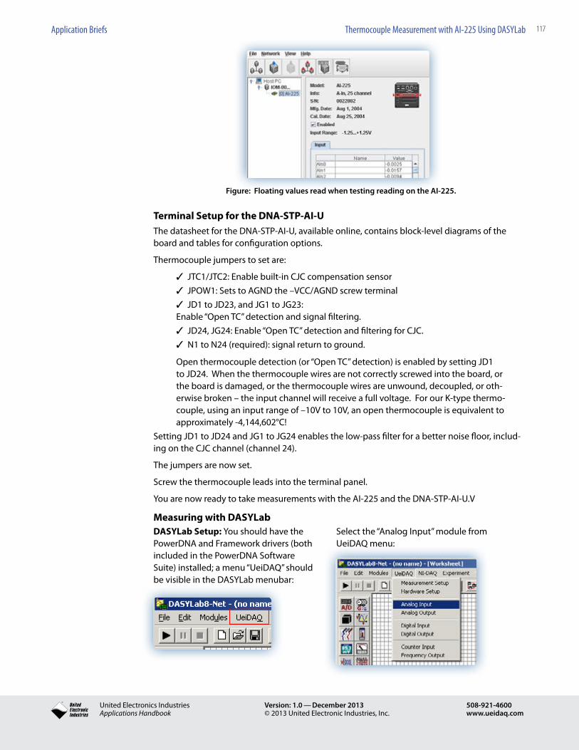
117Application Briefs Thermocouple Measurement with AI-225 Using DASYLab
® United Electronics IndustriesApplications Handbook
Version: 1.0 — December 2013© 2013 United Electronic Industries, Inc.
508-921-4600www.ueidaq.com
Figure: Floating values read when testing reading on the AI-225.
Terminal Setup for the DNA-STP-AI-UThe datasheet for the DNA-STP-AI-U, available online, contains block-level diagrams of the board and tables for configuration options.
Thermocouple jumpers to set are:
3 JTC1/JTC2: Enable built-in CJC compensation sensor3 JPOW1: Sets to AGND the –VCC/AGND screw terminal3 JD1 to JD23, and JG1 to JG23: Enable “Open TC” detection and signal filtering.3 JD24, JG24: Enable “Open TC” detection and filtering for CJC.3 N1 to N24 (required): signal return to ground.
Open thermocouple detection (or “Open TC” detection) is enabled by setting JD1 to JD24. When the thermocouple wires are not correctly screwed into the board, or the board is damaged, or the thermocouple wires are unwound, decoupled, or oth-erwise broken – the input channel will receive a full voltage. For our K-type thermo-couple, using an input range of –10V to 10V, an open thermocouple is equivalent to approximately -4,144,602°C!
Setting JD1 to JD24 and JG1 to JG24 enables the low-pass filter for a better noise floor, includ-ing on the CJC channel (channel 24).
The jumpers are now set.
Screw the thermocouple leads into the terminal panel.
You are now ready to take measurements with the AI-225 and the DNA-STP-AI-U.V
Measuring with DASYLabDASYLab Setup: You should have the PowerDNA and Framework drivers (both included in the PowerDNA Software Suite) installed; a menu “UeiDAQ” should be visible in the DASYLab menubar:
Select the “Analog Input” module from UeiDAQ menu:

118Application Briefs Thermocouple Measurement with AI-225 Using DASYLab
® United Electronics IndustriesApplications Handbook
Version: 1.0 — December 2013© 2013 United Electronic Industries, Inc.
508-921-4600www.ueidaq.com
Click in an open space on the worksheet to drop the AI module. Select PowerDNA > Add Device... and add your Cube’s IP.:
Browse the Cube devices to select the AI chan-nels you want to use:
An Analog Input block is created.
Double click on this block to open the property page:
Press the Channel Setup button to adjust the Analog Input parameters (changes are applied to the currently selected channel!)Under Channel Setup, change the Measurement type to Thermocouple.
Set up the measurement configuration:
- Select your Thermocouple type from the drop-down list.- Select the Temperature scale for output- For the AI-225 with STP-AI-U, select CJC type: Built-in
otherwise, select the Constant and fill in the CJC constant- Set the Input Mode to Differential
Note: Changing the “low limit” and “High limit” parameters will adjust the gain of the analog input amplifier
Click OK to commit the changes to the Channel Setup. Click OK again to accept the Analog Input setup.
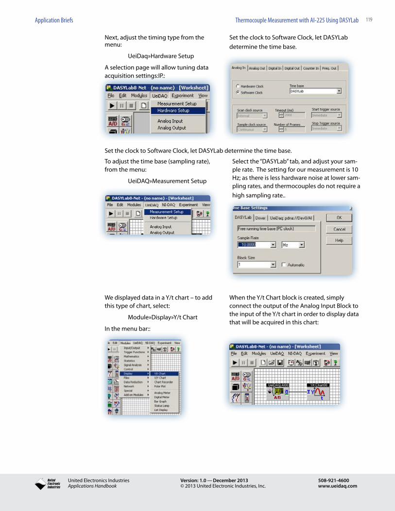
119Application Briefs Thermocouple Measurement with AI-225 Using DASYLab
® United Electronics IndustriesApplications Handbook
Version: 1.0 — December 2013© 2013 United Electronic Industries, Inc.
508-921-4600www.ueidaq.com
Next, adjust the timing type from the menu:
UeiDaq»Hardware Setup
A selection page will allow tuning data acquisition settings:IP.:
Set the clock to Software Clock, let DASYLab determine the time base.
Set the clock to Software Clock, let DASYLab determine the time base.
To adjust the time base (sampling rate), from the menu:
UeiDAQ»Measurement Setup
Select the “DASYLab” tab, and adjust your sam-ple rate. The setting for our measurement is 10 Hz; as there is less hardware noise at lower sam-pling rates, and thermocouples do not require a high sampling rate..
We displayed data in a Y/t chart – to add this type of chart, select:
Module»Display»Y/t Chart
In the menu bar::
When the Y/t Chart block is created, simply connect the output of the Analog Input Block to the input of the Y/t chart in order to display data that will be acquired in this chart:

120Application Briefs Thermocouple Measurement with AI-225 Using DASYLab
® United Electronics IndustriesApplications Handbook
Version: 1.0 — December 2013© 2013 United Electronic Industries, Inc.
508-921-4600www.ueidaq.com
Select the Y/t Chart window and restore it (or maximize it) so that it is visible and usable.
From the Y/t Chart’s menu, select:
Axes » Y Scale...
The default graph will display -5° to 5°. Adjust the axes of the chart to display a range from 0° to 100°. Click OK to commit the changes.
Alternatively, a Chart Recorder graph works equally well:
Modules » Display » Chart Recorder
Bring the main DASYLab window into focus. Creating a Digital Meter will help debug channels when they do not display on the graph.
From the menu:
Modules » Display » Digital Meter.
Connect the Input channel’s output into the Digital Meter’s input.
The experiment is now ready to be run.
Running the experiment under DASYLabRun the program by pressing the Start Button. This is the very first button in the toolbar. This action begins the experiment.
The Y/t chart or recorder set up earlier should display the information as soon as the button is pressed.
Here are the results for the following setup:
(1) Omega K-type thermocouple wire (yellow with red stripe)(1) DNA-CM5 PowerDNA Cube, equipped with (1) DNA-AI-225 Analog Input layer, connected to a DNA-STP-AI-U terminal panel via a shielded, rounded, DNA-CBL-62 cable(1) Host PC connected to the DNA-CM5 (via Ethernet cable) running DASYLab with parameters: 10 Hz Sample Rate in Software Mode Channel 0 Setup: Differential, K-type TC, °F, Built-in CJC

121Application Briefs Thermocouple Measurement with AI-225 Using DASYLab
® United Electronics IndustriesApplications Handbook
Version: 1.0 — December 2013© 2013 United Electronic Industries, Inc.
508-921-4600www.ueidaq.com
Note the quantity of noise on the output line. Even in differential mode, the noise picked up by a long piece of wire (that behaves like an anten-na) is not easily overcome.
Adding a 1uF to 10uF ceramic capacitor in parallel with the thermocouple reduces the band-width of the noise, in addition to the JDx/JGx jumpers.
Thicker wire (20-22 gauge from 28gauge) helps resist noise.
Running the experiment at lower frequency also helps reject noise at the AI-22.5
Sending the results to a text file (or Excel) Modules » Files » Write Data
File Format: ASCII
Write Protection: Enabled
Multi-File… » Write As Multi File: Enabled » OK File Name… » Desktop\thermo.txt
(it will be autosplit)
This completes the DASYLab how-to.
Measurement and Results with .NETThe PowerDNA and Framework drivers (both included in the PowerDNA Software Suite) must be installed before continuing.
Note that all examples work with MsVS.NET including 2005 Express. For a free copy of VB.NET 2005, visit Microsoft’s MSDN site:
http://msdn.microsoft.com/vstudio/express/vb/download/
Quick results using VB.NETMeasuring thermocouples is a low-speed analog input operation that can be done by modify-ing any analog input example written for MsVS.NET. This section on how to do this for Visual Basic .NET.
Open the Visual Basic.NET examples folder:
Start » Programs » UEI » Framework » Examples » Visual Basic.NET Examples
Thermocouple readings are normally read very slowly, so single point-by-point acquisition suf-fices – use the SingleAI example.

122Application Briefs Thermocouple Measurement with AI-225 Using DASYLab
® United Electronics IndustriesApplications Handbook
Version: 1.0 — December 2013© 2013 United Electronic Industries, Inc.
508-921-4600www.ueidaq.com
OpentheSingleAIexample:double-clickthevb_examples.slnfile.
Right-click the SingleAI project, and select Set as Startup Project; this sets this project as the compile-able project.
You may copy and comment out the lines for Channel configuration before changing it:
// mySs.CreateAIChannel(“pdna://192.168.0.61/Dev2/Ai0:3”, -10.0, 10.0, UeiDaq.AIChannelInputMode.Differential)
Change the Channel configuration line to work with thermocouples:
(where 192.168.100.2 is the cube’s IP address)
mySs.CreateTCChannel(“pdna://192.168.100.2/Dev0/Ai2”, -10.0, 10.0, AIChannelInputMode.Differential, TemperatureScale.Fahrenheit, ColdJunc-tionCompensationType.BuiltIn, 70, “”, AIChannelInputMode.Differential)
That’s it! Now an explanation of why we use this mode, and how it works:
Open the UEIDAQ .NET Documentation from:
Start » Programs » UEI » Framework » Documentation » UeiDaq Framework Documentation
and select help on UeiDaq::CUeiTCChannel from the Class List.
Notice from the documentation that the TC Channel configuration is essentially an enhanced AI Channel configuration that performs linearization and voltage-to-degrees translation for you. The function parameters are:
(“resource string”, min voltage, max voltage, ThermocoupleType, TemperatureScale, ColdJunctionCompensationType, cjcConstant, cjcResource, AIChannelInputMode)
As discussed in the manual, the resource string is, for example:
pdna://192.168.100.2/dev0/Ai2
or, in abstract terms:
<driver>://<IP address>/<layer number>/<analog input, channel 2>
If you are using a non-standard board/setup, bypass channel validation by using a plus in front of the channel, as follows:
pdna://192.168.100.2/dev0/Ai+24
The minimum and maximum voltage automatically sets the gain.
Thermocouple type can be Type B, E, J, K, N, R, S, or T
CJC Compensation Type can be built-in (for the STP-AI-U w/ AI-225) or otherwise constant (in which case, cjcConstant must be defined as the ambient temperature of the room – e.g. 70°F). Otherwise, a cjcResource can be defined.
AIChannelInputMode can be set to differential (AI-225 only works in this mode) or single-ended (for SE-only boards with; connecting one lead to ground – not recommended due to noise).
That’s it! Compile, and run.
123Application Briefs Using Accelerometers in a Data Acquisition System
® United Electronics IndustriesApplications Handbook
Version: 1.0 — December 2013© 2013 United Electronic Industries, Inc.
508-921-4600www.ueidaq.com
Using Accelerometers in a Data Acquisition Systemby Bob Judd Director of Marketing United Electronic Industries, Inc.
Accelerometers are widely used in industry for measuring vibration in rotating machinery, moving vehicles, aircraft, and in structures. Virtually all accelerometer devices use the force generated by moving a seismic mass to measure acceleration of the mass. The displacement of the mass or the force developed by the motion of the mass is detected and measured by a very wide range of sensors, such as electromagnetic, electrostatic, magnetic reluctance, inductive (LVDT), piezoelectric, piezoresistive, potentiometric, capacitance, strain gauge, servo force-balance and motion-balance, and micromachined semiconductors (MEMS).
New types of accelerometers and integrated sensor systems are now replacing more traditional vibration sensors for a number of reasons such as lower cost, better performance, rugged design, and smaller size. The new devices offer increased sensitivity, a wider range of operating frequencies, and much wider range of application in industry.
This paper describes the most popular and widely used types of accelerometers now in com-mon industrial use, compares their typical performance specifications, shows how they are used in typical data acquisition applications, and points the reader to sources of more detailed reference information.
Popular Types of AccelerometersThe most common types of accelerometers or vibration sensors in use today are:
• Piezoelectricaccelerometers(ICPandchargeoutputdevices)• Piezoresistiveaccelerometers(ICPandIEPEoutputdevices)• Straingaugeaccelerometers(bridgeoutputdevices)• MEMSaccelerometers(PWM,highimpedanceanalogvoltage,andbridgeoutput
devices) Piezoelectric Sensors
Piezoelectric sensorsPiezoelectric sensors use Newton’s Second Law (F=ma) and the piezoelectric effect to measure acceleration of a mass. A piezoelectric accelerometer contains a “seismic mass” mounted so that the force applied to the mass by movement of the housing “squeezes” or stresses a natural quartz crystal or man- made piezoelectric ceramic measuring element. The pressure on the measuring element produces an electrical charge within the material that is proportional to the force applied — the piezoelectric effect. This force, in turn, is proportional to acceleration (F=ma). The charge output is a high impedance signal that can be measured directly or ampli-fied and conditioned by other electronic circuits. When supplied without additional signal conditioning circuits, the unit is called a “charge sensor”. It is characterized by a very high inner impedance, low output signal, and no steady-state response. When the device is supplied with built-in preamplifier/impedance converter, it is called an Integrated Electronic Piezo-Electric sensor (IEPE sensor). Integrated vibration sensors supplied by PCB Piezotronics, Inc. use a registered trademark, ICP. The signal conditioning circuits may also be designed to convert the measurement from acceleration to velocity or to displacement.
Because the charge eventually bleeds off through the internal insulation resistance, piezoelec-tric sensors are not suited for true static measurements. They can, however, function accurately at very low frequencies, depending on the characteristics of the piezoelectric material used.

124Application Briefs Using Accelerometers in a Data Acquisition System
® United Electronics IndustriesApplications Handbook
Version: 1.0 — December 2013© 2013 United Electronic Industries, Inc.
508-921-4600www.ueidaq.com
10 100 1000 10000 100000Frequency - Hz
Am
plitu
de
Rat
io o
f O
utpu
t to
Inpu
t
Natural Resonance Frequency
Usable Range
Figure 1. Typical Response Curve of a Piezoelectric Vibration Sensor
The piezoelectric units use natural quartz crystals or man-made ceramic elements to meet vary-ing performance requirements, as shown in the following table, which compares characteristics of quartz and ceramic crystals.
Table 1. Ceramic Crystals vs. Quartz Crystals
Ceramic Crystals Quartz Crystals
Man made crystals Natural Crystals
High Output Sensitivity Low Output Sensitivity
Less Expensive More Expensiv
Higher pyroelectric effect at high temperatures Lower pyroelectric effect at high temperatures
Higher crystal decay rates at high temperatures No crystal decay rate with time or temperature
Lower temperature of operation Higher temperature operation
Mounting Types
Seismic Mass
Strain GaugedElement
IntegralElectronics
Mass
PiezoresistiveSubstrate
IsolatingBase
MassPiezoelectricCrystal
Electronics
PiezoelectricCrystal
Mass
PreloadRing
C. Shear-type Piezoelectric Sensor
A. Single-ended PiezoresistiveCompression Sensor
B. Isolated Piezoelectric Compression Sensor
D. Strain-Gauge Vibration Sensor
Motion
++++++++++ ++++++++++_ _ _ _ _ _ _ _ _ _ _ _ _ _
Figure 2. Typical Constructions of Commonly-Used Accelerometers Piezoresistive Sensors

125Application Briefs Using Accelerometers in a Data Acquisition System
® United Electronics IndustriesApplications Handbook
Version: 1.0 — December 2013© 2013 United Electronic Industries, Inc.
508-921-4600www.ueidaq.com
Piezoresistive SensorsPiezoresistive accelerometers use a piezoresistive substrate instead of a piezoelectric crystal as shown in Figure 2A. The force generated by the seismic mass changes the resistance of strain gauge elements of a Wheatstone bridge that are etched onto the substrate, which outputs a signal proportional to acceleration. A major advantage of a piezoresistive sensor compared to a piezoelectric sensors is that it can be used to measure acceleration accurately at zero frequen-cy, a true static measurement.
Isolated Piezoelectric SensorsCompression accelerometers can sometimes be affected by strain on the housing. To prevent this from happening, the crystal can be mounted on an isolating washer that isolates the crystal from the base, as illustrated in Figure 2B.
Shear-type Piezoelectric SensorsShear-type accelerometers mount the seismic mass so that the direction of motion of the mass produces a shear load on the crystal instead of a compressive load. This type of construction is recommended for applications such as flexible structures or those subject to extreme base distortion or thermal changes.
Strain Gauge SensorsA modern strain gauge accelerometer typically uses a silicon or foil strain gauge deposited on or bonded to an element that flexes or deforms with movement of a seismic mass, as shown in Figure 2D. The strain is detected by a bridge circuit. Like piezoresistive sensors, strain gauge type sensors may also be used for static measurements at zero Hz.
MEMS SensorsThe MEMS sensor (not shown in Figure 2), a relatively new type of sensor developed within the last 15 years for automotive airbag applications, is by far the largest selling and lowest cost type of sensor in use today. Analog Devices, Inc. recently reported selling more than 200-million MEMS sensors for automotive use. Freescale Semiconductor is also a large supplier of MEMS accelerometers for industry.
A MEMS sensor is produced by using micromachining techniques to form minute springs, seismic masses, and motion or force sensing elements from a silicon wafer. When the body of the accelerometer is moved by an externally applied force, the motion of the seismic mass is detected by differential capacitive, piezoresistive, or other types of sensing elements. The signal produced is amplified, conditioned, and filtered by circuit components mounted inside the same IC package. The output signal from a MEMS accelerometer can be any of several signal types, such as an analog voltage, a digital PWM signal, or an SPI serial pulse train. The digital signals eliminate the need for an A/D converter in the data acquisition system.
MEMS sensors, which are available in many different types and ranges, may be used for inertial, vibration, and tilt (DC response) measurement applications. The major advantages of using a MEMS accelerometer are low cost and small size, although some types can be very expensive.
Velocity and Displacement SensorsFor some applications such as monitoring of the health of a rotating machine, velocity or displacement measurement are preferred over acceleration sensing. Since velocity is the first derivative of displacement vs. time, and acceleration is the derivative of velocity, both measure-ments can be calculated from acceleration by integrating the signal once or twice or by using the logarithmic relationships between acceleration, velocity, and displacement as illustrated in Figure 3.

126Application Briefs Using Accelerometers in a Data Acquisition System
® United Electronics IndustriesApplications Handbook
Version: 1.0 — December 2013© 2013 United Electronic Industries, Inc.
508-921-4600www.ueidaq.com
5
10 100 1 k 10 k 100 k1
Acceleration = a
Velocity = aω
aω2Displacement =
Rel
ativ
e Le
vel (
dB)
Frequency - Hz
Figure 3. Logarithmic Relationship Between Acceleration, Velocity, and Displacement
Charge SensorsA piezoelectric sensor supplied without integral signal conditioning circuits is called a charge sensor. It produces a charge output and has a high impedance. A charge sensor is typically re-quired in high temperature or high radiation applications that could damage signal condition-ing components.To overcome this problem, the signal amplifier and associated components are mounted in a safe area at a distance from the charge sensor.
IEPE and ICP AccelerometersIEPE sensors have built-in signal conditioning circuits that have low impedance output elec-tronics compatible with a two-wire constant current supply providing a DC voltage bias. IEPE sensors are very popular in most industrial applications except those with special requirements such as static (zero Hz) sensing, high temperature applications, or process control applications requiring 4-20 mA current outputs.
ICP sensors are “integrated circuit piezoelectric” sensors supplied by PCB Piezotronics, Inc. un-der the trademark, ICP, and are basically the same as IEPE sensors.
The output of an 2-wire IEPE accelerometer is an AC voltage on a DC voltage bias. The DC bias can be removed by inserting a capacitor in series with the output signal. The IEPE unit also requires a constant current supply. A typical circuit is shown in the figure below.
19 to 30VDC
Voltage Output (AC signal)
0V
Constant Current Power Supply (in DAQ system)
R1.58M
Piezoelectric Sensor
AC signal on DC bias voltage
Blocking cap to remove DC biasForce
Figure 4. IEPE Sensor Output Circuit and Constant Current Source
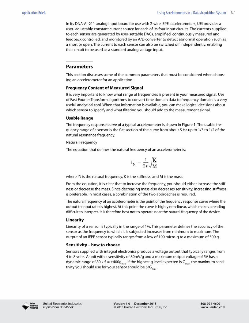
127Application Briefs Using Accelerometers in a Data Acquisition System
® United Electronics IndustriesApplications Handbook
Version: 1.0 — December 2013© 2013 United Electronic Industries, Inc.
508-921-4600www.ueidaq.com
In its DNA-AI-211 analog input board for use with 2-wire IEPE accelerometers, UEI provides a user- adjustable constant current source for each of its four input circuits. The currents supplied to each sensor are generated by user-settable DACs, amplified, continuously measured and feedback controlled, and monitored by an A/D converter to detect abnormal operation such as a short or open. The current to each sensor can also be switched off independently, enabling that circuit to be used as a standard analog voltage input.
ParametersThis section discusses some of the common parameters that must be considered when choos-ing an accelerometer for an application.
Frequency Content of Measured SignalIt is very important to know what range of frequencies is present in your measured signal. Use of Fast Fourier Transform algorithms to convert time domain data to frequency domain is a very useful analytical tool. When that information is available, you can make logical decisions about which sensor to specify and what filtering you should add to the measurement signal.
Usable RangeThe frequency response curve of a typical accelerometer is shown in Figure 1. The usable fre-quency range of a sensor is the flat section of the curve from about 5 Hz up to 1/3 to 1/2 of the natural resonance frequency.
Natural Frequency
The equation that defines the natural frequency of an accelerometer is:
fN1
2π------ K
M-----=
where fN is the natural frequency, K is the stiffness, and M is the mass.
From the equation, it is clear that to increase the frequency, you should either increase the stiff-ness or decrease the mass. Since decreasing mass also decreases sensitivity, increasing stiffness is preferable. In most cases, a combination of the two approaches is required.
The natural frequency of an accelerometer is the point of the frequency response curve where the output to input ratio is highest. At this point the curve is highly non-linear, which makes a reading difficult to interpret. It is therefore best not to operate near the natural frequency of the device.
LinearityLinearity of a sensor is typically in the range of 1%. This parameter defines the accuracy of the sensor as the frequency to which it is subjected increases from minimum to maximum. The output of an IEPE sensor typically ranges from a low of 100 micro-g to a maximum of 500 g.
Sensitivity – how to chooseSensors supplied with integral electronics produce a voltage output that typically ranges from 4 to 8 volts. A unit with a sensitivity of 80mV/g and a maximum output voltage of 5V has a dynamic range of 80 x 5 = ±400gmax. If the highest g level expected is Gmax, the maximum sensi-tivity you should use for your sensor should be 5/Gmax .

128Application Briefs Using Accelerometers in a Data Acquisition System
® United Electronics IndustriesApplications Handbook
Version: 1.0 — December 2013© 2013 United Electronic Industries, Inc.
508-921-4600www.ueidaq.com
The resolution of an accelerometer device in many cases can be improved through the use of digital signal processing techniques, such as oversampling to improve resolution of the sensor, adding digital filters, and automatically calculating/correcting bias offsets and scale errors.
Mounted Natural FrequencyThe natural frequency of an unmounted sensor is different from that of a mounted sensor, be-cause the mounted sensor has a stiffness determined by the stiffness of the structure in which it is mounted. Cementing, bolting, or magnetically attaching the sensor to a structure can lower the natural frequency by a substantial amount.
Sensitivity to Mounting StrainBending, twisting, mechanical or thermal stresses in the base of an accelerometer can cause errors in its measurement output because these stresses can distort a piezoelectric crystal just as an acceleration force does. Single-ended compression sensors are most susceptible to errors caused by strain on the base; shear-type sensors are the least affected. Adding an isolation base to a compression sensor rather than specifying a shear-type sensor is often the best design compromise for most applications.
Triboelectric EffectThe triboelectric effect is the generation of an error signal in a charge output sensor whenever its attached cable is physically moved. The only effective way to eliminate this error signal is to clamp the cable as close to the accelerometer as possible.
Triaxial SensorsTriaxial sensors detect and measure acceleration in all three axes at once. Some units incorpo-rate three separate sensors in a package and others detect 3-axis motion with a single sensor. Separate output signals are provided for each axis of motion.
Tilt SensorsMeasuring tilt is a static sensing task measuring the acceleration of gravity. It requires zero Hz (DC) accuracy and is commonly found in pitch and roll measurements in aircraft or similar applications. To achieve the highest resolution per degree of tilt, the accelerometer should be mounted with its sensitive axis parallel to the plane of movement where the most sensitivity is desired. Such applications usually use 2- (biaxial) or 3-axis (triaxial) accelerometers.
Signal ConditioningThe signal conditioning normally used in an IEPE accelerometer is a low noise regulated con-stant current source to supply a bias voltage to power the sensing device. A blocking capacitor is usually inserted in the output line to remove the DC bias from the sensor signal. The signal fed to the data acquisition system is an AC voltage with amplitude proportional to the ampli-tude of vibration and a frequency the same as the frequency of vibration. Additional signal con-ditioning may be introduced for computing RMS or peak-to-peak measurements, for analyzing the frequency domain spectral content, or for performing snap shot time domain analysis
Low Pass FilterTypically, a low pass filter is used to remove unwanted frequencies present in the sensor signal, such as the natural resonant frequencies of the accelerometer itself.
Ground IsolationCaution must be exercised to prevent ground loops, especially when signal levels are low or where the signal is not amplified. Ground loops may either be eliminated by hard wiring elec-

129Application Briefs Using Accelerometers in a Data Acquisition System
® United Electronics IndustriesApplications Handbook
Version: 1.0 — December 2013© 2013 United Electronic Industries, Inc.
508-921-4600www.ueidaq.com
trical grounds together or prevented by electrically isolating sensors with isolating washers, studs, or bases. Note that use of an isolating mounting may change the natural frequency of the accelerometer.
Choosing a Sensor TypeThe following table lists some factors to consider in choosing an accelerometer:
Type of Accelerometer Advantages Disadvantages
Single-ended Compression RobustHighest natural frequency High shock resistance
Poor base strain performance
Isolated Base Compression RobustHigh natural freqency
Better base strain performance
Shear Best base strain performanceBest temperature transient immunitySmallest size
Less robustLower shock resistance
Charge output High Temperature Operation Suitable for radiation environmentsSmall size
Requires local charge amplifier Sus-ceptible to triboelectric effect
Piezoresistive Measures down to zero Hz. Limited high frequency response
Strain Gauge Measures down to zero Hz. High shock resistance.
Limited high frequency response
Some typical questions to ask in choosing a sensor are listed below:
Will you be measuring an AC variable such as vibration or a DC parameter such as gravity or a constant acceleration?
3 What is the maximum range you expect to measure?3 What is the smallest signal you need to detect?3 What is the maximum frequency you need to measure?3 What level of sensitivity is required for your sensor?3 What power consumption is acceptable?3 What type of mounting will be used?3 What size limitations do you have?
ReferencesThe following is a list of websites that contain information about accelerometers of various types and useful guides to the application of such devices.
www.omega.com
www.coleparmer.com
www.wilcoxon.com
www.endevco.com
www.pcb.com
www.sensormag.com
www.vibrametrics.com
www.sensotec.com
www.analog.com
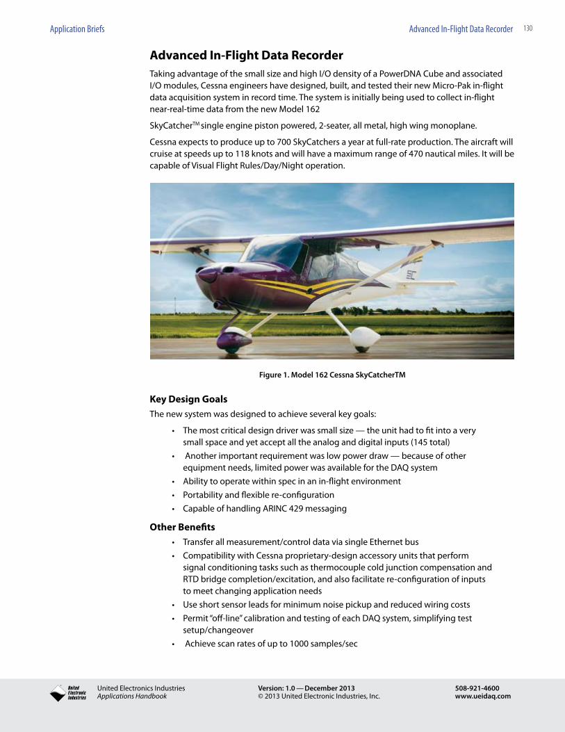
130Application Briefs Advanced In-Flight Data Recorder
® United Electronics IndustriesApplications Handbook
Version: 1.0 — December 2013© 2013 United Electronic Industries, Inc.
508-921-4600www.ueidaq.com
Advanced In-Flight Data RecorderTaking advantage of the small size and high I/O density of a PowerDNA Cube and associated I/O modules, Cessna engineers have designed, built, and tested their new Micro-Pak in-flight data acquisition system in record time. The system is initially being used to collect in-flight near-real-time data from the new Model 162
SkyCatcherTM single engine piston powered, 2-seater, all metal, high wing monoplane.
Cessna expects to produce up to 700 SkyCatchers a year at full-rate production. The aircraft will cruise at speeds up to 118 knots and will have a maximum range of 470 nautical miles. It will be capable of Visual Flight Rules/Day/Night operation.
Figure 1. Model 162 Cessna SkyCatcherTM
Key Design GoalsThe new system was designed to achieve several key goals:
• Themostcriticaldesigndriverwassmallsize—theunithadtofitintoaverysmall space and yet accept all the analog and digital inputs (145 total)
• Anotherimportantrequirementwaslowpowerdraw—becauseofotherequipment needs, limited power was available for the DAQ system
• Abilitytooperatewithinspecinanin-flightenvironment• Portabilityandflexiblere-configuration• CapableofhandlingARINC429messaging
Other Benefits• Transferallmeasurement/controldataviasingleEthernetbus• CompatibilitywithCessnaproprietary-designaccessoryunitsthatperform
signal conditioning tasks such as thermocouple cold junction compensation and RTD bridge completion/excitation, and also facilitate re-configuration of inputs to meet changing application needs
• Useshortsensorleadsforminimumnoisepickupandreducedwiringcosts• Permit“off-line”calibrationandtestingofeachDAQsystem,simplifyingtest
setup/changeover• Achievescanratesofupto1000samples/sec

131Application Briefs Advanced In-Flight Data Recorder
® United Electronics IndustriesApplications Handbook
Version: 1.0 — December 2013© 2013 United Electronic Industries, Inc.
508-921-4600www.ueidaq.com
• UseCOTScomponentstoreduceequipment/installationcostandto increase reliability
• Improvesafety,reliability,maintainability,flexibility,andfacilitateexpandability
The Cessna Micro-Pak system achieves an efficient, high density, and easily configurable system that can meet the data collection requirements for many aircraft types currently being devel-oped at Cessna.
Since the Micro-Pak unit is separable from the aircraft and portable, it can be configured, cali-brated, and tested as an off-line task, independent of the aircraft in which it will be installed. It is then ready for quick setup in a plane whenever the specific type for which it is calibrated is scheduled for a test — without requiring modifications of the aircraft itself.
The requirement for on-board mounting of the data acquisition equipment mandates the use of very compact, rugged, hardware devices with high density input/output capabilities that can operate reliably in the severe environment of in-flight conditions. The on-board mounting design also means very short wire lengths (less than 10 feet) are needed between sensors and DAQ, resulting in much reduced signal noise or loss of signal strength.
In addition, the need for reliable, high speed communication between DAQ and host with mini-mal cabling logically leads to the use of an industry-standard Ethernet network over a single twisted-pair cable — all of which is immediately available with COTS equipment from UEI.
Major DAQ System Equipment ComponentsAs shown in Figure 2, the Miicro-PAK data acquisition system package is an independent module that can be removed from the aircraft as a unit. It can then be configured, calibrated, and tested offline and set aside until needed. It can be quickly installed in and re-configured for any of sev-eral aircraft types and tasks without further modification and can be disconnected from other on-board equipment by simply removing the single Ethernet cable and power connection.
Figure 2 shows a photograph of a Cessna Micro-Pak In-flight DAQ system that shows how com-pact the unit is when assembled and ready for mounting in a 162 SkyCatcher aircraft.
PowerDNA Cube
Host Computer
with 6 Layers
Figure 2. Cessna Micro-Pak In-Flight DAQ System

132Application Briefs Advanced In-Flight Data Recorder
® United Electronics IndustriesApplications Handbook
Version: 1.0 — December 2013© 2013 United Electronic Industries, Inc.
508-921-4600www.ueidaq.com
Front View Rear ViewHost Computer
PowerDNA Cube with 6 Layers
Figure 3. Front and Back Views of Micro-Pak DAQ System
UEI-supplied Data Acquisition System EquipmentFigure 4 illustrates the equipment items used in the Data Acquisition System supplied by UEI. As shown in the diagram, the heart of the DAQ system is a PPC8 PowerDNA Cube. This unit has a PowerPC CPU, SD card slot, DB-9 Serial Port, SD Card slot, several indicating LEDs, and an Eth-ernet interface plus 6 slots for any of over 30 different types of UEI PowerDNA I/O boards that interface with various types of sensors.
The Cube used in the Micro-Pak on-board DAQ system contains the following UEI I/O boards:
• 4 DNA-AI-207 Analog Input BoardsEach unit accepts up to 16 differential input analog voltage inputs. It has an input range of ±10 VDC, programmable gain selection, one 18-bit A/D per board, and a sampling rate of up to 1000 samples/ sec per channel (aggregate maximum of 16 kS/s per board). It also has a dedicated CJC channel for use with thermocouple inputs and automatic offset autozero.In the In-flight Application, the AI-207 boards accept analog inputs from several thermocouples, RTD temperature sensors, pressure, and other analog trans-ducers. These sensors are used to measure various temperatures in the engine, aircraft, and environment, and pressures such as altitude, manifold pressure, engine oil, etc.Cessna also uses two proprietary accessory units that provide special signal conditioning functions for thermocouples and RTDs, and that also enable quick re-configuration of sensors and I/O boards.
•1 - DNA-CT-601 Counter/Timer Input BoardThis unit has 8 independent counter/timer channels that can accept pulse inputs and perform counter tasks such as event counting, width/period measurement, or quadrature encoder measurements.In the In-flight DAQ system application, this board is used to detect pulse rates that indicate current engine RPM and fuel flow.
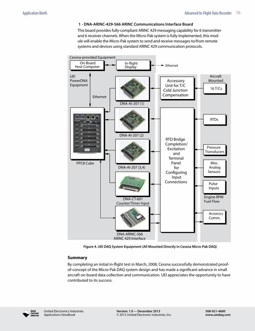
133Application Briefs Advanced In-Flight Data Recorder
® United Electronics IndustriesApplications Handbook
Version: 1.0 — December 2013© 2013 United Electronic Industries, Inc.
508-921-4600www.ueidaq.com
1 - DNA-ARINC-429-566 ARINC Communications Interface BoardThis board provides fully-compliant ARINC 429 messaging capability for 6 transmitter and 6 receiver channels. When the Micro-Pak system is fully implemented, this mod-ule will enable the Micro-Pak system to send and receive messages to/from remote systems and devices using standard ARINC 429 communication protocols.
RTD BridgeCompletion/
Excitationand
TerminalPanel
forCon�guring
InputConnections
Ethernet
Host Computer
PPC8 Cube
DNA-AI-207 (1)
DNA-AI-207 (2)
16 T/Cs
RTDs
PressureTransducers
Accessory
DNA-CT-601Counter/Timer Input
UEI
EthernetOn-Board
PulseInputs
Engine RPMFuel Flow
Misc.Analog
Sensors
Unit for T/C
DNA-AI-207 (3,4)
AircraftMounted
Cold JunctionCompensation
DisplayIn-�ight
PowerDNAEquipment
Cessna-provided Equipment
DNA-ARINC-566ARINC 429 Interface
AvionicsComm.
Figure 4. UEI DAQ System Equipment (All Mounted Directly in Cessna Micro-Pak DAQ)
SummaryBy completing an initial in-flight test in March, 2008, Cessna successfully demonstrated proof-of-concept of the Micro-Pak DAQ system design and has made a significant advance in small aircraft on-board data collection and communication. UEI appreciates the opportunity to have contributed to its success.
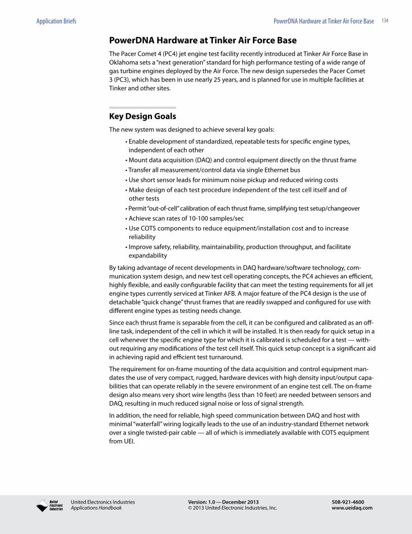
134Application Briefs PowerDNA Hardware at Tinker Air Force Base
® United Electronics IndustriesApplications Handbook
Version: 1.0 — December 2013© 2013 United Electronic Industries, Inc.
508-921-4600www.ueidaq.com
PowerDNA Hardware at Tinker Air Force BaseThe Pacer Comet 4 (PC4) jet engine test facility recently introduced at Tinker Air Force Base in Oklahoma sets a “next generation” standard for high performance testing of a wide range of gas turbine engines deployed by the Air Force. The new design supersedes the Pacer Comet 3 (PC3), which has been in use nearly 25 years, and is planned for use in multiple facilities at Tinker and other sites.
Key Design GoalsThe new system was designed to achieve several key goals:
•Enabledevelopmentofstandardized,repeatabletestsforspecificenginetypes,independent of each other
•Mountdataacquisition(DAQ)andcontrolequipmentdirectlyonthethrustframe•Transferallmeasurement/controldataviasingleEthernetbus•Useshortsensorleadsforminimumnoisepickupandreducedwiringcosts•Makedesignofeachtestprocedureindependentofthetestcellitselfandof
other tests•Permit“out-of-cell”calibrationofeachthrustframe,simplifyingtestsetup/changeover•Achievescanratesof10-100samples/sec•UseCOTScomponentstoreduceequipment/installationcostandtoincrease
reliability•Improvesafety,reliability,maintainability,productionthroughput,andfacilitate
expandability
By taking advantage of recent developments in DAQ hardware/software technology, com-munication system design, and new test cell operating concepts, the PC4 achieves an efficient, highly flexible, and easily configurable facility that can meet the testing requirements for all jet engine types currently serviced at Tinker AFB. A major feature of the PC4 design is the use of detachable “quick change” thrust frames that are readily swapped and configured for use with different engine types as testing needs change.
Since each thrust frame is separable from the cell, it can be configured and calibrated as an off-line task, independent of the cell in which it will be installed. It is then ready for quick setup in a cell whenever the specific engine type for which it is calibrated is scheduled for a test — with-out requiring any modifications of the test cell itself. This quick setup concept is a significant aid in achieving rapid and efficient test turnaround.
The requirement for on-frame mounting of the data acquisition and control equipment man-dates the use of very compact, rugged, hardware devices with high density input/output capa-bilities that can operate reliably in the severe environment of an engine test cell. The on-frame design also means very short wire lengths (less than 10 feet) are needed between sensors and DAQ, resulting in much reduced signal noise or loss of signal strength.
In addition, the need for reliable, high speed communication between DAQ and host with minimal “waterfall” wiring logically leads to the use of an industry-standard Ethernet network over a single twisted-pair cable — all of which is immediately available with COTS equipment from UEI.
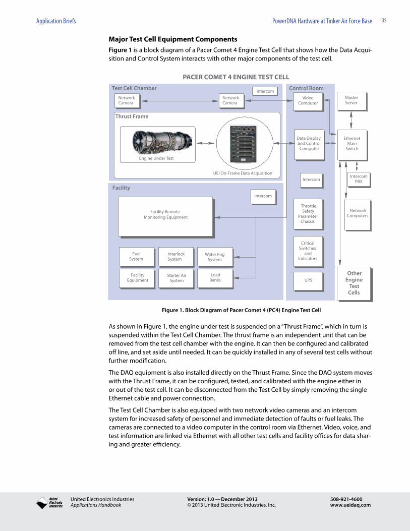
135Application Briefs PowerDNA Hardware at Tinker Air Force Base
® United Electronics IndustriesApplications Handbook
Version: 1.0 — December 2013© 2013 United Electronic Industries, Inc.
508-921-4600www.ueidaq.com
Major Test Cell Equipment ComponentsFigure 1 is a block diagram of a Pacer Comet 4 Engine Test Cell that shows how the Data Acqui-sition and Control System interacts with other major components of the test cell.
OtherEngine
TestCells
VideoComputer
CriticalSwitches
andIndicators
EthernetMain
Switch
ThrottleSafety
ParameterChassis
MasterServer
UPS
Intercom PBX
Intercom PBX
Data Displayand ControlComputer
Facility Remote
FuelSystem
InterlockSystem
Water FogSystem
LoadBanks
Starter AirSystem
FacilityEquipment
WirelessIntercom
Intercom
WirelessIntercom
NetworkCamera
WirelessIntercom
NetworkCamera
Thrust Frame
Test Cell Chamber
UEI On-Frame Data Acquisition
Facility
VideoComputer
Data Displayand ControlComputer
CriticalSwitches
andIndicators
EthernetMain
Switch
NetworkComputers
PACER COMET 4 ENGINE TEST CELL
Control Room
ThrottleSafety
ParameterChassis
MasterServer
UPS
Intercom PBXIntercom
Data Displayand ControlComputer
OtherEngine
TestCells
IntercomIntercom
OtherEngine
TestCells
Engine Under Test
Monitoring Equipment
Figure 1. Block Diagram of Pacer Comet 4 (PC4) Engine Test Cell
As shown in Figure 1, the engine under test is suspended on a “Thrust Frame”, which in turn is suspended within the Test Cell Chamber. The thrust frame is an independent unit that can be removed from the test cell chamber with the engine. It can then be configured and calibrated off line, and set aside until needed. It can be quickly installed in any of several test cells without further modification.
The DAQ equipment is also installed directly on the Thrust Frame. Since the DAQ system moves with the Thrust Frame, it can be configured, tested, and calibrated with the engine either in or out of the test cell. It can be disconnected from the Test Cell by simply removing the single Ethernet cable and power connection.
The Test Cell Chamber is also equipped with two network video cameras and an intercom system for increased safety of personnel and immediate detection of faults or fuel leaks. The cameras are connected to a video computer in the control room via Ethernet. Video, voice, and test information are linked via Ethernet with all other test cells and facility offices for data shar-ing and greater efficiency.

136Application Briefs PowerDNA Hardware at Tinker Air Force Base
® United Electronics IndustriesApplications Handbook
Version: 1.0 — December 2013© 2013 United Electronic Industries, Inc.
508-921-4600www.ueidaq.com
New software developed by the Software Maintenance Group (SMXG) group at Tinker provides fully automatic closed-loop testing for all engine types and versions, plus manual control, utili-ties, and simulation capabilities, all managed through a Graphical User Interface. Test data for all engine types is stored in the Engine Health Management Repository Center data base, which provides baseline performance data for each engine type and also enhances security, safety, and cost effectiveness.
As shown in the block diagram, the control room of the test cell contains the video computer, the data display/control computer, intercom, critical switches/indicators for the engine under test, and an uninterruptible power supply. It also contains the Throttle Safety Parameter Chas-sis, which measures and controls critical parameters required for safe operation (engine core speed, engine fan speed, fuel flow, etc.). If a failure occurs in any subsystem at any time, the throttle safety parameter chassis automatically brings the engine to a safe state.
In addition to the UEI on-frame Data Acquisition/Control System, the Test Facility also contains sensors and related equipment to measure vibration, thrust, load, fuel flow, air flow, rotary and linear position, noise, and other variables. All data collected from remote monitoring equip-ment is transmitted to the Data Display/ Control Computer via Ethernet.
On-Frame Data Acquisition/Control System EquipmentFigure 2 illustrates the equipment items used in the Data Acquisition System supplied by UEI. As shown in the diagram, the engine of the DAQ system is a PPC8 PowerDNA Cube. This unit has a PowerPC CPU, SD card slot, DB-9 Serial Port, SD Card slot, several indicating LEDs, and an Ethernet interface plus 6 slots for any of over 30 different types of UEI PowerDNA I/O boards that interface with various types of sensors.
The Cube used in the on-frame DAQ system contains the following UEI I/O boards:
•1-DNA-AI-225AnalogInputBoard.
This unit accepts up to 25 differential ±1.25 VDC analog inputs. It offers simultaneous sampling of all inputs, one 24-bit A/D for each channel, and a maximum scan rate of 1000 samples/sec per channel. In this specific application, sensor inputs for this board are routed through a uni-versal DNA-STP-AI-U accessory board for signal conditioning and cold junction compensation, as described later in this section.
In the PC4 Test Cell Application, this I/O board acquires data from multiple thermocouples on the engine under test and an RTD that measures engine oil temperature.
• 1DNA-AI-207AnalogInputBoardThis unit accepts up to 16 differential input analog voltage inputs. It has an input range of ±10 VDC, programmable gain selection, one 18-bit A/D per board, and a sampling rate of up to 1000 samples/ sec per channel (aggregate maximum of 16 kS/s per board). It also has a dedicated CJC channel for use with thermocou-ple inputs and automatic offset autozero.In the PC4 Test Cell Application, the AI-207 board accepts voltage inputs from multiple pressure transducers and also from a synchro-to-voltage converter unit measuring engine oil pressure.
•1-DNA-DIO-401DigitalInputBoardThis unit has 24 digital input channels with user programmable hysteresis and an I/O throughput rate of 1000 samples/sec maximum. It has an input FIFO of 1024 samples and requires an external 24 VDC power supply unless a DNA-PC-902 Power Conversion board is supplied with the board.
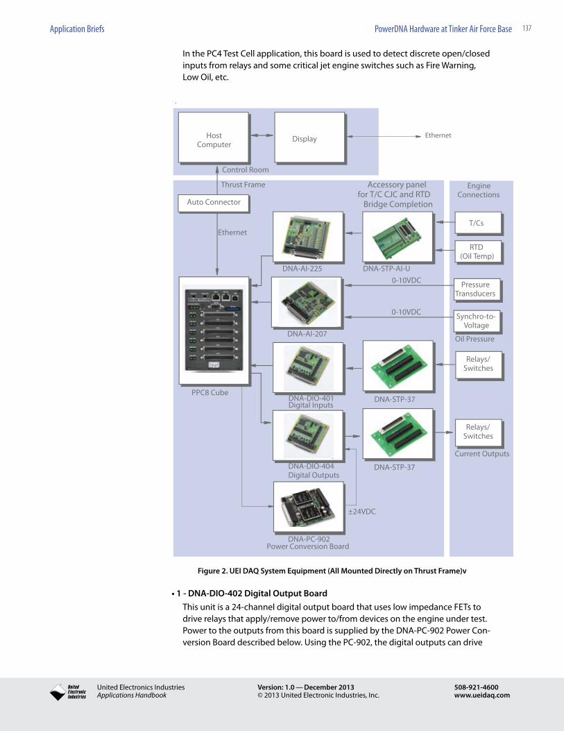
137Application Briefs PowerDNA Hardware at Tinker Air Force Base
® United Electronics IndustriesApplications Handbook
Version: 1.0 — December 2013© 2013 United Electronic Industries, Inc.
508-921-4600www.ueidaq.com
In the PC4 Test Cell application, this board is used to detect discrete open/closed inputs from relays and some critical jet engine switches such as Fire Warning, Low Oil, etc.
.
Ethernet
Host Display
PPC8 Cube
DNA-AI-225 DNA-STP-AI-U
DNA-AI-207
DNA-DIO-401 DNA-STP-37
Relays/Switches
0-10VDC
Computer
T/Cs
RTD(Oil Temp)
PressureTransducers
Accessory panelfor T/C CJC and RTD
Bridge Completion
DNA-DIO-404 DNA-STP-37
Relays/Switches
DNA-PC-902
±24VDC
Auto Connector
Digital Inputs
Digital Outputs
Power Conversion Board
Thrust Frame
Control Room
0-10VDC Synchro-to-Voltage
Oil Pressure
Current Outputs
EngineConnections
Ethernet
Figure 2. UEI DAQ System Equipment (All Mounted Directly on Thrust Frame)v
•1-DNA-DIO-402DigitalOutputBoardThis unit is a 24-channel digital output board that uses low impedance FETs to drive relays that apply/remove power to/from devices on the engine under test. Power to the outputs from this board is supplied by the DNA-PC-902 Power Con-version Board described below. Using the PC-902, the digital outputs can drive

138Application Briefs PowerDNA Hardware at Tinker Air Force Base
® United Electronics IndustriesApplications Handbook
Version: 1.0 — December 2013© 2013 United Electronic Industries, Inc.
508-921-4600www.ueidaq.com
350mA/channel (max peak of 500mA). The board also provides a 512 sample FIFO and offers user-programmable hysteresis on each of the outputs, which significantly improves noise immunity. An update rate of up to 100kS/s can be readily achieved.
•1-DNA-PC-902PowerConversionBoardThis unit supplies 24 VDC power to drive the on/off outputs of the DNA-DIO-404 board. Interconnections between the 902 and the 404 boards are made through an internal inter-layer bus connector and associated jumpers.The following items are accessory devices connected to the input terminals of the I/O boards described above.
•1-DNA-STP-AI-UScrewTerminalPanelThis universal accessory unit has jumper-selectable, built-in Cold Junction Com-pensation, and open thermocouple detection for multiple thermocouple inputs. It also provides selectable pull down resistors, excitation voltage, and bridge completion resistors for multiple resistance temperature detectors. In addition, it also offers jumper selectable input signal filters.
•2-DNA-STP-37ScrewTerminalPanelsThese accessory units, which are mounted on standard DIN rails and connected to the I/O boards by standard multi-conductor cables, provide convenient screw terminals for connecting wires from the relays and switches used for the digital inputs and outputs.
Summary
Just as with the Pacer Comet 3 during the last 25 years, the Pacer Comet 4 represents a major step forward in Test Cell Design and is expected to set the standard for efficient, high perfor-mance jet engine testing for many years to come. UEI is proud to play a role in its success.

139Application Briefs How Orbital Uses PowerDNA Cubes in Ground Support System
® United Electronics IndustriesApplications Handbook
Version: 1.0 — December 2013© 2013 United Electronic Industries, Inc.
508-921-4600www.ueidaq.com
How Orbital Uses PowerDNA Cubes in Ground Support SystemOrbital Sciences Corporation is an independent publicly-held corporation that specializes in de-signing/ building space launch vehicles for commercial customers and governmental agencies. Orbital has successfully developed more launch vehicles during the last 20 years than any other organization. The Taurus II launch system builds on Orbital’s experience with its highly success-ful Pegasus, Taurus, and Minotaur space launch vehicles as well as launch vehicles developed for the nation’s missile defense system.
Since the founding of the company in 1982, Orbital has delivered and launched over 500 launch vehicles and has achieved one of the industry’s best mission success records. The company has nearly 200 additional launch vehicles under contract for delivery to customers through 2014.
Orbital has a long history of successful space launch vehicles, sub orbital launch vehicles, target vehicles, and interceptor boost vehicles, as illustrated in Figure 1 below. Orbital’s many years of experience includes more than 650 vehicles launched from ground-based, airborne and seaborne platforms on every U.S. launch range, as well as launch sites throughout the world.
Six
DNA-DIO-406
DNA-DIO-404
Three
Six Orbital-Designed Modules assembled Into a stack. Two modules each contain 12 electromechanical relays
40 TerminalBlocks forInput Power
Distribution
con�gured as external power switches. Two more modulesare con�gured to power the battery chargers and ground
control communications when in use. The DIO-404 cards serve as enables for the relays. This permits external power switches and battery chargers to be disabled when
external power is applied.
and Signal
Figure 1. Major Orbital Sciences Vehicles
NOTE: Much of the explanatory text and graphics in this document is from the Orbital Science Taurus II User Guide, published in April 2010. It is reprinted here with the express permission of Orbital Sciences Corporation
The Taurus II launch system us composed of the launch vehicle and its associated ground support equipment. Each element of the Taurus II system was developed to maximize payload mass to orbit, streamline the mission design and payload integration process, and to provide safe, reliable space launch services. Initially the Taurus II will operate from the Wallops Flight Facility (WFF) VA. As customer needs develop, the Taurus II capability will be extended to Cape Canaveral, FL, and to launch facilities on the West Coast – either to Vandenberg AFB, CA or Kodiak, AK.
The Taurus II provides all the necessary hardware, software, and services to integrate, test, and launch a payload into its prescribed orbit. The Taurus II vehicle is a two-stage, inertially-guided, ground launched vehicle designed to satisfy a wide range of payload requirements.
1.1 Electrical Ground Support EquipmentThe Orbital Launch Support Equipment, which includes the Electrical Ground Support Equip-ment (EGSE), Mechanical Ground Support Equipment (MEGSE) and Concept of Operations

140Application Briefs How Orbital Uses PowerDNA Cubes in Ground Support System
® United Electronics IndustriesApplications Handbook
Version: 1.0 — December 2013© 2013 United Electronic Industries, Inc.
508-921-4600www.ueidaq.com
(CONOPS) is designed to be adaptable to varying levels of infrastructure at several launch sites on both east and west coasts of the U.S.
1.1.1 Input/Output Connections
Taurus II
Figure 2. I/O Connections
1.2 GSE Usage ConceptThe Orbital GSE is used from the time the components of the flight vehicle are delivered to the test area for pre-integration testing, vehicle integration, and flight simulation, through the launch site build up and launch operations, including the post-launch data gathering and pro-cessing. The GSE is then returned to the factory, refurbished and reconfigured to support the launch vehicle throughout its component testing and post flight processing. In general, the life expectancy of a set of GSE hardware is about 10 years.
1.3 GSE HistoryOrbital’s first generation of ground support equipment was based on use of a central server sys-tem with distributed I/O. Its original release date was 4th quarter of 1998 and it is still in service today. The second generation of GSE was also based on using a central server, but the I/O sys-tem was directly coupled to the server. Its original release date was around the 4th quarter of 2003 and all the systems built at that time are still in service today, more than seven years later.
1.4 Pre-Third Generation GSEOrbital designed one system — pre-third generation — that is based on UEI’s rack mounted PowerDNR I/O housing. It uses a complement of DNR I/O modules configured in a 12-slot front-access RACKTangle enclosure, as shown in Figure 1. The RACKtangle contains five DNR-DIO-406 cards, four DNR-AI-205 cards, one DNR-AO-308 card and a DNR-SL-501 card. The DIO-406 cards control and monitor the primary vehicle interface which is a bank of electromechanical relays. The electromechanical relays are used here because of the isolation from the vehicle compo-nents when they are turned off or powered down. The electromechanical relays are configured as Power Switches, Battery Chargers and discrete controls for various systems and subsystems on the launch vehicle. The DIO-406 digital I/O cards control and monitor this bank of relays.
The AI-201 analog voltage input cards monitor the batteries during the charge cycle and a va-riety of analog voltage interfaces with the vehicle. They are also configurable as generic analog interfaces used during the various vehicle test setups. The AO-308 analog voltage output cards are used to simulate analog interfaces, such as pressure transducers, during the test sequences. The SL-501 card is configured as RS- 422 for direct communication with the vehicle flight con-troller from the ground. It is also configured for RS- 485 communications when the new Li-Ion
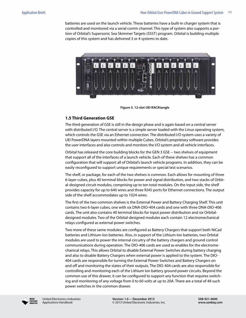
141Application Briefs How Orbital Uses PowerDNA Cubes in Ground Support System
® United Electronics IndustriesApplications Handbook
Version: 1.0 — December 2013© 2013 United Electronic Industries, Inc.
508-921-4600www.ueidaq.com
batteries are used on the launch vehicle. These batteries have a built-in charger system that is controlled and monitored via a serial comm channel. This type of system also supports a por-tion of Orbital’s Supersonic Sea Skimmer Targets (SSST) program. Orbital is building multiple copies of this system and has delivered 3 or 4 systems to date.
Figure 3. 12-slot UEI RACKtangle
1.5 Third Generation GSEThe third generation of GSE is still in the design phase and is again based on a central server with distributed I/O. The central server is a simple server loaded with the Linux operating system, which controls the GSE via an Ethernet connection. The distributed I/O system uses a variety of UEI PowerDNA layers mounted within multiple Cubes. Orbital’s proprietary software provides the user interfaces and also controls and monitors the I/O system and all vehicle interfaces.
Orbital has released the core building blocks for the GEN 3 GSE -- two shelves of equipment that support all of the interfaces of a launch vehicle. Each of these shelves has a common configuration that will support all of Orbital’s launch vehicle programs. In addition, they can be easily reconfigured to support unique requirements or special test scenarios.
The shelf, or package, for each of the two shelves is common. Each allows for mounting of three 6-layer cubes, plus 40 terminal blocks for power and signal distribution, and two stacks of Orbit-al-designed circuit modules, comprising up to ten total modules. On the input side, the shelf provides capacity for up to 640 wires and three RJ45 ports for Ethernet connections. The output side of the shelf accommodates up to 1024 wires.
The first of the two common shelves is the External Power and Battery Charging Shelf. This unit contains two 6-layer cubes, one with six DNA-DIO-404 cards and one with three DNA-DIO-406 cards. The unit also contains 40 terminal blocks for input power distribution and six Orbital-designed modules. Two of the Orbital-designed modules each contain 12 electromechanical relays configured as external power switches.
Two more of these same modules are configured as Battery Chargers that support both NiCad batteries and Lithium-Ion batteries. Also, in support of the Lithium-Ion batteries, two Orbital modules are used to power the internal circuitry of the battery chargers and ground control communications during operation. The DIO-406 cards are used as enables for the electrome-chanical relays. This allows Orbital to disable External Power Switches during battery charging and also to disable Battery Chargers when external power is applied to the system. The DIO-404 cards are responsible for turning the External Power Switches and Battery Chargers on and off and monitoring the states of their outputs. The DIO-404 cards are also responsible for controlling and monitoring each of the Lithium Ion battery ground power circuits. Beyond the common use of this drawer, it can be configured to support any function that requires switch-ing and monitoring of any voltage from 0 to 60 volts at up to 20A. There are a total of 48 such power switches in the common drawer.
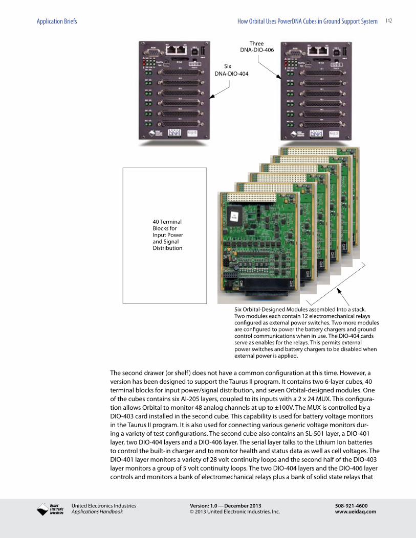
142Application Briefs How Orbital Uses PowerDNA Cubes in Ground Support System
® United Electronics IndustriesApplications Handbook
Version: 1.0 — December 2013© 2013 United Electronic Industries, Inc.
508-921-4600www.ueidaq.com
Six
DNA-DIO-406
DNA-DIO-404
Three
Six Orbital-Designed Modules assembled Into a stack. Two modules each contain 12 electromechanical relays
40 TerminalBlocks forInput Power
Distribution
con�gured as external power switches. Two more modulesare con�gured to power the battery chargers and ground
control communications when in use. The DIO-404 cards serve as enables for the relays. This permits external power switches and battery chargers to be disabled when
external power is applied.
and Signal
The second drawer (or shelf ) does not have a common configuration at this time. However, a version has been designed to support the Taurus II program. It contains two 6-layer cubes, 40 terminal blocks for input power/signal distribution, and seven Orbital-designed modules. One of the cubes contains six AI-205 layers, coupled to its inputs with a 2 x 24 MUX. This configura-tion allows Orbital to monitor 48 analog channels at up to ±100V. The MUX is controlled by a DIO-403 card installed in the second cube. This capability is used for battery voltage monitors in the Taurus II program. It is also used for connecting various generic voltage monitors dur-ing a variety of test configurations. The second cube also contains an SL-501 layer, a DIO-401 layer, two DIO-404 layers and a DIO-406 layer. The serial layer talks to the Lthium Ion batteries to control the built-in charger and to monitor health and status data as well as cell voltages. The DIO-401 layer monitors a variety of 28 volt continuity loops and the second half of the DIO-403 layer monitors a group of 5 volt continuity loops. The two DIO-404 layers and the DIO-406 layer controls and monitors a bank of electromechanical relays plus a bank of solid state relays that
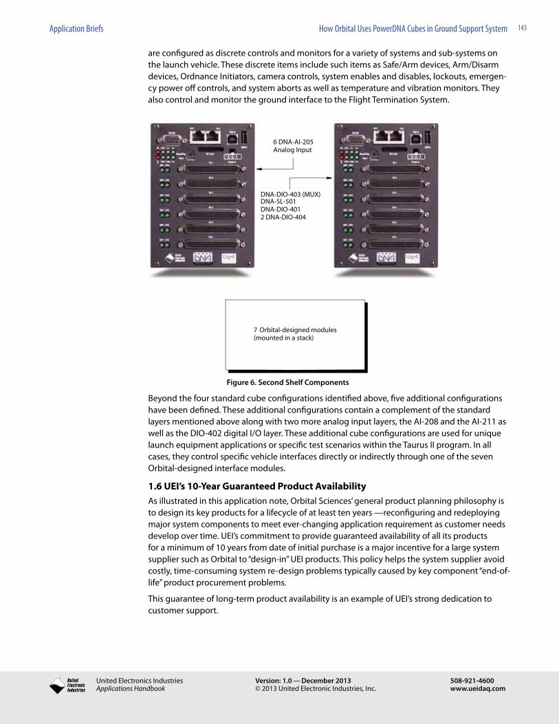
143Application Briefs How Orbital Uses PowerDNA Cubes in Ground Support System
® United Electronics IndustriesApplications Handbook
Version: 1.0 — December 2013© 2013 United Electronic Industries, Inc.
508-921-4600www.ueidaq.com
are configured as discrete controls and monitors for a variety of systems and sub-systems on the launch vehicle. These discrete items include such items as Safe/Arm devices, Arm/Disarm devices, Ordnance Initiators, camera controls, system enables and disables, lockouts, emergen-cy power off controls, and system aborts as well as temperature and vibration monitors. They also control and monitor the ground interface to the Flight Termination System.
6-layer Cube
205
501
401
6 DNA-AI-205Analog Input
DNA-DIO-403 (MUX)DNA-SL-501DNA-DIO-4012 DNA-DIO-404
7 Orbital-designed modules(mounted in a stack)
Figure 6. Second Shelf Components
Beyond the four standard cube configurations identified above, five additional configurations have been defined. These additional configurations contain a complement of the standard layers mentioned above along with two more analog input layers, the AI-208 and the AI-211 as well as the DIO-402 digital I/O layer. These additional cube configurations are used for unique launch equipment applications or specific test scenarios within the Taurus II program. In all cases, they control specific vehicle interfaces directly or indirectly through one of the seven Orbital-designed interface modules.
1.6 UEI’s 10-Year Guaranteed Product AvailabilityAs illustrated in this application note, Orbital Sciences’ general product planning philosophy is to design its key products for a lifecycle of at least ten years —reconfiguring and redeploying major system components to meet ever-changing application requirement as customer needs develop over time. UEI’s commitment to provide guaranteed availability of all its products for a minimum of 10 years from date of initial purchase is a major incentive for a large system supplier such as Orbital to “design-in” UEI products. This policy helps the system supplier avoid costly, time-consuming system re-design problems typically caused by key component “end-of-life” product procurement problems.
This guarantee of long-term product availability is an example of UEI’s strong dedication to customer support.

144Application Briefs How Orbital Uses PowerDNA Cubes in Ground Support System
® United Electronics IndustriesApplications Handbook
Version: 1.0 — December 2013© 2013 United Electronic Industries, Inc.
508-921-4600www.ueidaq.com
Background Information on Orbital and its Products
1.7 Stage 1 AssemblyThe primary function of Stage 1 is to generate the required impulse for delivering Taurus II upper stages and payloads to the target altitude, downrange and velocity conditions for stage separation. Stage 1 is also the critical structural load path for transmitting thrust forces during early ascent, and forms the primary interface between the Taurus launch vehicle and ground systems. The Stage 1 Assembly consists of the Yuzhnoye- (Ukrainian)-developed Stage 1 core structure and tanks, the AJ26-62 Main Engine System (Aerojet General MES) (Russian-developed) and Range-required Flight Termination System. The Stage 1 propulsion system uses Liquid Oxygen (LOX) and kerosene Rocket Propellant (RP)
Figure 7.. Taurus II Launch Vehicle
The LOX and RP-1 tank bays consist primarily of the propellant tanks. Both tanks have liquid lev-el sensors that are used during propellant loading and for measuring propellant levels in flight. The in-flight measurement is used by Stage 1 avionics for calculations to determine engine mixture ratio adjustments for minimizing residuals in the propellant tanks. The pressurization system supplies gas through a manifold of valves that are cycled open/closed to control propel-lant flow rate. Liquid level sensors in the LOX tank ensure that helium tanks are submerged prior to beginning the helium fill, and emergency valves protect against over-pressurization.
The aft bay contains the Main Engine System (MES), which is the primary interface between the launch vehicle and ground systems. The MES generates thrust for launch vehicle motion and control during Stage 1 ascent.The MES consists of two Aerojet General AJ26-62 LOX/RP-1 rocket engines mounted on a thrust frame with individual Thrust Vector Control (TVC) systems on each engine. The AJ26-62 engines use a sub-cooled oxygen-rich, staged combustion cycle that can be throttled from 56% to 108% and has a variable mixture ratio valve for controlling flow rates of oxidizer and fuel.

145Application Briefs How Orbital Uses PowerDNA Cubes in Ground Support System
® United Electronics IndustriesApplications Handbook
Version: 1.0 — December 2013© 2013 United Electronic Industries, Inc.
508-921-4600www.ueidaq.com
1.8 Stage 2 AssemblyStage 2 of the Taurus II contains the Stage 2 avionics module, the second stage motor and adaptor cone, the Stage 1/2 interstage, Stage 1/2 separation system, the fairing separation sys-tem, and an Attitude Control System. The avionics design uses Orbital’s latest Module Avionics Control Hardware (MACH) to provide power transfer, data acquisition, booster interfaces, and ordnance initiation. This advanced system provides communication with vehicle subsystems, Launch Support Equipment, and the payload via standard Ethernet links and UEI discrete I/O hardware. The Taurus II MACH system provides up to 3 Mbps of real-time vehicle data with dedicated bandwidth and channels reserved for payload use.
1.9 Stage 2 MotorThe baseline Taurus II uses a CASTOR Model 30A solid fuel rocket for the second stage mo-tor, built by Alliant Tech Systems, Inc. (ATK). it has a composite graphite/epoxy wound case, a mixture of TP-H8299 for its solid fuel, an ignitor and a flex seal at the throat. It generates ap-proximately 80,000 lb of thrust with an lsp of 301 seconds and a burn time of136 seconds. The motor is designed to meet the initial Taurus COTS (Commercial Orbital Transportation Services) for resupply of the International Space Station and NASA CRS (Commercial Resupply Services) mission requirements, with an extended nozzle under development for added performance for future flights.
Figure 6. CASTOR 30A Solid Rocket Motor (SRM)
1.10 Attitude Control System (ACS)The ACS provide three-axis attitude control throughout boosted flight and coast phases and uses the MES to control yaw, pitch, and roll control during Stage 1 powered flight. Stage 2 flight is controlled by the combination of the Stage TVC (thrust vector control) and onboard ACS (attitude control system) system located on the avionics ring. Attitude control is achieved using a 3-axis autopilot with PID control. Stage 1 flies an attitude profile based on trajectory optimiza-tion. Stage 2 controls parameters to achieve a target orbit insertion. Coast between Stage 1 and 2 orients the vehicle attitude for Stage 2 ignition and placement into the desired orbit. After the final boost phase, the autopilot orients the vehicle for spacecraft separation, collision and contamination avoidance, and downrange downlink maneuvers. An enhanced second stage liquid fueled engine is under development for use in 2013.
1.11 STAR 48 Third Stage OptionThe STARtm 48 third stage option uses ATK-manufactured solid rocket motors to achieve high energy orbits. These motors have extensive flight history in space applications on Delta and Shuttle rockets.
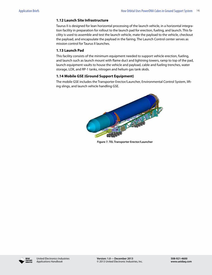
146Application Briefs How Orbital Uses PowerDNA Cubes in Ground Support System
® United Electronics IndustriesApplications Handbook
Version: 1.0 — December 2013© 2013 United Electronic Industries, Inc.
508-921-4600www.ueidaq.com
1.12 Launch Site InfrastructureTaurus II is designed for lean horizontal processing of the launch vehicle, in a horizontal integra-tion facility in preparation for rollout to the launch pad for erection, fueling, and launch. This fa-cility is used to assemble and test the launch vehicle, mate the payload to the vehicle, checkout the payload, and encapsulate the payload in the fairing. The Launch Control center serves as mission control for Taurus II launches.
1.13 Launch PadThis facility consists of the minimum equipment needed to support vehicle erection, fueling, and launch such as launch mount with flame duct and lightning towers, ramp to top of the pad, launch equipment vaults to house the vehicle and payload, cable and fueling trenches, water storage, LOX, and RP-1 tanks, nitrogen and helium gas tank skids.
1.14 Mobile GSE (Ground Support Equipment)The mobile GSE includes the Transporter Erector/Launcher, Environmental Control System, lift-ing slings, and launch vehicle handling GSE.
Figure 7. TEL Transporter Erector/Launcher

147Application Briefs PowerDNA Cubes in Bridges and StrucStructural Testing
® United Electronics IndustriesApplications Handbook
Version: 1.0 — December 2013© 2013 United Electronic Industries, Inc.
508-921-4600www.ueidaq.com
Using PowerDNA Fiber-optic Based Cubes in Bridges and Structural Testing
Bridges and tunnels are a key part of our infrastructure. Recent disasters have shown that, in
some cases, the infrastructure has degraded to such a point as to be hazardous. It has become
critical to study and determine the health of these structures, both to prevent disaster and to
lengthen the service life of the structures. The fiber-optic based (100Base-FX) DNA-FPPC5 Cube
is an ideal solution, providing the following benefits:
• Real-timemeasurementspanningover500meters
• Reducedwiringcosts90%
• Opticalfiberconnectionoffersnoise-freeEthernetconnections
• Opticalfiberinterfaceisolateshostcomputerfromlightningstrikes
• CompactsizeallowsCubeinstallationclosetosensors,thusreducingnoise
The DNA-FPPC5 Cube is a compact, rugged, 100Base-FX based DAQ interface. Its flexibility allows you to configure one or more cubes to match the specific I/O requirements of your ap-plication. The PowerDNA Cube is ideally suited for a wide variety of industrial, aerospace and laboratory data acquisition and control applications. The Fiberoptic network interface allows the cube to be located up to 2 kilometers from the host computer. A single mode fiber interface is available as a special order allowing ranges up to 20 kilometers.
PowerDNA CUBEHost PCAccelerometerUltrasonic 3D Anemometer

148Application Briefs Unmanned Land Vehicle Controller Uses UEIPAC
® United Electronics IndustriesApplications Handbook
Version: 1.0 — December 2013© 2013 United Electronic Industries, Inc.
508-921-4600www.ueidaq.com
Unmanned Land Vehicle Controller Uses UEIPACA large military operation in the development of an Unmanned Land Vehicle needed a rug-ged, low power, high density controller for the vehicle, as well as a comprehensive and flexible system to handle all of the unit’s I/O. The unit also needed to be very flexible as depending on the end application of the ULV, many different types of sensors and controls would be installed. Finally in order to preserve experience with other vehicles and to ensure fast and robust system operation, the unit must be based upon the Linux operating system.
The UEIPAC, Programmable Automation Controller was the perfect solution. It provides the environmental (tested: -40° to +85°C), and physical ruggedness (50 g shock, 5 g vibration) required and allows the installation of up to 6 I/O boards in a single 4” x 4” x 5.8” Cube. It runs a standard Linux operating system and has the ability to be easily configured with a wide variety of analog, digital, counter/timer, quadrature encoder, Serial and GPS interfaces.
The software is written on a standard Linux PC (or may be written in a Windows environment under Cygwin) using UEI’s powerful and yet simple UEIDAQ Framework. The Framework pro-vides complete support for all common versions of Linux as well as all popular Windows and Vista programming languages and applications.
The UEIPAC components used in the various systems include (depending on the end applica-tion and the sensors required):
Product Description / Usage
UEIPAC 600 6 slot, UEILogger Cube, (which includes all software)
DNA-AI-207 18-bit analog input boards are used for temperature and general voltage measurements
DNA-AO-308 8-channel analog output board provides control signals for a variety actuators and power controllers.
DNA-CT-601 8-channel counter timer boards are used as counters to moni-tor the quadrature encoder input signals.
DNA-QUAD-604 4-channel quadrature encoder input monitors the rotation of each of the ULV’s wheels.
DNA-SL-501 4-port RS-232/422/485 to interface to a variety of RS-232 devices installed in the cab as well as the DNA-GPS.
DNA-GPS High performance GPS receiver device providing < 3 meter position accuracy (using WAAS) and 0.1 mph velocity data.
DNA-DIO-404 24 point digital I/O boards are used to monitor limit switches, control relay contacts and Annunciator LEDs.

149Application Briefs Unmanned Land Vehicle Controller Uses UEIPAC
® United Electronics IndustriesApplications Handbook
Version: 1.0 — December 2013© 2013 United Electronic Industries, Inc.
508-921-4600www.ueidaq.com
ULV Controller — UEI Products Used:
UEIPAC 600The UEIPAC offers an unprecedented combination of flexibility, perfor-mance, low cost and small size. The unit is an ideal solution in a wide variety of measurement and control applications including: Temperature control, Remote vehicle control (UAV and ULV), Hardware in-the-loop (HIL) as well as embedded DAQ applications.
DNA-AI-207:18-bit analog input boards are used for temperature and general voltage measurements.
DNA-AO-308:8-channel analog output board provides control signals for a variety actuators and power controllers.
DNA-CT-601:8-channel counter timer boards are used as counters to monitor the quadrature encoder input signals.
DNA-SL-501:4-channel quadrature encoder input boards are used to monitor various rotational aspects.
DNA-QUAD-604:4-channel quadrature encoder input monitors the rotation of each of the ULV’s wheels.
DNA-GPS:High performance GPS receiver device providing < 3 meter position accuracy (using WAAS) and 0.1 mph velocity data.
DNA-DIO-404:4 point digital I/O boards are used to monitor limit switches, control relay contacts and Annunciator LEDs.

150Application Briefs Data Logging in Heavy, Off-Road Trucks
® United Electronics IndustriesApplications Handbook
Version: 1.0 — December 2013© 2013 United Electronic Industries, Inc.
508-921-4600www.ueidaq.com
Data Logging in Heavy, Off-Road TrucksApplication:A major manufacturer of industrial trucks needed to build a data logger into each vehicle in order to monitor a wide variety of systems within the vehicles. The application requires a compact, rugged, DC powered logger that could not only monitor the analog and digital inputs normally associated with data logging, but could also monitor and log information from CAN-bus devices, RS-232 interfaces and GPS position and velocity data. The logger also needs to be easily configured with different I/O configurations as many vehicles have unique I/O requirements.The UEILogger is the perfect solution. Not only does it provide the environmental (tested: -40° to +85°C), and physical ruggedness (50 g shock, 5 g vibration) required, the ability to select the I/O configuration from the wide variety of analog, digital, counter/timer, Serial, CAN and GPS interfaces ensures the logger can be configured to exactly match the require-ment of the particular vehicle. Another advantage of the UEILogger is its intuitive, easy-to-learn Windows based configuration application. As each application is somewhat different from the others, each system requires a semi-custom data logging configuration. The ease of use of the UEILogger software dramati-cally reduces the time required to train the installing technicians.Once the data logging application is competed, data may be downloaded in two ways, de-pending on the usage of the truck. Data from trucks that return to main garage is obtained by simply removing the SD card from the logger, and copying the data into a PC for further analysis and archiving. Trucks that remain in the field represented a different problem as it was prohibitively expensive to retrieve the physical SD card after each session. These vehicles were outfitted with CDMA-based high speed Cell Network interfaces. At the end of the session, the data can be downloaded by any host computer with access to the internet.
The UEILogger components used in the various systems include:
Product Description / Usage
UEILogger 600 6 slot, UEILogger Cube
DNA-AI-207 18-bit analog input boards are used for temperature and general voltage measurements
DNA-CAN-503 4-port CAN-bus interface to log data from various vehicle sen- sors and controllers.
DNA-CT-601 8-channel counter timer boards are used as counters to moni-tor the quadrature encoder input signals.
DNA-SL-501 4-port RS-232/422/485 to interface to a variety of RS-232 devices installed in the cab as well as the DNA-GPS.
DNA-GPS High performance GPS receiver device providing < 3 meter position accuracy (using WAAS) and 0.1 mph velocity data.
DNA-DIO-404 24 point digital I/O boards are used to monitor limit switches, control relay contacts and Annunciator LEDs.
Data Logging in Heavy, Off-Road Trucks — UEI Products Used:
UEILogger 600The UEILoggerTM is a powerful, flexible and easy-to-use data logger/ recorder suitable for use in a wide variety of industrial, aerospace and laboratory applications. The Log-ger contains the controller, network and SD card interface, power supply and either 3 or 6 I/O slots (UEILogger 300 or 600 respectively).

151Application Briefs Data Logging in Heavy, Off-Road Trucks
® United Electronics IndustriesApplications Handbook
Version: 1.0 — December 2013© 2013 United Electronic Industries, Inc.
508-921-4600www.ueidaq.com
DNA-AI-207:18-bit analog input boards are used for temperature and gen-eral voltage measurements.
DNA-CAN-503:4-port CAN-bus interface to log data from various vehicle sensors and controllers.
DNA-CT-601:8-channel counter timer boards are used as counters to monitor the quadrature encoder input signals.
DNA-SL-501:4-channel quadrature encoder input boards are used to monitor various rotational aspects.
DNA-GPS:High performance GPS re-ceiver device providing < 3 meter position accuracy (using WAAS) and 0.1 mph velocity data
DNA-DIO-401:24 point digital input boards are used to monitor limit switches and relay contact states.
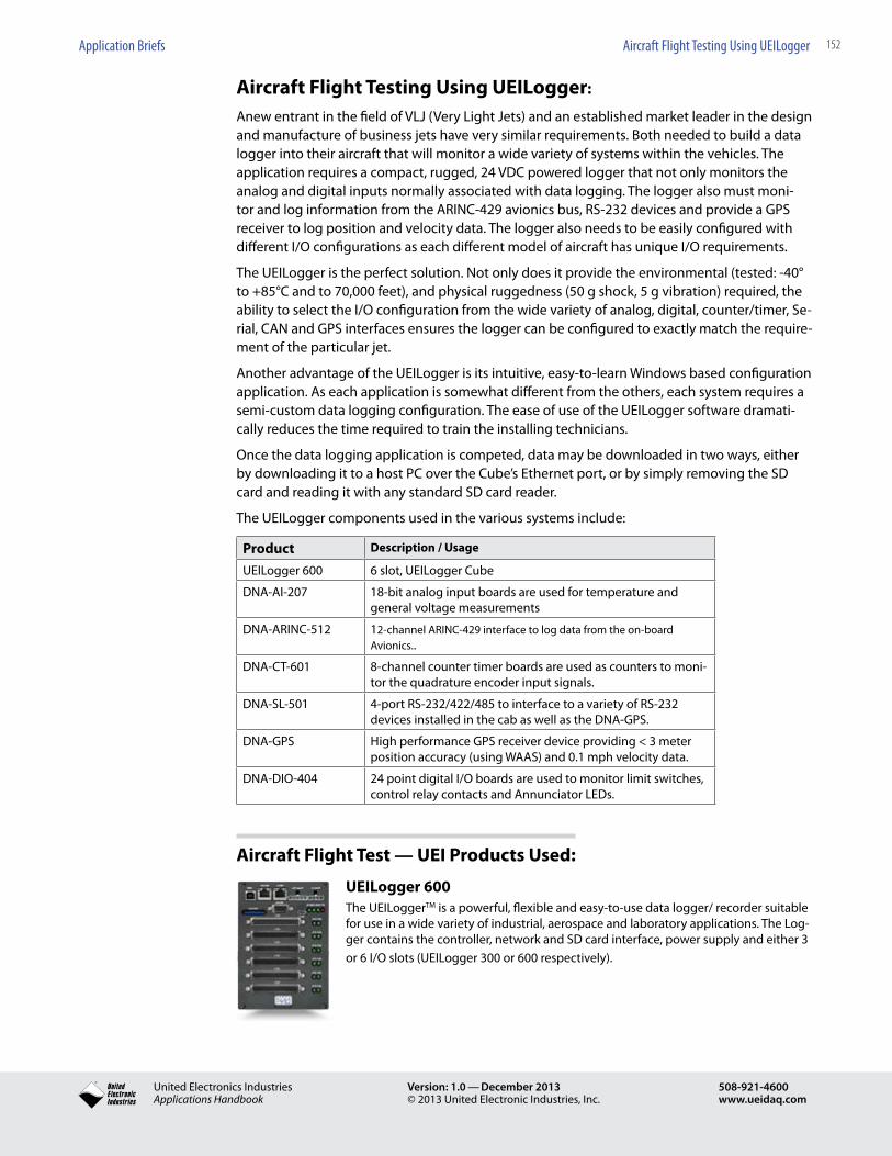
152Application Briefs Aircraft Flight Testing Using UEILogger
® United Electronics IndustriesApplications Handbook
Version: 1.0 — December 2013© 2013 United Electronic Industries, Inc.
508-921-4600www.ueidaq.com
Aircraft Flight Testing Using UEILogger:
Anew entrant in the field of VLJ (Very Light Jets) and an established market leader in the design and manufacture of business jets have very similar requirements. Both needed to build a data logger into their aircraft that will monitor a wide variety of systems within the vehicles. The application requires a compact, rugged, 24 VDC powered logger that not only monitors the analog and digital inputs normally associated with data logging. The logger also must moni-tor and log information from the ARINC-429 avionics bus, RS-232 devices and provide a GPS receiver to log position and velocity data. The logger also needs to be easily configured with different I/O configurations as each different model of aircraft has unique I/O requirements.
The UEILogger is the perfect solution. Not only does it provide the environmental (tested: -40° to +85°C and to 70,000 feet), and physical ruggedness (50 g shock, 5 g vibration) required, the ability to select the I/O configuration from the wide variety of analog, digital, counter/timer, Se-rial, CAN and GPS interfaces ensures the logger can be configured to exactly match the require-ment of the particular jet.
Another advantage of the UEILogger is its intuitive, easy-to-learn Windows based configuration application. As each application is somewhat different from the others, each system requires a semi-custom data logging configuration. The ease of use of the UEILogger software dramati-cally reduces the time required to train the installing technicians.
Once the data logging application is competed, data may be downloaded in two ways, either by downloading it to a host PC over the Cube’s Ethernet port, or by simply removing the SD card and reading it with any standard SD card reader.
The UEILogger components used in the various systems include:
Product Description / Usage
UEILogger 600 6 slot, UEILogger Cube
DNA-AI-207 18-bit analog input boards are used for temperature and general voltage measurements
DNA-ARINC-512 12-channel ARINC-429 interface to log data from the on-board Avionics..
DNA-CT-601 8-channel counter timer boards are used as counters to moni-tor the quadrature encoder input signals.
DNA-SL-501 4-port RS-232/422/485 to interface to a variety of RS-232 devices installed in the cab as well as the DNA-GPS.
DNA-GPS High performance GPS receiver device providing < 3 meter position accuracy (using WAAS) and 0.1 mph velocity data.
DNA-DIO-404 24 point digital I/O boards are used to monitor limit switches, control relay contacts and Annunciator LEDs.
Aircraft Flight Test — UEI Products Used:
UEILogger 600The UEILoggerTM is a powerful, flexible and easy-to-use data logger/ recorder suitable for use in a wide variety of industrial, aerospace and laboratory applications. The Log-ger contains the controller, network and SD card interface, power supply and either 3 or 6 I/O slots (UEILogger 300 or 600 respectively).
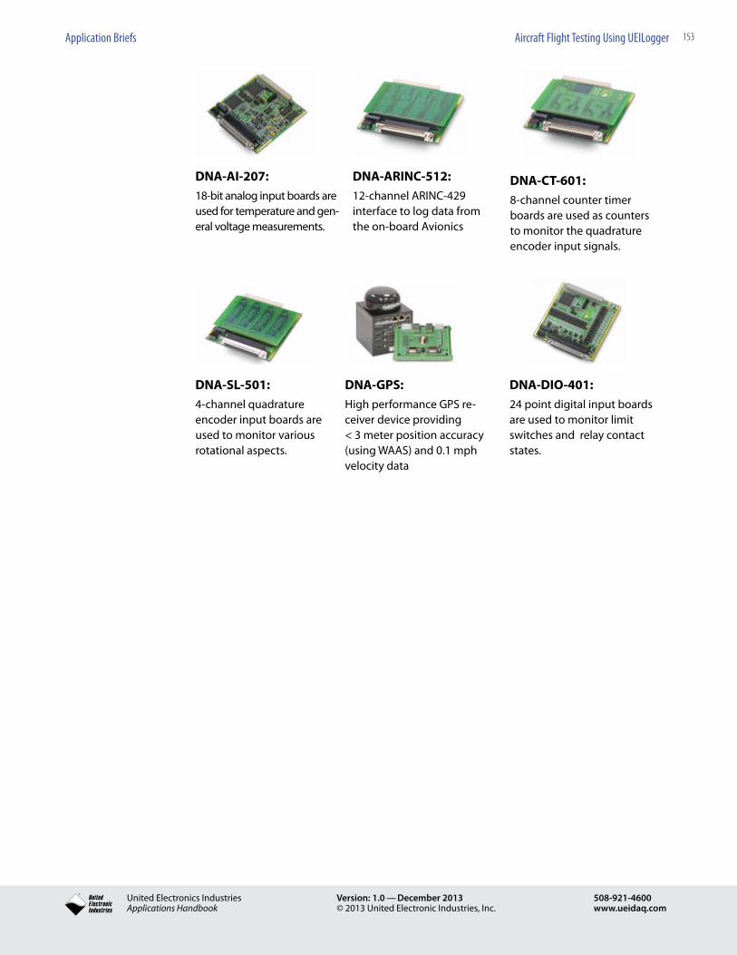
153Application Briefs Aircraft Flight Testing Using UEILogger
® United Electronics IndustriesApplications Handbook
Version: 1.0 — December 2013© 2013 United Electronic Industries, Inc.
508-921-4600www.ueidaq.com
DNA-AI-207:18-bit analog input boards are used for temperature and gen-eral voltage measurements.
DNA-ARINC-512:12-channel ARINC-429 interface to log data from the on-board Avionics
DNA-CT-601:8-channel counter timer boards are used as counters to monitor the quadrature encoder input signals.
DNA-SL-501:4-channel quadrature encoder input boards are used to monitor various rotational aspects.
DNA-GPS:High performance GPS re-ceiver device providing < 3 meter position accuracy (using WAAS) and 0.1 mph velocity data
DNA-DIO-401:24 point digital input boards are used to monitor limit switches and relay contact states.

154Application Briefs Dynamometer Automation Made Easy
® United Electronics IndustriesApplications Handbook
Version: 1.0 — December 2013© 2013 United Electronic Industries, Inc.
508-921-4600www.ueidaq.com
Dynamometer Automation Made EasyA major manufacturer of dynamometers has standardized on the PowerDNA cube as the I/O system used to monitor and control their large dynos. The dynamometers are sold to customers worldwide and are used in a wide variety of automotive, aircraft and railroad applications test-ing both engine performance as well as brake performance.
Previous systems had been based on shipping a dynamometer to the customer site in two pieces, the mechanical “machine” and the control racks. Company installation technicians then placed the dyno and the control racks in place and went through the tedious and time consum-ing task of connecting the hundreds of control and monitoring wires between the control rack and the dynamometer.
The PowerDNA’s combination of high density I/O, combined with its environmental ruggedness allows the entire I/O system to be mounted directly on the dynamometer. In the new configu-ration, when the units are installed at a customer facility, the dyno is installed and the host computer is placed in the control room. The field technicians then need only connect power, and Ethernet to the dynamometer.
The application was developed in C, and run on standard Windows operating systems. The PowerDNA products used in a typical system include:
Product Description / Usage
DNA-PPC8 6 slot, PowerDNA Cube
DNA-AI-207 18-bit analog input boards are used for temperature and general voltage measurements
DNA-AI-201-100 16-bit, 100 ksample/second analog input boards are used for high speed analog inputs
DNA-CT-601 8-channel counter timer boards are used as counters to monitor the quadrature encoder input signals.
DNA-QUAD-604 4-channel quadrature encoder input boards are used to monitor various rotational aspects.
DNA-AO-308 16-bit analog output boards are used to control various actuators
DNA-DIO-404 24 point digital I/O boards are used to monitor limit switches, control relay contacts and Annunciator LEDs.
Dynamometer Automation — UEI Products Used:
DNA-PPC8The PowerDNA® (Distributed Networked Automation) Cube is a compact,rugged, Ethernet based DAQ interface. Its flexibility allows you to configure one or more cubes to match the specific I/O requirements of your application.

155Application Briefs Dynamometer Automation Made Easy
® United Electronics IndustriesApplications Handbook
Version: 1.0 — December 2013© 2013 United Electronic Industries, Inc.
508-921-4600www.ueidaq.com
Appliance Maker Automates Temperature Measurement Test StandA major appliance manufacturer needed to automate the measurement of temperature in an oven test stand. This sounds like a very simple system, and conceptually it is. However, the system requires monitoring over 1700 thermocouples. The current, manual method of monitor-ing the temperature requires up to four technicians monitoring a bank of digital panel meters and making manual entries into a test log. This is inefficient, error prone and makes it difficult to prepare the data for presentation, analysis and archiving.
Using the PowerDNA DNA-PPC8 Cubes in conjunction with the DNA-AI-207 analog input board, the system is completely implemented in 18 Cubes. The Cubes are distributed around the test chamber, minimizing the length of thermocouple wire required. The built-in single port Ether-net switch provides in the PowerDNA Cube allows the Ethernet to be daisy chained from one cube to the next. This means the entire system may be implemented using a single Ethernet port on the host computer.
Software for this particular system was written using the UEIDAQ Framework. The Framework provides a powerful, yet simple set of drivers that may be called from all popular programming languages and applications packages (e.g. LabVIEW, MATLAB) and supports not only Windows/Vista, but also Linux and most popular Real-Time operating systems including QNX, RTX and XPC.
The system required to monitor and log 1728 thermocouples is shown below:
Product Description / Usage
DNA-PPC8 6 slot, PowerDNA Cube
DNA-AI-207 18-bit analog input boards are used for temperature and general voltage measurements
DNA-CBL-37S 8-channel counter timer boards are used as counters to monitor the quadrature encoder input signals.
DNA-STP-207TC Screw Terminal Panel provides interconnection to the TCs as well as a Cold Junction temperature sensor mounted in a large isothermal block.
Environmental / CSA Test Stand Automation — UEI Products Used:
DNA-PPC8The PowerDNA® (Distributed Networked Automation) Cube is a compact,rugged, Ethernet based DAQ interface. Its flexibility allows you to configure one or more cubes to match the specific I/O requirements of your application.

156Application Briefs Dynamometer Automation Made Easy
® United Electronics IndustriesApplications Handbook
Version: 1.0 — December 2013© 2013 United Electronic Industries, Inc.
508-921-4600www.ueidaq.com
DNA-AI-207:18-bit analog input boards are used for temperature and gen-eral voltage measurements.
DNA-CBL-37S:3ft, 37-way round shielded cable with thumb screws
a
DNA-STP-207TC:Screw Terminal Panel pro-vides interconnection to the TCs as well as a Cold Junction temperature sensor mounted in a large isothermal block.

157Application Briefs Landing Gear Strain Measurement for Mars Landing Vehicle
® United Electronics IndustriesApplications Handbook
Version: 1.0 — December 2013© 2013 United Electronic Industries, Inc.
508-921-4600www.ueidaq.com
Landing Gear Strain Measurement for Mars Landing VehicleA large NASA funded research facility needed a way to test the strength and stability of a land-ing “gear” designed for use in a future Mars landing vehicle. A prototype of the landing gear was developed and was to be subject to “drop” tests designed to simulate the stress profile of an actual landing.s
The engineers challenge was to find a system that could sample 90 strain gage inputs (simul-taneously) as well as acquire data from accelerometers, rate gyros and quadrature encoders and was: 1) light enough to not compromise the simulated crafts weight or balance, 2) rugged enough to survive 30 g landing forces and 3) could be wired to a host computer with wires light and flexible enough wires not to impact the drop dyanamics.
The DNA-PPC8 PowerDNA cube with its 6 I/O slots fit the bill perfectly. Using the 25-channel DNA-AI-225 all 96 analog input channels could be handled with four I/O boards, leaving one slot for the DNA-CT-601 counter board for quadrature encoder inputs and on free slot. This means the entire DAQ system fit in a single 4” x 4” x 5.8” cube weighing under four pounds. The PowerDNA Cube’s 50 g shock and 5 g vibration specifications also were up to the task. Finally, the Cube’s wide 9-36 VDC power requirement meant the system could draw power from batter-ies already on the simulator, leaving only a simple Ethernet cable required to connect the DAQ system to the host PC.
The application was developed in LabVIEW RT, and run on standard desktop computer. The PowerDNA products used in the system include:
Product Description / Usage
DNA-PPC8 6 slot, PowerDNA Cube
DNA-AI-225 25-channel, 24-bit simultaneously sampling A/D cards used to monitor the strain, accelerometer and rate Gyro channels
DNA-CT-601 8-channel counter timer boards are used as counters to moni-tor the quadrature encoder input signals..
Landing Gear Strain Measurement for Mars Landing Vehicle — UEI Products Used:
DNA-PPC8The PowerDNA® (Distributed Networked Automation) Cube is a compact,rugged, Ethernet based DAQ interface. Its flexibility allows you to configure one or more cubes to match the specific I/O requirements of your application.

158Application Briefs Landing Gear Strain Measurement for Mars Landing Vehicle
® United Electronics IndustriesApplications Handbook
Version: 1.0 — December 2013© 2013 United Electronic Industries, Inc.
508-921-4600www.ueidaq.com
DNA-AI-225:True 24-bit resolution makes DNA-AI-225 offers ultra-high resolution going into the microvolt level across the full input range, with one con-verter per channel with simultaneous sampling across all 25 independent ADCs and outstand-ing linearity. Long-term gain and offset drifts, as well as drift vs. temperature ratio, make it useful in a wide range of applications.
DNA-CT-601:The DNA-CT-601 is a general-purpose counter/timer layer that provides eight in-dependent 32-bit channels, each one hav-ing overvoltage protection and optoisola-tion. They perform up/down counting in a number of flexible modes. The counters also will generate PWM outputs or monitor Quadrature encoder inputs.

159Application Briefs Using the PowerDNA UEILogger in a Cellular Wireless Network
® United Electronics IndustriesApplications Handbook
Version: 1.0 — December 2013© 2013 United Electronic Industries, Inc.
508-921-4600www.ueidaq.com
Using the PowerDNA UEILogger in a Cellular Wireless NetworkThe PowerDNA UEILogger from United Electronic Industries is a standalone, compact device that is ideally suited for a wide range of data acquisition applications. Originally de-signed for use in Ethernet hard-wired networks, it can readily be adapted for use in wireless networks, such as cellular, satellite, and local wireless systems, both mobile and stationary.For cellular network applications, United recommends the use of the JBM C120 Wireless Gateway with any of several readily available aircards, which may be automatically or manually configured. Figure 1-1 shows how a JBM Gateway can typically be used in a cel-lular wireless logger system.
t
PC
PowerDNA SensorsEthernetPort
JBM C120 Wireless Gateway
AirCard
May Be Stationary or Mobile
Internet
Broadband ConnectionCellCarrier
Company
UEILogger
Power
Figure 1-1. Cellular Wireless UEILogger System (Single or Multi-Cube)
Figure 1-2 shows the hardware used in a typical UEILogger cellular wireless system. Note that the system can be configured with multiple daisy-chained UEILogger Cubes and with multiple C120 gateways, each with multiple logger Cubes.
JBM C120 Gateway
Aircard
PowerDNA UEILogger with either 3 or 6 Layers
Figure 1-2. Cellular Wireless Data Logging System with a 6-layer PowerDNA UEILogger and a JBM C120 Gateway
Recommended Applications
160Application Briefs Using the PowerDNA UEILogger in a Cellular Wireless Network
® United Electronics IndustriesApplications Handbook
Version: 1.0 — December 2013© 2013 United Electronic Industries, Inc.
508-921-4600www.ueidaq.com
Use of a cellular wireless network is recommended when your application involves a moving data source, such as a vehicle, boat, missile, or airplane, or a stationary but rotating machine. It is also convenient when the data source is in a remote or normally inaccessible location where installa-tion of wires or fiber optic cable is either too costly, too hazardous, or too difficult.
Considerations in Using Cellular NetworksIf you decide that a cellular network makes sense for your data logging application, you must also consider the following items before making your decision:
• DoesthenetworkprovideacceptablecoveragefortheareainwhichtheGate-way will be located?
• Isthenetworksufficientlyreliablesoasnottocausedatalossorinterruptedtransmission?
• Haveyouconsideredtheconsequencesofaninterrupteddatastream?Aretherisks acceptable?
• ftheapplicationrequiresmobilityofthedatasource,isthehardwaresuitableforthe environment in which it will operate?
• Isasuitablepowersourceavailablefortheequipmentinalllocations?• Arethereanyobstructionsthatcouldinterferewithdatatransmissioninany
location where the equipment will operate?When you are satisfied that these requirements are met, you can proceed with the design of your logger system. Refer to “Setting Up a Cellular Wireless Logging System” on page 3 for the recommended procedure to configure and start up such a system.
Setting Up a Cellular Wireless Logging SystemThis section describes the procedure recommended for setting up a cellular wireless data log-ger system using a PowerDNA multi-layer Logger and a JBM C120 Wireless gateway.
Use the following procedure to configure and start up the system:
STEP 1:Using the PowerDNA Cube Quick Start document, follow the instructions in the section titled “Changing the IP Address of the Cube.” Verify that the IP address of the cube is set to 192.168.100.2. Also verify that the gateway is set to 192.168.100.1 and that the netmask is set to 255.255.255.0. Be sure to enter “store” and “reset” after you make any changes, as described in the PowerDNA Cube Quick Start document.
STEP 2: Verify that you have one of the supported cellular aircards listed above. Note that the aircard must have a static IP address.
STEP 3:Using the instructions that accompanied the card, verify that the card is activated and function-ing correctly before you insert the card into the JBM Gateway.
1. Install the software that came with the aircard onto a laptop that accepts an aircard.
2. Insert the aircard into the laptop.
3. Follow the carrier-provided procedures to properly activate and unlock the card, if necessary.

161Application Briefs Using the PowerDNA UEILogger in a Cellular Wireless Network
® United Electronics IndustriesApplications Handbook
Version: 1.0 — December 2013© 2013 United Electronic Industries, Inc.
508-921-4600www.ueidaq.com
4. Using the browser on the laptop, verify that you are able to browse the Internet.
STEP 4: Before inserting the card into the JBM Gateway, resolve any signal/reception related issues with the aircard installed in the laptop.
STEP 5:Power down the laptop and remove the aircard. Gently insert the aircard into the PCMCIA slot in the JBM Gateway C120. Be sure that the aircard is firmly seated.
STEP 6: Attach the power supply connector to the C120 and connect the power supply plug to an AC power outlet.
STEP 7: Verify that the PWR (yellow) LED is lit, indicating that the unit is receiving power.
STEP 8:Connect a straight CAT-5 Ethernet cable between the Local PC (laptop) and the eth1 X connec-tor on the JBM unit. Verify that the LINK LED is lit.
STEP 9To set and verify the PC IP address, perform the following steps:
1. Go to C ontrol Panel and select “Network and Dial-up Connections.”
2. Right click on “Local Area Connection” and select “Properties.”
3. At the bottom of the “This Connection” box, double-click on “Internet Protocol(TCP/IP).”
4. Record the settings that are presently in use so that you can correctly restore the set-tings after you finish configuring your wireless connection.
5. Select “Use the following IP address” and fill in the fields with the information below:\\
• IPaddress: 192.168.1.2• SubnetMask 255.255.255.0• DefaultGateway 192.168.1.1• PreferredDNS 192.168.1.1
6. Click “OK.”
7. The previous screen will appear. Click “OK.”
8. Select Start >> Run. In the Run box, type “cmd” and click OK.
9. In the window, enter “ipconfig.” Verify that the newly entered IP address, Subnet Mask, and Default Gateway appear in the list. If they do not, it may be necessary to restart the PC to make the settings take effect.
10. Enter “exit” to end ipconfig check.
STEP 10Open a web browser and enter the following in the address bar: https://192.168.1.1:10000/.
You will receive security alerts that vary with the specific system and browser you use. Click “OK” or “Yes” to get past the alerts.
STEP 11:At the login prompt,use jbmadmin(alllowercaseletters) as the User Name and enter the

162Application Briefs Using the PowerDNA UEILogger in a Cellular Wireless Network
® United Electronics IndustriesApplications Handbook
Version: 1.0 — December 2013© 2013 United Electronic Industries, Inc.
508-921-4600www.ueidaq.com
full 6-digit serial number of the JBM C120 as the Password. This will take you to the JBM Graphical Administration Utility.
STEP 12:Ifyouhaveamanuallyconfiguredaircard,pleasecompletetheinstructionsin the Cellular Card Con-figuration section of the JBM Electronics C-120 Quick Start guide before continuing.
STEP 13: Fromthe”Configuration”tab,select”Network”ontheleftside.Scrolldownto “Ethernet Interface (eth1) Settings” and click on the “+” to expand the (eth1) settings.
At “Enter IP address,” change the address from: 192.168.1.1 to: 192.169.100.1. Click on “Save”. Do not click “Apply”, as we have more settings to change before
the new IP address takes effect.
STEP 14: Fromthe”Configuration”tab,select”Security”ontheleftside.Scrolldowntothe “Enter Port For-warding Information” section. Some of the entries in the table will already be filled in by the manufacturer. Leave them as they are. In the first two blank table entries, set the IP address to 192.168.100.2. In the first entry, enter 21 in both the In Port and Out Port columns and select “TCP”. In the second entry, enter 6334 in both the In Port and Out Port columns and then Select “UDP.” Click on “Save” only at the bottom.
STEP 15: Next, clickonthe”Management”tabandselect”Network”ontheleftside.Make note of the “Current Interface Address”. Verify that this IP address is the same as the static IP address given to you by your aircard provider. This is the IP address that you will enter into the Logger application program to access your UEILogger.
STEP 16: Click on the ”Configuration” tab and select ”Security”again. Now click on” Apply” at the bottom. This will activate the IP address change. Log back into the admin utility by entering https://192.168.100.1:10000/ into the browser address bar. Follow the same procedure that you used in Step 11 above.
STEP 17: At this point, you should be connected to the Internet through the aircard connection. Enter a URL into the browser and verify that you can access the Internet.
STEP 18: Disconnect the Ethernet cable from your local PC and connect it to the NIC In connector of your PowerDNA cube. This connects the PowerDNA cube NIC In connector to the eth1 X connector of the JBM C120
STEP19: Run your UEI Logger application from an Internet-connected computerusing the IP address obtained in Step 15.
For more information about the UEILogger and the JBM C120 cellular wireless gateway, refer to www.ueidaq.com or contact us by phone at 781-821-2890.
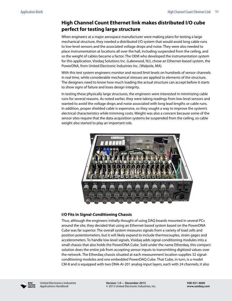
163Application Briefs High Channel Count Ethernet Link
® United Electronics IndustriesApplications Handbook
Version: 1.0 — December 2013© 2013 United Electronic Industries, Inc.
508-921-4600www.ueidaq.com
High Channel Count Ethernet link makes distributed I/O cube perfect for testing large structureWhen engineers at a major aerospace manufacturer were making plans for testing a large mechanical structure, they needed a distributed I/O system that would avoid long cable runs to low-level sensors and the associated voltage drops and noise. They were also needed to place instrumentation at locations all over the hall, including suspended from the ceiling, and so the weight of cables became a factor. The OEM who developed the instrumentation system for this application, Visidaq Solutions Inc. (Lakewood, NJ), chose an Ethernet-based system, the PowerDNA, from United Electronic Industries Inc. (Walpole, MA).
With this test system engineers monitor and record limit levels on hundreds of sensor channels in real time, while considerable mechanical stresses are applied to elements of the structure. The designers need to know how much loading the actual structure can accept before it starts to show signs of failure and loses design integrity.
In testing these physically large structures, the engineers were interested in minimizing cable runs for several reasons. As noted earlier, they were taking readings from low-level sensors and wanted to avoid the voltage drops and noise associated with long lead lengths or cable runs. In addition, proper shielded cable is expensive, so they sought a way to improve the system’s electrical characteristics while trimming costs. Weight was also a concern because some of the sensor sites require that the data-acquisition systems be suspended from the ceiling, so cable weight also started to play an important role.
I/O Fits in Signal-Conditioning ChassisThus, although the engineers initially thought of using DAQ boards mounted in several PCs around the site, they decided that using an Ethernet-based system based on the PowerDNA Cube was far superior. The overall system measures signals from a variety of load cells and position potentiometers, but it will likely expand to include thermocouples, strain gages and accelerometers. To handle low-level signals, Visidaq adds signal-conditioning modules into a small chassis that also holds the PowerDNA Cube. Sold under the name Etherdaq, this compact solution does the entire job from accepting sensor inputs to transmitting digitized values over the network. The Etherdaq chassis situated at each measurement location supplies 32 signal-conditioning modules and one embedded PowerDAQ Cube. That Cube, in turn, is a model CM-8 and is equipped with two DNA-AI-201 analog-input layers, each with 24 channels; it also

164Application Briefs High Channel Count Ethernet Link
® United Electronics IndustriesApplications Handbook
Version: 1.0 — December 2013© 2013 United Electronic Industries, Inc.
508-921-4600www.ueidaq.com
holds three DNA-DIO-403 digital-output layers with 48 points each.
A PowerDNA-based remote networked data-acquisition system with signal conditioning as designed by Visidaq Solutions, Inc.Because it measures roughly 6 x 4 x 4″ the PowerDNA Cube in the chassis takes up little space yet it holds its own CPU, network interface and still can ac-cept hundreds of analog and digital I/O channels. Using local intelligence, the Cube performs the digitization locally and sends the results to a host PC over an Ethernet network using either copper or fiberoptic cable. What made the system especially attractive for this applica-tion is its high channel count and the ability to daisychain the Cubes on one Ethernet chain. In this way, the designers could string the units along one communication line, further minimiz-ing cable runs.
In operation, four digital outputs from each one of the DNA-DIO-403 layers go to each of the 32 signal-conditioning modules. Two of the digital lines activate relays that shunt either of two precision resistors across the sensors to implement a resistance (R-Cal ) method for calibra-tion. A third digital input initiates the autozero process, which uses circuitry to compensate for voltage losses in leads and other effects. This process allows the system to zero out the voltage regardless of the sensor position and thus get a true initial condition reading of the loads or deflection. A fourth digital signal from the PowerDNA Cube allows the operator to turn sensor excitation voltage on or off.
Distributed I/O in The True SenseOnce the system has completed this calibration routine, it can begin taking measurements. The existing configuration consists of seven Etherdaq systems, each with 32 channels sam-pling at 20 Hz, located throughout a test hanger-while some are located on the floor, some are suspended in the air so they can be close to the actual sensors. Although the system uses copper cabling for the Ethernet, Visidaq Solutions could convert to the PowerDNA’s fiberoptic option if necessary.
The host software runs on a Visidaq PC-based Data Acquisition system. Because the system is recording, displaying and performing control on the signal-conditioning elements in real time, the designers chose Linux. The Visidaq Data Acquisition software is written in C because the firm started in the late 1980s using Motorola’s Unix, then ported to Data General hardware and Unix, then to Hewlett Packard and HPUX, and most recently to Linux. Although the software for this application was a custom project, Visidaq Solutions added the new features to its standard application software, which additionally provided test operators with a variety of field proven general-purpose Visidaq data acquisition functions. What makes Etherdaq unique is how implements these special signal-conditioning features. Using UEI’s PowerDNA product Visidaq Solutions could readily adapt Etherdaq for other special application requirements or remotely distribute industry standard signal conditioner products.
All referenced trademarks are the property of their respective owners.

165Application Briefs Flexible Waveform Generation Accomplishes Safe Braking
® United Electronics IndustriesApplications Handbook
Version: 1.0 — December 2013© 2013 United Electronic Industries, Inc.
508-921-4600www.ueidaq.com
Flexible Waveform Generation Accomplishes Safe BrakingJust as the antilock braking sytem (ABS) has become a critical safety feature in automotive vehicles, it perhaps is even more important in railway systems where locked wheels can result in extensive damage to both the train and the tracks.
Westinghouse Brakes (U.K.) Ltd. is a world leader in developing brakes for trains and metro sys-tems. Originally founded by George Westinghouse more than a century ago, the company now is part of the Knorr-Bremse Group. Westinghouse has developed several Wheel Slide Protection (WSP) systems, which minimize stopping distance and prevent damage to the train and the rails.
To aid in the design and testing of the WSP systems, Westinghouse Brakes engineers needed a flexible, yet affordable, way to generate arbitrary signals for a hardware-in-the-loop test system. The company turned to PCI analog output (AO) cards from United Electronic Industries (UEI) that could simultaneously generate multiple independent signals at frequencies up to 100 kHz per channel.
Different From Automobile BrakesAlthough the WSP system functions in a fashion similar to the ABS system in motor vehicles, there are some crucial differences. Both work on the same basic principle: the continuous modulation of the braking effort depending on the amount of wheel slip and adhesion condi-tions. However, in railway braking systems, the actuation is electropneumatic while an automo-tive ABS typically is electrohydraulically actuated.
Other differences deal with adhesion and stability. In automotive braking, the system must minimize any lateral movements and prevent loss of lateral stability of the vehicle, but that is less critical with a vehicle running on fixed rails. On the other hand, the amount of adhesion available to railway trains is inherently limited due to the extremely low steel-to-steel coef-ficient of friction between a train wheel and the track, and adhesion can further deteriorate in the presence of rain or foliage on the track.
A well-designed WSP system not only must minimize the stopping distance by making optimal use of available adhesion, but it also must prevent any excessive sliding of the wheels on metal rails. This sliding generates high temperatures and can lead to modifications in the chemical structure of the steel, which cause flat points on the wheel.
These deformations, in turn, produce mechanical damage to both the wheelsets and the tracks, resulting in higher running costs. For that reason, a WSP system must accurately control the amount of slip.
Controlled railway-braking systems use an electropneumatic action working in a closed loop. Such a system measures wheel speed with a tachometer mounted on each axle. Depending on the amount of slip (the relative difference between train speed and axle speed), it issues a braking command to an electropneumatic control valve with incorporated electronics, which modulates pressure in the brake cylinders. It does so in a closed loop according to a control algorithm. If any part of this feedback chain fails, the system must enter a safe state.

166Application Briefs Flexible Waveform Generation Accomplishes Safe Braking
® United Electronics IndustriesApplications Handbook
Version: 1.0 — December 2013© 2013 United Electronic Industries, Inc.
508-921-4600www.ueidaq.com
Figure 1. Simulated Braking Session
A simulated braking session is depicted in Figure 1. Three axles are shown having a controlled amount of slip relative to the ground speed while the fourth is periodically released to allow calculation of the actual train speed.
Railroad brakes have a long service life, with maintenance cycles every several years. They oper-ate in the hostile under-train location with high vibration levels and extremely variable environ-mental conditions. For these reasons, reliability, robustness, and safety are key to the design of WSP systems.
The capability to test their performance in a repeatable manner, in all possible operating condi-tions, and in the presence of failure modes is crucial to product development and safety assess-ment. But running comprehensive tests on actual trains is impractical.
Such tests not only are highly expensive, but also are not repeatable because adhesion values change continuously along the track. Further, lab testing using purposely damaged or faulty equipment would not let designers assess system performance against all possible failure modes because the number of possible electrical and mechanical faults and their combinations are high.
Testing brakes in the lab requires, among other things, very accurate simulation of the control signal that represents axle speed. On a train, this measurement is made with an axle-mounted toothed geared wheel, called a phonic wheel, coupled to a magnetic sensor that generates a tacho signal consisting of pulses at a frequency proportional to the rotational speed.
A host of undesired external factors can corrupt tacho signals. Among them are shock and vibra-tion, misalignments, eccentricity, wear and the loss of teeth, and electromagnetic interference.
To assess the performance and safety of products under these extreme conditions, engineers at Westinghouse Brakes developed a hardware-in-the-loop simulator dubbed Safety+ that can test brakes under both normal operating conditions and faulty conditions by injecting soft-ware-generated corrupted tacho signals.
The system consists of the WSP coupled to a software simulator that models train motion. Actual measured pressure signals go from the WSP to the simulator, which returns a software-generated tacho signal to the WSP. In this manner, the system can react to various braking

167Application Briefs Flexible Waveform Generation Accomplishes Safe Braking
® United Electronics IndustriesApplications Handbook
Version: 1.0 — December 2013© 2013 United Electronic Industries, Inc.
508-921-4600www.ueidaq.com
situations as if they were real. It records any deterioration in performance and checks results against a strict pass/fail criterion.
Simulating the Tacho SignalOne challenge in setting up this system was generating the simulated tacho signals. In an ideal world, it would be a variable-frequency rec-tangular pulse train of constant amplitude, which wouldn’t be difficult to generate with a reasonably flexible digital I/O card with timing-sequencing features. However, the real feedback signal differs in many respects, and it actually resembles an arbitrary analog waveform. Specifically, the engineers had to augment a pure square wave to obtain corrupted signals to simulate the following conditions:
• Electricalinterference.• Power-supplyvariations.• Toothbrokenoffthephonicwheeloraneccentricityinitsshape.• Mechanicalvibrations.• Electromagneticinterference.
Failure of the control electronics or damage in the tacho’s magnetic circuit. In some circum-stances, the tacho’s output frequency can jump by a factor of 0.5x, 2x, or 3x, and the control system must detect such a jump and switch to the actual frequency.
To generate signals that realistically emulate all possible mechanical and electrical fault condi-tions, the design team used a variety of signal-processing techniques. The resulting analog waveform is quite complex.
Being able to generate a high-resolution waveform with a range from near DC to greater than 20 kHz is beyond the capabilities of most AO cards. However, a product that could meet these specifications was UEI’s PD2-AO-8/16. The test set generates four continuously variable-frequency/variable-amplitude square waves, representing the corrupted tacho signals, one corresponding to each axle in a train car.
The most difficult part of the project was writing software to simulate the many possible error conditions that could be part of the tacho feedback signal. Each error modifies the software-generated pulse train in a subtle, yet critical, fashion, and the engineers had to duplicate these effects in software. They did so using special drivers that UEI supplied for its AO board.
That card’s onboard DSP proved crucial in solving the application requirements. Specifically, the AO modes on the card can stream data from a large datafile through the D/A converters and supply data from the DSP’s onboard memory in a circular fashion without host intervention. When changing datasets, though, a very slight gap of perhaps a few samples can appear in the datastream.
Westinghouse Brakes, on the other hand, needed a continuous stream of data, but this data consisted of a large number of small waveform segments. Further, the simulated tacho feed-back signal could not have any artificial gaps or delays that the control system might construe as false failure modes and try to react accordingly.
To solve this problem, UEI’s engineers developed a way to replace part of the data and a pointer within the DSP memory while the remainder of the memory was providing output data—and do so without disrupting the output signal in any way. They also provided a specialized driver to support this new feature and supplied a C example for this specialized direct DSP control output mode.
Although each AO card features eight independent 16-b analog outputs, the designers chose to use one output from one card for each axle. This requirement arose because WSP needed a separate clock for each D/A converter, and like almost all multichannel AO cards, this one uses a global clock for all the converters.

168Application Briefs Flexible Waveform Generation Accomplishes Safe Braking
® United Electronics IndustriesApplications Handbook
Version: 1.0 — December 2013© 2013 United Electronic Industries, Inc.
508-921-4600www.ueidaq.com
One test of the WSP takes only several minutes, but a complete test suite encompasses many hours. This is because a complete test must take into account the interactions of many vari-ables: whether the train is loaded or unloaded, different track-adhesion profiles such as dry or wet rails, the initial speed before braking, and the type of noise (white noise, jitter, or amplitude modulation of the tacho signal from different axles). Checking various combinations of these factors can lead to several hundred tests within a complete suite.
The software runs through the suite automatically, and at the end, the Westinghouse Brakes engineers can provide a spreadsheet summarizing all the pass/fail results to the customer. Only when the WSP equipment has proven itself is it awarded the Safety+ logo and approved for release to the customer.About the Author
Emanuele Guglielmino, Ph.D., holds an M.S. in electrical engineering from the University of Genoa and a doctorate in fluid power systems and control from the University of Bath. He worked for Westinghouse Brakes Ltd. as a control engineer on railway brake systems and most recently joined GE Energy in Florence, Italy. Dr. Guglielmino has authored more than 15 publications in the fields of robust control and fluid power and, in 2001,wontheASMEBestPaperAwardintheFluidPowerSystemsandTechnologyDivision.e-mail:[email protected]

169Application Briefs Data-Acquisition Drivers for Real-Time OS in Ocean-Fishery Management
® United Electronics IndustriesApplications Handbook
Version: 1.0 — December 2013© 2013 United Electronic Industries, Inc.
508-921-4600www.ueidaq.com
Data-Acquisition Drivers for Real-Time OS Ease Research into Ocean-Fishery ManagementMany technical applications simply can’t tolerate the instability and data-throughput hiccups to which Windows is prone. But when engineers try to design a system around an alternate OS, they often find that the selection of peripherals with drivers is very limited. This problem is es-pecially acute for specialized products such as data-acq cards, where overall market size makes it uninteresting for most manufacturers to take the trouble to develop drivers for anything other than Windows, knowing that with Windows alone they’ll capture the largest portion of the customer base. A few suppliers, such as United Electronic Industries (www.ueidaq.com), do care about such users and thus offer a broad range of OS support.
That’s the experience of Jim Wilson, an electronics engineer at the Environmental Technology Laboratory at the National Oceanic and Atmospheric Administration (NOAA) in Boulder, CO. When setting up a PC-based system for measuring fishery stocks in the oceans, he insisted on the reliability and realtime capabilities of the QNX operating system. For some plug-in I/O cards he found it necessary to write his own QNX drivers, but the fact that UEI supplies professionally developed QNX drivers for its PowerDAQ line of I/O hardware made those cards an easy choice.
Fish spotting with lasersFirst, though, take a quick overview of Jim’s project. Federal regulation of the offshore fish-ing industry has once again become national news, but unfortunately legislators often must make far-reaching decisions without the benefit of detailed information. When scientists try to determine how many fish of a given type are in a specific region, they typically rely on direct sampling, egg sampling, sonar (echo-sounding) surveys or aerial surveys. The surface-based techniques take considerable time and are expensive to conduct. And while aerial surveys can cover a larger area, the resulting data is generally less reliable.
That was the situation until Jim’s group at NOAA started to take a concept developed for mili-tary applications and apply it to fishery surveys. The core of the system is LIDAR (Light Detec-tion and Ranging), which operates in a fashion similar to RADAR except it uses an industrially safe laser instead of radio waves. One reason the laser is so useful is that approximately 96% of its incident optical power survives a round-trip propagation through an air/water interface and light is fast enough to make the round trip from aircraft to fish and back again before the air-craft position has changed significantly. Given this performance it’s practical to operate LIDAR from a light aircraft moving as fast as 100 m/sec. Seawater, however, rapidly attenuates light signals, so the technique is limited to measurements of fish in the upper ocean layers only as deep as 50m. Thus the system works best on upper-ocean fish types such as anchovy, sardine, mackerel and herring. Nonetheless, a typical survey flight can cover hundreds of kilometers in just a few hours. The cost, measured per survey kilometer is less than 10% of that for a ship survey, and the depth penetration is more than three times that of a visual survey.
Because the total equipment weighs only 150 kg, it’s suitable for installation into a small aircraft as long as the plane can supply at least 1.5 kW to power the experiment. The complete system consists of three major sections. The first is the laser along with its associated beam-control optics. The LIDAR employs a green laser (doubled Nd:YAG, 532-nm) to generate 12-nsec pulses and emits them at a rate of 30 pulses/sec. The linearly polarized beam gets diverged with a lens to produce a swath that varies in size with daytime or nighttime operation.
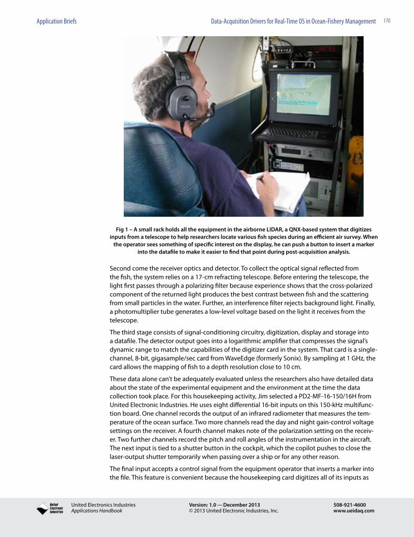
170Application Briefs Data-Acquisition Drivers for Real-Time OS in Ocean-Fishery Management
® United Electronics IndustriesApplications Handbook
Version: 1.0 — December 2013© 2013 United Electronic Industries, Inc.
508-921-4600www.ueidaq.com
Fig 1 – A small rack holds all the equipment in the airborne LIDAR, a QNX-based system that digitizes inputs from a telescope to help researchers locate various fish species during an efficient air survey. When
the operator sees something of specific interest on the display, he can push a button to insert a marker into the datafile to make it easier to find that point during post-acquisition analysis.
Second come the receiver optics and detector. To collect the optical signal reflected from the fish, the system relies on a 17-cm refracting telescope. Before entering the telescope, the light first passes through a polarizing filter because experience shows that the cross-polarized component of the returned light produces the best contrast between fish and the scattering from small particles in the water. Further, an interference filter rejects background light. Finally, a photomultiplier tube generates a low-level voltage based on the light it receives from the telescope.
The third stage consists of signal-conditioning circuitry, digitization, display and storage into a datafile. The detector output goes into a logarithmic amplifier that compresses the signal’s dynamic range to match the capabilities of the digitizer card in the system. That card is a single-channel, 8-bit, gigasample/sec card from WaveEdge (formerly Sonix). By sampling at 1 GHz, the card allows the mapping of fish to a depth resolution close to 10 cm.
These data alone can’t be adequately evaluated unless the researchers also have detailed data about the state of the experimental equipment and the environment at the time the data collection took place. For this housekeeping activity, Jim selected a PD2-MF-16-150/16H from United Electronic Industries. He uses eight differential 16-bit inputs on this 150-kHz multifunc-tion board. One channel records the output of an infrared radiometer that measures the tem-perature of the ocean surface. Two more channels read the day and night gain-control voltage settings on the receiver. A fourth channel makes note of the polarization setting on the receiv-er. Two further channels record the pitch and roll angles of the instrumentation in the aircraft. The next input is tied to a shutter button in the cockpit, which the copilot pushes to close the laser-output shutter temporarily when passing over a ship or for any other reason.
The final input accepts a control signal from the equipment operator that inserts a marker into the file. This feature is convenient because the housekeeping card digitizes all of its inputs as
171Application Briefs Data-Acquisition Drivers for Real-Time OS in Ocean-Fishery Management
® United Electronics IndustriesApplications Handbook
Version: 1.0 — December 2013© 2013 United Electronic Industries, Inc.
508-921-4600www.ueidaq.com
fast as possible running the 150-kHz A/D at its peak rate, and it makes 30 such scans every sec-ond. The system then combines this status information with the raw data from the LIDAR and saves it in one file. A typical file that consists of 2000 “shots” of the ocean takes up 2.4 M byte. This large amount of data can make it difficult to sift through to find events of particular inter-est. Thus, as the instrument’s operator monitors system activity in real time on a PC screen, he watches for interesting events. When one arises, he can push a button to insert a special marker in the datafile to allow the person performing post-experiment analysis to go to that particular spot in the datafile.
The hunt for driversClearly, requirements on the housekeeping A/D card aren’t terribly severe and any number of cards could handle the job. The problem was, though, finding cards with the necessary driver support. “I started developing this system roughly eight years ago on a 386-based machine,” Jim recalls. “Given all the tasks the system must perform without any hesitation, there was abso-lutely no processing power to spare. And because Windows could sometimes eat up CPU cycles just a brief moment before it could move on to a critical task, that situation was unacceptable for the application. That’s why we had to go to a realtime operating system, and I chose QNX 4.x”
Now he had to get the peripherals running under QNX, and fortunately in this setup the only nonstandard peripherals consisted of the two data-acq cards. For the WaveEdge board he had to adapt an existing DOS driver written in C. Although that project took him only an afternoon, it’s not the same as having a tested, verified driver from the hardware supplier on hand. Jim had looked at other vendors of gigahertz cards and notes that some of them support QNX unof-ficially. “They say, ‘Well, here’s a driver that worked for some other guys, and maybe it’ll work for you – give it a try!’ I’m looking for a higher level of support.”
Jim also relates that his original configuration for the housekeeping portion of the system used a card from Data Translation. That firm likewise had no QNX drivers, and it turned out that the card was a bit expensive and overkill for the intended tasks. When he started searching for alternatives, he looked for a data-acq vendor with QNX support and found UEI. Further, he’s completely satisfied with a cost-effective card in the PowerDAQ family, which handles all the tasks he requires at a price that fits in his budget.
System development with the PowerDAQ card proceeded smoothly, although Jim feels that he would have liked more-detailed documentation about the card and the software. However, he adds, a few quick calls to tech support solved the few minor questions that arose. The only snag came when he found a bug in the QNX driver, one that he discovered as being among the first users of the driver. It was a problem that tech support solved very easily: in one of the .H setup files a line had an incorrect variable value which inadvertently got transposed from a 0 to a 1. Once that was corrected (and was immediately fixed on the general release of the QNX driver), the card worked fine.
As he enhances the system and wants to add other peripherals beyond the two DAQ cards, he is considering a switch to another OS, possibly even Windows. “We wanted multiple serial ports, but you don’t just walk down to the local computer store and pick up a multiport serial board with QNX drivers off the shelf.” His search did ultimately lead him to a RocketPort card from Comtrol, a firm that does support QNX. One of the major problems Jim faces now is that hardware is continually being developed that he would like to add to the LIDAR system, such as a CD burner. The problem stems from the fact that QNX has moved on to QNX 6.0 and the developer isn’t supporting version 4.x any more. “We have a big decision to make,” Jim reflects, “we need to either port everything over to QNX 6.0 or find a new OS”.
And in the years since he first designed the system architecture, PCs have become tremendous-ly more powerful in terms of computational ability, video display, bus speeds and transfer rates.

172Application Briefs Data-Acquisition Drivers for Real-Time OS in Ocean-Fishery Management
® United Electronics IndustriesApplications Handbook
Version: 1.0 — December 2013© 2013 United Electronic Industries, Inc.
508-921-4600www.ueidaq.com
“Because of this power, we don’t have to pay as much attention to the realtime aspects as we did with hardware from just a few years ago,” notes Jim. Even so, he plans to stick with UEI for data acquisition because of the experience he got from the firm’s support department and the bang for the buck. He only wishes they had a gigahertz sampling card.
Algorithms being refinedJim’s group is also working on the software side. LIDAR has been in use for more than 30 years in oceanic environments, but it’s only been in the last decade that advances in signal-process-ing algorithms and calibration experiments made it worthwhile to perform a detailed analysis of incoming data. However, much work is still required in algorithms to convert LIDAR data into quantitative information about stock abundance, species and size.
Fig 2 – A typical screen shot from an aerial survey shows only that there is a fair amount of plankton in this region. The X number is the Shot Number, and the Y axis represents depth. Water surface is 0m, so
the range here is 5m above the surface to 50m below the surface. White means no signal returned, while cool colors represents a low signal, increasing to reds for higher signals. In this case, the violet layer
between 5m and 10m shows a light layer of plankton, the darker blue sections show a denser plankton concentration. The blue below approximately 30m is noise due to a large amount of glacial silt in the
Alaskan waters where this shot was taken.
For instance, today the system can’t distinguish between a single large fish or a school of small fish. However, with the support of the ship sampling crews, researchers can make a reasonably good estimate of the type and density of the fish by combining both LIDAR data and surface-ship observations. Researchers must consider other clues available such as the habitat being surveyed, in particular the water column and latitude, time of year and the types of fish sam-pled by the ships. The researchers are also discovering algorithms and techniques that allow them to use characteristics of the return signal such as its strength, polarization and frequency spectrum to provide even more information about the size, density and possibly even the spe-cies of the fish being observed.
For more information on Fish LIDAR, contact the NOAA/ETL web site at http://www.etl.noaa.gov/technology/instruments/floe/

173Application Briefs Digital I/O Card Counts DNA Fragments in Nano Biotechnology System
® United Electronics IndustriesApplications Handbook
Version: 1.0 — December 2013© 2013 United Electronic Industries, Inc.
508-921-4600www.ueidaq.com
Digital I/O Card Counts DNA Fragments in Nano Biotechnology System Many processes use a sieve to sort physical objects for counting and analysis, but what do you do at the molecular level. How can you set up a system that works with resolutions so tight that they pass only fragments of a DNA molecule, one at a time?
Figure 1
The system setup is shown in Figure 1. Labeled DNA fragments pass through the illumination volume in single file, and an optical detector reacts to the photons each sample gives off. A digital-input subsystem keeps track of the number of photons, and a PC analyses and displays the results.Not only is the physical sorting a challenge, the related electronics are, as well. It’s not enough to run a digital-input counting subsystem at a high speed; the associated counters must be large enough so they don’t overrun too quickly, and such a card must be able to move megabytes of data to a host machine without suffering from even the tiniest gap in the data. Those were some of the key requirements of Warren Zipfel, assistant director of the NIH-funded Developmental Resource for Biological Imaging and Optoelectronics (DRBIO) at Cornell Uni-versity, who is involved in constructing the data-acquisition hardware of a new “nano-device” designed to quantify DNA fragments. In collaboration with DRBIO researchers Jonas Korlach and group director Watt Webb, and with nanofabrication experts Mathieu Foquet and Harold Craighead of Cornell’s Nanobiotechnology Center (NBTC), the group is using a combination of sophisticated silica substrates, electrophoresis, optics, and PC-based data acquisition to gather statistics on fragment sizing in DNA. When this technique is perfected, it could provide an inex-pensive and fast alternative to conventional gel electrophoresis.
One enabling technology has been the ability of the researchers to use high-end lithography techniques to create channels in silicon and glass substrates as small as a few hundred na-nometers. Devices this small provide a means of achieving an effective optical resolution not possible with traditional optical techniques in the sense that a researcher can separate, confine, and observe a single molecule in a region much smaller than the optical spot size.
These “nano-channels” are so tiny that it’s relatively easy to ensure that large molecules such as DNA pass through one at a time, and the researchers are putting this effect to good use. In their prototype system, the operator starts with a small sample of DNA that has been enzymatically cleaved into fragments of various lengths. Next, by binding fluorescent reagents onto each

174Application Briefs Digital I/O Card Counts DNA Fragments in Nano Biotechnology System
® United Electronics IndustriesApplications Handbook
Version: 1.0 — December 2013© 2013 United Electronic Industries, Inc.
508-921-4600www.ueidaq.com
fragment the scientist can label each one in a way whereby the amount of fluorescent probe per fragment increases with fragment size. Fluorescence is used routinely in labs as a sensitive way to monitor biochemical reactions and to quantify important biomolecules such as proteins or DNA.
Once the sample is loaded into the device, an electric field in the range of 100V/cm induces the fragments to flow, one by one in single file, through a 250 x 500-nm wide channel in the device. A focused laser excites the fluorescently labeled fragments so they emit flashes of light while traveling through the illuminated region in the nano-channel. Each flash of light is a single photon, which the system then detects with a photomultiplier tube or avalanche photodiode. The photodetector sends out a TTL-level pulse for each detected photon. Then a digital counter card keeps track of the number of pulses that come in quick succession, and with this informa-tion the laboratory-written acquisition and analysis software can identify a “burst”—a collection of photons that correspond to a DNA fragment passing through the laser spot.
The software then analyzes the number of bursts as well as the number of photons in each one along with each burst’s temporal width. It displays these results as a histogram and they corre-spond closely to a scan you’d get from an image resulting from gel electrophroesis—the tradi-tional method of separating and analyzing DNA samples. Note that with this system you count every molecule in the sample, whereas with the gel method it’s far more difficult to accurately quantify the amount of each DNA fragment. A further advantage is that this newer technique can work with a much smaller sample size compared to conventional electrophoresis methods.
To count the TTL pulses from the optical-detection subsystem, Zipfel chose a PD2-DIO-64CT card from United Electronic Industries. He uses the three counter/timers that come integrated in the DSP chip that controls the card’s operation; two of the counters act as timing clocks to define bin size, while the third counts incoming pulses. The DSP reads the third counter on the fly and sends the increasing count value to the host PC. The 24-bit counters are sufficiently large to handle the thousands of photon pulses per bin that might come in while a large DNA fragment passes through the illuminated spot in the channel.
Figure 2
In Figure 2, The fluid is confined to the interior of the nanochannel, therefore, only a fraction of the laser illumination causes excitation.The DIO board is capable of continuously reading the counter output at a rate of 1.0 MHz if required, providing 1-µsec resolution for determin-

175Application Briefs Digital I/O Card Counts DNA Fragments in Nano Biotechnology System
® United Electronics IndustriesApplications Handbook
Version: 1.0 — December 2013© 2013 United Electronic Industries, Inc.
508-921-4600www.ueidaq.com
ing photon burst width and time between bursts. At this datarate, gap-free acquisition for long periods can place an enormous workload on the PC, creating a problem if realtime data analysis is required. Fortunately, Zipfel knew about the special ACB (advanced circular buffer) on PowerDAQ cards, which allows them to stream large amounts of data to the host PC’s hard disk and do so gap free. Several years ago, he designed a DOS-based system that had to digitize analog inputs for lengthy periods, and he chose a previous generation of streaming hardware and software from UEI.
When he needed the same capability in a PCI digital I/O card, however, he found that the cur-rent generation from UEI didn’t offer that streaming capability for the DSP-based counters. Even so, Zipfel inquired because he felt like his request would get serious attention. “UEI is small enough that when you call into that company, they are responsive. I had queried some larger companies about this project and even visited their booths at trade shows, but they never bothered to get back to me. But not only does UEI respond right away, I was speaking with the card’s designer and the fellow who wrote the firmware. I explained what I needed, and they came back with an upgrade to the firmware command interpreter that runs on the DSP. The upgrade contained new calls into the I/O function library that allowed me to do exactly what I needed with those timers. I don’t believe I could expect this level of quick, personalized service from any other supplier.” Because the PD2-DIO board’s DSP handles the transfer of I/O data to RAM, the PC has plenty of resources available to analyze the incoming stream of photon counts in real time.
In fact, Zipfel adds that his group had spent considerable money on dedicated systems that couldn’t do the job. “So here we had a $400 digital I/O card that enabled us to complete a pro-ject, and it worked better than a specialized card that sold for $15,000,” he comments.
This system presently monitors one nanometer-sized channel on a device. With the proof of concept successfully behind them, the researchers are looking to expand the applications. For instance, they envision a system with tens or hundreds of channels that could quantify DNA fragments by size, or even sort fragments into separate storage reservoirs for later retrieval. Zipfel has several other applications for the PD2-DIO board including an inexpensive autocor-relator for a biophysical technique know as Fluorescence Correlation Spectroscopy (FCS) and to replace more expensive “multichannel scalers” he has previously used for several other types of biophysical and photophysical measurements.
176
® United Electronics IndustriesApplications Handbook
Version: 1.0 — December 2013© 2013 United Electronic Industries, Inc.
508-921-4600www.ueidaq.com
Glossary A
AA/DAnalog-to-digital.
A/D Channel List StartSignal used to start the A/D acquisition of channels in the channel list. The triggering edge of this signal (falling edge) enables the ADC Conversion Start signals.
A/D ConversionThe process of converting a single analog input to a digital value.
A/D Conversion StartSignal used to start the conversion process of an analog input to a digital value. The source of this signal can be either an internal ADC synchronous clock or an external asynchro-nous signal. This signal causes the stepping in the Channel List.
AC—Alternating CurrentElectric current that varies in amplitude and direction. The usual waveform of ac is a sine wave, but can be triangular, or square.
ADC—Analog-to-Digital Converter (a.k.a. simply an “A/D”)An electrical circuit that converts analog voltage into a binary number. A/D converters perform the measurements in all data acquisition systems.
AliasA false lower frequency image of a high-fre-quency component that appears in sampled data acquired at too low a sampling rate. For more information about aliasing please visit this explanation at Analog Devices.
AlumelA brand name for a magnetic nickel alloy containing small amounts of manganese, alu-minum, and silicon. Used in thermocouples and thermocouple extension wire.
Ampere (A)SI unit of electric current.
AmplifierA device for increasing the power of a signal by taking power from a power supply and controlling the output to match the input signal shape but with a larger amplitude.
AmplitudeThe size or magnitude of a signal.
Analog InputAn analog input is an infinitely variable signal. In most data acquisition systems this signal is connected to an input amplifier and then to an A/D converter.
Analog OutputA waveform or control signal generated as a con-tinuous function of the measured parameter.
Analog TriggerA trigger that occurs at a user-selected point on an incoming analog signal. Triggering can be set to occur at a specific level on either an increasing or a decreasing signal (positive or negative slope).
Anti-alias filterA low pass filter that allows the desired low frequency component of the input waveform through, but stops the higher frequency components that can lead to aliasing errors (See Alias).
APIApplication Programming Interface, a collec-tion of high-level language function calls that provide access the functions in a driver or other utility.
ArgumentAn Input parameter to a program.
ARINC 429An avionics interface protocol which is the standard communications link in virtually all modern commercial aircraft.
4 A Glossary of Terms Commonly Used In Data Acquisition and Control
177
® United Electronics IndustriesApplications Handbook
Version: 1.0 — December 2013© 2013 United Electronic Industries, Inc.
508-921-4600www.ueidaq.com
Glossary A–C
ASCIIAmerican Standard Code for Information Interchange Coding for text files.
AssemblerA program that translates assembly language instructions into machine language instruc-tions.
Assembly LanguageA machine oriented language in which mne-monics are used to represent each machine language instruction for a particular CPU.
ASTMAmerican Society for Testing and Materials.
Asynchronous(1) Hardware—A property of an event that occurs at an arbitrary time, without synchroni-zation to a reference clock.
(2) Software – A property of a function that begins an operation and returns prior to the completion or termination of the operation.
B-Type ThermocouplePlatinum-rhodium thermocouple with a tem-perature range of 600 to >1700 °C.
BackboneThe primary-level of a hierarchical computer network connected to lower-level nodes in the hierarchy.
Background AcquisitionBackground Data Acquisition refers to data that is acquired while another program or processing routine is running in the fore-ground without apparent interruption
Background NoiseInterfering signals that can cause disturbance affecting a signal that may distort the intend-ed signal.
Base AddressA memory address that serves as the start-ing address for programmable registers. All other addresses are located by adding to the base address.
Batch processAny process on which operations are carried out on a limited number of articles, as op-posed to continuous process.
BipolarA signal range that includes both positive and negative values (for example, -5 V to +5 V).
BitOne binary digit (either 0 or 1).
Block ModeA high-speed data transfer in which the ad-dress of the data is sent followed by a speci-fied number of back-to-back data words.
Burst ModeA high-speed data transfer in which the ad-dress of the data is sent followed by back-to-back data words while a physical signal is asserted.
BusThe group of conductors that interconnect individual circuitry in a computer. Typically, a bus is the expansion vehicle to which I/O or other devices are connected. Examples of PC buses are the ISA and PCI buses.
Bus MasterA type of a plug-in board or controller with the ability to read and write devices on the computer bus, without using the host CPU.
BByteEight related bits of data, an eight-bit binary number. Also used to denote the amount of memory required to store one byte of data. A byte may represent 256 unique numbers (typically from 0 to 255 in the decimal system)
CCacheHigh-speed processor memory that buff-ers commonly used instructions or data to increase processing throughput.
178
® United Electronics IndustriesApplications Handbook
Version: 1.0 — December 2013© 2013 United Electronic Industries, Inc.
508-921-4600www.ueidaq.com
Glossary C
CalibrationThe process of determining the relation-ship between the output of a measurement device, and the input data, and comparing it against a measurement standard. In most cases, the term calibration also includes the process of adjusting the output of the meas-urement device to comply with the measure-ment standard.
CAN (CAN-bus)Abbreviation for Controller–area network, a vehicle bus standard designed to allow mi-crocontrollers and devices communicate with one another within a vehicle without requir-ing host computer.
CapacitanceThe amount of a stored (or separated) electri-cal charge for a given electrical potential, measured in farads (F).
CEConformite Européenne. A mark designat-ing product’s compliance with all applicable European Union legal requirements.
Channel ListA variable length list of channels and their as-sociated gains specifying which analog input channels to convert to digital values. In continu-ous A/D acquisition mode, the list wraps around to the first channel after it reaches the end. The channels need not be in any particular order.
ChromelA 90% nickel alloy with about 10% chromium, used with Alumel in K-type thermocouples.
CMRRCommon-Mode Rejection Ratio. A measure of an instrument’s ability to reject interfer-ence from a common-mode signal, usually expressed in decibels (dB).
Code GeneratorA software program, controlled from an intui-tive user interface, that creates syntactically correct high-level source code in languages such as C or Basic.
Cold-Junction CompensationCompensation for ambient temperature when a thermocouple is used in a data acquisition system.
COM portA serial device connectivity port on a PC, often RS-232.
Common-Mode RangeThe input range over which a circuit can handle a common-mode signal.
Common-Mode SignalThe mathematical average voltage, relative to the computer’s ground, of the signals from a differential input. For more information on the Common-Mode Signal please visit Maxim/Dallas.
Component SoftwareAn application that contains one or more component objects that can freely interact with other component software. Examples include OLE enabled applications such as Microsoft Visual Basic and OLE Controls for virtual instrumentation in Component Works.
Control Register(s)Registers containing bits that initiate control signals for various onboard subsystems.
Conversion TimeThe time elapsed, in an analog input or output system, from the moment a channel is interrogated (such as with a read instruction) to the moment that accurate data is available.
Counter/TimerA circuit such as the Intel 8254 device that counts external pulses or clock pulses (timing).
CouplingThe manner in which a signal is connected from one location to another.
CrosstalkAn unwanted signal on one channel induced by signal activity on another nearby channel.

179
® United Electronics IndustriesApplications Handbook
Version: 1.0 — December 2013© 2013 United Electronic Industries, Inc.
508-921-4600www.ueidaq.com
Glossary C–D
Current Drive CapabilityThe amount of current a digital or analog output channel is capable of sourcing or sinking while still operating within voltage range specifications.
Current SinkingThe ability of a DAQ board to dissipate current for analog or digital output signals.
Current SourcingThe ability of a DAQ board to supply current for analog or digital output signals.
DD/ADigital-to-analog
DACDigital-to-analog converter. An integrated circuit that converts a digital number into a corresponding analog voltage or current.
DAC Conversion StartSignal used to start the conversion process of digital value to an analog output. The source of this signal can be either an internal DAC synchronous clock or an external asynchro-nous signal. This is a common signal fed to both DACs.
Data Acquisition(1) The process of automatically collecting and measuring electrical signals from sensors, transducers, and test probes or fixtures and inputting them to a computer for process-ing; (2) Collecting and measuring the same kinds of electrical signals with A/D and/or DIO boards plugged into a PC, and possibly generating control signals with D/A and/or DIO boards in the same PC.
Data LoggerA stand alone data acquisition device that acquires data and stores it in local memory from which it may then be downloaded to a computer for subsequent analysis and display.
Data RecorderAnother name for a data logger, though data recorders are typically higher performance
and offer higher sample rates than a typical data logger.
DAQAn abbreviation for Data acquisition.
dBDecibel. The unit for expressing a logarith-mic measure of the ratio of two signal levels: dB=20log10 V1/V2, for signals in volts.
Differential InputAn analog input consisting of two terminals, both of which are isolated from computer ground, whose difference is measured.
DIODigital input/output.
DLLDynamic Link Library. A software module in Microsoft Windows containing executable code and data that can be called or used by Windows applications or other DLLs. Func-tions and data in a DLL are loaded and linked at run time when they are referenced by a Windows application or other DLLs.
DMADirect memory access. A method by which data can be transferred to/from computer memory from/to a device or memory on the bus while the processor does something else. DMA is the fastest method of transferring data to/from computer memory.
DNLDifferential Non-linearity. A measure in LSB of the worst-case deviation of code widths from their ideal value of 1 LSB. For more informa-tion on Differential Non-Linearity please visit the Computer Action Team
DriversSoftware that controls a specific hardware device, such as DAQ boards.
DSPDigital Signal Processor. A specialized micro-processor for digital signal processing.
Dual-Ported MemoryMemory that can be simultaneously accessed by more than one controller or processor.
180
® United Electronics IndustriesApplications Handbook
Version: 1.0 — December 2013© 2013 United Electronic Industries, Inc.
508-921-4600www.ueidaq.com
Glossary D–G
Dynamic RangeThe ratio of the largest signal level a circuit can handle to the smallest signal level it can handle (usually taken to be the noise level), normally expressed in dB.
EEEPROMElectrically erasable programmable read-only memory. ROM that can be erased with an electrical signal and reprogrammed.
Embedded ControllerA control device built into (embedded in) a host device. Monitoring and control are handled by the same CPU as general system operation.
EncoderA device that converts linear or rotary dis-placement into digital or pulse signals. The most popular type of encoder is the optical quadrature encoder, which uses a rotating disk with alternating opaque areas, a light source, and a photo detector to indicate a rotary position.
EPROMErasable programmable read-only memory. ROM that can be erased (usually by ultraviolet light exposure) and reprogrammed.
EventsSignals or interrupts generated by a device to notify another device of an asynchronous event. The contents of events are device-dependent.
External TriggerA voltage pulse from an external source that triggers an event such as A/D conversion.
FFIFOFirst-In First-Out Memory Buffer. The first data stored is the first data sent to the acceptor.
Filter
A device that allows certain parts of a signal to pass through while blocking others. In data
acquisition systems, the most common type of filter used is a low pass, anti-aliasing filter. For more information on filters please visit this page at Texas Instruments
Fixed-PointA format for processing or storing numbers as digital integers.
Floating-PointA format for processing or storing numbers in scientific notation (digits multiplied by a power of 10).
FunctionA set of software instructions executed by a single line of code that may have input and/or output parameters, that returns a value when executed.
GGainThe factor by which a signal is amplified, sometimes expressed in dB.
Gain AccuracyA measure of deviation of the gain of an amplifier from the ideal gain.
GPIBGeneral Purpose Interface Bus. Also known as IEEE-488, the GPIB was originally developed by Hewlett Packard and called the HPIB. For more information on GPIB please visit Radio-Electronics
GPSGlobal Positioning System. A series of satellites is used to provide accurate location and velocity in-formation to both ground based and land based devices. A powerful and often ignored benefit in data acquisition applications is the ability of a GPS system to generate extremely accurate timing information. One microsecond accuracy is available with inexpensive units and much tighter specifications are available from some vendors. For more information on GPS please visit Trimble or Garmin.
GroundIn terms of data acquisition systems, a ground is typically where system current is returned.
181
® United Electronics IndustriesApplications Handbook
Version: 1.0 — December 2013© 2013 United Electronic Industries, Inc.
508-921-4600www.ueidaq.com
Glossary G–I
In single ended systems the negative terminal of the sensor is typically connected to ground.
Ground LoopMany measurements are made between an input signal and ground. However, ground is not an absolute reference point and current flowing in wires between various ground con-nections can cause the potential at different “ground” points in the system to be at differ-ent potentials. These differences then mani-fest themselves as errors in the measurement.
GUIGraphical User Interface. An intuitive, easy-to-use means of communicating information to and from a computer program by means of graphical screen displays. GUIs can resemble the front panels of instruments or other ob-jects associated with a computer program.
HHandlerA device driver that is installed as part of the operating system of the computer.
HardwareThe physical components of a computer system, such as the circuit boards, plug-in boards, chassis, enclosures, peripherals, cables, and so on.
II/OInput/Output. The transfer of data to/from a computer system involving communications channels, operator interface devices, and/or data acquisition and control interfaces.
ICP® (piezoelectric vibration sensor)A simple yet powerful 2-wire interface devel-oped by PCB Piezo Electronics® to facilitate connection of Piezo Crystal based vibration sensors to data acquisition systems. Also referred to as IEPE.
IMDIntermodulation Distortion. The ratio, in dB, of the total rms signal level of harmonic sum and difference distortion products, to the
overall rms signal level. The test signal is two sine waves added together according to the following standards:
INLIntegral Non-linearity. A measure in LSB of the worst-case deviation from the ideal A/D or D/A transfer characteristic of the analog I/O circuitry. For more information about Integral Non-linearity please visit Maxim Integrated Products
Input Bias CurrentThe current that flows into the inputs of a circuit.
Input ImpedanceThe measured resistance and capacitance between the input terminals of a circuit.
Input Offset CurrentThe difference in the input bias currents of the two inputs of an instrumentation amplifier.
Instrumentation AmplifierA circuit whose output voltage with respect to ground is proportional to the difference between the voltages at its two inputs.
Integral ControlA control action that eliminates the steady-state offset inherent in proportional control.
Integrating ADCAn ADC whose output code represents the average value of the input voltage over a given time interval.
InterpreterA software utility that executes source code from a high-level language such as Basic, C, or Pascal, by reading one line at a time and executing the specified operation.
InterruptA computer signal indicating that the CPU should suspend its current task to service a designated activity.
IPCInterprocess Communication. Protocol by which processes can pass messages. Messag-es can be either blocks of data and informa-tion packets, or instructions and requests for
182
® United Electronics IndustriesApplications Handbook
Version: 1.0 — December 2013© 2013 United Electronic Industries, Inc.
508-921-4600www.ueidaq.com
Glossary I–M
process to perform actions. A process can send messages to itself, other processes on the same machine, or processes located any-where on the network.
Isolation VoltageThe voltage that an isolated circuit can nor-mally withstand, usually specified from input to input and/or from any input to the ampli-fier output, or to the computer bus.
KkKilo, the standard metric prefix for 1,000, or 103, used with units of measure such as volts, Hertz, and meters.
K (computer)Kilo, the prefix for 1,024, or 210, used with byte in quantifying data or computer memory.
kbytes/sA unit for data transfer that means 1,000 or 103 bytes/s.
LLabVIEW™A popular data acquisition programming lan-guage developed by National Instruments.®
Layer(1) Generic term often used to refer to one of the 7 Layers of the Open Systems Inter-connection Basic Reference Model or OSI Model a layered, abstract description for communications and computer network protocol design.
(2) A term used throughout the UEI website, and literature to describe the printed circuit boards of the UEI Cubes, and the RACKtan-gle™, (ie. I/O layers, CPU/NIC layer, etc.)
LinearityThe adherence of device response to the equation R = KS, where R = response, S = stimulus, and K = a constant.
LSBLeast significant bit. In terms of data acquisi-tion and measurement systems, the LSB is the
smallest change in input that can be detected by the system’s A/D converter.
LXIDesigned as the Successor to GPIB, LXI is a standard developed by the LXI Consortium, and is an abbreviation for LAN eXtensions for Instrumentation. More information can be found at the LXI Standard Website
MM(1) mega, the standard metric prefix for 1 mil-lion or 106, when used with units of measure such as volts and Hertz;
(2) mega, the prefix for 1,048,576, or 220, when used with byte to quantify data or com-puter memory.
Mbytes/sA unit for data transfer that means 1 million or 106 bytes/s.
MMIMan-Machine Interface, also Human-Machine Interface(HMI): The means by which an opera-tor interacts with an industrial automation system; often a GUI.
ModbusA defacto standard communications pro-tocol used in a wide variety of Industrial Control and DAQ (data acquisition) systems industrial control and monitoring equip-ment. Modbus was developed by Modicon in 1979 as a means to facilitate communi-cation in their programmable controller products. For more information on Modbus, please visit Modbus-IDA.
MultitaskingA property of an operating system in which several processes can be run simultaneously.
MuxMultiplexer. A switching device with multiple in-puts that sequentially connects each of its inputs to its output, typically at high speeds, in order to measure several signals with a single analog input channel. Most data acquisition systems utilize multplexers to allow a single A/D converter to measure or monitor multiple inputs.
183
® United Electronics IndustriesApplications Handbook
Version: 1.0 — December 2013© 2013 United Electronic Industries, Inc.
508-921-4600www.ueidaq.com
Glossary N–P
NoiseAn undesirable electrical signal. Noise comes from external sources such as the AC power line, motors, generators, trans-formers, fluorescent lights, soldering irons, CRT displays, computers, electrical storms, welders, radio transmitters, and internal sources such as semiconductors, resistors, and capacitors.
Nyquist SamplingSampling based on Harry Nyquist’s Bell System Technical Journal article of 1924 often called the Nyquist-Shannon Sampling Theo-rem states, “Exact reconstruction of a contin-uous-time baseband signal from its samples is possible if the signal is bandlimited and the sampling frequency is greater than twice the signal bandwidth.” For more information on Nyquist Sampling please visit this explanation at Wikipedia.
OOLEObject Linking and Embedding. A set of system services, developed by Microsoft, that provides a means for applications to interact by linking and embedding document objects. Based on the underlying Component Object Model, OLE is object-enabling system soft-ware. Through OLE Automation, an applica-tion can dynamically identify and use the services of other applications, to build power-ful solutions using packaged software. OLE also makes it possible to create compound documents consisting of multiple sources of information from different applications.
Operating SystemBase-level software that controls a computer, runs programs, interacts with users, and com-municates with installed hardware or periph-eral devices.
Optical IsolationThe technique of using an optoelectric trans-mitter and receiver to transfer data without electrical continuity to eliminate high-poten-tial differences and transients.
Output Settling TimeThe amount of time required for the analog output voltage to reach its final value within specified limits.
Output Slew RateThe maximum rate of change of analog out-put voltage from one level to another.
OverheadThe amount of computer processing resourc-es, such as time and/or memory, required to accomplish a task.
PPACSee Programmable Automation Controller.
PagingA technique used for extending the address range of a device to point into a larger ad-dress space.
PCIPeripheral Component Interconnect. A high-performance expansion bus architecture originally developed by Intel to replace ISA and EISA. It offers a theoretical maximum transfer rate of 132 Mbytes/s. More informa-tion can be found at the PCI-SIG Website
PID ControlA three-term control mechanism combining proportional, integral, and derivative control actions. Also see proportional control and integral control.
PipelineA high-performance processor structure in which the completion of an instruction is broken into its elements so that several ele-ments can be processed simultaneously from different instructions.
PLCSee Programmable Logic Controller.
Plug and Play ISAA specification prepared by Microsoft, Intel, and other related companies intended to cre-
184
® United Electronics IndustriesApplications Handbook
Version: 1.0 — December 2013© 2013 United Electronic Industries, Inc.
508-921-4600www.ueidaq.com
Glossary P–R
ate PCs with plug-in boards that can be fully configured in software, without jumpers or switches on the boards.
Polled ModeDAQ card operating mode whereby the user application queries the board about the sta-tus of various subsystems as needed.
PortA communications connection on a computer or a remote controller.
PosttriggeringThe technique used on a DAQ board to ac-quire a programmed number of samples after trigger conditions are met.
PotentiometerAn electrical device of which the resistance can be manually adjusted; used for adjust-ment of electrical circuits and as a transducer for linear or rotary position.
Programmable Automation ControllerAlso commonly referred to as a PAC, these are stand-alone controllers that perform a func-tion similar to a Programmable Logic Control-ler, but are programmed in standard program-ming languages (e.g. C or Visual Basic) rather that the Ladder Logic programming language used by most PLCs.
Programmable Logic ControllerAlso commonly referred to as a PLC, these are highly reliable special-purpose comput-er used in industrial monitoring and control applications. PLCs typically have proprietary programming and networking protocols, and special-purpose digital and analog I/O ports.
PretriggeringThe technique used on a DAQ board to keep a continuous buffer filled with data, so that when the trigger conditions are met, the sample includes the data leading up to the trigger condition.
Programmed I/OThe standard method a CPU uses to access an I/O device– each byte of data is read or writ-ten by the CPU.
Propagation DelayThe amount of time required for a signal to pass through a circuit.
Proportional ControlA control action with an output that is to be proportional to the deviation of the con-trolled variable from a desired set point.
ProtocolThe exact sequence of bits, characters and control codes used to transfer data between computers and peripherals through a com-munications channel, such as the GPIB.
PseudodifferentialAn analog-input configuration where all channels refer their inputs to a common ground—but this ground is not connected to the computer ground.
PXIA modular instrumentation platform used for building test equipment and automation sys-tems promoted by the PXI Systems Alliance (PXISA) and is an a abbreviation that stands for PCI eXtensions for Instrumentation
QQuadrature EncoderA device used to measure rotation. The most popular type of encoder is the optical quad-rature encoder, which uses a rotating disk with alternating opaque areas, a light source, and a photo detector. Each time the photo detector crosses an brignt (or dark) as signal is generated. These signals are then turned into rotational information by a quadrature encoder input devices.
Quantization ErrorThe inherent uncertainty in digitizing an analog value due to the finite resolution of the conversion process.
RReal TimeA property of an event or system in which data is processed as it is acquired instead of being ac-cumulated and processed at a later time.

185
® United Electronics IndustriesApplications Handbook
Version: 1.0 — December 2013© 2013 United Electronic Industries, Inc.
508-921-4600www.ueidaq.com
Glossary R–S
Relative AccuracyA measure in LSB of the accuracy of an ADC. It includes all non-linearity and quantization er-rors. It does not include offset and gain errors of the circuitry feeding the ADC.
ResolutionThe smallest signal increment that can be de-tected by a measurement system. Resolution can be expressed in bits, in proportions, or in percent of full scale. For example, a system has 12-bit resolution, one part in 4,096 resolu-tion, and 0.0244 percent of full scale.
Resource LockingA technique whereby a device is signaled not to use its local memory while the memory is in use from the bus.
Ribbon CableA flat cable in which the conductors are side by side.
RTDResistance temperature detector. A metallic probe that measures temperature based upon its coefficient of resistivity. For more informa-tion on resistance temperature detectors, please download these documents from ITS-90 or NIST Technology Services.
SS/HSample-and-Hold. A circuit that acquires and stores an analog voltage on a capacitor for a short period of time.
S/sSamples per second. Used to express the rate at which a data acquisition system samples an analog signal.
ScanOne run through the presently configured Channel List.
SDKSoftware developer’s kit, a collection of driv-ers and utilities that allow engineers to write their own application programs.
SESingle-Ended. A term used to describe an analog input that is measured with respect to a common ground.
Self-CalibratingDAQ board that calibrates its own A/D and D/A circuits without external reference source.
SensorA device that responds to a physical stimu-lus (heat, light, sound, pressure, motion, flow, and so on), and produces a corre-sponding electrical signal.
Slow Bita control bit in the analog-input configuration word that instructs the A/D to wait a short while before actually digitizing the input volt-age; it gives the input amplifier time to settle, and is very useful when working with very high gains.
SNRSignal-to-Noise Ratio. The ratio of the over-all rms signal level to the rms noise level, expressed in dB.
Software TriggerA programmed event that triggers an event such as data acquisition.
SPDTSingle-Pole Double Throw. A property of a switch in which one terminal can be connect-ed to one of two other terminals.
SSHSimultaneous Sampling and Hold. A property of a system in which each input or output channel is digitized or updated at the same instant.
Strain Gage (also Strain Gauge)A sensor whose resistance is a function of the applied force. For more information on Strain Gages please visit the Vishay Technical notes
SubroutineA set of software instructions executed by a single line of code that may have input and/or output parameters.
186
® United Electronics IndustriesApplications Handbook
Version: 1.0 — December 2013© 2013 United Electronic Industries, Inc.
508-921-4600www.ueidaq.com
Glossary S–V
Successive-Approximation ADCAn ADC that sequentially compares a series of binary-weighted values with an analog input to produce an output digital word in n steps, where n is the bit resolution of the ADC.
SynchronousA property of a function that begins an operation and returns only when the operation is complete.
System NoiseA measure of the amount of noise seen by an analog circuit or an ADC when the analog inputs are grounded.
TTalkerA device on the General Purpose Interface Bus (GPIB) that sends data to the Listener on the GPIB.
TCP/IPA set of standard protocols for communicat-ing across a single network or interconnected set of networks. The Internet Protocol (IP) for the low-level service of taking data and packaging of components, and Transmission Control Protocol (TCP) for high-reliability data transmissions.
THDTotal harmonic distortion. The ratio of the total rms signal due to harmonic distortion to the overall rms signal, in dB or percent.
THD+NSignal-to-THD Plus Noise. The ratio in decibels of the overall rms signal to the rms signal of harmonic distortion plus noise introduced.
ThermistorA semiconductor sensor that exhibits a repeatable change in electrical resistance as a function of temperature. Most thermistors exhibit a negative temperature coefficient. For more information on thermistor semiconduc-tors, please visit Thermometrics.
ThermocoupleA common type of temperature sensor used to convert thermal potential difference to
electrical potential difference. More informa-tion on thermocouples can be found at the NIST ITS-90 Thermocouple Database
Throughput RateThe data, measured in bytes/s, for a given continuous operation.
TransducerA device that responds to a physical stimu-lus (heat, light, sound, pressure, motion, flow, and so on), and produces a corre-sponding electrical signal.
Transfer RateThe rate, measured in bytes/s, at which data is moved from source to destination after software initialization and set up operations; the maximum rate at which the hardware can operate.
UUARTUniversal Asynchronous Receiver/Transmitter. Used for translating data between parallel and serial interfaces by converting bytes of data to and from asynchronous start-stop bit streams.
UnipolarA signal range that is always positive (for example, 0 to +10 V).
UPSUninterruptible Power Supply (or source). Designed to maintain electrical power to electronic devices in the event of utility power failure.
USBUniversal Serial Bus. Developed as a serial communications standard to replace Serial and Parallel devices.
VVThe symbol for Volt.
VACVoltage AC (alternating current)

187
® United Electronics IndustriesApplications Handbook
Version: 1.0 — December 2013© 2013 United Electronic Industries, Inc.
508-921-4600www.ueidaq.com
Glossary V–Z
VoltThe unit of measure for electrical potential dif-ference across a conductor.
VoltageThe value of electrical potential difference across a conductor expressed in volts.
Voltage-to-Frequency ConverterA device that converts analog input voltage into a sequence of digital pulses at a frequen-cy proportional to the analog input voltage.
WWANWide Area Network. A wide area network is typically made up of two or more Local area Networks, or LANs
Wheatstone BridgeA network of four resistors that allows a data acquisition system to measure very small changes in the resistance of sensors such as strain gages, load cells, and similar measure-ment devices which change resistance in response to some external stimulus.
Wi-FiWireles-Fidelity. Wi-Fi is a brand of high-frequency wireless local area network (WLAN) licensed by the Wi-Fi Alliance trade group, and is based on the IEEE 802.11 specifications.
Xx-axisThe horizontal axis on a graph
Yy-axisThe horizontal axis perpendicular to the x-axis on a graph
Zz-axisThe third axis in a three-dimentional coordi-nate graph pependicular to the plane defined by the x and y axes.
Zero-OffsetThe difference between true zero and an indi-cation given by a measuring instrument.
Zero-Overhead LoopingThe ability of a high-performance processor to repeat instructions without requiring time to branch to the beginning of the instructions.
Zero-Wait-State MemoryMemory fast enough that the processor does not have to wait during any reads and writes to the memory.All trademarks referenced are the property of their respective owners.