app depedent testing
TRANSCRIPT

8/7/2019 app depedent testing
http://slidepdf.com/reader/full/app-depedent-testing 1/10
1024 IEEE TRANSACTIONS ON VERY LARGE SCALE INTEGRATION (VLSI) SYSTEMS, VOL. 14, NO. 9, SEPTEMBER 2006
Application-Dependent Testing of FPGAsMehdi Tahoori , Member, IEEE
Abstract—Testing techniques for interconnect and logic re-sources of an arbitrary design implemented into a field-pro-grammable gate array (FPGA) are presented. The target faultlist includes all stuck-at, open, and pair-wise bridging faults inthe mapped design. For interconnect testing, only the config-uration of the used logic blocks is changed, and the structureof the design remains unchanged. For logic block testing, theconfiguration of used logic resources remains unchanged, whilethe interconnect configuration and unused logic resources aremodified. Logic testing is performed in only one test configurationwhereas interconnect testing is done in a logarithmic number of test configurations. This approach is able to achieve 100% faultcoverage.
Index Terms—Field-programmable gate array (FPGA), testing.
I. INTRODUCTION
SRAM-BASED field programmable gate arrays (FPGAs) are
2-D arrays of logic blocks and programmable switch ma-
trices, surrounded by programmable input/output (I/O) blocks
on the periphery. FPGAs are widely used in many applications
such as networking, storage systems, communication, and adap-
tive computing, due to their reprogrammability, and reduced
time-to-market compared to full-custom designs.
Unlike other design styles such as application-specific inte-
grated circuits (ASICs) or microprocessor-based designs, testa-
bility issues are not explicitly considered in the FPGA-based de-
sign flow. This means that the FPGA users rely on the manufac-turing test of FPGAs completely. There is no internal scan inser-
tion phase, built-in self-test (BIST) circuitry implementation, or
test generation in typical FPGA-based design flow. Hence, the
designs mapped into the FPGAs may not be fully testable.
There are two main trends in the testing of FPGAs, appli-
cation-independent (manufacturing) test and application-de-
pendent test. In application-independent testing, which is used
as the manufacturing (production) test of these devices, all
resources in the FPGA chip are tested. This test is independent
of the particular application (design) to be mapped to the FPGA
chip. In application-dependent testing, however, the correct
functionality of the particular application mapped into the chip
is of interest. In this test, only the FPGA resources used in themapping of that design are tested.
FPGA application-dependent testing can be used for system-
level testing. It has also been used for defect tolerance in order to
improve the manufacturing yield [37]. The reprogrammability
of FPGAs results in much faster design and debug cycle com-
pared to ASIC implementation. However, once the design is
Manuscript received December 12, 2005; revised April 28, 2006 and May 9,2006.
The author is with the Department of Electrical and Computer Engineering,Northeastern University, Boston, MA 02115 USA (e-mail: [email protected]).
Digital Object Identifier 10.1109/TVLSI.2006.884053
finalized and fixed, the programmability becomes useless and
costly if further changes in the design during lifetime operationof the system are not required.1 This is why FPGAs are very
costly for high volume fixed designs compared to ASICs. FPGAdefect tolerance is based on the fact that some FPGA chips that
do not pass the application-independent test may be still usable
for some particular fixed designs. In this case, defects are lo-cated in some areas of the chip not used by those designs. These
FPGAs, which are good only for particular designs and do nothave the general programmability of typical FPGAs, are called
application-specific FPGAs (ASFPGAs). ASFPGAs are prof-itable for relatively large volume designs which have been com-
pletely finalized, i.e., when the final placed and routed version
is fixed. In order to achieve a high degree of reliability, this typeof test must achieve a very high defect coverage. So, the target
fault list must be as comprehensive as possible.Moreover, the application-dependent testing of FPGAs plays
a major role in adaptive fault tolerant based on self-repair
[12]. During system operation, periodic application-dependent
testing is performed to identify defective system components
(permanent faults). High-resolution diagnosis is then exploited
to precisely locate the defective resources so that efficient repair
can be performed. Finally, the design is remapped to bypass the
defective components. For this purpose, test time is very crucial
since it directly affects the down time of the system. Therefore,
the total number of test configurations, which dominates the
test time, must be minimized.
In this paper, we present a comprehensive application-depen-
dent testing of FPGAs for both logic and interconnect resources,
in which test vectors and configurations are automatically gen-
erated. The test is performed in two different sets of test configu-
rations. The first set of test configurations targets the faults in the
global interconnect whereas testing of faults in the logic blocks
and local interconnects is performed in the second set of test
configurations. For interconnect testing, the logic blocks of the
FPGA used by the mapped design are reprogrammed, and the
configuration of the interconnect remains unchanged. Hence, no
extra placement and routing are necessary for test configuration
generation. Thefault list includes all pairwise bridging faults, allmultiple stuck-at, and open faults. For logic testing (including
local interconnects), the configurations of used logic blocks re-
main unchanged while the configurations of global interconnect
resources and unused logic blocks are modified. An exhaustive
test set which is able to coverall functional faults in logic blocks,
inclusive of all stuck-at faults, is applied during this phase.
The rest of this paper is organized as follows. In Section II,
a review of FPGA architecture along with the previous work
in FPGA testing is presented. In Section III, the interconnect
1Note that in some applications for various reasons such as changes in proto-cols,fault tolerance, and temporal adaptive computing, the ability to reconfigurethe FPGA is an important feature during lifetime operation of these systems.
1063-8210/$20.00 © 2006 IEEE
8/7/2019 app depedent testing
http://slidepdf.com/reader/full/app-depedent-testing 2/10
TAHOORI: APPLICATION-DEPENDENT TESTING OF FPGAS 1025
testing approach is presented. In Section IV, the logic testing
technique is presented. Some discussion regarding the presented
application-dependent testing method is presented in Section V.
Finally, Section VI concludes the paper.
II. BACKGROUND AND PREVIOUS WORK
A. Preliminaries
A FPGA is a 2-D array of configurable logic blocks (CLBs)
and on-chip memory blocks within a programmable inter-
connection network with programmable I/O blocks on the
periphery. The FPGA is a suitable platform for implementation
of almost any digital design. In reprogrammable FPGAs, such
as SRAM-based FPGAs, many designs can be mapped into
the same silicon over the lifetime of the FPGA. These FPGAs
use memory cells to store the functional configuration, distin-
guishing FPGAs from other integrated circuits (ICs).
CLBs consist of look-up tables (LUTs), programmable
sequential elements, and additional logic for speeding up the
implementation of arithmetic functions. Typically, the re-sources within each CLB are divided into a number of identical
logic slices. Interconnection between these logic blocks are
provided by the interconnection network (inter-CLB or global
interconnects). Inter-CLB resources include programmable
switch blocks, buffers, and wiring channels connecting switch
blocks and CLBs. The interconnect resources inside CLBs are
called intra-CLB (local) interconnects. Intra-CLB interconnects
include programmable multiplexers and wires inside CLBs.
In this paper, the terms “CLB” and “logic block ” are used
interchangeably.
There are two basic FPGA architectures. In the segmented
routing scheme, the interconnection network consists of a 2-Darray of identical switch matrices, and an abundance of line seg-
ments, with a variety of length, size, and speed [36]. Switch ma-
trices, which consist of programmable switches, provide selec-
tive and configurable connectivity among the line segments. In
the multiplexer-based architectures, the programmable switches
are replaced by programmable multiplexers that provide a more
deterministic routing structure [3]. In order to provide fast in-
terconnection, the majority of line segments and programmable
switches and/or multiplexers are buffered. In both cases, the
number of programmable elements in the interconnection net-
work is far more than the number of programmable elements in
the logic blocks.
B. Previous Work
Application-independent (manufacturing) testing of FPGAs
has been described in [1], [7], [13], [26], [28], [30], and [34].
These techniques target the faults in the entire FPGA for all pos-
sible configurations. Application-dependent testing of FPGAs
has been addressed in [5], [16], [17], [24], and [25].
A new FPGA architecture with design for testability features
is presented in [25]. In the technique presented in [5], every CLB
used in the mapped design is reconfigured as transparent logic
followed by flip-flops in order to construct scan chains. Also,
fanout branches of a net are tested in different test configura-
tions, i.e., dependent logic cones are tested in different config-uration, resulting in a number of test configurations. Due to the
complexity of configuration generation algorithm, it cannot be
applied to large designs.
In our earlier publication, we presented a technique for ap-
plication-dependent interconnect testing where we first intro-
duced the notion of single-term function in FPGA testing [33],
as will be redefined and explained in Section III-A. In [31],
testing of stuck-at faults in the interconnects and logic blockswas presented in which two test configurations for interconnect
stuck-at fault testing and one test configuration for CLB stuck-at
fault testing were used. Since the defects in the interconnects
do not manifest themselves only as stuck-at faults, open and
bridging faults must be explicitly considered in interconnect
testing. Testing of local bridging faults in designs mapped into
FPGAs was presented in [32]. An approach based on Boolean
satisfiability was used for test configuration generation. How-
ever, the fault list was limited to bridges between adjacent wires
at the inputs of each LUT.
In this paper, we present an application-dependent testing ap-
proach for all resources of the FPGA including local and global
interconnects as well as the logic resources. In this paper, un-like the previous work, a comprehensive fault list including all
possible bridging faults, open, stuck-at, and functional faults is
targeted.
Application-dependent diagnosis (fault localization) is also
very crucial to many domains in which application-dependent
testing is used. For instance, in adaptive reliable computing
based on online self-repair, the existence of faults in the
system is first identified (application-dependent test) and faulty
resources are precisely diagnosed afterwards (application-de-
pendent diagnosis). Then, the design is remapped to avoid
faulty resources.
C. Fault Models
For FPGA interconnect testing we consider stuck-at faults,
opens and shorts. An open fault can be a programmable switch
stuck-open or an open on a line segment. A programmable
switch stuck-open fault causes the switch to be permanently
open regardless of the value of the SRAM cell controlling it.
A short fault can be a switch stuck-closed or a bridging fault
between two routing resources. A switch stuck-closed fault
causes the switch to be permanently closed regardless of the
value of memory cell controlling that switch. For bridging
faults, wired bridging fault models (wired-OR and wired-AND)
as well as dominant bridging faults are considered [4], [27].
For FPGA logic testing, mainly stuck-at faults are consid-
ered. However in this paper, functional fault model is consid-
ered which is super-set of stuck-at faults and contains any faulty
behavior that changes the functionality of the logic function im-
plemented in the logic resources.
III. INTERCONNECT TESTING
The interconnect resources in FPGAs can be categorized
as inter-CLB and intra-CLB resources. Inter-CLB routing
resources provide interconnections among CLBs whereas
intra-CLB resources are located inside each CLB. Detecting
faults within inter-CLB routing resources is addressed in this
section. For inter-CLB interconnect test, the configuration of routing resources remains unchanged while the configuration
8/7/2019 app depedent testing
http://slidepdf.com/reader/full/app-depedent-testing 3/10
1026 IEEE TRANSACTIONS ON VERY LARGE SCALE INTEGRATION (VLSI) SYSTEMS, VOL. 14, NO. 9, SEPTEMBER 2006
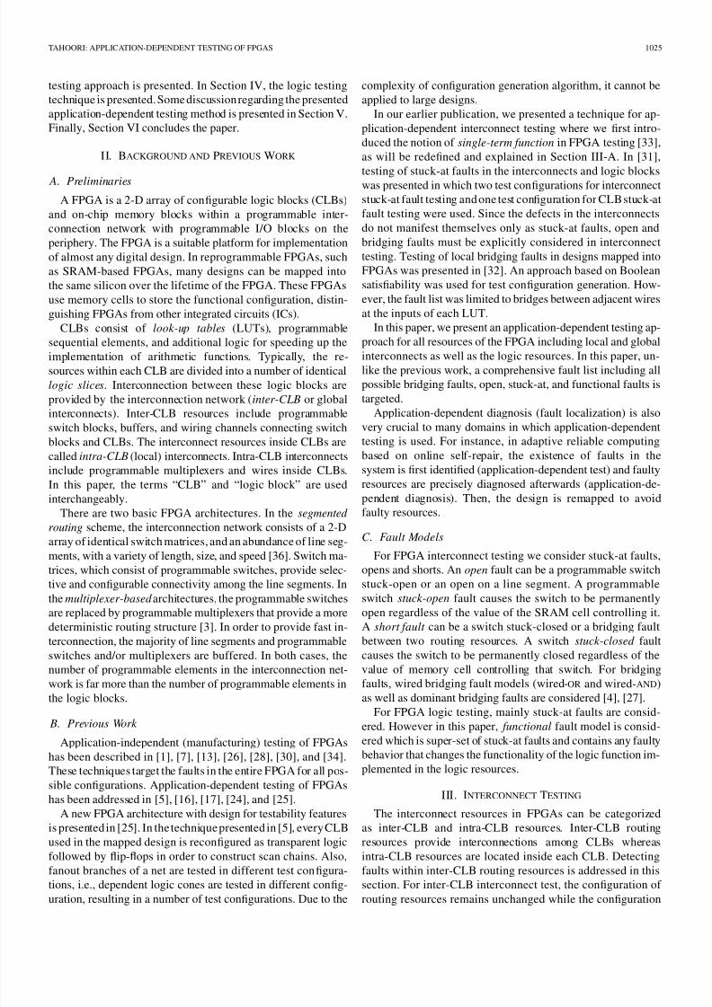
Fig. 1. Single-term function with activating input pattern.
of logic resources is modified. Testing of intra-CLB intercon-
nects along with logic resources are discussed in Section IV.
For this purpose, the configuration of used logic resources
(inclusive of intra-CLB interconnects) is kept unchanged while
the configuration of inter-CLB interconnects as well as unused
logic resources are changed.
The separation between inter-CLB and intra-CLB is made
because in contemporary FPGAs the programmable logic re-
sources are not limited to LUTs; other logic resources suchas carry generation/propagation logic and cascade chains are
included in CLBs. For inter-CLB interconnect testing, these
logic elements, if used in the original configuration, will be by-
passed. Therefore, no fault masking (causing undetected faults)
can occur due to existence of this circuitry in the interconnect
test mode.
More than 80% of the transistors in an FPGA are used in the
interconnect network. Also, more than eight metal layers are ex-
ploited for the wiring channels in the interconnection network
[6], [35]. Hence, the majority of the defects in an FPGA chip are
located in the interconnection network. These defects manifest
themselves as open and short (bridging) faults. Note that shortto the power rails in the interconnects are considered as conven-
tional stuck-at faults.
A. Testability of Single-Term Functions
A single-term function is a logic function which has only one
minterm or only one maxterm. In other words, the value of only
one term in the truth table is different from the value of all other
terms. The general form of a single-term function is a logic AND
or a logic OR function with possibly some inversions at the in-
puts and/or the output. The input combination corresponding to
this specific minterm (or maxterm) is called the activating input.
For a single-term function, if the applied input vector is the ac-
tivating input, all sensitized faults are detected. A fault is sensi-
tized if the values of the signals at the fault site are different from
faulty values. An example of a single-term function is shown in
Fig. 1, which is an OR function with inversions at the second
and fourth inputs. This function has only one maxterm. Since
the activating input (0101) is applied, ( stuck-at-1 fault),
, , , and are detected. Moreover, the bridging
faults between and , , , and
are also detected. If this function is implemented in a LUT, the
above mentioned faults in the inputs and output of that LUT will
be detected.
The following theorem generalizes the previous example and
expresses the conditions for detectability of faults in single-termfunctions.
Theorem 1: For a single-term function , if the applied
input vector is the activating input , all sensitized stuck-at and
bridging faults are detected.
Proof: Consider a fault (stuck-at or bridging fault) such
that it is sensitized. This means that if is a stuck-at fault ,
is set to by applying , and if is a bridging fault ,
, and are set to different values. In order to detect , it is onlysuf ficient to propagate the fault to the output. Since the fault
is already sensitized, the fault term, the term corresponding to
the faulty inputs , is different from the original term , i.e.,
. Because the original term is the activating term and
the value of the fault term is different from the value of the
original term , as is a single-term. Hence,
the fault-free output is different from the faulty output and the
fault is detected.
The interesting testing property of single-term functions
holds for any combinational network of single-term functions,
as expressed by the following theorem.
Theorem 2: Consider a network of single-term functions ,
and the input pattern , such that the values of the inputs of every function form the activating input of that function. Then,
all the sensitized faults are detected. In other words, for every
net with value , stuck-at is detected, and for each pair
of nets, and , with , the bridging fault between
and is detected.
Proof: In order to detect the fault, the fault effect must be
propagated from the fault site to the primary outputs. The proof
is based on an induction on the number of functions on the fault
propagation path from the fault site to the primary outputs. The
basis of the induction, only one function in the fault propagation
path, is expressed in Theorem 1, and therefore, is proven. Con-
sider a fault propagation path with 1 functions. Basedon Theorem 1, the fault effect at the input of the first function
on this path will be propagated to its output since the values ap-
pearing at the inputs of this function form its activating input.
The fault effect appearing at the output of the first function along
the path behaves as a stuck-at fault at the corresponding input
of the second function along the path (the one connected to the
output of the first function). Now, the situation is a fault prop-
agation path of 1 functions with a stuck-at fault at the fault
site. Based on the induction hypothesis, the fault effect will ap-
pear at the primary outputs.
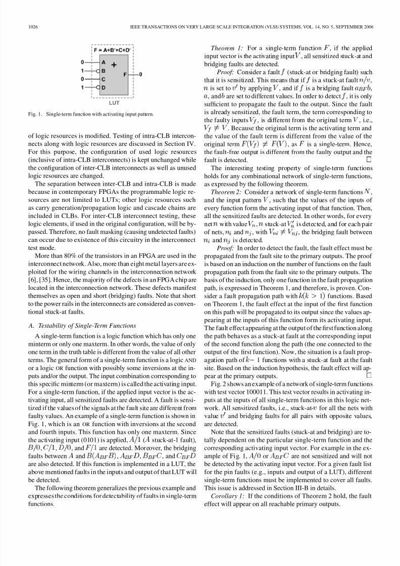
Fig. 2 shows an example of a network of single-term functions
with test vector 100011. This test vector results in activating in-
puts at the inputs of all single-term functions in this logic net-
work. All sensitized faults, i.e., stuck-at- for all the nets with
value and bridging faults for all pairs with opposite values,
are detected.
Note that the sensitized faults (stuck-at and bridging) are to-
tally dependent on the particular single-term function and the
corresponding activating input vector. For example in the ex-
ample of Fig. 1, or are not sensitized and will not
be detected by the activating input vector. For a given fault list
for the pin faults (e.g., inputs and output of a LUT), different
single-term functions must be implemented to cover all faults.
This issue is addressed in Section III-B in details.
Corollary 1: If the conditions of Theorem 2 hold, the faulteffect will appear on all reachable primary outputs.
8/7/2019 app depedent testing
http://slidepdf.com/reader/full/app-depedent-testing 4/10
TAHOORI: APPLICATION-DEPENDENT TESTING OF FPGAS 1027
Fig. 2. Logic network of single-term functions.
Proof: Consider the logic cone(s) originating from the fault
site(s) towards the primary outputs. Based on Theorem 1 and 2,
for any function in the fault cone that the fault effect appears
at its input, the fault effect will be propagated to its output as
well. Therefore, the fault effect will be propagated to all primary
outputs that are structurally reachable from the original fault
site.
Corollary 2: If the conditions of Theorem 2 hold, all possible
combinations of multiple faults which are sensitized will be de-
tected.
Proof: Based on Theorem 1 and 2, the fault effect ap-
pearing at the input of any function will be propagated to
its output. In other words, no fault masking occurs in such
logic network with the given conditions for the primary input
vector. Therefore, the fault effects corresponding to multiple
faults (e.g., multiple stuck-at faults, multiple bridging faults,combination of stuck-at and bridging faults) will be propagated
in the fault cones corresponding to each fault and appear at the
reachable primary outputs.
Similar testability properties exist in sequential networks of
single-term functions. However, the initial state of the circuit,
which is set by the primary input vector and the present value of
bistables (data flip-flop or latches) must satisfy the conditions of
Theorem 2. Moreover, the same input vector must be applied to
the circuit for a number of clock cycles to ensure that the fault
effect captured in any bistable will be propagated to the primary
outputs. The number of these test clock cycles depends on the
maximum sequential depth of the network, which is the numberof bistables along the longest path from any primary input to
any reachable primary output. The following lemma formally
expresses these conditions for a sequential network.
Lemma 1: Consider a sequential network consisting of only
single-term combinational functions and data flip-flops (D-FF)
or latches. If the primary input vector and the preset values of the
latches (or flip-flops) are set such that the value appearing at the
inputs of each single-term function form its activating input, all
the sensitized faults will be detected provided the same primary
input vector is kept unchanged for clock cycles, where is
equal to the sequential depth of this circuit.
Proof: Since the initial state of the bistables are set such
that to satisfy the conditions of the Theorem 2, the behavior of this circuit in the first clock cycle is exactly similar to a com-
Fig. 3. Sequential logic network of single-term functions.
Fig. 4. Sequential network of single-term functions with feedbacks.
binational circuit satisfying those conditions. Therefore, based
on Theorem 2, all sensitized faults will be propagated to the
primary outputs and/or captured in bistable(s) by the first appli-
cation of the clock pulse. Any fault captured in a bistable be-
haves as a stuck-at fault at the data output of that bistable in
the next clock cycle. This fault will be captured in the next rank
of bistables or will be propagated to the primary outputs in thenext clock cycle. Therefore, in order to propagate the fault ef-
fect captured in the first rank of the bistables in the first clock
cycle, at most clock cycles are required to propagate this fault
effect, level by level, to the primary outputs, where is equal to
the maximum number of bistables from any path from primary
inputs to the primary outputs (maximum sequential depth).
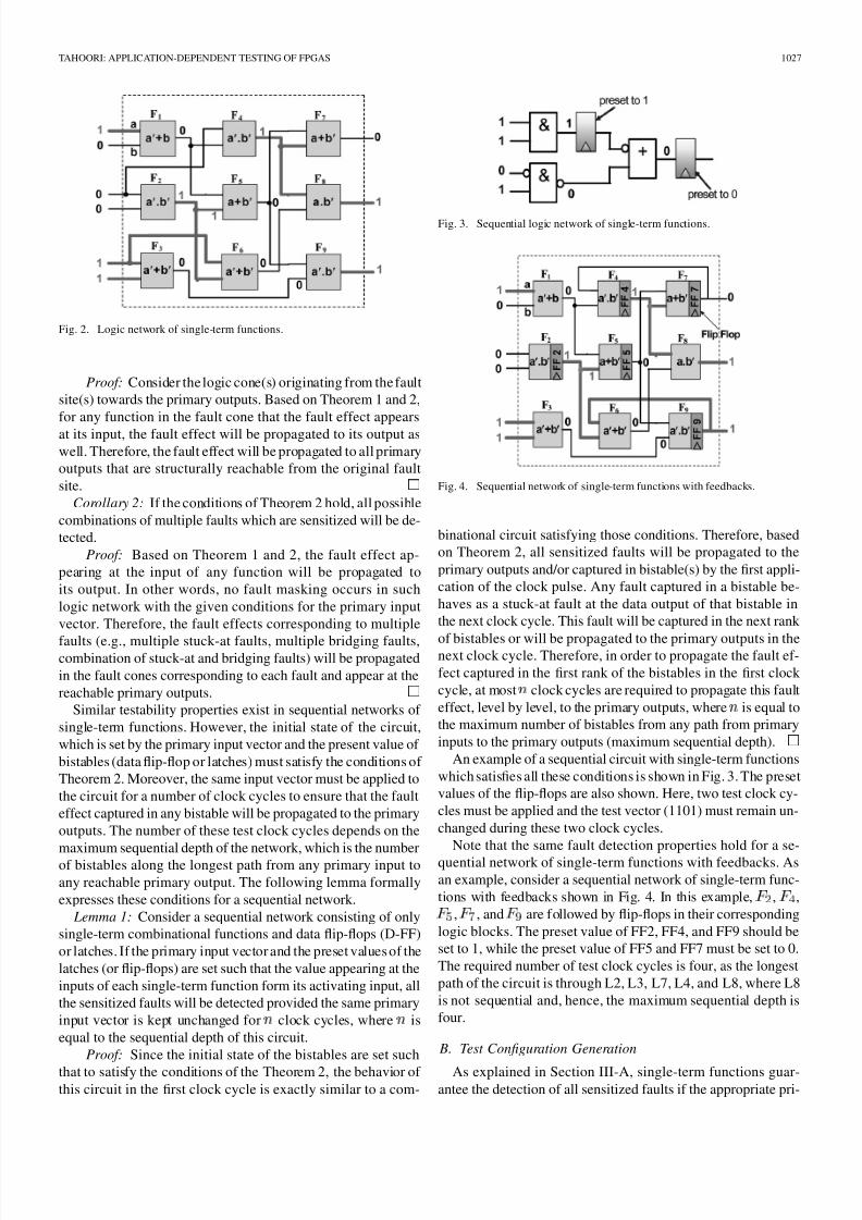
An example of a sequential circuit with single-term functions
which satisfies all these conditions is shown in Fig. 3. The preset
values of the flip-flops are also shown. Here, two test clock cy-
cles must be applied and the test vector (1101) must remain un-
changed during these two clock cycles.
Note that the same fault detection properties hold for a se-
quential network of single-term functions with feedbacks. As
an example, consider a sequential network of single-term func-
tions with feedbacks shown in Fig. 4. In this example, , ,
, , and are followed by flip-flops in their corresponding
logic blocks. The preset value of FF2, FF4, and FF9 should be
set to 1, while the preset value of FF5 and FF7 must be set to 0.
The required number of test clock cycles is four, as the longest
path of the circuit is through L2, L3, L7, L4, and L8, where L8
is not sequential and, hence, the maximum sequential depth is
four.
B. Test Configuration Generation
As explained in Section III-A, single-term functions guar-antee the detection of all sensitized faults if the appropriate pri-
8/7/2019 app depedent testing
http://slidepdf.com/reader/full/app-depedent-testing 5/10
1028 IEEE TRANSACTIONS ON VERY LARGE SCALE INTEGRATION (VLSI) SYSTEMS, VOL. 14, NO. 9, SEPTEMBER 2006
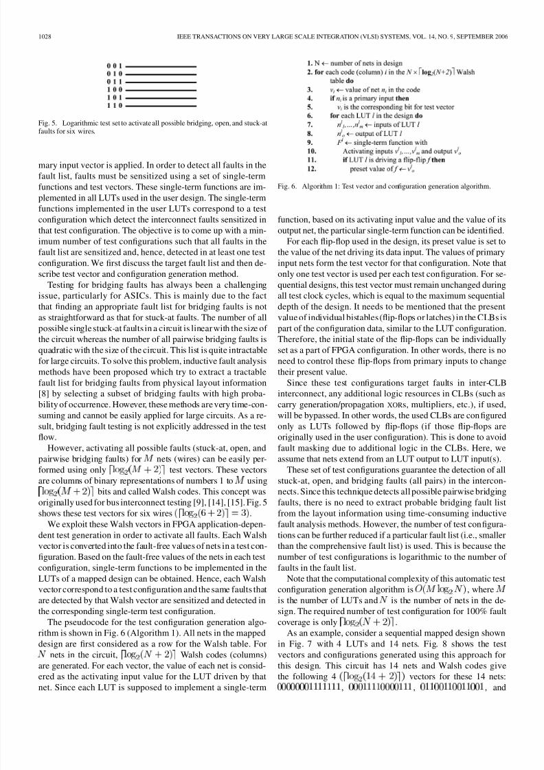
Fig. 5. Logarithmic test set to activate all possible bridging, open, and stuck-at
faults for six wires.
mary input vector is applied. In order to detect all faults in the
fault list, faults must be sensitized using a set of single-term
functions and test vectors. These single-term functions are im-
plemented in all LUTs used in the user design. The single-term
functions implemented in the user LUTs correspond to a test
configuration which detect the interconnect faults sensitized in
that test configuration. The objective is to come up with a min-
imum number of test configurations such that all faults in the
fault list are sensitized and, hence, detected in at least one test
configuration. We first discuss the target fault list and then de-
scribe test vector and configuration generation method.
Testing for bridging faults has always been a challenging
issue, particularly for ASICs. This is mainly due to the fact
that finding an appropriate fault list for bridging faults is not
as straightforward as that for stuck-at faults. The number of all
possible single stuck-at faults in a circuit is linear with the size of
the circuit whereas the number of all pairwise bridging faults is
quadratic with the size of the circuit. This list is quite intractable
for large circuits. To solve this problem, inductive fault analysis
methods have been proposed which try to extract a tractable
fault list for bridging faults from physical layout information
[8] by selecting a subset of bridging faults with high proba-
bility of occurrence. However, these methods are very time-con-suming and cannot be easily applied for large circuits. As a re-
sult, bridging fault testing is not explicitly addressed in the test
flow.
However, activating all possible faults (stuck-at, open, and
pairwise bridging faults) for nets (wires) can be easily per-
formed using only test vectors. These vectors
are columns of binary representations of numbers 1 to using
bits and called Walsh codes. This concept was
originally used for bus interconnect testing [9], [14], [15]. Fig. 5
shows these test vectors for six wires .
We exploit these Walsh vectors in FPGA application-depen-
dent test generation in order to activate all faults. Each Walshvector is converted into the fault-free values of nets in a test con-
figuration. Based on the fault-free values of the nets in each test
configuration, single-term functions to be implemented in the
LUTs of a mapped design can be obtained. Hence, each Walsh
vector correspond to a test configuration and the same faults that
are detected by that Walsh vector are sensitized and detected in
the corresponding single-term test configuration.
The pseudocode for the test configuration generation algo-
rithm is shown in Fig. 6 (Algorithm 1). All nets in the mapped
design are first considered as a row for the Walsh table. For
nets in the circuit, Walsh codes (columns)
are generated. For each vector, the value of each net is consid-
ered as the activating input value for the LUT driven by thatnet. Since each LUT is supposed to implement a single-term
Fig. 6. Algorithm 1: Test vector and configuration generation algorithm.
function, based on its activating input value and the value of its
output net, the particular single-term function can be identified.
For each flip-flop used in the design, its preset value is set to
the value of the net driving its data input. The values of primary
input nets form the test vector for that configuration. Note that
only one test vector is used per each test configuration. For se-
quential designs, this test vector must remain unchanged during
all test clock cycles, which is equal to the maximum sequential
depth of the design. It needs to be mentioned that the present
value of individual bistables (flip-flops or latches) in the CLBs is
part of the configuration data, similar to the LUT configuration.
Therefore, the initial state of the flip-flops can be individually
set as a part of FPGA configuration. In other words, there is no
need to control these flip-flops from primary inputs to change
their present value.
Since these test configurations target faults in inter-CLB
interconnect, any additional logic resources in CLBs (such as
carry generation/propagation XORs, multipliers, etc.), if used,will be bypassed. In other words, the used CLBs are configured
only as LUTs followed by flip-flops (if those flip-flops are
originally used in the user configuration). This is done to avoid
fault masking due to additional logic in the CLBs. Here, we
assume that nets extend from an LUT output to LUT input(s).
These set of test configurations guarantee the detection of all
stuck-at, open, and bridging faults (all pairs) in the intercon-
nects. Since this technique detects all possible pairwise bridging
faults, there is no need to extract probable bridging fault list
from the layout information using time-consuming inductive
fault analysis methods. However, the number of test configura-
tions can be further reduced if a particular fault list (i.e., smallerthan the comprehensive fault list) is used. This is because the
number of test configurations is logarithmic to the number of
faults in the fault list.
Note that the computational complexity of this automatic test
configuration generation algorithm is , where
is the number of LUTs and is the number of nets in the de-
sign. The required number of test configuration for 100% fault
coverage is only .
As an example, consider a sequential mapped design shown
in Fig. 7 with 4 LUTs and 14 nets. Fig. 8 shows the test
vectors and configurations generated using this approach for
this design. This circuit has 14 nets and Walsh codes give
the following 4 vectors for these 14 nets:, , , and

8/7/2019 app depedent testing
http://slidepdf.com/reader/full/app-depedent-testing 6/10
TAHOORI: APPLICATION-DEPENDENT TESTING OF FPGAS 1029
Fig. 7. Sequential design with 4 LUTs and 14 nets.
Fig. 8. Test vector and configurations for the circuit of Fig. 7.
. Each of these vectors is converted to a test
configuration by interpreting the value of each net in each test
vector as the activating value for that net.
The preset value of each value is also determined based on
the activating value of the net connected to its data input. The
configuration of each LUT is determined by the activating input
values for its input nets and the value of its output net. For ex-
ample, in the first configuration, the activating input values of
LUT L3 are and its output is . Since this is a single-term
function, it should be of AND type and . If the
output net is , such as L3 in the third configuration, the single
term function is OR type.
Proof of Fault Coverage
The proof of open, stuck-at, and bridging fault detection is
given below. Therefore, 100% fault coverage w.r.t. the fault list
given in Section II-C is achieved.
1) Detection of Open and Stuck-At Faults: For any inter-CLB
net inthe design, Algorithm 1 will assignit toboth 0 and 1 intwo
distinct test configurations. Since the single-term implementa-
tions of all LUTs are derived from the assigned values of the
nets, the conditions of Theorem 2 (as well as Lemma 1) will
be satisfied. Then, based on this theorem, both stuck-at-1 and
stuck-at-0 faults on all nets will be detected. Moreover, since
each net is assigned to opposite values and both stuck-at faultson the net are detected, the open fault will also be detected.
TABLE I
TEST CONFIGURATIONS FOR ISCAS’89 CIRCUITS
MAPPED INTO XILINX VIRTEX FPGAS
2) Detection of Bridging Fault: Consider a bridging fault be-
tween two arbitrary nets A and B. Algorithm 1 guarantees that
opposite values assigned into these nets (case 1: 0,
1, or case 2: 1, 0) in at least one test configuration.
Depending on the values of these two signals in that test con-
figuration and the particular bridging fault model (wired-AND,
wired-OR, or dominance), one of these nets gets a faulty value.For example, in case 1 if it is a wired-AND fault, then B becomes
faulty, or if it is a B-dominant fault, A becomes faulty. Since
conditions of Theorem 2 are guaranteed to be satisfied by Algo-
rithm 1, then the value of the faulty signal will be propagated to
reachable primary outputs and detected. Therefore, all pairwise
wired-OR, wired-AND, and dominant bridging faults will be de-
tected.
C. Results
Table I shows the number of test configurations required for
comprehensive application-dependent testing of the ISCAS’89
sequential circuits mapped into Xilinx Virtex FPGAs. Thesecond column shows the number of CLBs used for mapping
each circuit. The third column shows the number of faults
(pairwise bridging faults, opens, and single stuck-at faults)
in the fault list. The last column shows the number of test
configurations for 100% fault coverage (stuck-at, opens, and
bridging faults).
D. Upper-Bounds on Number of Test Con figurations
Here we estimate the maximum number of test configura-
tions for application-dependent interconnect testing for any
FPGA device. For this purpose, we calculate the upper bound
on the number of nets for an arbitrary design to be implemented
on an FPGA device with LUTs. Based on that, we figure outthe upper bound on the number of required test configurations

8/7/2019 app depedent testing
http://slidepdf.com/reader/full/app-depedent-testing 7/10
1030 IEEE TRANSACTIONS ON VERY LARGE SCALE INTEGRATION (VLSI) SYSTEMS, VOL. 14, NO. 9, SEPTEMBER 2006
TABLE II
MAXIMUM NUMBER OF TEST CONFIGURATIONS FOR XILINX VIRTEX II FPGAS
to detect all inter-CLB interconnect faults, as described inSection III-B.
Assume that the FPGA device has LUTs, and each LUT
has inputs. The upper bound onthe numberof netsfor any de-
signs to be mapped into this FPGA is , which is ba-
sically allocating one separate net for each input and the output
of every LUT in the FPGA. Note that this is a loose upper bound
since the LUT outputs are connected to the inputs of other LUTs,
and there are fanouts in the circuit. Using this upper bound on
the number of nets, the upper bound on the number of test con-
figurations based on the approach of Section III-B is as follows:
.
Table II shows these upper bounds on the number of inter-
connect test configurations for Xilinx Virtex II FPGA series
[36]. The number of LUTs for each device is shown in the
second column. Note that these LUTs have four inputs (
4). The upper bounds on the number of nets are shown in the
third column. The fourth column shows the number of all pair-
wise bridging faults associated with the maximum number of
nets. Note that the number of faults ranges from 3.3 10 to
1.08 10 depending on the size of the FPGA device. As can
be shown in this table, the number of test configuration for 100%
fault coverage ranges from 12 to 19. This confirms that this ap-
proach is absolutely tractable for the large FPGAs.
IV. LOGIC TESTING
This section describes the approach for testing faults located
inside the logic blocks, intra-CLB interconnects as well as
logic resources, used by the mapped design. In this approach,
the original configuration of the used logic blocks is preserved,
whereas the configuration of the global interconnects and
unused logic blocks are changed to exhaustively (and even
super-exhaustively) test all used logic blocks. This way, each
logic block is tested in the same conditions it is used in the
application configuration. On the other hand, changing the
configuration of the inter-CLB interconnects and unused logic
blocks allows us to facilitate the access to each logic block. This
approach can be framed as a BIST mechanism as describednext.
Fig. 9. (a) Original configuration. (b) BIST configuration to test used logic
blocks.
A. BIST Scheme
The key point of this approach is to keep the configuration of
used logic blocks unchanged while applying test and observing
the outputs of these logic blocks by exploiting inter-CLB in-
terconnects and unused logic blocks. In this scheme, each used
logic block will be exhaustively (or super-exhaustively) tested
while all these logic blocks are tested concurrently. Since the
number of the inputs of each logic block is very small (less than
ten inputs for each logic slice), it is practical to apply an exhaus-
tive test (all possible input combinations) or a super-exhaustive
test (all possible input transitions) for testing each used logic
block.
The global interconnect is reprogrammed in such a way that
the test signals are routed to each logic block. In other words, a
common bus which is routed using available unused routing re-sources in the test configuration directly connects the test signals
to each logic block. The size of the bus is equal to the number
of logic block inputs to apply an exhaustive test for each logic
block. This parallel connection allows testing the entire set of
logic blocks concurrently. The test signals can be connected to
the primary inputs for an off-chip test or to a test pattern gen-
erator implemented using unused on-chip resources for a BIST
implementation.
The logic block outputs are observed through an internal re-
sponse compactor. This way, the outputs of many logic blocks
can be observed using a small number of off-chip outputs. The
response compactor can be combined with a response predictorsuch that a unique pass/fail signal can be generated. Since the
user configuration of the logic blocks are known at the test time,
the response predictor can be precomputed and stored in the un-
used logic blocks (LUT bit locations or on-chip memory).
A BIST version of this test scheme is shown in Fig. 9. There
are three main components in this BIST scheme, namely test
pattern generator, parity predictor, and parity checker modules.
1) Test Pattern Generator (TPG): A linear feedback shift
register (LFSR) modified as a De Bruijn counter [21], imple-
mented in the unused logic blocks, generates the exhaustive se-
quence. It is also possible to generate a super-exhaustive test to
be able to also detect delay faults in the logic blocks by using
two LFSRs generating all possible transitions. Due to the smallnumber of logic block inputs which usually ranges from 3 to 5
8/7/2019 app depedent testing
http://slidepdf.com/reader/full/app-depedent-testing 8/10
TAHOORI: APPLICATION-DEPENDENT TESTING OF FPGAS 1031
per LUT (10–12 for a logic slice), an exhaustive or super-ex-
haustive testing of the logic block is performed with only a
small number of vectors. Moreover, since these test patterns are
generated on-chip, the test application time is also very small
compared to off-chip test application alternatives. All functional
faults inclusive of stuck-at faults are covered by this test.
2) Parity Predictor: An additional logic block generates aparity bit of the outputs of the logic blocks used in the user ap-
plication for each input combination of logic blocks. Hence, the
number of inputs of this parity predictor block is equal to the
number of inputs of the logic blocks since all logic blocks ob-
tain the same set of inputs from the test pattern generator in the
test mode. This parity predictor block stores the precomputed
parity of all user logic blocks for each input combination. There-
fore, unlike general combinational circuits where parity predic-
tion can be expensive [23], only one extra logic block is required
to implement the parity prediction circuitry. For each input com-
bination of the logic blocks, the parity bit according to the ex-
pected outputs of all logic blocks is precomputed (obtained by
simulation) and stored in the corresponding bit location of theLUT(s) implementing the parity predictor. As a result, the con-
figuration of the parity predictor block stores the precomputed
parity bits.
3) Parity Checker: The outputs of logic blocks and the parity
block are checked using a parity checker. The number of inputs
of this parity checker is equal to the number of used logic blocks
plus one, the output of the parity predictor. The simplest imple-
mentation of this parity checking module is a classical XOR tree.
If there are user logic blocks in the design and their outputs
are denoted by , then the parity checker implements
the function , using available unused logic
blocks. If any odd number of logic blocks produce erroneousoutputs, the errors will be detected by the parity checker. More
parity bits (similar to Hamming codes and extensions) can be in-
cluded to detect situations when even a number of logic blocks
produce errors. The parity checker is the largest module in the
BIST circuitry. Unlike the other two modules, TPG and parity
predictor, in which their sizes are independent of the size of the
mapped design, the size of the parity checker is a function of the
size of the mapped design (the number of user logic blocks).
The logic blocks in contemporary FPGAs contain other logic
components besides LUTs, such as carry generation and prop-
agation logic, cascade chains, and programmable multiplexers
[3], [36]. In the presented technique, all the resources in the user
logic blocks, inclusive of all logic resources and local intercon-
nect, will be tested exhaustively. Since the configuration of used
logic blocks are preserved, and the width of TPG is chosen to
generate tests for all used inputs of logic blocks, all used logic
resources and intra-CLB interconnect are tested.
One problem with this approach could be the routing con-
gestion since the test signals (LFSR outputs) must be routed to
the inputs of all used logic blocks. This could be a potential
problem for very large designs. In order to solve this problem,
the presented BIST architecture can be partitioned: instead of
connecting the outputs of one TPG to all logic blocks, multiple
TPGs can be used and the outputs of each TPG are connected
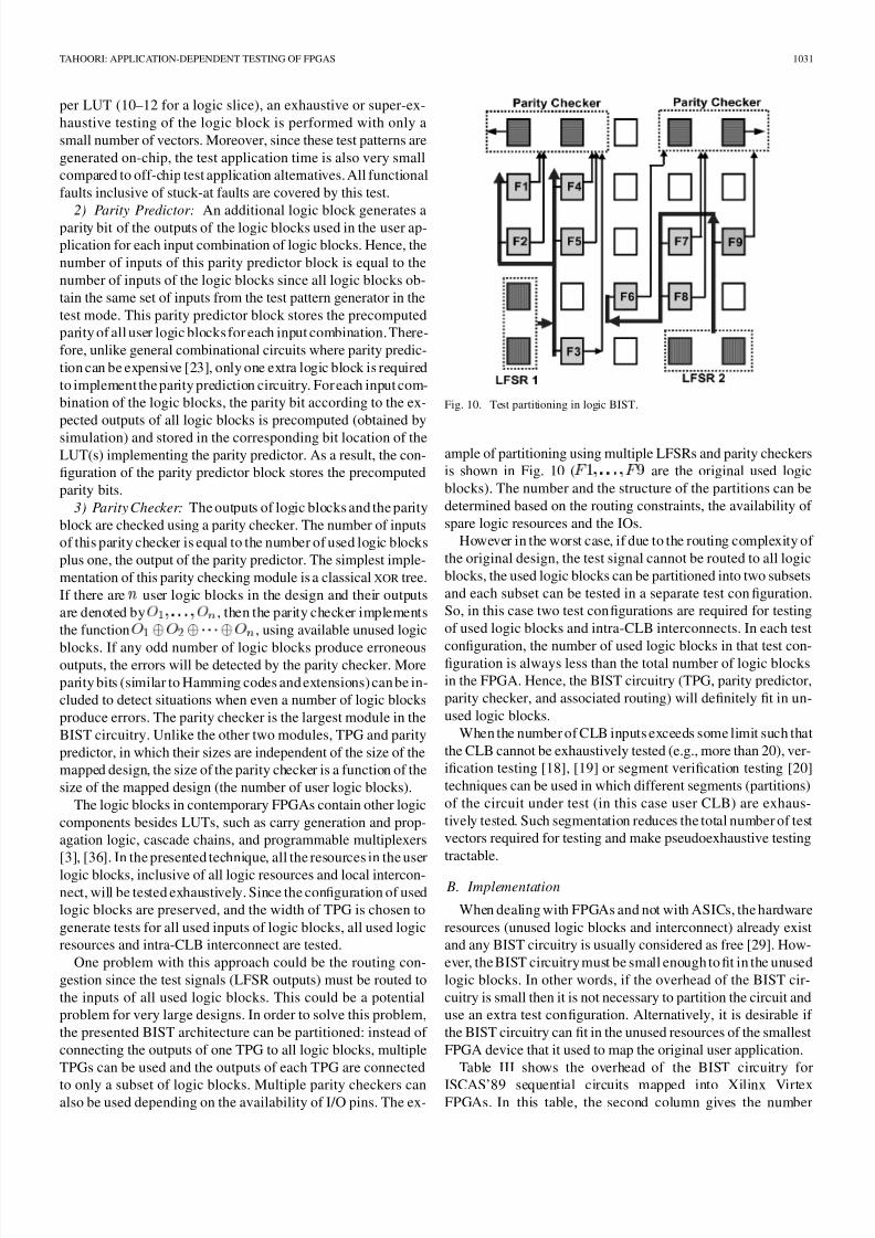
to only a subset of logic blocks. Multiple parity checkers canalso be used depending on the availability of I/O pins. The ex-
Fig. 10. Test partitioning in logic BIST.
ample of partitioning using multiple LFSRs and parity checkers
is shown in Fig. 10 ( are the original used logic
blocks). The number and the structure of the partitions can be
determined based on the routing constraints, the availability of
spare logic resources and the IOs.
However in the worst case, if due to the routing complexity of
the original design, the test signal cannot be routed to all logic
blocks, the used logic blocks can be partitioned into two subsets
and each subset can be tested in a separate test configuration.
So, in this case two test configurations are required for testing
of used logic blocks and intra-CLB interconnects. In each test
configuration, the number of used logic blocks in that test con-figuration is always less than the total number of logic blocks
in the FPGA. Hence, the BIST circuitry (TPG, parity predictor,
parity checker, and associated routing) will definitely fit in un-
used logic blocks.
When the number of CLB inputs exceeds some limit such that
the CLB cannot be exhaustively tested (e.g., more than 20), ver-
ification testing [18], [19] or segment verification testing [20]
techniques can be used in which different segments (partitions)
of the circuit under test (in this case user CLB) are exhaus-
tively tested. Such segmentation reduces the total number of test
vectors required for testing and make pseudoexhaustive testing
tractable.
B. Implementation
When dealing with FPGAs and not with ASICs, the hardware
resources (unused logic blocks and interconnect) already exist
and any BIST circuitry is usually considered as free [29]. How-
ever, the BIST circuitry must be small enough to fit in the unused
logic blocks. In other words, if the overhead of the BIST cir-
cuitry is small then it is not necessary to partition the circuit and
use an extra test configuration. Alternatively, it is desirable if
the BIST circuitry can fit in the unused resources of the smallest
FPGA device that it used to map the original user application.
Table III shows the overhead of the BIST circuitry for
ISCAS’89 sequential circuits mapped into Xilinx VirtexFPGAs. In this table, the second column gives the number

8/7/2019 app depedent testing
http://slidepdf.com/reader/full/app-depedent-testing 9/10
1032 IEEE TRANSACTIONS ON VERY LARGE SCALE INTEGRATION (VLSI) SYSTEMS, VOL. 14, NO. 9, SEPTEMBER 2006
TABLE III
OVERHEAD OF BIST LOGIC TESTING
of CLBs required to implement the original circuit, the third
column represents the number of CLBs required to implement
the entire BIST scheme with the LFSR, parity predictor, andparity checker as well as the circuit under test (original user
configuration). Note that each CLB in Xilinx Virtex FPGAs
contains four LUTs and storage elements. The overhead is
given in the fourth column as a percentage of the initial circuit
implementation. The overhead for bigger circuits is much
smaller. For the circuits with zero overhead, it was possible to
map the entire BIST circuitry in the unused LUTs and logic
slices of the partially-used CLBs by the original design. Since
the increase in the CLB usage is only a few percents, the entire
BIST circuitry will still fit into the smallest FPGA device that
the original design would fit.
V. DISCUSSION
In the presented interconnect testing method, the original con-
figuration of the routing resources of the design remains un-
changed. Also, the timing of the original design is preserved,
i.e., no flip-flop is added to or removed from the original design
in test configurations; only the preset values of some flip-flops
are modified. The advantages of this approach are as follows.
1) Reduced Test Con figuration Generation Effort: There is
no need to perform placement and routing for generating the test
configurations. The placement and routing of the original design
are used for the test configurations.
2) No Fault Missed: Since no partitioning of the resourcesover multiple configurations is performed, no fault is missed
by decomposition. For example, bridging faults between the re-
sources decomposed into different test configurations cannot be
detected [5]. This situation never happens in our approach.
3) Test Time Reduction: The only difference among the test
configurations is the contents of the LUTs, which is a very small
portion of the configuration data (less than 5% of the total con-
figuration bits [36]). Therefore, test configuration loading timecan be drastically reduced by partial reconfiguration. For ex-
ample, the reconfiguration scheme in Xilinx FPGAs is frame-
based. Each CLB column is divided into a number of frames.
Some frames contain configuration bits for both logic and in-
terconnects whereas others contain only interconnect configu-
ration bits. The partial reconfiguration for loading next test con-
figuration requires loading only those frames containing logic
configuration bits.
4) Test Con figuration Compression: As the only difference
among the original design and the test configurations is the con-
tents of LUTs, instead of saving the complete configuration
data for each test configurations, only the LUT contents need to
be stored for each test configuration (differential compression),achieving up to 20 test configuration compression ratio.
5) Compatibility: This technique relies only on repro-
grammability of logic resources. This feature exists in all
families of reprogrammable (SRAM-based) FPGAs and
complex programmable logic devices (CPLDs). Hence, this
technique can be easily applied for various FPGA or CPLD
families from a variety of programmable logic vendors [3],
[36].
The presented techniques for testing interconnect and logic
resources are also able to detect the faults that occur in the con-
figuration circuitry. The faults in the routing configuration bits
manifest themselves as open and bridging faults in the mappeddesign which will be detected in the first set of test configura-
tions (Section III). Faults in the logic configuration bits affect
the functionality of the logic blocks which will be detected in
the logic BIST method (Section IV).
Note that a bridging fault between a signal line and a configu-
ration line will directly or indirectly affect the user application.
If the value of the signal line is disturbed, the user application
is directly affected and depending whether this signal line is a
global interconnect or inside a CLB, it will be detected in the
first or second set of test configurations. If the bridging fault only
disturbs the configuration line and it then affects the state of a
configuration bit, it results in a fault in the interconnect (open
or bridging fault) or logic resources (logic fault). The presented
test methods are able to detect this fault.
Since the logic is modified for interconnect testing and the in-
terconnect is modeled for logic testing, there might be a situation
in which there is a fault in the resources used to test but not used
for the application. By performing high-resolution diagnosis, it
can be identified whether the defective resources are used in the
user application or not. Once the failure is diagnosed to be in
a resource not originally utilized by the user application, then
it becomes a reliability and test quality issue. If the defective
resource is physically very close to user resources, then based
on reliability constraints and criticality of the application, the
design might be remapped such that the used resources by theapplication is not too close to the defective resources since the

8/7/2019 app depedent testing
http://slidepdf.com/reader/full/app-depedent-testing 10/10
TAHOORI: APPLICATION-DEPENDENT TESTING OF FPGAS 1033
defect might expand over time and make the neighboring re-
sources defective, as well.
VI. CONCLUSION
In this paper, a new technique for application-dependent
testing of FPGAs is presented. This method tests all inter-
connect as well as logic resources used by a particular userapplication implemented on an FPGA. In the first phase, only
the configuration of logic blocks is modified for global inter-
connect testing. Less than 20 test configurations are required
to test the largest design implemented in the largest FPGA
device for all stuck-at, open, and pairwise bridging faults. The
second phase, which consists of only one test configuration,
tests all used logic blocks as well as local interconnects. In
this phase, the configuration of original used logic blocks is
preserved and configuration of interconnects and unused logic
blocks is changed to exhaustively test all used logic blocks.
A BIST version of the presented test configurations is also
presented. The experimental results show that the overhead of
BIST circuitry, in terms of the number of required unused logic
blocks, is reasonably small.
The presented techniques can be used either as part of a
ASFPGA test flow, or as an online testing method in a self-re-
pair scheme for defect and fault tolerance.
REFERENCES
[1] M. Abramovici and C. Stroud, “BIST-based detection and diagnosisof multiple faults in FPGAs,” in Proc. IEEE Int. Test Conf., 2000, pp.785–794.
[2] M. J. Alexander and G. Robins, “New performance-driven FPGArouting algorithms,” IEEE Trans. Comput.-Aided Des. Integr. Circuits
Syst., vol. 15, no. 12, pp. 1505–1517, Dec. 1996.
[3] “ Altera Data Sheets,” 2004, [Online]. Available: http://www.al-tera.com[4] B. Chess and T. Larrabee, “Logic testing of bridging faults in CMOS
integrated circuits,” IEEE Trans. Comput., vol. 47, no. 3, pp. 338–345,Mar. 1998.
[5] D. Das and N. A. Touba, “A low cost approach for detecting, locating,and avoiding interconnect faults in FPGA-based reconfigurable sys-tems,” in Proc. Int. Conf. VLSI Des., 1999, pp. 266–269.
[6] A. DeHon, “Balancing interconnect and computation in a reconfig-urable computing array (or, why you don’t really want 100% LUT uti-lization),” in Proc. ACM Int. Symp. FPGAs, 1999, pp. 69–78.
[7] A. Doumar and H. Ito, “Testing the logic cells and interconnect re-sources for FPGAs,” in Proc. Asian Test Conf., 1999, pp. 369–374.
[8] F. J. Ferguson and J. P. Shen, “A CMOS fault extractor for inductive
fault analysis,” IEEE Trans. Comput.-Aided Des. Integr. Circuits Syst.,vol. 7, no. 11, pp. 1181–1194, Nov. 1988.
[9] P. Goel and M. T. McMahon, “Electronic chip-in place test,” in Proc.
IEEE Int. Test Conf., 1982, pp. 83–90.[10] I. G. Harris, P. R. Menon, and R. Tessier, “BIST-based delay path
testing in FPGA architectures,” in Proc. IEEE Int. Test Conf., 2001,pp. 932–938.
[11] G. Harris and R. Tessier, “Interconnect testing in cluster-based FGPAarchitectures,” in Proc. Des. Autom. Conf., 2000, pp. 49–54.
[12] W. J. Huang and E. J. McCluskey, “Column-based precompiled con-
figuration techniques for FPGA fault tolerance,” in Proc. IEEE Symp.Field-Programmable Custom Comput. Mach., 2001, pp. 137–146.
[13] W. K. Huang, X. T. Chen, and F. Lombardi, “On the diagnosis of programmable interconnect systems: Theory and application,” in Proc.
VLSI Test Symp., 1996, pp. 204–209.[14] H. Jarwala and C. W. Yau, “A new framework for analyzing test gen-
eration and diagnosis algorithms for wiring networks,” in Proc. IEEE
Int. Test Conf., 1989, pp. 63–70.[15] W. H. Kautz, “Testing for faults in wiring networks,” IEEE Trans.
Comput., vol. C-23, no. 4, pp. 358–363, Apr. 1974.[16] A. Krasniewski, “Application-dependent testing of FPGA delayfaults,”
in Proc. Euromicro. Conf., 1999, pp. 260–267.
[17] ——, “Exploiting reconfigurability for effective testing of delay faultsin sequential subcircuits of LUT-based FPGAs,” in Proc. Field Pro-
grammable Logic Conf., 2002, pp. 616–626.[18] E. J. McCluskey and S. Bozorgui-Nesbat, “Design for autonomous
test,” IEEE Trans. Circuit Syst., vol. 28, no. 11, pp. 1070–1079, Nov.1981.
[19] E. J. McCluskey, “Built-in verification test,” in Proc. IEEE Int. Test
Conf., 1982, pp. 183–190.
[20] ——, “Verification testing—A pseudoexhaustivetest technique,” IEEE Trans. Comput., vol. C-33, no. 6, pp. 541–546, Jun. 1984.[21] —— , Logic Design Principles. Englewood Cliffs, NJ: Prentice-Hall,
1986.[22] H. Michinishi, T. Yokohira, and T. Okamoto, “A test methodology
for interconnect structures of LUT-based FPGAs,” in Proc. Asian Test
Symp., 1996, pp. 68–74.[23] S. Mitra and E. J. McCluskey, “Which concurrent error detection
scheme to choose,” in Proc. IEEE Int. Test Conf., 2000, pp. 985–994.[24] W.Quddus, A.Jas,and N.A. Touba, “Configuration self-test in FPGA-
based reconfigurable systems,” in Proc. Int. Symp. Circuits Syst., 1999,pp. 97–100.
[25] M. Renovell, P. Faure, J. M. Portal, J. Figueras, and Y. Zorian, “Is-FPGA: A new symmetric FPGA architecture with implicit scan,” inProc. IEEE Int. Test Conf., 2001, pp. 924–931.
[26] M. Renovell and Y. Zorian, “Different experiments in test generationfor XILINX FPGAs,” in Proc.IEEE Int. TestConf., 2000,pp. 854–862.
[27] T. Storey and W. Maly, “CMOS bridging fault detection,” in Proc. IEEE Int. Test Conf., 1990, pp. 842–851.
[28] C. Stroud, S. Wijesuriya, C. Hamilton, and M. Abramovici, “Built-inself-test of FPGA interconnect,” in Proc. IEEE Int. Test Conf., 1998,pp. 404–411.
[29] C. Stroud,S. Konala, C. Ping, and M. Abramovici, “Built-in self-test of logic blocksin FPGAs(Finally, a free lunch: BIST withoutoverhead!),”in Proc. VLSI Test Symp., 1996, pp. 387–392.
[30] X.Sun,J. Xu, B. Chan,and P.Trouborst, “Novel technique for built-in-self test of FPGA interconnects,” in Proc. IEEE Int. Test Conf., 2000,pp. 795–803.
[31] M. B. Tahoori, E. J. McCluskey, M. Renovell, and P. Faure, “A multi-configuration strategy for an application dependent testing of FPGAs,”in Proc. VLSI Test Symp., 2004, pp. 154–159.
[32] M. B. Tahoori, “Application-specific bridging fault testing of FPGAs,” J. Electron. Testing, Theory, Appl., vol. 20, no. 3, pp. 279–289, Jun.
2004.[33] ——, “Application-dependent testing of FPGA interconnects,” in Proc.
Int. Symp. Defect Fault Tolerance, 2003, pp. 409–416.[34] M. B. Tahoori and S. Mitra, “Automatic configuration generation
for FPGA interconnect testing,” in Proc. VLSI Test Symp., 2003, pp.134–139.
[35] A. Takahara, T. Miyazaki, T. Murooka, M. Katayama, K. Hayashi, A.Tsutsui, T. Ichimori, and K. Fukami, “More wires and fewer LUTs:A design methodology for FPGAs,” in Proc. ACM Int. Symp. FPGAs,
1998, pp. 12–19.[36] “The Programmable Logic Data Book,” Xilinx Inc, 2003.
[37] Xilinx Easypath Solutions 2003 [Online]. Available: http://www.xilinx.com
Mehdi B. Tahoori (S’02–M’04) received the M.S.degree in electrical engineering from StanfordUniversity, Palo, Alto, CA, in 2002, the B.S. degree
in computer engineering from Sharif University of Technology, Tehran, Iran, in 2000, and the Ph.D.degree in electrical engineering from StanfordUniversity, in 2003, under the supervision of Prof.E. J. McCluskey,
He is an Assistant Professor in the Department of Electrical and Computer Engineering at NortheasternUniversity, Boston, MA. During 2002–2003, he was
a Research Scientist at Fujitsu Laboratories of America in advanced computer-aided design (CAD) research working on reliability issues in deep-submicronmixed-signal VLSI designs. He has published more than 60 technical papers
in leading conferences and journals. His research interests include nanotech-nology, VLSI testing, VLSI CAD, and fault tolerant computing.
Dr.Tahoori hasbeen theProgram Chair of theIEEE Defectand CurrentBasedTesting Workshop in 2005 and 2006. He was the Guest Editor of IEEE Designand Test Special Issue on Advanced Technologies and Reliable Design for Nan-otechnology Systems. He has served on the program committees of IEEE Inter-national Test Synthesis Workshop and IEEE International Workshop on Designand Test of Defect-Tolerant Nanoscale Architectures.