ap60n03d 60a 30v to-252
TRANSCRIPT
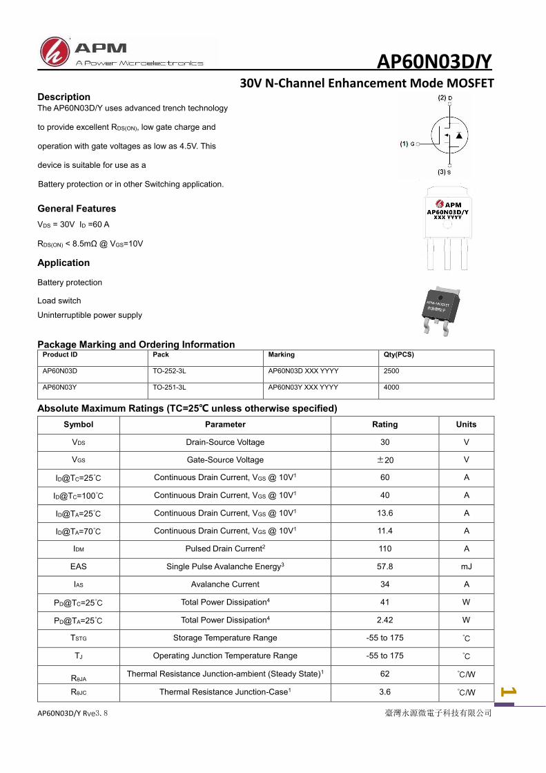
AP60N03DIY
30V N-Channel Enhancement Mode MOSFET
AP60N03D/Y Rve3.8 臺灣永源微電子科技有限公司
1
Description The AP60N03D/Y uses advanced trench technology
to provide excellent RDS(ON), low gate charge and
operation with gate voltages as low as 4.5V. This
device is suitable for use as a
Battery protection or in other Switching application.
General Features
VDS = 30V ID =60 A
RDS(ON) < 8.5mΩ @ VGS=10V
Application
Battery protection
Load switch
Uninterruptible power supply
Package Marking and Ordering Information
Product ID Pack Marking Qty(PCS)
AP60N03D AP60N03D XXX YYYY 2500
AP60N03Y AP60N03Y XXX YYYY 4000
Absolute Maximum Ratings (TC=25℃ unless otherwise specified)
Symbol Parameter Rating Units
VDS Drain-Source Voltage 30 V
VGS Gate-Source Voltage ±20 V
ID@TC=25℃ Continuous Drain Current, VGS @ 10V1 60 A
ID@TC=100℃ Continuous Drain Current, VGS @ 10V1 40 A
ID@TA=25℃ Continuous Drain Current, VGS @ 10V1 13.6 A
ID@TA=70℃ Continuous Drain Current, VGS @ 10V1 11.4 A
IDM Pulsed Drain Current2 110 A
EAS Single Pulse Avalanche Energy3 57.8 mJ
IAS Avalanche Current 34 A
PD@TC=25℃ Total Power Dissipation4 41 W
PD@TA=25℃ Total Power Dissipation4 2.42 W
TSTG Storage Temperature Range -55 to 175 ℃
TJ Operating Junction Temperature Range -55 to 175 ℃
RθJA Thermal Resistance Junction-ambient (Steady State)1 62 ℃/W
RθJC Thermal Resistance Junction-Case1 3.6 ℃/W
TO-252-3L
TO-251-3L
AP60N03DIY
30V N-Channel Enhancement Mode MOSFET
AP60N03D/Y Rve3.8 臺灣永源微電子科技有限公司
2
Electrical Characteristics (TJ=25 ℃, unless otherwise noted)
Symbol Parameter Conditions Min. Typ. Max. Unit
BVDSS Drain-Source Breakdown Voltage VGS=0V , ID=250uA 30 --- --- V
△BVDSS/△TJ BVDSS Temperature Coefficient Reference to 25℃ , ID=1mA --- 0.027 --- V/℃
RDS(ON) Static Drain-Source On-Resistance2
VGS=10V , ID=30A --- 7.5 8.5
mΩ VGS=4.5V , ID=15A --- 11 14 VGS(th) Gate Threshold Voltage
VGS=VDS , ID =250uA 1.2 1.5 2.5 V
△VGS(th) VGS(th) Temperature Coefficient --- -5.8 --- mV/℃
IDSS Drain-Source Leakage Current VDS=24V , VGS=0V , TJ=25℃ --- --- 1
uA VDS=24V , VGS=0V , TJ=55℃ --- --- 5
IGSS Gate-Source Leakage Current VGS=±20V , VDS=0V --- --- ±100 nA
gfs Forward Transconductance VDS=5V , ID=30A --- 38 --- S
Rg Gate Resistance VDS=0V , VGS=0V , f=1MHz --- 2.2 3.5
Qg Total Gate Charge (4.5V)
VDS=15V , VGS=4.5V , ID=15A
--- 12.6 17.6
nC Qgs Gate-Source Charge --- 4.2 5.9
Qgd Gate-Drain Charge --- 5.1 7.1
Td(on) Turn-On Delay Time
VDD=15V , VGS=10V , RG=3.3
ID=15A
--- 4.6 9.2
ns Tr Rise Time --- 12.2 22
Td(off) Turn-Off Delay Time --- 26.6 53
Tf Fall Time --- 8 16
Ciss Input Capacitance
VDS=15V , VGS=0V , f=1MHz
--- 1317 1843
pF Coss Output Capacitance --- 163 228
Crss Reverse Transfer Capacitance --- 131 183
IS Continuous Source Current1,5 VG=VD=0V , Force Current
--- --- 55 A
ISM Pulsed Source Current2,5 --- --- 110 A
VSD Diode Forward Voltage2 VGS=0V , IS=1A , TJ=25℃ --- --- 1.2 V
trr Reverse Recovery Time IF=30A , dI/dt=100A/µs ,
TJ=25℃
--- 9.2 --- nS
Qrr Reverse Recovery Charge --- 2 --- nC
Note : 1 .The data tested by surface mounted on a 1 inch2 FR-4 board with 2OZ copper.
2.The data tested by pulsed , pulse width ≦ 300us , duty cycle ≦ 2%
3.The EAS data shows Max. rating . The test condition is VDD=25V,VGS=10V,L=0.1mH,IAS=34A
4.The power dissipation is limited by 175℃ junction temperature 5.The data is theoretically the same as ID and IDM , in real applications , should be limited by total power
dissipation.
AP60N03DIY
30V N-Channel Enhancement Mode MOSFET
AP60N03D/Y Rve3.8 臺灣永源微電子科技有限公司
3
0
25
50
75
100
0 0.5 1 1.5 2 2.5 3VDS , Drain-to-Source Voltage (V)
ID D
rain
Cu
rre
nt (A
)
VGS=10V
VGS=7V
VGS=5V
VGS=4.5V
VGS=3V
0
3
6
9
12
0 0.3 0.6 0.9 1.2
VSD , Source-to-Drain Voltage (V)
IS(A
)
TJ=25℃TJ=150℃
0
2
4
6
8
10
0 6 12 18 24 30QG , Total Gate Charge (nC)
VG
S , G
ate
to
So
urc
e V
olta
ge
(V
)
ID=15A
VDS=24V
VDS=15V
0.2
0.6
1
1.4
1.8
-50 25 100 175
TJ ,Junction Temperature (℃ )
Norm
aliz
ed V
GS
(th)
0.2
0.6
1.0
1.4
1.8
-50 -5 40 85 130 175
TJ , Junction Temperature (℃)
Norm
aliz
ed O
n R
esis
tance
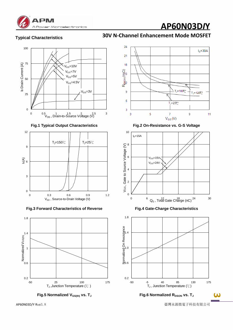
Fig.1 Typical Output Characteristics Fig.2 On-Resistance vs. G-S Voltage
Fig.3 Forward Characteristics of Reverse
diode
Fig.4 Gate-Charge Characteristics
Fig.5 Normalized VGS(th) vs. TJ Fig.6 Normalized RDSON vs. TJ
Typical Characteristics

AP60N03DIY
30V N-Channel Enhancement Mode MOSFET
AP60N03D/Y Rve3.8 臺灣永源微電子科技有限公司
4
10
100
1000
10000
1 5 9 13 17 21 25
VDS , Drain to Source Voltage (V)
Ca
pa
cita
nce
(p
F)
F=1.0MHz
Ciss
Coss
Crss
0.01
0.1
1
0.00001 0.0001 0.001 0.01 0.1 1
t , Pulse Width (s)
Norm
aliz
ed T
herm
al R
esponse (
RθJC)
PDM
D = TON/T
TJpeak = TC + PDM x RθJC
TON
T
0.02
0.01
0.05
0.1
0.3
DUTY=0.5
SINGLE PULSE
Td(on) Tr
Ton
Td(off) Tf
Toff
VDS
VGS
90%
10%
IAS
VGS
BVDSS
VDD
EAS=1
2L x IAS
2 x
BVDSS
BVDSS-VDD
Fig.8 Safe Operating Area
Fig.9 Normalized Maximum Transient Thermal Impedance
Fig.7 Capacitance
Fig.10 Switching Time Waveform Fig.11 Unclamped Inductive Switching Waveform

AP60N03DIY
30V N-Channel Enhancement Mode MOSFET
AP60N03D/Y Rve3.8 臺灣永源微電子科技有限公司
5
Package Mechanical Data
Dimensions
Millimeters InchesRef.
Min. Typ. Max. Min. Typ. Max.
A
A2
B
C
D
E
G
H
L
V1
V2
2.10
0
0.66
0.40
2.50
0.10
0.86
0.60
0.083
0
0.026
0.016
0.098
0.004
0.034
0.024
6.40
9.50 10.70 0.374 0.421
0.053 0.065
5.90 6.30
L2
0° 6°
0.232 0.248
6.80 0.252 0.268
4.47 4.67 0.176 0.184
1.09 1.21 0.043 0.048
7°
1.35 1.65
0° 6°
7°
B2 5.18 5.48 0.202 0.216
C2 0.44 0.58 0.017 0.023
D1
E1
5.30REF
4.63 0.182
0.209REF
B2
E
H
B
G
LC2
DETAIL A
DETAIL A
A
C
V1
V1
V2
A2
D
V1
E1
D1
L2
TO-252
Reel Spectification-TO-252
W
EF
D0 P0 P2
P1
D1
T
t1
B0
K0
A0
5°
A A
A A
B
BB B
Dimensions
Millimeters InchesRef.
Min. Typ. Max. Min. Typ. Max.
W
E
F
D0
D1
P0
P1
P2
A0
B0
K0
T
t1
15.90
1.65
7.40
1.40
16.10
1.85
7.60
1.60
0.626
0.065
0.291
0.055
0.634
0.073
0.299
0.063
1.40 1.60
7.90
10.45 10.60 0.411 0.417
0.24 0.27 0.009 0.011
0.055 0.063
3.90 4.10
6.90 0.271
10P0
0.154 0.161
8.10 0.311 0.319
1.90 2.10 0.075 0.083
0.10 0.004
40.00 1.575
2.78 0.109
Φ329
Φ13
20
16.00
1.75
7.50
1.50
1.50
4.00
8.00
2.00
10.50
0.630
0.069
0.295
0.059
0.059
0.157
0.315
0.079
0.413
6.85 7.00
2.68 2.88
0.270 0.276
0.105 0.113
39.80 40.20 1.567 1.583

AP60N03DIY
30V N-Channel Enhancement Mode MOSFET
AP60N03D/Y Rve3.8 臺灣永源微電子科技有限公司
6

AP60N03DIY
30V N-Channel Enhancement Mode MOSFET
AP60N03D/Y Rve3.8 臺灣永源微電子科技有限公司
7
Attention
1,Any and all APM Microelectronics products described or contained herein do not have specifications
that can handle applications that require extremely high levels of reliability, such as life support systems,
aircraft's control systems, or other applications whose failure can be reasonably expected to result in
serious physical and/or material damage. Consult with your APM Microelectronics representative nearest
you before using any APM Microelectronics products described or contained herein in such applications.
2,APM Microelectronics assumes no responsibility for equipment failures that result from using products
at values that exceed, even momentarily, rated values (such as maximum ratings, operating condition
ranges, or other parameters) listed in products specifications of any and all APM Microelectronics
products described or contained herein.
3, Specifications of any and all APM Microelectronics products described or contained here instipulate the
performance, characteristics, and functions of the described products in the independent state, and are
not guarantees of the performance, characteristics, and functions of the described products as mounted
in the customer’s products or equipment. To verify symptoms and states that cannot be evaluated in an
independent device, the customer should always evaluate and test devices mounted in the customer’s
products or equipment.
4, APM Microelectronics Semiconductor CO., LTD. strives to supply high quality high reliability products.
However, any and all semiconductor products fail with some probability. It is possible that these
probabilistic failures could give rise to accidents or events that could endanger human lives that could
give rise to smoke or fire, or that could cause damage to other property. When designing equipment,
adopt safety measures so that these kinds of accidents or events cannot occur. Such measures include
but are not limited to protective circuits and error prevention circuits for safe design, redundant
design,and structural design.
5,In the event that any or all APM Microelectronics products(including technical data, services) described
or contained herein are controlled under any of applicable local export control laws and regulations, such
products must not be exported without obtaining the export license from the authorities concerned in
accordance with the above law.
6, No part of this publication may be reproduced or transmitted in any form or by any means,electronic or
mechanical, including photocopying and recording, or any information storage or retrieval system, or
otherwise, without the prior written permission of APM Microelectronics Semiconductor CO., LTD.
7, Information (including circuit diagrams and circuit parameters) herein is for example only; it is not
guaranteed for volume production. APM Microelectronics believes information herein is accurate and
reliable, but no guarantees are made or implied regarding its use or any infringements of intellectual
property rights or other rights of third parties.
8, Any and all information described or contained herein are subject to change without notice due to
product/technology improvement,etc. When designing equipment, refer to the "Delivery Specification" for
the APM Microelectronics product that you Intend to use.