answers - iesmaster.org · current carrying part (i.e. heavy part of the instrument) stationary, so...
TRANSCRIPT

1. (d)
2. (d)
3. (b)
4. (d)
5. (d)
6. (d)
7. (b)
8. (c)
9. (c)
10. (c)
11. (c)
12. (b)
13. (c)
14. (c)
15. (b)
16. (c)
17. (c)
18. (d)
19. (d)
20. (c)
21. (c)
22. (d)
ESE-2019 PRELIMS TEST SERIESDate: 4th November, 2018
23. (d)
24. (d)
25. (a)
26. (b)
27. (d)
28. (d)
29. (c)
30. (c)
31. (d)
32. (d)
33. (c)
34. (a)
35. (a)
36. (c)
37. (c)
38. (a)
39. (d)
40. (b)
41. (a)
42. (d)
43. (a)
44. (c)
45. (b)
46. (d)
47. (d)
48. (b)
49. (a)
50. (b)
51. (d)
52. (c)
53. (d)
54. (d)
55. (c)
56. (b)
57. (d)
58. (d)
59. (c)
60. (a)
61. (c)
62. (b)
63. (a)
64. (d)
65. (b)
66. (d)
ANSWERS
67. (c)
68. (a)
69. (d)
70. (c)
71. (c)
72. (a)
73. (c)
74. (d)
75. (d)
76. (b)
77. (b)
78. (b)
79. (a)
80. (b)
81. (b)
82. (b)
83. (d)
84. (c)
85. (b)
86. (c)
87. (c)
88. (b)
89. (c)
90. (a)
91. (b)
92. (a)
93. (a)
94. (c)
95. (c)
96. (c)
97. (b)
98. (a)
99. (a)
100. (a)
101. (c)
102. (d)
103. (b)
104. (a)
105. (a)
106. (b)
107. (b)
108. (b)
109. (b)
110. (d)
111. (b)
112. (c)
113. (c)
114. (a)
115. (c)
116. (a)
117. (a)
118. (b)
119. (b)
120. (d)
121. (b)
122. (d)
123. (d)
124. (a)
125. (a)
126. (b)
127. (d)
128. (b)
129. (c)
130. (a)
131. (b)
132. (b)
133. (c)
134. (c)
135. (a)
136. (c)
137. (c)
138. (c)
139. (d)
140. (c)
141. (b)
142. (c)
143. (c)
144. (a)
145. (c)
146. (a)
147. (a)
148. (a)
149. (b)
150. (a)

IES M
ASTER
(2)
1. (d)
Schering’s bridge is very useful l formeasurement of relative permittivity of adielectric.
De-sauty’s Bridge is used for capacitancemeasurement of a lossless or lossycapacitor, but it has limited accuracy.
Wein’s bridge is mostly used for frequencymeasurement.
Owen’s Bridge is used for measurement ofincremental inductance.
2. (d)
xp = 0.4 percent of Rp
xp = p0.4 R100
p
p
xR = 0.004
= tanan–1(0.004)
= 0.23°
Correction factor = cos
cos .cos
Here, cos 0.5
1cos 0.5
60
Correction factor = cos60
cos 0.23 cos 59.77
Correction factor 0.993
3. (b)
The error in figure (a) connection will be due topower loss in Rc, and that in f igure (b)connnection will be due to power loss in Rp.
Loss in figure (a) ______ Pa = I2. Rc
Loss in figure (b) ______ Pb = 2
p
VR
Error in connection (a) will be greater than thatin connection (b).
i.e. Pa > Pb
I2 Rc > 2
p
VR
c pR .R > VI
(or) c pR R R
c pR R R
(or) R 13.42
4. (d)
In an energy meter. the pressure coilreactance compensation is not present.
It is desirable that the pressure coil mustbe highly inductive in case of an energymeter.
In an energy meter, light load compensationis provided, so as to overcome the firictionalerror occuring at light load.
Lag adjustment devices are provided in anenergy meter, to make the shunt field fluxlag the system voltage exactly by 90°.
in an energy meter, overload compensationis also provided to minimize self brakingaction.
5. (d)
The bridge sensitivity for wheatstone bridge isgiven by.
SB = vS .E
R S2S R
The maximum value of bridge sensitivity occurswhen R/S = 1,
and vB max
S .Es4
6. (d)
The dynamic response of LVDT is limitedMechanically by mass of the core and elecricallyby supply frequency.
The frequency of the carrier should be at least

IES M
ASTER
[EE], ESE-2019 PRELIMS TEST SERIES PAPER-II (TEST-07) (3)
ten times the highest frequency component tobe measured.
7. (b)
The inductance of coil is given by
L = 2N Al
...(1)
Here, l is the air gap length
When the target is 1 mm. far,
l1 = 2 mm, L1 = 2mH
When the target is given a displacement of0.02 mm in direction of core,
l2 = 2 – 0.02 × 2 = 1.96 mm
L2 = ?
From eq (1) 1Ll
1 2
2 1
LL
ll
L2 = 1 1
2
L . 2 2 2.04mH1.96
l
l
8. (c)
Thermocouple is an active transducer. Theydon’t require any external energy source fortheir operation.
Techogenerators are used to convert the shaftmovement to electrical output. They also don’trequire any external source for their operation
The LVDT (l inear variable differentialtransformer) is a passive transducer, as itrequires external excitation for its operation.
9. (c)
If the vertical input frequency is not equal to orexact multiple of sawtooth frequency, the patternon CRO will not be stable.
The pattern moves toward right if the frequencyof sawtooth waveform is too high, and movestowards left if the frequency of sawtoothwaveform is too low.
10. (c)
Suppose the instrument indicates five readingsas 104, 103, 105, 103, 105, for the
measurement of known voltage of 100V. fromthese readings, we can see that instrument hasan accuracy of 5% , while it has a precision
of 1% [ the maximum deviation from meanreading of 104 V is 1 V].
So, the instrument can be calibrated, such thatits accuracy may increase to 1% . butprecision won’t change.
11. (c)
The null type instreuments have higheraccuracy, higher sensitivity, slower responsetime and lower loading effect as comparedto the deflection type intstruments.
The lower loading effect is due to the factthat during balanced condition, no currentflows through the measuring or detectionequipment.
The null type instruments require manymanipulations before null conditions areobtained, and hence are having slower timeresponse than the def lection typeinstruments.
12. (b)
The phasor diagram of a lossy dieelectric is
IIC
IR
V
the power factor of dielectric is
pf cos cos 90
= sin
13. (c)
Wattmeter can be constructed by utilizingmagnetic, heating effect as well as hall effect(Poynting vector wattmeter
But it can’t be constructed by usingelectrostatic effect.

IES M
ASTER
(4)
14. (c)
The moving iron type instruments havecurrent carrying part (i.e. heavy part of theinstrument) stationary, so the torque developedin the moving part is quite high, as comparedto PMMC or EDM type instruments.
For EDM type instrument, the flux densityis quite low. In order to develop high torque,number of turns in moving coil have to beincreased, which increases the weight also. So.the torque to weight ratio is least for EDM typeinstruments.
15. (b)
Actual power = Measured power × CT ratio ×PT ratio
= 100 6000125
5 100
= 150,000 W
= 150 kW
16. (c)
In an intergrating type instrument, dampingsystem is not present.
The reason is that it doesn’t have to indicate afix value. There is an integration of the quantitybeing measured, which is registered in theregistering mechanism.
17. (c)
In series type ohmmeter, if the unknownresistance is , then the deflection of thepointer is nil. So, the zero deflection of pointercorresponds to unknown resistance.
In shunt type ohmmeter,if the unknownresistance is 0, then the deflection of pointer iszero. So, the zero deflection of pointercorresponds to 0 unknown resistance.
18. (d)
The thermal ammeter will read rms value ofcurrent.
Rms value of half wave reactifier voltage.
Vrms = mV 10 2 7.07V2 2
The current through the ammeter, will be,
Irms = rmsV100
Irms = 7.07 0.0707 A100
19. (d)
The meter constant =
number of revolutions
KWh
= 31056
10220 5 1 2
= 480
20. (c)
R1 = 100 5
R2 = 150 15
R = R1 + R2
= 100 + 150 = 250Standard deviation of R,
R = 1 2
2 22 2
R R1 2
R RR R
= 2 2 2 21 5 1 15
= 25 225
= 250= 15.8
So, R = 250 15.8
21. (c)In Q-meter, resistance of coil and capacitor,all are connected in series.
22. (d)
90
0.9 I
0.1 II
x
0.9I x = 0.1I 90
x =909
= 10

IES M
ASTER
[EE], ESE-2019 PRELIMS TEST SERIES PAPER-II (TEST-07) (5)
23. (d)Given, peak-to-peak amplitude = 6 cm
So, peak amplitude = 62 = 3 cm
as sensitivity setting is 5V/cmi.e. for 1 cm, it indicates 5VSo, for 3 cm, it will be 3 × 5 = 15VSince, Vpeak = 15V
So, Vrms = 15
2 = 10.6V
24. (d)Since, both the input are same. So there is nophase displacement between them and hencea straight line will appear on screen of CRO.
25. (a)
26. (b)Since, resistance R and capacitance C areconnected in parallel. So the voltage acrossthem will be same. Hence, the current through
C Ci.e. I will lead the current through R
Ri.e. I .
So, total current
I = R CI I
I = 2 2R CI I
I2 = 2 2R CI I
IC = 22 2RI I 1 0.866
=2
31 0.5A2
27. (d)
R=1M
Vn
eq
1R =
m
1 1 1R R R mas, R
Req = R = 1M
So, voltage reading, Vn = eqI R
= 650 1 10
= 650 1 10
= 50V
28. (d)
Resolution = nVoltage range
10where, n is number of digit of display
So,resolution= 31 1mV
10
29. (c)
Im
Ish
50 A, 2000
RSince, m shI I I Now, I = 2Im m2I = m shI I
Ish = Imand, m mI R = shI .R
6 650 10 2000 50 10 R
R = 2000
30. (c)
31. (d)Let the meter constant is ‘K’ revolutions perWh.
So,1000
K = VIcos 2
1000
K = VI 1 2 [as pf = 1]
VI =10002K
Now, when power factor = 0.8
So, the energy = VIcos 2
=1000 0.8 22K
then, number of revolutions = Energy × K
=1000 0.8 2 K2K
= 800 revolutions

IES M
ASTER
(6)
32. (d)30mA, 4
R
150V
330 10 4 R = 150
4 + R = 3150 5000
30 10
R = 5000 4 4996
33. (c)
A
V
IV
I IL
Load
Since, reading of instrument = 180 Wi.e. VI = 180 200 × (IL + IV) = 180
L200 180I 0.1 V200I 0.1A2000
IL =180 0.1 0.8A200
So, the power taken by load = V × IL= 200 × 0.8= 160 W
34. (a)
35. (a)
capablemsh
IRR ; where m
m 1 15
m
sh
R(m 1)
R
5m 10.555
5m 10.555
capableI10
15
Icapable = 150 mA
Option (a) is correct.
36. (c)The synchros and circular potentimeters are
used to measure angular position.But LVDT is used to measure l ineardisplacement.
37. (c)Gauge factor,
Gf = 1 2v
If piezoresitive effect is neglected
= 0
then, Gf = 1 + 2v= 1 + 2 × 1.5= 4
38. (a)The effect of stray magnetic field in AC bridgescan be reduced by shielding the bridges withthe use of high permeable material around thebridge. High permeable material provide lowreluctance for stray magnetic field and hencescreened the magnetic field to affect the brdige.Wagner earthing device is used in the ac bridgesto eliminate the effect of stray capacitance.
39. (d)The digital voltmeter is essentially a dcvoltmeter, which measures average value. If acvoltages are to be measured, they are firstconverted to equivalent dc voltages, which arethen measured by the digital voltmeter. This isdone by an ac to dc converter.
40. (b)
JFETs operate in depletion mode only i.e.VGS < 0V. This condition is necessary so as toreverse bias the gate junctions and thus createdepletion region in the channel which controlsthe drain current flowing through the channel.
41. (a)
Graph IC versus VCE for constant IB representthe output characteristics of a BJT in common-emitter configuration.
From this graph, can be directly determinedby finding ratio of the change in collector currentto the change in base current.
=CE
C
B V constant
II

IES M
ASTER
[EE], ESE-2019 PRELIMS TEST SERIES PAPER-II (TEST-07) (7)
42. (d)For the Bipolar Junction Transistor (npn type orpnp type) to operate in cut-off, both the Emitterjunction (JE) and collector junction (JC) must bereverse biased.Circuit in option (d) uses a p-n-p BJT and biasingused reverse biases both JE and JC. Thus, thiscircuit represents the cut-off of p-n-p transistor.
43. (a)
Given,Collector current, IC = IE + ICO
This relationship holds good for the BJT operatingin active region of operation.
44. (c)In a MOSFET, source region supplies the chargecarriers to the drain region through the channelformed between the two regions.Thus, the inversion layer formed between thesource and drain has the polarity same as thatof the majority carriers in the source.
45. (b)Here ND >> ni, thus free electron density in
equilibrium is given by
n = ND = 1014/cm3
According to mass action law,
np = 2in
p = 2 2i i
D
n nn N
= 210
141010
= 106/cm3
46. (d)Gold is extensively used as a recombination agent
in semiconductor devices. This is because, byintroducing gold into silicon under controlled conditions,designers can obtain desired carrier lifetimes.
47. (d)The carrier concentration in the semiconductor is
a function of both time and distance. The differentialequation which governs this functional relationship iscalled the continuity equation. This equation is basedon the fact that charge can neither be created nordestroyed. Thus, continuity equation follows the law of
conservation of charge.
48. (b)
8V
100
R
IS
IL
IZ
V =4VZ
+
–
From the circuit,
IS =
8 4 40mA100
Load current, IL = IS – IZThus, IL,max = IS – IZK = 40m–20m
= 20mA
Minimum value of R so that the voltage across itdoes not fall below 4V is given by
Rmin =Z
L,max
V 4 200I 20m
49. (a)
Cut-in voltage of various types of diodes is givenbelow:
1. Germanium diode:- 0.2V
2. Silicon diode :- 0.6V
3. Schottky diode :- 0.3 V
4. Tunnel diode :- 0V
50. (b)The expression for the depletion layer width is given
by
jA D
2 1 1W V ,q N N
Where Vj = Vo+VR, for reverse bias voltage of VR
= Vo–VF, for forward bias voltage of VF
51. (d)Forward current, ID = 5mA
VT 26mV (at room temperature)
Dynamic or AC resistance of a forward biasedSilicon diode is given by
rac =T
D
VI
=2 26m
5m 2 for Silicon and
1 for Germanium

IES M
ASTER
(8)
= 10.452. (c)
Depletion capacitance:- It is due to the presenceof uncovered immobile charges present in the depletionregion. It comes into effect when the diode is reversebiased. In forward biased diode, it is negligible. It isalso called as Space-charge / Transition capacitance.
Diffusion capacitance:- It occurs due to the storageof minority carriers outside the depletion region. Itcomes into effect when the diode is forward biased. Itis also called as storage capacitance.
53. (d)Symbols for various types of diodes is shown below:
Varactor diode :-
It represents the variable capacitance of the diode.
Zener diode:-
Tunnel diode:-
Schottky diode:-
54. (d)Doping concentration of emitter region is very high
because it supplies the charge carriers.
Doping concentration of Base region is very lowso as to prevent recombination of charge carrierssupplied by the emitter in the Base region.
Doping concentration of col lector region ismoderate.
Thus,18 35 10 cm Emitter region
17 310 cm Collector region7 32 10 cm Base region
55. (c)Biasing of a transistor is done so as to establish
operating point (Quiescent point or Q-point) in the activeregion of operation of BJT. This is done so as toimprove the stability so that Q-point is stable and BJTcan work as an amplifier.
56. (b)
In semiconductors, mobil ity of electrons isapproximately 2.5 times that of holes.
In semiconductors, increase in temperatureincreases more number of electron-hole pairs (EHPs).Thus, i ts conductiv ity increases and resistiv ity
decreases with increase in temperature.
Metals have positive temperature coefficient ofresistance and are of much smaller magnitude i.e. +0.4%/°C
57. (d)Collector leakage current in common-emitter
configuration, ICEO = 500 A
ICEO = CBO1 I ,where ICBO is the collector leakage current in
common-Base configuration
500 = (1 + 99) × ICBO
ICBO = 5 A58. (d)
Given, = 0.98
=0.98 49
1 1 0.98
Collector current, IC is given by
IC = B CBOI 1 I
= 49 100 (1 49) 5
= 4900 250
= 5150 A 5.15mA
59. (c)Input static characteristic:- Plot of input voltage
versus input current for different values of outputvoltage.
Output static characteristic:- Plot of output currentversus output voltage for different values of inputcurrent.
Transistor Input Output Input static Output staticConfiguration Side Side Characteristics Characteristics
Plot of V Vs. Plot of I Vs.cEBCommon Base Emitter Collector I for different V for differentE CBconfiguration values of V . vCB
alues of I .EPlot of I Vs. VPlot of V Vs.Common C CEBE
emitter Base Collector I for different for differentBconfiguration values of Ivalues of V BCE
Plot of V Vs. PCommon CBCollector Base Emitter I for differentBconfiguration values of VCE
CElot of I Vs. V forEdifferent valuesof I .B
60. (a)If IC,sat and IB can be determined independentlyfrom the circuit under consideration, thetransistor is said to be in saturation if
C,sat BI · I
61. (c)
The increase in magnitude of collector reversevoltage increases the space-charge width at the

IES M
ASTER
[EE], ESE-2019 PRELIMS TEST SERIES PAPER-II (TEST-07) (9)
output junction diode. Such an action causesthe effective Base width to decrease. Thisphenomenon is called as Early effect or Basewidth modulation Consequences of Early effect:-
(i) Less chance of recombination within theBase region. Hence, the transport factor *and increases with an increase in magnitudeof junction voltage.
(ii) The charge gradient is increased within thebase and consequently, the current of minoritycarriers injected across the emitter junctionincrease.
(iii) At a certain collector voltage, the transitionlayer covers whole of the base region and thuscollector and emitter are effectively shorted. Thisphenomenon is called punch-through or Reach-through and due to this, the transistor actionceases.
62. (b)There is no channel present between the sourceand drain in an Enhancement type MOSFET(E-MOSFET). Thus, no drain current flows atVGS = 0V Transfer characteristic of E-MOSFET:-
–ve +ve
ID
VTp VTn
p-channelE-MOSFET
n-channelE-MOSFET
VGS
Threshold voltage of N-channel E-MOSFET ispositive and that of p-channel E-MOSFET isnegative.
From the transfer characteristic, drain currentflows only for +ve values of VGS (n-channel E-MOSFET) and only for –ve values of VGS (p-channel E-MOSFET). Thus, E-MOSFET worksonly in Enhancement mode.
63. (a)
In most MOS fabrication process, the thresholdvoltage can be adjusted by selective dopantion implantation into the channel region of theMOSFET.
For n-channel MOSFETs, the threshold voltagecan be increased (made more positive) byadding extra p-type impurities (acceptors) intothe channel region.
Alternatively, the threshold voltage of n-channel
MOSFET can be decreased (made morenegative) by implanting n-type impurities (dopantions) into the channel region.
64. (d)
JFET has the main drawback of small gain-bandwidth product. The gain-bandwidth productof the JFET is limited by the presence of Millercapacitance, which comes into effect at highfrequency.
65. (b)
Field-effect transistor is a semiconductor devicewhich depends, for its operation, on the controlof current by an electric field.
In JFET, the change in drain current is due tothe applied electric field between gate andsource.
66. (d)
In a semiconductor, current flow due to driftand diffusion phenomena.
Total current, due to holes, is given by
Jp = Jp,drift + Jp,diffusion
= p pdppq E q Ddx
Total current, due to free electrons, is given by
Jn = Jn,drift + Jn,diffusion
= n ndnnq E q Ddx
67. (c)The diode current of p-n junction is given by
ID = TV VoI e 1
where Io is the reverse saturation current,
V is the voltage across the diode,
VT is volt equivalent of temperature
and = 1 (for Germanium) and =2 (for Silicon)
68. (a)RMS output voltage of the bridge full-wave rectifier
is given by
Vrms = mV2
Vm = rms2V Vm = 2 20V

IES M
ASTER
(10)
= 28.2 V
Peak Inverse voltage (PIV) across the diode, for abridge full-wave rectifier, is given as
PIV = Vm
= 28.2 V
69. (d)
When the emitter-base junction (JE) is forwardbiased and the collector-base junction (JC) isreverse biased, transistor is said to be workingin the active region of operation. In the activeregion, transistor is used as an amplifier.
Transistor is said to be working in cut-off regionof operation, when both JE and JC are reverse-biased.
Transistor is said to be working in saturationregion of operation, when both JE and JC areforward biased.
NOTE: Transistor is used as a switch, when itis made to operate in the saturation and cut-offregion.
Transistor is operating in inverse-active region,when JE is reverse biased and JC is forwardbiased. In this region of operation, it works asa low gain amplifier.
70. (c)
In both M1 and M2, Drain and Source areshorted.
VGS= VDS
VDS > VGS – VT Hence both in saturation.
71. (c)
Kn = P oxC W2 L
Kn =
6300 100 10 22 1
Kn = 30 mA/V2.
72. (a)
For the given phase shift oscillator, frequencyof oscillation is given by
fc = 1
3 2 RC
R = 3 –5
1(2 )( 3) 10 10
R =100 50
2 3 3
73. (c)
According to barkhausen criteria
oT(j ) = –1
oT(j ) = A o( j ) 0( j )
A o( j ) 0( j ) = – 1
04 60º ( j ) = 180º
0( j ) = 0.25 120º .
74. (d)
Stability factor is given by :
S =B
C
1I1–I
IB =
CC BEV V (on)1300 k
IB =
CC BEV V (on)1300 k 1300 k
Here IB is independent of IC
B
C
II
= 0
S =
11– (0)
= 1
= 101.
75. (d)
Considering hybrid parameter conversion
hfc = – (1 + hfe)
given hfe = 199.
hfc = – (1 + 199)
= – 200.
76. (b)

IES M
ASTER
[EE], ESE-2019 PRELIMS TEST SERIES PAPER-II (TEST-07) (11)
IBQ =CC BE
B
V V (on)R
IBQ = 3
24 0.7700 10
= 33.286 A .
=3
C
B
I 2 10I 33.286
60.
77. (b)
VREF = 5V, 1R 1K , 2R 2K ,
Switching voltage
VS =
1REF
1 2
RV
R R
VS =
1 (5) 5/3 V.2 1
78. (b)
How pass RC filter
Vout
C
RV in
Half power frequency is 3dB cutoff frequencygiven by
f =1
2 RC
10 × 103 = 4
12 10 C
C =
–8102
= 1.59 nF.
79. (a)
Equivalent model for the zener diode can be
drawn as :
rz
Vzo
I2
VzZener voltage
Given for = IZ = 28 mA
VZ = 9.1V.
Using kVL
VZ = VZO + IZ rZ
9.1 = VZO + 28 × 10–3 × 5
[ given IZ = 28 mA, Zr 5 ]
VZO = 9.1 – (0.028) (5)
= 8.96 V
VZ at IZ = 10 mA
VZ = VZO + IZ rZ
= 8.96 + (10) × 10–3 × 5
= 8.96 + 0.05
= 9.01 V
VZ at IZ= 100 mA
VZ = VZO + IZ rZ
= 8.96 + (100) × (10–3) × (5)
= 8.96 + 0.5
= 9.46 V.
80. (b)
–+5k
10k
10V
RS
iz
+
–
Vx +–
For zener diode to operate in break down region.
VX > 5V
IES M
ASTER
(12)
VX =s
105
10 R
s
105 5
10 R
s
10 15 R
Rs 5k .
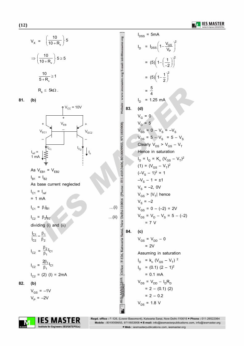
81. (b)
+
–
VEC2
IoI =1 mAref
V = 10VCC
+
–VEB+
–
VEC1
IC1 IC2
As VEB1 = VEB2
IB1 = IB2
As base current neglected
IC1 = Iref
= 1 mA
IC1 = 1B1I …(i)
IC2 = 2 B2I …(ii)
dividing (i) and (ii)
C1 1
C2 2
II
IC2 = 2
C11
I
IC2 = 1
C11
2 I
IC2 = (2) (I) = 2mA
82. (b)
VGS = –1V
VP = –2V
IDSS = 5mA
ID = 2
GSDSS
P
VI 1V
= 2
1(5) 12
= 21(5) 1
2
= 54
ID = 1.25 mA
83. (d)
VG = 0
VD = 5
VGS = 0 – VS = –VS
VDS = 5 – VS = 5 – VS
Clearly VDS > VGS – VT
Hence in saturation
ID = IQ = Kn (VGS – VT)2
(1) = (VGS – VT)2
(–VS – 1)2 = 1
–VS – 1 = ±1
VS = –2, 0V
VGS > |VT| hence
VS = –2
VGS = 0 – (–2) = 2V
VDS = VD – VS = 5 – (–2)
= 7 V
84. (c)
VGS = VDD – 0
= 2V
Assuming in saturation
ID = kn (VGS – VT) 2
ID = (0.1) (2 – 1)2
= 0.1 mA
VDS = VDD – IDRD
= 2 – (0.1) (2)
= 2 – 0.2
VDS = 1.8 V

IES M
ASTER
[EE], ESE-2019 PRELIMS TEST SERIES PAPER-II (TEST-07) (13)
VDS VGS – VT
Hence our assumption of considering insaturation is correct.
85. (b)
nk = µn cox
= n ox
ox
( )t
= 4 12
10(500 10 ) 8.85 10 3.9
100 10
= 5 × 8.85 × 3.9 × 10–6
= 172.57 µA/V2
86. (c)
VGS – VTN = 2 – 1 = 1V, VDS = 0.1 V (given)
VGS – VTN > VDS
transistor is in linear region.
id = kn [2(VGS – VT) VDS – VDS2]
id = 2nGS T DS DS
k W 2 V V v v2 L
id = 6
280 10 10 2 2 1 0.1 0.12 1
id = 6800 10 0.2 0.01
2
id = 6800 0.19 10 76 A
2
87. (c)
Segmentation is a process in which memory isdivided into groups of variable length calledsegments.
88. (b)
The load instruction is basically used to loadthe contents of a memory location onto aregister.
89. (c)
The data is stored on the disk in the form of acollection of blocks called as sectors.
90. (a)
The LRU in case of the sequential blocks as towaste its one cycle just incrementing thecounters.
91. (b)
In MRU it is assumed that the page accessednow is less likely to be accessed again.
92. (a)
93. (a)
94. (c)
95. (c)
96. (c)
97. (b)
98. (a)
99. (a)
100. (a)
101. (c)
102. (d)
103. (b)
Adding items to a full stack is termed as stackunderflow.
104. (a)
Since queue follows FIFO so new elementdeleted from first.
105. (a)
To check whether there is element in the list ornot.
106. (b)
Total number of elements in the matrix will ber*c
107. (b)
It starts with the first element and continues inthe same row until the end of row is reachedand then proceeds with the next row. C followsrow-major order.
108. (b)
Their property is meant for dynamic allocations.
109. (b)
As the name itself suggests, pre-order traversalcan be used.
110. (d)

IES M
ASTER
(14)
In-order traversal follows LNR (Left-Node-Right).
111. (b)
Level order traversal follows a breadth firstsearch approach.
112. (c)
This is one of the property of max-heap thatroot node must have key greater than itschildren.
113. (c)
For any node child nodes are located at either2*i , 2*i +1 So the parent node could be foundby taking the floor of the half of child node.
114. (a)
Building a min-heap the result will a sorted arrayso the option a is correct .If we change theimplementation strategy option- b is also correct.(First filling the right child rather than left childfirst).
115. (c)
Bubble sort is one of the simplest sortingtechniques and perhaps the only advantage ithas over other techniques is that it can detectwhether the input is already sorted.
116. (a)
117. (a)
It takes more memory as one bit used up tostore the sign.
118. (b)
119. (b)
In Daisy chain mechanism, all the devices areconnected using a single request line and they’reserviced based on the interrupting device’spriority.
120. (d)
The time for which the data is held is largerthan the time taken for propogation delay andsetup time.
121. (b)
A 64 bit system means, that at a time 64 bitinstruction can be executed.
122. (d)
If the source host is the client, the port numberin most cases will be ephemeral port number.
123. (d)
Total length is the 16 bit field which containsthe length of UDP header and the data.
124. (a)
A user datagram is encapsulated in an IPdatagram. There is a field in the IP datagramthe defines the total length. There is anotherfield in the IP datagram that defines the lengthof the header. So if we subtract the length of aUDP datagram that is encapsulated in an IPdatagram, we get the length of UDP userdatagram.
125. (a)
Network layer is mainly used for securitypurpose, so IPsec in mainly operates in networklayer.
126. (b)
In selective repeat window, packet that havelost or corrupted must be sent.
127. (d)
In Virtual circuit networks, each node knowsthe upstream node from which a flow data iscoming.
128. (b)
In the congestion avoidance algorithm, the sizeof the congestion window increases additivelyuntil congestion is detected.
129. (c)
Transport layer is responsible for process-to-process delivery.
130. (a)
The most common method used for thiscommunication is Client/Server.
131. (b)
Packets in this method may be delayed or lost.
132. (b)Firstly, it informs the source that the datagramhas been discarded. secondly, it warns thesource that there is congestion in the network.

IES M
ASTER
[EE], ESE-2019 PRELIMS TEST SERIES PAPER-II (TEST-07) (15)
133. (c)
Ping program is used to find if a host is aliveand responding.
134. (c)
TTL field is decremented by one each time thedatagram is processed by a router.
135. (a)
Offset field specifies where the fragment fits inthe original datagram.
136. (c)
The client in socket programming must knowIP address of Server.
137. (c)
The error in wattmeter reading is,
% Error = tan tan 100 [for lagging load]
= tan tan 100 [for leading load]
So, the wattmeter reads high when the powerfactor is lagging and low when the power factoris leading.
pf = cos
so, magnitude of pf will be high, when is low..
Also, error will be high when the value of tan ,
or simply is high or we can say that error willbe high for low power factor.
138. (c)
A probe is used to connect the CRO to the testcircuit. It increases the input impedance of CRO.
A ‘times 10 proobe’ increases the inputresistance by 10times, and decreases the inputcapacitance by 10 times. so effectively thisprobe increases the input impedance of CROby 10 times.
139. (d)
Reproducibility and repeatability are differentterms.
Repeatability describes closeness of outputreadings when the same input is appliedrepetitively, when instrument, measurementconditions observers, location all are same.
140. (c)
The material used for resistance standard, musthave a low thermo electric emf with copper.
High value of thermoelectric emf increase theerror.
141. (b)
The mutual inductance standards are generallyregarded as primary standards of inductance,as their value can be known with greateraccuracy.
142. (c)
It is possible to design an ammeter or voltmeter,which works on induction principle.
But these type of ammeter and voltmeters areexpensive and less accurate. So, generally onlywattmeters based on induction principle areused.
143. (c)
In a cathode ray tube, when high frequencysignals are to be analysed, post deflectionaccelleration is used to increase the bright nessof the trance which is displayed on the screen.This is beacuse, at high frequencies, in order toobtain high sensitivity, the accelerating voltageis kept low, due to which brightness of the thetrance decreases.
So, to increases the brightness of the trace, weuse post deflection acceleration.
Post deflection acceleration doen’t have anyrelation with deflection sensitivity.
144. (a)In eddy current damping, there is an inducedemf in disc and hence an eddy current, whichinteracts with alternating flux and produce atorque opposite to the direction of motion. Toflow the eddy current, the disc should beconducting in nature.
145. (c)As the power being meaured in a low powerfactor circuit is small and current is high onaccount of low power factor. So, it is absolutenecessary to compensate for the pressure coilcurrent by using compensating coil.
146. (a)CTs are always connected in series. So, its

IES M
ASTER
(16)
primary current is independent of secondarycurrent as
I1 = '2 0I I
If secondary is left open, then '2I becomes
zero and hence, I0 will have to become I1,which is normally very high and may takethe CTs core into deep saturation and dam-aged it permanently.
147. (a)As the core of LVDT is made up of highpermeable core, it gives high sensitivity becauseit will be able to detect the small change ininput. High permeable core also reducesharmonics.
148. (a)
In Zener breakdown mechanism, an increase intemperature increases the energies of thevalence electrons and hence makes it easierfor these electrons to escape from the covalentbonds. Less applied voltage is therefore requiredto pull these electrons from their positions inthe crystal lattice and convert them intoconduction electrons.
Thus, Zener breakdown voltage decreases withincrease in temperature and is said to haveNegative Temperature Coefficient (NTC) ofbreakdown voltage.
149. (b)
Drain current (IDS) has negative temperaturecoefficient. This is because mobility of thecharge carriers decreases with increase intemperature. Due to this, thermal runaway isnot encountered in field-effect transistors.
150. (a)
Reverse saturation current (I0) in a silicon diodeis in the range of nA, whereas that in agermanium diode is in the range of A .
An increase in temperature f rom roomtemperature (25°C) to 90°C, I0 increases to
hundreds of A for a Ge diode, whereas in
silicon diode, I0 rises only to tenths of A .
Thus, silicon diodes are preferred to germaniumdiodes for high temperature operation.