an_overview_of_digital_signal_processing_and_its_applications.pdf
TRANSCRIPT

SIGNALS AND THEIR ORIGIN 1.1A signal refers to any continuous function f ( ) which is a function of one or more variables like time, space, frequency, etc. Some common examples of signals are the voltage across a resistor, the velocity of a vehicle, light intensity of an image, temperature, pressure inside a system, etc., as a function of time, space or any other independent variable. These signals are processed in order to either monitor or control one or more parameters of a system. Detection of the average, RMS or peak values of a parameter, separation between adjacent peaks or zero crossings are examples of some processing carried out on the signal. In some applications, the processing may be done in order to produce another signal which has better characteristics than the original signal. The processing of the signal is carried out effi ciently and with ease if these signals are converted to equivalent electrical voltages or currents using transducers. Hence, the emphasis in this book will be restricted to processing signals in electrical form.
NOISE 1.2Processing of the signal is made complex by the presence of other signals called noise. The noise signals are generated from man made and natural objects. Electrical appliances/machinery, lightening and thunderstorms are some of the sources of noise. In addition to this, any signal which interferes with the detection of the desired signal may be called as an intereference or noise. The fi rst step in signal processing is to combat the effect of noise. When the noise and the desired signal have different characteristics, the signal can be completely separated from the noise before processing the signal further. Even though this step is an overhead, this may be mandatory. Let us consider the following example to illustrate this.
FILTERS AND NOISE 1.3Frequency shift keying is a technique adopted for transmitting binary data from one place to another. For example, the transmitted sinusoidal signal may be chosen to be 1025 Hz or 1225 Hz depending upon whether 0 or 1 is to be transmitted.
1
AN OVERVIEW OF DIGITAL SIGNAL PROCESSING AND ITS APPLICATIONS

2 Digital Signal Processors
On the receiver, the signal frequency is determined in order to decode the transmitted data to be 0 or 1. One of the techniques adopted for determining the frequency (also called frequency detection) is to count the number of zero crossings of the signal in a given period of time. This can be done effi ciently if the transmitted signal is received without noise. However, one of the common noise which appears at the receiver input is the power supply ripple. A noise of 60/50 Hz frequency may appear at the input to the receiver. Alternately, if the receiver site has any high frequency oscillator, it may get leaked through the power supply lines and will appear at the input to the receiver.
Both these types of noise will make the detector to take wrong decisions. However, its performance can be improved if these two types of noise are removed from the received signal before it is fed to detector. This can be achieved by using a low pass fi lter for removing the high frequency signal and high pass fi lter for removing the low frequency power supply ripple. The ideal characteristics of low pass, high pass and band pass fi lters are shown in Fig. 1.1. These fi lters may be constructed using discrete components and their frequency response do not have the ideal characteristics. The ideal fi lters pass the signals in the pass band without any attenuation. The signals in the stop band have infi nite attenuation. The transition from pass band to stop band occurs instantaneously as the frequency of the signal is swept. The frequency at which this occurs is called as the cut off frequency fc. These fi lters by themselves qualify to be called as signal processors as they remove the unwanted frequency components. Additional processing may be required to carry out a particular task like frequency detection.
CORRELATORS 1.4However, separation of the signal from the noise cannot always be achieved using simple fi lters shown above. The desired signal and the interfering noise may both lie in the same frequency range (bandwidth). In this case, the signal may be retrieved from noise by exploiting its behaviour in the time domain. The effect of the interference signal may be minimized by multiplying the received signal with the replica of all possible transmitted signals with suitable delay and then integrating them over one period (for e.g.,1 bit duration in the case of FSK) of the transmitted signal. This operation is called correlation.
H( )f
- 0 Frequency ( )fc fc f
H f( )
- 2f - 1f 0 f 1 f 2 Frequency ( )f
H f( )
(a) Low pass fi lter response (b) Bandpass fi lter response
H f( )
- 1f 0 f1 Frequency ( )f
(c) Highpass fi lter response
Fig. 1.1

An Overview of Digital Signal Processing and its Applications 3
CONVOLUTION AND INVERSE FILTERING 1.5On its transit to the receiver, the transmitted signal may pass through several systems and each of these systems may modify it. The output y(t) of a linear time invariant (LTI) causal system can be expressed as the convolution of the input x(t), with the impulse response h(t) which is given by the expression:
0
( ) ( ) ( ) ( ) * ( )t
y t x h t d x t h tt t t= - =Ú (1.1)
Here ∗ denotes the convolution operation .A system is said to be linear if the superposition principle is true. In other words if y1(t) is the response
to the input x1(t) and y2(t) is the response to the input x2(t), then for any scalar a, b let the response of the system to the input a x1(t) + b x2(t) be y(t). If the system is linear then
y(t) = a y1(t) + b y2(t) (1.2)A system is said to be time invariant if a shift in the input causes a corresponding shift in the output.
In other words if y(t) is the response of the system to x(t), then for a time invariant system the response to the time shifted input x(t – t) is given by y(t – t).
A system is said to be causal if the output at any instant is determined only by its present input and its past input/outputs but not by its future inputs. Only causal system can be realised in practice and this requires the impulse response of the system h(t) to be zero for t < 0
For simplicity and to a good accuracy, the systems can be modelled to be LTI and causal in majority of signal processing applications. However, there are applications such as image processing system where causality is not true.
In order to nullify the effect of a system on the transmitted signal, the received signal may be passed through another system whose transfer function (Laplace transform of the impulse response) is the inverse of the original system. Inverse fi lters and equalisers use this principle.
FOURIER TRANSFORM AND CONVOLUTION THEOREM 1.6The signals may be processed either in the time domain or in the transform domain, e.g., computation of the output y(t) using the convolution integral given by (1.1) is an example of time domain processing. The output may also be computed using transform domain techniques. This can be explained as follows: A signal is said to be of fi nite energy if
2| ( ) | f dt t•
-•
< •Ú (1.3)
Any fi nite energy signal f(t) can be represented using the Fourier transform F(w) given by
( ) ( ) j tF f t e dtww•
-
-•
= Ú (1.4)
f(t) can be obtained from F(w) using the inverse Fourier transform given by
( ) 1 ( )2
j tf t F e dww wp
•
-•
= Ú (1.5)
4 Digital Signal Processors
When the lower limit in (1.4) and (1.5) are 0 and jw is replaced by s, we get the expression for the Laplace transform of f(t) and inverse Laplace transform of F(s) respectively.
Convolution theorem relates h(t), x(t) and the convolved output y(t) to their Fourier and Laplace Transforms. Let the Fourier transform and the Laplace Transform of (x(t), h(t), y(t)) be (X(w), H(w), Y(w)) and (X(s), H(s), Y(s)) respectively.
Then if y(t) = x(t) ∗ h(t) then Y(w) = X(w) H(w) and Y(s) = X(s) H(s).Similarly if Y(w) = A(w) ∗ B(w) then y(t) = a(t). b(t) and Y(s) = A(s) ∗ B(s) fi y(t) = a(t). b(t) As mentioned earlier ∗ denotes the convolution operation. H(s), the Laplace Transform of the impulse
response h(t) of a causal LTI system is called as the transfer function of the system and is given by
( )( )( )
Y sH sX s
= (1.6)
where X(s), Y(s) are the Laplace transforms of x(t) and y(t) respectively. Laplace Transforms have a no. of applications like studying the stability of the system, solving the differential equations and fi nding the initial value and fi nal value of a system.
SAMPLING THEOREM AND DISCRETE TIME SYSTEM 1.7Various signal processing operations explained above can be carried out either directly on the continuous signal or indirectly using the samples of the input signal and impulse responses. Accordingly, they are called as continuous time signal processing and discrete time signal processing respectively. The discrete time signal offers no. of advantages. Firstly, it permits a no. of such signals to be transmitted using the same channel by sending them at disjoint time intervals. This technique is called as the time division multiplexing. However, in order to transmit the information without any loss of information the discrete time signal should satisfy the Nyquist’s sampling theorem which states:
Any signal bandlimited to a maximum frequency of fm can be perfectly reconstructed from its samples if the sampling rate, fs is greater than or equal to 2fm. If fs is equal to 2fm, then it is called the Nyquist rate.
If the sampling rate is less than 2fm, then any signal component fh which is greater than fs/2 by Df (i.e., fh = fs/2 + Df) gets mapped to a frequency fs/2 – Df after sampling and appears as a low frequency signal. This is called as aliasing. To avoid this, either the sampling rate should be chosen to be above Nyquist rate or the sampler should be preceded by a low pass fi lter with cut off frequency, fc = fs/2.
LINEARITY, SHIFT INVARIANCE, CAUSALITY AND STABILITY
OF DISCRETE TIME SYSTEMS 1.8Some of the properties of the continuous time system discussed in Section 1.5 can be extended for the discrete time system as follows: A discrete time system is said to be LSI if the superposition property holds and a shift in the input causes a corresponding shift in the output.
In other words if y1(n) is the response of a discrete time system to the input x1(n) and y2(n) is the response to the input x2(n), then for any scalar a, b let the response of the system to the input a x1(n) + b x2(n) be y(n). Then if the system is linear
y(n) = a y1(n) + b y2(n) (1.7)

An Overview of Digital Signal Processing and its Applications 5
The discrete time system is said to be shift invariant if a shift in the input causes a corresponding shift in the output. In other words if y(n) is the response of the system to x(n), then for a shift invariant system the response to the input x(n – k) is given by y(n – k). A LSI system can also be called as linear time invariant (LTI) system if the shift in the index (e.g., k in N – k) corresponds to a different sampling instant.
A discrete time system is causal if the impulse response sequence h(n) = 0 for n < 0. The system is stable, if a bounded input sequence x(n) i.e a sequence for which | x(n) | < h for all n and any arbitrary h results in bounded output sequence y(n). This is achieved if
0| ( ) |k h k•= < •Â (1.8)
Z TRANSFORM 1.9Analogous to the Laplace transform for the continuous time system, for the discrete time system, unilateral Z transform is defi ned. The unilateral Z transform of a sequence x(n) is denoted as X(z) and is given by
0( ) ( ) n
nX z x n z
•-
== Â (1.9)
Here, z denotes a complex variable.The z transform H(z) of the impulse response sequence h(n) of a causal LSI system is called as the
system function. H(z) can be used to examine the stability of a discrete time system. For a stable system, the magnitude of the poles of H(z) should be < 1. In other words, the magnitude of the points at which the denominator of H(z) becomes zero should be less than 1, in a system with system function H(z) given by
11( )
(1 )H z
az-=-
(1.10)
| a | should be < 1 for the system to be stable.
1.9.1 Additional Properties of z transform
1. Linearity If x(n) and X(z) are z transform pairs (denoted as x(n) ´ X(z)) and y(n) ´ Y(z) then
(a x(n) + b y(n)) ´ (a X(z) + b Y(z))
2. Multiplication by Exponential Sequence If x(n) ´ X(k), then an x (n) ´ X(a–1z)
3. Initial and Final Value Theorems The initial value x(0) and fi nal value x(μ) can be evaluated us-ing the Z transform X(z) as follows:
(0) lim ( )z
x X zƕ
= (1.11)
1( ) lim( 1) ( )
zx z X z
Æ• = - (1.12)

6 Digital Signal Processors
4. Differentiation of X(k) If ( ) ( ) thenx n X z´
( ) ( )dnx n z X zdz
´ -
5. Convolution The convolution sum y(n) of two sequences x(n) and h(n) denoted as x(n) ∗ h(n) is given by
0( ) ( ) ( )
n
ky n x k h n k
== -Â (1.13)
If x(n) ´ X (z), h(n) ´ H(z) and y(n) ´ Y(z) and then (x(n) ∗ h(n) ) ´ X(z) H(z) = Y(z).Similarly (a(n) b(n)) ´ (A(z) ∗ H(z))
6. Shifting Property If X(z) is the z transform of the sequence x(n), then the z transform of the sequence x(n – k) is given by X(z)z – k. This property can be used for solving a difference equation. For e.g., consider the output sequence y(n) of a LSI system expressed in terms of the input sequence x(n) by the difference equation
y(n) = x(n) + a y(n – 1) (1.14)Taking the z transform of each of the terms of (1.14) and using the shifting property Y(z) is given by
Y(z) = X(z) + (az –1) Y(z)Rearranging the terms we get
1( ) 1( )( ) (1 )
Y zH zX z az-= =
- (1.15)
The impulse response of the system can be found by taking the inverse z transform of (1.15). In general, z transform can be used to convert a difference equation into an algebraic equation involving the z transforms of the sequences.
7. The inverse z transform of a sequence can be obtained either using the power series expansion of X(k) or using partial fraction expansion, e.g., if X(z) is given by (1.10), its power series expansion is given by
1 1 2 1 3
0( ) 1 ( ) ( ) ( ) n n
nX z az az az a z
•- - - -
== + + + + = � (1.16)
Comparing this with (1.9), it can be concluded that x(n) = an
Similarly if
1 11( )
(1 )(1 )H z
az bz- -=- - (1.17)
Using partial fraction expansion H(z) can be rewritten as
1 11 1( )
( ) ( )(1 ) (1 )a bH z
a b b aaz bz- -= +- -- - (1.18)

An Overview of Digital Signal Processing and its Applications 7
Comparing (1.18) with (1.10) it can be concluded that
( )( ) ( )
n na bh n a ba b b a
= +- -
(1.19)
Z transform can be used to arrive at effi cient schemes for implementation of discrete time systems. This is considered in Section 1.13.
FREQUENCY RESPONSE OF LTI DISCRETE TIME SYSTEM 1.10The response y(n) of a LTI discrete time system with impulse response h(n) for a complex exponential sequence given by
x(n) = ejnw for – μ < n < μis given by
( )( ) ( ) j n m
my n h m e w
•-
=-•= Â (1.20)
Let H(e jw) be defi ned as
( ) ( )j jm
mH e h m ew w
•-
=-•= Â (1.21)
Using (1.21) in (1.20), y(n) is given by
( ) ( ) ( ) ( ) ( )jn jm jn j j
my n e h m e e H e x n H ew w w w w
•-
=-•= = =Â (1.22)
Hence the complex exponential sequence is the eigen function of the discrete LTI system . Since it corresponds to the sampled sinusoid of frequency w, the response, H(e jw) is called as the frequency response of the system.
Properties
1. H(e jw) can be obtained from the transfer function H(z) by evaluating it at z = e jw. This can be verifi ed by comparing (1.21) with (1.9) .
2. H(e jw) is periodic in w with period equal to 2p. In the sampled data system y(n) actually denotes the value y(t) at the nth sampling instant nTs. The dependence of the sampling frequency on the frequency response can be made clear by replacing w by wTs. Hence for the sampled data system with sampling interval Ts, the frequency response is given by H(e jwTs) and it is periodic with a period of (2p/Ts). Since w is equal to 2pf, when the frequency response is plotted as a function of f, it is periodic with a period of (1/Ts).
3. As H(e jw) is periodic in w with period of 2p, (1.21) can be viewed as the Fourier series expansion for H(e jw) with the Fourier coeffi cients h(n) given by
1( ) ( )2
j j nh n H e e dp
w w
p
wp -
= Ú (1.23)
For real values of h(n), |H(ejw)|, the magnitude of the frequency response is symmetric in the interval (0, 2p) and the phase response is antisymmetric in this interval.

8 Digital Signal Processors
DIGITAL SIGNAL PROCESSING 1.11As mentioned in Section 1.7, one of the advantages of discrete time signal is time division multiplexing. The second advantage of discrete time signal is that they can be digitized and they can be processed either using digital hardware or using software. For the digitization, fi rstly, the discrete time signal which can take any value in the range (–Am, Am) where Am denotes the maximum amplitude of the signal is approximated to one of the 2N levels which is closest to the signal. The approximation error is called the quantisation error and it can be made small by choosing N to be large.
The 2N levels may be chosen to be at equal intervals in the range (–Am, Am) in which case the signal is said to be uniformly quantized. The next step is to represent each of these 2N levels by an n bit number. The number of bits, n is given by log22N. Processing the n bit numbers corresponding to the various samples of the signal is called as digital signal processing. It offers a number of advantages compared to processing the continuous time signal directly. The latter approach is also called analog signal processing if the signal amplitude range is also continuous.
ADVANTAGES OF DIGITAL SIGNAL PROCESSING (DSP) 1.121.12.1 Ease of Processing
One of the requirements in signal processing is to delay the signal by a particular duration. For example in moving target indicator radar, a number of pulses are transmitted one after another and the received signal corresponding to adjacent pulses are to be subtracted. This requires the received signal to be delayed by one pulse repetition interval. For the analog signal processing, this is achieved using acoustic delay line. Increasing or decreasing the delay requires the delay line length to be changed which is cumbersome. On the other hand, for DSP, the samples of the received signal can be stored in memory and they can be read after one pulse repetition interval. Delay can be easily changed without switching in or switching out cables.
1.12.2 Thermal Drift and Reliability
For analog signal processing, circuits consisting of analog components like resistors, capacitors, and op amps are used and their characteristics change with temperature. DSP circuits use digital hardware like adders, multipliers and shift registers whose characteristics show no variation with temperature throughout their operating range. Component aging alters the performance of the analog circuit. For example, the dielectric material of capacitors is particularly prone to aging which changes the impedance and alters the performance. DSP circuits have the same performance throughout their life time.
1.12.3 Repeatability
Component tolerance makes the analog circuit to have different characteristics with different set of components of same nominal value. For example, a resistor with 100 W resistor with 10% tolerance can have any value in the range (90, 110) W. Accordingly, the circuit behaviour cannot be exactly predicted. This problem can be minimised by using components with smaller tolerance. But this increases the system cost as these components are costly. Typical capacitors have a tolerance of 20% or worse. This makes the characteristics of an analog circuit to be poorly repeatable with new set of components with same nominal values. Digital circuits, however, are inherently repeatable.

An Overview of Digital Signal Processing and its Applications 9
1.12.4 Immunity to Noise
In analog signal processing, the signals are allowed to take any value within a particular range and noise can easily alter the magnitude. In DSP, the signals take binary values and for altering a 1 to 0 and vice versa a noise voltage of a large magnitude is required. In digital data transmission, the effect of noise can be completely eliminated by putting repeaters at suitable intervals. However, a repeater used with an analog signal will amplify both signal and noise and will be ineffective in combating the noise.
1.12.5 Programmability
DSP functions can be implemented either using microprocessors/microcontrollers or Programmable Digital Signal Processors. This enables the same hardware confi guration to be reprogrammed to perform a very wide variety of signal processing tasks by loading in different software. In the analog case this would call for rewiring/resoldering.
1.12.6 Some Special Signal Processing Techniques
There are some signal processing techniques that cannot be performed by analog systems. Examples of these techniques are linear phase fi lters, notch fi lters, adaptive fi lters, data compression, errol control coding. In control systems, an example is a deadbeat controller used when a very rapid settling time is required.
DSP IN THE SAMPLE AND TRANSFORM DOMAIN 1.13For a discrete time system, the convolution integral given by eqn. (1.1) reduces to the convolution sum given by
0( ) ( ) ( )
n
ky n x n k h k
== -Â (1.24)
where y(n), x(n) and h(n) are the nth sample of output, input and the impulse response of the LTI causal discrete time system and x(n) and h(n) are assumed to be 0 for n < 0. If x(t) and h(t) are of fi nite duration they may be represented faithfully using M, N samples respectively. In this case the output is also of fi nite duration and can be represented using M+N–1 samples. In other words convolution of two sequences of length M, N results in a sequence of length M+N–1. For fi nding y(n), n+1 multiplications and n additions are required. For large values of n, this may call for signifi cant computational effort; y(n) may be alternately computed using an indirect approach using the transforms of the input and the impulse response. One of the transform that may be used is the Discrete Fourier transform (DFT). The DFT X(k) of a sequence x(n) of fi nite length M, for k = 0, … M–1 is defi ned as
21
0( ) ( )
M j knM
nX k x n e
pÊ ˆ- - Á ˜Ë ¯
== Â (1.25)
The computation of the M DFT coeffi cients X(0), … X(M–1) requires M2 complex multiplications. However, using the Fast Fourier Transform (FFT) algorithm, the no. of multiplications required is
reduced to 2M log M2
.
The inverse DFT (IDFT) is used to fi nd x(n) from X(k) using the expression given by

10 Digital Signal Processors
21
0
1( ) ( )M j kn
M
kx n X k e
M
pÊ ˆ- Á ˜Ë ¯
== Â (1.26)
IDFT can also be computed using FFT.
FAST FOURIER TRANSFORM (FFT) 1.14The direct computation of DFT of a sequence of length N requires N2 complex multiplications. The
number of multiplications can be reduced to 2N log N2
using the FFT algorithm. There are two popular FFT algorithms: Decimation in Time (DIT) algorithm and Decimation in Frequency (DIF) algorithm. These two algorithms are dealt in detail in the literature. For the sake of brevity, one of the algorithms, DIT is presented here.
1.14.1 Decimation in Time Algorithm
The fi rst step in this algorithm is to rearrange the sequence in the bit reversed order. In the bit reversed number representation, the binary pattern corresponding to a particular decimal number is obtained by writing the natural binary equivalent of the number in the reverse order so that the most signifi cant bit of the natural binary number becomes the least signifi cant bit of the bit reversed number and vice versa. Using this rule, it can be verifi ed that the binary equivalent of the numbers 0–15 is as shown in Table 1.1.
Let the input sequence be x(0), x(1) … x (N–1). Let the bit reversed sequence be x1(0), x1(1) … x1(N–1). The computation of FFT involves log N stages of computation.
In the fi rst stage, 2 point DFT of blocks of every consecutive two elements of x1(0) … x1(N–1) is computed and the resulting sequence is denoted as X1(0), X1(1), … X1(N–1) as shown in Fig. 1.3. The manner in which X1(k) is obtained from x1(l), for k,l = 0, 1, … N–1 can be explained using the FFT butterfl y diagram shown in Fig. 1.2. Let WN be given by
Table 1.1 Natural binary numbers and their bit reversed equivalents
Decimal number
Natural binary number
Bit reversed number
Decimal num-ber
Natural binary number
Bit reversed number
0 0000 0000 8 1000 00011 0001 1000 9 1001 10012 0010 0100 10 1010 01013 0011 1100 11 1011 11014 0100 0010 12 1100 00115 0101 1010 13 1101 10116 0110 0110 14 1110 01117 0111 1110 15 1111 1111
WN = e –j(2p/N) (1.27)The multiplication factor WN
K is called the twiddle factor. For the 2 point DFT, the value of k is N and hence the twiddle factor is equal to one.
In the second stage, every consecutive block of 4 elements of X1(0), X1(1) … X1(N – 1) are combined using two FFT butterfl ies. For n = 0, 1, … (N/4 –1), the fi rst butterfl y is formed between the 4nth element
Fig. 1.2 FFT Butterfl y with a twiddle factor of WN
k

An Overview of Digital Signal Processing and its Applications 11
and (4n + 2)th element. The second butterfl y is formed between the (4n +1)th element and (4n + 3)th
element. The twiddle factor for the fi rst butterfl y is WN0. The twiddle factor for the second butterfl y is
WNN/2 .For example, for N = 8, the second twiddle factor becomes W8
4. Let the output of the butterfl ies at the 2nd stage be X2(0), X2(1), … X2(N – 1).
In the third stage, every consecutive block of 8 elements of X2(0), X2(1) … X2(N – 1) are combined using four FFT butterfl ies. For n = 0, (N/8 – 1), the fi rst butterfl y is formed between the 8nth element and (8n + 4)th element. The second butterfl y is formed between the (8n +1)th element and (8n + 5)th element. The third butterfl y is formed between the (8n +2)th element and (8n + 6)th element. The fourth butterfl y is formed between the (8n +3)th element and (8n + 7)th element. The twiddle factor for the kth butterfl y (for k = 1, 2, 3, 4) is obtained as WN
(k–1)N/4. For example, for N = 8, the four twiddle factors are W80,
W82, W8
4, W86 respectively. Let the resulting output of the butterfl ies be X2(0), X2(1), … X2(N – 1).
The procedure can be generalized as follows: At the rth stage of FFT computation, every block of consecutive 2r elements of the output of the previous butterfl ies Xr – 1(0), Xr – 1(1) … Xr – 1(N – 1) are combined using 2r–1 butterfl ies. For m = 0, 1, ... (N/2r – 1), the kth butterfl y is formed between the (2rm + k)th element and (2r m + k + 2r–1)th element.
The twiddle factor for the kth butterfl y is given by
WN(k–1)N/p where p = 2r–1.
Twiddle factors at various stages of FFT computation for N = 4, 8, 16 are given in Table 1.2. The complete FFT butterfl y fl ow diagram for N = 8 is given in Fig. 1.3.
Fig. 1.3 Decimation-in-time FFT fl ow diagram for 8 point FFT
Table 1.2 Twiddle factors the FFT butterfl ies for N = 4, 8 16
N = 4 N = 8 N = 16Stage 2Twiddle factor
1, W42 1, W8
4 1, W168
Stage 3Twiddle factor
1, W82
W84, W8
61, W16
4
W168, W16
12
Stage 4Twiddle factor
1, W162
W164, W16
6
W168, W16
10
W1612, W16
14

12 Digital Signal Processors
Fig. 1.4 Convolution using FFT
1.14.2 Convolution using FFT
The convolution can be done using FFT as shown in Fig.1.4. Let the sequences x(n), h(n) be of length L, M respectively. New sequences x¢(n) and h¢(n) are formed by appending M – 1, L – 1 zeros to x(n) and h(n) respectively at their end. Lengths of both of the sequences become L + M – 1. Let N = L + M – 1. The FFT of both of these sequences are found and the corresponding FFT coeffi cients are multiplied and a new set of coeffi cients are obtained. ie. X¢(0) is multiplied with H¢(0), X ¢(1) is multiplied with H¢(1) and so on. The inverse FFT of these coeffi cients gives the convolution of the sequence x(n) with h(n). The total number of real multiplications required for convolution becomes 4([3N/2] log2(N) + N).
Using the direct approach the number of multiplications required is LM. This can be verifi ed as follows: Let L > M. The fi rst M – 1 outputs (y(0) – y(M – 1) require (1 + 2 + 3 + …. M – 1) multiplications. The last M – 1 outputs (y(n) – y(M + N – 2) require (M – 1 + M – 2 + … 3 + 2 + 1 ) multiplications respectively. The remaining L – M + 1 outputs require M multiplications each. Hence, the total no. of multiplications is given by
2 212 ( 1)2
MM L M M M M LM M M LM-¥ + - + ¥ = - + - + =
For small values of L and M, the direct approach is computationally effi cient. For large values, the FFT approach is effi cient, e.g. for L=M=8, the number of multiplications required using direct, DFT approaches are 64, 444 respectively. For L=M=64, they are 4096, 5888 respectively.
DIGITAL FILTERS 1.15In Section 1.3, the use of low pass and high pass fi lters are illustrated. The fl atness of the amplitude response in the pass band and the sharpness of the transition from pass band to stop band determines the complexity of the fi lter or the no. of components required for building the fi lter. Digital fi lters use the digital hardware like adder, multiplier and shift registers. The design of digital fi lters using the transfer function/impulse response of the analog fi lters has been dealt in detail in several textbooks. (see for e.g., Rabiner, Oppenheim). The digital fi lters can be classifi ed into broadly two types: Finite Impulse response (FIR) fi lters and Infi nite impulse response (IIR) fi lters. FIR, IIR fi lters described below are examples of linear shift invariant system (LSI).
1.15.1 FIR Filters
The output of the FIR fi lter at the nth sampling instant y(n), can be expressed as the function of the present as well as the past (M–1) input samples and the impulse response sequence h(k) as follows:
1 1
0 0( ) ( ) ( )
M M
n k kk k
y n x n k h k x h- -
-= =
= - =Â Â (1.28)

An Overview of Digital Signal Processing and its Applications 13
This is a difference equation of order M. It is also referred to as tapped delay line fi lter with M taps or FIR fi lter with M taps. Comparing (1.28) with (1.13), it can be seen that FIR fi lter is a convolver where the present as well as past M – 1 input samples are convolved with M impulse response coeffi cients. Hence, it can also be called as a convolver. It may be noted that the past M – 1 samples can be obtained by storing them in M – 1 shift registers. Each shift register introduces a delay equal to 1 sampling interval and has a transfer function of z–1.
With this observation a structure for the implementation of the FIR fi lter can be obtained as shown in Fig. 1.5. This is also referred to as the direct implementation scheme as it uses M multipliers and adder for M products. In this case, the minimum sampling interval Tsd is given by
Tsd = TM + (M – 1)TA (1.28a)where TM,TA are respectively the time required for one multiplication, addition respectively. An alternative fi lter given in Fig. 1.6 is obtained by taking the transpose of the fi lter structure given in Fig. 1.5. The minimum sampling time, Tst of the transpose fi lter is given by
Tst = TM + TA (1.28b)The transpose of a fi lter/network is obtained as follows: The direction of the signal fl ow in each
branch of the fi lter is reversed. The branching points are replaced by adders and adders are replaced by branching nodes. The nodes at which the input is fed and the output is tapped are interchanged. The transfer function of the transpose structure is the same as the original structure. However their other characteristics like the effect of inaccuracy due to fi nite number of bits used for representing the numbers in a fi lter (referred to as the fi nite word length effect) will be different. This structure can also be used for serial/parallel convolution as in this case the input data can be fed serially bit by bit and the output can also be obtained serially.
For implementation either in software or hardware another scheme that can be used is shown in Fig. 1.7. This consists of two circulating registers for storing and circulating M numbers, a multiplier and an accumulator consisting of a register and an adder.
In this case, an M tap fi lter requires M clock cycles for computation of each output of the fi lter. If Tc is the clock period, the minimum sampling interval Ts, required for the inputs to this fi lter is given by
Ts = MTc (1.28c)
Fig. 1. 6 Serial/parallel convolver Fig. 1.7 Direct implementation scheme with single multiplier/adder
Fig. 1.5 Direct Implementation scheme for FIR fi lter

14 Digital Signal Processors
Merits and Demerits of FIR Filters
FIR fi lters have a numbers of advantages. They are stable and can be made always realizable with suitable delays. The inaccuracy in the output due to the number of bits used for representation of the input samples and the impulse response sequence is smaller in FIR fi lters than in IIR fi lters. The inaccuracy that results in both FIR and IIR fi lter due to the number of bits used for the representation is referred to as fi nite wordlength effect. For speech processing and data transmission, it is required to have frequency selective fi lters whose magnitude response is fl at and the phase response is linear with frequency in the pass band. Such fi lters are referred to as linear phase fi lters and they can be realised using FIR structure. In this case, the impulse response has even symmetry . For example the impulse response of the N tap linear phase FIR fi lter satisfi es
h(n) = h(N – 1 – n) 0 £ n < (N/2) (1.29)For example, in an 8 tap linear phase FIR fi lter, the impulse response coeffi cients satisfy the
conditions:h(7)=h(0), h(6)= h(1), h(5) =h(2), h(4) = h(3) (1.30)
This reduces the number of multiplications required for computing (1.28) by half. In hardware implementation of the fi lter the number of multipliers required is reduced by half.
Another advantage of the FIR fi lter is that an FIR fi lter can be designed using well proven techniques for any arbitrary frequency response. IIR fi lters can be designed only for four basic types like Low pass (LP), High pass (HP), bandpass (BP), Bandstop (BS) and few others. More general fi lters such as multiband fi lters are diffi cult to design using IIR fi lters but can be designed as FIR fi lters.
One of the limitations of FIR fi lter is the need for large number of taps for obtaining fi lters with sharp cut off characteristics. IIR fi lters require only less no. of taps compared to FIR fi lters. More no. of taps require more hardware resources or more computation time. Another disadvantage is the linear phase fi lter may result in non integral no. of sample delays with frequency and it may not be acceptable in some applications.
1.15.2 Real Time Filtering Using FFT
In real time fi lters, the input samples to be processed arrive periodically. If an M Tap FIR fi lter is used for processing, between every sampling interval M multiplications and M-1 additions are to be performed.
Overlap and Save Method
In stead of processing every sample individually, the input sequence may be segmented into overlapping blocks of subsequences of N samples as shown in Fig. 1.8. The no. of samples overlapping between the adjacent block is chosen to be M – 1. Let us see what happens when the block of N samples are convolved with the impulse response sequence. The fi rst M – 1 outputs would be wrong as we require the present and the past M – 1 samples to compute the
Fig. 1.8 Real time fi ltering using overlapand save method

An Overview of Digital Signal Processing and its Applications 15
output. The outputs corresponding to sampling instants M to N would be correct as all the past samples required are contained in the block. The second block contains the samples N – M + 1 to 2N – M. In this block, the outputs corresponding to sampling instants N – M + 1 to N would be wrong and the outputs corresponding to sampling instants N to 2N – M would be correct. However, the correct outputs corresponding to the instants N – M + 1 to N have been already computed using the fi rst block. Hence, in each block, the fi rst M – 1 outputs may be discarded and the remaining N – M + 1 outputs may be saved. This technique for performing convolution using a block of input samples is called as overlap and save method. The convolution may be effi ciently performed using FFT as shown in Section 1.14.2. The following steps are adopted for this purpose. 1. The impulse response sequence h(n) is appended with N – M zeros and the FFT of resulting
sequence is found. Denote the FFT coeffi cients as H(0) – H(N – 1) 2. The FFT of the N samples in the ith block (xi(0) – xi(N – 1) are found. The FFT coeffi cients are
denoted as Xi(0) – Xi(N – 1) 3. Compute Yi(k) using the relation Yi(k) = Xi(k)H(k) for k = 0 – (N – 1) 4. Compute the inverse DFT of {Yi(0), Yi(1) … Yi(N – 1)} and fi nd yi(k). Discard yi(0) – yi(M – 2)
and save yi(M – 1) to yi(N – 1)
Overlap and Add Method
In this method, the input sequence is segmented into non-overlapping blocks of subsequences of L samples as shown in Fig. 1.9.
The samples of the ith block can be written as
xi(n) = x(n + iL) n = 0,1, … L – 1 (1.31a)The L samples of the ith block are appended with
M – 1 zeros to form a sequence of length N which is a power of 2. Let us denote this as xi¢(n). Xi¢(k), the FFT of this sequence is found. Similarly another sequence h¢(n) of length N is formed by appending L – 1 zeros to h(n). H¢(k), the FFT of this sequence is found. Yi(k) is computed as the product of Xi¢(k) and H¢(k). yi(n) is found by computing inverse FFT of Yi(k). Each output block contains N output samples. Since the input blocks are non overlapping, out of the N outputs, fi rst M – 1 outputs and the last M – 1 outputs would be incorrect as at least one sample from the adjacent block is required to get the correct output for these sampling instants. To fi nd the correct output, the outputs corresponding to ith and (i + 1)th block are aligned as shown in Fig.1.9 such that the last M – 1 outputs of ith block overlaps with fi rst M – 1 outputs of the (i + 1)th block. The overlapping outputs are added column wise to get the correct output. L output samples corresponding to ith block are obtained from the N outputs of ith and (i – 1)th block as follows:
y(iN + k) = y(iN + k) + y(iN – M + 1 + k) for k = 0,1, 2, ... M–2 (1.31b)y(iN + k) = y(iN + k) for k = M – 1, M, … L (1.31c)
1 outputs of previous block added withthe firstM –
M – 1 outputs of previous block andthen saved
h n( ) 0….0
( )x n1
M
Add overlapped output Æ
Final output sequence
L M + 1 outputssaved directly–
Non overlapping input blocks; eachblock is zero-padded by 1 samplesM –
0
( )x n2
( )x n3
( )1 ny ( )2 ny ( )3 ny
0
0
N
N
N
L
+
+
Coefficients vector zero-padded to N
x
Fig. 1.9 Real time fi ltering using overlapand add method

16 Digital Signal Processors
This can be verifi ed by fi nding y(iN + k) for k = 0 and M – 2 as follows
y(iN) = y(iN) + y( iN – M + 1) (1.31d)
y(iN + M – 2) = y(iN + M – 2) + y( iN – 1) (1.31e)
1.15.3 Design of FIR Filters
The FIR fi lter may be specifi ed by the frequency response of the fi lter. This in turn can be specifi ed by the magnitude response and the desired phase response of the fi lter. A number of techniques have been developed for fi nding the fi lter coeffi cients and computer programs have also been developed to facilitate this. Overview of two of the methods the window method and frequency sampling method is presented next.
Window Method Using the periodicity property of the frequency response, it is shown in section 1.10 that h(n) the impulse response coeffi cients can be obtained as the Fourier coeffi cients given by Eqn. (1.23). However, this requires an infi nite sequence and the fi lter will be non causal as h(n) is nonzero for n < 0. This series may be truncated to have N coeffi cients. However this will result in overshoot and ripples in both pass band and stop band and is referred to as Gibb’s oscillation or phenomena. Another problem with the fourier series technique is its slow convergence. Choosing larger values of N does not automatically reduce the magnitude of the ripples in the transition region from pass to stop band signifi cantly. This problem is overcome by choosing a window sequence w(n) and multiplying it with h(n) obtained using the Fourier series approach. w(n) is chosen so as to obtain a smooth transition from the pass band to the stop band and to be non-zero for 0 £ n £ N – 1. The resulting hw(n) is made causal by shifting it by (N – 1)/2 towards right. Some of the window functions used are the rectangular window, Von Hann (also referred to as Hanning) window, Hamming window, Blackman window and kaiser window. The expressions for the fi rst three windows can be specifi ed using the parameter a as follows:
w(n) = a + (1 – a)cos 21
nN
pÊ ˆÁ ˜Ë ¯-
for 0 £ n £ N – 1 (1.32)
= 0 otherwise.The value of a is 1, 0.5, 0.54 respectively for rectangular, Hanning, Hamming windows. The
Blackman window function is also of similar form and is given by
w(n) = 0.42 – 0.5 cos 21
nN
pÊ ˆÁ ˜Ë ¯-
+ 0.08 cos 41
nN
pÊ ˆÁ ˜Ë ¯-
for 0 £ n £ N–1
= 0 otherwise. (1.33)The frequency response of the window functions have a main lobe and a no. of side lobes. The ripple
ratio defi ned as the ratio of the fi rst side lobe amplitude to the main lobe amplitude in the frequency response of the window function increases with a and the main lobe width decreases with a.
Frequency Sampling Method In this method the value of the frequency response at M points in the interval (0, (2p/Ts)) is taken. In other words H(e jwTs) is evaluated for w = (2pk/MTs) for 0 £ k £ M – 1 and are taken to be M DFT coeffi cients. The inverse DFT of this sequence is taken and is treated as M impulse response samples h(n). Out of these M samples N samples (N < M) is taken to be the impulse response sequence for the FIR fi lter with N taps. To minimize the Gibb’s oscillations, this is combined

An Overview of Digital Signal Processing and its Applications 17
with one of the window functions discussed in the last section. The choice of the value of N may be done iteratively. Starting with a value of N, the fi lter frequency response may be evaluated after windowing. If it differs signifi cantly from the desired frequency response, the value of N may be changed. This step is repeated till a satisfactory response is obtained. Several variations of the frequency sampling method is used in practice. For example, instead of choosing all the M DFT coeffi cients using the frequency response, some of the coeffi cients in the transition region from pass band to the stop band may be chosen using optimization techniques in order to achieve the required ripple as well as undershoot/overshoot characteristics.
1.15.4 IIR Filters
The output of the IIR fi lter at the nth sampling instant y(n), can be expressed as the function of the present input and past M-1 input samples as well as the past N – 1 output samples and is given by :
1 1
0 1( ) ( ) ( ) ( ) ( )
M N
k ky n x n k a k y n k b k
- -
= == - + -Â Â (1.34)
where a(k) and b(k) are weight factors for the inputs and past outputs. For ease of notation, the samples are represented using suffi xes wherever convenient. In terms of this notation, (1.34) can be written as
1 1
0 1
M N
n n k k n k kk k
y x a y b- -
- -= =
= +Â Â (1.35)
Since the present output depends on the past outputs, IIR fi lter is also called as a recursive fi lter. The Z transform of (1.34) can be used to arrive at different structures for implementation of the fi lter. For M = N and b(0) = 1, the transfer function H(k) of the fi lter given by (1.34) is
( ) ( )( )( ) ( )
Y z A zH zX z B z
= = (1.36)
1 2 3 2 10 1 2 3 2 1
1 2 3 2 11 2 3 2 1
... ( )
1 ...
N NN N
N NN N
a a z a z a z a z a zH z
b z b z b z b z b z
- - - - + - +- -
- - - - + - +- -
+ + + + +=
+ + + + + (1.37)
where A(z), B(z) are the z transform of the weights a(k) and b(k). Structure for implementation of the fi lter by given (1.34) – (1.36) is shown in Fig. 1.10. It is called as the direct implementation structure. It can be verifi ed that the top set of adders and delay units with transfer function z –1 realises the function A(k) and the bottom units realise the function 1/B(z). Transpose of this fi lter is shown in Fig. 1.11. Both of these fi lter structures require 2(N – 1) delay units, 2(N – 1) adders and 2N – 1 multipliers. The number of delay units can be reduced by realising 1/B(z) fi rst and feeding the output of this fi lter to the fi lter with transfer function A(z) as shown in Fig. 1.12. Since the delay units in both of these fi lters have the same
Fig. 1.10 Direct implementation structure for an IIR fi lter

18 Digital Signal Processors
inputs, a single delay unit can be shared by both of the fi lters with the transfer function 1/B(z) and A(z). The resulting fi lter structure is given in Fig. 1.13. A digital fi lter is said to be canonic if the no. of delay units is equal to the order of the transfer function. Since in the above case, the order of the transfer function is N – 1 and the number of delay units used in Fig. 1.13, the fi lter given by Fig. 1.13 represents a canonic realization. Several other realizations can be obtained by factorizing H(z) or writing it as a sum of a number of transfer functions.
Accordingly a cascade realisation and parallel realisation of the fi lters are obtained.
As mentioned earlier an IIR requires less hardware and computational effort compared to FIR fi lter for the same sharpness and fl atness in the fi lter. However, these fi lters may not always be realisable and may become unstable and are affected more by the fi nite word length effects. When an IIR scheme exists for an FIR fi lter, then it requires less memory and less computation time compared to the latter. For example consider an FIR fi lter with M coeffi cients in which the nth
coeffi cient is given by h(n) = an (1.38)
The transfer function of this fi lter can be written as
H(z) = 1+ (az–1) + (az–1)2 + (az–1) (M – 1) (1.39a)
1
11 ( )
1
Mazaz
-
--=
- (1.39b)
(1.39a) represents an FIR fi lter and it requires M – 1 delay units, M – 1 adders as well as multipliers. (1.39b) represents an equivalent IIR fi lter. This requires M + 1 delay units, two adders and two multipliers.
Fig. 1.11 Direct implementation scheme for the IIR Fig. 1.12 An alternate implementation scheme fi lter using the transpose structure for the IIR fi lter
Fig. 1.13 Canonic realisation scheme for the IIR fi lter

An Overview of Digital Signal Processing and its Applications 19
1.15.5 Design of IIR Filters
Design of analog fi lters for LP. HP, BP, and BS has been studied in detail in the past and has been implemented in a large number of communication and consumer electronic circuits. The impulse response of the IIR fi lters can be obtained from the corresponding analog circuits commonly using one of the techniques impulse invariance method and the bilinear transform method. These two techniques are discussed in brief next.
1.15.6 Impulse Invariance Method
In this method, a digital IIR fi lter with impulse response h(n) is obtained from the analog fi lter with impulse response ha(t) by evaluating h(n) as
h(n) = ha(t) for t = nTs ; N = 0,1,2 (1.40a)where Ts is the sampling interval. However this method is applicable only if the analog fi lter response is bandlimited such that the frequency response H(jw) is given by
H(jw) = 0 for | w | > 1/2Ts (1.40b)If this condition is not satisfi ed, aliasing occurs; i.e., the signal with frequency f, in the frequency
range 1/2Ts to 1/Ts gets mapped to (f – 1/2Ts). Because of periodic nature of the frequency response of the LTI digital fi lters, for m = 1, 2, …, all the signals in the frequency range (m/Ts, (2m + 1)/2Ts) gets mapped to the frequency range (0, 1/2Ts) in the digital fi lters. The signal with frequency f in the range((2m + 1)/2Ts, (2m + 2)/2Ts) appears as f – 1/2Ts due to aliasing. Hence eventhough this method is simple it is not applicable for fi lters whose response is not bandlimited. For example, this method is not suitable for the design of high pass fi lters. In practice, this method can be adopted if
H(jw) < 0.01 Hmax for | w | > 1/2Ts (1.40c)where Hmax denotes the maximum amplitude of the frequency response of the analog fi lter in the frequency range (0, 1/2Ts).
1.15.7 Bilinear Transform Method
In this method the transfer function H(z) of the digital fi lter is obtained from the corresponding analog fi lter transfer function H(s) by using the mapping given by
H(z) = H(s) with1
12 1
1s
zsT z
-
-
Ê ˆ-= Á ˜+Ë ¯ (1.41)
The relationship between the digital frequency w and the analog frequency Ω can be obtained by substituting s = jW and z = ejwTs in (1.41) as follows:
2 11
j Ts
j Tss
ejT e
w
w
-
-
Ê ˆ-W = Á ˜+Ë ¯ (1.42)
W = (2/Ts) tan (wTs/2) (1.42a)In this case the upper half of the imaginary axis (or in other words the frequency range (0, μ) is
mapped uniquely within the unit circle corresponding to the z transform. Hence, aliasing does not occur in this case. However, this method introduces distortion in the frequency response of the digital fi lter

20 Digital Signal Processors
designed. Specifi cally, the phase response of this fi lter is distorted and hence a fi lter with linear phase characteristics cannot be obtained using the bilinear transform method.
This is because the bilinear transform results in nonlinear mapping between the the digital frequency w and the analog frequency W as given by (1.42a). This is called as frequency warping.
To overcome this nonlinearity, compensation has to be applied to the fi lter. One of the technique adopted is to prewarp the cutoff frequencies of the fi lter.This is called as prewarping. For example, if a digital fi lter with the cut off frequencies in the pass band as w1, w2, w3, w4 is desired, an analog fi lter with cut off frequencies given by
Wi = (2/Ts) tan (wi Ts/2) for i = 1, 2, 3,4 (1.42b)is designed. After the warping given by (1.42a), a digital fi lter with the desired cut off frequencies is obtained. The prewarping can only compensate for the amplitude nonlinearities and the phase nonlinearities cannot be overcome.
FINITE WORD LENGTH EFFECT IN DIGITAL FILTERS 1.16Due to fi nite size of the registers used for storing the output of the processing elements like adders and multipliers, overfl ow can occur in FIR fi lters if the results exceed the capacity of the registers. These results will normally be rounded off and this gives rise to round off noise. Overfl ow can be avoided by using fl oating point arithmetic. However, in fi lters using fi xed point computations, the overfl ow can be minimized by scaling the impulse response coeffi cients suitably.
In the case of IIR fi lters, because of the feed back connection, fi nite precision arithmetic can lead to oscillations which make the output to keep alternating between two values. Such oscillations are called as limit cycle oscillations. This can occur when the input to the fi lter is zero for example during silence periods in voice communication. In this case the output keeps oscillating between two small values and is referred to as zero input limit cycles. Another type of oscillation called as overfl ow limit cycle oscillation occurs when overfl ow occurs at the output due to the fi nite precision arithmetic. In this case output can keep oscillating with amplitudes equal to the full supply voltage. Another effect of fi nite word length is the quantization noise. It can arise due to inadequate no. of bits for representing the input to the fi lter, output of the fi lter or the output of the processing elements like multipliers and adders.
POWER SPECTRUM ESTIMATION 1.17Power spectrum of a stationary signal may be obtained by considering a block of N samples and computing the FFT of these samples. Power spectrum or periodogram is defi ned as
2 *1 1( ) ( ) ( ) ( )P k X k X k X kN N
= = (1.43a)
where X(k) is the FFT of the input sequence. When the length of the data sequence is large, the power spectrum is estimated by segmenting the data sequence into a number of overlapping segments. Figure 1.14 shows the most commonly used method for the power spectrum estimation using the Welch method. In this method, the averaged periodogram is obtained by segmenting the input into blocks of N samples and multiplying them with a bell shaped window w(n) to reduce spectral leakage. The accuracy of the averaged spectrogram can be increased by increasing the number of samples, M, overlapping between consecutive blocks. Typically M is chosen to be N/2. K, the total number of segments of data sequence of length L is given by

An Overview of Digital Signal Processing and its Applications 21
int 1L NKM-Ê ˆ= +Á ˜Ë ¯ (1.43b)
where int(.) is the integer operator. For each of the windowed segment, N point FFT is found and the Power spectrum corresponding to the ith segment is denoted as Pi(k) and is given by
21( ) ( )i iw
P k X kNP
= (1.43c)
Long data sequence ( ) of lengthx n L
x n1( )
x n2( )
x nN( )
N
M
P k1( ) = Ω ΩX k1( )21
––NPw
P k2( ) = Ω ΩX k2( )21
––NPw
P kN( ) = Ω ΩX kN( )21
––NPw
Fig. 1.14 Computation of power spectrum using Welch algorithm
This includes the contribution due to the window function. Power of the window function is denoted as Pw and is given by
12
0
1( ) ( )N
wn
P k w nN
-
== Â (1.43d)
The averaged power spectrum of the entire data sequence is denoted as P(k) and is given by
2
1
1( ) ( ) 0,1,2, ... 1K
iiw
P k X k k NNKP =
= = -Â (1.43e)
Compared to the periodogram obtained using a single window of length L, the computation of periodogram using Welch method (given by (1.43e)) results in more accurate and smoother estimate of power spectrum. Size of the window N has to be chosen as a compromise between accuracy and frequency resolution: Smaller N results in poor frequency resolution but better accuracy; the reverse is true for larger N.
SHORT TIME FOURIER TRANSFORM 1.18Many real world signals such as speech, radar and sonar signals are non stationary in nature. Their frequency, phase and peak amplitude may vary with time. For example, the chirp signal, also referred to as linear frequency signal (LFM), given by
x[n] = A cos (w0n2) (1.44a)is used in continuous wave radar to determine the range of a target. In this signal, the frequency of the signal linearly increases over a time period. Similarly, the frequency components in the speech signal

22 Digital Signal Processors
varies from time to time. In order to evaluate the frequency content of a signal as a function of time, short time fourier transform (STFT) may be used.The STFT of a sequence x[n] is defi ned by
STFT ( , ) [ ] [ ]m
j j m
mX e n x n m w m ew w
=•-
=-•= -Â (1.44b)
w[m] is a window sequence. The width of window is chosen so that the signal may be considered to be stationary in that interval. When w[n] is rectangular window, the resulting transform is called as the discrete time fourier transform (DTFT).
In practice, the window sequence of fi nite length R is chosen. Moreover, the STFT is evaluated at N
(N ≥ R) equi-distant points along the unit circle 2 kNp . The sampled values of the STFT is denoted as
2
STFT STFT 2 STFT( , ) ( , ) ,j kj N
kN
X k n X e n X e np
wpw =
Ê ˆ= = Á ˜
Ë ¯ (1.44c)
1
0
2 km[ ] [ ] 0 1
m R
m
j Nx n m w m e k Np= -
=
-= - £ £ -Â (1.44d)
From (1.44d), it may be noted that XSTFT [k,n] may be obtained by fi nding DFT of x[n–m]w[n].XSTFT [k,n] is periodic with respect to k with period N. Assuming w[m] to be non zero, x[n–m] can be obtained by computing the inverse DFT of XSTFT [k,n] and is given by
1
STFT0
21[ ] [ , ] 0 1
[ ]
N
k
j kmNx n m X k n e m Rw m N
p-
=- = £ £ -Â (1.44e)
As XSTFT [k,n] is a function of 2 variables, it requires a three dimensional plot. In practice, a two dimensional plot known as spectrogram is used to plot XSTFT [k, n]. In this plot, the X and Y axis denote the time sample index and frequency sample index respectively. The magnitude of XSTFT [k, n] is indicated by the darkness of the point. Higher the darkness, higher is the amplitude of XSTFT [k,n].
The characteristics of the window function determine the time resolution (Dt) and frequency resolution(Dw). If R is small, the window duration is small and STFT has very good time resolution. Two signals of the same frequency but occurring one after another with a delay of Dt can be perceived as two different signals in the STFT plot. However, small R implies small N and the frequency resolution 2Np
becomes poor. On the other hand, large window duration results in better frequency resolution but poor time resolution.
MULTIRATE SIGNAL PROCESSING 1.19Multirate signal processing refers to the techniques adopted for processing a digital signal by sampling it further either using a higher rate than the rate at which the digital samples were obtained or using a lower sampling rate. The sampler used for this purpose is accordingly called as upsampler, downsampler respectively. The down sampler is also referred to as a decimator and a decimator which downsamples the input by a factor of M is denoted by the symbol given in Fig. 1.15.a. The upsampler is also referred to as interpolator and an interpolator which increases the sampling rate by a factor of M is denoted by

An Overview of Digital Signal Processing and its Applications 23
the symbol given in Fig. 1.15.b. If xd(n) denotes the output of an M factor decimator of an input signal x(n), then xd(n) can be written as
xd(n) = x(Mn) for N = 1, 2, 3, … (1.45) Similarly if yu(n) denote the output of an M factor interpolator of a signal y(n), yu(n) is given by
yu(n) = y(n/M) for n = 0, M, 2M, 3M … (1.46) = 0 otherwise
1.19.1 Frequency Domain Characterization of the Decimator and Interpolator
The frequency domain characterization of the decimator and interpolator can be obtained using the z transform of xd(n) and yu(n) denoted as Xd(k) and Yu(k) respectively.
( ) ( ) ( )n nd d
n nX z x n z x Mn z
• •- -
=-• =-•= =Â Â (1.47a)
1 2 3(0) ( ) (2 ) (3 )x x M z x M z x M z- - -= + + + + � (1.47b)Let us defi ne an intermediate sequence xa(n) as follows:
xa(n) = x(n) for n = kM; k = 0, 1, 2, …. (1.47c) = 0 otherwise
xa(n) can be rewritten as
xa(n) = x(n)c(n) (1.47d)where c(n) is a periodic sequence with period M and is defi ned as:
c(n) = [1, 0, 0, 0, … 0] (1.47e)C(k), the DFT of c(n) is given by
C(k) = 1 for k = 0, 1, 2, …. M–1 (1.47f)
Computing the inverse DFT of C(k) and denoting 2jMep-
by the symbol WM we get
10
1( ) M knMkc n W
M- -
== Â (1.47g)
Substituting eqn (1.47g) in (1.47d), Xa(k) can be obtained as
10 0
1( ) ( )knMn
a Mn kX z x n z WM
-• --= == Â Â (1.47h)
1
0 01 ( )M kn n
Mk n W x n zM
- • - -= == Â Â (1.47i)
1
0 01 ( )( )M k n
Mk n x n W zM
- • -= == Â Â (1.47j)
1
01 ( )M k
Mk X W zM
-== Â (1.47k)
Fig. 1.15 (a) Downsampler; (b) Upsampler

24 Digital Signal Processors
Using (1.47c) in (1.47b), Xd(k) can be rewritten as 1 2 3( ) (0) ( ) (2 ) (3 )d a a a aX z x x M z x M z x M z- - -= + + + + � (1.47l)
For M = 2, Xd(k) is given by 1 2 3( ) (0) (2) (4) (6)d a a a aX z x x z x z x z- - -= + + + + � (1.47m)
Since xa(1), xa(3), xa(5) ... are zero, Eqn. (1.47m) can be rewritten as 1 2 3 42 2 2 2
1 12
( ) (0) (1) (2) (3) (4)d a a a a a
Ma a
X z x x z x z x z x z
X z X z
- - - -= + + + +
Ê ˆ Ê ˆ= =Á ˜ Á ˜
Ë ¯ Ë ¯
�
(1.47n)
Using (1.47k) in (1.47n), we get 1
10
1 ( ) M k Md kX z X W z
M-
=
Ê ˆ= Á ˜
Ë ¯Â (1.47o)
Similarly, Yu(k) can be written as follows:
( )
( )
, , 0,1,2, ...
2 3
( )
(0) (1) (2) (3)
n nu u
n nn kM k
M M M
M
nY z y n z y zM
y y z y z y z
Y z
• •- -
=-• =-•= =
- - -
Ê ˆ= = Á ˜Ë ¯
= + + + +
=
 Â
�
(1.48)
1.19.2 Spectrum at the Output of the Downsampler and Upsampler
More insight into the downsampling and upsampling process can be gained by looking at the spectrum of the sampled signal and comparing it with the spectrum of the original signal.
Frequency spectrum at the output of the decimator and interpolator can be obtained by substituting z = e–jw in (1.47o) and (1.48). For M =2, the frequency response of the decimator and interpolator are given by (1.49) and (1.50).
/2 /21( ) [ ( ) ( )]2
j j jdX e X e X ew w w- -= + (1.49)
Yu(z) = Y(e–j2w) (1.50)
Let H(w), denote the frequency spectrum of a signal bandlimited to fm. Hs(w) denotes the spectrum at the output of sampler which samples the analog input at the rate of fs samples/sec. Xd(w) denotes the frequency spectrum at the output of the downsampler which samples the output of the above sampler at the rate of fd (i.e., fs/M) samples/sec. Yu(w) denotes the frequency spectrum at the output of the upsampler which samples the output of the above sampler at the rate of Mfs samples/sec.
For the case, where the input signal is assumed to be a low pass signal bandlimited to wm = 0.4p radians and M = 2, the spectrum of H(w), Hs(w) and Hd(w) and Hu(w) are shown in Fig. 1.16(a), Fig. 1.16(b), Fig. 1.16(c). and Fig. 1.16(e) respectively.

An Overview of Digital Signal Processing and its Applications 25
–0.4p 0.4p
Fig. 1.16(a) Spectrum of the input signal
–4p –3p –2p –p 0 p 2p 3p 4p 5p
Fig. 1.16(b) Spectrum of the sampled signal w
–4p –3p –2p –p 0 p 2p 3p 4p 5p
Fig. 1.16(c) Spectrum at the decimator output for M =2 and wM =0.4p
–4p –3p –2p –p 0 p 2p 3p 4p 5p
Fig. 1.16(d) Spectrum at the decimator output for M=2 and wM = 0.6p
–4p –3p –2p –p 0 p 2p 3p 4p 5p
Fig. 1.16(e) Spectrum at the interpolator output for M =2 and wM = 0.4p
In Fig. 1.16(b). the frequency spectrum given in Fig. 1.16(a). gets replicated at intervals of 2p radians. Fig. 1.16(c) is obtained by stretching the frequency spectrum of the sampled signal by a factor of two along the w axis and replicating it at intervals of p radians. The magnitude of the spectrum is scaled by a factor of 2. Spectrum at the output of the interpolator is shown in Fig. 1.16(e). This is obtained by compressing the frequency spectrum of the sampled signal by a factor of two along the w axis and replicating it at intervals of p radians. It may be noted that a signal which is sampled and decimated by 2 can be recovered by interpolating it by 2 and passing it through a low pass fi lter with cutoff frequency of wm = 0.4p. Similarly, a signal which is sampled and upsampled by 2 can be recovered by decimating it by 2 and passing it through a low pass fi lter with cutoff frequency of wm = 0.4p.
It can be verifi ed from Fig. 1.16(c) that the band of signals centred around 0 radians and its replicas at intervals of p radians will be non overlapping only if wm £ 0.5p radians. Fig. 1.16(d) shows the spectrum at the output of the decimator when wm = 0.6p radians. In this case, the replicas at intervals of p overlap

26 Digital Signal Processors
and aliasing is said to occur. In this case, the original signal cannot be faithfully recovered from the decimated signal by passing it through an interpolator and a low pass fi lter.
In general, in order to avoid the aliasing, the input to the decimator should be bandlimited to p/M. A low pass fi lter, also referred to as antialiasing fi lter, with cut off frequency wc = p/M is used for this purpose.
1.19.3 Subband Coding
Processing a signal after downsampling or upsampling has a no. of advantages. To appreciate it let us consider the example of a voice coder/decoder. When an analog signal is digitized using the sampler followed by the quantizer, the minimum sampling rate required is determined by the maximum frequency component in the signal and the no. of bits used for quantisation is independent of the relative importance of the various frequency components that constitute the signal. Nonuniform quantizers allocate different step sizes for different amplitude ranges of the signal taking into account their probability of occurrence. Low amplitude signals occur more frequently and are more important. They are allocated small step sizes. Large amplitude signals are quantized with large step size.
Quantisation noise and the bit rate required for digitizing an analog signal can be reduced further by examining their frequency content and allocating the no. of bits per sample depending upon their importance. For example, the energy in the speech signal is concentrated more in the low frequency region of (0–1 kHz) and is of decreasing concentration as the frequency is increased. Hence, more number of bits may be allocated in frequency bands where there is more energy concentration and less number of bits may be allocated where there is less concentration. This technique is called as the subband coding. The fi rst step required for subband coding is to separate the incoming signal into separate bands using low pass, band pass and high pass fi lters. This may be done in the digital domain; i.e., the analog signal may fi rst be sampled and quantized without any regard to the frequency. The resulting digital signal may then be passed through the digital fi lters to separate the different band of frequencies. The individual band of frequencies may be individually processed further. However they need not be processed at the rate at which the analog signal was sampled. This can be be verifi ed using the sampling theorem for the bandpass signal.
1.19.4 Sampling Theorem for Bandpass Signals and its Application
Bandpass Sampling Theorem A band pass signal can be faithfully reproduced from its samples if it is sampled at the rate fs = 2(f1–f2) = 2B if either f1 or f2 is a harmonic of 2B. Here, f1 and f2 denote the lowest and highest frequency components of the signal respectively. B denotes the bandwidth. If neither f1 nor f2 is a harmonic of 2B, then fs is chosen to be greater than 2B such that this condition is satisfi ed. In general, the range of fs required for a bandpass signal is 2B £ fs £ 4B
In the above subband encoder, if one of the subband is of bandwidth 0.5 kHz, it need not be sampled at 8 kilosamples/s(KSPS) for further processing but a sampling rate of 1KSPS may be just adequate. In practice, one may choose 2 KSPS as the sampling rate. When the voice signal is sampled at 8 KSPS rate, at the output of the fi lter corresponding to a sub band, the samples depart at 8 KSPS rate, but all of these samples are not required for processing. In the above case only 1/4th of the samples may be retained and the rest of them may be discarded. This is achieved using a down sampler.
At the receiver, the decoder has to combine the outputs from the individual sub bands and deliver a single contiguous band. Even though the individual bands generate samples at a rate lower than 8 KSPS the signal has to be delivered at the 8 KSPS rate to the play out device. This is achieved by sampling the

An Overview of Digital Signal Processing and its Applications 27
output of the sub band at a rate higher than the rate at which the sample arrive at its input. This is achieved by inserting zeros between the actual sample values. This process is achieved by the upsampler.
1.19.5 Block Diagram of a Subband Processing System and Filter Banks
The block diagram of a subband processing system which processes M subbands individually using decimation by M and then upsampling by M is shown in Fig. 1.17. The fi lters H1(k), H2(k) … HM(k) denote the fi lters used for separating the M bands and are called as analysis fi lter banks. When the bandwidth of each of the fi lter band is the same, each of them can be decimated by a factor of M or lower without causing aliasing. In this case the fi lter banks are called as the decimated fi lter banks. If the decimation factor is M, then they are called as maximally decimated fi lter banks and they result in the maximum computational effi ciency. The fi lters G1(k), G2(k), … GM(k) are called as the synthesis fi lter banks. The analysis and synthesis fi lter banks shown in Fig. 1.18 require narrow bandpass fi lters. The design of the analysis fi lter banks can be simplifi ed by using the tree structure given in Fig. 1.18. The corresponding tree structure for the synthesis fi lter bank is shown in Fig. 1.19. These structures use only the low pass and high pass fi lters. The cutoff frequency of the low pass fi lter is increased as the tree is traversed towards the right. In Fig. 1.18 H0(k), H1(k) denote the transfer function of the low pass, high pass fi lter respectively and it can be verifi ed that
H Z1( ) Ø M
H Z2( )Ø M
H ZM( )Ø M
SUB
BAND
PROCESSOR
G Z1( )≠ M
G Z2( )≠ M
G ZM( )≠ M
yn
x n( )
H Z0( ) Ø 2
x n( )
H Z00( ) Ø 2
Ø 2
H Z1( )
Ø 2
Ø 2
Ø 2
H Z01( )
H Z10( )
H Z11( )
y n0( )
y n1( )
y n2( )
y n3( )
Fig. 1.17 A subband processor with fi lter banks Fig. 1.18 Tree structured analysis fi lter bank
H0(k) = H1(–z) (1.51)The two channel fi lter bank which satisfi es(1.51) is
referred to as a quadrature mirror fi lter bank (QMF). The tree structure is obtained by splitting every
branch into two. However it may not always be required to split each branch into two for subband processing. For eg. in the subband coding scheme proposed by Crochiere[1983], the analog speech signal is sampled at 8 KSPS and split into 4 bands as shown in Fig. 1.19(a). Each of these bands has a bandwidth of 1 kHz. Next the band 0–1 kHz is split into 2 bands and a pruned tree with 5 bands: 0–0.5, 0.5–1, 1–2, 2–3 and 3–4 kHz is shown in Fig. 1.19(a)
G Z00( )
≠2
y n0( )
y n1( )
y n2( )
y n3( )
+
+
≠2
≠2
≠2
G Z01( )
G Z10( )
G Z11( )
≠2
≠2
G Z0( )
G Z1( )
x n( )+
Fig. 1.19 Tree structured synthesis fi lter bank

28 Digital Signal Processors
and coded individually. Quantization of the fi rst two bands with 5 bits/sample, the next two bands with 4 bits/sample and the last band with 3 bits/sample gives a bit rate of 32 kbps. Quantization of the fi rst two bands with 4 bits/sample, the next two bands with 2 bits/sample and the last band with 0 bits/sample gives a bit rate of 16 kbps. With the 8 KSPS sampling 8 bits/samples, the bit rate required is 64 kbps. Hence the decimation/interpolation has facilitated the data compression by a factor of 2–4.
H Z0( ) Ø 2
H Z00( ) Ø 2
Ø 2
H Z1( )
Ø 2
Ø 2
Ø 2
H Z01( )
H Z10( )
H Z11( )
y n2( )
y n3( )
H Z000( ) Ø 2
Ø 2H Z001( )
0-2kHz
4K
SP
S4
KS
PS
2K
SP
S
0-0.5kHz
2-3kHz
3-4kHz2
KS
PS
2K
SP
S
1K
SP
S
1-2kHz
0.5-1kHz
2-4kHz
8K
SP
S
0 – 1 kHz
Fig. 1.19(a) Subband encoder
1.19.6 Reuse of Digital Filters for Different Subbands
One of the important characteristics of digital fi lters is that the cut off frequency of the fi lter cannot be uniquely determined from the fi lter architectural diagram and the impulse response response coeffi cients. For example, the cut off frequency of the M tap FIR fi lter shown in Fig. 1.4 cannot be uniquely determined if the impulse response coeffi cients h0, h1, …hM–1 are specifi ed. This is because, cut off frequency normalized by the sampling rate is used for the design of digital fi lter. Hence, a low pass fi lter with cut off frequency of 0.2p radians has the cut off frequency of 1 kHz if the sampling rate is 10 KSPS. The same fi lter has the cut off frequency of 10 kHz if the sampling rate is 100 KSPS. Hence, the same fi lter may have different pass band characteristics depending upon the rate at which inputs arrive and the registers (delay units in the fi lter) are clocked.
In Fig 1.19(a), the normalized cut off frequencies of H0(z), H00(z) and H000(z) are the same (0.5p). Hence, a single low pass fi lter with pass band 0 – 0.5p radians may be time shared or reused for all the three bands. Similarly, H1(z), H01(z) and H001(z) have the same normalized cut off frequency and have pass bands 0.5p – p. Hence, a single fi lter may be time shared or reused for all the three bands.
Highest frequency band up to which a fi lter works satisfactorily depends on the fi lter architecture. The maximum sampling rate is determined by (1.28a) – (1.28c) depending on the fi lter type used.
1.19.7 Polyphase Filters
Another application of multirate signal processing is design of polyphase fi lter structures for speeding up the computation. Consider a LTI fi lter with N fi lter coeffi cients whose output is given by
1
0( ) ( ) ( )
N
Ky n x n k h k
-
== -Â (1.52)

An Overview of Digital Signal Processing and its Applications 29
where y(n), x(n) and h(n) are the nth sample of output, input and the impulse response of the LTI causal discrete time system and x(n) and h(n) are assumed to be 0 for N < 0.
Let us fi nd y(n) for n= 70 and 71 for N =6. Using (1.52) we get
y(70) = x(70)h(0) + x(68)h(2) + x(66)h(4) + x(69)h(1) + x(67)h(3) + x(65)h(5)
y(71) = x(71)h(0) + x(69)h(2) + x(67)h(4) + x(70)h(1) + x(68)h(3) + x(66)h(5) Hence (1.52) can be rewritten as
/2 1 /2 1
0 0( ) ( 2 ) (2 ) ( 2 1) (2 1)
N N
m my n x n m h m x n m h m
- -
= == - + - + +Â Â (1.53)
Hence, y(n) can be obtained using two subfi lters H0(z2), H1(z2) as shown in Fig. 1.20. Internal architecture of these fi lters are shown in Fig. 1.20a and Fig.1.20b respectively. The fi rst fi lter contains only the even indexed impulse response coeffi cients (h(0), h(2), h(4)). The second fi lter contains only the odd indexed impulse response coeffi cients. (h(1), h(3), h(5)). When N is even, the 1st fi lter processes the even samples and the 2nd fi lter processes the odd samples. The reverse happens when N is odd. Since each of them have N/2 taps and their computational complexity is reduced by a factor of two. In other words, the sub fi lters need to perform only N/2 multiplications and N/2 – 1 additions within each sampling interval instead of N multiplications and N–1 additions. When the sub fi lters are implemented in hardware, reduced computational complexity implies that slower and cheaper multipliers and adders can be used for the implementation. This technique can be extended further. Using M–1 delay units and M sub fi lters, the computational complexity of the individual fi lters can be reduced by a factor of M. The M individual fi lters are called as the polyphase fi lters.
Fig. 1.20(a) Subfi lter with system function H0(z
2) Fig. 1.20(b) Subfi lter with system function H1(z2)
1.19.8 Sampling Rate Conversion
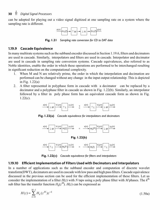
Another application of multirate signal processing is the conversion of an analog signal digitized at one sampling rate to another digital signal which is stored and retrieved at another sampling rate. For example CD quality voice is sampled, digitized and stored in the CD at the rate of 44.1 K samples/sec. When this signal is to be stored/read in/from a digital audio Tape (DAT), the samples have to be processed at the rate of 48 K samples/s. Hence for this application sampling rate conversion 44.1 /48 K samples is required. This is achieved by choosing an interpolator with a factor of 160 and a decimator with decimation factor of 147 as shown in Fig. 1.21. In Fig. 1.21, M=160 and N =147. Similar technique
Fig. 1.20 Linear fi ltering with2 polyphase fi lters
30 Digital Signal Processors
can be adopted for playing out a video signal digitized at one sampling rate on a system where the sampling rate is different.
Fig. 1.21 Sampling rate conversion for CD to DAT data
1.19.9 Cascade Equivalence
In many multirate systems such as the subband encoder discussed in Section 1.19.6, fi lters and decimators are used in cascade. Similarly, interpolators and fi lters are used in cascade. Interpolator and decimator are used in cascade in sampling rate conversion systems. Cascade equivalences, also referred to as Noble identities, enable the order in which these operations are performed to be interchanged resulting in signifi cant reduction on the computational complexity. 1. When M and N are relatively prime, the order in which the interpolation and decimation are
performed can be changed without any change in the input output relationship. This is depicted in Fig. 1.22(a)
2. A fi lter represented in polyphase form in cascade with a decimator can be replaced by a decimator and a polyphase fi lter in cascade as shown in Fig. 1.22(b). Similarly, an interpolator followed by a fi lter in poly phase form has an equivalent cascade form as shown in Fig. 1.22(c).
Fig. 1.22(a) Cascade equivalence for interpolators and decimators
Fig. 1.22(b)
Fig. 1.22(c) Cascade equivalence for fi lters and interpolators
1.19.10 Effi cient Implementation of Filters Used with Decimators and Interpolators
In a number of applications such as the subband encoder and computation of discrete wavelet transform(DWT), decimators are used in cascade with low pass and high pass fi lters. Cascade equivalence discussed in the previous section can be used for the effi cient implementation of these fi lters. Let us consider the implementation of a fi lter H(z) with N taps using a poly phase fi lter with M phases. The kth sub fi lter has the transfer function Hk(z
M). H(z) can be expressed as 1
0( ) ( )
MM k
kk
H z H z z-
-
== Â (1.50a)

An Overview of Digital Signal Processing and its Applications 31
1 2( ) (0) (1) (2)k k k kH z h h z h z- -= + + + � (1.50b)
( ) ( )kh n h Mn k= + (1.50c)Polyphase fi lter in cascade with the decimator can be realized using two schemes shown in Fig.
1.23(a). The second scheme is obtained by using the cascade equivalence discussed in the previous section. Let us assume that the sub fi lters have direct form I realization scheme. In the fi rst scheme, each of the sub fi lters receive a new input at an interval of Ts (sampling rate fs = 1/Ts) and each sub fi lter needs to perform one multiplication and (N/M) – 1 additions within this interval. In the second scheme, each of the sub fi lters receive a new input at an interval of MTs and each sub fi lter needs to perform one multiplication and (N/M) – 1 additions within this interval. Hence, scheme 2 requires multipliers and adders whose speeds are M times smaller. This not only reduces the cost but also the power dissipation.
Similarly, interpolators in cascade with low pass/high pass fi lters are used in synthesis section of sub band coders and in the computation of inverse DWT. The interpolator and the fi lter using poly phase form have two equivalent implementation schemes as shown in Fig. 1.23(b). Scheme 2 requires slower and cheaper hardware and hence is to be preferred.
Fig. 1.23(a) Effi cient implementation of decimator fi lter
Fig. 1.23(b) Effi cient implementation of interpolator fi lter

32 Digital Signal Processors
1.19.11 Realisation of Time Division Multiplexer, Frequency Division Multiplexer and Transmultiplexer Using Mutirate Signal Processing
Fig. 1.24(a) shows the block diagram of a time division multiplexer. This is used in short haul com-munication. In this case, each of the input is digitized using an A/D converter before multiplexing. Fig. 1.24(b) gives the block diagram of the demultiplexer for the multiplexed data. For long haul commu-nication, frequency division multiplexing is used. It may involve one or more analog exchanges. Fig. 1.25(a) shows the block diagram Frequency division multiplexer realized using interpolators and a bank of synthesis fi lters. It converts TDM signal into FDM signal. Fig. 1.25(b) shows the block diagram of Frequency division demultiplexer realized using decimators and a bank of analysis fi lters. It converts the FDM signal into TDM signal. The TDM-FDM-TDM converter is called as transmultiplexer. It takes digitized signal such as voice from M users and send them as FDM signal. y(n) denotes the FDM out-put. The D/A converter at the output of the FDM signal enables this signal to be processed by analog exchanges. The analog FDM signal originating from the analog exchange is digitized using the A/D before conversion to TDM signal.
Fig. 1.24(a) Block diagram of a time division multiplexer Fig. 1.24(b) Block diagram of the TDM demultiplexer
Fig. 1.25(a) Block diagram of TDM- FDM converter Fig.1.25(b) Block diagram of FDM- TDM converter
Let us consider the example of a transmultiplexer for M = 4, Fig. 1.26 shows the spectrum of four signals x0(n) – x3(n). Fig. 1.27 shows the spectrum at the output of the interpolators. By choosing the synthesis fi lter F0(z) – F3(z) to have equal bandwidth of p/2 and non overlapping passbands, the multiplexed output y(n) whose spectrum is given in Fig. 1.28 can be obtained. The output of the transmultiplexer xŸ0(n) – xŸ3(n) will be perfect reconstruction of x0(n) – x3(n) excepting for a delay by n0 samples if the analysis fi lters H0(z) – H3(z) and synthesis fi lters F0(z) – F3(z) satisfy the condition

An Overview of Digital Signal Processing and its Applications 33
Fk(z) G�(z) = dk� z–n0 k = 0,1..3, � = 0,1 ... 3 (1.51a)
where dk� is the kronecker delta.
x3(
)w
wp–p– ––
p2
––p2
x2(
)w
wp–p
– ––p2
––p2
0
0
x1(
)w
wp–p
– ––p2
0
x0(
)w
wp–p
– ––p2
––
––
p2
p2
0
Fig. 1.26 Spectrum of the input signals to be multiplexed
1.19.12 Implementation of Orthogonal Frequency Division Multiplexing (OFDM) System
A simplifi ed block diagram of an OFDM system is shown in Fig. 1.29. It uses M orthogonal carriers for transmitting M data streams. For this reason, it is called as discrete multitone transmission system.This differs from the conventional FDM in two aspects: 1. In the conventional FDM, the signal to be multiplexed originate from M different users. Each
user is allocated one channel or band of frequencies. In the case of OFDM, the data originating from a single user is split into M substreams, each substream data is sent over one of the M channels.
2. In the conventional FDM, M distinct carriers which are amplitude modulated (single sideband modulation) by the signal from M users need not be harmonically related. M carriers used in the case of OFDM are integral multiple of a fundamental frequency

34 Digital Signal Processors
X3¢( )w
X2¢( )w
X1¢( )w
0 p 2pp2—
3p2—
w
w
w
w
0 p 2pp2—
3p2—
0 p 2pp2—
3p2—
0 p 2pp2—
3p2—
X0¢( )w
Fig. 1.27 Spectrum at the output of the interpolators
0 p 2pp2—
3p2—
w
Y ( )w
Fig. 1.28 FDM output
To understand the operation of the OFDM, let us consider 3 orthogonal carrier signals shown in Fig.1.30. They can be expressed as
sk(t) = cos(kw0t) where k =1,2,3 By shifting these signals by 90° we can get
sk(t) = sin(kw0t)Using these two sets of signals, complex carrier signals can be obtained as follows:
sk(t) = cos(kw0t) + j sin(kw0t) = e+jkw0t (1.51b)
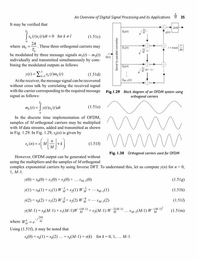
An Overview of Digital Signal Processing and its Applications 35
It may be verifi ed that
0
0
( ) ( ) 0 forT
k ls t s t dt k l= πÚ (1.51c)
where 00
2Tpw = . These three orthogonal carriers may
be modulated by three message signals m1(t) – m3(t) individually and transmitted simultaneously by com-bining the modulated outputs as follows
31( ) ( ) ( )k kky t s t m t== Â (1.51d)
At the receiver, the message signal can be recovered without cross talk by correlating the received signal with the carrier corresponding to the required message signal as follows:
0
0
( ) ( ) ( )T
k km t y t s t dt= Ú (1.51e)
In the discrete time implementation of OFDM, samples of M orthogonal carriers may be multiplied with M data streams, added and transmitted as shown in Fig. 1.29. In Fig. 1.29, sk(n) is given by
( )kns n s M kM
Ê ˆÍ ˙= +Í ˙Á ˜Ë ¯Î ˚ (1.51f)
However, OFDM output can be generated without using the multipliers and the samples of M orthogonal complex exponential carriers by using Inverse DFT. To understand this, let us compute y(n) for n = 0, 1, M–1.
y(0) = s0(0) + s1(0) + s2(0) + … sM–1(0) (1.51g)
y(1) = s0(1) + s1(1) W –1M + s2(1) W –2
M + � M–1(1) (1.51h)
y(2) = s0(2) + s1(2) W –2M + s2(2) W –4
M + � sM–1(2) (1.51l)
y(M–1) = s0(M–1) + s1(M–1)W –M(M–1) + s2(M–1) W –
M2(M–1) … sM–1(M-1) W –
M(M–1)2
(1.51m)
where 2 kjk M
MW ep-
=
Using (1.51f), it may be noted that
sk(0) = sk(1) = sk(2) … = sk(M–1) = s(k) for k = 0, 1, … M–1
Fig.1.29 Block diagram of an OFDM system using orthogonal carriers
Fig. 1.30 Orthogonal carriers used for OFDM

36 Digital Signal Processors
Using this (1.51g–1.51m) can be written in the matrix form as follows:
1 2 3 ( 1)
2 4 6 2
1
1 1 1 1 ... 1(0)1 ... (1)
(2) 1 ... ...
( )
MM M M M
M M M M
M
yW W W Wy
y W W W W
y
- - - - -
- - - -
-
È ˘Í ˙Í ˙Í ˙ =Í ˙Í ˙Í ˙Î ˚ 2
( 1)
( 1) 2( 1) 3( 1) ( 1)
(0)(1)(2)
... . .. ( 1)1 ...
M
M M M MM M M M
sss
s MW W W W
-
- - - - - - - -
È ˘ È ˘Í ˙ Í ˙Í ˙ Í ˙Í ˙ Í ˙Í ˙ Í ˙Í ˙ Í ˙Í ˙ Í ˙-Í ˙ Î ˚Î ˚
(1.51n)
From (1.51n), it may be noted that y(0) – y(M–1) can be obtained by fi nding the inverse DFT of the sequence s(0)–s(M–1). The IDFT can be computed effi ciently using the FFT algorithm.When the input to the IDFT block is real, the IDFT coeffi cients become complex valued. This requires two channels for transmitting the real and imaginary components. In order to overcome this limitation, the input to the IDFT block is formed as follows:
Let ak(t), bk(t) for k = 1,2, … M–1 be two real valued data streams sampled at a rate of FT that are to be transmitted. A new set of complex data stream, ak(n) of length N = 2M is formed as follows:
0 0,
[ ] [ ] 1 12
[ ]0 ,
2
[ ] [ ] 1 12
k k
k
N k N k
kNa n jb n k
n Nk
Na n jb n k N
a
- -
=ÏÔÔ + £ £ -ÔÔ= Ì =ÔÔÔ - + £ £ -ÔÓ
(1.51o)
Applying the inverse DFT to the above set of N sequences, we get the sequence ul(n). 1
0
1[ ] [ ] , 0,1,...., 1N
kk N
Ku n n W N
Na
--
== = -Â �
� � (1.51p)
N
N
N D/ALowpassfilter
z–1
z–1
a0( )n
a1( )n
aN–1( )n
N-p
oin
tID
FT
U n0( )
u n1( )
u nN–1( ) x ta( )
Fig. 1.31 Block diagram of DMT transmitter using the IDFT block.
The manner in which ak(n) is formed ensures that ul(n) is real valued. The N transform coeffi cients (ul(n)) may be converted to a serial stream using interpolators and delay elements and converted into

An Overview of Digital Signal Processing and its Applications 37
analog signal using a D/A converter and a fi lter. The resulting analog signal xa(t) is transmitted over the channel. Fig. 1.31 shows the block diagram of the DMT transmitter using the above processes.
Fig. 1.32 shows the block diagram of the DMT receiver. At the receiver, the received signal ya(t) is passed through an antialiasing fi lter and converted into digital data using a sample and hold circuit and an A/D converter. A sampling rate NFT is used for both A/D, D/A and S&H converters. The data stream is converted to parallel form using the decimator and delay elements. The resulting N parallel streams vk(n) are applied to the DFT block and the DFT coeffi cients bk(n) are generated using the equation:
1
0[ ] [ ] , 0,1,. . ., 1
Nk
k Nn n W k Nb u-
-
== = -Â �
��
(1.51q)
If we assume the frequency response of the channel to have fl at passband, A/D and D/A converters to be linear and assume the analog reconstruction and antialiasing fi lters to be ideal low pass fi lters, we can assume y[n] = x[n]. From the manner in which the interleaving and deinterleaving is performed in Fig. 1.31 and Fig. 1.32 respectively, the sequences at the receiver can be shown to be related to that of the transmitter as follows:
vk(n) = uk-1(n–1) k = 1,2, ... N–2 (1.51r)v0(n) = uN–1(n) (1.51s)bk(n) = ak–1(n–1) k = 1,2, ... N–2 (1.51t)b0(n) = aN–1(n) (1.51u)
1.19.13 Applications of DMT
Digital Subscriber Loop (DSL) Modems The frequency response of the twisted pair used for car-rying the signal from the telephone exchange to the subscriber premises is not fl at if a large frequency band is considered.
Figure 1.33 shows the magnitude of the Frequency response of a band limited channel. If a high speed data is to be directly transmitted over the channel, a complex equalizer is required for perfect reconstruction. However, if the datastream is split into a number of substreams and DMT is used for transmission, then frequency band occupied by each of the subcarriers and sidebands after modulation by each substream occupies only a fraction of the entire bandwidth. If the subchannels are of smaller bandwidth as shown in Fig. 1.32, the frequency response can be assumed to be fl at within this band. In this case, the equalizer required becomes merely a gain adjustment scheme for each of the substream. Hence, the attenuation of the channel for each of the substream data can be found by sending a test data. By providing suffi cient amplifi cation, imperfections in the
N
N
N
A/DLowpassfilter
z–1
z–1
b0( )n
bN–1( )n
N-p
oin
tID
FT
y n( ) v n0( )
v nN–1( )
x ta( )S H/
v n1( ) b1( )n
Fig. 1.32 Block diagram of the DMT receiver
Fig. 1.33 Frequency response of a band limited channel

38 Digital Signal Processors
channel can be compensated. Moreover, if the signal strength is low in some of the sub channels, data rate can be reduced in those sub channels and error control coding can be adopted to reduce the errors. DSL modems use DMT scheme. The data transmission rate required from an internet server to the client at customer premises is much higher compared to that required from the client to the server. For this reason, the modem used in the digital subscriber loop is called as asymmetric digital subscriber loop (ADSL) modem. The data transmitted from server to client is called as downstream data and the data rate is 24Mbps in ADSL2. The data transmitted in the reverse direction is called as upstream data and the data rate is 1.3 Mbps in ADSL2.
Modems for Wireless LANs The advantages of using MCM holds good for the wireless channel as well. In addition to this, it can also remove ambiguity due to multipath propagation. For example, if the data transmission rate is 50 Mbps, bit time is 20 ns. If the propagation delay between two paths is of the order of 20ns, at the receiver, both nth and (n+1)th bits will be received simultaneously through two paths and it may become diffi cult to demodulate the data. If the substream data rate is 1 Mbps, the difference in propagation delays will have negligible effect on the demodulation. The signal strength in the channel decreases with frequency and also with distance. In order to minimize the errors, error control coding may be used and in this case it is called as coded OFDM.
DISCRETE WAVELET TRANSFORM 1.20Our eyes and ears can resolve low frequency signals better than the high frequency signals. Hence, we require better frequency resolution at low frequencies. The high frequency signals are normally of shorter duration and hence we require better time resolution at high frequency. In order to analyze both high and low frequency components of a signal properly, we require multi resolution capability or ability to provide different resolutions at different frequency bands. STFT does not have the multi resolution capability.
The continuous wavelet transform and discrete wavelet transform have multiresolution property and are extensively used for the analysis and classifi cation of signals.
The continuous wavelet transform of a function f(t) is defi ned as
( ( ), , ) ( ) tWT f t s f t dts
tt y•
-•
-Ê ˆ= Á ˜Ë ¯Ú (1.52a)
where t
sty -Ê ˆ
Á ˜Ë ¯ is called as a small wave or mother wavelet. t and s are called as the translation and
scaling parameter. Examples of typical wavelets used for analysis are shown in Fig. 1.34. Since wavelet is of fi nite duration, the parameter t determines the time interval overwhich the mother wavelet is nonzero. The parameter s determines the width of the interval over which the wavelet is non zero. The discrete time version of CWT is called as the discrete wavelet transform. Every mother wavelet does not have a DWT representation. For a CWT to have a DWT, it should be realizable using a two channel fi lter bank as shown in Fig. 1.35 . Another equivalent condition for the existence of DWT is to test whether the scaling equation given by
( ) ( ) (2 )n
t g n t nf f= -Â (1.52b)
exists, where the actual wavelet is computed with

An Overview of Digital Signal Processing and its Applications 39
10.8
0.6
0.4
0.2
0
–0.2
–0.4
–0.6
–0.8
14 3 2 01 1 2 3 4
Morlet wavelet
0
.5
1
1.5
–0.5
–1
–15–8 –6 –4 –2 0 2 4 6 8
Meyer wavelet
1
0.8
0.6
0.4
0.2
0
–0.2
–0.4
–0.6
–0/8
–1–5 –4 –3 –2 –1 0 1 2 3 4 5
Mexican hat
1
0
–1
–1.0 –0.5 –0 0.5 1.0Harr wavelet
1.5
1
0.5
0
–0.5
–1
–1.5
10 0.5 1 1.5 2 2.5 3
Daubechies 4 tap wavelet
Scaling function
Wevlet function
Fig. 1.34 Some mother wavelets
( ) ( ) (2 )n
t h n t ny f= -Â (1.52c)
Here, g(n) is a low pass fi lter and h(n) is a high pass fi lter. In Fig.1.34a, the decimated outputs of low pass and high pass fi lters are denoted as l and g and are called as scaling coeffi cient and wavelet coeffi cient.
1.20.1 Discrete Wavelet Analysis of Signals Using Filter Banks
In discrete wavelet analysis, a signal is represented using a set of basis functions called as the wavelets. These basis functions are obtained by shifting and dilating(scaling) the mother wavelet sequence h(n). If a signal x(k) is represented using m basis functions given by
hi(2i+1 n – k) for ( 0 £ i £ m–1, –μ < k < μ )
the 1 dimensional discrete wavelet transform (DWT) is defi ned as
1( ) ( ) (2 ) for 0 2ii iy n x k h n k i m
•+
-•= - £ £ -Â (1.52d)
11 1( ) ( ) (2 ) for 1m
m my n x k h n k i m•
-- -
-•= - = -Â (1.52e)
yi(n) are called as the wavelet coeffi cients. The inverse discrete wavelet transform is computed by the expression
x n( )
H z( )
G z( )
2
2
g
l
Fig. 1.35 Filter bank for the computation of 1 D DWT

40 Digital Signal Processors
( ) ( )2 1 1( ) ( 2 ) ( 2 )1 10
m i mx n y k f n k y k f n ki i m mi k k
- • •+ -= - + -Â Â Â - -= = -• = -•
(1.52f)
where fi (n – 2i+1k) are designed such that (1.52f ) perfectly reconstructs the original signal x(n). It may be noted that the computation of the DWT and IDWT coeffi cients are similar to convolution operations. They can be calculated recursively as a series of convolutions and decimations using fi lter banks considered in section 1.19.6.
For e.g., let us consider the computation of the DWT for m = 4 using fi lter banks. The wavelet coeffi cients are given by
( )0 0( ) ( ) 2y n x k h n k•
-•= -Â (1.52g)
( ) ( ) ( )1 1 4y n x k h n k•
-•= -Â (1.52h)
( ) ( ) ( )2 2 8y n x k h n k•
-•= -Â (1.52i)
( ) ( ) ( )3 3 8y n x k h n k•
-•= -Â (1.52j)
They can be computed using the analysis fi lter banks with the decimators given in Fig.1.36.
x n( )
H0(z)
H1(z)
H2(z)
H3(z)
y n0( )
y n1( )
y n2( )
y n3( )
2
8
8
4
x n( )H0(z)
H0(z)
H0(z)
H1(z)
H1(z)
H1(z)
y n0( )
y n1( )
y n2( )
y n3( )
2 2
2
2
2
2
Fig. 1.37 Synthesis fi lter bank for Inverse DWT Fig. 1.38 Octave band fi lter bank for DWT
The signal x(n) can be reconstructed by computing the inverse DWT using the interpolators and synthesis fi lter bank as shown in Fig.1.37. Discrete wavelet transform processes M samples at a time and generates M transform coeffi cients. When M is chosen to be of the form M = 2m the wavelet coeffi cients can be computed using the tree structured fi lter bank shown in Fig. 1.38. The tree has m nodes or level at which a low pass fi lter and a high pass fi lter is used. As the tree is traversed from the root towards the child nodes, the cut off frequency of the low pass fi lter decreases. However, the tree structure for the computation of DWT differs from that given in Fig.1.18. In this case in the tree the branch corresponding to the output of the low pass fi lter alone is split into branches; the high pass output is not split further.
2
8
8
4
x n( )H0(z)
H1(z)
H2(z)
H3(z)
y n0( )
y n1( )
y n2( )
y n3( )
Fig. 1.36 Analysis fi lter banks for discrete wavelet transform

An Overview of Digital Signal Processing and its Applications 41
Such a special kind of pruned – tree fi lter bank is called as the octave band fi lter bank. The resulting tree structure for 3 level 1D DWT (i.e., m = 3) is shown in Fig.1.38.
1.20.2 DWT for Two Dimensional Signals
The wavelet theory can be extended for the analysis of 2 dimensional signals and can be used for the compression of 2D signals such as image data. Fig.1.39 shows the fi lter bank used for the computation of one level 2D DWT. In this fi gure, the image matrix is converted into a vector and the resulting input samples x(n) are passed through the 2 stages of analysis fi lters. In the fi rst stage it is passed through the low pass and high pass horizontal fi lters (h(n) and g(n)) and are sub sampled by two. In the second stage, the output of these two fi lters are processed by low pass and high pass vertical fi lters. Because of the decimation by a factor of 2 at the output of both horizontal and vertical fi lters, if an image matrix of size 512X512 is fed as input to the one level 2D DWT, all the four sub bands (LL1, LH1, HL1, HH1) contain 256X256 transform coeffi cients. In the 2 level 2D DWT, LL1 component alone is passed through horizontal and vertical fi lters. In the 3 Level DWT, LL2 component is passed through horizontal and vertical fi lters. The size of the various sub bands corresponding to 3 level DWT is shown in Fig.1.40. For image processing applications, wavelet transform is increasingly used. They have a number of advantages over the other transforms. One of the advantages is that a subset of the transform coeffi cients represents a coarse form of the image and can be displayed without computing the inverse transform. This has an attractive application in Progressive Image transmission (PIT) scheme used for Internet applications. It has proved its effi ciency in many other fi elds ranging from general-purpose multimedia to medical imaging. As a consequence, it is a part of the JPEG 2000 standard for still image coding.
2
2
2
2
2
2
h n[ ]
h n[ ]
h n[ ]
g n[ ]
g n[ ]
g n[ ]
x(n)
L1
L2
LL1
LH1
HL1
HH1
LL3 HL3
LH3 HH3
LH2 HH2
HL2
HL1
HH1LH1
Fig. 1.39 Block diagram of one level 2D DWT Fig. 1.40 Subbands corresponding to 3 level 2D DWT
1.20.3 Condition for Perfect Reconstruction of Signals Using 2 Channel Filter Banks
Two channel analysis and synthesis fi lters banks are cascaded in applications such as computation of wavelet transform and reconstruction of the signal from the wavelet coeffi cients. Such a fi lter bank along with decimator and interpolator is shown in Fig.1.41. The fi lters at the analysis section and synthesis section may be chosen to satisfy the QMF property. The z transform of the output sequence y(n) can be obtained from the z transform of the input sequence x(n) as follows:
Let v0[n] and v1[n] denote the outputs of the analysis fi lters. u0[n] and u1[n] denote the outputs of the analysis fi lters after decimation by 2. vŸ0[n] and vŸ1[n] denote the outputs of the interpolators. Hk(z) and Gk(z) denote the transfer function of the analysis and synthesis fi lters respectively (k takes the values 0 and 1 corresponding to the two fi lters in the fi lter bank). The z transform of the outputs of the analysis fi lter (Vk(z)) can be written as

42 Digital Signal Processors
Fig. 1.41 Two channel fi lter bank with decimator and interpolator
Vk(z) = Hk(z)X(z) (1.53)Using (1.47o) and (1.48) respectively, the outputs of the decimators (Uk(z)) and the z transforms of
the outputs of the interpolators (VŸ
k(z) can be written as.
{ } { }1 1( ) ( ) ( ) ( ) ( ) ( ) ( )2 2
k k k k kV z V z V z H z X z H z X zŸ È ˘= + - = + - -Í ˙Î ˚
(1.54a)
(VŸ
k(z) = Uk(z)2 (1.54b)
The z transform of the fi nal output (Y(z)) obtained by combining the outputs of the synthesis fi lter is given by
10 0 1( ) ( ) ( ) ( ) ( )Y z G z V z G z V zŸ Ÿ
= + (1.55)
{ } { }0 0 1 1 0 0 1 11( ) ( ) ( ) ( ) ( ) ( ) ( ) ( ) ( ) ( ) ( )2
Y z H z G z H z G z X z H z G z H z G z X z= + + - + - - (1.56)
The second term in (1.56) is the aliasing component due to sampling rate conversion. It can be made zero by properly choosing transfer function of the analysis and synthesis fi lter bank. One of the choices is
H1(z) = H0(–z)
G0(z) = H1 (–z) G1(z) = –H0 (–z)
1.20.4 Effi cient Implementation of 2 Channel Filter Banks
Two channel fi lter bank shown in Fig. 1.35 and Fig. 1.39 may be effi ciently implemented using poly phase structure with 2 phases and using cascade equivalence. A more effi cient implementation scheme for wavelet transform is proposed by Swelden [1998] and is referred to as the lifting scheme. This uses a polyphase structure for the analysis fi lter and uses a transformation which permits the use of integer wavelet and scaling coeffi cients instead of fl oating-point coeffi cients. The lifting scheme requires less hardware complexity and memory.
For obtaining the lifting scheme, fi rst express the low pass fi lter G(z) and high pass fi lter H(z) in polyphase form with two phases as follows:
G(z) = G0(z2) + z–1G1(z2) (1.57a)
H(z) = H0(z2) + z–1H1(z2) (1.57b)The l(z) and g (z), the transform of scaling coeffi cients and wavelet coeffi cients can be written as

An Overview of Digital Signal Processing and its Applications 43
l(z) = G0(z2)X0(z2) + z–1G1(z2)X1(z2) (1.57c)
g (z) = H0(z2) X0(z2) + z–1H1(z2) X1(z2) (1.57d)where X0(z2), X1(z2) denote the z transform of the even indexed and odd indexed input samples respectively. (1.57a) and (1.57b) can be written in the matrix form as follows
2 1 2 20 1 0
2 1 2 20 1 1
( ) ( ) ( )( )( ) ( ) ( ) ( )
G z z G z X zzz H z z H z X z
lg
-
-
È ˘ È ˘È ˘= Í ˙ Í ˙Í ˙
Í ˙ Í ˙Î ˚ Î ˚Î ˚ (1.57e)
2
02
1
( )( )
( )
X zP z
X z
È ˘= Í ˙
Í ˙Î ˚ (1.57f)
P(z) is called as the polyphase matrix. It is factored into the following form to obtain the lifting structure:
[ ]2 2
0 12 2
0 11
0( ) ( ) 1 ( ) 1 0( )
( ) 10 10 ( ) ( )
È ˘È ˘ È ˘ È ˘Í ˙= =Í ˙ Í ˙ Í ˙Í ˙Í ˙ Î ˚ Î ˚Î ˚ Î ˚’ i
ii
K
K
G z G z s zP z
t zH z H z (1.57g)
The resulting fi lter structure is shown in Fig.1.42. The advantage of this structure is that the low pass and high pass fi lter outputs are computed using a number of sub fi lters of smaller length. This can result in upto 50% reduction in the number of multiplications.
Fig. 1.42 Computation of 1 level 1D DWT using lifting scheme
ADAPTIVE FILTERS 1.21As mentioned in Section 1.3, inverse fi lters and equalizers are used in a numbers of applications. The impulse response coeffi cients of these fi lters may have to be varied with respect to time as the original degradation mechanism itself may vary w.r.t time. For example, the charactersitics of the channel through which the signal is transmitted and reaches the receiver may change with time. A fi lter in which the fi lter coeffi cients are adapted to ensure that the desired signal is obtained as faithfully as possible is called an adaptive fi lter. If d(n) is the desired signal and y(n) is the output of the fi lter, the error e(n) at the output of the fi lter at the nth sampling instant is given by
e(n) = d(n) – y(n) One of the methods used for choosing the fi lter coeffi cients of the adaptive fi lter is to choose the
coeffi cients so as to minimise the mean square error E[e2(n)]; e(n) is a random variable which can take any value between –2N–1 to 2N–1 where N is the no. of bits used for representing a no. in the fi lter. Knowing the probability distribution of d(n) and y( ) , the mean square error (MSE) can be computed. One of the popularly used technique for adaptive fi lter uses the FIR structure given in Fig. 1.43 and is called

44 Digital Signal Processors
as the Wiener fi lter. The fi lter coeffi cients are adapted so as to minimize the MSE. If h(i)
n denotes the nth fi lter coeffi cient at the ith iteration, then its value at the (i+1)th iteration h(i+1)
n is given by
h(i+1)n = h(i)
n + e(n)ax(n) (1.58)the value of a should be chosen to be in the range
0 < a £ [1/ (N E(x2(n))]where x(n) is the input to the adaptive fi lter and E(x2(n)) denotes the average input signal power. The algorithm used above for the adaptation is called as the least mean square algorithm (LMS).
In addition to the adative equalizers and inverse fi lters which may require adaptive fi lters, the adaptive fi lters are used in a number of applications. For example an application may require the ambient noise present to be cancelled in preference to the signal. This for example, could be used in an audio system used in an automobile. Since the background noise depends on the objects present, the noise generated would also change with time. The LMS algorithm can be used to adjust the fi lter coeffi cients to reduce the interference. The noise can be modelled as autoregressive or autoregressive moving average process. They are equivalent to outputs of FIR and IIR fi lters respectively.
IMAGE DATA COMPRESSION 1.22
1. 22.1 Discrete Cosine Transform and JPEG Standard
One of the popular methods used for compression of image data is using a combination of sample domain and transform domain techniques. An image may be considered to be consisting of a large number of picture elements called as pixels. The image intensity corresponding to each of these pixels is digitized and processed further for either storage or transmission to another point. The no. of pixels which constitutes an image depends on the image resolution used. One of the standards used is to assume the image to have 512 ¥ 512 pixels/ frame. On the other hand the VGA standard assumes a resolution of 640 ¥ 480 pixels/frame. Real time transmission of images requires 25 frames to be transmitted/sec. For monochrome images with a resolution of 512X512 this requires a transmission rate of about 50 Mbps assuming 8 bit accuracy/pixel. For colour images, the transmission rate becomes 150 Mbps. This calls for a large bandwidth and hence, the image data has to be compressed for transmitting it using a moderate BW. For compression of images two commonly used standards are the Joint Photographic Expert Group (JPEG) and Motion Picture Experts Group (MPEG). JPEG is used for still images and MPEG is used for moving images. They both make use of discrete cosine transform for image data compression.
An orthogonal transform is said to be effi cient if it is able to pack the energy in the signal in the form of a set of samples in the fi rst few transform coeffi cients. This is useful for image transmission as well as storage as only less no. of coeffi cients need to be considered compared to the original signal. For the image data which can be approximated by a fi rst order Markov process to a good accuracy, DCT is an effi cient transform. X(k), the kth transform coeffi cient of 1 Dimensional DCT of a sequence x(n) of length M is given by
Fig. 1.43 Adaptive FIR fi lter

An Overview of Digital Signal Processing and its Applications 45
[ ]1
0( ) ( ) ( )cos (2 1) /2
M
nX k a k x n n k Mp
-
== +Â (1.59a)
Similarly x(n), the nth data in the sampled sequence, can be expressed in terms of the DCT coeffi cients as follows:
1
0
1( ) ( ) ( )cos[(2 1) / 2 ]M
KX n a k X k n k M
Mp
-
== +Â (1.59b)
where a(k) is 1/÷2 if k = 0 and is 1 if k π 0The M point DCT and IDCT can be computed using 2M point DFT of a sequence y(n) obtained as
follows:
y(n) = x(n) for 0 £ n < M = x(2M – n – 1) for M £ n < 2M (1.59c)
Let the kth DFT coeffi cient of y(n) be Y(k). The DCT coeffi cient X(k) is given by
X(k) = a(k)Y(k) e –j (kp/2M) for 0 £ k < M (1.60) = 0 otherwiseThe M point IDCT of the transform coeffi cients X(k) may be obtained by computing the Inverse DFT
of the 2M DFT coeffi cients Y(k) given byY(k) = X(k) for 0 £ k < M = 0 for k = M (1.61) = – X(2M–1–k) for M+1 £ k < 2M
If y(n) denotes the inverse DFT coeffi cients of Y(k), then x(n) is obtained from y(n) as follows:
x(n) = y(n) for 0 ≤ n < M (1.62)Since DFT can be computed using FFT, the computational complexity for DCT and IDCT are of the
order of M log2 2M.Image data is normally an M¥N 2D array. This may be converted to an 1 D array and the 1 D DCT
may be computed for data compression. Alternately, X(k, l), the MN 2D DCT coeffi cients of the 2 D image data array x(m,n) may be computed using the 2D DCT equation given by
1 1
0 0
(2 1) (2 1)( , ) ( , ) ( , )cos cos2 2
M N
m n
m k n lX k l k l x m nM N
p pa- -
= =
+ += Â Â (1.63)
The 2D image data array elements x(m,n) can be obtained from the 2D DCT coeffi cients X(k, l) using the inverse DCT and are given by
1 1
0 0
(2 1) (2 1)( , ) ( , ) ( , )cos cos2 2
M N
K l
m k n lx m n X k l k lM N
p pa- -
= =
+ += Â Â (1.64)
where a(k, l) = 1/√2 if k = 0 and l = 0 (1.65) = 1 k π 0 and l π 0To reduce the computational and storage requirements, the MXN image data array is split into square
blocks of size L¥L where (L < N).

46 Digital Signal Processors
DCT for each of these square blocks may be computed either using the 2D DCT or using 1D DCT. This also permits the computation of DCT using a no. of processors simultaneously. DCT coeffi cients may be truncated to be zero when their value is below a threshold for data compression. For this purpose either threshold coding or zonal coding may be used. See Jain [1995 ]. for more details.
Further, the DCT coeffi cients matrix becomes almost like an upper triangular matrix with almost identical elements along the off diagonals. This property is used to achieve further data compression using run length encoding. In this scheme, a sequence of data which has identical value is encoded into two n bit numbers where the fi rst number denotes the frequency of repetition of the number and the second number denotes the actual value of the number.
Fig. 1.44 Block diagram of the JPEG coding scheme
Block diagram of the JPEG coding scheme is shown in Fig. 1.44. Let the image resolution be 640 ¥ 480 pixels. The function performed by each of the blocks is as follows:
Block Preparation The given colour image matrix of size 640 ¥ 480 is split into 3 matrices one into 4800 luminance (Y) matrices each of size 8 ¥ 8, and the remaining into two 1200 matrices each of size 8 ¥ 8. They are called as the in phase (I) and Quadrature (Q) matrices. The Red, Green, Blue (RGB) components are mapped into Y, I, Q components using the equation given in (1.66).
Y = 0.30R + 0.59G + 0.11B (1.66) I = 0.60R – 0.28G – 0.32B Q = 0.21R – 0.52G + 0.31BThis is done in order to achieve data compression. Our eye has poor resolution to colour (chrominance)
information compared the intensity (Y) information. Hence the full image matrix is mapped into Y matrix. However the I and Q matrices representing the chrominance information is obtained by reducing the image matrix size by a factor of 2 along the X and Y coordinates.
Discrete Cosine Transform and Quantization DCT is computed for each of the 8 ¥ 8 matrices corresponding to the Y, I and Q components. The DCT has very good energy compaction. Hence in the DCT coeffi cients of an 8 ¥ 8 matrix, only the elements corresponding to the left hand top corner has signifi cant values as shown in Fig. 1.45. The higher order coeffi cients along the rows and column cor-respond to high frequency components and they need to be reproduced with only less no. of levels. This is because our eye has a poor high frequency response. Different coeffi cients are allocated different no. of bits based on their importance. One such allocation scheme is shown in Fig. 1.46.
Using this allocation scheme, the image matrix coeffi cients are modifi ed as shown in Fig. 1.47. For coding this image either the zonal coding or the threshold coding can be employed. The number of bits required for transmission is reduced further by encoding only the difference in the amplitude corresponding to the DC component in the successive blocks along the vertical and horizontal direction. This corresponds to the top left corner element of the 8 ¥ 8 transform matrix. This is called as the differential quantization and is used only for the DC coeffi cients.

An Overview of Digital Signal Processing and its Applications 47
90 50 24 16 16 32 0
102 86 46 20 8 16 0 0
62 48 36 16 16 16 0 0
24 20 16 12 24 32 0 0
16 16 16 0 0 0 0 0
16 16 32 32 0 0 0 0
32 32 0 0 0 0 0 0
0 0 0 0 0 0 0 0
Fig. 1.45 DCT coeffi cients of a 8X8 matrix
8 8 7 6 5 4 3 2
8 8 7 6 5 4 3 2
7 7 7 6 5 4 3 2
6 6 6 6 5 4 3 2
5 5 5 5 5 4 3 2
4 4 4 4 4 4 3 2
3 3 3 3 3 3 3 2
2 2 2 2 2 2 3 2
Fig. 1.46 Quantization table for the DCT coeffi cients
160 90 25 6 2 1 1 0
102 86 23 5 1 1 0 0
31 24 18 4 2 1 0 0
6 5 4 3 3 2 0 0
2 2 2 0 0 0 0 0
1 1 2 2 0 0 0 0
1 1 0 0 0 0 0 0
0 0 0 0 0 0 0 0
Fig. 1.47 Quantized DCT coeffi cients
Runlength Encoding The quantized matrix is converted in to a linear vector using the zig zag pattern. This helps to combine the 0s using run length encoding explained above.
Source Coding The resulting vector is further compressed using Huff man coding which allocates more number of bits for those amplitudes whose probability of occurrence is less and vice versa.
1.22.2 JPEG 2000 Standard
The JPEG2000 standard for still image compression uses wavelet transform. JPEG2000 is targeted for a no. of applications such as Internet , facsimile, Printing , Scanning, Digital photography, Remote Sensing, Medical imaging, E-commerce and Digital libraries. JPEG2000 is aimed at providing the following features:

48 Digital Signal Processors
Low Bit-rate Performance It should give acceptable quality below 0.25 bpp. Remote sensing and networking require this feature. Provision for both Lossless and Lossy Compression
Progressive Transmission The standard allows progressive transmission which enables images to be reconstructed with increasing pixel accuracy and resolution depending upon the size of the fi le transmit-ted. Region of Interest Coding It can preferentially allocate more bits to the regions of interest (ROIs) as compared to the non-ROI ones. For example, the area corresponding to the face may be allocated more bits than the rest of the body of a picture of a person.
Comparison of the Performance of JPEG2000 and JPEG Compression Schemes
The codestream obtained after compression of an image with JPEG 2000 is scalable. It can be decoded in a number of ways: by truncating the codestream at any point, one may obtain a representation of the image at a lower resolution, or signal-to-noise ratio. By ordering the codestream in various ways, applications can achieve signifi cant performance increases. However, this is achieved at the cost of higher computational complexity.
At compression ratios less than 25:1 or so, the JPEG performs better numerically than the wavelet coders. At compression ratios above 30:1, JPEG performance rapidly deteriorates, while wavelet coders degrade gracefully well beyond ratios of 100:1.
The block diagram JPEG2000 encoder and decoder are shown in Fig. 1.48 and Fig. 1.49 respectively. A brief description of the various blocks of the encoder are as follows:
Fig. 1.48 Block diagram JPEG2000 encoder
Fig. 1.49 Block diagram JPEG2000 decoder
Tiling The input image is partioned into a number of non overlapping blocks if the image is large. Each of these blocks is called a tile. Tile size of 256 ¥ 256 or 512 ¥ 512 is chosen in order to simplify the VLSI implementation of the encoder. Smaller tiles create more boundary artifacts and degrade the compression effi ciency.
DC Level Shifting The pixels in the image are normally stored as unsigned integers. For mathemati-cal computations, it is necessary to convert them into two’s complement form. The purpose of the DC

An Overview of Digital Signal Processing and its Applications 49
level shifting is to ensure that the input image samples have a dynamic range that is approximately centred around zero.
Multi-component Transform This is effective in reducing the correlations amongst the multiple components in a multicomponent image. This increases the compression performance. For this purpose, images in the RGB color space are transformed to another color space, leading to three components that are handled separately. There are two possible choices:
Irreversible Color Transform (ICT) uses the well known YCBCR color space. It is called “irreversible” because it has to be implemented in fl oating or fi xed point and causes round-off errors.
Reversible Color Transform (RCT) uses a modifi ed YUV color space that does not introduce quantization errors, so it is fully reversible. Proper implementation of the RCT requires that numbers are rounded as specifi ed that cannot be expressed exactly in matrix form.
2D DWT
JPEG 2000 uses two types of wavelet transforms:Irreversible This is implemented using a 9/7 Daubechies fi lter, whose analysis and synthesis fi lter coeffi cients are shown in Table 1.3
It is said to be “irreversible” because it introduces quantization noise that depends on the precision of the decoder. Reversible It uses the biorthogonal 5/3 Daubechies fi lter whose analysis and synthesis fi lter coeffi -cients are shown in Table 1.4. It uses only integer coeffi cients, so the output does not require rounding (quantization) and so it does not introduce any quantization noise. It is used in lossless coding.
The wavelet transforms are implemented using either the lifting scheme or convolution.
Table 1.3 Daubechies 9/7 analysis and synthesis fi lter coeffi cients
Analysis Filter Coeffi cients i Low-pass fi lter g(i) High-pass fi lter h(i) 0 0.6029490182363579 1.115087052456994
1± –0.2668641184428723 0.5912717631142470 2± –0.07822326652898785 –0.057543526228499573± 0.01686411844287495 –0.091271763114249484± 0.02674875741080976
Synthesis Filter Coeffi cients i Low-pass fi lter g(i) High-pass fi lter h(i) 0 1.115087052456994 0.6029490182363579
1± 0.5912717631142470 -0.2668641184428723 2± -0.05754352622849957 -0.07822326652898785 3± -0.09127176311424948 0.01686411844287495 4± 0.02674875741080976

50 Digital Signal Processors
Table 1.4 Daubechies 5/3 analysis and synthesis fi lter coeffi cients
Analysis Filter Coefi cients Synthesis Filter Coeffi cientsi Low-pass fi lter g(i) High-pass fi lter h(i) Low-pass fi lter g(i) High-pass fi lter h(i)0 6/8 1 1 6/8
1± 2/8 –1/2 1/2 –2/8
Quantization After the wavelet transform, the coeffi cients are scalar-quantized to reduce the number of bits required to represent them, at the expense of a loss of quality.
Entropy Coding A two step coding scheme (Tier 1 and Tier 2 coding) is adapted in JEPEG2000. In Tier 1 coding, Embedded block coding with optimized truncation (EBCOT) algorithm is used for com-pressing the quantized transform coeffi cients. Each sub band LL,LH,HL,HH is partitioned into small code blocks of size 32 ¥ 32 or 64 ¥ 64 . The EBCOT algorithm generates a highly scalable bit stream for each code block Bi. The bit stream associated with Bi may be independently truncated to a predeter-mined lengths depending upon the specifi ed distortion. Next a post compression rate distortion step is used to truncate the bit stream of each code block optimally so as to minimize the distortion subject to the bit rate contraint. Tier 2 coding is used to effi ciently represent the layer and block summary informa-tion for each code block.
LINEAR PREDICTIVE CODER AND SPEECH COMPRESSION 1.23Another application of digital signal processing is the data compression of the speech signal using the linear predictive coder. For this purpose the human vocal tract is modelled as a linear time varying fi lter. The voiced sounds(for example vowels) are produced by exciting this fi lter with quasi periodic impulses. These impulses are called quasi periodic as periods of the impulses are not exactly equal and the amplitude of the impulses are not exactly equal. The unvoiced sounds (for example S, SH) are produced by exciting the above fi lter with white noise. The time varying fi lter is normally approximated by a linear time invariant fi lter over short time intervals. One of the common models used for the vocal tract is the linear predictive coder which is a LTI fi lter over a short term interval where the output at the nth sample y(n) is predicted based on the past p samples and is given by
y(n) = a1y(n–1) + a2y(n–2) + � apy(n–p) + u(n) The error u(n) in turn may be obtained by exciting another linear LTI fi lter fed with another exciting
signal. In the European standard for cellular telephone GSM 6.10, the output rate of the speech coder used is 13 kbps and the input to the coder is voice signal sampled at the rate of 8 Kilo samples with 13 bits/samples. Hence the compression factor is 8. To achieve this, samples corresponding to every 20 msec are used to compute the LPC model parameters and the model parameters corresponding to excitation signal including the LTI fi lter used if any for generating the excitation. Additional details on estimating the LPC model parameters may be obtained from Rabiner and Juang [1993].

An Overview of Digital Signal Processing and its Applications 51
Review Questions 1.1 Find the output y(n) of a linear shift invariant system
with unit sample (impulse) response h(n) given by h(0) =
3, h(1) = 2, h(2) = 1 and h(n) = 0 for all other value of n if it
is fed with an input x(n) which is non zero for only for n =
0 and 1. x(0) = 2 and x(1) =1.
1.2 Show that the output y(n) of a causal linear time
invariant discrete time system for the input x(n) given by
x(n) = ejwn is y(n) = x(n) H(ejw) where H(z) is the system
(transfer) function of the LTI system.
1.3 Find the frequency response of the LSI causal
system given by y(n) = x(n) + a y(n–1) for a < 1 and sketch
the magnitude and the phase response of this system.
Find also its impulse response. Show that the phase
response of this system denoted as –H(ejw) is given by
–H(ejw) = w – tan–1(sin w / (a – cos w))
1.4 Find the frequency response of the LSI causal
system given by y(n) = x(n) + a y(n–2) for a < 1. Find also
its impulse response.
1.5 The magnitude of the frequency response of the
LSI causal system given by y(n) = x(n) – ax(n–1) + by
(n–1) is independent of frequency and a π b. Find the
relationship between a and b. Such a system is called as
an all pass system.
[Hint: Assume the magnitude of the numerator of the
frequency response to be k times the magnitude of the
denominator.]
1.6 Determine the impulse response coeffi cients of a
digital low pass fi lter with [H(ej2pf Ts) = 1 for f < fc and is 0
for fc < f < fs/2].
where fs = 1/ Ts is the sampling rate of the digital fi lter.
1.7 Determine the impulse response coeffi cients of a
digital fi lter with H(ej2pfTs) given in Fig. 1.
-350 -250 -50 50 250 350 550 650
f �
… 1 …
H ej fTs( 2 )� �
Fig. 1 Frequency response of the fi lter
1.8 Determine the impulse response coeffi cients of a
digital low pass fi lter with [H(ejw) = 1 for w < wc and is 0
for wc < w < p1.9 Determine the impulse response coeffi cients of a
digital fi lter with H(ejw) given in Fig. 2
… 1 …
������������������������������������������������������������������������������� ��
H e( )j �
Fig. 2 Frequency response of the fi lter
1.10 Sketch the frequency spectrum of f(t) = sin 2p(1250)
t. Determine the minimum sampling rate required to
reconstruct the signal from its samples. What should be
the cut off frequency of the reconstruction (smoothing)
fi lter? If the signal is sampled is at the rate of 2000
samples/s what would be the output of the smoothing
fi lter .
1.11 Sketch the frequency spectrum of
f(t) = sin 2p(1000)t + sin 2p(1250)t
Determine the minimum sampling rate required to
reconstruct the signal from its samples. What should be
the cut off frequencies of the reconstruction (smoothing)
fi lter? If the signal is sampled is at the rate of 2000
samples/s what would be the output of the smoothing
fi lter .
1.12 Let f(t) be sin2p(1000)t + sin2p(1250)t and y(t) =
[f(t)]2. Determine the minimum sampling rate required
to reconstruct y(t) from its samples. What should be the
cut off frequencies of the reconstruction (smoothing)
fi lter?
1.13 A continuous time signal is to be fi ltered to remove
frequency components in the range 10 kHz < f < 25 kHz.
The maximum frequency component present in the
signal is 50 kHz. If the signal is sampled at the Nyquist
rate what range of digital frequencies should be rejected
by the fi lter. Sketch the magnitude characteristics of the
ideal digital fi lter required for this purpose.
1.14 Find the impulse response of a system whose
system function is given by
- -=- +1 1
2( )(1 0.5 )(1 0.5 )
X zz z
1.15 Find the impulse response of a system whose
system function is given by
-
- --
=- -
2
1 1(3 )( )
(1 0.25 )(1 0.75 )zX z
z z

52 Digital Signal Processors
1.16 The impulse response of a discrete time system is
given by h(n) = a –n for 0 £ n £ 15 and 0 otherwise. Find
the system function of this fi lter.
1.17 The impulse response of a discrete time system is
given by h(n) = [ 1, 0.2, 0.04, 0.008, 0.0016, 0, 0, 0, …].
Find the system function of this fi lter.
1.18 For a sampling rate of 10KSPS and cutoff frequency
of 1 kHz, a low pass fi lter requires 18 taps. Under what
condition will the above fi lter work as a low pass fi lter
with cut off frequency of 100 kHz? Using the same idea,
the above fi lter was proposed to be used as a low pass
fi lter with cut off frequency of 10 MHz. However the
fi lter was found to be not satisfactory. What could be the
reason? (Hint: critical path delay)
1.19 Sketch the frequency response of QMF. How are
the impulse response of the two fi lters related?
1.20 The impulse response of a low pass fi lter is given
by the sequence { 0.9, 0.6, 0.3, 0.1, 0.03, 0.008}. If a high
pass fi lter is implemented as the QMF, fi nd its impulse
response.
1.21 (a) Find the system function of the following LTI
causal systems
(i) y1(n) = x1(n) + 0.25 x1(n–1) + 0.5 y1(n–1)
(ii) y2(n) = x2(n) + 0.5 x2(n–1) + 0.75 y2(n–1)
(b) If x2(n) = y1(n), fi nd the system function of the LTI
system whose input is x1(n) and the output is y2(n)
(c) If x1(n) = y2(n), fi nd the system function of the LTI
system whose input is x2(n) and the output is y1(n)
(d) If the systems given in (a) are cascaded, fi nd the
system function of an equivalent LTI system.
(e) If the systems given in (a) are connected in parallel,
fi nd the system function of an equivalent system.
1.22 Find the 3 point DFT of the sequence given by
x(n) = 1 for n = 0,1,2
1.23 Find the 8 point DFT of the sequence given by x(n)
= 1 for n = 0,1,2 and x(n) = 0 for n = 3, 4, … 7.
1.24 Find the 8 point DFT of the infi nite sequence
given by a(n) = (0.5)n for n = 0, 1, 2, ….
1.25 Find the 16 point DFT of the infi nite sequence
given by h(n) = (0.25)n for n = 0, 1, 2, ….
1.26 Show that the computation of the DFT of a N point
sequence is equivalent to a multiplication of matrix by a
vector. What is the (m,n)th element of this matrix.
1.27 It is required to design a low pass digital fi lter with
cut off frequency of 0.5p.
(a). If the sampling period is 1 sec, what should be the
cut off frequency of the corresponding analog fi lter if
the digital fi lter is designed using (i) impulse invariant
technique, and (ii) bilinear transform method.
(b). If the sampling period is 0.1 msec, what should be
the cut off frequency of the corresponding analog fi lter
if the digital fi lter is designed using (i) impulse invariant
technique (ii) bilinear transform method.
1.28 It is required to design a low pass digital fi lter
with cut off frequency of 0.5π. If the sampling period is
0.01 msec, what should be the cut off frequency of the
corresponding analog fi lter if the digital fi lter is designed
using (i) impulse invariant technique (ii) Bilinear
transform method.
1.29 Determine the impulse response coeffi cients of a
digital fi lter whose frequency response is given by
H(ejw) = 0 for |w| < .85p and is 1 for .85p < |w| < p1.30 (a) Obtain the impulse response of the analog
fi lter whose transfer function is given by
=-1( )0.5
H ss
(b) If the sampling rate used is 1/T what is the impulse
response of the equivalent digital fi lter obtained using
the impulse invariant method.
(c) What is the transfer function of the equivalent digital
IIR fi lter?
1.31 The transfer function of an analog fi lter is given by
=-1( )H s
s a
(a) What is the transfer function of the equivalent digital
IIR fi lter if bilinear transform is used to convert the
analog fi lter to the equivalent digital fi lter? Assume the
sampling rate to be 1/T.
(b) What is the impulse response of the equivalent digital
IIR fi lter?
1.32 Obtain the impulse response of the analog fi lter
whose transfer function is given by
=-
1( )0.75
H ss
If the sampling rate used is 10000 samples/sec what
is the impulse response of the equivalent digital fi lter
obtained using the impulse invariant method.
1.33 Determine the impulse response coeffi cients of a
digital FIR fi lter whose frequency response is given by
H(ejw) = 0 for |w| < .75p and is 1 for .75p < |w| < pusing a fi lter of order 8 and windowing using Black man
window given by
An Overview of Digital Signal Processing and its Applications 53
w(n) = 0.42– 0.5 cos (2pn/N–1) + 0.08cos(4pn/N–1) for
0 £ n £ N–1 = 0 otherwise.
1.34 A digital FIR fi lter of order 8 is to be designed
using the frequency sampling method. The frequency
response of the fi lter is given by
H(ejw) = 1 for |w| < .3p
= 0 for .3p < | w | < pDetermine the impulse response coeffi cients.
1.35 Show that the frequency response function
H(ejw) of a linear phase fi lter with M (odd) taps and with
impulse response h(n), n = 0, ... N–1 symmetrical about
(N–1)/2 is given by
w w w-
- -
== Â
( 1)/2( 1)/2
0( ) ( )cos
Nj j N
nH e e a n n
where a(0) = h[(N–1)/2] and a(n) = 2h[(N–1)/2 – n] for n
= 1,.. (N–1)/2
1.36 Show that the frequency response function H(ejw)
of a linear phase fi lter with M (even) taps and with
impulse response h(n), n = 0, ... N–1 symmetrical about
(N–1)/2 is given by
w w w- -
== -È ˘Î ˚Â
/2( 1/2)
1( ) ( )cos ( 1/ 2)
Nj j N
nH e e b n n
where b(n) = 2h[N/2 – n] for n =1, ... N/2
1.37 Show that the frequency response function
H(ejw) of a linear phase fi lter with M (odd) taps and with
impulse response h(n), n = 0, ... N–1 anti symmetrical
about (N–1)/2 is given by
w w p w-
- -
== Â
( 1)/2( 1)/2 /2
1( ) ( )sin( )
Nj j N j
nH e e e c n n
where c(n) = 2h[(N–1)/2 – n] for n = 1, ... (N–1)/2 and
h[(N–1)/2] = 0
1.38 Show that the frequency response function H(ejw)
of a linear phase fi lter with M (even) taps and with
impulse response h(n), n = 0, ... N–1 symmetrical about
(N–1)/2 is given by
w w p w- -
== -È ˘Î ˚Â
/2( 1)/2 /2
1( ) ( )sin ( 1/ 2
Nj j N j
nH e e e d n n
where b(n) = 2h[N/2 – n] for n =1,... N/2
1.39 Realize the system given by the transfer function
X(z) = a0 + a1 z –1 + a2z –2 + a3z –3 + a4z –4
in direct form I and direct form II.
1.40 Realize the system given by the transfer function
- - - -
- - - -+ + + +
=+ + + +
1 2 3 40 1 2 3 4
1 2 3 41 2 3 4
( )1
a a z a z a z a zH z
b z b z b z b z
in (a) direct form I (b) the transpose of direct form I (c)
canonic form
1.41 State and explain the three cascade equivalence
relations for the multirate DSP systems using block
diagrams.
1.42 With a diagram, explain how a poly phase fi lter
with three phases followed by decimator by a factor
of three can be effi ciently implemented using noble
identity. Compare the computational complexity with
the direct implementation approach.
1.43 Show how the computational complexity of an
FIR fi lter of order 21 can be reduced by using 3 polyphase
fi lters.
1.44 Find the output of the systems consisting of (i)
a decimator by 3 followed by a interpolator by 3 (ii) an
interpolator by 3 followed by a decimator by 3. If the
sequence 0, 1,2,3,4,5, …. is fed to both of the systems,
what will be the output of both of the systems?
1.45 Draw the block diagram of a sub band encoder for
speech signal. Explain how it can be implemented using
fi lter bank.
1.46 A multirate system is used to convert the sampling
rate from 32 to 48 KSPs. Show how this system can be
effi ciently implemented using noble identity.
1.47 Derive the condition for the perfect reconstruction
of 2 channel fi lter bank.
1.48 If transfer function of the high pass fi lter is
½(1– z–1), fi nd the T.F. of other fi lters at analysis and
synthesis sides for perfect reconstruction of a 2 channel
fi lter bank.
1.49 A low pass signal bandlimited to ±p/4 radians is
decimated by a factor of 4. Sketch the magnitude of the
frequency response at the output of the decimator.
1.50 Derive the z transform of the output of decimator
by a factor of M.
1.51 A 64 tap fi lter followed by decimation by 4 is
effi ciently implemented using poly phase scheme and
noble identity. The fi lters use multipliers and adders with
computation time of 8ns, 2ns. Compare the maximum
sampling rates of the original fi lter and the one using the
polyphase structure and noble identity. Assume Direct
Form I realization.
1.52 A low pass signal bandlimited to ±p/3 radians is
decimated by a factor of M. What is the maximum value
of M for which the aliasing does not occur. Sketch the
magnitude of the frequency response at the output of
the decimator corresponding to this M.

54 Digital Signal Processors
1.53 An interpolator by 4 followed by 128 tap fi lter is
effi ciently implemented using poly phase scheme and
noble identity. The fi lters use multipliers and adders with
computation time of 8ns, 2ns. Compare the maximum
sampling rates of the original fi lter and the one using the
polyphase structure and noble identity. Assume Direct
Form II realization.
1.54 Write the equation for the computation of short
time Fourier transform (STFT). How is its frequency
spectrum plotted? What are the limitations of STFT?
1.55 Given STFT, how is the original function f(n)
obtained?
1.56 What is meant by spectrogram? Give an example
plot.
1.57 What is the limitation of STFT? How does the
frequency resolution and time resolution vary with
window size?
1.58 Explain how STFT can be found using DFT/FFT.
1.59 What is the relationship between R and N of STFT?
(N > R) What do R and N denote?
1.60 The down stream data corresponding to ADSL
modem is split into no. of sub streams (e.g., using serial to
parallel converter) and each substream data modulates a
separate carrier. How is this scheme superior compared
to the case where the entire data stream modulates a
single carrier?
1.61 Why is multicarrier modulation scheme preferred
for wireless LAN?
1.62 Explain how the DFT techniques can be used for
transmission of discrete multi tone modulated signals.
1.63 802.11a WLAN systems employ a 64 point
transform with 52 of the subcarriers actually used for
Carrying user data from 16-QAM alphabet. 16 symbol
duration is used as guard time between adjacent block
of data.The symbol rate used is 20 Msymbols/sec What
is the bit rate corresponding to user data if (i) no error
correction code is used (ii) A convolution code with
coding effi ciency of 0.75 is used?
1.64 State the three differences between conventional
FDM scheme and OFDM.
1.65 What is meant by (i) coded OFDM (ii) Multirate
OFDM? What are their applications?
1.66 Draw the block diagram of OFDM transmitter and
OFDM receiver
1.67 State the relationship between the sequence at
the output of IFFT block and input of FFT block used with
the OFDM transmitter and receiver.
1.68 How is the input to the IFFT block formed from
the input data stream?
1.69 Write the equation for continuous time wavelet
transform. What is the condition to be satisfi ed for a
mother wavelet to have DWT?
1.70 What are the two advantages of DWT over DCT
for image Data compression
1.71 State two differences between basis functions
used for wavelet transform and Fourier series expan-
sion.
1.72 Draw the block diagram of 3 level ID DWT. Explain
how a single LPF & HPF may be used at all levels.
1.73 State the Heisenberg’s uncertainty principle w.r.t.
time & freq. resolution. Which function meets the bound?
1.74 Sketch the waveforms of any three wavelets.
1.75 Show that the computation of wavelet transform
is equivalent to analyzing a function using window
functions of varying durations.
1.76 Explain why different mother wavelets are used
for wavelet transform unlike the fourier series/FT?
1.77 Write the equation for continuous time wavelet
transform.
1.78 Does DWT exist corresponding to every CWT?
1.79 Explain how scaling function is obtained from
mother wavelet?
1.80 Explain how scaling function and wavelet function
at one level is related to scaling function at another
level
1.81 Draw the block diagram of 1 level 2D DWT.
Qualitatively explain how 2D DWT of an image of size
512 x 512 is computed. What is the size of each of the
transform coeff. matrices?
1.82 What are the two advantages of DWT over DCT
for image Data compression?
1.83 Show how a three level ID DWT consisting of 4
subband outputs can be obtained using a fi lter bank
consisting of 4 fi lters (Use Noble Identity). In the fi lters
used which parameter is the same for all the fi lters?
1.84 Write the polyphase matrix for the fi lter bank with
2 fi lters.
1.85 Explain the lifting scheme for the computation of
1 D DWT.
1.86 What is meant by (i) lifting (ii) dual lifting blocks?
1.87 What are the two steps which are repeatedly
carried out to derive the lifting structure? What are the
two advantages of lifting scheme over the conventional
scheme?
An Overview of Digital Signal Processing and its Applications 55
1.88 Show how Discrete cosine Transform (DCT) of
an 8 point sequence can be computed using a 2N point
FFT.
1.89 Show how the DCT coeffi cients of an eight point
sequence can be computed using a bank of fi lters.
Self Test Questions 1.1 y(n) denotes the output of a linear shift invariant
system with unit sample (impulse) response h(n) given
by h(0) = 3, h(1) = 2, h(2) = 1 and h(3) = 0.5. h(n) = 0 for
all other value of n. This system is fed with an input x(n)
which is non zero for only for n = 0, 1 and 2 with x(0) =
2, x(1) = 1 x(2) = 0.5. The minimum value of n (n > 0) for
which y(n) = 0 is
(a) 8 (b) 7 (c) 6 (d) 5
1.2 Which of the following systems are causal?
(a) y(n) = x(n) + 0.25 x(n–1) + 0.5 x(n–2)
(b) y(n) = x(n) + 0.25 x(n–3) + 0.75 y(n–1)
(c) y(n) = x(n) + 0.5 x(n–1) + 0.5 y(n–1) + 0.8 y(n–2)
(d) y(n) = x(n+1) – 0.5 x(n–1) + 0.8 x(n–1)
1.3 The minimum sampling rate required to reconstruct
the signal f(t) = sin 2pf(1000)t from its samples is ———
Hz.
(a) 500 (b) 1000
(c) 2000 (d) none of the above
1.4 The cut off frequency of the reconstruction
(smoothing) fi lter for a signal sampled at a frequency of
fs is ———.
(a) fs/2 (b) fs
(c) 2fs (d) fm i.e. the signal max. frequency
1.5 The signal f(t) = sin 2pf(1000)t is sampled is at the
rate of 1800 samples/sec. The frequency of the signal at
the output of the smoothing fi lter is ——— Hz.
(a) 1000 (b) 900 (c) 1100 (d) 800
1.6 Speech is digitized using a sampling rate of 8 kHz.
An antialiasing fi lter with cut off frequency of 3.4 kHz is
preceded by the sampler. The loss of the speech signals
in the frequency range 3.4–20 kHz due to antialiasing
fi lter introduces a degradation in the signal quality. On
the otherhand sampling without the antialiasing fi lter
also introduces degradation in the signal quality. Which
of the following statements are true.
(a) Degradation with antialiasing fi lter is less
(b) Degradation without antialiasing fi lter is less
(c) Degradation with or without the fi lter is the same.
1.7 The no. of stages of FFT computations required for
the computation of the DFT of a 512 point sequence is
———
(a) 9 (b) 8 (c) 7 (d) 6
1.8 At the 5th stage of FFT computation of a 512 point
FFT, the no. of distinct twiddle factors used is 2———.
(a) 2 (b) 3 (c) 4 (d) 5
1.9 Which of the the following properties are true for
an IIR fi lter designed using bilinear transform method.
(a) Requires the use of antialiasing fi lter
(b) Requires prewarping the fi lter cutoff frequencies
(c) Not suited for the design of high pass fi lters
(d) Results in unique mapping from analog to digital
frequencies.
1.10 Which of the the following properties are true for
an IIR fi lter designed using impulse invariant technique
.
(a) Requires the use of antialiasing fi lter
(b) Requires prewarping the fi lter cutoff frequencies
(c) Not suited for the design of high pass fi lters
(d) Results in unique mapping from analog to digital
frequencies.
1.11 Which of the following properties are true for the
linear phase FIR fi lter with even no. of coeffi cients and
symmetric impulse response.
(a) not suited for high pass fi lter but has real magnitude
response
(b) suited for high pass fi lter and has real magnitude
response
(c) has imaginary magnitude response
(d) suited for differentiators and hilbert transformers
1.12 Which of the following properties are true for the
linear phase FIR fi lter with odd no. of coeffi cients and
symmetric impulse response.
(a) not suited for high pass fi lter but has real magnitude
response
(b) suited for high pass fi lter and has real magnitude
response
(c) has imaginary magnitude response
(d) suited for differentiators and hilbert transformers
1.13 Which of the following characteristics are true for
a half band fi lter
(a) In a fi lter with M taps, the value of the coeffi cients of
the odd taps is zero.
(b) The frequency response of the fi lter is antisymmetric
w.r.t to the frequency fs/4 where fs is the sampling
frequency.

56 Digital Signal Processors
(c) The ripple in the pass band is equal to that in the stop
band.
(d) These fi lters are used in multirate systems
Table 1 Impulse response coeffi cients of 4 fi lters
Filter no
h(0) h(1) h(2) h(3) h(4) h(5) h(6)
I 2 6 7 6 2 0 0II 2 5 8 –5 –2 0 0III 2 3 4 4 3 2 0IV 2 0 3 0 2 0 0
1.14 Among the fi lters given in Table 1, the fi lter which
has imaginary magnitude response and is suited for
differentiators and hilbert transformers is
(a) I (b) II (c) III (d) IV
1.15 Among the fi lters given in Table 1, the fi lter which
is not suited for high pass fi lter but has real magnitude
response is
(a) I (b) II (c) III (d) IV
1.16 Among the fi lters given in Table 1, the fi lter which
is suited for high pass fi lter and has real magnitude
response
(a) I (b) II (c) III (d) IV
1.17 Among the fi lters given in Table 1, the fi lter
whose frequency response is antisymmetric w.r.t to the
frequency fs/4 is.
(a) I (b) II (c) III (d) IV
1.18 The no. of multiplications required for performing
the convolution of two sequences with identical length
8 using the direct method is
(a) 256 (b) 120 (c) 128 (d) 64
1.19 The no. of multiplications required for performing
the convolution of two sequences with identical length
8 using the indirect method using FFT is
(a) 256 (b) 120 (c) 192 (d) 185
1.20 A multirate system is required for converting the
sampling rate from 48 K samples to 42.1 K samples, the
interpolation factor, decimation factor to be used is
(a) 147, 160 (b) 160,147 (c) 480, 421 (d) 421,480
1.21 The z transform of the input to a decimator by
factor 4 is 1+ z–1 + z–2 + –3. The z transform at the output
is ———.