analytical thermal placement for vlsi lifetime improvement and minimum performance variation andrew...
Post on 21-Dec-2015
221 views
TRANSCRIPT

Analytical Thermal Placementfor VLSI Lifetime Improvement and
Minimum Performance Variation
Analytical Thermal Placementfor VLSI Lifetime Improvement and
Minimum Performance Variation
Andrew B. Kahng†, Sung-Mo Kang‡, Wei Li‡, Bao Liu†
†UC San Diego ‡UC Santa Cruz

OutlineOutline
Background
Modeling and Theoretical Results
Analytical Thermal Placement
Experiment
Summary

VLSI On-Chip Temperature ScalingVLSI On-Chip Temperature Scaling
40048008
80808085
8086
286386
486Pentium® proc
P6
1
10
100
1000
10000
1970 1980 1990 2000 2010
Year
Po
wer
Den
sity
(W
/cm
2)
Hot Plate
RocketNozzle
NuclearReactor
Courtesy, Intel

Temperature Scaling: Why and HowTemperature Scaling: Why and How
Scaling has led to temperature rise in VLSI Higher integration
Higher clock frequency
Leakage power
Cooling techniques are stagnant Air ventilation
Liquid cooling
Low power design Power gating, clock gating, dynamic scheduling
Placement

Chip Packaging StructuresChip Packaging Structures
Heat dissipation through bulk silicon in wire bond packaging
Devices and interconnects closer to heat sinks in flip chip packaging

Electrical analogue: RC Circuit
Thermal conductance G
Heat capacity C
From Boltzmann’s Equation
p ( r ) power density
g ( r ) thermal conductivity
Heat Dissipation Equations Heat Dissipation Equations
CT GT P
( , )[ ( , ) ( , )] ( , )p
T r trc g r t T r t p r t
t
2 T r p rg r( ) ( )
( )
Poission’s Equation
Purely Resistive Network
GT P
Dynamic Static

Thermal Effects on PerformanceThermal Effects on Performance Higher temperature
Superlinear decrease of carrier mobility
Linear decrease of transistor threshold voltage
Increase or decrease of transistor output current depending on transistor threshold voltage, supply voltage, etc.
Increase of interconnect resistance
m m( ) ( )( )T TrTT
k
r
s
V T V T k T TT T r r( ) ( ) ( ) 4

Circuit lifetime Tf decreases superlinearly with rising temperature
Hot carriers
Oxide breakdown
Electromigration
where J current density
Q activation energy (1.0eV for copper)
k Boltzmann constant
T temperature
D given by device structure
Thermal Effects on Circuit LifetimeThermal Effects on Circuit Lifetime
J t d t DekT
T Q
kTf
( )
0

Previous Thermal PlacersPrevious Thermal Placers Objective:
Total on-chip temperature1
Maximum on-chip temperature23
Method: Simulated annealing34
Min-cut bi-partition1
Thermal simulation Compute thermal resistance matrix at each iteration134
1. Chao and Wong, Thermal placement for high performance multichip modules, ICCD, 1995
2. Chu and Wong, A matrix synthesis approach to thermal placement, ISPD, 1997
3. Cong, Wei, and Zhang, A thermal-driven floorplanning algorithm for 3D IC, ICCD, 2004.
4. Tsai and Kang, Cell-level placement on improving substrate thermal distribution, IEEE Trans. CAD, 2000
OutlineOutline
Background
Modeling and Theoretical Results
Analytical Thermal Placement
Experiment
Summary

Thermal ModelingThermal Modeling
FDM (Finite Difference Method)
MOR (Model Order Reduction)
Heat source
Boundary thermal resistor
GT P
2 T r p rg r( ) ( )
( )
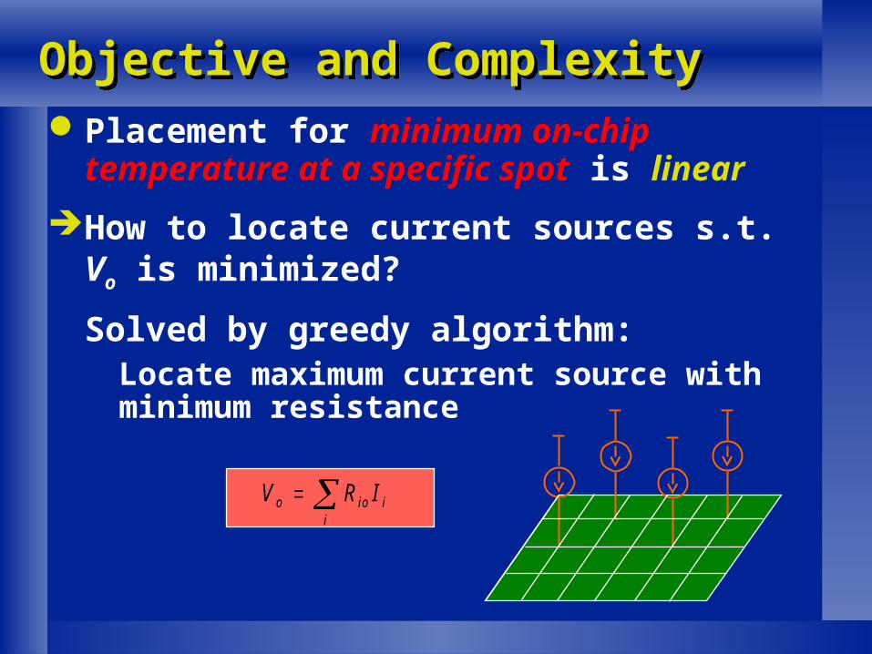
Placement for minimum on-chip temperature at a specific spot is linear
How to locate current sources s.t. Vo is minimized?
Solved by greedy algorithm: Locate maximum current source with minimum resistance
Objective and ComplexityObjective and Complexity
V R Io io ii

Placement for minimum average on-chip temperature is linear
How to locate current sources s.t. iVi is minimized?
Solved by greedy algorithm: Locate maximum current source with minimum resistance
Objective and ComplexityObjective and Complexity
V R Iii
i j jji

Placement for minimum maximum on-chip temperature is NP-hard
Reduces to the bi-partition problem:
Given
we have
Objective and ComplexityObjective and Complexity
V R I
V R I
V
j jj
j jj
i
1 1
2 2
1 2 0
,
R i j
1
0
i=1,2 and i,j on the same side
otherwise
OutlineOutline
Background
Modeling and Theoretical Results
Analytical Thermal Placement
Experiment
Summary

Problem FormulationProblem FormulationGiven
Chip dimensions 0<x<a, 0<y<b, 0<z<d Thermal parameters
Thermal conductivity k on chip top Thermal conductivity kN on chip bottom Effective heat transfer coefficient h on chip bottom Ambient temperature Tr
Cells C of power consumption P Netlist N
Find a cell placement which minimizes sum of total wirelength and maximum temperature
( )nc Cn N
L MaxT c

Analytical PlacementAnalytical Placement Approximate the NP-hard placement problem as a
nonlinear optimization problem
Relax the non-overlapping constraint into a cell density unevenness penalty function
Minimize1 2( )n x
n x
L D D
relax
legalize

A cell centered at (xc,yc) of width w and height h distributes its area over a grid of points (x,y)
where
Cell Density DistributionCell Density Distribution
-r/2 r/2
1
x
Cell density
-r/2 r/2
1
x
Cell density
-r r
d x y w h x y b x x w b y y hc c c c( , , , , , ) ( , ) ( , )
b l r
l
rl
r
l r
r
rl r
( , )( )
( )( )
1 2 02
22
2
2
2
2

Half perimeter wirelength
Approximate min/max by logarithm of sum of exponents
Smooth Wirelength FunctionSmooth Wirelength Function
L M ax x M in x M ax y M in yn i i i i ( ) ( ) ( ) ( )
M ax x a e
M in x a e
ix a
i
ix a
i
i
i
( ) lo g( )
( ) lo g( )
/
/
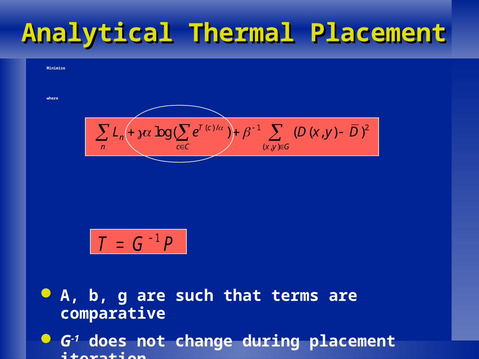
Analytical Thermal PlacementAnalytical Thermal PlacementMinimize
where
( ) / 1 2
( , )
log( ) ( ( , ) )T cn
n c C x y G
L e D x y D
T G P 1
A, b, g are such that terms are comparative
G-1 does not change during placement iteration

Congestion Penalty FunctionCongestion Penalty Function
Minimize
where
( ) / 1log( ) ( )T cn
n c C g G
L e P g
P gD g U D g U
D g U
e
( )( ( ) ) ( )
( )
0
If congested: sharper increase of penalty stricter enhancement
If not congested: no penalty more relaxed

OutlineOutline
Background
Modeling and Theoretical Results
Analytical Thermal Placement
Experiment
Summary

Experiment SettingExperiment Setting
We compare analytical thermal placement to thermal effect oblivious analytical placement APlace
Two industry design test cases of gate array logic in 130nm and 180nm technologies
0.43
0.60
Utilization
10.0W
10.0W
Total Power
180nm25157128II
130nm129013397I
Technology
#rows#blocks#cellsdesign

Thermal Placement Data Flow Thermal Placement Data Flow
Thermal Simulation Netlist
ThermalResistances
Chip DimensionsMaterial, Boundary
Conditions
AnalyticalThermal Placement
PowerProfile
Temperature Reduction

A Snapshot of Placement ResultA Snapshot of Placement Result

Analytical Thermal Placement vs. Traditional Analytical PlacementAnalytical Thermal Placement vs. Traditional Analytical Placement
ATP
APlace
Placer
(s)(%)(mm)(%)(K)
800.5295.39481.5482.159.940.10
636.1392.47466.7892.2311.160.02
718.5392.19465.3597.4711.330.00
0.00
HPWL CPUMax Temp g
Test case II: 180m industry design of 7K cells
Test case I: 130nm industry design of13K cells
ATP
APlace
Placer
(s)(%)(mm)(%)(K)
507.9499.55919.4269.231.890.10
496.9198.03905.3499.632.720.02
98.06905.62109.522.990.00
0.00
HPWL CPUMax Tempg

OutlineOutline
Background
Modeling and Theoretical Results
Analytical Thermal Placement
Experiment
Summary

SummarySummary We propose analytical thermal placement and
achieve 17.85% and 30.77% maximum on-chip temperature variation reduction and 4.61% and 0.45% wirelength reduction compared with the existing analytical placement for the two industry designs, respectively
We present theoretical results on the complexity of specific spot temperature, average on-chip temperature, and maximum on-chip temperature minimum placement as linear, linear, and NP-hard
Future directions Thermal effect aware performance optimization 3-D thermal placement

Thanks for your attention!Thanks for your attention!