analysis of rectifier operation
TRANSCRIPT

Analysis of Rectifier Operation*0. H. SCHADEt, MEMBER, I.R.E.
Summary-An analysis of rectifier operation in principal cir-cuits is made. The introduction of linear equivalent diode resist-ance values permits a simplified and accurate treatment of circuitscontaining high-vacuum diodes and series resistance. The evalua-tion of these equivalent resistance values and a discussion of emis-sion characteristics of oxide-coated cathodes precede the circuitanalysis.
Generalized curve families for three principal condenser-inputcircuits are given to permit the rapid solution of rectifier problemsin practical circuits without inaccuracies due to idealizing assump-tions.
The data presented in this paper have been derived on the basisof a sinusoidal voltage source. It is apparent that the graphic analy-sis may be applied to circuits with nonsinusoidal voltage sources orintermittent pulse waves.
It is also permissible to consider only the wave section duringconduction time and alter the remaining wave form at will. Compli-cated wave shapes may thus be replaced in many cases by a sub-stantially sinusoidal voltage of higher frequency and intermittentoccurrence as indicated by shape and duration of the highest volt-age peak.
The applications of these principles have often explained largediscrepancies from expected results as being caused by series ordiode resistance and excessive peak-current demands.
Practical experience over many years has proved the correct-ness and accuracy of the generalized characteristics of condenser-input circuits.
INTRODUCTION
n ECTIFIER circuits, especially of the condenser-input type, are extensively used in radio andtelevision circuits to produce unidirectional cur-
rents and voltages. The design of power supplies, grid-current bias circuits, peak voltmeters, detectors andmany other circuits in practical equipment is oftenbased on the assumption that rectifier- and power-source resistance are zero, this assumption resulting inserious errors. The rectifier element or diode, further-more has certain peak-current and power ratingswhich should not be exceeded. These values vary con-siderably with the series resistance of the circuit.
General operating characteristics of practical recti-fier circuits have been evaluated and used by the writerfor design purposes and information since early 1934,but circumstances have delayed publication. Severalpapers1-4 have appeared in the meantime treating
* Decimal classification: R337XR356.3. Original manuscriptreceived by the Institute, August 4, 1942; revised manuscript re-ceived, March 9,1943.
t RCA Victor Division, Radio Corporation of America, Harri-son, New Jersey.
l M. B. Stout, "Analysis of rectifier filter circuits," Elec. Eng.Trans. A.I.E.E. (Elec. Eng., September, 1935), vol. 54, pp. 977-984; Septenmber, 1935.
2 N. H. Roberts, "The diode as half-wave, full-wave and voltage-doubling rectifier," Wireless Eng., vol. 13, pp. 351-362; July, 1936;and pp. 423-470; August, 1936.
3 J. C. Frommer, "The determination of operating data andallowable ratings of vacuum-tube rectifiers," PROC. I.R.E., vol. 29,pp. 481-485; September, 1941.
4D. L. Waidelich, "The full-wave voltage-doubling rectifiercircuit," PROC. I.R.E., vol. 29, pp. 554-558; October, 1941.
one or another part of the subject on the assunmptionof zero series resistance. Practical circuits haveresistance and may even require insertion of addi-tional resistance to protect the diodc and input con-denser against destructive currents. The equivalentdiode resistance and the emission from oxide-coatedcathodes are, therefore, discussed preceding the gen-eral circuit analysis. This analysis is illustrated ongraphic constructions establishing a direct link withoscillograph observations on practical circuits. A de-tailed mathematical discussion requires much spaceand is dispensed with in favor of graphic solutions,supplenmented by generalized operating characteristics.
I. PRINCIPLES OF RECTIFICATION
GeneralRectification is a process of synchronized switching.
The basic rectifier circuit consists of one synchronizedswitch in series with a single-phase source of single fre-quency and a resistance load. The switch connectionbetween load terminals and source is closed whensource and load terminals have the same polarity, andis open during the time of opposite polarity. The loadcurrent consists of half-wave pulses. This simple cir-cuit is unsuitable for most practical purposes, becauseit does not furnish a smooth load current.The current may be smoothed by two methods: (a)
by increasing the number of phases, and (b) by insert-ing reactive elements into the circuit. The phase num-ber is limited to two for radio receivers. The circuitanalysis which follows later on will treat single- anddouble-phase rectifier circuits with reactive circuitelements.
Switching in reactive circuits gives rise to "tran-sients. " Current and voltage cannot, therefore, be com-puted according to steady-state methods.The diode functions as a self-timing electronic
switch. It closes the circuit when the plate becomespositive with respect to the cathode and opens the cir-cuit at the instant when the plate current becomeszero.The diode has an internal resistance which is a func-
tion of current. When analyzing rectifier circuits, it isconvenient to treat the internal resistance of the dioderectifier as an element, separated from the "switchaction" of the diode. Fig. 1 illustrates the three circuitelements so obtained and their respective voltage-cur-rent characteristics (see Section II). The diode charac-teristic is the sum of these characteristics. The resist-ance rd is effective only when the switch is closed, i.e.,during the conduction period of the diode. The effec-tive diode resistance must, therefore, be measured orevaluated within conduction-time limits. Consider a
Proceedings of the I.R.E.July, 1943 341

Proceedings of the I.R.E.
switch in series with a fixed resistance and any numberof other circuit elements connected to a battery offixed voltage. The direct current and root-mean-squarecurrent which flow in this circuit will depend on thetime intervals during which the switch is closed andopen; the resistance value is not obtainable from thesecurrent values and the battery voltage. The correctvalue is obtained only when the current and voltage
+ + l
-E O °~ + ° +Ea
SYNCHRO-NIZEDSWITCH
INTER-+ NAL +
POTENTIAL
Id= p'
A
DoEpVEXTERNAELY
I APPLIEDII VOLTAGE
o-I d
DIODEVOLTAGE
E,rd EI r
N0N -
LI NEAR = EQUIVALENT CIRCUITRESISTANCE
Fig. 1 Characteristics and equivalent circuit forhigh-vacuum diodes.
drop in the resistance are measured during the timeangle 4 (Fig. 2) when the switch is closed.The method of analysis of rectifier circuits to be dis-
cussed in this paper is based on the principle that thenonlinear effective resistance of the diode may be re-placed analytically by an equivalent fixed resistancewhich will give a diode current equal to that obtainedwith the actual nonlinear diode resistance. The correctvalue to be used for the equivalent fixed resistance de-pends upon whether we are analyzing for peak diodecurrent, average diode current, or root-mean-squarediode current.At the outset of an analysis amplitude and wave
shape of the diode current are not known and the dioderesistance must, therefore, be determined by successiveapproximations.The complexity of repeated calculations, especially
on condenser-input circuits, requires that the operatingcharacteristics of the circuit be plotted generally asfunctions of the circuit constants including series re-sistance in the diode circuit as a parameter.
Data for these plots (such as Figs. 3 to 7) are to beobtained by general analysis of circuits with linear re-sistances.The solution of a practical condenser-input-circuit
problem requires the use of three different equivalentlinear circuits and diode resistance values.The resistance values are obtainable from the peak
current alone because wave shape can be eliminated asa factor by means of a general relation given by (6).The practical analysis of condenser input circuits thussimplified, is carried out as follows:The average diode current is estimated roughly and
the diode peak current is assumed to be four times theaverage value. The diode characteristic (Fig. 8) fur-
nishes an initial peak-resistance value and (6) furnishesthe other diode resistance values (see R8 values inFig. 9). Direct output voltage and average current arenow obtained with the equivalent average value i,from the respective plot (Figs. 3 to 5) as a first approxi-mation. Another chart (Fig. 6) furnishes the peak-to-average-diode-current ratio with the peak value R8 andthus the peak current and diode peak resistance inclose approximation.A second approximation gives usually good agree-
ment between initial and obtained resistance values,which are then used to obtain other operating data.A theoretical treatment of the method just described
will be omitted in favor of an analysis of operatingcharacteristics of the rectifier tube itself. The user oftubes may welcome information on the subject ofpeak emission which is of vital importance in the ratingand trouble-free operation of any tube with an oxide-coated cathode.
II. ANODE AND CATHODE CHARACTERISTICSOF RECTIFIER TUBES
A node Characteristics1. Definitions of Resistance Values
The instantaneous resistance (rd) of a diode is the ra-tio of the instantaneous plate voltage ed to the in-stantaneous plate current i, at any point on the char-acteristic measured from the operating point (see Fig.1). It is expressed by
edrd = -.
'p(1)
The operating point (0) of a diode is a fixed point onthe characteristic, marked by beginning and end of the
dFd
II I)
I7 ^+
I I.-- lI
- Idi- 0 -1~ 1- o
N-2 11 --
--I
0~~-j --I
_* f _1 i= a-
-ed Deiermined By Crcuif
Fig. 2-Graphic evaluation of equivalent dioderesistance values.
conduction time. It is, therefore, the cutoff point Id = 0and Ed =0, as shown in Fig. 1. The operating point isindependent of the wave form and of the conductiontime 4 (see Fig. 2).
The peak resistance' (id) is a specific value of the in-stantaneous resistance and is defined as
6 For system of symbols, see Appendix.
Jully342

14Schade: Analysis of Rectifier Operation
lbc
2.5
401uj\~ ~~f SC- 0, ;T|A___..li M1iii9igl11IllUlllliill 1
X~~e Th equvaen avrg reitac (td is deie on the; t
Td (see Fig. 2). (2) basis of circuit performance as a resi e v e d-
X < 1iW i T _ . 2 iil i_ i F ! T V
-ermining the magnitud of-theiaverage current in theP v e :-an pa current i.1.are...mar circuit.The value lois,,therefore,the rai of the aver-mteotin in a v r. in e d d n
{ ,; T _I T+FF1111r1111,,,_,,,,,mIIIIIII|I||1b111|1111 llllliiI^IFt4-IL !i! a i 0
's1S -1: i 1111111111111111111lllllllllllll lllllllllli II 11111111wCRL(C IN FARtADS,RL IN OFIMS)
Fig. 3-Relation of applied alternating peak voltage to direct output voltage in half-wave, condenser-input circuits.
ed The equivalent average resistance (rd) is defined on theid = (see Fig. 2). (2) basis of circuit performance as a resistance value de-
termining the magnitude of the average current in thePeak voltage gd and peak current tp are measured circuit. The value ird is, therefore, the ratio of the aver-
from the operating point 0. age voltage drop ed(,6) in the diode during conduction
1943 343

Proceedings of the I.R.E.
10 100 1000,.M.05
43.S
12.5
15
x -.020 LAN
1a:
00
WCRL(C IN FARADS,RL IN OHMS)
Fig. 4-Relation of applied alternating peak voltage to direct output voltage in full-wave, condenser-input circuits.
time to the average current ip(o during conductiontime, or
ed(o)rd =-
iP(o)(3)
The curved diode characteristic is thus replaced byan equivalent linear characteristic having the slope fdand intersecting the average point A, as shown in Fig.2. The co-ordinates Od(,p) and ip,A of the average pointdepend on the shape of voltage and current within thetime angle 4. The analysis of rectifier circuits showsthat the shape of the current pulse in actual circuitsvaries considerably between different circuit types.
The equivalent root-mean-square resistance (frd|) isdefined as the resistance in which the power loss Pd is
equal to the plate dissipation of the diode when thesame value of root-mean-square current JIdl flows inthe resistance as in the diode circuit. It is expressed by
Pd
II drI2(4)
2. Measurement of Equivalent Diode ResistancesThe equivalent resistance values of diodes can be
measured by direct substitution under actual operatingconditions. The circuit arrangement is shown in Fig.10. Because the diode under test must be replaced as awhole by an adjustable resistance of known value, asecond switch (a mercury-vapor diode identified in thefigure as the ideal diode) with negligible resistance
344 July

Schade: Analysis of Rectifier Operation
Illlllllllllllii -------------1....
.~~~~~~~~~~~~~~~~~~~~~~~~~~~~ _............8
120- 11X 1 .1 0 0
WCRL(C IN FARAOS,RL IN OHMS)
Fig. 5-Relation of applied alternating peak voltage to direct output voltage in condenser-input, voltage-doubling circuits.
must be inserted in order to preserve the switch-action observation remains unchanged for both positions ofin the circuit. the switch S. We observe (1) that it is impossible toWhen a measurement is being made, the resistor Rd find one single value of Rd which will duplicate condi-
is varied until the particular voltage or current under tions of the actual tube circuit, i.e., give the same
3451943

346
33
Proceedings of the I.R.E. July
71 U
lll .,.,,,,............. ,, .... .- - - .-- ..-
0_a . i att . .O_ . oo e0 (31.esd3NO)'N33B"nv31V'd SWv = I (31rcd 3NO) lN3dnO 33 V5d O-a = I±)N3t,A,n: 3.Lv'1d 3-o , N3~ufn 3.LVId 3-O
3.LVId 3Nu IN3t t6, j3.lVi SINS - I-I (1 d /3N)IN3wunA, 3.LVId W43d =~iV
values of peak, average, and root-mean-square current 3. Wave Forms and Equivalent Resistance Ratios forin the circuit; (2) that the ratio of these three 'equiva- Practical Circuit Calculationslent" resistance values of the diode varies for differentcombinations of circuit elements; and (3) that the The form of the current pulse in practical rectifier.resistance values are functions of the current ampli- circuits is determined by the power factor of the loadtude and wave shape. circuit and the phase number. Practical circuits may be

Schade: Analysis of Rectifier Operation
0
0.
ml
10007"'I -s'''"- '3X 40 50wX07810 100
(OCRL(C IN FARADS, RL INOHMS)
Fig. 7-Root-mean-square ripple voltage of condenser-input circuits.
divided into two main groups: (a) circuits with choke-input filter; and (b) circuits with condenser-inputfilter.
The diode current pulse in choke-input circuits has a
rectangular form on which is superi.nposed one cycleof the lowest ripple frequency. In most practical cir-cuits, this fluctuation is small as compared with theaverage amplitude of the wave and may be neglectedwhen determining the equivalent diode resistances. Itis apparent then that the equivalent diode resistancevalues are all equal and independent of the type ofdiode characteristics for square-wave forms. Hence, forchoke-input circuits, we have
; = Td = | rd |. (5)
The diode current pulse in condenser-input circuits isthe summation of a sine-wave section and a currenthaving an exponential decay. It varies from a triangu-lar form for 4 < 20 degrees to a full half cycle (4 = 180
degrees) as the other extreme. In Table I are given theratios of voltages, currents, and resistance values dur-ing conduction time for two principal types of rectifier
TABLE I
3/2-Power RectangularConduc- Rectifier Characteristic
tion Wave CharacteristicTime ShapeAngle ip(5) |ip,(,|) ido d I|rdl d(O)| rd I ltd
tp fp td |'rd d 2d d |i
Condenser-Input Circuits
Degrees I
<20 0.500 0.577 0.593 1.185 1.120 1.0 2.00 1.500
90saond 0.637 0.707 0.715 1.120 1.057 1.0 1.57 1.272
130 0.725 0.78010 787 1.085 1.030 1.0 1.38 1.190
Choke-Input Circuits
180 ..FL 1.0 1.0 1.0 1.0 1.0 1.0 1.0 1.0
3471943

Proceedings of the I.R.E.
characteristics: the 3/2-power-law characteristic ofhigh-vacuum diodes, and the idealized rectangularcharacteristic of hot-cathode, mercury-vapor diodes.In this table, the designation lip, (0) represents theroot-mean-square value of the current during the con-duction time.
It follows that the relation
;d = 0. 88rd = 0. 93 | rd I (6)
is representative for the group of condenser-input cir-cuits containing high-vacuum diodes, and holds within± 5 per cent over the entire range of variation in wave
,-2i L'i i S iT i i CU2X2 L
S~~~~~~~~~~~~~~~~~~~~~~~~~U-I~~~~~~~~~~~~~~~~~~~~~~~~~~~~~~~~~~~~~~~~~~~~~~~~~~~I
! ^ 2 ffi .+ i X4-6 F
252 A
2 : it : . 1 ~. A'
when heated, supplies the electron cloud forming thespace charge above the coating surface (see Fig. 11).The emission from this surface may have values ashigh as 100 arnperes per square centimeter. The flowof such enormous currents is, however, dependent onthe internal-coating impedance and is possible onlyunder certain conditions. Special apparatus is required
lip'IDEA -OR I DIODE llp
t
FULL-WAVE CIRCUIT
DIODE VOLTS = Eo + pFig. 8-Average anode characteristics of some RCA rectifier tubes.
shape. The actual error in circuit calculations is smalleras the diode resistance is only part of the total seriesresistance in the circuit.
CATHODE CHARACTERISTICSPeak-Emission and Saturation of Oxide-Coated CathodesThe normal operating range of diodes (including in-
stantaneous peak values) is below the saturation po-tential because the plate dissipation rises rapidly todangerous values if this potential is exceeded. Satura-tion is definitely recognized in diodes with tungsten orthoriated-tungsten cathodes as it does not depend onthe time of measurement, provided the plate dissipa-tion is not excessive. The characteristics of such diodesare single-valued even in the saturated range, i.e., therange in which the same value of current is obtainedat a given voltage whether the voltage has been in-creased or decreased to the particular value.
Diodes with oxide-coated cathodes may have double-valued characteristics because of the coating character-istic. The cathode coating has resistance and capaci-tance, both of which are a function of temperature,current, and the degree of 'activation."A highly emitting monatomic layer of barium on
oxygen is formed on the surface of the coating, which,
rd=.e8d= .935IrI R'P
R5= EXTERNAL RESISTANCE_fl~~__._ISTANCEaRS 1 ;:; r4d. PAK UIODE REMII
PS RS + frd~L E.-I . EQUIVALENT AVE. I
IRsI = RS+ Irdl |j-dJOEQUIWILENT R S S
*USE rS~,O1 I|RSI AS REQUIRED
Fig. 9-Equivalent circuits and resistance values forcondenser-input rectifier circuits.
VOLTAGE-DOUBLING CIRCUIT
CONTACTPOTENTIAL\ 0 APPLIED PEAK
IO; e PVOLTAGE
e DI P OL
DIODE PEAK VOLTAGE
STANCEDIODE RESISTANCE
DIODE RESISTANCE
348 July

Schade: A nalysis of Rectifier Operation
to permit observation of high current values which, toprevent harmi to the tube, can be maintained only oververy short time intervals determined by the thermalcapacity of the plate and coating. For example, an in-stantaneous power of 15 kilowatts must be dissipatedin the close-spaced diode type 83-v at a current of 25amperes froml its cathode sturface of only 1 squiare cen-timeter.
60-IDEAL OIODEFOR LARGER
g 10-V. fi UiNvDEntR
f" ~~~~~~~~EoEF OSC ILLOGRAPH i
TO MEASURE T,,
RMS CURRENT _IOA AV. CURRENT
R-t LOAD -
Fig. 10-Circuit for measuring equivalent dioderesistance values.
Equipment for such observations was built in June,1937, by the author after data obtained in 1935 on alow-powered curve tracer6 indicated the need for equip-ment having a power source of very low internal impe-dance for measurements on even relatively small diodes.
1. Measurement of Diode Characteristics and PeakEmissionThe circuit principle is shown in Fig. 12. The second-
ary voltage of a 2-kilovolt-ampere transformer Tm is6 Demonstrated, Rochester Fall Meeting, Rochester, N. Y.,
November 18, 1935.
adjustable from zero to 2 kilovolts by imieans of ainlautotransformer TA. Transformer and line reactancesare eliminated for short-time surge currents by a largecondenser load (C=20 to 80 microfarads). The largereactive current is "tuned out" by a choke L of con-
*.. *7sSPACE CHARGE
; ~~~~~~~~~MONA1OMI C
W,,0EtR ,,,\,\N',,,2&,x,, LAERY OFN//i\~ \,'r~M~)\' '/1; BARIUM
\/',, ~\ /1 / 1,1 0.,\~\"'7'K"~ OXIDES
FBASE METAL
Fig. I11 Representation of cathode coating.
YQ&Qj
r3TYPEr3API/906 -Pl
Fig. 12 Peak emission test circuit.
siderable size. The voltage is applied through a largemercury diode and a synchronous contact arrangementm to the tube under test in series with a resistance boxR8 and a condenser input load CL and RL. This load
eMAX. 495 VOLTS 16,j.f2 KT SCJ..RL e RL= 2500 OHMSe2fis GD2 17.9I RS = 500 OHMS
SLMAX. =.922 AMPEREFS i
Fig. 13Starting conditions in a full-wave, c'ondenser-input circuit with large series resistance.
1943 349

Proceedings of the I.R.E.
permits adjustment of the peak-to-average currentratio. Variation of RL changes the average current.Variation of CL and phasing of the synchronous con-tact m with respect to the 60-cycle line voltage permitregulation, within wide limits, of the rate of change andduration of the current pulses.
. 501
so 00 I5O' L
I~~~~~~22~
° ed-VOLTS -120 SCTY
NEGATIVE A-C VOLTAGE EBIAS E PARAMETER
POOR COATING CONDUCTANCE
I.tI
CATHODETEMPERATURE=PARAMETER
(b)
ed-VOLTS
CONDUCTANCE TEMPERATURt LIMITED
(c)
50 00 Iso HEATER VOLTAGLed-VOLTS OF DI = PARAMETER
ARTIFICIAL DIODE CHARACTERISTIC
Fig. 14-Double-valued characteristics of actual and artificialdiodes showing coating saturation.
The dynamic voltage-current characteristic of thetube under test is observed on a cathode-ray oscillo-graph connected in the conventional manner. Calibra-tion deflections are inserted (not shown) by other syn-
chronous contacts to provide accurate and simultane-ously visible substitution co-ordinates which may bemoved to any point in the characteristic.The motor-driven synchronous contactor closes the
circuit at a desired instant of the line-voltage cycle.The circuit may then be maintained closed for approxi-mately 30 cycles to allow decay of the starting tran-sient (see Fig. 13). It is then opened for approximately70 cycles to allow time for the discharge of condenserCL. This cycle repeats continuously. The diode Ds in
series with the tube under test protects it against dam-age in case it breaks down or arcs, because the diodetakes up the inverse voltage if a given small reversedcurrent determined by R1 is exceeded. This condition isindicated by a small glow tube in shunt with Ds.
2. Coating CharacteristicsA theory of electron movement and conditions in
oxide coatings has been formulated after careful analy-sis of saturation characteristics observed on the curve
tracer. As saturated coatings produce closed reactiveloops in the characteristic, it is found necessary to as-
sume the existence of a capacitance in the diode itself.Because of its large value (see Fig. 14 (c)), this capaci-tance requires a dielectric thickness approaching crys-tal spacing and, hence, must be located inside thecoating. It is beyond the scope of this paper to reportthe many investigations which led to this. particularconception.The oxide coating is an insulator at room tempera-
ture. At increased temperatures, it becomes conductive(normal operating temperatures are between 1000 and1100 degrees Kelvin). Electronic conduction may bethought of as occurring by relay movement of elec-trons under the influence of electrostatic potentials inthe coating, which is a layer containing insulating oxidecrystals (shaded areas in Fig. 11) interposed withmetal atoms and ions (circles). These have been pro-duced during the activation and aging processes byhigh cathode temperature and electrolysis. The re-quired potential gradients can be produced by rathersmall potentials because of the minute distances in thestructure; the potential drop throughout the coating,therefore, is low under normal conditions.The conduction is high, when a sufficient number of
relay paths not broken by oxides have been formed andwhen electron movement is facilitated by the looseningof the atomic structure which takes place at increasedtemperatures.The coating is not necessarily a homogeneous con-
ductor as it may consist of many sections operating inparallel but having different conductance values with
I.0-
FULLY EMITINGSURFACE LAYER
0.75- PARTIAL TEMPERA-TURE -LIMITED
V% /SURFACE LAYER
a.0.50'
0.25 V
0100 200
Ed-VOLTS
Fig. 15-Single-valued diode characteristics.
individual temperature parameters. At increased platepotentials, poorly conducting sections tend to saturate,the section potential becoming more positive towardsthe surface. Negative-grid action of neighboring sec-tions with higher conductivity may tend to limit emis-sion from the surface over the poor section but theincreased positive gradient towards the saturating sec-tion causes it to draw electrons from the surroundingcoating towards its surface. Further increase in cur-rent demand may then saturate the better conductingpaths and may even fuse them, thus forcing current
350 Jilly

Schcade: Analysis of Rectifier Operation
through poorer sections. Forced electron flow resultsin local power dissipation and temperature increasesand may cause ionization and electrolysis accompaniedby liberation of gas (oxygen) and formation of bariummetal; i.e., it causes an accelerated activation process.These conditions in the diode coating, therefore,
should furnish a voltage-current characteristic ofpurely ohmic character as long as activation-gas liber-ation is substantially absent. Characteristics of thistype are single valued. Single-valued characteristicsindicate, however, unsaturated ohmic coating con-ductance and limiting surface emission when moderate-current densities are involved as will be apparent fromthe following discussion. As cathode and coating tem-peratures are relatively slowly varying parameters,characteristics such as shown in Fig. 15 are observedon the cathode-ray curve tracer. The characteristic
permit a total emission current of short duration muchin excess of the possible steady-state conduction cur-rent. The "transient-emission" current depends on theeffective capacitance value of the blocking oxides, theirseries and shunt conductance in the coating, the emis-sion and area of corresponding surface elements to theplate as well as on the external plate-circuit impedance,and the wave form of the applied plate voltage.
For the purpose of analysis, therefore, we may drawrepresentative networks such as shown in Figs. 17 or
= t 1PLATE-VACUUM
F- r-I-SURFACE
- PLATE-VACUUM
I I -I-SURFACE
4040-rp=o
z 30-
2I 20-J
1 10-
-, ,-5 10°
Ep- VOLTS
El _-41 (a)
Ep-VOLTS
(b)
11- 11+ /rs
EQUIVALENT CIRCUITS
OR r
rd (C)
Fig. 16-Characteristics and equivalent circuit forhot-cathode, mercury-vapor diodes.
of diodes containing larger amounts of gas exhibits adiscontinuity or "gas loop" (compare Fig. 16 (b))which is recognized by the fact that correspondingcurrent values after ionization require less diode po-tential than before "breakdown." The characteristic,hence, is steeper than normal.
3. Transient EmissionLet us now consider the action of insulating oxides
in the coating. They block many possible electronpaths to sections of the surface layer which, therefore,cannot emit steady electron currents. However, elec-trons can be moved to the oxide surfaces and a dis-placement current can flow in these coating sectionsallowing transient-emission currents to be drawn fromthe corresponding surface sections.The displacement current in the coating and the
corresponding transient surface emission represent acertain fraction of the total diode current, which may
Fig. 17 (left)-Circuit network representing thecoating impedance in high-vacuum diodes.
Fig. 18 (right)-Same as Fig. 17 with resistancesreplaced by special diodes.
18 and show the temperature-controlled coating con-ductances r, as a network of "close-spaced diodes"which may conduct in two directions, each one havinga single-valued characteristic which may be unsatu-rated or saturated depending on the assumed condi-tions in the coating; the conductance values of these"diodes" depend on the number of parallel or seriespaths they represent.The diode contains, therefore, in its coating, a type
of condenser-input load circuit, which is analyzedlater on in this paper; its action explains double-valuedvoltage-current characteristics obtainable from thediode alone.
Consider a high plate voltage suddenly applied bymeans of a switch to a diode as in the circuit of Fig. 19.
i =Ic+ it
__
-}TIME
(a) (b)
Fig. 19-Circuit for observation of peakemission transients.
If the coating is not limiting, the current obtained isthat at a point P on the corresponding diode character-istic. Hence, the current wave form in the circuit is asshown in Fig. 19(a). If the surface emission is assumedto be unchanged, but the coating conductance is lim-ited, due to an insufficient number of "coating diodes"and too many nonconducting oxide groups, the waveform of Fig. 19 (b) is obtained. At the instant whenthe switch is closed the current value i is demanded byEd from the surface layer; the conduction current inthe coating is limited to the value 1, by saturation of
35'11943

Proceedings of the I.R.E.
the "coating diodes." Because of the oxide capacitance,a displacement current can flow and charge up theoxides, but their charge may be limited by hypotheti-cal series diodes.The coating resistance is extremely low7 below satu-
ration, but becomes infinite when the conduction cur-
rent is saturated; the charging current must then flowin the plate circuit (external) of the diode. The totalplate current is, therefore, the sum of the conductioncurrent I and a "transient-emission" current. The"coating transient" decays to zero the same as normaltransients at a rate depending on the actual shunt-conductance value and the total series resistance in thecircuit (Fig. 19(b)). The decay can be changed by add-ing external resistance in the plate circuit. When thesurface emission is good, i.e., as long as the total vac-
uum-space plate current is space-charge-limited, thecurrent will rise initially to the value (point P) deter-mined by the applied potential, but will then decay tothe saturation value determined by the coating con-
ductance.The condition of oxide-coated cathodes can, there-
fore, not be judged alone by their capability of furnish-ing high peak currents, but the time of current flowand the current wave form must also be carefully con-
sidered, because the diode characteristic may not besingle-valued. Fig. 14 shows characteristics which are
not single-valued. It should be noted that the charac-teristic loops are formed in the opposite sense as gas
loops. Their extent depends on the time interval in-volved and the current value exceeding the unsatur-ated conductance current. An artificially producedcharacteristic of this type is also shown in Fig. 14(c).The loop size can be varied by adjusting the cathodetemperature of the shunting diode. Both diodes hadsingle-valued characteristics.
4. Current Overload and Sputter
The degree of activation is not stable during the lifeof the cathode. Coating conductance and surfaceemission change. Factors affecting the change are thecoating substances, the evaporation rate of bariumwhich depends on the base material, and the operatingconditions to which the cathode is subjected. This lifehistory of the cathode is the basis on which current
ratings are established. Rectifier tubes especially are
subject to severe operating conditions. If a diode is
operated with too high a current in a rectifier circuitand its surface emission is decreased to the saturationvalue, then the tube-voltage drop will increase rapidlyand cause excessive plate dissipation and destructionof the tube. Should the coating conductance in this
diode decrease to a value which limits the demandedcurrent, power is dissipated in the now-saturated coat-ing with the result that the coating-voltage drop andcoating temperature are raised. The voltage and tem-
7 Its magnitude depends on the number of series diodes and,hence on the barium content and thickness of the coating.
perature rise in the coating may cause reactivation butalso may become cumulative and melt the coatingmaterial. We may consider that good conducting pathsare fused or that a dielectric breakdown of oxide ca-pacitance occurs; in any event vapor or gas dischargesresult from saturated coatings. In most cases break-down occurs during one of the following inverse voltagecycles as observed on the curve tracer. A saturationloop is first formed as shown in Fig. 14 and a certaintime must be allowed for diffusion of the gas into thevacuum space. Fusion of coating material may alsooccur during the conduction period. These breakdownsare known as "sputter," and in usual circuits destroythe cathode.A second type of sputter is caused by the intense
electrostatic field to which projecting "high spots" onthe plate or cathode are subjected. The resulting cur-rent concentration causes these spots to vaporize withthe result that an arc may be started. Hundreds ofscintillating small spots can be observed at first atvery high applied surge potentials, but may be clearedafter a relatively short time.
Transient peak currents of 25 amperes per squarecentimeter have been observed from well-activatedoxide-coated cathodes. The stable peak emission overan extended period is usually less than one third ofthis value.
5. Hot-Cathode Mercury- Vapor Diodes
The breakdown voltage Ei of mercury vapor forcumulative ionization is a function of the gas pressureand temperature. It is approximately 10 volts in theRCA-83 and similar tubes. A small electron currentbegins to flow at Ep =0 (see Fig. 16), and causes ioniza-tion of the mercury vapor. This action decreases thevariational diode resistance rp to a very low value.The ionization becomes cumulative at a certain cur-rent value (rp=0 at 40 milliamperes in Fig. 16(a)),and causes a discontinuity in the characteristic. Hence,it is not single-valued within a certain voltage range.Beyond this range (see Fig. 16(b)), the slope (rp) ofthe characteristic becomes again positive until satura-tion of the emitter is reached.
For circuit analysis, the mercury-vapor diode maybe replaced by a bucking battery having the voltageEi and a fixed resistance as shown in Fig. 16(c); or thediode characteristic may be replaced by an ideal rec-tangular characteristic and its equivalent resistancevalues and the series resistance rd, as shown.The first representation is adequate for most prac-
tical calculations. The value rd, is in the order of 4 ohmsfor small rectifier tubes. The low series resistance andthe small constant-voltage drop Ei are distinct ad-vantages for choke-input filters, as they cause verygood regulation; the low resistance, however, will giverise to enormously high starting transients in con-denser-input circuits, in case all other series resistancesare also small. The destruction of the coating in
352 July

Schade: A nalysis of Rectifier Operation
mercury-vapor diodes is caused by concentration of cur-rent to small sections of the coating surface and not byheat dissipation in the coating. Mercury-vapor diodesas well as high-perveance (close-spaced), high-vacuumdiodes having oxide cathodes should, therefore, be pro-tected against transient-current overloads when theyare started in low-resistance circuits to prevent de-struction of the cathode coating.
6. Protective Resistance Values.Very high instantaneous peak currents may occur
in noninductive condenser-input circuits when the cir-cuit is opened long enough to discharge the condenser,but reclosed before the cathode temperature of thediode has decreased substantially. The maximum peakcurrent 7max occurs when closing the circuit at peakline voltage. At the instant of switching, C is a shortcircuit and the current 7max is limited only by theseries resistance (including diode) of the circuit,
e maxImax =
R,For a given maximum diode current ldmax and the cor-responding diode peak voltage Edmax, the minimumeffective series resistance R. in the circtuit must hencebe
e max - Edmax
Idmax
This limiting resistance must be inserted in series withlow-impedance sources (power line in transformerlesssets). Commercial power transformers for radio re-ceivers have often sufficient resistance besides someleakage reactance to limit starting currents to safevalues.
III. CIRCUIT ANALYSISGeneralThe rectifier diode is a switch operated in syn-
chronism with the applied alternating-current fre-quency. Switching in reactive circuits causes tran-sients. The total current in the circuit may be regardedas the sum of all steady-state currents and transientcurrents within the time between two switching opera-tions. Steady-state voltages (eS) and currents (is) in theparticular circuit before and after switching are deter-mined without difficulty. It is very helpful to drawthem approximately to scale and with proper phaserelation.The switching time of the diode is then located on
the graph. Currents change at switching time to fromil to i2-is(2)+it and voltages from ei to e2=e8(2)+et.The transients it or et are zero, when the currentchange does not occur in an inductive circuit or whena voltage change is not required on a capacitance atthe time of switching. A sudden change AiL or Ae,demanded at to causes transients. They initially cancelthe change AiL or Ae, because an inductance offersinfinite impedance to an instantaneous change in total
current and a capacitance offers zero impedance to aninstantaneous voltage change.The initial transient values are, therefore,
it(O) in L = -A iLand
et(o) on C = - Ae,.
The transients decay exponentially from their initialvalue.
According to the decay time of the transients, funda-mental rectifier circuits may be classified into twoprincipal groups: (1) circuits with repeating transientsin which the energy stored in reactive elements de-creases to zero between conduction periods of thediode; and (2) circuits with chain transients in which(a) the magnetic energy stored in the inductance ofthe circuit remains above zero value, and (b) the elec-tric energy stored in the capacitance of the circuit re-mains above zero value. The much used "choke-input"and "condenser-input" circuits fall under the secondgroup.We shall analyze the operation in important cir-
cuits, i.e., the full-wave choke-input circuit and con-denser-input circuits.
1. The Full-Wave Choke-Input Circuita) Operation of circuits with L and R, in the common
branch circuitCircuit and operation are shown in Fig. 20. The
analysis is made by considering first one of the diodesshort-circuited to obtain the phase relation of the al-ternating voltage e, and the steady-state current !,, asshown. If we assume that the diode D1 closes the circuitI at the time e=0, a transient it with the initial valueit(o) =-s(o) will flow in the circuit. The total currenti is the sum of the currents -l+it. It starts, therefore,at zero and rises as shown until the second switchingoperation occurs at the commutation time t=7r whenthe second diode D2 receives a positive plate voltage.The total current i in circuit II after t =w7r is again thesum of currents i82+it (Ts2 has reversed polarity withrespect to T,j and is not shown in Fig. 20) but theinitial value it(o) of the second transient is increasedby the value i(,) now flowing in the common circuitinductance L.The current it(o) increases, therefore, at every new
switching time until the decay of the transient it(n),during the time t =7r, is numerically equal to thesteady-state current rise 2iS(o). For the final operatingcurrent at the nth commutation time (see right sideof Fig. 20)
(i(nir) - s(O))(1 - E-RSI2FL) = - 28 (0)
i(n7r) = is(o) - (2s /(o)1i - E-Rs/2FL). (7)
A broken line is shown connecting all commutation-current values. This line represents closely the averagecurrent I in the common circuit branch. The finalaverage current 7 in the load resistance R8 is given by
1943 353
Rs =

Proceedings of the I.R.E.
(7), when the transient decay i,(,) during the time r(Fig. 20) can be regarded as linear (low steady-state power factor of circuit). The average plate cur-rent per diode is I,=0.57, since each diode conducts
b) The full-wave choke input circuit with capacitance-shunted resistance loadFor large capacitance values the by-passed load re-
sistance RL of practical circuits is equivalent to a
t tw
lrL._a_I
D, /CIRCUIT I
2D R L
CIRCUIT LE
° T 21 3w 4w 5wTIME --
Fig. 20-Starting and operating conditions of an
alternately, and passes a current pulse shown by theshaded area in Fig. 20. With the numerical values ofthe circuit Fig. 20 substituted in (7) we obtain
i(nr)- I = 0. 298 ampere.
The oscillogram in Fig. 21 was taken on circuit Fig. 20.
Fig. 21-Oscillograms taken with circuit of Fig. 20.
WI =e2=495 SiNCatc = 377L =14.5 HENRIESR = 1050 OHMS } Zt60_) =5560 OHMS
tse7.=.089 A
0 = 79.1 °
bit 7v
aperiodic full-wave, choke-input rectifier circuit.
battery having a voltage TB = IRL, where I is theaverage load current or battery-charging current. Thecircuit operation (see Fig. 22) is described by obtaining7 as a function of EB. The final commutation currenti(.,) which is closely the average current 7 is given by
I - i(_ = (7B + i.(o)) - 2i.(o)/(1 - e-R.12FL) (7b)and similar to (7) except for an increase of the tran-sient term due to the battery current 7B = EB/R,.
Equation (7b) is valid only over a range of load orbattery voltage (TB) in which switching time andconduction period of the diodes are constant (q =7r).This range is shown by the solid part of curve F inFig. 22 and ends at a particular current and voltageof the circuit characteristic marked the "critical point."
The critical point is the operating condition at whichthe instantaneous current i in the common branchcircuit has zero value at one instant. An analysis showsthat in the range EB = j.. to EB = EB' each diodecircuit operates independently as a half-wave rectifiercircuit (battery-charger operation, curve H in Fig. 22).Current commutation begins at EB'; the diode cir-cuits begin to interact, but the conduction angle isstill 4 <7r.The conduction angle increases from q = 0 at
EB = emDX to 4 = 7r at the critical point EB" which marksthe beginning of chain current operation.
354 July

Schade: A nalysis of Rectifier Operation
T'he critical operating condition is obtained bysolving for i=O with 0=7r or by equating the directcurrent to the negative peak value of the total alter-nating current in L. The critical point is hence specifiedbv a certain current or by a certain ratio K of direct-
500- eMAX.
BEGINNING OF CURRENTIl \ COMMUTATION--
e 400J E \ CRITICAL POINTO e \ /BEGINNING OF TOTA3-oF i xCHAIN CURRENTS-*-- E
- 300 L -NH
N.2I OFHALF-WAVE\ < OPERATION -
RANGE WITHOUT NCOMMUTATION \
If we neglect harmonics higher than 2F, which con-tribute little to the peak value because of phase shiftand increasing attenuation in L, the peak ripple cur-rent (equation (10)) becomes
imjn = 4/37r(jmax/Z(2F))
FULL WAVE(CHAIN-CURRENT
FORMULA)
e 495 SiN wtco= 377RS= 110 OHMSL = 14.5 HENRIES9 = 88.9°
0 20 40 60 80 100AVERAGE CURRENT I - MA.
Fig. 22-Operating characteristic of a full-wave, choke-input rectifier circuit with battery loadEB or resistance load RL =-EB/7 shunted by a large capacitance.
_ K -."Ia2f ,-f-2Yf CRITICAL LOAD-CONDITION OF CIRCUIT
AS SHOWN ABOVE WITH THE FOLLOWINGAL LOAD-CONDITION VALUES:CIRCUIT ABOVE =495 SIN 377t
Rs = 3770 OHMSL = IOHENRIES,caL = 3770 OHMS0=45°
Fig. 23 (left)-Graphic solution for the critical load condition withnegligible series resistance.
Fig. 24 (right)-Same as Fig. 23 but with large series resistance.
current resistance to alternating-current impedance inthe circuit. With reference to the equivalent circuittreated in the following section, a relation to the funda-mental alternating-current component of the rectifiedcurrent (see (10)), i.e., to the impedance Z(2F), atdouble line frequency is more useful. We set, therefore,
(R8+ RL) K (8)
Z (2F)
and determine significant values of K for particularcircuit impedance conditions.
and setting it equal to the average current
I = 2/7r (eiax/(R8+RL))
we obtain K = 1.5 for the ratio as shown in (8).The exact solution for the critical current can be
obtained from a graphic analysis by simple reasoningfor the case R8=O. The general solution will only beindicated. It is obtained by drawing the comple-mentary curve (1-it) of the total transient beginningat the time e=O (see Figs. 23 and 24) and shifting itupward until it touches the current i8, thus solving
CRITICiOF
1943 355
Proceedings of the I.R.E.
for i=0 at the point of contact. Note that i(n) is thesame at to and r in both cases shown.
For R8=0, the transient section becomes a straightline having the slope 2/7r and running parallel to thepeak-to-peak connecting line of !,. The sine-wave slope217x = -cos x gives the point of contact at X = 50.4 de-grees (Fig. 23), and the peak ripple current is obtainedfrom
/ ~~50 4\imin = Isnax siSn 50.4 - --) = 0.21iisiiax
e max= 0.211
wL
Equating this value to the average current given by(10), we obtain the value K=1/0.211=1.51 for cir-
RS L
LA c
~~~~~~RL
COMMUTATEDSINE-WAVE GENERATOR
(0)
E@ ~~C R,4
E 2
C ((b)
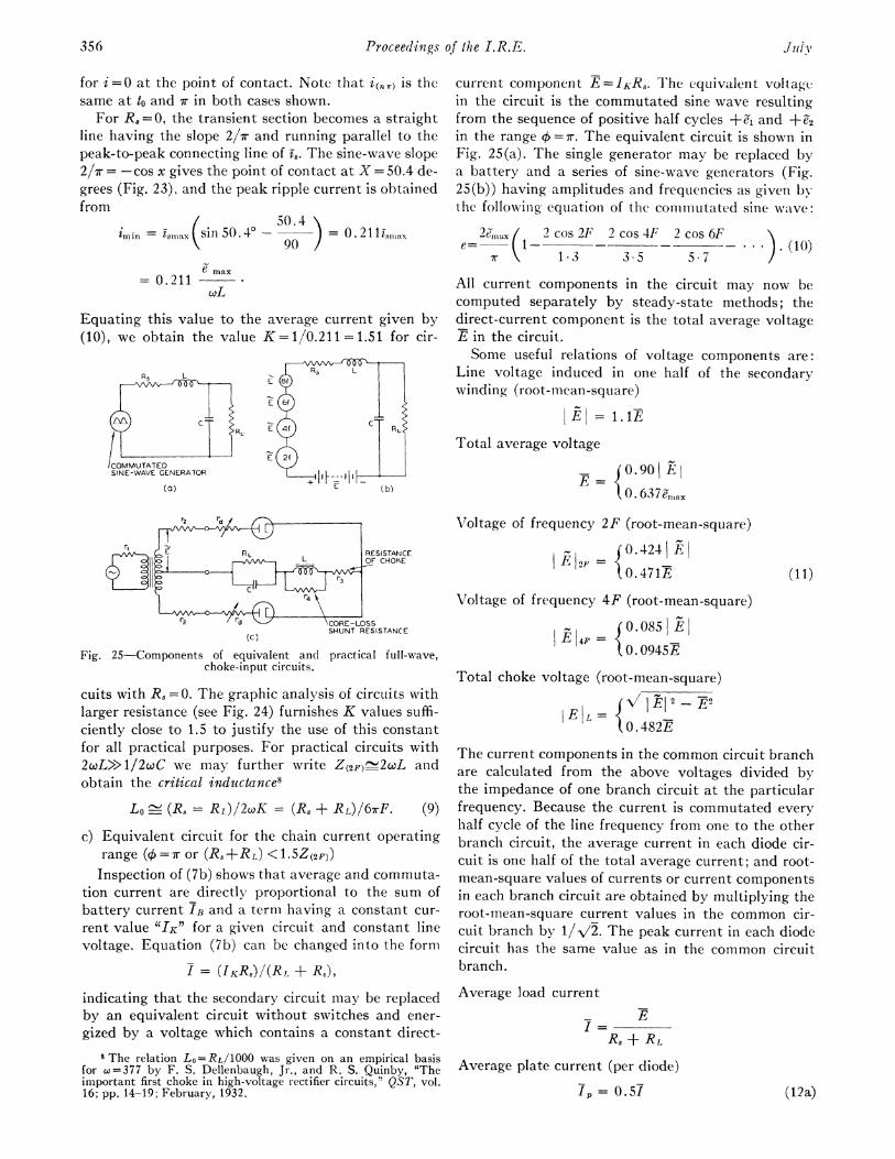
current component E=IKR8. The equivalenit voltagein the circuit is the commutated sine wave resultingfrom the sequence of positive half cycles +ji and +e2in the range X =7r. The equivalent circuit is shown inFig. 25(a). The single generator may be replaced bya battery and a series of sine-wave generators (Fig.25(b)) having amplitudes and frequencies as given bythe followinig equationi of the commllutated sine wave:
2e=jaX (2 cos 2F 2 cos 4F 2 cos 6F )e=- 1- . . (I10)
1r 1- 3 3. 5 5 .7
All current components in the circuit may now becomputed separately by steady-state methods; thedirect-current component is the total average voltage7E in the circuit.Some useful relations of voltage components are:
Line voltage induced in one half of the secondarywinding (root-mean-square)
E = 1.IT
Total average voltage
- 1°0.90 EX,0. 637jyijax
Voltage of frequency 2F (root-mean-square)
E2I2F = {0. 471E
(C)
Fig. 25-Components of equivalent and practical full-wave,choke-input circuits.
cuits with RS=0. The graphic analysis of circuits withlarger resistance (see Fig. 24) furnishes K values suffi-ciently close to 1.5 to justify the use of this constantfor all practical purposes. For practical circuits with2coL>1/2wC we may further write Z(2F){ 2wL andobtain the critical inductance8
LO (RS = RL)/2wK = (RS+ RL)/67rF. (9)
c) Equivalent circuit for the chain current operatingrange (q =r or (R, +RL) < 1*5Z(2F))Inspection of (7b) shows that average and commuta-
tion current are directly proportional to the sum ofbattery current IB and a term having a constant cur-
rent value <IKt for a given circuit and constant linevoltage. Equation (7b) can be changed into the form
I = (IKR.)/(R,, + R8 ),
indicating that the secondary circuit may be replacedby an equivalent circuit without switches and ener-
gized by a voltage which contains a constant direct-
8 The relation Lo=RL/1000 was given on an empirical basisfor wo=377 by F. S. Dellenbaugh, Jr., and R. S. Quinby, "Theimportant first choke in high-voltage rectifier circuits," QST, vol.16; pp. 14-19; February, 1932.
Voltage of frequency 4F (root-mean-square)
|E| 0.0851 E|
0. 0945E
Total choke voltage (root-mean-square)
EIL ElI2 - 2
0.482E
The current components in the common circuit branchare calculated from the above voltages divided bythe impedance of one branch circuit at the particularfrequency. Because the current is commutated every
half cycle of the line frequency from one to the otherbranch circuit, the average current in each diode cir-cuit is one half of the total average current; and root-mean-square values of currents or current componentsin each branch circuit are obtained by multiplying theroot-mean-square current values in the common cir-cuit branch by 1/A/2. The peak current in each diodecircuit has the same value as in the common circuitbranch.
Average load current
I=RS + RL
Average plate current (per diode)
p= 0.5I (12a)
(1 1)
356 Jlfiv

Schade: A nalysis of Rectifier Operation
Double-frequency current (root-mean-square) in com-mon circuit branch
17 2 E 2F
Z(2F)TFotal current (root-miean-square) in common circuitbranch
IIL=\7I2+II122FRoot-mean-square diode current or root-mean-squarecurrent per transformer winding
= /II (12b)
Peak diode current
z= 1+ (ilr2P X V/2)
I-1-1
0
0
llJ
Ja.
D
Ihe regulation curve for a circuit with high-vacuumldiodes is the sum of the 3/2-power-law diode charac-teristic and the ohmic series resistance r2 of one branchcircuit as shown in Fig. 26. The curve is correct forconstant voltage e and beyond the critical currentvalue. In practical circuits, the voltage source e hasa certain equivalent resistance, which must be addedto r2. The regulation curve Fig. 26 is invalid below thecritical current value and must be replaced by a curvefollowing the laws discussed for Fig. 22.The equivalent internal resistance of the rectifier
circuit as a direct-current supply source is the slopeof the regulation curve at the current value under con-sideration. This value should be used for steady-output conditions only, since the reactances in theload circuit cause transients at the instant of suddenload changes.
r,
E( )
D-C LOAD CURRENT I
CENTER-TAPPEDA-C VOLTAGE SOURCE
Fig. 26 Regulation characteristic of a full-wxave, choke-circuit with high-vacuum diode.
The total power dissipated in diode and load circuitsof the practical secondary circuit shown in Fig. 25(c)is the sum of the power losses in the circuit resistances.In equation form, it is
Total power=series-resistance loss+ choke-core loss+direct-current power in load.
The plate dissipation per diode is given by
Pd = 0.5 |1_2LX rd . (13)
With reference to (5), we have
Pd = 0.51| I L' X -(4
where ed is the diode voltage taken from the staticdiode characteristic at the output-current value I.
d) Regulation
The regulation of choke-input circuits is determinedby the total series resistance Rs, since the voltage E inthe circuit is constant in the useful chain current range
for an energizing alternating voltage of constantvalue. Thus, the regulation curve has the slope Rs(see Fig. 26), which includes the diode resistance.
2. The Condenser-Input CircuitIn rectifier circuits with shunt-condenser-input
loads, the condenser is alternately charged and dis-charged. In the final state of operation, charge anddischarge are balanced. The graphic analysis of suchcircuits is comparatively simple and readily followed.Formulas for the calculation of specific circuit condi-tions are easily derived from the constructions.
a) Circuits without series resistance
The graphic analysis of a half-wave rectifier circuitwithout series resistance (Rs) is illustrated in Fig. 27.Steady-state voltage e and current i8 are constructedon the assumption that the diode is short-circuited.The steady-state condenser voltage e, coincides withe because Rs = 0.The diode timing is as follows:The diode opens the circuit at point 0 when the
diode current becomes zero.Since the condenser-discharge circuit consists of C
and RL, the condenser voltage decays exponentiallyas shown. At point C it has become equal to theenergizing voltage e. The diode becomes conductingand closes the circuit. Because there is no potentialdifference between the steady-stage voltages j and ,,
3571Y9431

Proceedings o
the condenser does not receive a transient charge. Thecurrent, therefore, rises instantly to the steady-statevalue of the L curve and follows it until zero at point 0.The timing of the full-wave circuit in Fig. 28 is quite
similar. The time for the condenser discharge throughRL is reduced since e, meets the positive half cycle e2and thus closes the circuit through D2. Point C inFig. 28 is located at a higher value of e than in Fig. 27.The conduction angle 4 is consequently reduced al-though C, RL, and e have the same values in bothcircuits. The average current in the full-wave circuitis, therefore, smaller than twice that of the half-wavecircuit.
D
C = 4 jsfRL- 1500 OHMSRS= 0e=150 sin 377t
f the I.R.E. July
base. Hence, the average plate current is as shown in(iv).
iv. 4) isIp-(= --= (1 - cos c).
27r 2r(17)
v. Average current 7 and voltage E in the load resistorare
I-=IP for n = 1
I=2IP for n= 2.
E= IRL
vi. The diode peak current f, is, obviously
and
2iF ,RL
C =4SPRL= 1500 OHMSR5= 0
Z=p10sin 377t
Fig. 27 (left)-Graphic solution of operation for a half-wave, con-denser-input circuit without series resistance.
Fig. 28 (right)-Graphic solution of operation for a full-wave, con.denser-input circuit without series resistance.
Some of the relations obtainable directly from Figs.27 and 28 are
i. the conduction angle O = 180°- 0 -,. (15)
The intersection of e with the decaying voltage etfurnishes for half-wave operation (n =1) and full-waveoperation (n =2)
i;. sin ,B-sin E-(ir+±+I)IwUCRL for n = 1and sin d = sin (E- (OI+0l)ICR1L for n = 2 (16)
(18)
Ip = 'I, for O > 9O'li = sin O for O <90f
(19)
The performance of these circuits, hence, is deter-mined by their power factor cCRL and the phase num-ber n. It will be evident from the following that theseries resistance RS of practical circuits appears as anadditional parameter which cannot be neglected.
b) Circuits with series resistanceIn circuits with series resistance, the steady-state
condenser voltage e, does not coincide with the supply
-200- \- / e; e
Fig. 29-Graphic solution of operation for a half-wave, condenser-input circuit with series resistance.
RS= 220 OHMS eMAX. = 150V.RL= 1500 OHMS c = 377C = 4,u
A1 1
4 1500AP OHMS
B
PARALLELLOAD CIRCUIT
A
i 4.775 AC
T 246OHMS
BFEQUIV. SERIESCIRCUIT AT
Co 377
where 7r, (0, anid l3 in the exponents are in radius. Thisequation may be solved graphically or by trial anderror, varying 3.
iii. The average current during conduction time is
I(O) = I,(1 - cosO)/.It is the area under a sine-wave section divided by its
s;(S: RL(SERIES)
Fig. 30-Equivalent series circuit for the analysis of half-wave,condenser-input circuits with Rs>O.
358

Schade: Analysis of Rectifier Operation
voltage F, as illustrated in Figs. 29 and 30. Phase dis-placement and magnitudes of current and voltageunder steady-state conditions are required for analysisof the circuit and are computed in the conventionalmanner. The parallel circuit Cl IRL is converted intoan equivalent series circuit to determine the angles eand E' by which if is leading j, and f, respectively. Thesteady-state condenser voltage F. in the parallel circuitequals the voltage across the equivalent circuit asshown by the vector diagram in Fig. 30.The diode opens the circuit at the instant id = 0. For
circuit constants as in Fig. 30, the diode current idsubstantially equals i, at the time of circuit interrup-tion because the transient component it' of the current,as shown later, has decayed to a negligible value.Point 0 is thus easily located. In circuits with largeseries resistance, however, id = 0 does not coincide withL=0 due to slow decay of the transient it'. In bothcases the condenser voltage e,(0) equals the voltagee(O) at the time 0, because id = 0 and consequently thereis no potential difference on R8 and transients do notoccur at 0. The condenser voltage decays exponentiallyon RL from its initial value at 0, as discussed for cir-cuits with RS = 0, and meets the supply voltage 9 again Fig. 31-Oscillograms taken with circuit of Fig. 30.
// 1 _-400e+,etd4P5 XLa,, t . ., ZL=l65811 ~~~~~~~~~~~~~164.8I RS = 500O OHM5 IIL.300 350 =17.0' We8O86HMs
~(o)C2(a) (b)
Fig. 32-Graphic solution of final operating conditions for circuit in Fig. 13.
at point C. At this instant (to), the diode closes the The transients et and it' prevent voltage and currentcircuit. Current and voltage, however, do not rise to from following the steady-state wave forms, astheir steady-state values as in circuits with Rs=O, id = X + it' = f - Lo) Cl(R.ll2L)c (20)because the steady-state voltage 9c(o) differs from the an(line voltage a(o) by the amount Ae =!,(o)Rs. A tran- and = 0c + et = 0C + R,(o)e-'1(R)0 (21)sient voltage of initial value et(o) = - (f.(o)Rs) occurson C. It drives transient currents i,, and i,, determined between the time to and the opening time at 0.by Ohms law through the resistances RS and RL re- For small values RS and C, the transient decay isspectively. (See Fig. 30.) rapid as shown in Fig. 29 and point 0 is readily
1943 359

Proceedings of the I.R.1.
determined. The oscillogram Fig. 31 was taken on thecircuit Fig. 30 and checks the graphic construction.The solution of operating conditions in circuits with
large time constants requires additional steps, as e,and id do not reach steady-state values before T, =0.The diode opens the circuit earlier at an angle 3', whichincreases from cycle to cycle as shown for a full-wavecircuit in Fig. 13. The condenser voltage e, rises insuccessive conduction periods until its numerical decayover RL equals the numerical rise during (P. This finalcondition is shown in Fig. 32(b). The graphic solutionfor the final operating condition is illustrated in Fig.32(a) and is made as follows:
Steady-state current i8 and voltage e8 are drawnwith proper phase relation. A closing time to is assumednear the estimated average output voltage, conditionA in Fig. 32(a) assumes 8(o)=0.7A and e(o) =258 voltsat to. The current transient it' is subtracted graphi-cally from T;. Only two points t1 and t2 are necessarynear the intersection; t1 gives a decay of 57.4 per centand then t2 gives a decay of 50 per cent from s8(0). Theintersection with the i81 curve gives a solution for i,equal to 0 and determines line 0, which gives , = 308volts which is also the voltage e,. This voltage decaysnow over RL until it intersects the following half cyclee2 for closing time C2 at point A = 283 volts which isthe second closing time. As this voltage is higher thanthe initially assumed voltage (e(o) = 258 volts), thefinal condition is not yet reached. A second trialmarked B was made with an initial voltage e(o) =333volts and furnished j(2)= 319 volts at C2. The correctcondition e(O) = e(2) is obtained from the auxiliary graphin Fig. 32(a) in which the voltage pairs A and B areconnected by a straight line, which intersects the 45-degree line e(0)C1=e(0)C2 at the point X, and providesthe solution for the final condition e(o) = 306 volts. Ifdesired this value can be checked and corrected byexact calculation.The final construction in Fig. 32(b) was made with
this value. The shaded areas include the amplitudevalues id and e, during 4 which are given by (20) and(21).The average current during q5 is the area under the
sine-wave section minus the area under the exponen-tial curve it, both divided by the base. This furnishes
d(o)= 2smax [(cos /B - cos (4 + 3B))-(wCR'(1-e7-+/ wCR') sin ((3 + A)]/+ (22)
with R'-=RsI RL and 4), (3 and 1' determined graphi-cally from the construction or by trial of values. Theaverage plate current per diode is again
AP= id(,O)'cP/360Oand the direct load current in this full-wave circuit isI= 2Ip. In case of large time constants, as in the ex-ample, the average condenser voltage T, is quite ac-curately obtained from
EC = 0.5(ec(o) + ec(0)) (23)
and the load current by Ohms law 7= EC/RL.The root-mean-square values of ripple voltage and
diode current are needed for many calculations. Theymay be obtained for all cases from
E ripple) = O. 321(emax - ec(min)) (24)
and
I 3I=1601pIIp= 1.I2lip (25)
Equation (24) holds within 10 per cent for waveshapes varying from a sine-wave to a saw-tooth and(25) gives better than 5 per cent accuracy for allwave shapes occurring in condenser-input circuits.
c) Generalized operation characteristics (steady-stateoperation)It has been shown that the conduction angle is a
function of the circuit constants in condenser-inputcircuits. The section of the energizing voltage j utilizedduring conduction time has, therefore, no fixed valueas in choke-input circuits where 4 = 180 degrees andwhere the voltage e during 4) is a half sine wave. It is,therefore, not possible to derive a general equivalentcircuit for condenser-input circuits which contains avoltage source of fixed wave shape and magnitude.9
Steady-state conditions as well as transients arecontrolled by the circuit constants, which are con-tained in the product wVCRL. The angle 4 dependsfurther on the relative magnitudes of RL and RS andis, therefore, described in general if also the ratioRS/RL is known. General curve families may thus beevaluated which show the dependent variables E, i,and 7 in terms of ratio versus the independent variablewCRL for various parameter values RS/RL. The seriesresistance RS includes the equivalent diode resistancewhich is evaluated by means of (6), because the cur-rent wave is periodic in the final operating state. Thereasoning leading to (6) is not applicable to a singletransient, as obtained for starting conditions of rec-tifier circuits.
Generalized characteristics have been evaluated forthe three types of circuits shown in Fig. 9. The charac-teristics in Figs. 3, 4, and 5 show the average voltageE across the load resistance RL as a function of cCRLand Ws for half-wave, full-wave, and voltage-doublingcircuits. They permit the solution of the reversedproblem to determine the magnitude of the appliedvoltage necessary to give a certain average voltageoutput for a given load. The series-resistance value Wsincludes the equivalent average resistance rd of onediode and the power-transformer resistances as re-flected into one secondary winding. As their complete
9 The equivalent voltage may be expressed by a Fourier seriesfor each individual case as shown for the simplest case R,=O byM. B. Stout in footnote reference 1; the method, however, is hardlysuitable for practical circuit analysis.
360 July

Schade: Analysis of Rectifier Operation
calculation required too much time, the characteristicswere plotted from accurately measured values. Themeasurements were made on circuits of negligible in-ductive reactance. Series-resistance values in thesecircuits were determined accurately by the methodshiown in Fig. 10. Table II gives a number of calculated
TABLE II
Type of R~S r Id lip!Condenser- nleCRL degree8 degrees - - |
Circuit ~n RL. emaz 'p 'p
0.5 0 26.5 153.5 0.335 3.33 1.691. 0 45.0 134.0 0.384 3.68 1.812. 0 63.4 111.6 0.486 4.61 2.002.26 0 66.15 106.4 0.503 4.91 2.024. 0 75.9 87.1 0.623 6.60 2.248. 0 82.9 65.1 0.742 9.86 2.60
Half-Wave 16. 0 86.4 48.6 0.862 13.92 3.00n = 1 32. 0 88.2 35.3 0.930 19.90 3.51
64. 0 89.1 25.1 0.996 27.5? 4.16
2. 0.10 - 121. 0.434 4.48 1.92.26 0.147 50. 123. 0.428 4.42 1.884. 0.05 65.1 99.3 0.632 5.28 2.14. 0.10 56. 108.4 0.537 5.14 2.0
1. 0 26.5 142.5 0.644 3.47 1.752. 0 45.0 121.0 0.678 4.17 1.904. 0 63.4 92.6 0.740 6.06 2.174.52 0 66.15 86.8 0.744 6.55 2.248. 0 75.9 67.0 0.816 9.30 2.55
Full-Wave 16. 0 83.0 49.0 0.885 13.74 3.00n=2 32. 0 86.4 35.6 0.945 19.70 3.50
64. 0 88.2 25.4 0.999 27.1? 4.15
4. 0.05 - 104. 0.671 5.43 2.054.52 0.0735 50. 105. 0.636 5.35 2.048. 0.05 56. 90. 0.710 6.20 2.20
30.2 0.10 17.9 100.6 0.646 5.39 2.08
values which show the accuracy of the curves to beapproximately 5 per cent or better.
In compiling the data for the current-ratio charac-teristics in Fig. 6, it was found that the three rectifier-circuit types could be shown by a single family aftera "charge factor" n was added to the product of thecircuit constants cCRL and to Rs as shown in Table II.
The factor n is unity for the half-wave circuit. For thefull-wave circuit, n is 2 because the condenser C ischarged twice during one cycle. For the voltage-doubling circuit, n is I because the two condensersrequire together twice the charge to deliver the same
average current at double voltage. The values in thetable indicate that the factor n is actually not a con-
stant. The mean value of the current ratios does, how-ever, not depart more than 5 per cent from the truevalue, the error being a maximum in the steep portionof the curves and decreasing to zero at both ends. Theupper section of Fig. 6 shows the ratio of root-mean-square current to average current per diode plate.This family is of special interest in the design of powertransformers and for computation of diode plate dissi-pation.
Fig. 7 shows the root-mean-square value of theripple voltage across RL in per cent of the averagevoltage.The voltage-doubling circuit shown with the other
two condenser-input circuits in Fig. 9 may be regardedin principle as a series connection of two half-waverectifier circuits. Each condenser is charged separatelyduring conduction time of one diode, but is dischargedin series with the other condenser during the time ofnonconduction of its associated diode. The analysisof operation is made according to the method dis-cussed but will not be treated. The average anodecharacteristics of RCA rectifiers are shown in Fig. 8.The method of carrying out a practical analysis byuse of these curve families has been outlined in thefirst section of this paper.
APPENDIXSystem of SymbolsThe number of special symbols and multiple index-
ing have been greatly reduced by introducing fourspecial signs for use with any symbol.
1) The symbols in general are of standard notation,lower case letters i, r, indicate instantaneous, sec-tional, or variable values and capital letters I andR indicate steady values.
2) Special valuesa) Sinusoidal voltages or currents are indicated by
a sine-wave sign above the symbol e, i, E. Theirmaximum values are indicated by index, em,Enax.
b) Peak values are indicated by a circumflex; 9,, Pd, maximum peak values are written imam, etc.
c) Average values are indicated by a horizontal bar;XI7, WR.
d) Root-mean-square values are indicated by ver-tical bars |E |, I |, RSf.
3) An index in parenthesis specifies the time at whichthe symbol is valid, i.e., its numerical value. Hence,i8w is the steady-state alternating-current valueat the time ir and it(o) is the transient current atthe time 0. When used with an average or root-mean-square value, the time index specifies theperiod over which average or root-mean-square-values are taken, such as (0, i, I (0. A conductiontime index (4) on resistance values such as rd, W.is unnecessary. (See definition.)
1943 361