analysis of power supply networks in vlsi circuits of power supply networks in vlsi circuits ......
TRANSCRIPT
Analysis of Power Supply Networks in VLSI Circuits
Don Stark
Tech Report WRL-TR-91-3
To be replaced by John Acevedo’s page.

c Copyright 1991
by
Don Stark
Contents
1 Introduction 1
1.1 System Overview : : : : : : : : : : : : : : : : : : : : : : : : : : : : : 2
1.2 Test Circuits : : : : : : : : : : : : : : : : : : : : : : : : : : : : : : : : 4
2 Resistance Extraction 6
2.1 Underlying Field Theory: : : : : : : : : : : : : : : : : : : : : : : : : : 7
2.2 One Dimensional Current Flow: : : : : : : : : : : : : : : : : : : : : : 9
2.3 Polygonal Decomposition Implementation: : : : : : : : : : : : : : : : : 11
2.3.1 An Overview of Magic’s Database: : : : : : : : : : : : : : : : 11
2.3.2 Database Preprocessing: : : : : : : : : : : : : : : : : : : : : : 15
2.3.3 Resistance Calculation: : : : : : : : : : : : : : : : : : : : : : : 18
2.4 Finite Differences : : : : : : : : : : : : : : : : : : : : : : : : : : : : : 20
2.4.1 Physical Analogs of Finite Differences: : : : : : : : : : : : : : 22
2.4.2 Solving the Equations: : : : : : : : : : : : : : : : : : : : : : : 24
2.5 Finite Elements : : : : : : : : : : : : : : : : : : : : : : : : : : : : : : 26
2.5.1 Rectangular Elements: : : : : : : : : : : : : : : : : : : : : : : 29
2.5.2 Boundary Conditions: : : : : : : : : : : : : : : : : : : : : : : 30
2.6 Finite Element Implementation: : : : : : : : : : : : : : : : : : : : : : 31
2.6.1 Region Subdivision: : : : : : : : : : : : : : : : : : : : : : : : 31
2.6.2 Subregion Library: : : : : : : : : : : : : : : : : : : : : : : : : 33
2.6.3 Mesh Generation: : : : : : : : : : : : : : : : : : : : : : : : : : 35
2.6.4 System Solution: : : : : : : : : : : : : : : : : : : : : : : : : : 39
2.7 Results: : : : : : : : : : : : : : : : : : : : : : : : : : : : : : : : : : : 41
iii

3 Current Estimation for CMOS 45
3.1 Introduction : : : : : : : : : : : : : : : : : : : : : : : : : : : : : : : : 46
3.2 Previous Work: : : : : : : : : : : : : : : : : : : : : : : : : : : : : : : 48
3.2.1 Timing Analysis: : : : : : : : : : : : : : : : : : : : : : : : : : 48
3.2.2 Probabilistic Analysis: : : : : : : : : : : : : : : : : : : : : : : 51
3.3 Switch Level Simulation: : : : : : : : : : : : : : : : : : : : : : : : : : 56
3.3.1 Implementation : : : : : : : : : : : : : : : : : : : : : : : : : : 57
3.3.2 Current Waveform Generation: : : : : : : : : : : : : : : : : : : 61
3.3.3 Image Currents: : : : : : : : : : : : : : : : : : : : : : : : : : 65
3.3.4 Coupling Capacitance: : : : : : : : : : : : : : : : : : : : : : : 67
3.3.5 Charge Sharing: : : : : : : : : : : : : : : : : : : : : : : : : : 71
3.3.6 Glitches : : : : : : : : : : : : : : : : : : : : : : : : : : : : : : 74
3.4 Performance: : : : : : : : : : : : : : : : : : : : : : : : : : : : : : : : 75
4 Current Estimation for ECL 78
4.1 Introduction : : : : : : : : : : : : : : : : : : : : : : : : : : : : : : : : 79
4.2 Basic Current Tracing: : : : : : : : : : : : : : : : : : : : : : : : : : : 80
4.3 Advanced Structures: : : : : : : : : : : : : : : : : : : : : : : : : : : : 85
4.3.1 Switched and Split Currents: : : : : : : : : : : : : : : : : : : : 85
4.3.2 Logic Dependent Circuits: : : : : : : : : : : : : : : : : : : : : 87
4.3.3 Diode Decoders: : : : : : : : : : : : : : : : : : : : : : : : : : 89
4.3.4 Other Circuits: : : : : : : : : : : : : : : : : : : : : : : : : : : 91
4.4 Pattern Selection: : : : : : : : : : : : : : : : : : : : : : : : : : : : : : 92
4.5 Performance: : : : : : : : : : : : : : : : : : : : : : : : : : : : : : : : 94
5 Network Solution 99
5.1 Previous Work: : : : : : : : : : : : : : : : : : : : : : : : : : : : : : : 100
5.2 Trees of Resistors: : : : : : : : : : : : : : : : : : : : : : : : : : : : : 104
5.3 Simple Loops and Kirchoff’s Voltage Law: : : : : : : : : : : : : : : : 104
5.4 Series Connections of Resistors: : : : : : : : : : : : : : : : : : : : : : 109
5.4.1 Equivalent Circuit for Series Resistors: : : : : : : : : : : : : : 109
5.4.2 Norton Equivalent Circuits for the Series Systems: : : : : : : : 112
iv

5.5 Network Solution Techniques: : : : : : : : : : : : : : : : : : : : : : : 114
5.5.1 Direct Methods : : : : : : : : : : : : : : : : : : : : : : : : : : 114
5.5.2 Iterative Methods : : : : : : : : : : : : : : : : : : : : : : : : : 116
5.6 Results: : : : : : : : : : : : : : : : : : : : : : : : : : : : : : : : : : : 116
5.7 Conclusions : : : : : : : : : : : : : : : : : : : : : : : : : : : : : : : : 118
6 Results 120
7 Conclusions 130
A Triangular Finite Element Derivation 134
Bibliography 139
v

List of Tables
1 Summary of Test Circuits: : : : : : : : : : : : : : : : : : : : : : : : : 5
2 Extraction Times for Example Circuits: : : : : : : : : : : : : : : : : : 41
3 Previous Solution Library Efficacy: : : : : : : : : : : : : : : : : : : : 42
4 Example Circuit Extraction Times: : : : : : : : : : : : : : : : : : : : : 43
5 Comparison of Current Pulses for Various Input and Output Slopes: : : 64
6 Comparison of Nodes and Coupling Capacitors in Test Circuits: : : : : 71
7 Importance of Glitch Currents: : : : : : : : : : : : : : : : : : : : : : : 75
8 Rsim Running Times for Test Circuits: : : : : : : : : : : : : : : : : : 75
9 Time Spent in Various Operations During Logging: : : : : : : : : : : : 76
10 Current Pulse Processing Times: : : : : : : : : : : : : : : : : : : : : : 77
11 Comparison of Current Pattern Selection Methods: : : : : : : : : : : : 96
12 Running Times for ECL Current Estimation: : : : : : : : : : : : : : : 96
13 Original and Mutual Resistance Matrices: : : : : : : : : : : : : : : : : 108
14 Subgraph Sizes for Various Networks: : : : : : : : : : : : : : : : : : : 108
15 Direct Method Solution Times: : : : : : : : : : : : : : : : : : : : : : : 118
16 Iterative Method Solution Times: : : : : : : : : : : : : : : : : : : : : : 118
17 Total Analysis Times : : : : : : : : : : : : : : : : : : : : : : : : : : : 123
vi

List of Figures
1 System Overview : : : : : : : : : : : : : : : : : : : : : : : : : : : : : 3
2 Resistive Region Model: : : : : : : : : : : : : : : : : : : : : : : : : : 8
3 Current Distribution Near Disturbances: : : : : : : : : : : : : : : : : : 9
4 Uniform Current Region: : : : : : : : : : : : : : : : : : : : : : : : : : 10
5 A Plane of Magic Tiles : : : : : : : : : : : : : : : : : : : : : : : : : : 12
6 Abstract Types: : : : : : : : : : : : : : : : : : : : : : : : : : : : : : : 14
7 Cell Overlap : : : : : : : : : : : : : : : : : : : : : : : : : : : : : : : : 15
8 Dissolving Contacts: : : : : : : : : : : : : : : : : : : : : : : : : : : : 16
9 Modifying Horizontal Strips: : : : : : : : : : : : : : : : : : : : : : : : 17
10 Interacting Concave Corners: : : : : : : : : : : : : : : : : : : : : : : : 18
11 Extraction Example : : : : : : : : : : : : : : : : : : : : : : : : : : : : 20
12 Finite Difference Mesh : : : : : : : : : : : : : : : : : : : : : : : : : : 22
13 Lumped Analog of Finite Difference Equations: : : : : : : : : : : : : : 23
14 Node Elimination : : : : : : : : : : : : : : : : : : : : : : : : : : : : : 25
15 Approximation of a Potential Surface: : : : : : : : : : : : : : : : : : : 27
16 Matching Current Flow Across Boundaries: : : : : : : : : : : : : : : : 27
17 Triangular Finite Element: : : : : : : : : : : : : : : : : : : : : : : : : 29
18 Rectangular Finite Element: : : : : : : : : : : : : : : : : : : : : : : : 30
19 Adding Breaklines to Regions: : : : : : : : : : : : : : : : : : : : : : : 32
20 Implementing Region Subdivision: : : : : : : : : : : : : : : : : : : : : 32
21 Possible Rotations of a Region: : : : : : : : : : : : : : : : : : : : : : 33
22 Region Scale Invariance: : : : : : : : : : : : : : : : : : : : : : : : : : 34
23 Sources of Potential Disturbance: : : : : : : : : : : : : : : : : : : : : 36
vii

24 Subdivision of Elements: : : : : : : : : : : : : : : : : : : : : : : : : : 37
25 A Mesh Generation Example: : : : : : : : : : : : : : : : : : : : : : : 38
26 Finite Elements Used in Generation: : : : : : : : : : : : : : : : : : : : 39
27 Order of Node Elimination : : : : : : : : : : : : : : : : : : : : : : : : 40
28 Accuracy of Resistance Extraction: : : : : : : : : : : : : : : : : : : : 43
29 Simple Current Example: : : : : : : : : : : : : : : : : : : : : : : : : : 46
30 Effects of Capacitance on Currents: : : : : : : : : : : : : : : : : : : : 47
31 Timing Analysis Example: : : : : : : : : : : : : : : : : : : : : : : : : 49
32 Decoder Current Estimation: : : : : : : : : : : : : : : : : : : : : : : : 51
33 Probabilistic Analysis Example: : : : : : : : : : : : : : : : : : : : : : 52
34 CREST Current Waveform: : : : : : : : : : : : : : : : : : : : : : : : 54
35 An Example And-Or-Invert Gate: : : : : : : : : : : : : : : : : : : : : 58
36 Charging Paths for And-Or-Invert Gate: : : : : : : : : : : : : : : : : : 60
37 Current for And-Or-Invert Gate: : : : : : : : : : : : : : : : : : : : : : 60
38 Current Pulse Generated for an Event: : : : : : : : : : : : : : : : : : : 62
39 Pulses for Various Input and Output Slopes: : : : : : : : : : : : : : : : 63
40 Typical Input/Output Slope Distribution: : : : : : : : : : : : : : : : : : 64
41 Effects of Ignoring Image Current: : : : : : : : : : : : : : : : : : : : : 65
42 Bounding Box Current Estimation: : : : : : : : : : : : : : : : : : : : : 66
43 Re-Extraction Current Estimation: : : : : : : : : : : : : : : : : : : : : 68
44 Accuracy of Image Current Estimation: : : : : : : : : : : : : : : : : : 68
45 Effects of Coupling Capacitance: : : : : : : : : : : : : : : : : : : : : : 69
46 Distribution of Capacitance Bottom Plate: : : : : : : : : : : : : : : : : 70
47 Currents in a Pure Charge Sharing Event: : : : : : : : : : : : : : : : : 72
48 A Driven Charge Sharing Event: : : : : : : : : : : : : : : : : : : : : : 72
49 Relative Importance of Charge Sharing Events: : : : : : : : : : : : : : 73
50 Effects of a Node Glitch: : : : : : : : : : : : : : : : : : : : : : : : : : 74
51 Effects of Noise on ECL Circuits: : : : : : : : : : : : : : : : : : : : : 79
52 Currents for an ECL Gate: : : : : : : : : : : : : : : : : : : : : : : : : 81
53 Locations of Currents for a Single Gate: : : : : : : : : : : : : : : : : : 82
54 Direction of Current Flow in Resistors: : : : : : : : : : : : : : : : : : 82
viii

55 Temperature Compensation Circuit: : : : : : : : : : : : : : : : : : : : 83
56 Tracing of Currents : : : : : : : : : : : : : : : : : : : : : : : : : : : : 84
57 Switched and Unswitched Currents: : : : : : : : : : : : : : : : : : : : 86
58 Resistor Divided Currents: : : : : : : : : : : : : : : : : : : : : : : : : 87
59 Barrel Shifter : : : : : : : : : : : : : : : : : : : : : : : : : : : : : : : 88
60 Decoder Output Shared Current Line: : : : : : : : : : : : : : : : : : : 89
61 Diode Decoder Circuit: : : : : : : : : : : : : : : : : : : : : : : : : : : 90
62 Equivalent Circuits for Diode Outputs: : : : : : : : : : : : : : : : : : : 91
63 Tree Path Resistance Example: : : : : : : : : : : : : : : : : : : : : : : 94
64 Spanning Tree Estimate of Path Resistance: : : : : : : : : : : : : : : : 95
65 Effects of Path Resistance Estimate on Voltages: : : : : : : : : : : : : 97
66 Current Pattern Dependence of ECL circuits: : : : : : : : : : : : : : : 98
67 A Single Link Resistor in a Tree: : : : : : : : : : : : : : : : : : : : : 100
68 Tyagi’s Algorithm for Treelike Systems: : : : : : : : : : : : : : : : : : 101
69 Chowdhury’s Max Current Estimation Algorithm: : : : : : : : : : : : : 103
70 Overestimation in Chowdhury’s Algorithm: : : : : : : : : : : : : : : : 103
71 A Typical Power Network: : : : : : : : : : : : : : : : : : : : : : : : : 104
72 Solving for the Tree Voltages: : : : : : : : : : : : : : : : : : : : : : : 105
73 Multiple Link Resistors in a Tree: : : : : : : : : : : : : : : : : : : : : 106
74 Power Network with Trees and Simple Loops Removed: : : : : : : : : 109
75 Series Equivalent Circuit : : : : : : : : : : : : : : : : : : : : : : : : : 110
76 Series Circuit Example : : : : : : : : : : : : : : : : : : : : : : : : : : 111
77 Voltages for Series Circuit Example: : : : : : : : : : : : : : : : : : : : 112
78 Series and Equivalent Circuit: : : : : : : : : : : : : : : : : : : : : : : 113
79 Results of Network Reduction: : : : : : : : : : : : : : : : : : : : : : : 117
80 MIPS-X Ground Bus Voltage Plot: : : : : : : : : : : : : : : : : : : : : 124
81 uTitan Ground Bus Voltage Plot: : : : : : : : : : : : : : : : : : : : : : 125
82 uTitan Current Densities (rms): : : : : : : : : : : : : : : : : : : : : : : 126
83 SPIM Ground Bus Voltage Plot: : : : : : : : : : : : : : : : : : : : : : 127
84 SPIM Current Densities (rms): : : : : : : : : : : : : : : : : : : : : : : 128
85 R6000 Vcc Voltage Drops: : : : : : : : : : : : : : : : : : : : : : : : : 129
ix

Chapter 1
Introduction
When at last this little instrument appeared, consisting, as it does, of parts
every one of which is familiar to us, and capable of being put together by
an amateur, the disappointment arising from its humble appearance was only
partially relieved on finding that it was really able to talk.
James Clerk Maxwell
The Telephone (1878)
Although Maxwell was describing one of the technological marvels of his time, the
telephone, rather than one of our time, the integrated circuit, his observation would not be
out of place today. From a systems perspective, the operation of an individual transistor or
resistor is quite simple, yet, considered in the aggregate, the operation of the entire circuit
is quite remarkable. As the number of devices in a design increases, however, the relative
simplicity of the individual devices is belied by the complexity of their collective behavior.
Insuring that a million transistors are correctly arranged and interconnected is a nontrivial
task. Designers have developed an array of tools to handle this increasing complexity,
including simulators to check that the circuit implements the logic function desired, design
rule checkers to verify that components are arranged in permissible topologies, and circuit
extractors to see that the devices on chip are interconnected as the designer intended.
Even a design that has been fully analyzed at all these levels, however, may not work
correctly when fabricated. It must also satisfy electrical constraints, for which fewer
1

analysis tools exist. A set of these constraints surround the design’s power distribution
system. To distribute power to all the devices on chip, each design includes a network of
wires; if this network is not designed properly, the system will not operate as desired. Ex-
cessive voltage drops along this network will slow down the circuit, and, if high enough,
even cause it to switch incorrectly. High current density in these power connections can
also cause circuit failure via electromigration. Metal interconnect in VLSI circuits is
designed to withstand an average current density of about 1mA=m2 and a peak current
density of approximately 10mA=m 2 [19]. At current densities above these values, the
electron wind will rearrange the metal ions, causing the metal to thin in some places and
accumulate in others. Eventually, the chip will fail due to either an open or short circuit.
As systems are scaled, these voltage and current problems are exacerbated.
The analysis tool described in this thesis,Ariel1, is designed to fill this gap. Given
a design in either a CMOS or a silicon ECL technology, Ariel will extract a a set of
resistors to represent the power network, analyze the circuit to calculate when and where
currents enter this resistance network, and solve the resulting system of equations. This
information allows to the designer to see if the power network has sufficient capacity for
the circuits it must supply.
1.1 System Overview
Power supply analysis is conducted in several stages, as shown in Figure 1. The first
two steps, layout and extraction, are performed using the Magic layout editor[44]. These
produce a mask level description of the design and its corresponding netlist, including
parasitic capacitances. The remaining steps (inside the dotted box) are performed by
Ariel, and are the scope of this thesis. These steps fall into three categories, corresponding
to the three parts of Ohm’s law: resistance extraction, current estimation, and voltage
calculation.
In the next chapter, I describe techniques for efficiently extracting resistances, paying
special attention to problems inherent in power supply networks. Included in the system
1The name has two meanings. Ariel is the spirit who carries out commands for the magician Prosperoin The Tempest. It is also an acronym of “Analyzer for Resistance and current (I) ELements”.
2

are two extractors: a fast, simple one that assumes uniform current flow, and a slower,
more accurate one based on finite elements.
Device and Capacitance Extraction
(Magic)
Layout
ECL Static Analysis
(Chapter 4)
MOS Simulation Analysis
(Chapter 3)
Resistance Extraction(Chapter 2)
Linear Network Solver
(Chapter 5)
Visual Display
(Chapter 6)
Figure 1: System Overview
Chapter Three investigates current estimation for CMOS circuits. Currents in CMOS
are dynamic and pattern dependent; an accurate current estimator must take both these
factors into account. After discussing algorithms adopted by other researchers, I describe
my approach, which is based on timing simulation.
Chapter Four describes current estimation for ECL designs. Here, the magnitude
of current in the design is relatively constant; only its distribution varies. I describe
techniques for calculating the current magnitude, tracing currents through the circuit, and
3

arranging these in a conservative distribution.
Chapter Five examines techniques for solving the resulting large system of equations.
I investigate some configurations peculiar to power networks, and develop techniques
for partitioning the network into smaller, more easily solved sections based on these
configurations. Methods for efficiently solving the remaining portions of a network are
also investigated.
In Chapter Six, I analyze several fairly large designs using the system. This analysis
uncovered several mistakes made by the chips’ designers, which are visible on plots of
the voltage and current density distributions. Possible improvements in the voltage and
current distributions for the designs are also discussed.
1.2 Test Circuits
Throughout the thesis, several chips are used as test cases for the system. Analyzing
large designs helps insure that the algorithms developed are practical for use on real
systems. There are six chips in the test set: three CMOS designs from Stanford and
Digital Equipment Corporation, and three ECL designs from MIPS Computer Systems.
Table 1 summarizes their sizes, speeds, and technologies. The features of these systems
are:
1. MIPS-X[24] is a 32-bit RISC microprocessor designed at the Computer Systems
Lab of Stanford University by Mark Horowitz and a team of students. It is designed
in a 2m, two-level-metal, n-well CMOS technology, and runs at a clock speed of
20MHz.2
2. Titan is also a 32-bit RISC Microprocessor, designed at the Digital Equipment
Corporation Western Research Laboratory by Norman Jouppi[28]. It is designed
in a 1.5m, two-level-metal process, and runs at a speed of 25Mhz.
3. SPIM is a 64 by 64 iterating array multiplier designed by Mark Santoro of Stanford
University[51]. It is designed in a 1.6m two-level-metal, CMOS technology, and
2The on-chip instruction cache was not included in any of the analyses; the device count listed in thetable also excludes the cache.
4

runs at 85MHz.
4. The R6000, R6010, and R6020 form an ECL chipset designed by David Roberts,
Tim Layman, and George Taylor at MIPS Computer Systems[48]. All are designed
in Bipolar Integrated Technology’s 2m, triple diffused ECL, three-level-metal
process, and run at 66.7MHz. The R6000 is a 32-bit microprocessor with on-chip
TLB, the R6010 a 64-bit floating point controller, and the R6020 a system bus
controller chip.
Circuit Devices Speed Technology
MIPS-X 47130 20MHz 2.0uM CMOSuTitan 179390 25MHz 1.5uM CMOSSPIM 41804 85MHz 1.6uM CMOSR6000 CPU 149619 66.7MHz 2.0uM ECLR6010 FPC 148745 66.7MHz 2.0uM ECLR6020 SBC 163925 66.7MHz 2.0uM ECL
Table 1: Summary of Test Circuits
5

Chapter 2
Resistance Extraction
For out of olde feldes, as men seyth
Cometh al this newe corn fro yer to yere,
And out of olde bokes, in good feyth,
Cometh al this newe science that men lere.
Geoffrey Chaucer
The Parliament of Fowls
Calculating the voltage and current distributions for a power network requires a con-
ductance matrix G relating the voltage and current distributions through Ohm’s law,
G~v = ~i. The resistance extractor’s job is to produce this matrix from a mask level
description of the design.
As will be seen in the descriptions of previous work contained in subsequent sections,
resistance extraction is a fairly mature field. What “newe science” will yet another
implementation yield? The first and most pragmatic reason for writing my own extractor
was that one was not available at the outset of the project. Had such an extractor been
available, however, it probably would not have satisfactorily processed power buses;
most extractors are designed to operate on signal lines, which are topologically quite
different. Power buses are much larger and have greater variations in width; extractors
geared for regions of modest size and fairly uniform features have problems in this new
environment. A second goal was to determine what modifications are necessary to allow
existing extraction algorithms to operate in this new domain. Finally, writing an extractor
6

presented an opportunity to see how Magic’s tiled, and corner-stitched database could be
advantageously used to implement these algorithms.
The next six sections review what resistance extraction entails, discuss the algorithms
commonly used, and describe the two implementations used in Ariel. The first section
gives a brief review of the underlying field theory. Following this is a description of the
one-dimensional approximation to Laplace’s equation that underlies the fastest algorithms,
and a description of the implementation of this algorithm. Next are descriptions of
two slower but more accurate approaches, finite differences and finite elements, and a
description of Ariel’s finite element implementation. Finally, there is a comparison of the
two extractors, which shows that the simple polygon method is nearly as accurate and
two orders of magnitude faster than using finite elements.
2.1 Underlying Field Theory
From Ohm’s law, the current flowing into a surface S can be calculated as the surface
integral of the normal component of the electric field:
J = ~E (1)
I =Zs
~J ~nds =Zs~E ~nds ( 2)
Combining Gauss’s law for charge free regions,r ~E = 0, with the definition for
the scalar potential,~E = rV , gives a partial differential equation for the potential:
r rV= 0 ( 3)
For regions of constant conductivity, this reduces to Laplace’s Equation.
r2V= 0 ( 4)
To calculate the resistance of a region, the extractor must find a solution to Laplace’s
equation that satisfies the region’s boundary conditions. Resistive regions in integrated
circuits are generally modelled as planar regions of constant conductivity bounded by
7

conducting and insulating edges (Figure 2a). Since the region is flat, the extractor will
assume that the potential is a function of two dimensions only; unless explicitly noted
otherwise, this approximation will be used throughout the chapter. The edges represent
the two possible types of boundary conditions. On a conducting boundary, the potential is
constant along the entire edge; such an edge satisfies anessentialor Dirichlet boundary
condition. These edges represent sources or sinks of current in the region. On an
insulating boundary, the current normal to the edge is zero; these edges satisfy anormalor
Neumannboundary condition. In this model, they represent the edge between conducting
and nonconducting materials.
(A) (B)
Conducting Edge: V=Vc
Insulating Edge: I n = 0
Vn
Figure 2: Resistive Region Model
To calculate the resistance for a region, a test voltage Vn is applied to one of the
conducting edges, and all the other edges are grounded. The extractor finds an approxi-
mate solution to Laplace’s equation subject to these boundary conditions, then finds the
current entering each of the grounded terminals using Equation 2. The resistance between
each grounded terminal t and the excited one is Vn=I t. For regions with more than two
conducting edges, the extractor repeats this operation with Vn applied to different edges
until the resistance between each pair of terminals has been calculated.
The following three sections contain different approaches to the solution of this gen-
eral problem.
8

2.2 One Dimensional Current Flow
The fastest resistance extraction algorithms rely on the observation that the current flow
in interconnect is usually one-dimensional. The field lines in Figure 3 demonstrate this
property; near disturbances such as corners, junctions, and contacts, the current density
distribution is complex, but in the long regions that form most of the pattern, it is uniform.
In these straight sections, the Y and Z partial derivatives are 0, and Laplace’s equation
is reduced to a 1-dimensional case. For the region depicted in Figure 4, the y and z
components of~E are 0, as are those of the current density:
~J = E x = dV
dx( 5)
Figure 3: Current Distribution Near Disturbances
If we integrate this equation from v1 to 0 and from 0 to x1, we can derive a relation
between the current density and the voltage:
Z 0
v1
dV= Z x1
0Jxdx ( 6)
v1 =Z x1
0
1Jxdx ( 7)
The resistance can then be calculated by dividing the voltage by the current in the
region. Because the electric field only has an x component, the surface integral of
9

V1
0 x1
Figure 4: Uniform Current Region
Equation 2 is equal to this x component times the cross-sectional area, y1z1. Since
current is conserved, Jx is a constant:
R =v
i=
R x10
1JxdxR
S JxdS=
x1
y 1z1( 8)
If a sheet resistance Rsh = 1=( z1) is defined, then Equation 8 becomes the familiar
expression R= RshL=W, where Rsh has units of=2. Programs based on this approxima-
tion break a region into constituent rectangles, each of which contains connecting nodes
formed by transistors, contacts and adjoining rectangles. The extractor then determines
the dominant direction of current flow, sorts the nodes in this direction, and adds resistors
between adjacent nodes in the list. Each resistor has a value R= Rsh( y2y1) =W, where
( y2y1) is the distance between the points in the direction of current flow andW is
the width of the rectangle.
This algorithm is extremely fast because it has reduced the system of linear equations
produced by most methods to a single equation. Since matrix decomposition is not
required, its running time is linear in the number of regions. It also tends to produce
more manageable networks; connections are generally only made between nodes in a
given rectangle instead of between each pair of nodes in the entire system. Its accuracy
depends strongly on the topology of the net being extracted; if the net is dominated by
long, straight sections, as many integrated circuit wires are, the values it produces should
10

be fairly accurate. If the net is highly irregular, or has an aspect ratio near unity (such
as the well resistance in CMOS), the approximation will be fairly poor.
Most extractors designed for use on large designs are implementations of this algo-
rithm. The simplest [37, 47, 53, 55, 61] simply calculate the resistance for each rectangle
and assume that the overall result will be fairly accurate because these resistances are
dominant. More sophisticated methods [3, 25] have empirically developed correction
factors to compensate for corners, contacts, and other sources of field disturbance. The
most sophisticated program using this method is McCormick’s EXCL[35], which only
assumes one-dimensional flow in regions where it is certain to be valid. The values for
the remaining sections of a net are either looked up in a library or solved using finite
differences.
Both extractors described later in this chapter use the one-dimensional approxima-
tion. The fast extractor described in the next section uses it exclusively, while the finite
element extractor (Section 2.6) uses it selectively for sections where it is an accurate
approximation.
2.3 Polygonal Decomposition Implementation
This section describes how the fast extractor, which is based on the one-dimensional
approximation of the last section, is implemented. The resistance extractor is a component
of the layout editor Magic. The next subsection provides a brief overview of Magic’s
underlying database, including discussion of the opportunities that the database affords
and some of the challenges that it presents to resistance extraction. Following this is a
description of the modifications the extractor makes to the layout representation and a
description of the algorithm’s core.
2.3.1 An Overview of Magic’s Database
Magic is a layout editor for integrated circuits developed at the University of Cali-
fornia at Berkeley by John Ousterhout, Gordon Hamachi, Bob Mayo, Walter Scott, and
George Taylor. It introduced many new features, including continuous background design
11
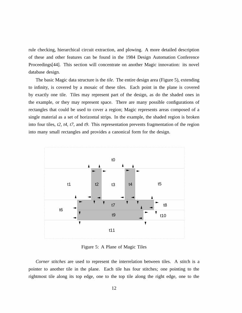
rule checking, hierarchical circuit extraction, and plowing. A more detailed description
of these and other features can be found in the 1984 Design Automation Conference
Proceedings[44]. This section will concentrate on another Magic innovation: its novel
database design.
The basic Magic data structure is thetile. The entire design area (Figure 5), extending
to infinity, is covered by a mosaic of these tiles. Each point in the plane is covered
by exactly one tile. Tiles may represent part of the design, as do the shaded ones in
the example, or they may represent space. There are many possible configurations of
rectangles that could be used to cover a region; Magic represents areas composed of a
single material as a set of horizontal strips. In the example, the shaded region is broken
into four tiles,t2, t4, t7, andt9. This representation prevents fragmentation of the region
into many small rectangles and provides a canonical form for the design.
t0
t1 t2 t3 t4 t5
t6t7 t8
t9 t10
t11
Figure 5: A Plane of Magic Tiles
Corner stitchesare used to represent the interrelation between tiles. A stitch is a
pointer to another tile in the plane. Each tile has four stitches; one pointing to the
rightmost tile along its top edge, one to the top tile along the right edge, one to the
12

bottom tile along the left edge, and one to the leftmost tile along the bottom edge.
Each tile’s corner stitches and the neighbors to which they point are shown as arrows
in the example. These four stitches make local searching very fast. For example, all
the neighbors of a given tile can be found by following stitches; in the figure, the top
neighbors of tilet7 can be found by first following its right top pointer, then by following
the bottom left pointers of the neighbors until the right edge of a neighbor is less than the
left edge of the original tile. Similar algorithms exist for locating a point on the plane,
searching for tiles in a given area, and visiting each tile in a region[45].
The remaining problem is developing a correspondence between the tile types of the
database and the physical mask layers of a fabrication process. This problem is technology
dependent; the designer must set up this correspondence for each fabrication technology
used. One approach would be to use a separate tile type for each possible combination of
overlapping layers, but this mapping would require an exponential number of types and
would fragment the database into many small pieces. Another possible solution would be
to use a separate tile plane for each mask layer. This solution requires fewer types (only
one per mask layer), but is still memory inefficient because there are many more space
tiles. This arrangement also lessens the advantages of corner stitching. Many layout
operations involve more than one layer; calculating the interactions between such tiles is
more difficult when they do not lie in the same plane.
Most technology mappings adopt an approach somewhere between the two described
above. All layers that commonly interact with one another are placed in the same plane,
while layers that do not are placed in separate ones. For example, the standard MOSIS
SCMOS technology uses five planes:well, active, metal1, metal2, andoxide. As can be
guessed from their names, the well, metal1, and metal2 planes contain types representing
the wells and the two layers of metal used in the design. The oxide plane contains the
locations of cuts in the chip’s passivation layer. The active plane contains the diffusion
and polysilicon masks, plus combinations of these layers, such as transistors. These layers
are put in the same plane because they closely interact. Interactions between layers on
different planes is much rarer; for example, few operations need to know the relative
spacings of polysilicon and metal.
The remaining problem is representing mask layers that interact with types on more
13

than one of the above planes, such as contacts. This is done using special abstract tiles that
have separate copies on both planes. For example, in Figure 6, the polysilicon, contact
cut, and metal1 masks are combined to form the single abstract typepc. Duplicate copies
of thepc tiles are kept on both the active and metal1 planes. These abstract types facilitate
analysis of the layout because mask interactions need not be calculated explicitly; they
are implied by the composite type.
m1polypc
m1
poly
cut
Physical Layers Abstract Layers
pc
Figure 6: Abstract Types
A cell is thus represented as a set of planes, each composed of tiles of varying types.
Each cell can also contain subcells; interactions between these subcells present special
problems. Magic allows nearly arbitrary overlap between cells; the only limitations are
that cells must be individually design-rule correct and that overlap must not create or
destroy devices. Any tools developed for the system must operate correctly regardless
of the cell topology. Magic’s regular circuit extractor [52] is both hierarchical and in-
cremental. To handle overlap, it extracts each cell individually, then flattens areas of
cell interaction, extracts them and adjusts the connectivity and capacitance information
accordingly. Because each cell is extracted independently of its context, only a cell and
all its ancestors must be re-extracted when it is modified.
Extracting parasitic resistances in the same manner would be extremely difficult.
Because of nearly arbitrary overlap, any point in a polygon may be used as a terminal.
14
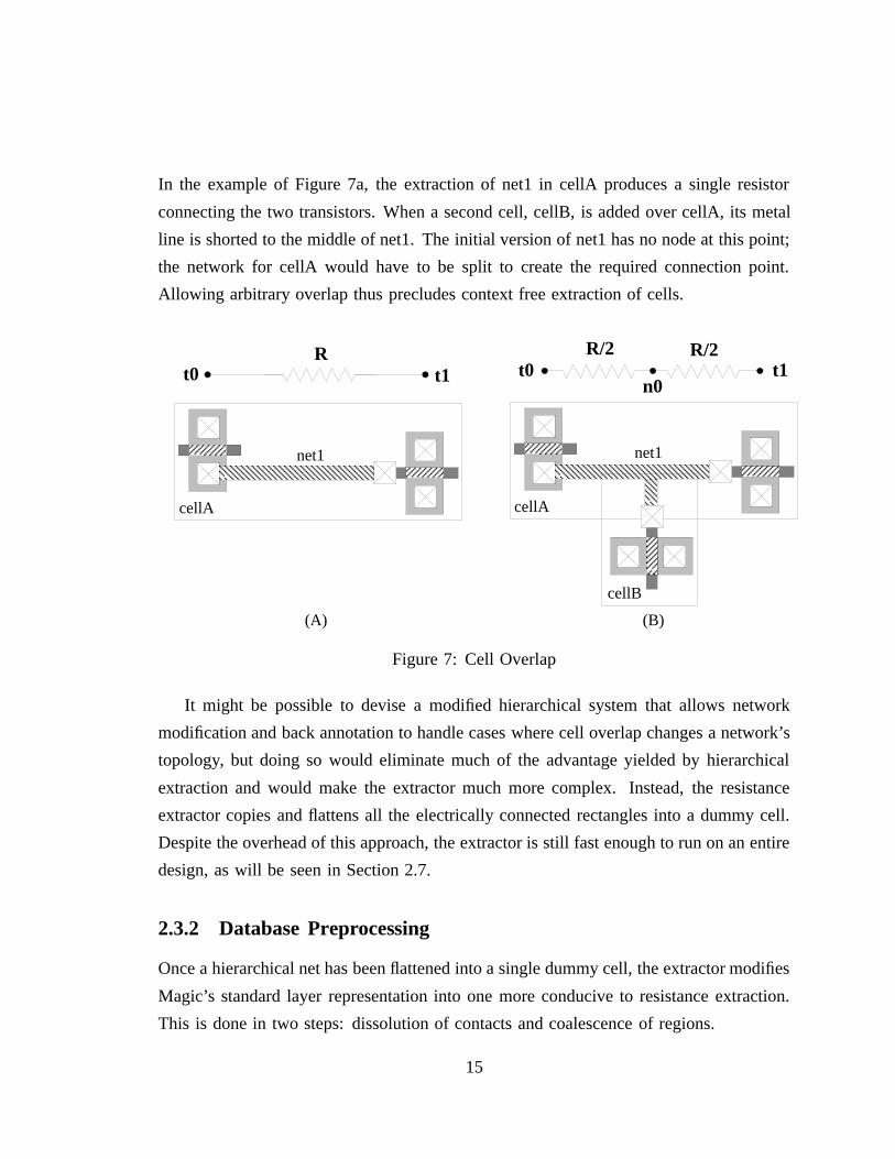
In the example of Figure 7a, the extraction of net1 in cellA produces a single resistor
connecting the two transistors. When a second cell, cellB, is added over cellA, its metal
line is shorted to the middle of net1. The initial version of net1 has no node at this point;
the network for cellA would have to be split to create the required connection point.
Allowing arbitrary overlap thus precludes context free extraction of cells.
cellA cellA
cellB
(A) (B)
net1 net1
t0R
t1 t0n0
t1R/2 R/2
Figure 7: Cell Overlap
It might be possible to devise a modified hierarchical system that allows network
modification and back annotation to handle cases where cell overlap changes a network’s
topology, but doing so would eliminate much of the advantage yielded by hierarchical
extraction and would make the extractor much more complex. Instead, the resistance
extractor copies and flattens all the electrically connected rectangles into a dummy cell.
Despite the overhead of this approach, the extractor is still fast enough to run on an entire
design, as will be seen in Section 2.7.
2.3.2 Database Preprocessing
Once a hierarchical net has been flattened into a single dummy cell, the extractor modifies
Magic’s standard layer representation into one more conducive to resistance extraction.
This is done in two steps: dissolution of contacts and coalescence of regions.
15

Contact Removal
Magic’s contact types present problems for the extractor. Resistance extraction operates
primarily on regions composed of a single mask layer. Abstract contact types tend to
fracture this single layer into multiple pieces, as shown in Figure 8a. This artificial
fragmentation makes extraction more difficult because it hides a region’s true topology.
To avoid this, the extractor notes the position of each contact and then replaces it with
its constituent mask layers (Figure 8b). This reduces the number of tiles and makes the
inherent structure of the region more explicit.
poly
poly
poly
pc poly poly
(A) (B)
Figure 8: Dissolving Contacts
Region Coalescence
Another source of artificial region fragmentation is Magic’s use of of maximum horizon-
tal strips (Figure 9a). This representation splits long horizontal regions between several
rectangles. Since the one dimensional approximation is most accurate when the con-
ducting edges of the region are perpendicular to the current flow, these areas need to be
reshaped.
A modified version of Horowitz’s fracturing algorithm [25] is used to fix them. At
each concave corner, the extractor checks to see if the width of the region measured from
16

the corner is greater than its height. If it is (Figure 9b), then each tile in the region is
split vertically at the corner. Once the tiles have been split, the extractor checks to see
if they can be combined with their vertical neighbors (Figure 9c). Corners whose region
height is greater than their width are likewise split and merged horizontally. Performing
this operation at all concave corners produces the region of merged rectangles shown in
Figure 9d.
20 λ 2 λ
(A) (B)
(C) (D)
Figure 9: Modifying Horizontal Strips
Configurations where two concave corners interact, like those in Example 10, must
be handled carefully. This configuration is not uncommon in power networks; a designer
will sometimes nick a corner out of the power bus to avoid a spacing design rule violation.
Once the region has been fractured at both corners, there are two pairs of rectangles that
share a common edge; the extractor must decide which pair to merge. In the example,
removing the horizontal edge (markedbad) leaves two tiles with current flow parallel to
their common border, while removing the vertical edge (markedgood) leaves two tiles
with current flow perpendicular to their common edge. The general rule is that the longer
of the two edges is removed; in the example, this is the vertical edge.
17

original bad goodchoices
Figure 10: Interacting Concave Corners
2.3.3 Resistance Calculation
Once the database has been preprocessed, a resistance network is formed tile by tile.
The user specifies a set of initial tile(s) that form the root of the power distribution tree,
generally the power pads, which are put into a pending tile list. Tiles are processed one
by one until none remain in the list. Each tile is processed in eight steps:
1. Check to see if this tile forms the gate or emitter of a transistor. If it does, add a
node at the center of the tile, and set the corresponding device terminal equal to it.
2. Walk along the tile’s edges looking for electrically connected materials. For each
connecting tile found, add a node at the center of the junction between tile edges.
If the other tile has not already been processed, add it to the pending list.
3. If this tile type can form the source/drain or base terminal of a device, search the
tile edges for transistor tiles. For each one found, add a node at the center of the
common edge and set the correct terminal equal to it.
4. If this tile type forms the collector of a bipolar device, search under the tile on the
emitter’s home plane for transistors. For each one found, add a node in the center
of the emitter tile and set the collector terminal equal to it.
5. Check to see if the tile originally contained any contacts. If so, add a node for
each one. If the other tiles that formed the contact have not been processed, add
them to the pending list.
18

6. Calculate the minimum and maximum X and Y coordinates of all the nodes found in
the previous steps. If max( X) min( X) > max( Y) min( Y) , assume that current
flows horizontally. If not, assume current flows vertically.
7. Sort the nodes from minimum to maximum in the direction of current flow. Merge
nodes with the same coordinate.
8. Add a resistor between each adjacent pair of rectangles.
R=
8<: RshY=width( tile) if current flow is vertical
RshX=height( tile) if current flow is horizontal
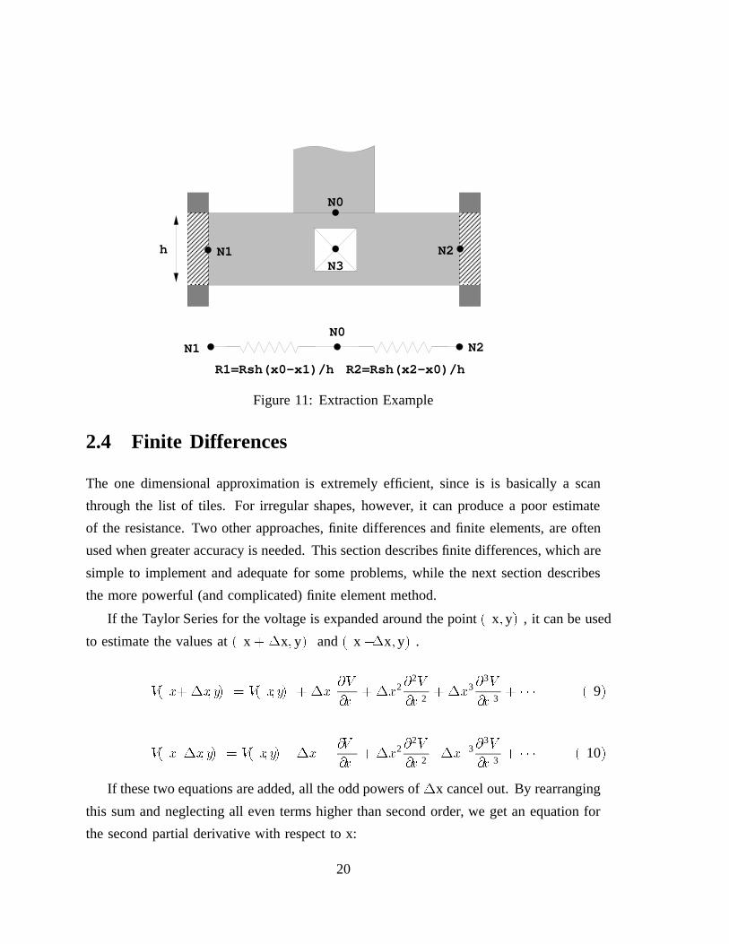
A simple example is shown in Figure 11. The extractor creates nodeN0 when it
finds the adjoining tile during the perimeter walk of Step 2. NodesN1 and N2 are
created during Step 3 because the tile forms the source terminal of two transistors. Node
N3 is created during Step 5 for the contact contained within the rectangle. Since the
greatest horizontal separation (between nodesN1 andN2) is greater than the maximum
vertical separation (between nodesN0 andN3), the extractor assumes that current flows
horizontally. The nodes are sorted by x coordinate; since NodesN0 andN3 have the
same value, they are merged. Two resistors, R1 and R2, are created between the node
pairs,N1 N 0 andN0 N 2, and are added to the overall network description. The
extractor marks this tile as processed and goes on to the next one in the pending list.
When all the tiles associated with a node have been processed, the resistors and
transistors connecting to the node are examined. Resistors with both terminals connected
to the node are eliminated. The extractor tries to combine any resistors in parallel
connecting to the node. If there are no transistors and only one resistor connected to the
node, the node and its connecting resistor are eliminated. Nodes with two connecting
resistors and no transistors are also removed, and their resistors are combined.
The extractor continues in this manner until all the tiles are visited and all the nodes
have been processed. The resulting network of nodes, resistors, and transistors is then
saved in a file for processing by the linear solver.
19
N1
N0
N3N2
N0N1 N2
R2=Rsh(x2-x0)/hR1=Rsh(x0-x1)/h
h
Figure 11: Extraction Example
2.4 Finite Differences
The one dimensional approximation is extremely efficient, since is is basically a scan
through the list of tiles. For irregular shapes, however, it can produce a poor estimate
of the resistance. Two other approaches, finite differences and finite elements, are often
used when greater accuracy is needed. This section describes finite differences, which are
simple to implement and adequate for some problems, while the next section describes
the more powerful (and complicated) finite element method.
If the Taylor Series for the voltage is expanded around the point( x; y) , it can be used
to estimate the values at( x +x; y) and( x x; y) .
V( x+x; y) = V( x; y) +x@V
@x+x2@
2V
@x 2+x3@
3V
@x 3+ ( 9)
V( xx; y) = V( x; y) x @V
@x+x2@
2V
@x 2x 3@
3V
@x 3+ ( 10)
If these two equations are added, all the odd powers ofx cancel out. By rearranging
this sum and neglecting all even terms higher than second order, we get an equation for
the second partial derivative with respect to x:
20

@2V
@x 2 V( x+x; y) + V( xx; y) 2V( x; y)
x2( 11)
An analogous equation for@2V=@y 2 can be derived in the same way. When these
two equations are added, the result is an approximation for Laplace’s equation in two
dimensions:
@2V
@x 2+@2V
@y 2 V( x+x; y) + V( xx; y) 2V( x; y)
x2+
V( x; y+y) + V( x; yy) 2V( x; y)y2
= 0 (12)
Rearranging Equation 12 gives an approximation for V( x; y) in terms of its four
neighbors, V( xx; y) ,V( x +x; y) , V( x; yy) , and V( x; y +y) .
V( x; y) y2( V( x+x; y) + V( xx; y) )
2x2 + 2y2+x2( V( x; y+y) + V( x; yy) )
2x2 + 2y2
( 13)
If the region is covered with a rectilinear mesh, as shown in Figure 12, then the
voltage distribution can be calculated by solving the system of linear equations relating
the mesh node potentials to one another. In this derivation, the distances between mesh
points in a given direction (x andy are constants), but an equivalent expression for
a nonuniform node distribution may be derived in the same manner; the only difference
is that Equation 10 must be scaled by the ratio of the mesh spacings so that the first
derivative terms will still cancel one another[22].
While Equation 13 is clearly true for points in the interior of the mesh, it must be
modified for points along the boundary. For points on a conducting edge, the potential
is fixed atVc, the edge’s potential. For points along an insulating edge, the boundary
condition requires than the normal current be 0. This can be achieved by mirroring the
voltage about the edge:
V( x; y) = 2y2V (x+x;y)+x 2( V( x; y+y) +V( x; yy) )
2x2+2y2leftedge ( 14)
21

Figure 12: Finite Difference Mesh
V( x; y) = 2y2V( xx; y) +x2( V( x; y+y) +V( x; yy) )
2x2+2y2rightedge ( 15)
V( x; y) = y2( V( x+x; y) +V( xx; y) ) +2x2V( x; y+y)
2x2+2y2bottomedge ( 16)
V( x; y) = y2( V( x+x; y) +V( xx; y) ) +2x2V( x; yy)
2x2+2y2topedge ( 17)
For convex corners, the voltage is mirrored in both directions.
These equations give the potential for discrete points in the region; the next step is to
convert this system of equations into a corresponding resistance network. Surprisingly, a
resistance network can be produced without explicitly calculating all the voltages interior
to the region. The next two sections describe an efficient method for performing the
conversion: the finite difference grid is represented as a mesh of resistors, which can be
transformed directly into the desired resistor network.
2.4.1 Physical Analogs of Finite Differences
Just as the discrete finite difference equation was formulated to approximate to the con-
tinuous Laplace Equation, a discrete resistor network can be formulated to approximate
the continuous resistive region. Consider the resistor network of Figure 13. Applying
Kirchoff’s Current Law at node V( x; y) gives:
22

Gx
Gx
Gy
Gy
V(x+1,y)
V(x,y+1)
V(x-1,y)
V(x,y-1)
V(x,y)
Figure 13: Lumped Analog of Finite Difference Equations
V( x; y) =GXV( x+x; y) +G XV( xx; y) +G Y V( x; y+y) +G Y V( x; yy)
2GX + 2GY
( 18)
This equation is very similar to Equation 13; if Gx y2 and Gy x 2, then the
two are identical. The solution is not unique, however; any values of Gx and Gy that have
the same ratio Gy=G x = x2=y 2 will produce the same voltage distribution. With this
in mind, we can pick conductance values that also produce the correct current distribution.
Equations 19 and 20 give the discrete approximations for the current density.
Jx = E x V( x+x; y) V( x; y)x
( 19)
Jy = E x V( x; y+y) V( x; y)y
( 20)
If x andy are small, then Jx and Jy will be essentially constant across the rectangle
and the integral of Equation 2 will just be the current density times the cross-sectional
area. For a region of thicknesst:
Ix t( y) Jx = ty
x( V( x+x; y) V( x; y) ) ( 21)
Gx = ty
x( 22)
23

Iy t( x) Jy =tx
y( V( x; y+y) V( x; y) ) ( 23)
Gy = tx
y( 24)
The values ofGx andGy have the correct ratio,x2=y 2. These analogs provide
an intuitive feeling understanding of finite difference analysis. A region is broken into a
set of small rectangles, each of which is replaced by a simplified resistor network. This
network can then be solved and replaced by an equivalent network that does not contain
the interior portion of the mesh.
2.4.2 Solving the Equations
Once the equations have been formulated and modified to account for the various bound-
ary conditions, the resulting system must be solved. Any algorithm for solving sparse,
positive definite matrices may be used here, including Successive Overrelaxation (Section
5.5.2) and Cholesky Decomposition (Section 5.5.1), but significant performance advan-
tages can be obtained by using the node elimination approach of Harbour and Drake[22].
As noted in the previous section, a finite difference formulation produces a mesh of
lumped resistors, as does the entire extractor; instead of applying a test voltage to each
boundary in succession, node elimination simply transforms the finite difference network
into the desired network. To do this, the conductance matrix is first partitioned into two
sections: one containing the set of nodese that are to be retained and the other the set
of nodesi that are to be removed.
G=
24 Gee Gei
Gi e Gi i
3524 Ve
Vi
35 =
24 Ie
Ii
35 ( 25)
Since there is no current injected into the internal nodes,Ii = 0, and the equations
can be rewritten and solved forVe:
GeeVe +GeiVi = Ie ( 26)
Gi eVe +Gi iVi = 0 ( 27)
24

Rearranging Equation 27 and substituting it into 26 gives an equation forVe alone:
Vi = G 1i i Gi eVe ( 28)
( Gee G eiG1i i Gi e) Ve = Ie ( 29)
The term in parenthesis in Equation 29 is an equivalent conductance matrix G0
ee that
relates the boundary nodes and voltages without calculating the internal values; it is the
same matrix that would be produced by applying a test voltage to each edge in turn and
measuring the currents flowing to all the other edges. The conductance matrix for the
entire system could be constructed using this equation, but invertingGi i would be very
expensive because it is nearly as large asG. Instead, Equation 29 can be applied to
individual nodes as they are created.
G1
G2
G3
G4
N1
N2
N3
N4
N1
N2
N3
N4
G1G2/GT
G2G3/GTG3G4/GT
G1G4/GT
G1G3/GT
G2G4/GT
GT=G1+G2+G3+G4
N0
(A) (B)
Figure 14: Node Elimination
Consider a nodeN0 that connects ton other nodes, shown in Figure 14a forn = 4.
This node can be eliminated by applying Equation 29. The inverse matrix G1ii is the
inverse of the sum of all the conductors connecting to the node, and Gei and Gie are just
25
the row and column vectors containing the values of G1 Gn. Multiplying these terms
gives the value for a new resistor Gij in terms of the old ones.
Gij( n e w) = Gij( old ) +G0iG0j
GT
( 30)
GT =nX
k=1
Gk ( 31)
Once all the resistor analog elements connecting to an internal point have been cal-
culated, this formula can be applied to eliminate the node. Internal nodes can thus be
eliminated as they are created; if the order in which nodes are processed is chosen care-
fully, this algorithm will be considerably faster and will use less memory than would
creating the entire matrix and then solving it. Section 2.6 describes an implementation
of this algorithm.
2.5 Finite Elements
The finite difference approximation is adequate for regions without much variation in
width and current density. When the current density does change considerably, main-
taining acceptable accuracy is difficult due to the rectilinear grid; using small enough
elements to provide sufficient accuracy in complicated areas requires use of too many
elements in simpler sections. Since power supply networks often contain large variations
in width and current density, solving them using finite differences would be very expen-
sive. A more general approach, the finite element method, can be used to circumvent
this problem.
A two dimensional voltage distribution forms a 3-dimensional surface. The finite
element method approximates this curved surface as a set of triangular patches called
elements; the voltage in each element is a linear interpolation of the voltages at the ver-
tices. Since the interpolation is linear, the gradient of the potential is constant throughout
the patch, and the divergence of the gradient is zero. A constant gradient makes the
current density constant, and zero divergence makes Laplace’s equation valid inside each
element.
26

x
y
V
Original surface
x
y
V
Finite Element Approximation
Figure 15: Approximation of a Potential Surface
Since the potential in each element is fixed by the potentials at its vertices, the key
is finding a set of equations that relate an element’s vertex potentials to one another and
to those of neighboring elements. This is done by requiring the current flow between
elements to be continuous; the current flowing out across each edge of one element must
equal that flowing in across the same edge of its neighbor. For the center element in
Example 16, this gives three equations:
nc
na
nbJ1
J2J3
Figure 16: Matching Current Flow Across Boundaries
27

J1 na = 0
J1 nb = J3 nbJ1 nc = J2 nc
By repeating this for all the patches adjoining a given vertex, the finite element
approximation produces an equation defining the vertex’s potential in terms the values at
adjoining vertices. When all the elements covering the region are processed, the result is
a system relating the node potentials to one another; with the correct potentials applied
at the conducting boundaries, the system will give an approximate solution to Laplace’s
equation for the region. The accuracy will depend on how closely each patch lies to
the actual surface. As patches get smaller, the surface regions they represent become
more planar, and the solution accuracy improves. The same conclusion can be reached
by considering the current densities; as patches get smaller, the current density of the
surface region that they represent becomes more and more constant and approaches that
of the patch. This suggests that the ideal mesh would have many small elements in places
where the current density changes rapidly, and fewer, larger ones where the density is
more uniform. Section 2.6 explores this problem in detail.
The finite element method can also be considered a generalization of the finite differ-
ence method. The finite difference approximation requires that the first derivatives of the
potential be continuous in both the X and Y directions. Using finite elements, the first
derivative (in this case the gradient) must again be continuous, but the mesh does not
have to be rectilinear and the derivative need not be independently continuous in both
the X and Y directions.
Like the finite difference method, relations between the vertex node potentials are
often expressed in terms of a physically analogous resistor network to allow use of the
node elimination technique described in the last section. Appendix A contains a detailed
derivation of the analog for a triangular finite element; only the result is included here.
The relation between the three vertices is represented as three conductors, with values
given below.A is the element’s area. A network for the entire system can be constructed
by calculating the conductances for each patch and adding together the two elements that
28

adjoin each edge.
i
j
k
(xi,yi)
(xj,yj)
(xk,yk)
i
k
j
G1
G2
G3
Figure 17: Triangular Finite Element
G1 =
4A( xjxk + xixk x 2
k x ixj + yjyk + yiyk y 2k y iyj) (32)
G2 =
4A( xixj + xjxk x 2
j x ixk + yiyj + yjyk y 2j y iyk)
G3 =
4A( xixj + xixk x 2
i x jxk + yiyj + yiyk y 2i y jyk)
2.5.1 Rectangular Elements
Another commonly used element shape is the rectangle. The discrete conductors for a
rectangular element (Figure 18) can be derived by considering it as two triangles. Solving
the two elementsi jk and i j0k and summing the two diagonal resistors gives values for
the five conductors.
Gj = ( ( y1 y 0) ) = ( 2( x1 x 0) )
Gk = ( ( y1 y 0) ) = ( 2( x1 x 0) )
Gl = ( ( x1 x 0) ) = ( 2( y1 y 0) )
Gm = ( ( x1 x 0) ) = ( 2( y1 y 0) )
Gn = 0
( 33)
29

i j
kj’
Gn
Gj
Gk
Gl Gm
(X0,Y0)
(X1,Y1)
(X1,Y0)
(X0,Y1)
Figure 18: Rectangular Finite Element
As expected, these equations are similar to those of the finite difference analog in
Section 2.4.1; the total conductance is the same, but in the finite element case, it is split
between the two node-pairs along each edge instead of being assigned to a single one.
For a uniform grid, each finite element node-pair not on a boundary will receive half an
element of conductance, making the finite element and finite difference physical analogs
identical. Finite difference analysis is thus a special case of finite element analysis with
rectilinear elements.
2.5.2 Boundary Conditions
Satisfying the boundary conditions for finite element systems is simple. Insulating bound-
aries conceptually can be treated as any other region, except that the conductance is 0.
Because of this, the discrete conductors all have 0 value and can be ignored. Perfectly
conducting boundaries are regions for which =1, so the discrete conductors have in-
finite value; all nodes adjoining such an element are shorted together and are represented
by a single node in the system matrix.
30

2.6 Finite Element Implementation
To check the accuracy of the simple one-dimensional extractor, Ariel also includes a finite
element extractor. Since finite element analysis is slow, this second extractor will only
perform it on subregions too complicated to extract by other means. Techniques described
in the next two sections subdivide a region and identify the parts where detailed analysis
is either unnecessary or redundant. These methods are based on similar components
of the extractor EXCL[35]. Following this is a description of the finite element mesh
generation and solution techniques used.
2.6.1 Region Subdivision
Finite difference and finite element analysis both produce resistors between each pair of
nodes in a net, or( N2 N) = 2 elements in all. For a power bus, the number of nodes
is quite large because the region itself is large and has many connecting transistors.
Producing a network for the entire region at once is not feasible; it would take too long
to compute and would be too large to use. The region needs to be subdivided into smaller
sections which can be extracted independently of one another.
The best way to do this is using the idea ofbreaklinesdeveloped by Horowitz [25]
and extended by McCormick [35]. Breaklines are subdivisions added in long, straight
parts of the region in such a way that the current distribution is not significantly dis-
turbed. An example is shown in Figure 19. At the region’s corner, the lines of constant
potential are unevenly spaced, but they become quite uniform a relatively short distance
away. If the region is split parallel to these field lines, and the newly created regions
are modelled as perfectly conducting boundaries, then the region’s field is virtually un-
changed. McCormick calculated that splitting the region one square away from a source
of disturbance only adds an error of about 0.1% in the calculated resistance.
Although adding a breakline increases the total number of nodes by 2, it makes two
smaller problems out of the original large one. When breaklines are added next to all
long, straight sections, the large region is divided into many small ones.
Implementing this algorithm in a corner stitched database is straightforward. Once
the region coalescence of Section 2.3.2 has been performed, the extractor makes a second
31

Figure 19: Adding Breaklines to Regions
(A) (B) (C)
Figure 20: Implementing Region Subdivision
pass through the database looking for rectangles with an aspect ratio greater than 2 or
less than 1/2, like the one shaded in the example of Figure 20a. Each of these rectangles
is copied into a dummy cell. The four edges of the original rectangle are checked
for adjoining material; each adjoining rectangle found is bloated by its width, and any
material in the copied rectangle is erased, leaving the truncated rectangle shown shaded
in Figure 20b. An analogous operation is performed for any contacts that overlap the
rectangle; they are bloated by the height of the original rectangle, then erased in the copy.
In the example, this leaves two shaded regions (Figure 20c), which represent areas where
the current flow and potential are uniform. The rectangle is split into parts along the left
and right edges of the shaded regions. The new rectangles corresponding to the shaded
parts of the original are marked as having uniform current flow.
32

A B C D
E F G H
Figure 21: Possible Rotations of a Region
2.6.2 Subregion Library
The extra region fracturing performed in the previous section produced two classes of
rectangles: those with uniform current flow and those with nonuniform flow. For the
former, resistance calculation is trivial; from Section 2.2, R= RshL= W. The latter require
further calculation. The resistance for each nonuniform rectangle cannot be calculated
by itself; it must be considered along with its neighbors. Each group of adjoining non-
uniform tiles form acluster, which is bounded by space tiles, modelled as insulating
edges, and by transistors, contacts, and uniform-flow rectangles, which are modelled as
perfectly conducting edges.
Due to the repetitive nature of VLSI designs, many of these clusters are either identical
or mirrored/flipped copies of one another. Each such group need only be extracted once.
This is done using a dynamic library. Before a cluster is extracted, the relative positions
of its constituent rectangles and conducting edges are used as the key to a hash table.
The entry corresponding to each key is the resistance network extracted for the cluster. If
an entry is found for a given cluster configuration, then a copy of the entry is appended
to the resistor network. If no entry is found, then a new one is added for the cluster after
it is extracted.
33

R=2.559*Rsh R=2.559*Rsh
Figure 22: Region Scale Invariance
Since cells are often rotated or flipped, it is important that the clusters match regardless
of rotation. Figure 21 shows the 8 possible rotations of an asymmetric cluster. There
are a number of ways to make entries match regardless of rotation. One approach would
be to make an additional key for each unique rotation of the cluster. The advantage of
this is that table accesses are fast; no additional processing must be done to a cluster
before it is compared against the library keys. The primary disadvantage is that it uses
additional memory; since the key for an entry is often as large as the entry itself, and
most large clusters are asymmetric, such a library would be prohibitively large. Instead,
a single canonical key is used. The extractor first calculates the centroid of each region,
then rotates the region so that the center of gravity is as low and as far to the left as
possible. In the example, rotation F would be chosen. This scheme usually only requires
one key, making it memory efficient. It has two disadvantages: the library access time is
greater due to the cost of calculating the centroid, and the rotation may not be unique if
the centroid lies on the line x= y. In practice, the increased access time is unimportant
because extraction time is dominated by the finite element calculation itself. To ameliorate
the second problem, the extractor calculates the centroid of the conducting edges if the
correct rotation is ambiguous. (Since the edges are actually lines, they are first assigned
a small finite width.) Sometimes, this will also fail to give a unique rotation. In this
case, the region will actually get extracted more than once. The loss of efficiency due
to unnecessary duplication of extraction is negligible, however; in practice, the large
clusters whose processing dominates the extraction time have too many rectangles and
edges to be ambiguous.
One other possible enhancement is scale invariance. Although they are of different
34

sizes, the two regions of Figure 22 have the same resistance. In his library implementa-
tion, McCormick normalizes all rectangles to 1/256th of the first rectangle’s height. Such
an implementation would not work for a power bus extractor due to the great variation
in width. It is not uncommon for minimum width wires to connect to an extremely
wide main power bus. Any rounding in the width of these minimum width wires due to
quantization could introduce substantial error in the overall resistance.
Another scaling implementation might be possible, but its utility in the power network
domain is questionable. The large, multirectangle regions that dominate the extraction
time are not scaled versions of other regions, and any time spent providing scale inde-
pendence is wasted for them. Since the potential return for scaling is problematical, the
extractor does not use it.
2.6.3 Mesh Generation
The extractor must produce a network for any cluster that does not match an entry in the
library. McCormick and Horowitz both use finite difference analysis when they need to
accurately extract a region; unfortunately, this approach proves inadequate for power bus
extraction. Power buses have a wide variations in width; a rectilinear grid that provides
adequate accuracy near small features will run too slowly in the large, coarse sections of
the design.
To accommodate large feature size variation, some sort of nonuniform finite element
mesh generation is needed. One possible approach is the adaptive mesh generation
algorithm devised by Machek and Selberherr[34]. This method has two drawbacks for
resistance extraction. First, it requires that the internal node voltages be calculated; the
fastest solution algorithm for resistive meshes, node elimination (Section 2.4.2), does not
calculate these intermediate values. Use of adaptive mesh generation would require the
one of the slower solution techniques be used. The other problem is that the mesh would
have to be regenerated for each edge; since the potential distribution varies depending
on the boundary to which the voltage is applied, the mesh will also vary.
Because of these drawbacks, a modified version of Kemp’s heuristic mesh generation
35

1
4
2
5
3
A
E
C D
B
F
Figure 23: Sources of Potential Disturbance
[31] is instead used. The basic idea of this algorithm is to produce a mesh with many el-
ements in places where the current density is changing rapidly and fewer in places where
it is changing slowly. To do this, the region is first represented as a set of rectangular
elements1 containing regions of homogeneous resistivity. Each of these elements adjoin-
ing a point of voltage disturbance needs to be subdivided. The disturbances are caused
by concave corners in the regions. In the example of Figure 23, the disturbances are the
bend in the region (labelled 1) and the corners around the contact (labelled 2-5). Kemp
also uses the entire edge between two regions of differing resistivity (labelled A-F), but
this seems unnecessary; as can be seen from the potential lines, the current does not
change rapidly except at the corners.
Each element adjoining a disturbance is recursively split in two until the elements
nearest the corner are below some minimum size. The basic idea in splitting is to
subdivide the element in such a way that the resulting children are well ratioed,2 and to
1The initial elements are rectangles because Magic’s database only supports orthogonal shapes. Al-though Kemp’s algorithm can handle arbitrary shapes, the current discussion is limited to the Manhattancase.
2The aspect ratio of an element is the length of the short side divided by the length of the long one;
36

(a) (b) (c) (d) (e)
Figure 24: Subdivision of Elements
minimize the number of nodes required by making the split points of adjacent elements
align. The following rules (illustrated in Figure 24) are applied:
Ill-ratioed rectangles are split in two along their long side.
a. If there is an edge between two elements along one side, and
subdividing there does not give children more ill-ratioed than the parent,
split the element at the edge. If there is more than one such edge, use
the one that gives the best ratioed children.
b. If there is no such edge, split the element in the middle.
Well-ratioed rectangles can be split in either direction.
c. Split at the adjacent edge that gives the best ratioed children.
d. If no such edges exist, split along a line perpendicular to the
expected direction of current flow.
e. For a corner element with no adjacent edges, split in both
directions.
Once the adjacent element is subdivided, the same procedure is applied to all of its
children that are next to the disturbance. This continues until all of the adjacent elements
are smaller than some predefined size. Figure 25 shows how this algorithm operates on
a concave corner. The edges are numbered in the order in which they were added, with
the letter (a-e) in parentheses showing which rule was applied.
the closer this ratio is to 1, the more ’well-ratioed’ the element is.
37
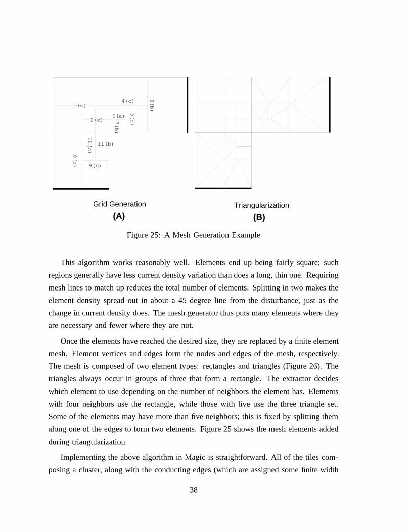
TriangularizationGrid Generation
1(e)
2(e)
3(b)
4(c)
5(d)
6(a)
7(b)
8(c) 9(b)
10(c)
11(b)
(A) (B)
Figure 25: A Mesh Generation Example
This algorithm works reasonably well. Elements end up being fairly square; such
regions generally have less current density variation than does a long, thin one. Requiring
mesh lines to match up reduces the total number of elements. Splitting in two makes the
element density spread out in about a 45 degree line from the disturbance, just as the
change in current density does. The mesh generator thus puts many elements where they
are necessary and fewer where they are not.
Once the elements have reached the desired size, they are replaced by a finite element
mesh. Element vertices and edges form the nodes and edges of the mesh, respectively.
The mesh is composed of two element types: rectangles and triangles (Figure 26). The
triangles always occur in groups of three that form a rectangle. The extractor decides
which element to use depending on the number of neighbors the element has. Elements
with four neighbors use the rectangle, while those with five use the three triangle set.
Some of the elements may have more than five neighbors; this is fixed by splitting them
along one of the edges to form two elements. Figure 25 shows the mesh elements added
during triangularization.
Implementing the above algorithm in Magic is straightforward. All of the tiles com-
posing a cluster, along with the conducting edges (which are assigned some finite width
38

Rectangular Triangular
Figure 26: Finite Elements Used in Generation
so that they can be represented as a tile) are copied into a dummy cell. Solution accuracy
can be controlled using an optional scale factor by which all rectangles are magnified as
they are copied. A large scale factor results in smaller final elements near a disturbance.
The cluster is then searched for concave corners. At each such corner, the horizontal tile
is split along the y-axis at the corner to produce the three initial rectangles of Figure 25,
each of which is then processed by the above algorithm. The algorithm is done when
the corner’s adjacent elements are all 1 by 1 squares. The extractor then makes a second
pass through the entire cluster, looking for elements with more than five neighbors. Each
such element is subdivided again, and the adjacent elements are rechecked to insure that
the additional edge does not leave them with too many neighbors. The final triangular-
ization is not explicitly performed because Magic can only represent rectangles. Instead,
the extractor adds the elements for all three triangles at once whenever a five-neighbor
rectangle is encountered.
2.6.4 System Solution
Once the mesh has been generated, it must be solved for the node to node resistances.
The extractor uses Harbour and Drake’s node elimination algorithm (Section 2.4.2) to
remove the unwanted interior nodes. In implementing this algorithm, the extractor has to
decide the order in which the internal nodes will be processed. If the mesh is rectilinear,
as Harbour and Drake’s is, then one good ordering is to process the nodes row by row.
The extractor walks down the long side of a rectangle, adding rows of new nodes. As the
mesh is extended for each element in a row, any nodes sandwiched between this element
and previously processed ones have all their connections in place and may be eliminated.
39
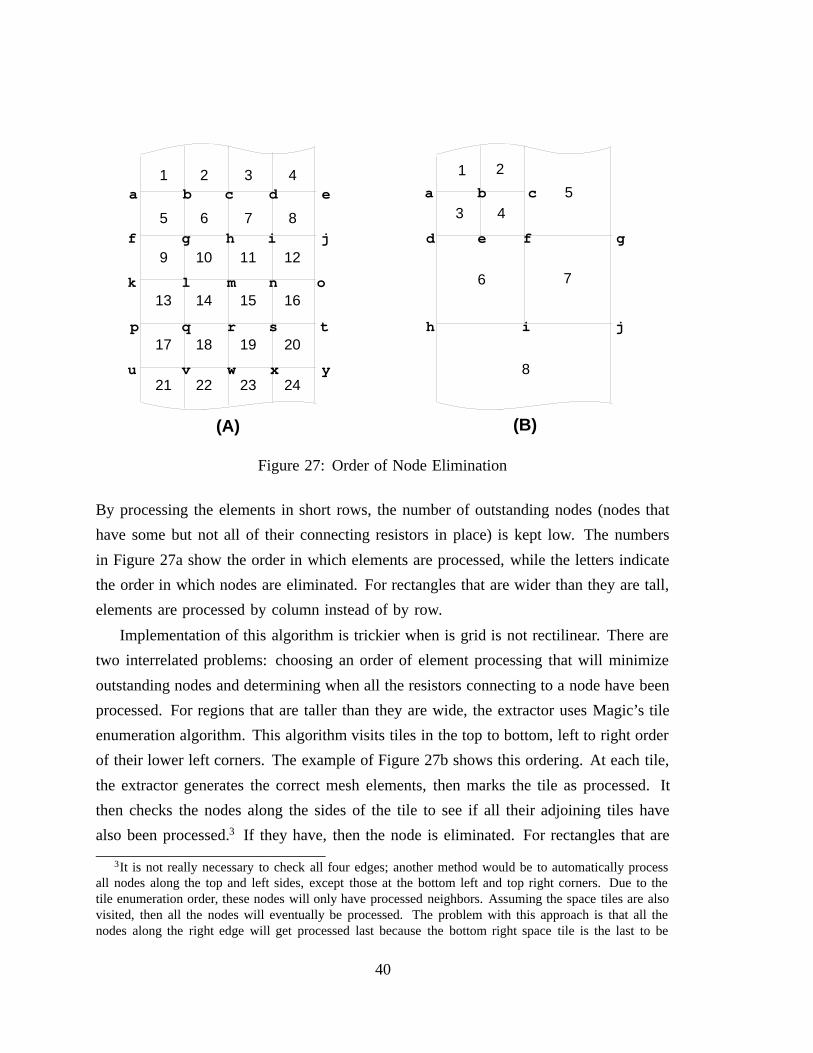
1 2 3 4
5 6 7 8
9 10 11 12
13 14 15 16
17 18 19 20
21 22 23 24
a b c d e
f g h i j
k l m n o
p q r s t
u v w x y
a b c
d e f g
h i j
1 2
3 45
6 7
8
(A) (B)
Figure 27: Order of Node Elimination
By processing the elements in short rows, the number of outstanding nodes (nodes that
have some but not all of their connecting resistors in place) is kept low. The numbers
in Figure 27a show the order in which elements are processed, while the letters indicate
the order in which nodes are eliminated. For rectangles that are wider than they are tall,
elements are processed by column instead of by row.
Implementation of this algorithm is trickier when is grid is not rectilinear. There are
two interrelated problems: choosing an order of element processing that will minimize
outstanding nodes and determining when all the resistors connecting to a node have been
processed. For regions that are taller than they are wide, the extractor uses Magic’s tile
enumeration algorithm. This algorithm visits tiles in the top to bottom, left to right order
of their lower left corners. The example of Figure 27b shows this ordering. At each tile,
the extractor generates the correct mesh elements, then marks the tile as processed. It
then checks the nodes along the sides of the tile to see if all their adjoining tiles have
also been processed.3 If they have, then the node is eliminated. For rectangles that are
3It is not really necessary to check all four edges; another method would be to automatically processall nodes along the top and left sides, except those at the bottom left and top right corners. Due to thetile enumeration order, these nodes will only have processed neighbors. Assuming the space tiles are alsovisited, then all the nodes will eventually be processed. The problem with this approach is that all thenodes along the right edge will get processed last because the bottom right space tile is the last to be
40

wider than they are tall, the tiles are instead visited left to right, top to bottom.
This enumeration works fairly well for regions that have an aspect ratio that is not
near one, but is not as useful for more complex areas that are more or less square. A
better algorithm might try and follow the twists and turns of individual rectangles within
the cluster. For complicated structures, however, doing this while still ensuring that all
elements are visited is tricky. For simplicity, the straightforward enumeration is used
even for more complicated structures.
2.7 Results
To compare the speed and accuracy of the two algorithms, I extracted the ground buses
from two midsized circuits: the register file from the MIPS-X microprocessor[24], and
a self-timed divider[60]. Table 2 gives the circuit sizes and running times on a Titan,
a 15-MIP RISC machine. The finite element grid size chosen gave solutions accurate
to about 2%[35]. Even with the library of stored shapes, subdivision of regions, and
heterogenous grid, the finite element extractor is over two orders of magnitude slower
than the simple polygon extractor.
Size Running Time (seconds)Polygonal Finite
Circuit Transistors Rectangles Decomposition Element
Register 10159 12918 68 13245FileSelf-Timed 5777 7173 39 10393Divider
Table 2: Extraction Times for Example Circuits
The summary of library effectiveness in Table 3 suggests why the finite element
method is so much slower. The first two columns show the number of shapes that missed
and matched in the library. The third column gives the time required to solve the shapes
visited. These extra outstanding nodes add overhead to the node elimination. It is therefore faster, thoughless elegant, to check all the edges.
41

which were not present, while the final column gives the time that would have been
required to solve all the matching shapes had the library not been used. Although over
90% of the shapes matched for both test cases, the time saved by using the library was
relatively small: less than 30% for both cases. This suggests that the finite element solver
is spending most of its time on a few large, complicated shapes that occur only once in
each design. In retrospect, this is not particularly surprising. A power bus is generally
fairly wide near its root; this extra width limits the number of places where long, straight
sections free of current disturbances can be found. Each bus will thus have at least one
large region with multiple connection points that will need to be solved. Conversely, the
shapes that match will be the simple bends and junctions near the leaves of the network,
and the time saved by each match will be small.
Miss MatchMiss Match Solve Saved
Circuit Count Count Time Time
Self-Timed 260 3535 10337 3085DividerRegister 154 4195 13150 5164File
Table 3: Previous Solution Library Efficacy
Despite the disparity in running times, the two extractors produce nearly identical
results. Figure 28 shows the accuracy of the methods on the two test circuits. For each
circuit, I applied the same input current distribution to both networks and compared the
resulting voltages for nodes in the metal sections of the bus. The correlation between the
methods is fairly good in both cases.
To see how the simple polygon extractor performed on larger designs, I extracted
power networks for the three large CMOS designs described in Section 1.2. The results
are given in Table 4. In all cases, the extraction time was dominated by flattening the
power network layout; the remaining preprocessing steps and the actual extraction were
less than half the total. This implies that substantial speed improvements will be difficult
unless the design methodology restricts cell overlaps sufficiently to permit hierarchical
42

MIPS-X Register File
0 0.06Finite Element Method (Volts)
00.
06P
olyg
onal
Dec
ompo
sitio
n M
etho
d (V
olts
)
Self-Timed Divider
0 0.125Finite Element Method (Volts)
00.
125
Pol
ygon
al D
ecom
posi
tion
Met
hod
(Vol
ts)
Figure 28: Accuracy of Resistance Extraction
extraction. Despite the cost of flattening the bus, however, the extractions still generally
took ten minutes or less. Since the polygonal extractor gives nearly the same result in
a fraction of the time required by the finite element method, I chose it as my primary
extractor for large designs.
Time (seconds) MemoryCircuit Flattening Fracturing Extraction Total Usage (Mb)
MIPS-X Ground 418 54 139 611 50.3MIPS-X Vdd 299 39 50 388 57.0SPIM Ground 244 56 78 378 27.3SPIM Vdd 289 53 118 460 33.9 Titan Ground 238 35 115 388 43.6 Titan Vdd 413 79 130 622 66.8
Table 4: Example Circuit Extraction Times
The rightmost column in the table gives the memory usage for the various designs.
The memory usage is fairly large, primarily due to flattening the power bus. Extraction
43

without flattening is not an easy problem, however. Section 2.3 described why hierarchical
extraction is difficult when arbitrary overlaps are permitted: overlapping sections of layout
may connect to one another at any location. Flattening one section of the layout at a time,
which Magic’s capacitance extractor does for regions of cell overlap, would also be tricky
to implement for resistance extraction. A tile’s resistance cannot be easily calculated if
it has been bisected by the section boundary, and determining which tiles are part of the
power bus is also difficult. There is no obvious approach that I can see for reducing the
extractor’s memory usage; this is one of the areas in which I plan future work.
44
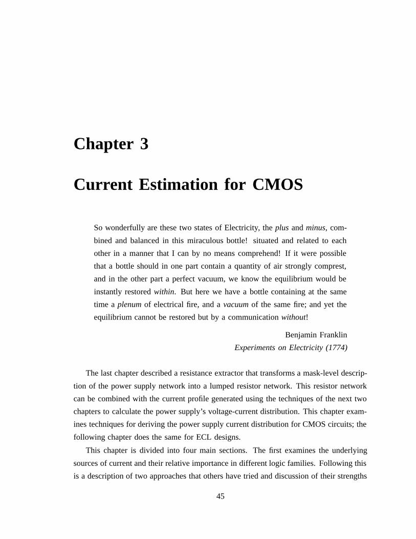
Chapter 3
Current Estimation for CMOS
So wonderfully are these two states of Electricity, theplus andminus, com-
bined and balanced in this miraculous bottle! situated and related to each
other in a manner that I can by no means comprehend! If it were possible
that a bottle should in one part contain a quantity of air strongly comprest,
and in the other part a perfect vacuum, we know the equilibrium would be
instantly restoredwithin. But here we have a bottle containing at the same
time aplenumof electrical fire, and avacuumof the same fire; and yet the
equilibrium cannot be restored but by a communicationwithout!
Benjamin Franklin
Experiments on Electricity (1774)
The last chapter described a resistance extractor that transforms a mask-level descrip-
tion of the power supply network into a lumped resistor network. This resistor network
can be combined with the current profile generated using the techniques of the next two
chapters to calculate the power supply’s voltage-current distribution. This chapter exam-
ines techniques for deriving the power supply current distribution for CMOS circuits; the
following chapter does the same for ECL designs.
This chapter is divided into four main sections. The first examines the underlying
sources of current and their relative importance in different logic families. Following this
is a description of two approaches that others have tried and discussion of their strengths
45
and weaknesses. Next is a description of the switch level simulation approach that I
have adopted, together with analysis of some of the more subtle problems that had to be
solved. The final section discusses the estimator’s performance on some real designs.
3.1 Introduction
The currents that circuits draw from their power supply buses can be divided into two
categories:capacitiveandshort-circuit. The CMOS inverter in Figure 29 dissipates both
currents. When the inverter inputIn falls, Transistor M1 turns on and begins to charge
the capacitor at NodeOut. This charging requires the capacitive current component Icap.
M1
M2
OutIn Isc
Icap
Icap
Isc
Cur
rent
time
In
Out
Vol
tage
time
Figure 29: Simple Current Example
As M1 is turning on, the n-channel transistor M2 is turning off. WhileIn is in
the rangeVTN < VI < Vdd V TP , both transistors are conducting, and the short-circuit
current Isc flows directly from one power bus to the other through the two devices.
The relative importance of the two components varies with the technology. CMOS
circuits are usually capacitive current dominated; the short-circuit current is only signifi-
cant for overdriven gates, where the input rises much slower than the output. For normal
gates, where the input rise time is equal or less than the output time, Veendrick [59]
46

has calculated that the capacitive current accounts for at least 80% of the total. In ECL,
the situation is usually reversed; the short-circuit component dominates. Unlike CMOS,
ECL circuits dissipate static current; the extra current required to change circuit state is
relatively insignificant, except as a source of inductive noise. Most other technologies
that dissipate static power are likewise short-circuit dominated; in NMOS, for example,
the main source of power dissipation is the pulldown current of gates with low outputs.
The actual capacitive currents arising from a node transition are more complex than
Figure 29 might suggest. A more complete circuit is shown in Figure 30a. The capaci-
tance at NodeN has several components, some of whose bottom plates are connected to
Vdd and some to ground. These capacitors are divided into two groups, Cvdd and Cgnd.
A B C
+
-
Cvdd
Cgnd
+
-
I1
I2
Cvdd
Cgnd
+
-
I2
I1
Cvdd
Cgnd
Vdd Vdd Vdd
Gnd Gnd Gnd
N N N
Figure 30: Effects of Capacitance on Currents
Figure 30b shows the currents generated by a transition from 1 to 0. The charging
current for the Vdd capacitors (I1) comes from the power supply, through a well contact
to the Vdd capacitor and back to the power supply via the discharging transistor. The
discharging currents for ground capacitors (I2) flow from the top plate to the bottom plate
through the discharging transistor and a substrate contact. The corresponding currents
for a 0 to 1 transition are shown in Figure 30c.
The image currents that charge and discharge the capacitors’ bottom plates have two
interesting effects. First, every node transition produces transient currents in both the
Vdd and ground distribution networks. Second, the current to discharge a capacitor does
47

not go through the power supply; it makes a loop that is internal to the chip. A power
analysis system that either ignores the bottom plate connections or assumes they all are
connected to the same terminal will miss these two important effects.
The previous example outlines how to calculate the current drawn by a single gate;
extending the estimation for an entire design is much more complicated. The fundamental
problem is pattern dependence; state changes in the design are a function of its inputs.
The entire circuit does not change state at the same time, nor do all nodes change state
at the same rate. To extract an accurate current profile for the circuit, some pattern and
timing information must be included.
3.2 Previous Work
Besides the simple (and slow) expedient of running Spice on the circuit[21], other re-
searchers have investigated a couple of approaches to current estimation. The first,
described in the next section, uses a pattern independent approach adopted from timing
verification. The second, based on probabilistic simulation, modifies techniques originally
pioneered for test-pattern generation. These two methods and the timing simulation ap-
proach that I use were developed at approximately the same time, providing an interesting
contrast on how competing teams can reach different solutions to the same problem.
3.2.1 Timing Analysis
A timing analyzer such asTV [27] or Crystal[46] might be used to derive a current
distribution. Tyagi’s estimatorHERCULES[58] uses this approach. Its primary advantage
is pattern independence; instead of propagating individual real or boolean signals, it
applies all possible values to the circuit at once.
A simple example is shown in Figure 31. NodesIn0 and In1 are assumed to be
stable when the clock1 rises. Depending on the values of these signals, either a 1 or a
0 will be propagated to the inputs of the inverters. The timing analyzer considers both
cases. Possible waveforms at the circuit’s nodes are shown on the right. (Two other
possible waveforms, constant 0 and constant 1, are not shown.) The waveforms for the
48

two inverters are simple; the input signal is simply inverted and delayed at the output.
For nodeN2, the potential waveforms are more complicated. There are three possible
cases for each transition, depending on whether nodesN0 and N1 change value. The
transition starting time, ending time, and slope all vary depending on what valuesIn1
and In2 initially held; the timing analyzer simply reports that a transition did not start
before time t2 and was definitely over by time t5.
In1
In0
N0
N1
N2
φ1
φ1
C
2C
φ1
N0
N1
N2
N2
t0 t1 t2 t3 t4 t5
M1
M2
M3
M4
M5
M6
M7 M8
Figure 31: Timing Analysis Example
The next step is to convert this timing information into a current profile for the
circuit. For NodesN0 andN1, this is fairly simple; the starting and ending times for the
transitions are known and the average current is simply(Vdd)(C)=(tf ti). If desired, a
more accurate current pulse shaping algorithm, such as Ousterhout’s tabular method[46],
may be applied. These current pulses are applied to the power buses at the source
connection of transistors M1-M4.
49

Calculating a pulse for nodeN2 is more complicated. Both the current pulse’s mag-
nitude and its timing depend on the inputs. For the falling edge, the location of the
pulse (either through M7 or M8, or through both) is also input dependent. The most
conservative approach is to assume that the maximum current, which occurs when both
M7 and M8 are on, flows for the entire interval from t2 to t5.
In theory, this approach seems attractive because it is pattern independent, giving
the designer a worst-case approximation. In practice, it does not work particularly well.
When I modified Jouppi’s timing analyzer, TV, to estimate currents, the voltage drops
calculated were greater than the supply voltage of the chip. This was due to a number
of causes, the most important of which was overestimation of decoder currents. In the
2-bit decoder of Figure 32, there are eight possible transitions for the four output signals;
each may go from high to low or low to high. TV assumes they all occur and produces
eight current pulses. In practice, at most two of the transitions will occur in a given
cycle; one line will rise and one will fall. For the example, TV will overestimate the
current by a factor of 4. Circuits with a 32-bit datapaths often have 5-bit decoders; for
these, the current estimator will be off by a factor of 32. A decoder’s load capacitance is
usually fairly large, making the error from just this one source substantial. In the layout,
these decoders are placed next to one another and share common power and ground lines,
which are generally sized to support only the two decoders active in a cycle. Putting
an order of magnitude more than the actual current through these wires produces some
horrendous voltage spikes in the supplies.
There are some other sources of error in this approach. As shown in the example,
any gate with a fan-in greater than one will have some uncertainty about the timing,
location, and magnitude of its current pulses. To be conservative, the timing analyzer
must assume that the maximum current occurs for the entire interval. In a synchronous
CMOS design, power usage is spread out across the clock cycle; extending the intervals
during which a gate draws current leads to greater overlap between current pulses and
an overly conservative current estimate.
Remedying these problems in a pattern independent manner is difficult. For decoders,
the designer could label the outputs as having mutually exclusive transitions; the analyzer
would then select which transition produces the highest voltage drop. The success of
50

A B BA
N0
N1
N2
N3
Estimated Actual
Current Pulses
1 0
10
1 0
10
1 0
10
1 0
10
Figure 32: Decoder Current Estimation
this depends on the analyzer’s ability to pick the worst case; in a system with many such
possible circuits, picking the correct combination for all of them is somewhat problem-
atical. Removing the uncertainty of high fan-in gates is more difficult; specifying the
current pulse more precisely reintroduces pattern dependence into the system. A work-
able current estimator based on timing analysis may be possible, but devising a system
that is not overly conservative while preserving pattern independence and ease of use is
a difficult, and unsolved, problem.
3.2.2 Probabilistic Analysis
A timing analyzer overestimates the amount of activity in a system because it assumes all
possible transitions actually do occur. The probabilistic estimatorCREST[40, 41] avoids
this overestimation by attaching an event probability to each transition in the system.
51

A simple example of this method is shown in Figure 33. Each node in the circuit is
represented by four probabilistic waveforms:
PL - The probability that the node has a low value.
PH - The probability that the node has a high value.
PHL - The probability that the node value is changing from high to low.
PLH - The probability that the node value is changing from low to high.
N0
N1
C
2C
M1
M2
M3
M4
M5
M6
M7 M8
N2
N3
N4
PL PH PLH PHL
N0
N1
N2
N3
N4
0
0.25
0.5
0
0.25
0.5
0
0.25
0.5
0
0.25
0.5
0.75
0
0.25
0.5
t0 t1 t2 t3 t4 t5
Figure 33: Probabilistic Analysis Example
For each node, the sum of these waveforms is one. Given the probability wave-
forms for a circuit’s inputs, CREST derives the waveforms for the internal nodes. For
simple gates, this process is straightforward. An inverter simply swaps the sense of the
waveforms:
52

PHo =P Li
PLo =P Hi
PHLo =P LHi
PLHo =P HLi
For the nor gate, the output probability waveforms are slightly more complicated
because the value of one input may mask a transition on the other. A high to low
transition is only propagated if the other input is already low or if it is also changing
from high to low. A low to high event is only propagated if the other input is low or it
is also changing from low to high. The high and low probabilities cover the other cases.
The probabilites for a nor gate are:
PHo =P Li 0 PLi 1
PLo =P Hi 0 +P Hi 1 PHi 0 PHi 1 +P LHi 0 PHLi 1+P HLi 0 PLHi 1
PHLo =P LHi 0 PLi 1 +P LHi 1 PLi 0+P LHi 0 PLHi 1
PLHo =P HLi 0 PLi 1 +P HLi 1 PLi 0 +P HLi 0 PHLi 1
Given the probability waveforms for the nodes, the next step is to calculate the
expected current waveform that a node transition draws from the power buses1. CREST
models current waveforms as triangular pulses with a maximum value imax and duration
, as shown in Figure 34.
CREST estimates the maximum expected current as the supply voltage times the
expected peak conductance. This conductance is the sum of the conductances of a given
set of ‘on’ transistors between the supply and the output node times the probability that
this configuration occurs. For the inverters, the current is easy to calculate; it is the
maximum possible current times the probability that a transition occurs:
1This discussion of CREST is considerably simplified in order to give the algorithm’s flavor withoutbecoming mired in detail. Among the points omitted from this discussion are the different effects of groundcapacitance and power capacitance described in Section 3.1 and a mathematically rigorous derivation ofthe expected current pulse.
53

τ
imax
Figure 34: CREST Current Waveform
ima xP =Vdd g p Phli (34)
ima xN =Vdd g n Pl hi (35)
gn andgp are the conductances of saturated n-channel and p-channel devices. For the
nor gate, the currents are different for the pullup and pulldown trees.
ima xP =Vdd g p=2 (PHLi 0 PLi 1+P HLi 1 PLi 0 +P HLi 0 PHLi 1) (36)
ima xN =Vdd (g n PLHi 0 PLi 1 +g n PLHi 1 PLi 0 +2g n PLHi0 PLHi 1) (37)
In the pullup tree, the conductance is fixed atgp=2 by the two devices in series, so the
current is simply this value times the probability that the output rises. In the pulldown
tree, the conductance depends on whether one or both devices are on. If only one is
on, the conductance isgn; if both are on, the conductance is 2gn. CREST derives the
expected current by summing over all the cases.
The event duration, , is chosen so that the area of current pulse equals the expected
charge delivered to the capacitor. Since the expected charge is the total charge on the
node times the probability the node changes state, and the current pulse is triangular,
must be:
54

p =2 Vdd C PHLi
ima xP(38)
n =2 Vdd C P LHi
ima xN(39)
For an inverter, is 2C=g p and 2C=g n, which are the same time constants that would
occur in a non-probabilistic simulation, as is the value ofp for a nor gate, 4C=g p. A
nor gate’sn is more interesting. If only one of the devices is on, its value should be
2C=g n, while if both are on, the value should beC=g n. The actual value chosen will be
somewhere in this range, depending on the relative probabilities of the two events:
n =2Cgn PLHi 0 PLi 1+P LHi 1 PLi 0+P LHi 0 PLHi 1
PLHi 0 PLi 1+P LHi 1 PLi 0 +2 P LHi0 PLHi 1
(40)
This simple example ignores some of the trickier problems involved in a probabilistic
approach. Propagating the probability waveforms through the circuit can be done in linear
time only if a gate’s inputs are independent random variables; when there is reconver-
gent fanout or feedback, the output probabilities can only be calculated by exhaustively
enumerating the inputs. To avoid this operation, CREST includes some heuristics to
propagate probabilities in dependent sections of the design. CREST can also handle
designs that contain circuits more complicated than static gates, such as pass transistor
networks.
Probability waveform analysis has both advantages and disadvantages. It avoids the
overestimation problems of timing analysis, and for phenomena that are substantially
dependent on the expected current, such as electromigration, it provides a useful current
estimate. For circuit failures dependent on the peak current, however, this approach fails.
For the decoder of Figure 32, CREST will equally divide the current peak caused by
a single decoder output changing value among all the decoders, assuming that all the
outputs are equally likely to be high. Any problems associated with this large peak
current will not be detected.
55

3.3 Switch Level Simulation
The approach I adopted is based on switch level simulation. A switch level simulator
represents a circuit as a set of nodes interconnected by transistors and resistors, with
capacitance only to ground. For MOS circuits, the transistors act as voltage-controlled
resistors; a conducting transistor connects its source and drain via a nonlinear resistor.
MOS simulators typically model transistors as bidirectional switches; “closing” the switch
connects the two nodes via a resistor. Some examples of this type of simulator are
Bryant’sMOSSIM II[6] and COSMOS[7] and Terman’sRsim[57].
Deriving current pulses from such a simulator, described in detail below, is fairly
simple; whenever a node in the circuit changes value, a pulse is added to the circuit current
profile to represent the current required to charge or discharge the node capacitance. This
approach has several advantages. It avoids the overestimation inherent in timing analysis;
in a given cycle, only one of the mutually exclusive paths shown in Figure 32 will be
exercised in a given cycle. It also gives a better estimate of the peak current than a
probabilistic simulator because a pulse’s magnitude is not reduced by its probability of
occurrence.
A switch level current estimator also has a significant disadvantage: pattern depen-
dence. The current profile generated depends strongly on the input vectors applied to the
circuit. Figuring out which pattern gives the worst voltage drop would require trying all
possible input combinations, which is infeasible for all but trivial circuits. Despite this
drawback, a pattern dependent current estimate is useful; it gives the designers some idea
of a circuit’s behavior under real operating conditions, and allows them to experiment
with patterns that they feel may cause noise or electromigration problems.
I use Rsim as the basis for my current estimator. It has several advantages: since it
is the most commonly used switch level simulator in the Stanford design environment,
designers are familiar with it. Before doing power analysis, the user will already have a
design simulating correctly under Rsim. The individual quirks inherent in any simulator
will already have been surmounted, and little additional effort will be required to generate
a current profile from the design. Rsim also correctly models some of the more subtle
MOS timing effects: Horowitz[25] has modified it to include the effects of input slope
56

and RC trees, and Chu[12] has included improved charge sharing models.
3.3.1 Implementation
This section outlines the steps that Rsim performs when a node changes value, together
with the modifications made to support current estimation. Following this is the operation
of the algorithm on an example circuit, and a discussion of some of the estimator’s
limitations and some solutions for them.
The basic current estimation algorithm is:
1. When a node changes value, check all the devices with attached gates. At the
source and drain of each such device, trace outchannel-connected clusters, which
are sets of nodes connected together by conducting transistors.
2. In each cluster, walk through the graph of conducting transistors, calculating four
things:
(a) The equivalent resistance between each node and the two power supplies.
(b) The delay should the node change value. This delay is estimated using the
Penfield-Rubenstein-Horowitz algorithm[50].
(c) The total charge in the cluster. When a transistor turns on, its source and
drain nodes redistribute their charge so that they are at the same potential.
This charge sharing can change the values of the nodes.
(d) The locations of conducting transistors that connect the cluster nodes to the
supplies. These points will later be used to place the current pulses.
3. Check to see if charge sharing between nodes in the cluster will change any of their
values. If it will, schedule anevent, which is a record that the node will change
value at some point in the future.
4. Calculate the final value for each node using the equivalent resistances to power
and ground. These two values form a resistive divider; if the value between them
is below a low threshold, the final value will be low, if it is above a high threshold,
it will be high, and if it is between the two, it will be undetermined (X).
57

5. If the node’s final value differs from its present one, or from the one it will assume
after the charge sharing event is processed, schedule another event. The timing of
this event depends on the delay calculated in Step 2b.
6. When the simulation reaches the event time, the node is updated and a pulse is
added to the circuit’s current profile. This entire procedure is then repeated with
the devices whose gates connect to the event node.
For the example circuit of Figure 35, one cluster, consisting of nodesOut andn2, is
created when InputA rises. Before the input changed,n2 was at ground potential and
Out at Vdd. After M4 switched on,n2 will rise slightly, but not enough to change state
because it is pulled down by devicesM5 andM6. This slight rise is ignored by Rsim.
The equivalent resistances to ground that Rsim calculates for the two nodes are:
Re qui vOut =R 4 +R 5R6=(R5 +R 6) (41)
Re q u i vn2 =R 5R6=(R5 +R 6) (42)
A
B
C
Out
n2
A
B
C
A
B C
Out
n2
M1
M2
M3
M4
M5 M6
Cvdd
Cgnd
Figure 35: An Example And-Or-Invert Gate
With the p-channel pullup network off, the resistance toVdd is infinite and the final
values for both nodes will be low. Sincen2 is already low, no event is scheduled for it.
58
BecauseOut is currently high, Rsim adds an event, scheduling it to fallf time units in
the future.
fOut =C ou t(R4 +R5R6
R5 +R 6) ln(2) (43)
Assuming there is no other activity in the system that will cause the events to be
aborted, at timetc u rr e n t+ f , the value ofOut will be changed, and the event will be
converted into a current pulse. As noted in Section 3.1, different pulses arise depending
on the supply to which the bottom plate of the capacitor is connected. For the falling
transition of nodeOut, the currents are shown in Figure 36: the fraction of the capacitance
whose bottom plate is connected to Vdd is charged from the power supply, and the
capacitance to ground is discharged locally. The current pulse injected into the lower
supply via the pulldown network has a duration (derived in the next section), an area
(Cv d d+C gn d)Vo u t, and network entry points P1 and P2, which are the sources ofM5
andM6. Estimating the currents flowing into the bottom plates is much more difficult;
the lower terminals for the two capacitors, nodes P3 and P4, are distributed regions,
not single points. These currents flow through substrate and well plugs and across the
surface of the chip to the areas adjoining the wires of nodeOut. To calculate this image
current exactly, the well/substrate resistance from each plug to the capacitor structure
would have to be extracted, and the resulting system solved to see how much current
goes to each plug. Because this would be prohibitively slow, the current estimator uses
a simpler method; it divides the current evenly between all plugs in the vicinity of the
node. Section 3.3.3 gives a more detailed description of this approximation, together with
an investigation of its accuracy. For the event in the example, the currents generated are
shown in Figure 37.
This example glossed over many of the details and limitations of the current estimator.
The next sections describe some important aspects in more detail: the first describes how
a current pulse is fashioned from an event, the second investigates the effects of image
current, and the third discusses some limitations of this approach.
59

P1
P3
P4
C
A
B
Out
GND
Vdd
n2
n1
P2
Cvdd
Cgnd
+
- R4
R5 R6
P3
P1 P2 P4
Figure 36: Charging Paths for And-Or-Invert Gate
P1
P2
P3
P4
Figure 37: Current for And-Or-Invert Gate
60

3.3.2 Current Waveform Generation
The current pulses generated by timing verification and probabilistic simulation are of
necessity somewhat approximate because the shapes of the underlying voltage waveforms
are not well known. Rsim can do a better job shaping the current waveforms because it
has more information, particularly about the slopes of inputs. The shape of the current
waveform generated by a node transition is affected both by the slope of the node’s
voltage waveform and by the slope of the input signal. The current pulse that Rsim
produces for an event should reflect this dependency.
Horowitz[25] has modified Rsim to include the effects of input slope. He models the
transition of a gate’s output in two parts. Initially, the gate current is a linear function of
the input voltage; this produces a quadratic output voltage waveform:
Vout (t ) =1 t2
2(i nf )=(gmRL)(44)
In Equation 44,gm is the input transconductance andRL is the output resistance.i n
is the time required for the input to rise from 0 to 1, whilef =R LCL is the intrinsic
delay of the gate.
Once the output voltage reaches the voltage drop across the output resistance,Vout =
io u tRf , the current becomes independent of the input voltage, and is dependent only on
the output resistance and capacitance. This model produces a decaying exponential for
the second part of the waveform.
Vout (t ) =(1 t2s2(i nf )=(gmRL)
)e(tst )=tf (45)
The transition between these two regions occurs ats:
s = f (
s1+
2i nfgmRL
1) (46)
Since the output current is justIo u t=C o u tdVo u t=dt , one possible approximation
for the output current would be to take the derivatives of Equations 44 and 45. The
disadvantage of this method is that the waveform is somewhat complex to manipulate;
the rising edge is a ramp and the falling is an exponential. To avoid this, the current
61
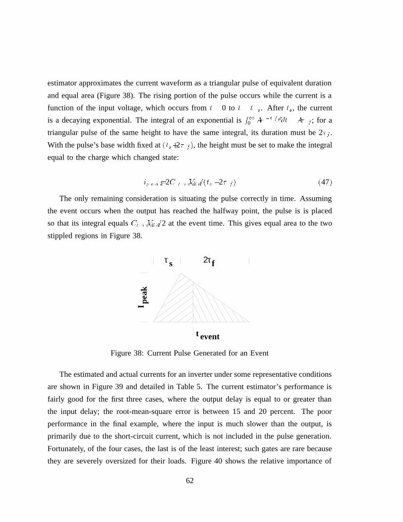
estimator approximates the current waveform as a triangular pulse of equivalent duration
and equal area (Figure 38). The rising portion of the pulse occurs while the current is a
function of the input voltage, which occurs fromt =0 to t =t s. After ts, the current
is a decaying exponential. The integral of an exponential isR1
0 Ae t = fdt =A f ; for a
triangular pulse of the same height to have the same integral, its duration must be 2f .
With the pulse’s base width fixed at(ts+2 f), the height must be set to make the integral
equal to the charge which changed state:
ip e a k=2C l o a dVd d=(ts +2 f) (47)
The only remaining consideration is situating the pulse correctly in time. Assuming
the event occurs when the output has reached the halfway point, the pulse is is placed
so that its integral equalsCl o a dVd d=2 at the event time. This gives equal area to the two
stippled regions in Figure 38.
t event
2τfτ s
I pea
k
Figure 38: Current Pulse Generated for an Event
The estimated and actual currents for an inverter under some representative conditions
are shown in Figure 39 and detailed in Table 5. The current estimator’s performance is
fairly good for the first three cases, where the output delay is equal to or greater than
the input delay; the root-mean-square error is between 15 and 20 percent. The poor
performance in the final example, where the input is much slower than the output, is
primarily due to the short-circuit current, which is not included in the pulse generation.
Fortunately, of the four cases, the last is of the least interest; such gates are rare because
they are severely oversized for their loads. Figure 40 shows the relative importance of
62

various input/output slope pairs for a typical MIPS-X simulation run. The graph on the
left shows the number of events occuring for each slope ratio; the graph on the right
weights these events by the capacitance of the node changing state. Unsurprisingly, the
most common occurance is for the input and output slopes to be approximately equal.
These events, along with the transitions of large, heavily-loaded drivers which appear in
the rightmost column, dominate the power dissipation.
tin > tout
tin = tout
tin < tout
tin = 0
0 1 2 3 4 5 6 7 8time (ns)
0
0.5
1.0
1.5
curr
ent (
mA
)
0
0.5
1.0
1.5
curr
ent (
mA
)
0
0.5
1.0
1.5
curr
ent (
mA
)
0
0.5
1.0
1.5
curr
ent (
mA
)
0
0.5
1.0
1.5
curr
ent (
mA
)
0
0.5
1.0
1.5
curr
ent (
mA
)
0
0.5
1.0
1.5
curr
ent (
mA
)
0
0.5
1.0
1.5
curr
ent (
mA
)
Figure 39: Pulses for Various Input and Output Slopes
63

Spice RsimInput Output Peak Time of Peak Time of rms
Waveform Risetime Delay Current Peak Current Peak errorA (ti n=0) 0 2.3ns 1.2mA 0ns 1.5mA 0 0.16mA
B (ti n to u t) 0.4ns 1.5ns 1.1mA 1.6ns 1.3mA 0.8ns 0.18mAC (ti n to u t) 1.0ns 1.0ns 0.9mA 2.2ns 1.0mA 1.8ns 0.15mAD (ti n to u t) 2.0ns 0.5ns 0.5mA 2.6ns 0.5mA 2.7ns 0.11mA
Table 5: Comparison of Current Pulses for Various Input and Output Slopes
Tin/Tout
≥10/19/18/17/16/15/14/13/12/11/11/21/31/41/51/61/71/81/9≤1/10
Cha
rge
Del
iver
ed
Tin/Tout
≥10/19/18/17/16/15/14/13/12/11/11/21/31/41/51/61/71/81/9≤1/10
Num
ber
of E
vent
s
Figure 40: Typical Input/Output Slope Distribution
64
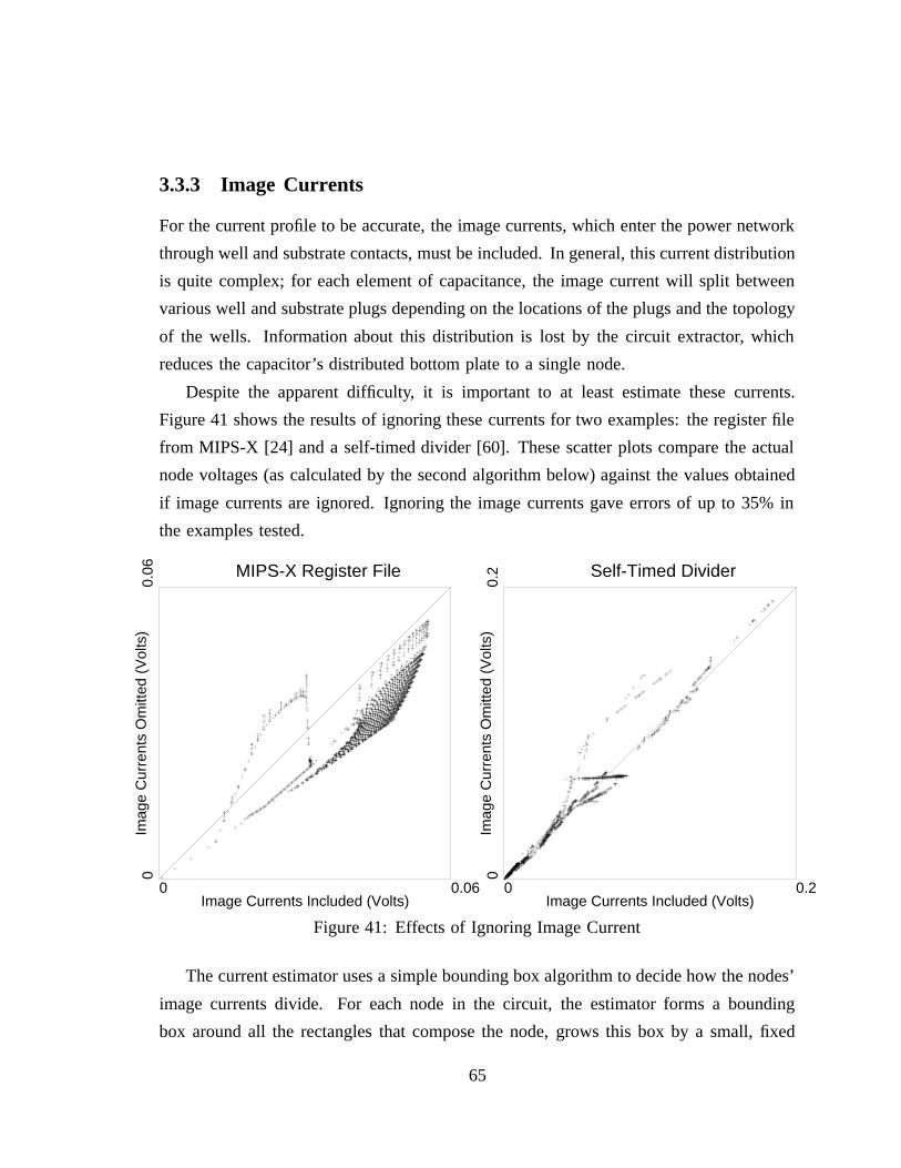
3.3.3 Image Currents
For the current profile to be accurate, the image currents, which enter the power network
through well and substrate contacts, must be included. In general, this current distribution
is quite complex; for each element of capacitance, the image current will split between
various well and substrate plugs depending on the locations of the plugs and the topology
of the wells. Information about this distribution is lost by the circuit extractor, which
reduces the capacitor’s distributed bottom plate to a single node.
Despite the apparent difficulty, it is important to at least estimate these currents.
Figure 41 shows the results of ignoring these currents for two examples: the register file
from MIPS-X [24] and a self-timed divider [60]. These scatter plots compare the actual
node voltages (as calculated by the second algorithm below) against the values obtained
if image currents are ignored. Ignoring the image currents gave errors of up to 35% in
the examples tested.
Self-Timed Divider
0 0.2Image Currents Included (Volts)
00.
2Im
age
Cur
rent
s O
mitt
ed (
Vol
ts)
MIPS-X Register File
0 0.06Image Currents Included (Volts)
00.
06Im
age
Cur
rent
s O
mitt
ed (
Vol
ts)
Figure 41: Effects of Ignoring Image Current
The current estimator uses a simple bounding box algorithm to decide how the nodes’
image currents divide. For each node in the circuit, the estimator forms a bounding
box around all the rectangles that compose the node, grows this box by a small, fixed
65

distance, and searches this area for substrate contacts of the correct type. Whenever the
node changes value, the estimator evenly divides the substrate current between all the
plugs in the box. If no plugs are found initially, the estimator doubles the box size and
repeats the search.
Node_B
Node_AN1
N3
P3 P4
P2
P1 N2
N4
P5
Figure 42: Bounding Box Current Estimation
This algorithm is easy to implement in Magic’s hierarchical, corner-stitched database.
The current estimator creates a special plane, into which it copies all the plugs encountered
during resistance extraction. When the regular extractor, which hierarchically calculates
connectivity and capacitance, processes a cell, it forms a bounding box for each node.
During the conversion of this hierarchical extracted description into a flat netlist suitable
for simulation, the bounding boxes are also combined to form a single box for each node.
Using Magic’s standard area searching routines, the estimator can find each node’s plugs
by searching the plug plane using this box.2
2This special plane is actually redundant; the temporary cell created to hold the flattened bus alreadyhas copies of all the plugs. However, the time to search a given area in a corner-stitched database isbasically proportional to the numbers of items that it contains; this regular plane that contains plugs alsocontains transistors, polysilicon, and diffusion. Using a separate plane speeds up searching by drasticallyreducing the number of tiles that the current estimator has to traverse.
66

For some nodes, like NodeA in Figure 42, this approximation is a fairly reasonable
one. The estimator spreads the current between plugs near the node, in this caseN1-N4
andP1-P2, which mimics what actually happens. The approximation is less accurate for
nodes containing ‘doglegs’, such as nodeB. Although the bounding box encloses node
N4, no current fromB will enter the bus there because the node does not extend over
N4’s well.
To test the validity of the bounding box algorithm, a more accurate estimate of
the image currents is needed. One method would be to calculate for each point in the
substrate how current injected there would divide between the various plugs. The fraction
of a node’s current that will flow to a given plug could then be set by integrating the
capacitance of each element of the node times the fraction that flows to the plug from
the points under that element. By repeating this for all plugs and all nodes in the circuit,
the estimator can get an accurate value for the entire current.
Calculating how an injected current would split from each point in the substrate could
be done using finite element techniques, but this would be extremely slow and memory-
intensive, and would preclude comparison on any but the simplest of examples. Instead,
the extractor assigns each point in a nwell or pwell region to the plug nearest it, as shown
in Figure 43. The estimator then re-extracts each node in the circuit and subdivides the
image current based on the capacitance to each plug’s subregion.
Even with the simplification on substrate subdivision, this method is still too memory-
intensive to run on an entire design. Instead, I ran it on some smaller circuits: MIPS-
X’s register file (10159 transistors), and the self-timed divider (5777 transistors). A
comparison of the bounding box and re-extraction algorithms is shown in Figure 44. In
both cases, the agreement between the two methods is quite good; it is better in the
register file because it contains fewer ‘dogleg’ wires.
3.3.4 Coupling Capacitance
Coupling capacitance is tricky to handle correctly because it is difficult to keep track of
where the capacitor’s bottom plate is connected. In Figure 45, a falling transition on
Nodeout1 will give two different current distributions depending on the value of Node
67
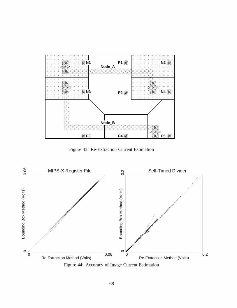
Node_B
Node_AN1
N3
P3 P4
P2
P1 N2
N4
P5
Figure 43: Re-Extraction Current Estimation
Self-Timed Divider
0 0.2Re-Extraction Method (Volts)
00.
2B
ound
ing
Box
Met
hod
(Vol
ts)
MIPS-X Register File
0 0.06Re-Extraction Method (Volts)
00.
06B
ound
ing
Box
Met
hod
(Vol
ts)
Figure 44: Accuracy of Image Current Estimation
68

out2. If out2 is low, then the capacitor is discharged in a local loop; ifout2 is high,
then the capacitor is charged through the power supply.
B
A
C
D
out1
out2
C1 C1
CAout2=0
C1
A
D
+-
out2=1
Figure 45: Effects of Coupling Capacitance
The relative importance of coupling capacitance varies with the design being analyzed.
For the three test designs, Figure 46 shows the division of the bottom plate capacitance
for all the chip’s signal capacitance.CGND andCV d dare the portions of the capacitance
whose bottom plate is connected to one of the power supplies,Cp a dis the (estimated)
off-chip capacitance that the chip outputs must drive,Cc o u p l eis the coupling capacitance
between on-chip signals, andCg a t eis the gate to channel capacitance.
I have listedCg a t eseparately because its behavior is fairly complex. It is a substrate
capacitance when the device is off, a coupling capacitance to the source terminal when
the device is saturated, and a coupling capacitance to both the source and drain when
the transistor is in the linear region. The channel capacitance only couples the gate to a
diffusion terminal when the gate-source or gate-drain voltage is greater than the threshhold
voltage, which generally occurs when the source is being pulled low. This requirement
virtually eliminates the Miller effect; the majority of the capacitance is to the transistor
source, which is not changing value. Since the channel capacitance is generally either
to a signal line that is being pulled to a supply voltage or to the substrate, the system
treats it as ground capacitance for n-channel devices and Vdd capacitance for p-channel
69
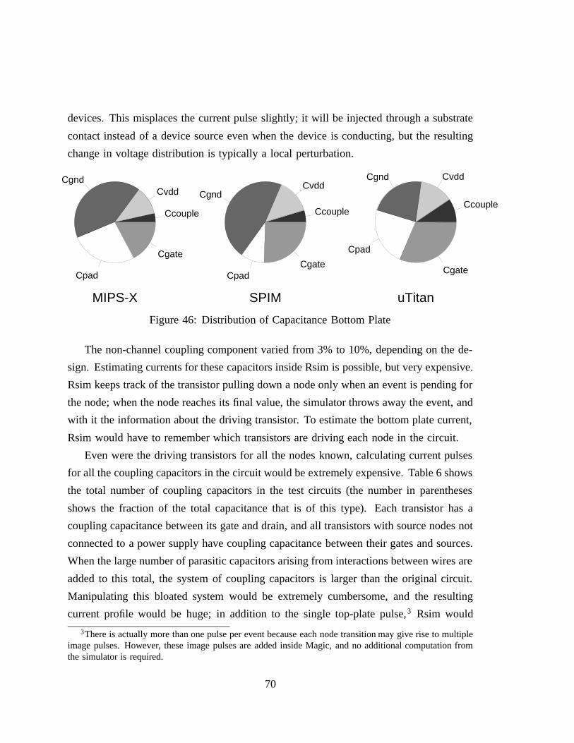
devices. This misplaces the current pulse slightly; it will be injected through a substrate
contact instead of a device source even when the device is conducting, but the resulting
change in voltage distribution is typically a local perturbation.
MIPS-X
Ccouple
CvddCgnd
Cpad
Cgate
SPIM
Ccouple
CvddCgnd
CpadCgate
uTitan
Ccouple
CvddCgnd
Cpad
Cgate
Figure 46: Distribution of Capacitance Bottom Plate
The non-channel coupling component varied from 3% to 10%, depending on the de-
sign. Estimating currents for these capacitors inside Rsim is possible, but very expensive.
Rsim keeps track of the transistor pulling down a node only when an event is pending for
the node; when the node reaches its final value, the simulator throws away the event, and
with it the information about the driving transistor. To estimate the bottom plate current,
Rsim would have to remember which transistors are driving each node in the circuit.
Even were the driving transistors for all the nodes known, calculating current pulses
for all the coupling capacitors in the circuit would be extremely expensive. Table 6 shows
the total number of coupling capacitors in the test circuits (the number in parentheses
shows the fraction of the total capacitance that is of this type). Each transistor has a
coupling capacitance between its gate and drain, and all transistors with source nodes not
connected to a power supply have coupling capacitance between their gates and sources.
When the large number of parasitic capacitors arising from interactions between wires are
added to this total, the system of coupling capacitors is larger than the original circuit.
Manipulating this bloated system would be extremely cumbersome, and the resulting
current profile would be huge; in addition to the single top-plate pulse,3 Rsim would
3There is actually more than one pulse per event because each node transition may give rise to multipleimage pulses. However, these image pulses are added inside Magic, and no additional computation fromthe simulator is required.
70

have to add an additional pulse for each coupling capacitor. Since the total coupling
capacitance is not that large, the estimator instead makes two simple approximations.
First, the gate-drain parastic capacitance is doubled to account for the Miller effect, as is
the gate-source capacitance for devices not collected to a supply. Coupling capacitances
for the wire parasitics are not doubled because transitions for their two terminals are much
less likely to be correlated. Second, the estimator assumes that the capacitor bottom
terminal is always at the opposite potential from the top terminal, so that a charging
current is generated. This produces larger voltage drops than would a discharging current
because charging currents go through the power supply.
CapacitorOrigin MIPS-X SPIM uTitanTransistor 47136 (1%) 41804 (1.5%) 179390 (4%)Gate-DrainTransistor 15333 (0.3%) 10364 (0.3%) 62433 (1%)Gate-SourceWire 76538 (2%) 72585 (3%) 260311 (4.5%)Parasitics
Total 139007 124753 502134
Nodes 17430 16614 61468
Table 6: Comparison of Nodes and Coupling Capacitors in Test Circuits
3.3.5 Charge Sharing
In a CMOS circuit, not all node transitions are caused by the connection of nodes to the
power supplies; sometimes the charge necessary to change a node’s value comes from
another node, as shown in Figure 47. Although the top plate current comes from another
node, the substrate current still comes though the supply network. Thesecharge sharing
events present different problems for the current estimator than do regular driven events.
To estimate how important estimating charge sharing currents is to power estimation,
I modified Rsim to record the type of each event when it is scheduled. In Chu’s modified
version of Rsim[12], there are three types of events: normal driven events, pure charge
71
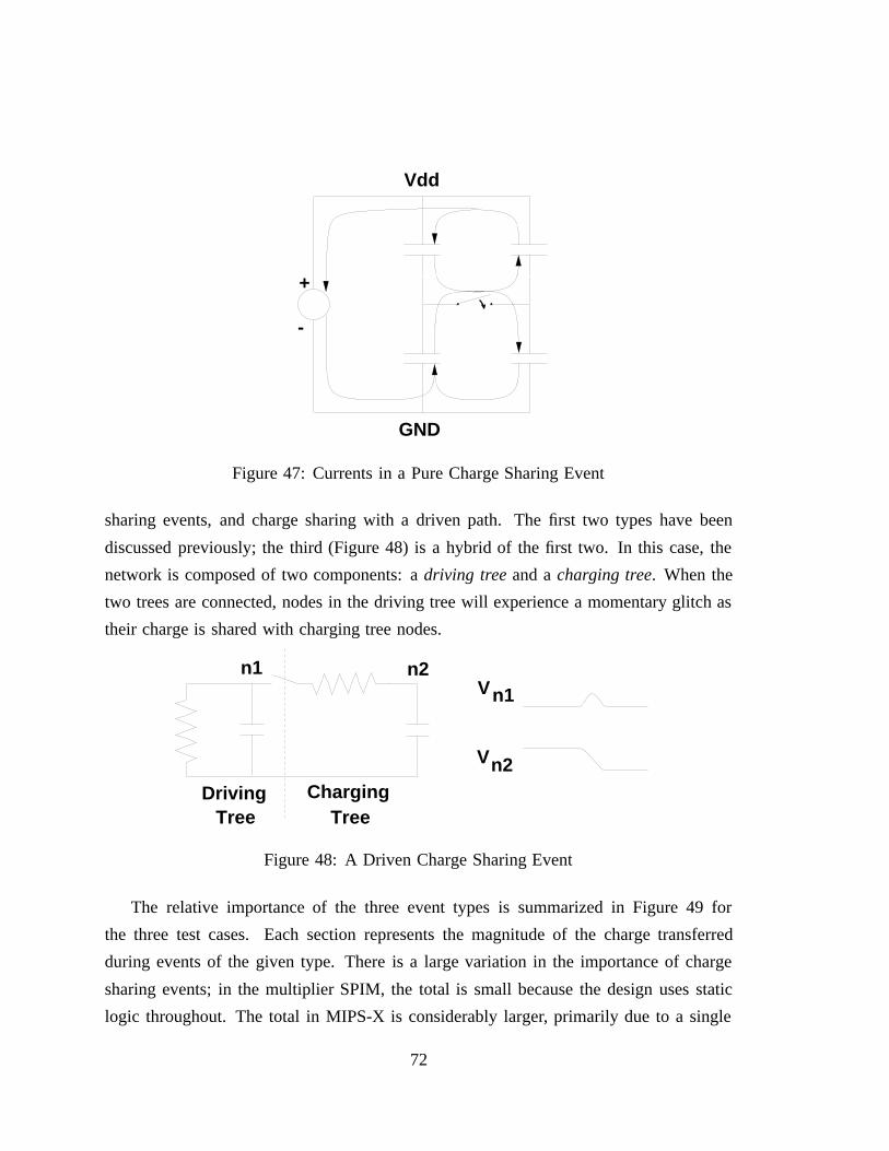
+
-
Vdd
GND
Figure 47: Currents in a Pure Charge Sharing Event
sharing events, and charge sharing with a driven path. The first two types have been
discussed previously; the third (Figure 48) is a hybrid of the first two. In this case, the
network is composed of two components: adriving treeand acharging tree. When the
two trees are connected, nodes in the driving tree will experience a momentary glitch as
their charge is shared with charging tree nodes.
n1 n2
DrivingTree
ChargingTree
Vn1
Vn2
Figure 48: A Driven Charge Sharing Event
The relative importance of the three event types is summarized in Figure 49 for
the three test cases. Each section represents the magnitude of the charge transferred
during events of the given type. There is a large variation in the importance of charge
sharing events; in the multiplier SPIM, the total is small because the design uses static
logic throughout. The total in MIPS-X is considerably larger, primarily due to a single
72
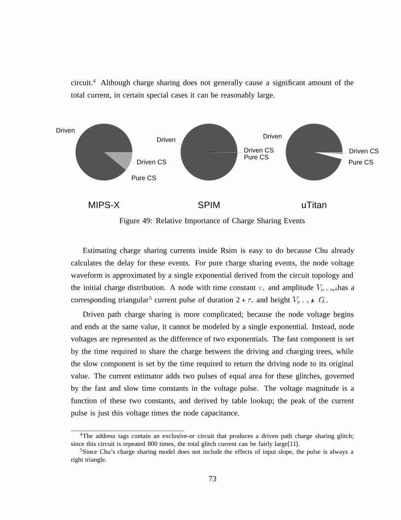
circuit.4 Although charge sharing does not generally cause a significant amount of the
total current, in certain special cases it can be reasonably large.
MIPS-X
Driven
Pure CS
Driven CS
SPIM
Driven
Pure CSDriven CS
uTitan
Driven
Pure CS
Driven CS
Figure 49: Relative Importance of Charge Sharing Events
Estimating charge sharing currents inside Rsim is easy to do because Chu already
calculates the delay for these events. For pure charge sharing events, the node voltage
waveform is approximated by a single exponential derived from the circuit topology and
the initial charge distribution. A node with time constante and amplitudeVp e a k, has a
corresponding triangular5 current pulse of duration 2 e and heightVp e a k CL.
Driven path charge sharing is more complicated; because the node voltage begins
and ends at the same value, it cannot be modeled by a single exponential. Instead, node
voltages are represented as the difference of two exponentials. The fast component is set
by the time required to share the charge between the driving and charging trees, while
the slow component is set by the time required to return the driving node to its original
value. The current estimator adds two pulses of equal area for these glitches, governed
by the fast and slow time constants in the voltage pulse. The voltage magnitude is a
function of these two constants, and derived by table lookup; the peak of the current
pulse is just this voltage times the node capacitance.
4The address tags contain an exclusive-or circuit that produces a driven path charge sharing glitch;since this circuit is repeated 800 times, the total glitch current can be fairly large[11].
5Since Chu’s charge sharing model does not include the effects of input slope, the pulse is always aright triangle.
73

3.3.6 Glitches
Glitches, changes in a signal that do not extend from one supply to the other, are difficult
to estimate in a Boolean timing simulator. The nor gate of Figure 50 shows one such
example. When InputA falls, Nodeout begins to rise. Before it reaches its final value,
however, InputB rises, causingout to fall again. Inside Rsim, an event is scheduled for
out afterA falls; before the event time reaches the simulation time,B rises and the event
is deleted from the queue. The simulated waveform for nodeout never changes value,
and no current pulse is generated for the event.
A
B
Out actualsimulated
A
B
A B
Out
Figure 50: Effects of a Node Glitch
To estimate the importance of this effect, I modified Rsim to keep track of the number
of events deleted from the queue and to estimate the amount of charge that these deleted
events contain. The charge estimate was produced by integrating each current waveform
from its beginning up to the time that the event was deleted. The results are shown
in Table 7. Although the number of events deleted can be fairly high, the amount of
current that they represent is quite small, indicating that most are removed soon after
scheduling. Since they represent such a small fraction of the total current, the system
can safely ignore them.
74

Percentage of Percentage ofDesign Events Deleted Charge Deleted
MIPS-X 14% 1.2%SPIM 7.6% 1.1%uTitan 7.0% 0.25%
Table 7: Importance of Glitch Currents
3.4 Performance
Current profiles for the three examples were obtained by applying test scripts supplied
by the designers to the circuits. Each script initialized a circuit’s state, enabled current
profiling, then exercised the design using some representative patterns. Table 8 compares
the elapsed time in seconds for these runs with those of an Rsim binary that does not
contain logging.6 The degree to which logging slowed down execution varied consider-
ably with the test patterns. The most elaborate script, used on the uTitan design, spent a
much larger fraction of its time setting up the state of the machine prior to logging than
did the other two. Since the logging module adds little overhead when it is not enabled,
the relative cost of logging is lower.
Circuit MIPS-X uTitan SPIM
Without Logging 198s 841s 71sWith Logging 287s 899s 100sLogging Cost 45% 6.9% 41%
Table 8: Rsim Running Times for Test Circuits
Table 9 shows where Rsim spends the extra running time of logging. For all three
designs, the extra time is dominated by simply writing the current profile to disk. The
row marked “Other” represents degradation in performance due to memory effects; the
logging version of Rsim has a larger working set.
6The tests were run on a Decstation 5000/200, which contains a 25Mhz R3000 CPU, 64Kb instructionand data caches, and 128Mb of memory. Both binaries were compiled with optimization level “-O4”.
75

Circuit MIPS-X uTitan SPIM
Tracing of Currents 4.5% 2.0% 3.0%Pulse Shape Calculation 13.5% 10% 16.5%Writing Log File 71.5% 57% 51.0%Other 10.5% 31% 29.5%
Table 9: Time Spent in Various Operations During Logging
Although logging slows down Rsim markedly, the degradation should not preclude
producing a current profile for any circuit which Rsim can handle. Since the standard
methodology is to run Rsim without logging until the circuit is functionally correct, then
to rerun the same script with logging enabled, adding current estimation does not lengthen
the crucial modify-simulate-debug cycle.7
The raw events produced by Rsim need considerable massaging before they are fed
to the linear solver. This is done inside Magic during resistance extraction. Each current
pulse is matched up with the correct transistor and plug nodes in the resistor network
and scaled by the fraction of capacitance to each supply. Once the pulses are matched up
and subdivided, their current is summed for all the transistors and plugs, and written to a
file for each user-specified time interval. The fraction of time required to perform these
operations is shown in Table 10. The variation in time between designs is dominated
primarily by the length of the pulse log. The one exception is the ground bus forTitan;
since the design does not have front side substrate contacts, the system does not have to
create separate image pulses for each event.
Despite the complications presented by pattern dependence and image currents, a
switch-level based estimator does a reasonable job producing current profiles for the
system. Rsim is not unacceptably slower during current logging, and the log produced
can be converted into a profile which correctly matches the resistance network in a modest
amount of processing time.
7This is not quite true because an Rsim binary containing logging runs about 5% slower even withlogging disabled due to slightly larger data structures. If this 5% is important, however, two binaries canbe used, one with the logging module and one without it.
76
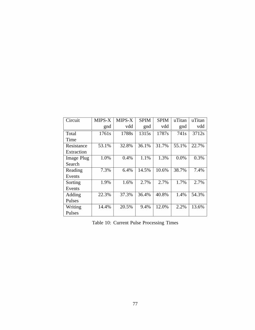
Circuit MIPS-X MIPS-X SPIM SPIM uTitan uTitangnd vdd gnd vdd gnd vdd
Total 1761s 1788s 1315s 1787s 741s 3712sTimeResistance 53.1% 32.8% 36.1% 31.7% 55.1% 22.7%ExtractionImage Plug 1.0% 0.4% 1.1% 1.3% 0.0% 0.3%SearchReading 7.3% 6.4% 14.5% 10.6% 38.7% 7.4%EventsSorting 1.9% 1.6% 2.7% 2.7% 1.7% 2.7%EventsAdding 22.3% 37.3% 36.4% 40.8% 1.4% 54.3%PulsesWriting 14.4% 20.5% 9.4% 12.0% 2.2% 13.6%Pulses
Table 10: Current Pulse Processing Times
77

Chapter 4
Current Estimation for ECL
All streams run to the sea,
but the sea is not full;
to the place where the streams flow,
there they flow again.
Ecclesiastes 1:7
In the estimation of current for CMOS circuits described in the last chapter, the
current distribution’s time dependency was of paramount importance. Information about
state changes in the circuit, distribution of nodal capacitance, and substrate topology had
to be considered to produce a reasonable current pattern. Fortunately, the process is
considerably less convoluted for ECL designs. In ECL, the magnitude of the current is
relatively fixed; all the logic does is steer current through different branches of the circuit.
As will be seen, this mode of operation simplifies current estimation considerably.
This chapter is divided into five sections. The first discusses the effects of supply
noise on ECL circuits and contrasts them to the corresponding effects for CMOS. Next
is a description of a simple current tracing algorithm suitable for estimating currents in
most gates, followed by extensions necessary to handle more specialized configurations.
Following this is a section describing techniques for handling the pattern dependence
of ECL circuits, and a discussion of the current estimator’s performance on some large
designs.
78

4.1 Introduction
Noise affects ECL circuits differently than it does MOS designs. Figure 51 shows the
effects of voltage drops along both supplies. Drops along the top rail,Vcc, shift a gate’s
transfer curve down, thereby reducing the circuit’s high noise margin. Drops along the
bottom rail,Vee, between a bias generator a current source reduce the gate’s signal swing,
reducing the gate’s low noise margin. The signal swing in ECL gates is set just large
enough to accommodate these and other sources of noise; the designer would like to
insure that the actual noise present is less that the margin allotted.
R Vee
R Vcc
Out
In Vbb
IL
R VeeIL
R VccILV in
Vo
ut
Bias
Figure 51: Effects of Noise on ECL Circuits
Figure 52 shows the current for a single gate. There are two components: the tail
currentIs t a t i cand the capacitive currentId y n. In contrast to CMOS circuits, the capacitive
component does not dominate in ECL designs. Equations 48 and 49 give the relation
between the static and dynamic currents for an emitter follower during transitions. The
static current controls the follower’s fall time, while the dynamic current controls the rise
time. In general, the designer will want the rise and fall times for the gate to be more or
less equal, so the peak magnitude of the dynamic current will be roughly equal to that of
79

the static current. The follower output is not always changing state, however. Equation
50. gives the total dynamic output current. The first term in the equation describes the
magnitude of the current when the output rises1, while the second two terms give the
number of transitions that actually occur.
Is t a t i c=CLVs wi n gtf a l l
(48)
Id y n=CLVs wi n g
tr i s e=tf a l l
tr i s eIs t a t i c (49)
Id y n=(tf a l l
tr i s eIs t a t i c)(
Cycles changing stateTotal cycles
)(tr i s e
tc y c l e) (50)
Although the second term in Equation 50, which is data dependent, may be unity for
some perverse selection of inputs, the final term will be considerably less than one; an
individual gate delay is substantially less than the cycle time of the system. This final
term, combined with the fact that the dynamic and static currents from a gate changing
state are roughly equal, explains why the dynamic current is less important than the static
current for the system as a whole.
Although the magnitude of the current is relatively fixed, the current pattern for each
gate still varies. In Figure 53, the current will enter theVcc bus at either point P1 or
P2, depending on the voltage at nodeIn . In the example, these points are not very far
apart, but in some circuits, such as a wired-or configuration or a decoder with shared
current line outputs, they may be. For ECL circuits, producing a current pattern includes
several tasks: calculating of the magnitude of the current, tracing the possible locations
in the circuit where the current may enter the power network, and choosing between
these locations.
4.2 Basic Current Tracing
The estimator’s first tasks are finding all the current sources in the design, marking the
locations where each current source connects toVee, then tracing up through the network1The formulation for a falling transition is similar, except that the total current through Vcc is reduced
by the dynamic current, and its magnitude is always equal or less than the static current.
80

Istatic
Idyn
Istatic
Figure 52: Currents for an ECL Gate
to find where these currents may enterVcc. This section describes the basic current
tracing algorithm; the next extends it to handle more complicated structures.
For simplicity, the current estimator makes two assumptions: it assumes that the diode
drop VBE is fixed for all transistors, and that the base current each transistor draws is zero.
Since designers typically run all transistors at near the same current density to preserve
the circuit’s noise margins, and the base current for unsaturated transistors is a small
fraction of the total, these approximations should not appreciably affect the estimator’s
accuracy.
Prior to tracing the currents, the estimator makes an initial pass over the network
to assign the direction of current flow for resistors. The tracing algorithm assumes that
current always flows through resistors in the same direction; from terminal 0 to terminal
1 in Figure 54. The estimator assigns a direction for each resistor using a set of rules
similar to those Jouppi uses to assign signal flow direction in MOS circuits[26]:
1. The high voltage supplyVcc is always terminal 0.
2. The low voltage supplyVee is always terminal 1.
3. For all the resistors not connected to a supply, the estimator checks the other devices
connected to each of the resistor’s nodes. If one end has only emitter connections
81

Out
In Vbb
Vee
P1 P2
P3
Vcs
Vcc
Vee
P3
P2
P1
Vcc
Figure 53: Locations of Currents for a Single Gate
and the other only collector connections, then the emitter end is terminal 0 and the
collector terminal 1.
n0
n1
Vcc
Vee
Figure 54: Direction of Current Flow in Resistors
Not all devices can be assigned a direction with these simple rules. An example of this
is the temperature compensation circuit shown in Figure 55. The current estimator cannot
assign a direction to resistor R2 because both its terminals are connected to transistor
emitters. When a resistor cannot be assigned current flow direction, the estimator removes
it from the circuit and optionally issues a warning to the designer.
82

Vcc
R0 R1
R2
Figure 55: Temperature Compensation Circuit
Once all resistors have been assigned a direction, the estimator calculates the voltage
and current ranges that each node and element can assume. Starting at the design’s
reference voltages, the estimator uses four basic rules:
1. Propagate voltages from base to emitter of a transistor and from terminal 0 to
terminal 1 of a resistor. The estimator sets the voltage at a node to the maximum
of the voltages at each base node minus a diode drop and the voltages at the top
nodes of each resistor minus the resistor voltage drop.
2. Propagate currents from emitter to collector of a transistor and from terminal 1 to
terminal 0 of a resistor. For each device, keep track of whether the current flowing
though it isnonswitchedor switched; a nonswitched current always flows though
the device, while a switched current may flow through the device depending on
the state of the circuit.
3. Resistors connected toVee form current sources. When the voltage at terminal 0
is set, calculate the current in the resistor and propagate it up the tree.
4. Resistors connected toVcc form loads. When the current in the resistor is known,
set the voltage at terminal 1 and propagate it to all connected bases.
83

800Ω
800Ω
P1 P2
1mA
1mA
1mA
1mA
1mA
Vcs=-3.6
e1=-4.4v
P1 P2
Vin=-0.8v, -1.6v
Vbb=-1.2v
e0=-1.6v,-2.0v
c0=0v, -0.8v
-5.2v
R1
Q1 Q2
Q3
R2
Figure 56: Tracing of Currents
Example 56 shows these rules in operation. Initially, the voltages ranges are known
for nodesVcs, Vin , andVbb. Starting at these nodes, the estimator sets the voltages at
the emitters of transistors Q1, Q2, and Q3. For nodee0, the maximum voltage is set one
diode drop below the maximum voltage atVin , and the minimum voltage is set one diode
drop below the voltage atVbb. For nodee1, the voltage is similarly fixed by nodeVcs.
Once the voltage ate1 is known, the estimator recognizes that R2 is a current source, and
sets its value to 1 mA. This current is then propagated up the tree, to transistors Q1, Q2,
and Q3, and resistor R1. Once the current in R1 is set, the estimator recognizes that it is
a load, and sets the voltage range atc0. Since the current through R1 is switched, the
voltage atc0 is set toVcc,Vcc+I1R1. With this gate finished, the estimator can continue
the process for other gates with inputs connected to nodec0.
In the example, the estimator does not really need to calculate the voltages at any
node excepte1 in order to trace the currents properly; setting voltage ranges for the rest
of the circuit seems extraneous. A simpler scheme might be to identify one signal as the
84

current source reference and assume that all transistors with bases connecting to it form
current sources. The current estimator uses the more general method for two reasons.
First, in some design methodologies, emitter followers have a resistor instead of a current
source connecting them toVee. Without knowing the voltage range at the base of the
emitter follower transistor, the current estimator cannot accurately calculate the emitter
follower current. Calculating voltage ranges for all the nodes in the system also allows
the current estimator to double as a ‘syntax’ checker for ECL circuits; it can identify
inputs connected at the wrong level, transistors pushed into saturation, and similar simple
errors, saving the designer time in debugging the circuit.
4.3 Advanced Structures
Unfortunately, not all circuits can be solved using the basic algorithm. The range of
circuits that designers use include some configurations more complicated than the basic
ECL current tree. These include resistors used to split currents, current trees that cannot
be correctly traced without some knowledge of the underlying logic, and diode structures.
This section describes extensions that allow analysis of these more complex circuits.
4.3.1 Switched and Split Currents
The algorithm description glossed over how the estimator determines whether a current
is switched or nonswitched. This is actually a fairly complicated problem; while being
steered through a gate, currents may split and reconverge in several places. One example
of this is shown in Figure 57. Current is switched between resistors R2 and R3 by the
differential pair of Q1 and Q2. The current reconverges at R1, however, regardless of the
circuit state. In order to correctly set the node voltages, the estimator has to determine
that the current from R4 is switched through R2 and R3 but not through R1.
This is done in two steps. The estimator first does a breadth first search of the circuit,
starting atVcc. Each device is assigned a number corresponding to the level at which
it was first encountered. In the example, R1 is a level 0 device, R2 and R3 are level 1
devices, Q1 and Q2 are level 2 devices, Q3 is a level 3 device and R4 is at level 4. Once
85

R1
R2 R3
Q1 Q2
Q3
R4
Switched
Unswitched
Figure 57: Switched and Unswitched Currents
each device has been assigned a level, the estimator traces out the currents as described
in the previous step. In tracing up the tree, the current is considered unswitched until
a differential pair is encountered. For the devices in the differential pair and above, the
current is labelled switched. Once all the currents have been traced through the tree, the
estimator counts the number of devices at level 0 through which each switched current
passes. If there is only one level 0 device, the current for this device is changed from
switched to unswitched, and any node voltages that are set by the element are updated.
This is repeated at each successive level until one is found where the current passes
through more than one device.
Implicit in the previous discussion of switched currents is the assumption that the
entire current is steered to one branch of the tree or the other; some configurations
violate this assumption. An example is shown in Figure 58. All the memory cells are
connected to a single current source, with the resistors at the bottoms of cells used to
subdivide the current between them.
86

Figure 58: Resistor Divided Currents
Calculating precisely how the currents split is difficult. Since each node is represented
by a voltage range rather than a single value, the diode-resistor current divider model
employed by Bisim[29] cannot be used. Instead, the estimator assumes that the current
divides evenly between all the resistors. When the current is propagated further up the
tree, it is tagged with the amount of current that is actually passing through the particular
branch. Thus, as the estimator traces each current up the tree, it attaches to each device
encountered a pointer to the resistor forming the current source, a flag describing whether
the current is switched or unswitched, and a label giving the fraction of the current that
passes through this branch of the tree.
4.3.2 Logic Dependent Circuits
Not all circuits can be correctly traced knowing only the voltage ranges at each node;
for some, the estimator must also understand properties of the underlying logic function.
The 4-bit barrel shifter of Figure 59 is one example. Although any of the four currents
IA-ID can be steered to any of the four loads, R1- R4, each load will receive at most one
current at any given time because only one of select linesS0-S3 will be active. If the
estimator does not understand this logic dependency, it will set the swings at the outputs
to four times their actual values.
87

S0
S1
S2
S3
S3 S2 S1R1
R2
R3
R4
IA IB I C ID
Vcc
Figure 59: Barrel Shifter
Another state dependent circuit is the current source shared between many decoder
outputs shown in Figure 60. Without knowing that only one of the decoder outputs will
be high, the estimator will divide the current evenly between all the resistors. Although
the voltage ranges for the outputs will be correct, the current will be smeared over all
the outputs; any voltage drop problems associated with the large peak currents will not
be caught.
In the general case, determining that a set of nodes have this mutual exclusivity
property, where only one is high at any given time, is too expensive to calculate. Instead,
the estimator provides two simpler mechanisms for incorporating logic dependencies.
It recognizes decoder circuits (described in the next section) and marks their outputs as
88
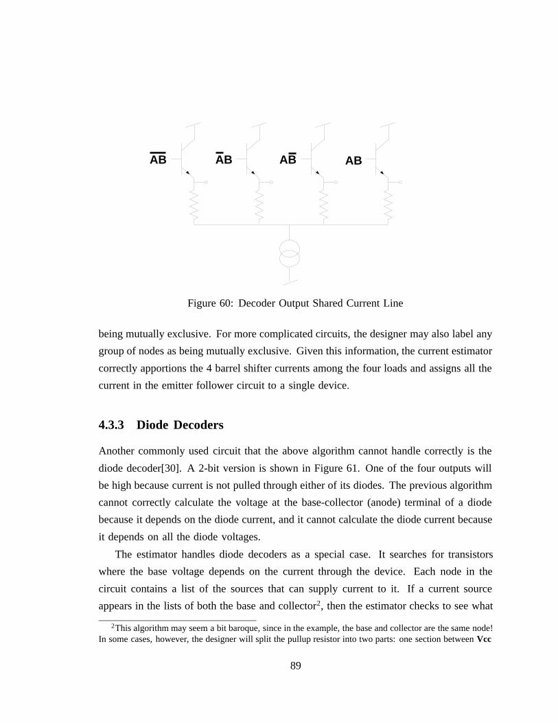
ABAB AB AB
Figure 60: Decoder Output Shared Current Line
being mutually exclusive. For more complicated circuits, the designer may also label any
group of nodes as being mutually exclusive. Given this information, the current estimator
correctly apportions the 4 barrel shifter currents among the four loads and assigns all the
current in the emitter follower circuit to a single device.
4.3.3 Diode Decoders
Another commonly used circuit that the above algorithm cannot handle correctly is the
diode decoder[30]. A 2-bit version is shown in Figure 61. One of the four outputs will
be high because current is not pulled through either of its diodes. The previous algorithm
cannot correctly calculate the voltage at the base-collector (anode) terminal of a diode
because it depends on the diode current, and it cannot calculate the diode current because
it depends on all the diode voltages.
The estimator handles diode decoders as a special case. It searches for transistors
where the base voltage depends on the current through the device. Each node in the
circuit contains a list of the sources that can supply current to it. If a current source
appears in the lists of both the base and collector2, then the estimator checks to see what
2This algorithm may seem a bit baroque, since in the example, the base and collector are the same node!In some cases, however, the designer will split the pullup resistor into two parts: one section betweenVcc
89
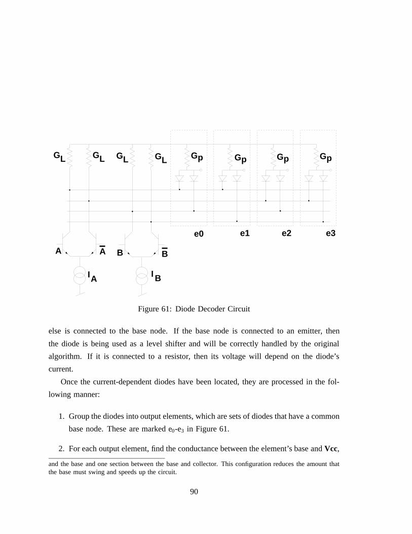
e0 e1 e2 e3
Gp Gp Gp Gp
IA I B
A B BA
GL GL GLGL
Figure 61: Diode Decoder Circuit
else is connected to the base node. If the base node is connected to an emitter, then
the diode is being used as a level shifter and will be correctly handled by the original
algorithm. If it is connected to a resistor, then its voltage will depend on the diode’s
current.
Once the current-dependent diodes have been located, they are processed in the fol-
lowing manner:
1. Group the diodes into output elements, which are sets of diodes that have a common
base node. These are marked e0-e3 in Figure 61.
2. For each output element, find the conductance between the element’s base andVcc,
and the base and one section between the base and collector. This configuration reduces the amount thatthe base must swing and speeds up the circuit.
90
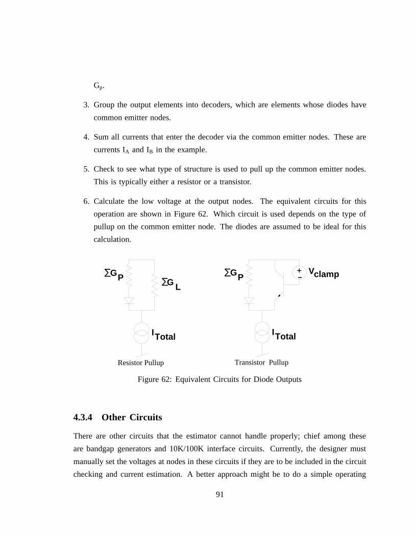
Gp.
3. Group the output elements into decoders, which are elements whose diodes have
common emitter nodes.
4. Sum all currents that enter the decoder via the common emitter nodes. These are
currents IA and IB in the example.
5. Check to see what type of structure is used to pull up the common emitter nodes.
This is typically either a resistor or a transistor.
6. Calculate the low voltage at the output nodes. The equivalent circuits for this
operation are shown in Figure 62. Which circuit is used depends on the type of
pullup on the common emitter node. The diodes are assumed to be ideal for this
calculation.
ITotal
Resistor Pullup
ITotal
Transistor Pullup
+-
VclampGPΣLGΣ
GPΣ
Figure 62: Equivalent Circuits for Diode Outputs
4.3.4 Other Circuits
There are other circuits that the estimator cannot handle properly; chief among these
are bandgap generators and 10K/100K interface circuits. Currently, the designer must
manually set the voltages at nodes in these circuits if they are to be included in the circuit
checking and current estimation. A better approach might be to do a simple operating
91
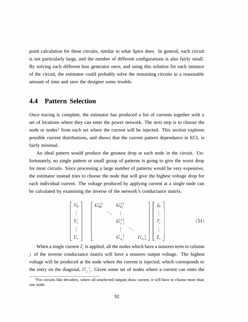
point calculation for these circuits, similar to what Spice does. In general, each circuit
is not particularly large, and the number of different configurations is also fairly small.
By solving each different bias generator once, and using this solution for each instance
of the circuit, the estimator could probably solve the remaining circuits in a reasonable
amount of time and save the designer some trouble.
4.4 Pattern Selection
Once tracing is complete, the estimator has produced a list of currents together with a
set of locations where they can enter the power network. The next step is to choose the
node or nodes3 from each set where the current will be injected. This section explores
possible current distributions, and shows that the current pattern dependance in ECL is
fairly minimal.
An ideal pattern would produce the greatest drop at each node in the circuit. Un-
fortunately, no single pattern or small group of patterns is going to give the worst drop
for most circuits. Since processing a large number of patterns would be very expensive,
the estimator instead tries to choose the node that will give the highest voltage drop for
each individual current. The voltage produced by applying current at a single node can
be calculated by examining the inverse of the network’s conductance matrix.
266666666664
V0...
Vj...
Vn
377777777775=
266666666664
G100 G1
0j. . .
...
G1j j
.... . .
G1n j G1
n n
377777777775
266666666664
I0...
Ij...
In
377777777775
(51)
When a single currentIj is applied, all the nodes which have a nonzero term in column
j of the inverse conductance matrix will have a nonzero output voltage. The highest
voltage will be produced at the node where the current is injected, which corresponds to
the entry on the diagonal,G1j j. Given some set of nodes where a current can enter the
3For circuits like decoders, where all unselected outputs draw current, it will have to choose more thanone node.
92
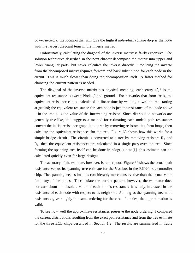
power network, the location that will give the highest individual voltage drop is the node
with the largest diagonal term in the inverse matrix.
Unfortunately, calculating the diagonal of the inverse matrix is fairly expensive. The
solution techniques described in the next chapter decompose the matrix into upper and
lower triangular parts, but never calculate the inverse directly. Producing the inverse
from the decomposed matrix requires forward and back substitution for each node in the
circuit. This is much slower than doing the decomposition itself. A faster method for
choosing the current pattern is needed.
The diagonal of the inverse matrix has physical meaning; each entryG1j j is the
equivalent resistance between Nodej and ground. For networks that form trees, the
equivalent resistance can be calculated in linear time by walking down the tree starting
at ground; the equivalent resistance for each node is just the resistance of the node above
it in the tree plus the value of the intervening resistor. Since distribution networks are
generally tree-like, this suggests a method for estimating each node’s path resistance:
convert the initial resistance graph into a tree by removing resistors that form loops, then
calculate the equivalent resistances for the tree. Figure 63 shows how this works for a
simple bridge circuit. The circuit is converted to a tree by removing resistors R4 and
R6, then the equivalent resistances are calculated in a single pass over the tree. Since
forming the spanning tree itself can be done innlog(n) time[1], this estimate can be
calculated quickly even for large designs.
The accuracy of the estimate, however, is rather poor. Figure 64 shows the actual path
resistance versus its spanning tree estimate for theVcc bus in the R6020 bus controller
chip. The spanning tree estimate is considerably more conservative than the actual value
for many of the nodes. To calculate the current pattern, however, the estimator does
not care about the absolute value of each node’s resistance; it is only interested in the
resistance of each node with respect to its neighbors. As long as the spanning tree node
resistances give roughly the same ordering for the circuit’s nodes, the approximation is
valid.
To see how well the approximate resistances preserve the node ordering, I compared
the current distributions resulting from the exact path resistance and from the tree estimate
for the three ECL chips described in Section 1.2. The results are summarized in Table
93
1Ω
1.625 Ω
4Ω
Original Network Actual Path Resistances Tree Path Resistances
1Ω
1Ω
1Ω
1Ω1Ω
1Ω
1Ω1Ω
1.625 Ω
3Ω
2Ω 3Ω
2Ω2Ω
Figure 63: Tree Path Resistance Example
114. The two current distributions are nearly identical; in the worst of the circuits, less
than 3% of the current pattern changed.
Figure 65 shows the effect of the current pattern change for the R6020. Using the path
resistance approximation made essentially no difference in the final voltage distribution
in any of the chips tested. Since the calculation of tree path resistances is two orders of
magnitude faster, the pattern selector uses it to assign current locations.
4.5 Performance
Current profiles for the three designs were obtained by running the ECL current estimator
on netlists extracted from the chip layouts. The results are summarized in Table 12.
Analysis of fairly reasonably sized designs is thus possible in a modest amount of time.
Given that the current estimator can produce patterns for fairly large designs, the other
4The tests were run on a MipsCo RC3260, which contains a 25Mhz R3000 CPU, 64Kb instruction anddata caches, and 128Mb of memory. The program was compiled with optimization level “-O4” and rununder RISC/os 4.50.
94

R6020 MMU
0 7Exact Path Resistance (ohms)
07
Tre
e P
ath
Res
ista
nce
(ohm
s)
Figure 64: Spanning Tree Estimate of Path Resistance
consideration is the quality of the highest marginal cost current pattern. Underlying this
question is a more fundamental one: how much effect does the state of the circuit really
have on the current pattern? In most ECL gates, the location where current enters the
power bus will not vary greatly; like the example in Figure 53, the variousVcc connec-
tions are close together. Only in a few classes of circuits, such as wired-or configurations
and decoders with a shared current output, are the points likely to be very far apart. To
test how much variation there is in the voltage distribution, I applied two different current
distributions to each circuit in the R6000 chipset. The first distribution was calculated
using the highest marginal cost criterion described in this section. The second was pro-
duced by using alowest marginal cost function, which produces the smallest possible
drop for each individual current. Figure 66 contains scatter plots comparing the two. In
general, the correlation is fairly good, indicating that the design is not particularly pattern
dependent. Variations from perfect correlation seem to fall into two categories: nodes
either form a line that diverges upward from perfect correlation (as seen in the center
of the R6000 plot) or they come in pairs, one above and one below the center diagonal.
95

R6000 R6010 R6020Chip CPU FPC SBC
Total nodes 71947 72052 59495in Vcc busNodes with 16610 15992 16075current appliedNodes where 3 19 477pattern variedExact method 6.1 hours 5.8 hours 6.1 hoursRunning timeTree method 1.8 minutes 1.8 minutes 1.5 minutesRunning time
Table 11: Comparison of Current Pattern Selection Methods
Circuit R6000 R6010 R6020
Running Time 552s 354s 803sMemory Usage 15.5Mb 19.9Mb 17.2Mb
Table 12: Running Times for ECL Current Estimation
The first pattern corresponds to a circuit where all the possible locations for a current
fall in the same branch of the network; by choosing the node farthest from the pad,
the highest marginal cost algorithm shifts up the voltage for all the intervening points
in the branch. The second pattern occurs when the current’s locations fall in different
branches of the network; switching between locations causes one branch’s node voltages
to increase while those of the other branch decrease.
The highest marginal cost function seems to be modestly better than just picking
current locations at random, but not spectacularly so. In the three examples, 65% of
the nodes had equal or higher voltages for the highest marginal cost pattern than for the
lowest marginal cost. Despite the relative insensitivity of ECL current patterns to the
state of the circuit, I decided to continue using the highest marginal cost current pattern.
Since the network solution techniques described in the next chapter require formation of
96

R6020 MMU
0 50Exact Pattern (mV)
050
Tre
e P
atte
rn (
mV
)
Figure 65: Effects of Path Resistance Estimate on Voltages
a spanning tree for the network anyway, the overhead involved in implementing the cost
function is minimal. Further, more specialized circuits that make greater use of wired-or
circuits, such as Ling Adders[33], may have a greater pattern dependence than do the
R60X0 chips, which are composed primarily of ordinary gates.
Given the relative insensitivity of the ECL current distribution to the circuit state, and
the ease with which a single, static current pattern can be calculated, the static current
estimation algorithm described in this chapter is sufficient for current estimation in ECL
designs.
97

R6000 CPU
0 80Lowest Marginal Cost (mV)
080
Hig
hest
Mar
gina
l Cos
t (m
V)
R6010 FPC
0 110Lowest Marginal Cost (mV)
011
0H
ighe
st M
argi
nal C
ost (
mV
)
R6020 SBC
0 50Lowest Marginal Cost (mV)
050
Hig
hest
Mar
gina
l Cos
t (m
V)
Figure 66: Current Pattern Dependence of ECL circuits
98

Chapter 5
Network Solution
Our life is frittered away by detail. An honest man has hardly need to count
more than his ten fingers, or in extreme cases he may add his ten toes, and
lump the rest. Simplicity, simplicity, simplicity!
Henry David Thoreau
Walden (1854)
The last three chapters described how to derive a resistance network from the design’s
layout and a current profile from its circuit; the remaining step is solving for the network’s
node voltages and branch currents. When run on an entire design, the number of node
equations can be fairly large; networks of order 20,000 are not uncommon[54]. Since
the current distribution can vary with time, these systems may have to be solved more
than once. Fortunately, power supply networks have some special properties that allow
for faster calculation of voltages.
The first section of this chapter outlines previous approaches that have been taken to
solve these networks. Following this is an examination of some of the special properties
of resistor networks and how they can be exploited, an outline of applicable sparse matrix
techniques, and a discussion of the system’s performance on the test designs.
99

5.1 Previous Work
Branin[4] solves power supply networks using tree-link analysis. He envisions power
supply networks as being basically trees, with an occasional loop created when the de-
signer adds cross links. Figure 67 shows what happens when a single link resistorRl i n k
is added to a tree, forming a loop. The link resistor takes some amount of current from
one branch of the tree and redistributes it to the other. Current is only affected in the
loop formed by the link and the two sides of the tree connecting to it; the currents above
the top nodeN0, where the two branches merge, is unchanged.
R0
R1R2
R3
R4 R5Rlink
N0
N2
N1
N4
N3
N5
A
1kΩ
1kΩ1kΩ
1kΩ
1kΩ 1kΩ
4V
6V
5V 5V
7V 7V
1mA 1mA
1mA 1mAB
1kΩ
1kΩ1kΩ
1kΩ
1kΩ 1kΩ
4V
5.5V
5.5V
6V
5V
6.5V
-.5mA
C
Figure 67: A Single Link Resistor in a Tree
Isolated link resistors in a tree-like structure thus add local perturbations to the un-
derlying tree voltage-current distribution. This suggests a method for solving this class
of network:
1. Form a spanning tree for the network.
2. Solve the tree network, ignoring all non-tree resistors.
3. Calculate the perturbations in the current distribution caused by the link (non-tree)
resistors.
100

4. Solve the network again using the revised current distribution.
Branin’s algorithm is efficient for systems where the number of loops is quite small.
The most expensive step in the algorithm is usually calculating the loop currents. As the
number of loops go up, the complexity of the system of loop equations also goes up.
While it is reasonable to assume that the number of loops is small in circuits fabricated
with a single layer of metal, it is not true for newer devices that have meshes embedded in
their power distribution networks. However, this algorithm can still be used to advantage
in some limited cases, as discussed in Section 5.3.
Tyagi[58] uses a method similar to Branin’s, except that the range of topologies that
it can handle is more limited. He also assumes that the network is basically a tree, except
for some comb sections at the tree’s leaves. Combs are sections of power bus that have
parallel wires tied together at both ends. Each comb section is treated as a supernode; all
the current that enters the network through the comb section is injected at node where the
comb is attached to the tree. The tree and comb are then solved separately; the tree using
the linear two-pass algorithm discussed in the next section and the comb by solving the
node-current equations. For a comb, Tyagi shows that the node equations can be solved
in linear time.
Partitioned NetworkOriginal Network
Tree Section Comb Section
Figure 68: Tyagi’s Algorithm for Treelike Systems
Most of the power networks in custom designs could not be solved using this algorithm
because they do not have a tree-comb topology. Even if more general networks than
101

combs are allowed for the non-tree sections, Tyagi’s approach will be fairly slow; a
single loop near the root of a power bus will cause nearly all of the bus to be put in a
single supernode. Solution time for this supernode will be essentially the same as the
time required for directly solving the original network. Since any distribution topology
that has more than one pad connection will haveall nodes (including the root node)
as part of a loop, Tyagi’s method is not particularly useful for contemporary multilayer
power networks.
Chowdhury[10] takes a different approach to analyzing the system. Rather than
calculating the actual node voltages and branch currents, he instead calculates an upper
bound on the current that can flow through each branch assuming that some subset of
the network branches fail via electromigration. Figure 69 shows an example of how his
algorithm works. For each node, the estimator enumerates all possible paths to ground.
Picking such a path divides the nodes in the design into two classes: those whose current
may flow to the node and through the path to ground, and those whose current will not.
In the example, starting at noden2 and using the pathe1 e0, current from nodesn1,
n2, andn3 fall into the first class and nodesn0 andn4 fall into the second one. Once
the nodes have been classified, the maximum current for the first element in the path
can be determined; it is the sum of the currents from all the nodes in the first set. In
the example, the maximum current in elemente1 for the given starting node and path is
In 1+I n 2+I n 3. By repeating this operation for all nodes and paths in the system, the
maximum current in each branch can be calculated.1
Unfortunately, the upper bound that this algorithm gives for each element is much too
conservative to be useful. Figure 70 represents the power distribution for the datapath
section of the design. There is one horizontal power line for each bit in the datapath,
with vertical connections to pads at either end. Using Chowdhury’s algorithm, the upper
bound on the current in each element of each row is very nearly the entire current for
the datapath. The solid line represents one node-path pair; current may flow from nearly
all the nodes in the circuit to the node-path pair via the dotted lines. Each bit’s power
connection would have to be wide enough to support the current for all the bits. No
1Chowdhury does not actually evaluate every path; by using branch and bound techniques, he can showthat some paths will not give a larger current for the element than a path already enumerated, and cantherefore be ignored.
102

n0
n1
n2 n3
n4
e0e1
e2
e3
e4
e5
Figure 69: Chowdhury’s Max Current Estimation Algorithm
aggressive design can afford to be this conservative.
n
Figure 70: Overestimation in Chowdhury’s Algorithm
Since none of these algorithms were entirely satisfactory, I decided to take a closer
look at the designs to see what special properties they exhibited and how these properties
might be exploited. The techniques that the analyzer currently uses take some of the
more useful components of Branin’s algorithm for trees and simple links, and combine
them with a new algorithm for handling sections of resistors in series with interspersed
current sources.
103

5.2 Trees of Resistors
A typical power supply network in a VLSI design (Figure 71) consists of two sections:
a “backbone” that provides global distribution of power from the pads to the various
modules on chip, and a “feeder” network that connects individual cells and transistors
to the backbone. The most common style for these feeder networks is a tree, with the
root being the connection to the backbone and the leaves being each transistor connected
to the supply. Solving these tree networks is simple: starting at the leaves (Figure 72),
currents are summed up toward the root. Once the current is known in each branch, the
node voltages can be found by back-substitution; each node’s voltage is that of its parent
node plus the voltage drop across the connecting resistor.
PadPad
= Transistor
Figure 71: A Typical Power Network
In the linear solver, these trees are replaced on the network backbone by a current
source representing all the current injected into the tree. After the backbone network is
solved and the voltage at the root node of each tree is known, the leaf voltages can be
found by the method described above.
5.3 Simple Loops and Kirchoff’s Voltage Law
This section explores Branin’s algorithm in more depth. The key to his method is quickly
calculating the current disturbance caused by the link resistors. This adjustment can be
104
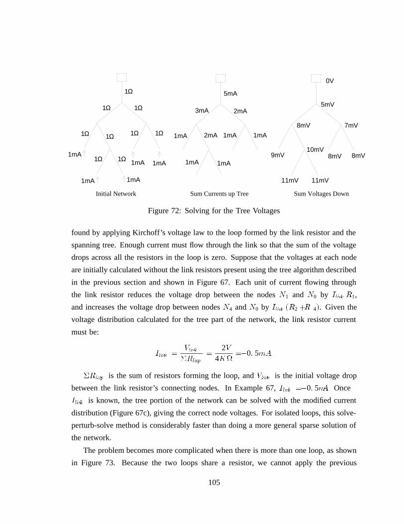
5mA
3mA 2mA
2mA1mA
1mA 1mA
1mA 1mA
0V
5mV
8mV 7mV
9mV10mV
11mV 11mV
8mV 8mV
Initial Network Sum Currents up Tree Sum Voltages Down
1mA
1mA
1mA
1mA1mA
1Ω
1Ω1Ω
1Ω
1Ω 1Ω
1Ω 1Ω
1Ω
Figure 72: Solving for the Tree Voltages
found by applying Kirchoff’s voltage law to the loop formed by the link resistor and the
spanning tree. Enough current must flow through the link so that the sum of the voltage
drops across all the resistors in the loop is zero. Suppose that the voltages at each node
are initially calculated without the link resistors present using the tree algorithm described
in the previous section and shown in Figure 67. Each unit of current flowing through
the link resistor reduces the voltage drop between the nodesN1 and N0 by Ilink R1,
and increases the voltage drop between nodesN4 andN0 by Ilink (R2 +R 4). Given the
voltage distribution calculated for the tree part of the network, the link resistor current
must be:
Ilink =VlinkRloop
=2V4K
=0: 5mA
Rloop is the sum of resistors forming the loop, andVlink is the initial voltage drop
between the link resistor’s connecting nodes. In Example 67,Ilink =0: 5mA. Once
Ilink is known, the tree portion of the network can be solved with the modified current
distribution (Figure 67c), giving the correct node voltages. For isolated loops, this solve-
perturb-solve method is considerably faster than doing a more general sparse solution of
the network.
The problem becomes more complicated when there is more than one loop, as shown
in Figure 73. Because the two loops share a resistor, we cannot apply the previous
105
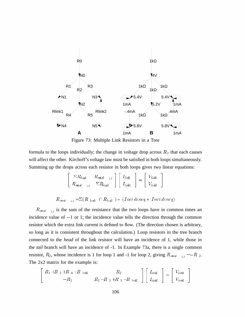
R0
R1R2
R3
R4 R5Rlink1 Rlink2
N0
N2
N1
N4
N3
N5
A
1kΩ
1kΩ1kΩ
1kΩ
1kΩ 1kΩ
4V
5.2V
5.4V 5.4V
5.8V 5.8V
-.4mA .4mA
1mA
1mA 1mA
1mA
B
Figure 73: Multiple Link Resistors in a Tree
formula to the loops individually; the change in voltage drop acrossR2 that each causes
will affect the other. Kirchoff’s voltage law must be satisfied in both loops simultaneously.
Summing up the drops across each resistor in both loops gives two linear equations:24 Rloop1 Rmutual 1;2
Rmutual 1;2 Rloop2
3524 Ilink1
Ilink2
35 =
24 Vlink1
Vlink2
35
Rmutual 1;2 =(R loop1 \Rloop2 ) (Inci dence1 Inci dence2)
Rmutual 1;2 is the sum of the resistance that the two loops have in common times an
incidencevalue of1 or 1; the incidence value tells the direction through the common
resistor which the extra link current is defined to flow. (The direction chosen is arbitrary,
so long as it is consistent throughout the calculation.) Loop resistors in the tree branch
connected to theheadof the link resistor will have an incidence of 1, while those in
the tail branch will have an incidence of -1. In Example 73a, there is a single common
resistor,R2, whose incidence is 1 for loop 1 and -1 for loop 2, givingRmutual 1;2 =R 2.
The 2x2 matrix for the example is:24 R1 +R 2 +R 4 +R link1 R2
R2 R2 +R 3 +R 5 +R link2
3524 Ilink1
Ilink2
35 =
24 Vlink1
Vlink2
35
106

This 2x2 system is trivially invertible, givingIlink2 =I link1 =0: 4mA. With the
link currents known, the tree can be solved again, giving the voltage distribution shown
in Figure 73b.
This method can be extended for an arbitrary number of link resistors. The resulting
system will have one equation per link resistor:
NXj=1
Rmutual i;j Ilink j
=V link i
Once this system is solved, currents in the tree portion of the network can be modified
and the corresponding node voltages calculated.
Unfortunately, this algorithm does not work well for most power networks. A net-
work’s backbone section generally contains many link resistors, each of which share part
of their loop with another link. This gives a large number of nonzeroRmutual terms,
making the resulting system, while lower order, considerably less sparse than the original.
Table 13 shows the sizes and number of nonzero terms for the power networks of the
three CMOS designs described in Section 1.2. The first two columns show the order
and sparsity for the conductance matrix after the simplification techniques have been
performed, while the latter two show the corresponding values for the mutual resistance
matrix. Using the sparse techniques discussed in Section 5.5, the higher order, sparser
systems can be solved more quickly than the more dense, lower order ones.
Unlike the original matrices, however, the mutual resistance matrix is usually dis-
connected. Each subgraph of the matrix corresponds to a set of link resistors with a
nonzero mutual resistance to at least one other member of the set, but no nonzero mutual
resistance values to anything else. The order of a subgraph is equal to the number of link
resistors it contains. Figures 67 and 73 show subgraphs of order 1 and 2, respectively.
Table 14 shows the distribution of subgraph orders for the designs mentioned above. All
the networks contain a random scattering of low order subgraphs and one or two high
order ones that contain the network “backbone”.
Several of the networks have a large number of subgraphs containing one or two
members. These sections usually arise from strapping a region with high sheet resistance,
such as diffusion, with a much less resistive one, such as metal. They are often part of a
107

Simplified Original Mutual ResistanceMatrix Matrix
Power Matrix Nonzero Matrix NonzeroNetwork Order Terms Order TermsMIPS-X gnd 4095 18019 2893 129401MIPS-X vdd 2881 11651 2469 35241SPIM gnd 2139 8737 1165 31085SPIM vdd 601 2443 324 26616Titan gnd 3066 12366 1669 13021Titan vdd 2123 3244 1157 32925
Table 13: Original and Mutual Resistance Matrices
Power Subgraph OrderNetwork 1 2 3-10 11-100 101-1000 1000MIPS-X gnd 15 3 5 4 0 1MIPS-X vdd 75 444 3 0 0 1SPIM gnd 0 0 1 3 0 1SPIM vdd 0 0 1 1 1 0Titan gnd 11 53 64 2 2 0Titan vdd 39 9 36 3 1 0
Table 14: Subgraph Sizes for Various Networks
feeder network that could have otherwise been removed by the tree algorithm described
above. Since these subgraphs are trivial to solve and removing them often allows an
entire subtree to be separated from the main graph, Ariel processes them specially. It
searches the resistor network for one and two element graphs that are part of trees which
can be removed from the network. When it finds one, Ariel replaces the subnetwork with
a current source as described in Section 5.2. Once the backbone network has been solved,
the voltages in the loop are determined by calculating the initial tree voltages, inverting
and solving the 1x1 or 2x2 loop-link matrices, and recalculating the tree voltages using
the modified current distribution.
Moderate sized subgraphs, containing less than 100 elements, can also be solved
108

relatively cheaply. Unfortunately, they are rarely parts of a feeder tree and therefore
cannot be separated from the main graph. Because of this, Ariel limits this type of
processing to 1 and 2 element subgraphs.
5.4 Series Connections of Resistors
Once the trees and simple loops are removed from a network, the remaining backbone
consists primarily of long strings of resistors, one per bit pitch, with occasional cross links,
as shown in Figure 74. These long sections of series resistors, with a current source at
each intervening node, can be replaced by a single resistor with a current source at each
end. An intuitive derivation of the equivalent circuit is given in the following section.
For the skeptical, a more formal derivation is given in Section 5.4.2.
PadPad
Figure 74: Power Network with Trees and Simple Loops Removed
5.4.1 Equivalent Circuit for Series Resistors
Consider the series chain in Figure 75a. There will be some voltage, VS, between the
two series ends, N1 and Nn. Conceptually, a voltage source with value VS can be added
between nodes N1 and Nn without disturbing the network. Superposition can be applied
to this network to produce the equivalent circuit shown in figure 75b. The equivalent
resistance RS is just the sum of all the resistors in series. Superposition can be used to
109

I1 I2 I3 In-1 In
R1 R2 Rn-1N1 N2 N3 Nn-1 Nn
+- Vs
A
Ie1 Ien
RSN1 Nn
B
Figure 75: Series Equivalent Circuit
determine how the current from each current source divides between the two ends. All
current sources except the one in question are replaced by open circuits, while the voltage
source between nodes N1 and Nn is replaced by a short circuit. The resulting system is a
simple current divider, and the additional current at N1 and Nn is just the sum of all the
divided currents:
RS =n1Xi=1
Ri (52)
Ie1 =nXi=1
Pn1j=i Rj
RS
Ii (53)
Ien =nXi=1
Pi1j=1 Rj
RSIi (54)
An arbitrarily long series of resistors can thus be replaced by a single resistor and
two current sources.
Once the network has been solved with the equivalent series circuit and the voltages
110
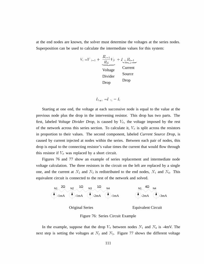
at the end nodes are known, the solver must determine the voltages at the series nodes.
Superposition can be used to calculate the intermediate values for this system:
Vi =V i1 +Ri1
RSVS| z
Voltage
Divider
Drop
+ I eiRi1| z Current
Source
Drop
Iei+1 =I ei Ii
Starting at one end, the voltage at each successive node is equal to the value at the
previous node plus the drop in the intervening resistor. This drop has two parts. The
first, labeledVoltage Divider Drop, is caused byVS, the voltage imposed by the rest
of the network across this series section. To calculate it,VS is split across the resistors
in proportion to their values. The second component, labeledCurrent Source Drop, is
caused by current injected at nodes within the series. Between each pair of nodes, this
drop is equal to the connecting resistor’s value times the current that would flow through
this resistor ifVS was replaced by a short circuit.
Figures 76 and 77 show an example of series replacement and intermediate node
voltage calculation. The three resistors in the circuit on the left are replaced by a single
one, and the current atN2 andN3 is redistributed to the end nodes,N1 andN4. This
equivalent circuit is connected to the rest of the network and solved.
-1mA -1mA -2mA -1mA
2Ω 1Ω 1ΩN1 N2 N3 N4
Original Series
-2mA -3mA
4ΩN1 N4
Equivalent Circuit
Figure 76: Series Circuit Example
In the example, suppose that the dropVS between nodesN1 andN4 is -4mV. The
next step is setting the voltages atN2 andN3. Figure 77 shows the different voltage
111

components for each node. The voltage divider drops are calculated by partitioningVS
between the three resistors. The current source drop is found by calculating the current
that would flow through each resistor withN1 andN4 grounded. Beginning at the left,
the current between nodesN1 andN2 is Ie2 =I e1 I1 =1mA. Similarly, the current
betweenN2 andN3 is Ie3 =I e2 I1 =0. The current source drop in each section is the
resistance times these currents. The total drop for each node is calculated by adding the
two components.
-5mV
0mV
-1mV
-2mV
-3mV
-4mV
Actual Voltage
0mV
-1mV
-2mVCurrent Source Drop
0mV
-1mV
-2mV
-3mV
-4mVVoltage Divider Drop
4V 2Ω4Ω
-1mA 2Ω 2mA 1Ω
0mA 1Ω
4V 1Ω4Ω
4V 1Ω4Ω
N1 N2 N3 N4
Figure 77: Voltages for Series Circuit Example
5.4.2 Norton Equivalent Circuits for the Series Systems
The previous derivation and example were intended to be intuitive; this section gives
a more formal derivation of the series equivalent circuit. Figure 78a shows a series
of n resistors interspersed with current sources. RL and IL form the Norton equivalent
circuit representing the rest of the network as seen from the left end of the series. Figure
78b shows the series equivalent circuit for this configuration, as derived in the previous
112
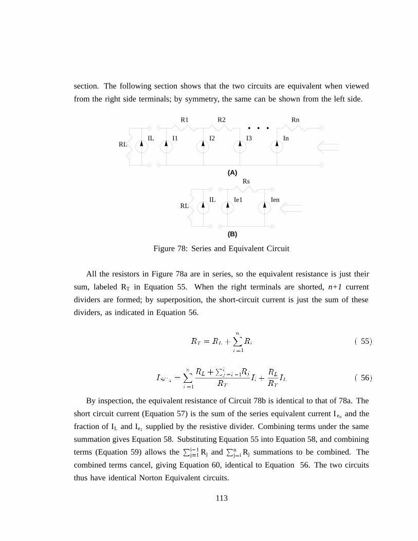
section. The following section shows that the two circuits are equivalent when viewed
from the right side terminals; by symmetry, the same can be shown from the left side.
IL I1 I2 I3 InRL
R1 R2 Rn
(A)
IL Ie1 IenRL
Rs
(B)
Figure 78: Series and Equivalent Circuit
All the resistors in Figure 78a are in series, so the equivalent resistance is just their
sum, labeled RT in Equation 55. When the right terminals are shorted,n+1 current
dividers are formed; by superposition, the short-circuit current is just the sum of these
dividers, as indicated in Equation 56.
RT = RL +nXi =1
Ri ( 55)
ISCA =nXi =1
RL +Pi
j =i 1Rj
RTIi +
RL
RTIL ( 56)
By inspection, the equivalent resistance of Circuit 78b is identical to that of 78a. The
short circuit current (Equation 57) is the sum of the series equivalent current Ien and the
fraction of IL and Ie1 supplied by the resistive divider. Combining terms under the same
summation gives Equation 58. Substituting Equation 55 into Equation 58, and combining
terms (Equation 59) allows thePi1
j=1 Rj andPn
j=i Rj summations to be combined. The
combined terms cancel, giving Equation 60, identical to Equation 56. The two circuits
thus have identical Norton Equivalent circuits.
113
ISCB =nXi =1
Pi 1j =1RjPnj =1Rj
Ii +RL
RT( IL +
nXi =1
Pnj =iRjPnj =1Rj
Ii) ( 57)
ISCB =nXi =1
RT (Pi 1
j =1Rj) +RL(Pn
j =iRj)
RT (Pn
j =1Rj)Ii +
RL
RTIL ( 58)
ISCB =nXi =1
(Pi 1
j =1Rj) (Pn
j =1Rj) +RL(Pi 1
j =1Rj +Pn
j =iRj)
RT (Pn
j =1Rj)Ii +
RL
RTIL ( 59)
ISCB =nXi =1
Pi 1j =1Rj +RL
RTIi +
RL
RTIL ( 60)
5.5 Network Solution Techniques
Once all the above simplifications have been performed on a network, the remainder
is basically a mesh representing the backbone of the power distribution system. The
voltage distribution of this network must be calculated. The following two sections
examine methods for solving this network.
5.5.1 Direct Methods
The power network can be be written as ann-1by n-1 system of equations Gv= i, where
G is the conductance matrix, v are the voltages at then-1 nodes (referenced to ground),
and i are the currents injected at these nodes. Since G is positive definite,2 there exists a
Cholesky decomposition G= LLt, where L is lower triangular. Once this decomposition
is known, the node voltages v can be calculated by forward solving the lower triangular
system Ly= i, then back substituting into Ltv = y to derive v.
The key to this algorithm is being able to calculate the LLt factorization quickly.
This is done using an envelope implementation of the bordering method as described by
2A positive definite matrix is one for which xtAx > 0 for all x with at least one nonzero element. Forthe conductance matrix G, the term vtGv has a physical interpretation; since Gv is the current injectedat each node, vtGv= vti. The inner product vti is the power dissipated by the network, which is alwaysgreater than zero for nonzero excitation. Conductance matrices are thus positive definite due to the law ofconservation of energy.
114

George[16]. The matrix G can be written as a matrix M of ordern-1, a column vectoru
representing thenth row, and a diagonal terms. Equation 63 gives the factorization of
G assuming that M’s factorization, LMLtM, is known.
G =
M u
ut s
( 61)
M = LMLtM ( 62)
G =
LM 0
wtps wtw
LtM w
0ps wtw
( 63)
w = L1M u ( 64)
The factorization can thus be computed starting at the upper left corner by setting
L0 =pg0; 0, then solving the lower triangular system L0w = u to calculate the second
row. Adding this row to L0 gives the decomposition L1Lt1 of the leading submatrix
M1. Each subsequent row can be solved in the same manner, using the factorization Li
calculated in the previous step.
The only remaining problem is deciding the node ordering for the matrix. Ariel uses
the Reverse Cuthill-McKee method[18]. Given a starting node, its neighboring nodes are
added to the matrix in increasing order of degree. Neighbors of the nodes just added are
in turn sorted and included; this process continues until all nodes have been processed.
This ordering is then reversed because the opposite ordering has been proven to always
have an equal or smaller envelope than the forward one.
In processing CMOS power supply networks, the system of equations is usually solved
more than once. Once the conductance matrix G is factored, the cost of calculating each
time step is relatively small; it is just the time required to solve the two triangular systems.
Direct techniques thus look attractive for technologies where the power supply current is
dynamic.
115

5.5.2 Iterative Methods
Of the iterative solution methods, Successive Overrelaxation (SOR) seems to have the
most promise. For resistor networks, SOR is simply successive application of Kirchoff’s
Current Law:
Vit = ( 1 !) Vit 1+ !Ii +
Pnk=1GkVkPn
k=1Gk
Each new guess at a node’s voltage is derived by looking at the voltages of the
neighboring nodes, then setting the value so that KCL is obeyed for this node. The
overrelaxation factor! is required for fast convergence; without it, voltages approach
their final values very slowly.
The main disadvantage to overrelaxation is its sensitivity to the “diameter” of the
network, i.e. the number of edges separating the two nodes which are furthest apart.
Since each node directly affects only the voltages of its immediate neighbors, the number
of iterations it takes for changes in one node to propagate throughout the network is pro-
portional to the diameter. Fortunately, the simplification techniques previously described
either remove many of the “tall”, stringy sections of the network or replace them with
a single resistor, so the simplified network’s height is considerably less than that of the
original system.
5.6 Results
The effectiveness of the above simplification procedures on several designs is shown
in Figure 79. The total reduction in network size varied strongly with the network’s
topology; it ranged from a factor of 5 for one of the microprocessors to a factor of 50 for
the multiplier. The tree and series simplifications were effective on all three designs, but
the success of removing simple loops from the network varied widely. The pad drivers
for MIPS-X have one configuration that yields many such loops; removing them reduced
the total network size by 19%. However, in the multiplier, no simple loops were found.
Whether this simplification is worth implementing is dependent on design style.
Solution times using direct factorization are shown in Table 15. The program was
run on a Titan, an ECL RISC machine developed at the Digital Equipment Corporation
116

0
10000
20000
30000
Nodes
MIP
S-X
GN
D
MIP
S-X
Vdd
uTitan G
ND
uTitan V
dd
SP
IM G
ND
SP
IM V
dd
Tree Nodes EliminatedLoop Nodes EliminatedSeries Nodes EliminatedRemaining Nodes
Figure 79: Results of Network Reduction
Western Research Laboratory that is about 15 times faster than a VAX-11/780. “Setup”
includes the time required to calculate the LLt factorization, and “Solve” is the time
required to solve the two triangular systems Ly= i and Ltx = y and to do the back
annotation for the trees and series. (For comparison, solving the first network, ‘MIPS-X
gnd’, using spice2g6[39] on the same machine took about 14 hours.) The speedups here
for the smaller networks are less impressive because the solution time for a single voltage
vector is dominated by simply reading in the network. However, the speedup for each
additional solution (the ratio of the ‘Solve’ columns) is considerably higher; it ranges
between 4.5 and 254. This lower marginal cost for each additional solution permits a
larger number of current distributions to be applied to the network.
Solution times for both the original and simplified networks using the iterative method
are shown in Table 16. In this case, “Read” is the time required to parse the input file,
“Setup” is the time to identify the tree, loop, and series configurations, and “Solve”
is the time required to solve the core network and back-annotate the tree and series
voltages. The speedup obtained is roughly proportional to the amount by which the
original network could be reduced. The unsimplified networks for the second two designs
require significantly longer to solve than the first because their network diameter is higher.
117

Time in SecondsPower Unsimplified SimplifiedNetwork Read Setup Solve Read Setup Solve SpeedupMIPS-X gnd 26.8 293.6 9.64 26.8 56.8 2.0 3.8MIPS-X vdd 34.4 949.5 381.6 34.5 30.2 1.5 20.6Titan gnd 28.4 130.1 5.2 27.7 8.7 1.0 4.4Titan vdd 29.4 126.5 5.375 29.8 6.3 1.1 4.3SPIM gnd 36.6 161.1 6.4 36.5 6.67 1.3 4.6SPIM vdd 37.4 93.7 5.0 37.3 3.9 1.1 3.2
Table 15: Direct Method Solution Times
Of the two methods, direct solution looks more useful. It was faster for all but one
of the test cases listed, and for cases where the network is to be solved more than once
using different current distributions, each additional solution is relatively cheap.
Time in SecondsPower Unsimplified SimplifiedNetwork Read Setup Solve Read Setup Solve SpeedupMIPS-X gnd 26.8 3.2 235.1 27.5 2.9 42.8 3.6MIPS-X vdd 34.4 4.6 399.0 36.5 19.7 28.8 5.2Titan gnd 27.7 3.7 1640.0 28.3 3.8 220.8 6.6Titan vdd 29.3 3.8 1097.4 29.3 2.7 60.7 12.2SPIM gnd 36.6 5.0 1044.0 38.4 3.8 22.5 16.8SPIM vdd 37.3 5.0 2281.4 38.0 3.6 6.3 48.5
Table 16: Iterative Method Solution Times
5.7 Conclusions
Three algorithms for efficient partitioning of resistor networks into small sections that
can be solved quickly have been presented. The first algorithm analyzes trees by noting
that current always flows toward the tree’s root, the second processes simple loops using
118

Kirchoff’s Voltage Law, and the third solves series configurations using superposition.
The system remaining after such partitioning was readily solved using standard sparse
positive definite matrix techniques. Two such techniques were explored: direct solution
using the bordering method and iterative solution using successive overrelaxation. Solv-
ing using the partitioning algorithms provided an overall speedup between 3 and 50 for
the designs tested.
119

Chapter 6
Results
Glendower: I can call spirits from the vasty deep.
Hotspur: Why, so can I, or so can any man,
But will they come for you when you call for them?
William Shakespeare
1 Henry IV
The previous four chapters described how the system produces resistance, current,
and voltage profiles for the network. Now that the system is assembled, the next step is
to see what it can discover about some real designs. This chapter contains plots showing
the voltages and currents calculated by the system for the designs tested, and discusses
some of their salient features.
The voltage distribution of the metal ground bus from the MIPS-X microprocessor
datapath is shown in Figure 80. The values shown are the maximum over ten clock
cycles. Dots that are completely black represent nodes where the voltage drop is half a
volt or more. The datapath is connected to the padframe at the upper left and lower right
corners. There are several notable features in this plot. The black column of nodes in
the left side are part of the register file. In the MIPS-X architecture, Register 0 always
returns a value of 0; half of each register file cell in this column is hardwired to ground.
This connection is made in a peculiar way; the source of the access transistor is grounded
via a polysilicon wire. Most of the drop seen in the drawing is due to the polysilicon,
but it appears in the plot because of the small strip of metal required to connect between
120
polysilicon and diffusion.
The dark section in the upper left corner of the design is the floating point coprocessor
interface. As evidenced by the sharp gradient, power for this interface is not connected to
the rest of the datapath; instead of connecting to the clean power below it, the designer
inexplicably extended down lines from the clock driver circuitry that sits just above1.
The coprocessor interface bounces with the large transient voltages that occur when the
clocks switch.
There is also a horizontal dark patch in the upper right corner. At the right of the
datapath are the match tags for the instruction cache; sitting at the top of these tags are
some fairly large buffers that drive the block select signals into the instruction cache,
which sits above the datapath. These buffers are all powered via a minimum width metal
line, which bounces substantially when they change state.
Despite these shortcomings, however, the power distribution for MIPS-X is roughly
consistent with the designer’s expectations. The designers were assuming a 0.5V drop
on the supply lines; aside from the dummy register file column where the drop is not a
problem, this estimate seems reasonable.
For Titan, however, the voltage distribution plot highlights a substantial flaw in the
power bus wiring. Figure 81 shows the ground voltage drops for the metal section of the
microprocessor. At the top of the plot is the datapath, with the instruction cache sitting
below it. The internal power wiring of the instruction cache was not modeled, so this
section of the plot is blank. To the right of the instruction cache are a set of large drivers
for the cache’s column select and sense amplifier circuitry. The power wiring for these
drivers is 66m wide in the driver cells themselves, but is connected to the main power
bus by a 4m wide, 4mm long wire. The drop calculated along this wire is nearly two
volts. Since the amount of current drawn by the drivers will be noticably reduced by the
large ground bounce, the actual drop is somewhat lower.
Root-mean-square current densities forTitan’s ground bus are shown in Figure 82.
Predictably, the same icache wire that gave high voltage drops also carries a large current
density. (The actual density calculated for the wire is over 5 mA= m2; the scale has been
compressed to show detail in some of the lower current density areas.) There are some
1Sadly, I designed this section of the chip.
121

other areas where the current density is rather high. In the datapath, ground is wired
horizontally, with each two bits sharing a power line. There are few vertical connections
between these horizontal buses, and they seem susceptible to electromigration. Depending
on the data, the current drawn by each bit in the path will be different, as will the current
that each horizontal power line must carry. This sometimes gives substantial voltage
gradients between adjacent lines. At the occasional connections between these buses,
large currents flow to try and equalize the potential.
Figure 83 shows the ground voltage drops for the SPIM multiplier. Here the scale
runs from 0 to 1 volts; since the design is fully static, it does not have any functionality
problems from the high drops, but it is losing some speed. Power runs horizontally in the
design, with no vertical cross links, and adjacent power lines often have quite different
drops. One possible solution would be to make the array a little wider and add vertical
cross ties to spread the current move evenly among all the buses.
Figure 84 shows the root-mean-square current densities for SPIM. This plot is basi-
cally an inverse of the last one, with low current density grey in the center of the array
and high density black at the edges. The scale here runs to 5 mA= m2, indicating a
fairly aggressive design. It is probably worth considering widening these lines or adding
vertical cross links.
Figure 85 shows the voltage distribution for the ground bus of the R6000 micro-
processor, including package and bond wire drops. The on-chip voltage drops range
from 20mV to 130mV. The design uses a standard-cell methodology, with power running
horizontally in rows. The highest drops occur in the center section of standard cells,
which are the farthest from the pads. The two open squares in the bottom left corner
contain the register file cells; “ground” for the cells is a special reference voltage several
hundred millivolts below real ground. This extra space is necessary to allow the file’s
sense amplifier to operate properly. Since this virtual ground is not part of the actual
ground network, the arrays appear blank.
Total solution times for the test circuits are given in Table 17. The CMOS designs
were run on a 22 MHz Titan, an ECL RISC machine, while the ECL designs were run
on a MipsCo RC3260, which runs at 25 Mhz.
122

Unsurprisingly, solution times for the CMOS designs are dominated by generating
current patterns and solving the system. The SPIM times are the shortest, primarily
because the SPIM simulation uses the smallest number of current patterns (about 200)
compared to over 800 for MIPS-X and 600 forTitan.2 The solution times for Vdd and
Ground are roughly consistent for each design exceptTitan. This primarily arises from
two factors: substrate contacts and icache power routing. Since this design contains no
frontside substrate contacts, the resistance network for Ground is simpler, and the current
profile contains no additional image current pulses. In the instruction cache, Vdd is
gridded and Ground is not, giving Vdd a more complex network. These factors lead to
the wide disparity in solution times.
For the ECL designs, the situation is reversed; resistance extraction dominates. Since
the technology for these chips includes three layers of metal and and some 45-degree
angles, there are substantially more rectangles to process. Producing currents and solving
the system is fast because only one current distribution is involved, and the chips’ power
buses do not contain many meshes.
Time (seconds)Resistance Current System
Circuit Extraction Estimation Solution Total
MIPS-X Ground 933 1113 4829 6875MIPS-X Vdd 586 1488 2996 5070SPIM Ground 431 940 650 2021SPIM Vdd 567 1320 833 2720Titan Ground 408 1232 2612 4252Titan Vdd 843 3768 22130 26741R6000 Vcc 9168 537 106 9811R6010 Vcc 9392 360 106 9858R6020 Vcc 3788 802 88 4679
Table 17: Total Analysis Times
2These solution times differ from those in the last chapter for two reasons. First, the networks usedhere are somewhat larger; the extractor was not allowed to merge diffusion and metal resistors, so thatmetal-only drops could be calculated. Second, extra consistency, voltage and current density checks wereperformed on the networks after each solution step.
123

MIPS-X Ground Bus Voltage Drops
0V10.00mV20.00mV30.00mV40.00mV50.00mV60.00mV70.00mV80.00mV90.00mV0.10V0.11V0.12V0.13V0.14V0.15V0.16V0.17V0.18V0.19V0.20V0.21V0.22V0.23V0.24V0.25V0.26V0.27V0.28V0.29V0.30V0.31V0.32V0.33V0.34V0.35V0.36V0.37V0.38V0.39V0.40V0.41V0.42V0.43V0.44V0.45V0.46V0.47V0.48V0.49V0.50V
Fig
ure
80:
MIP
S-X
Gro
und
Bus
Vol
tage
Plo
t
124

uTitan Ground Voltage Drops
0V40.00mV80.00mV0.12V0.16V0.20V0.24V0.28V0.32V0.36V0.40V0.44V0.48V0.52V0.56V0.60V0.64V0.68V0.72V0.76V0.80V0.84V0.88V0.92V0.96V1.00V1.04V1.08V1.12V1.16V1.20V1.24V1.28V1.32V1.36V1.40V1.44V1.48V1.52V1.56V1.60V1.64V1.68V1.72V1.76V1.80V1.84V1.88V1.92V1.96V2.00V
Fig
ure
81:
uTita
nG
roun
dB
usV
olta
geP
lot
125

uTitan Ground Current Density
0A/um^250.00uA/um^20.10mA/um^20.15mA/um^20.20mA/um^20.25mA/um^20.30mA/um^20.35mA/um^20.40mA/um^20.45mA/um^20.50mA/um^20.55mA/um^20.60mA/um^20.65mA/um^20.70mA/um^20.75mA/um^20.80mA/um^20.85mA/um^20.90mA/um^20.95mA/um^21.00mA/um^21.05mA/um^21.10mA/um^21.15mA/um^21.20mA/um^21.25mA/um^21.30mA/um^21.35mA/um^21.40mA/um^21.45mA/um^21.50mA/um^21.55mA/um^21.60mA/um^21.65mA/um^21.70mA/um^21.75mA/um^21.80mA/um^21.85mA/um^21.90mA/um^21.95mA/um^22.00mA/um^22.05mA/um^22.10mA/um^22.15mA/um^22.20mA/um^22.25mA/um^22.30mA/um^22.35mA/um^22.40mA/um^22.45mA/um^22.50mA/um^2
Fig
ure
82:
uTita
nC
urre
ntD
ensi
ties
(rm
s)
126

SPIM Ground Voltage Drops
0V20.00mV40.00mV60.00mV80.00mV0.10V0.12V0.14V0.16V0.18V0.20V0.22V0.24V0.26V0.28V0.30V0.32V0.34V0.36V0.38V0.40V0.42V0.44V0.46V0.48V0.50V0.52V0.54V0.56V0.58V0.60V0.62V0.64V0.66V0.68V0.70V0.72V0.74V0.76V0.78V0.80V0.82V0.84V0.86V0.88V0.90V0.92V0.94V0.96V0.98V1.00V
Fig
ure
83:
SP
IMG
roun
dB
usV
olta
geP
lot
127
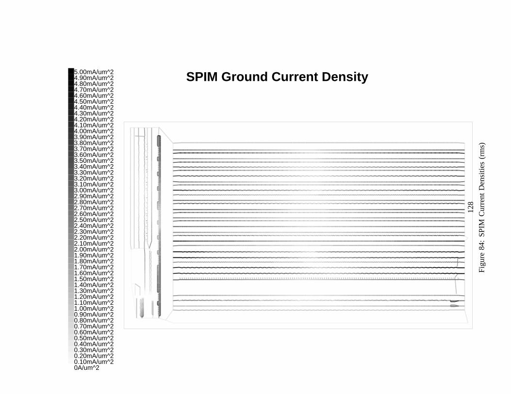
SPIM Ground Current Density
0A/um^20.10mA/um^20.20mA/um^20.30mA/um^20.40mA/um^20.50mA/um^20.60mA/um^20.70mA/um^20.80mA/um^20.90mA/um^21.00mA/um^21.10mA/um^21.20mA/um^21.30mA/um^21.40mA/um^21.50mA/um^21.60mA/um^21.70mA/um^21.80mA/um^21.90mA/um^22.00mA/um^22.10mA/um^22.20mA/um^22.30mA/um^22.40mA/um^22.50mA/um^22.60mA/um^22.70mA/um^22.80mA/um^22.90mA/um^23.00mA/um^23.10mA/um^23.20mA/um^23.30mA/um^23.40mA/um^23.50mA/um^23.60mA/um^23.70mA/um^23.80mA/um^23.90mA/um^24.00mA/um^24.10mA/um^24.20mA/um^24.30mA/um^24.40mA/um^24.50mA/um^24.60mA/um^24.70mA/um^24.80mA/um^24.90mA/um^25.00mA/um^2
Fig
ure
84:
SP
IMC
urre
ntD
ensi
ties
(rm
s)
128

R6000 Vcc Bus Voltage Drops
19.29mV21.52mV23.76mV25.99mV28.23mV30.46mV32.70mV34.93mV37.16mV39.40mV41.63mV43.87mV46.10mV48.34mV50.57mV52.81mV55.04mV57.27mV59.51mV61.74mV63.98mV66.21mV68.45mV70.68mV72.92mV75.15mV77.39mV79.62mV81.85mV84.09mV86.32mV88.56mV90.79mV93.03mV95.26mV97.50mV99.73mV0.10V0.10V0.11V0.11V0.11V0.11V0.12V0.12V0.12V0.12V0.12V0.13V0.13V0.13V
Fig
ure
85:
R60
00V
ccV
olta
geD
rops
129

Chapter 7
Conclusions
I prithee,
Remember I have done thee worthy service,
Told thee no lies, made thee no mistakings, serv’d
Without grudge or grumblings.
William Shakespeare
The Tempest
An integrated circuit whose design is correct logically still may not function as in-
tended if the system violates some of the underlying electrical constraints. Analyzing an
entire chip can be difficult, however, due to its size. Design of a CAD tool to automate
power and ground checks requires careful attention to the tradeoffs between speed and
accuracy for each component.
For resistance extraction, a simple extractor that uses the standard square-counting
approximation is best suited for power supply analysis. This method is surprisingly
accurate, giving nearly the same results as finite element analysis in a fraction of the
time. Even when compared to a fairly elaborate finite element extractor that used a
library of previous solutions, the simple method is still two orders of magnitude faster.
In CMOS current estimation, the speed-accuracy tradeoffs surround time and pattern
dependence. The design’s maximum current consumption cannot be calculated without
trying most or all of the input patterns; such current estimation is much too expensive to
perform on large circuits. Instead, my estimator is based on the switch level simulator
130

Rsim. Estimating currents with Rsim allows the designer to see how her circuit performs
under real operating conditions and to test particular patterns that seem to be causing
problems. Each event inside Rsim produces a triangular current pulse whose rising and
falling edges depend on the slope of the gate’s inputs and the intrinsic delay of the gate’s
output. These triangular pulses provide a reasonable approximation to the actual current
waveform and can be produced and manipulated quickly. Pulses are also produced for
the image currents that flow into the substrate. Experiments indicated that ignoring these
image currents entirely led to an unacceptably inaccurate current distribution, but that
they could be estimated fairly easily using a simple algorithm based on each node’s
bounding box.
For ECL, there is also potentially a tradeoff to be made in selecting a current pattern
or patterns; although the current magnitude is fairly constant, its distribution across the
design varies with the input state. After describing a static estimator that finds and traces
currents through the system, I showed that the current pattern is relatively insensitive to
the circuit state; perturbations in the voltage and current distributions are minor, localized
effects. A single current pattern is sufficient for ECL designs, making the resistance-
current network fast to solve.
Given a tractable resistance network and current pattern, the linear solver must effi-
ciently solve the system. I investigated three techniques for partitioning the network into
smaller, more easily solved sections. First, subnetworks that form trees can be pruned
from the graph and replaced by current sources with values equal to all the current in-
jected in the tree. Second, simple configurations of loops can be solved using Kirchoff’s
Voltage Law. Finally, sections of the network that form long series chains can be replaced
by a single resistor with current sources at either end. Once all these simple subnetworks
have been removed, the remaining core system can be solved using standard sparse matrix
techniques, and the subnetwork voltages can then be back-annotated.
The key to this system is making the individual components operate correctly in tan-
dem. The resistance extractor had to produce a network that contained the essence of the
power distribution system, yet was still amenable to solution. The two current estimators
needed to produce current profiles that accurately modelled the system’s activity, but
were not too complicated to produce or to use. The linear solver had to be tailored to
131

capitalize on the special topologies of power networks and efficiently handle the most
common configurations. With each part tailored to mesh with the others, Ariel provides
insight for entire designs efficiently and accurately.
Although Ariel is a usable system now, there are both changes and extensions to the
existing system that would enhance its utility. The biggest obstacle to analyzing chips
of arbitrary size is the memory usage of the resistance extractor; because it flattens the
power bus before extracting it, it is quite profligate in memory use. Extraction without
flattening is not an easy problem, however. Hierarchical extraction is quite difficult unless
cell overlap is extremely restricted; such restrictions are a nuisance to designers and
inconsistent with Magic’s philosophy. Incrementally flattening a section, then extracting
it is also not trivial; the extractor must determine which rectangles in a region correspond
to the power bus (or else extract everything), it must produce the correct resistance even
for rectangles that are intersected by the region boundary, and it must correctly assemble
the parts.
There are several areas in current estimation that deserve additional attention. To
date, no entirely satisfactory method of estimating currents for CMOS circuits has been
found. The probabilistic methods of Burch produce expected instead of peak voltages and
currents for the system, while my simulation based approach is pattern dependent. A ideal
approach would produce currents that near worst case and avoid gross overestimation for
circuits with limited activity.
The next major extension will be providing current estimation for BiCMOS. The
fastest BiCMOS circuits may use ECL configurations for critical paths and MOS circuits
for less critical ones in order to save power. Operating ECL circuits in a noisy MOS
environment will accentuate the need for power supply noise analysis. The biggest
challenge in current estimation for these designs is correct analysis of hybrid circuits,
where neither a distributed RC tree model nor a current steering model is entirely accurate.
Finally, I would like to develop a useful set of postprocessing tools. The voltage and
current profiles that Ariel produces are basically raw data; what the designer would really
like to know is how the system’s power noise is going to affect his particular design. Does
a given circuit have sufficient noise margin to tolerate the supply noise? How can the
placement of cells be modified to equalize the current patterns? Can the circuit timing be
132
modified to redistribute power consumption more evenly across the clock cycle? These
types of questions combine the raw data calculated by Ariel with additional concerns
about the circuit, about the layout, and even about the underlying logic. This analysis is
critical for fullest utilization of power supply analysis.
133
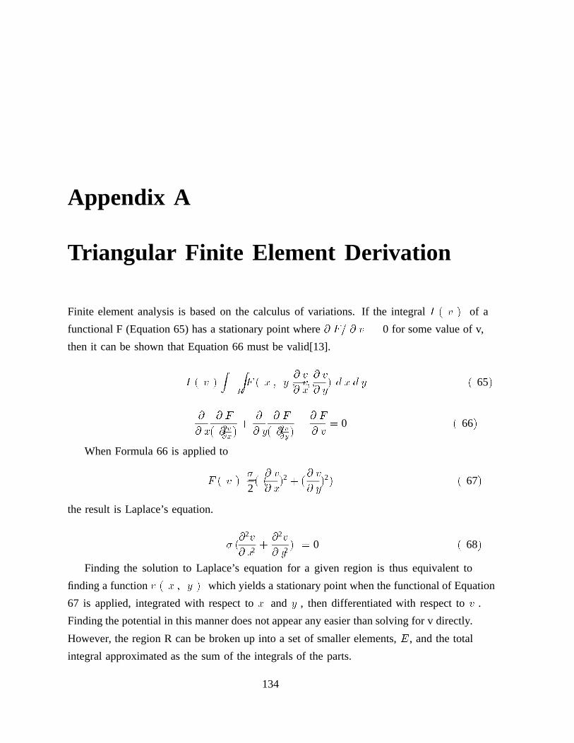
Appendix A
Triangular Finite Element Derivation
Finite element analysis is based on the calculus of variations. If the integralI ( v ) of a
functional F (Equation 65) has a stationary point where@ F= @ v = 0 for some value of v,
then it can be shown that Equation 66 must be valid[13].
I ( v ) =Z Z
RF ( x ; y ; v ;
@ v
@ x;@ v
@ y) d x d y ( 65)
@
@ x
@ F
( @@v@x)+
@
@ y
@ F
( @@v@y) @ F
@ v= 0 ( 66)
When Formula 66 is applied to
F ( v ) =
2( (@ v
@ x)2 + (
@ v
@ y)2) ( 67)
the result is Laplace’s equation.
(@2v
@ x2+@2v
@ y2) = 0 ( 68)
Finding the solution to Laplace’s equation for a given region is thus equivalent to
finding a functionv ( x ; y ) which yields a stationary point when the functional of Equation
67 is applied, integrated with respect tox and y , then differentiated with respect tov .
Finding the potential in this manner does not appear any easier than solving for v directly.
However, the region R can be broken up into a set of smaller elements,E, and the total
integral approximated as the sum of the integrals of the parts.
134
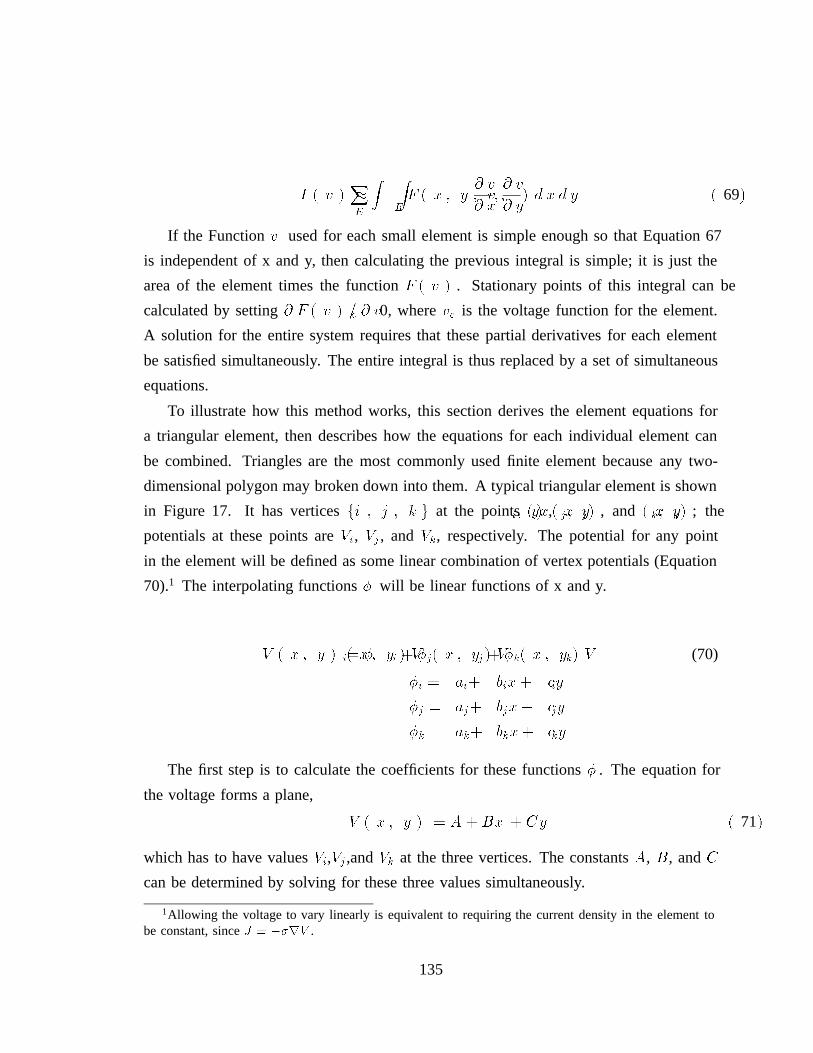
I ( v ) XE
Z ZEF ( x ; y ; v ;
@ v
@ x;@ v
@ y) d x d y ( 69)
If the Functionv used for each small element is simple enough so that Equation 67
is independent of x and y, then calculating the previous integral is simple; it is just the
area of the element times the functionF ( v ) . Stationary points of this integral can be
calculated by setting@ F ( v ) = @ ve = 0, whereve is the voltage function for the element.
A solution for the entire system requires that these partial derivatives for each element
be satisfied simultaneously. The entire integral is thus replaced by a set of simultaneous
equations.
To illustrate how this method works, this section derives the element equations for
a triangular element, then describes how the equations for each individual element can
be combined. Triangles are the most commonly used finite element because any two-
dimensional polygon may broken down into them. A typical triangular element is shown
in Figure 17. It has verticesfi ; j ; k g at the points( xi; yi) ,( xj ; yj) , and ( xk; yk) ; the
potentials at these points areVi, Vj , andVk, respectively. The potential for any point
in the element will be defined as some linear combination of vertex potentials (Equation
70).1 The interpolating functions will be linear functions of x and y.
V ( x ; y ) = i( x ; y ) Vi + j( x ; y ) Vj + k( x ; y ) Vk (70)
i = ai+ bix+ ciy
j = aj+ bjx+ cjy
k = ak+ bkx+ cky
The first step is to calculate the coefficients for these functions . The equation for
the voltage forms a plane,
V ( x ; y ) = A +Bx + Cy ( 71)
which has to have valuesVi,Vj ,andVk at the three vertices. The constantsA, B, andC
can be determined by solving for these three values simultaneously.
1Allowing the voltage to vary linearly is equivalent to requiring the current density in the element tobe constant, sinceJ = rV .
135
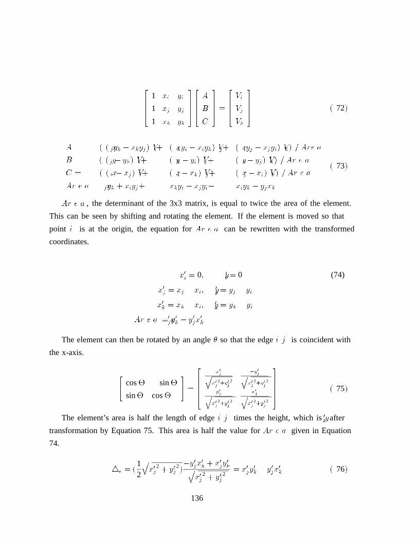
26664
1 xi yi
1 xj yj
1 xk yk
3777526664A
B
C
37775 =
26664Vi
Vj
Vk
37775 ( 72)
A = ( ( xjyk xkyj) Vi+ ( xkyi xiyk) Vj+ ( xiyj xjyi) Vk) = Are a
B = ( ( yj yk) Vi+ ( yk yi) Vj+ ( yi yj) Vk) = Ar e a
C = ( ( xk xj) Vi+ ( xi xk) Vj+ ( xj xi) Vk) = Ar e a
Ar e a = xjyk + xiyj+ xkyi xjyi xiyk yjxk
( 73)
Ar e a , the determinant of the 3x3 matrix, is equal to twice the area of the element.
This can be seen by shifting and rotating the element. If the element is moved so that
point i is at the origin, the equation forAr e a can be rewritten with the transformed
coordinates.
x0i = 0; y0i = 0 (74)
x0j = xj xi; y0j = yj yi
x0k = xk xi; y0k = yk yi
Ar e a = x0jy0
k y0jx0
k
The element can then be rotated by an angle so that the edgei j is coincident with
the x-axis.
24 cos sin
sin cos
35 =
266664
x0jqx0j
2+y0j
2
y0jqx0j
2+y0j
2
y0jqx0j
2+y0j2
x0jqx0j
2+y0j2
377775 ( 75)
The element’s area is half the length of edgei j times the height, which isy0k after
transformation by Equation 75. This area is half the value forAr e a given in Equation
74.
4e = (12
qx0j
2 + y0j2)y0jx0k + x0jy
0
kqx0j
2 + y0j2
= x0jy0
k y0jx0
k ( 76)
136
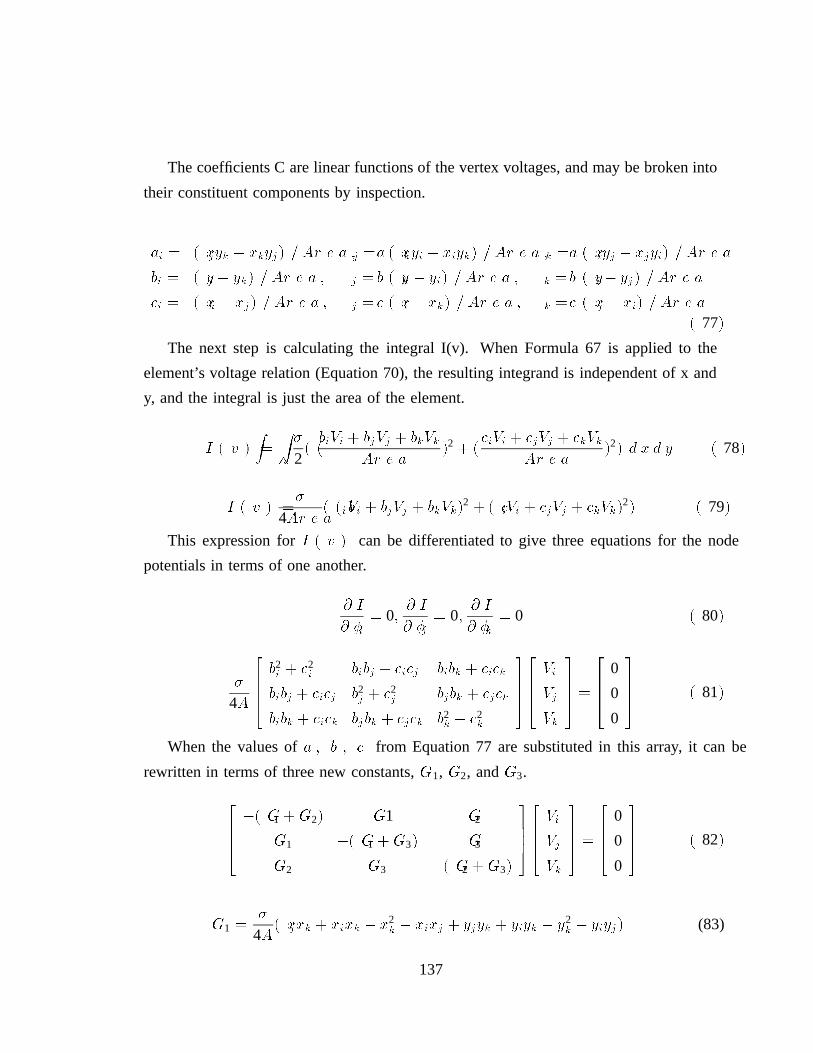
The coefficients C are linear functions of the vertex voltages, and may be broken into
their constituent components by inspection.
ai = ( xjyk xkyj) = Ar e a ; aj = ( xkyi xiyk) = Ar e a ; ak = ( xiyj xjyi) = Ar e a
bi = ( yj yk) = Ar e a ; bj = ( yk yi) = Ar e a ; bk = ( yi yj) = Ar e a
ci = ( xk xj) = Ar e a ; cj = ( xi xk) = Ar e a ; ck = ( xj xi) = Ar e a
( 77)
The next step is calculating the integral I(v). When Formula 67 is applied to the
element’s voltage relation (Equation 70), the resulting integrand is independent of x and
y, and the integral is just the area of the element.
I ( v ) =Z Z
4
2( (biVi + bjVj + bkVk
Ar e a)2 + (
ciVi + cjVj + ckVkAr e a
)2) d x d y ( 78)
I ( v ) =
4Ar e a( ( biVi + bjVj + bkVk)
2 + ( ciVi + cjVj + ckVk)2) ( 79)
This expression forI ( v ) can be differentiated to give three equations for the node
potentials in terms of one another.
@ I
@ i= 0;
@ I
@ j= 0;
@ I
@ k= 0 ( 80)
4A
26664b2i + c2
i bibj + cicj bibk + cick
bibj + cicj b2j + c2
j bjbk + cjck
bibk + cick bjbk + cjck b2k + c2
k
3777526664Vi
Vj
Vk
37775 =
26664
0
0
0
37775 ( 81)
When the values ofa ; b ; c from Equation 77 are substituted in this array, it can be
rewritten in terms of three new constants,G1, G2, andG3.
26664( G1 +G2) G1 G2
G1 ( G1 +G3) G3
G2 G3 ( G2 +G3)
3777526664Vi
Vj
Vk
37775 =
26664
0
0
0
37775 ( 82)
G1 =
4A( xjxk + xixk x2
k xixj + yjyk + yiyk y2k yiyj) (83)
137
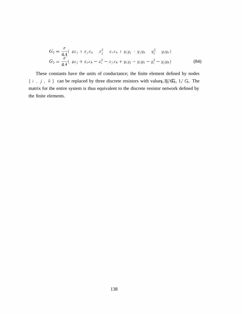
G2 =
4A( xixj + xjxk x2
j xixk + yiyj + yjyk y2j yiyk)
G3 =
4A( xixj + xixk x2
i xjxk + yiyj + yiyk y2i yjyk) (84)
These constants have the units of conductance; the finite element defined by nodes
f i ; j ; k g can be replaced by three discrete resistors with values 1= G1, 1= G2, 1= G3. The
matrix for the entire system is thus equivalent to the discrete resistor network defined by
the finite elements.
138

Bibliography
[1] Alfred Aho, John Hopcraft, and Jeffrey Ullman,The Design and Analysis of Computer Algo-
rithms, Addison-Wesley, Reading, Massachusetts, 1974, 172-176.
[2] Erich Barke, “Resistance Calculation From Mask Artwork Data by Finite Element Method”,
Proceedings of the 22nd Design Automation Conference,1985, 305-311.
[3] J.D. Bastian, M. Ellement, P.J. Fowler, C.E. Huang, and L. P. McNamee, “Symbolic Para-
sitic Extractor for Circuit Simulation (SPECS)”,Proceedings of the 20th Design Automation
Conference,1983, 346-352.
[4] F.H. Branin Jr., “The Analysis and Design of Power Distribution Nets on LSI chips”,Proceed-
ings of the International Conference on Circuits and Computers, 1980, 785-790.
[5] F.H. Branin Jr, and K. Huseyin,Problem Analysis in Science and Engineering, Academic Press,
New York, 1977, 56-66.
[6] R.E. Bryant, “A Switch-Level Model and Simulator for MOS Digital Systems”,IEEE Trans-
actions on Computers, Vol. C-33, No. 2, February 1984, pp. 160-177.
[7] R.E. Bryant, D. Beatty, K. Brace, K. Cho, and T. Sheffler, “COSMOS: A Compiled Simulator
For MOS Circuits”,Proceedings of the 24th Design Automation Conference,1987, pp 9-16.
[8] Basant R. Chawla and Hermann K. Gummel, “A Boundary Technique for Calculation of
Distributed Resistance”,IEEE Transactions on Electron Devices, Vol. ED-17, No. 10, October
1970, pp. 915-925.
[9] S. Chowdhury, “An Automated Design of Minimum-Area IC Power/Ground Nets”,Proceedings
of the 24th Design Automation Conference,1987, 223-229.
[10] S. Chowdhury and J.S. Barkatullah, “Estimation of Maximum Currents in MOS IC Logic
Circuits”, IEEE Transactions on Computer Aided Design,Vol. Cad-9, No. 6, June 1990, 642-
654.
139
[11] Paul Chow, editor.The MIPS-X RISC Microprocessor,Kluwer Academic Publishers, Norwell,
Massachusetts, 1989, p. 122.
[12] Chorng-Yeong Chu,Improved Models for Switch Level Simulation, Technical Report CSL-TR-
88-368, Stanford University, November 1988.
[13] R. Courant and D. Hilbert,Methods of Mathematical Physics, Interscience Publishers, New
York, 1953, 191-193.
[14] An-Chang Deng, Yan-Chyuan Shiau, and Kou-Hung Loh, “Time Domain Current Waveform
Simulation of CMOS Circuits”,1988 IEEE International Conference on Computer Aided De-
sign Digest of Technical Papers, 1988, 208-211.
[15] D. T. Fitzpatrick, “MEXTRA: A Manhattan Circuit Extractor”, Electronic Research Lab. Memo
M82/42, Electronics Research Laboratory, University of California, Berkeley, January, 1982.
[16] Alan George and Joseph W-H Liu,Computer Solution of Large Sparse Positive Definite Sys-
tems, Englewood Cliffs, Prentice Hall, 1981.
[17] Alan George, “Computer Implementation of the Finite Element Method”, Stanford Technical
Report STAN-CS-208, Stanford University, 1971.
[18] Alan George and Joseph W-H Liu, “An Implementation of a Peripheral Node Finder”,ACM
Transactions on Math Software 5, 1979, 286-295.
[19] Lance A. Glasser and Daniel W. Dobberpuhl,The Analysis and Design of VLSI Circuits,
133-134. Addison Wesley, 1985.
[20] P.M. Hall, “Resistance Calculations for Thin Film Patterns”,Thin Solid Films, Vol. 1, 1967/68,
pp. 277-295.
[21] Joseph E. Hall, Dale E. Hocevar, Ping Yang, and Michael J. McGraw, “SPIDER-A CAD
System for Modeling VLSI Metallization Patterns”,IEEE Transactions on Computer Aided
Design,Vol. Cad-6, No. 6, November 1987, 1023-1031.
[22] M. Glez Harbour and J. M. Drake, “Calculation of Multiterminal Resistances in Integrated
Circuits”, IEEE Transactions on Circuits and Systems,Vol CAS-33, No. 4, April 1986, 462-
465.
[23] Mark Alan Horowitz, Timing Models for MOS Circuits, Ph.D. Thesis, Stanford University,
1983.
140

[24] Mark Horowitz, Paul Chow, Don Stark, Richard T. Simoni, Arturo Salz, Steven Przybylski,
John Hennessy, Glenn Gulak, Anant Agarwal and John Acken, “MIPS-X: A 20-MIPS Peak,
32-bit Microprocessor with On-Chip Cache”,IEEE Journal of Solid State Circuits, Vol SC-22,
No. 5, October 1987, 790-799.
[25] Mark Horowitz and Robert W. Dutton, “Resistance Extraction from Mask Layout Data”,IEEE
Transactions on Computer Aided Design,Vol. Cad-2, No. 3, July 1983, 145-150.
[26] Norman P. Jouppi, “Derivation of Signal Flow Direction in MOS VLSI”,IEEE Transactions
on Computer Aided Design,Vol. Cad-6, No. 3, May 1987, 480-490.
[27] Norman P. Jouppi, “Timing Analysis and Performance Improvement of MOS VLSI Designs”,
IEEE Transactions on Computer Aided Design,Vol. Cad-6, No. 4, July 1987, 650-665.
[28] N. Jouppi, J. Tang, and J. Dion, “A 20 MIPS (Sustained) 32b CMOS Microprocessor with
64b Data Bus”,1989 IEEE International Solid State Circuits Conference Digest of Technical
Papers, 1989, 84-85.
[29] Russell Kao, Bob Alverson, Mark Horowitz and Don Stark, “Bisim: A Simulator for Cus-
tom ECL Circuits”,1988 IEEE International Conference on Computer Aided Design Digest of
Technical Papers, 1988, 62-65.
[30] Kuniyasu Kawarada, Masao Suzuki, Hisakazu Toyoda, and and Yoshisuke Kondo, “A Fast
7.5ns Access 1K-Bit RAM for Cache Memory Systems”,IEEE Journal of Solid State Circuits,
Vol SC-13, No. 5, October 1978, 656-663.
[31] Albertus J. Kemp, Jacobus A Pretorius, and Willem Smit, “The Generation of a Mesh for
Resistance Calculation in Integrated Circuits”,IEEE Transactions on Computer Aided Design,
Vol. Cad-7, No. 10, October 1988, 1029-1037.
[32] M.R. Lightner et al, “CSIM: The Evolution of a Behavioral Level Simulator from a Func-
tional Simulator: Implementation Issues and Performance Measurements”,Digest of Technical
Papers, 1985 IEEE International Conference on Computer-Aided Design, 350-352.
[33] Hu Ei Ling, “High-Speed Binary Adder”,IBM Journal of Research and Development, Vol. 25,
Nos. 2 and 3, May 1981, 156-166.
[34] Jorge Machek and Siegfried Selberherr, “A Novel Finite Element Approach to Device Mod-
elling”, IEEE Transactions on Electron Devices, Vol ED-30, No. 9, September 1983, 1083-
1091.
141

[35] Steven P. McCormick, “EXCL: A Circuit Extractor for IC Designs”,Proceedings of the 21st
Design Automation Conference,1984, 616-623.
[36] Takashi Mitsuhashi and Kenji Yoshida, “A Resistance Calculation Algorithm and Its Applica-
tion to Circuit Extraction”,IEEE Transactions on Computer Aided Design,Vol. Cad-6, No. 3,
May 1987, 337-345.
[37] Shojiro Mori and James A. Wilmore, “Resistance Extraction in a Hierarchical IC Artwork
Verification System”,Digest of Technical Papers, IEEE International Conference on Computer
Aided Design, 1985,196-198.
[38] Andrew S. Moulton, “Laying the Power and Ground Wires on a VLSI Chip”,Proceedings of
the 20th Design Automation Conference,1983, 754-755.
[39] L.W. Nagel, “SPICE2: A Computer Program to Simulate Semiconductor Circuits”, Memo-
randum No. ERL-M520, Electronics Research Laboratory, University of California, Berkeley,
1975.
[40] Farid Najm, Richard Burch, Ping Yang, and Ibrahim Hajj, “Crest - A Current Estimator for
CMOS Circuits”,1988 IEEE International Conference on Computer Aided Design Digest of
Technical Papers, 1988, 204-207.
[41] F.N. Najm, R. Burch, P. Yang, and I.N. Hajj, “Probabilistic Simulation for Reliability Analysis
of CMOS VLSI Circuits”, IEEE Transactions on Computer Aided Design,Vol. Cad-9, No. 4,
April 1990, 439-450.
[42] Zeev Nehari,Conformal Mapping, Dover Publications, New York, 1975, pp. 61-65.
[43] Yoshio Okamura, Yoshito Muraishi, Takashi Sato, and Yasuhiro Ikemoto, “LAS: Layout Pattern
Analysis System With New Approach”,Proceedings of the IEEE International Conference on
Circuits and Computers,1982, 308-311.
[44] John K. Ousterhout, Gordon T. Hamachi, Robert N. Mayo, Walter S. Scott, and George Taylor,
“Magic: A VLSI Layout System”,Proceedings of the 21st Design Automation Conference,
1984, 152-159.
[45] J.K. Ousterhout, “Corner Stitching: A Data-Structuring Technique for VLSI Layout Tools”,
IEEE Transactions on Computer Aided Design,Vol. Cad-3, No. 1, January 1984, 87-100.
[46] J.K. Ousterhout, “A switch-level timing verifier for digital MOS VLSI”,IEEE Transactions
on Computer Aided Design,Vol. Cad-4, No. 3, July 1985, 336-348.
142

[47] Tomoyuki Ozaki, Jun Yoshida, Masahiro Kosaka, “PANAMAP-1: A Mask Pattern Analysis
Program for IC/LSI – Centerline Extraction and Resistance Calculation –”,Proceedings of the
1980 International Symposium on Circuits and Systems,1979, 1020-1024.
[48] David Roberts, Tim Layman, and George Taylor, “An ECL RISC Microprocessor Designed
for Two Level Cache”,Compcon 1990 Proceedings, 1990, 228-231.
[49] H-J. Rothermel and D. A. Mlynski, “Computation of Power Supply Nets in VLSI Layout”,
Proceedings of the 18th Design Automation Conference,1981, 37-47.
[50] Jorge Rubenstein, Paul Penfield, Jr. and Mark A. Horowitz, “Signal Delay in RC Tree Net-
works”,IEEE Transactions on Computer Aided Design,Vol. Cad-2, No. 3, July 1983, 202-210.
[51] Mark Santoro and Mark Horowitz, “A Pipelined 64 x 64b Iterative Array Multiplier”,1988
IEEE International Solid State Circuits Conference Digest of Technical Papers, 1988, 36-37.
[52] Walter S. Scott and John K. Ousterhout, “Magic’s Circuit Extractor”,Proceedings of the 22nd
Design Automation Conference,1985, 286-292.
[53] Don Stark and Mark Horowitz, “REDS: Resistance Extraction for Use in Digital Simulation”,
Proceedings of the 24th Design Automation Conference,1987, 570-573.
[54] Don Stark and Mark Horowitz, “Analyzing Power Supply Networks Using Ariel”,Proceedings
of the 25th Design Automation Conference, 1988, 460-464.
[55] Shun Lin Su, Vasant B. Rao, and Timothy N. Trick, “HPEX: A Hierarchical Parasitic Circuit
Extractor”,Proceedings of the 24th Design Automation Conference,1987, 566-569.
[56] Zahir A. Syed and Abbas El Gamal, “Single Layer Routing for Power and Ground Networks
in Integrated Circuits”,Journal of Digital Systems, Vol. 6, No. 1, Spring 1982, 53-63.
[57] C. J. Terman,Simulation Tools for Digital LSI Design, Ph.D. Thesis, MIT Department of
Electrical Engineering and Computer Science, 1983.
[58] Akhilesh Tyagi,The Role of Energy in VLSI Computations, Technical Report 88-06-05, Uni-
versity of Washington, Seattle, June 1988.
[59] Harry J.M. Veendrick, “Short Circuit Dissipation of Static CMOS Circuitry and its Impact on
the Design of Buffer Circuits”,IEEE Journal of Solid State Circuits, Vol SC-19, No. 4, August
1984, 468-473.
143

[60] T.E. Williams, M. Horowitz, R. L. Alverson, and T.S. Yang, “A Self-Timed Chip for Divi-
sion”, Advanced Research in VLSI: Proceedings of the 1987 Stanford Conference, MIT Press,
Cambridge, 1987, 75-96.
[61] Hiroshi Yoshimura, Kazuo Tansho, Norihiko Ohwada, and Tadashi Nishide, “An Algorithm
for Resistance Calculation From IC Mask Pattern Information”,Proceedings of the 1979 In-
ternational Symposium on Circuits and Systems1979, 478-481.
144