analysis of impact of transistor aging...
TRANSCRIPT
ANALYSIS OF IMPACT OF TRANSISTOR AGING EFFECTS ON CLOCK SKEW
IN NANO-SCALE CMOS
A thesis work submitted to the faculty of
San Francisco State University
In partial fulfillment of
The Requirements for
The Degree
Master in Sciences
In
Engineering
by
Mandeep Singh Randhawa
San Francisco State University, California
May 2011

Copyright by
Mandeep Singh Randhawa
2011

CERTIFICATE OF APPROVAL
I certify that I have read Analysis of Clock Skew under combined effects of Transistor
Aging, Temperature and Capacitance mismatch in Nano-scale CMOS by Mandeep Singh
Randhawa, and in my opinion this work meets the criteria for approving a thesis
submitted in partial fulfillment of the requirement for degree: Master of Sciences in
Engineering at San Francisco State University.
_____________________________________________
Hamid Mahmoodi
Assistant Professor, Electrical and Computer Engineering
_____________________________________________
Hao Jiang
Professor, Electrical and Computer Engineering

ANALYSIS OF IMPACT OF TRANSISTOR AGING EFFECTS ON CLOCK SKEW
IN NANO-SCALE CMOS
Mandeep Singh Randhawa
2011
Transistor aging effects in Nano-scale CMOS result in transistor performance degradation over
the device life-time. The primary physical mechanism behind transistor aging is Bias
Temperature Instability (BTI). Such transistor aging results in circuit performance degradation
over time. In this research we are interested in analyzing the impact of the BTI aging effect on
clock skew in on-chip clock distribution networks. Clock skew is an important parameter in the
clock distribution. It is defined as the maximum time difference between the clock signals
received at different end points of a clock distribution network on a chip. The reason for clock
skew could be process variations, temperature, or capacitance differences across the clock
network. Ideally the clock signal has to be fully synchronous everywhere on a chip (i.e. clock
skew of zero), but in reality we get some limited clock skew in the order of a few Pico-Second. If
clock skew becomes too high, it can result in timing errors in synchronous designs. In this
research, we have analyzed and quantify the impact of transistor aging effects on clock skew. We
have simulated an H-tree clock distribution network and analyzed how the transistor aging affects
clock skew over a period of 2 years. Our results show that the Vt mismatch and low temperature
mismatch induced clock skew reduces as a result of transistor aging over time, whereas
capacitance mismatch and high temperature mismatch induced clock skew increases over time a
result of transistor aging. In a 32nm technology node, the clock skew aging could be in the range
of -26% to +36% depending on mismatch cause of clock skew.
I certify that the Abstract is a correct representation of the content of this thesis.
_____________________________ ___________
Chair, Thesis Committee Date

ACKNOWLEDGEMENTS
I would like to thanks my thesis advisor Dr. Hamid Mahmoodi for his invaluable
guidance and support towards the completion of my thesis. I would also take this
opportunity to thank my committee member Dr. Hao Jiang for his assistance. I am
grateful to the School of Engineering and the team of NECRL (Nano Electronics and
Computing Research Lab) for providing me with the necessary tools and other resources
required to complete this project. I would like thank my family members and friends for
their help and co-operation during my work.
vi

TABLE OF CONTENTS
Acknowledgements
1. Introduction……………………………………………….……......1
2. BTI Model……………………………………………….……..…..4
3. Aging of Clock skew under Vt Mismatch…………………...…......6
4. Aging of Clock Skew under Temperature Mismatch……..…....…..8
5. Aging of Clock Skew under Capacitance Mismatch….……..…....10
6. Realistic Temperature Profile…………………………….…..…...12
7. Conclusion…………………………………………………...…....14
8. References………………………………………………....……...15
vii

LIST OF FIGURES
Fig. 1 2-Level H-Tree
Fig. 2 Vt shift for three technology corners: Low Vt Transistors, Nominal Vt Transistors
and High Vt Transistors at room temperature (25°C) and worst case temperature (100°C)
Fig. 3 Clock Skew under the effect of Vt Mismatch
Fig. 4 Clock Skew under Temperature Mismatch
Fig. 5 Clock Skew under Capacitance Mismatch
Fig. 6 Temperature Profile of the Test Chip
Fig. 7 Clock Skew under Realistic Temperature Profile
viii

1
1. INTRODUCTION
Clock skew has emerged as a big performance limiting factor in sub 65nm technologies.
Its cause could be process variation, temperature mismatch or capacitance mismatch.
Moreover, due to transistor aging effects in Nano-scale, circuit delay will increase over
lifetime. Aging also impacts the clock skew over lifetime.
Aging effect has become a critical issue as the size of transistors is scaling down.
Bias Temperature Instability (BTI) effect can be further divided into NBTI and PBTI.
NBTI effect degrades the performance of PMOS over time by increasing its threshold
voltage. Similarly PBTI effect degrades the performance of NMOS. As the use of High K
materials is increasing; PBTI effect is also increasing. In [5] and [6], authors have
discussed how variability in process, temperature and power fluctuation could affect
clock skew, whereas in our work we have incorporated the effect of aging along with
temperature and capacitance mismatch. This is the first paper which has incorporated the
effects of temperature and capacitance mismatch along with aging effects. We also used
realistic temperature profile of a chip [3]; to calculate the effect of aging and performed
simulations to obtain clock skew results over the 2-year period.
In this research we have simulated an H- tree clock distribution network in a
predictive 32 nm technology [1]. The clock distributions network is a two-level H-tree as
shown in Fig. 1. There is one H tree in the first level and 4 H-trees in the second level. A
single H-tree has 6 buffers; therefore there are 30 buffers in the entire H-tree network.
The buffers used in this H-tree network are CMOS inverters made using PMOS and
NMOS transistors. The second level H-trees are situated at the four end nodes of the first
level H-tree; they receive input from the end nodes of the first level H tree.

2
Fig. 1: 2-Level H-Tree
The contributions in this work are as follows:
We have performed an analysis of combined effect of NBTI and PBTI on clock
skew
We have performed the clock skew aging analysis under Vt, temperature, and
capacitive mismatch.
L-Tree R-Tree

3
We show that the clock skew reduces by transistor aging when the cause of
mismatch is Vt or low temperature difference. We show that the clock skew
increases by transistor aging when the cause of mismatch is capacitance or high
temperature difference.
We have performed clock skew aging analysis using a realistic temperature
profile of a test chip.
4
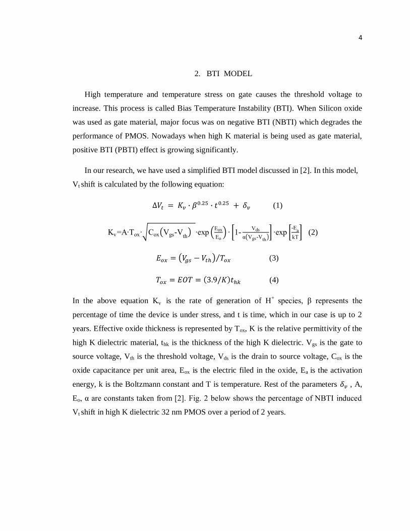
2. BTI MODEL
High temperature and temperature stress on gate causes the threshold voltage to
increase. This process is called Bias Temperature Instability (BTI). When Silicon oxide
was used as gate material, major focus was on negative BTI (NBTI) which degrades the
performance of PMOS. Nowadays when high K material is being used as gate material,
positive BTI (PBTI) effect is growing significantly.
In our research, we have used a simplified BTI model discussed in [2]. In this model,
Vt shift is calculated by the following equation:
(1)
To o g - h e p
o
o -
d
g - h e p
-
T (2)
(3)
(4)
In the above equation is the rate of generation of H+ pecie , β repre en he
percentage of time the device is under stress, and t is time, which in our case is up to 2
years. Effective oxide thickness is represented by Tox, K is the relative permittivity of the
high K dielectric material, thk is the thickness of the high K dielectric. Vgs is the gate to
source voltage, Vth is the threshold voltage, Vds is the drain to source voltage, Cox is the
oxide capacitance per unit area, Eox is the electric filed in the oxide, Ea is the activation
energy, k is the Boltzmann constant and T is temperature. Rest of the parameters , A,
Eo, re con n en from [2]. Fig. 2 below how he percen ge of NBTI induced
Vt shift in high K dielectric 32 nm PMOS over a period of 2 years.

5
Fig. 2: Percentage of NBTI induced Vt shift in high K dielectric 32 nm PMOS
6
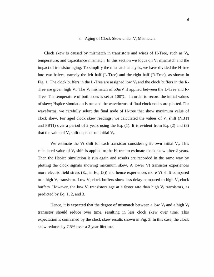
3. Aging of Clock Skew under Vt Mismatch
Clock skew is caused by mismatch in transistors and wires of H-Tree, such as Vt,
temperature, and capacitance mismatch. In this section we focus on Vt mismatch and the
impact of transistor aging. To simplify the mismatch analysis, we have divided the H-tree
into two halves; namely the left half (L-Tree) and the right half (R-Tree), as shown in
Fig. 1. The clock buffers in the L-Tree are assigned low Vt and the clock buffers in the R-
Tree are given high Vt. The Vt mismatch of 50mV if applied between the L-Tree and R-
Tree. The temperature of both sides is set at 100°C. In order to record the initial values
of skew; Hspice simulation is run and the waveforms of final clock nodes are plotted. For
waveforms, we carefully select the final node of H-tree that show maximum value of
clock skew. For aged clock skew readings; we calculated the values of Vt shift (NBTI
and PBTI) over a period of 2 years using the Eq. (1). It is evident from Eq. (2) and (3)
that the value of Vt shift depends on initial Vt.
We estimate the Vt shift for each transistor considering its own initial Vt. This
calculated value of Vt shift is applied to the H–tree to estimate clock skew after 2 years.
Then the Hspice simulation is run again and results are recorded in the same way by
plotting the clock signals showing maximum skew. A lower Vt transistor experiences
more electric field stress (Eox in Eq. (3)) and hence experiences more Vt shift compared
to a high Vt transistor. Low Vt clock buffers show less delay compared to high Vt clock
buffers. However, the low Vt transistors age at a faster rate than high Vt transistors, as
predicted by Eq. 1, 2, and 3.
Hence, it is expected that the degree of mismatch between a low Vt and a high Vt
transistor should reduce over time, resulting in less clock skew over time. This
expectation is confirmed by the clock skew results shown in Fig. 3. In this case, the clock
skew reduces by 7.5% over a 2-year lifetime.

7
Fig. 3: Aging of clock skew with 50mV initial Vt mismatch
260.16
240.67
230
235
240
245
250
255
260
265
0 2
Clo
ck S
ke
w i
n p
s
Years
Clock Skew under Vt Mismatch
7.5%

8
4. Aging of Clock Skew under Temperature Mismatch
In this section we focus on temperature mismatch and the impact of transistor aging.
The L-Tree is assigned lower temperature and the R-Tree is assigned higher temperature.
The temperature mismatches we have applied are +/- 10, +/-20 and +/-30 °C. The chip
temperature in case of 10 °C mismatch is set at 100 °C and therefore +/- 10 °C will
correspond to 110 and 90 °C respectively. The assigned chip temperature for 20 °C
mismatch is set at 90 °C. Hence, +/- 20 mismatches will correspond to 110 and 70 °C
respectively. For 30 °C mismatch, chip temperature is set at 80 °C and +/- 30 is used to
assign the temperature of 50 °C to L-Tree side and 110 °C to R-Tree side of the H-tree.
Temperature has a strong influence on the aging. The rate of aging is higher at higher
temperatures as predicted by Eq. (2). We estimate the Vt shift for each transistor
considering its own operating temperature.
It is observed that the clock skew increases by transistor aging under large
temperature mismatch (20 and 30 °C). The increase in clock skew over a 2-year period is
36% and 18.3%, for the 20 and 30 °C mismatch cases, respectively. The increased clock
skew is due to uneven aging of the transistors in the L-Tree and R-Tree because of having
different operating temperature. However, under low temperature mismatch of 10 °C, the
clock skew reduces over the 2 year lifetime by 26%. This is due to the fact that higher
temperature lowers Vt but increases the rate of Vt increase caused by aging. For low
temperature mismatch, the difference in the rate of Vt shift between the L-Tree and R-
Tree results in a more balanced propagation delay through the H-tree over time, causing
clock skew reduction. This effect is not observed when the temperature mismatch is too
much. Fig. 4 shows the results of the above mentioned simulations.

9
Fig 4: Aging of clock skew with 10, 20 and 30 °C temperature mismatch over a period of
2 years.
10
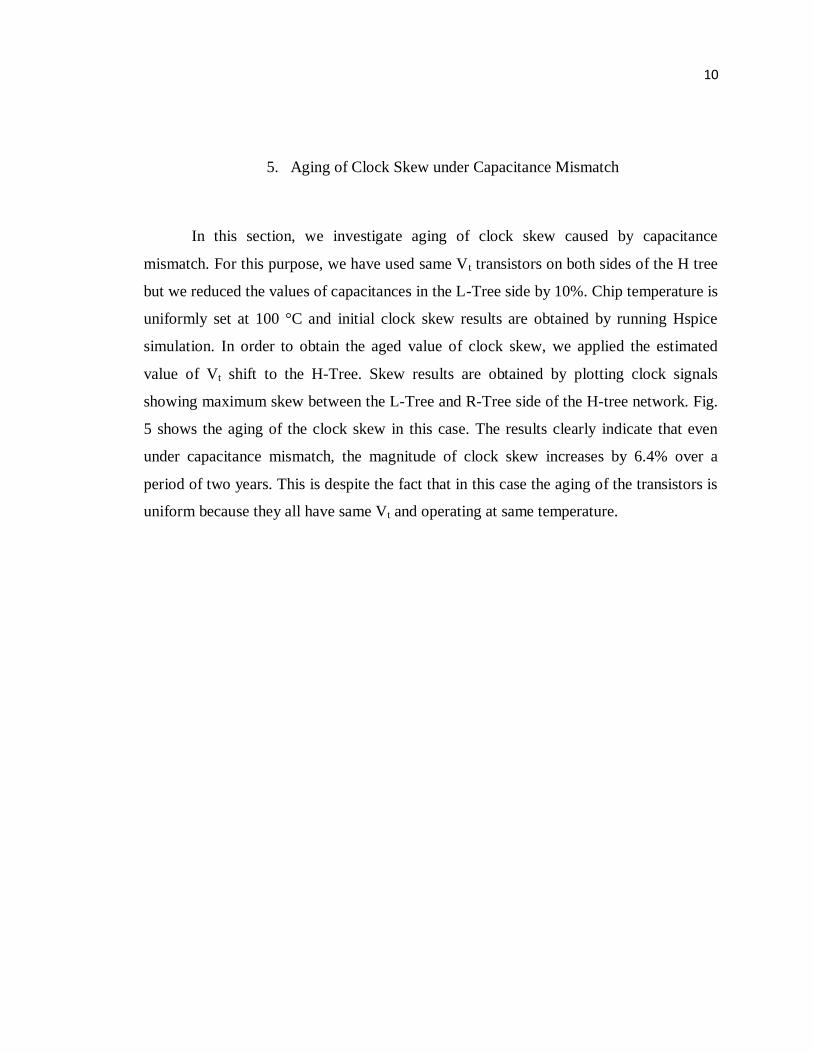
5. Aging of Clock Skew under Capacitance Mismatch
In this section, we investigate aging of clock skew caused by capacitance
mismatch. For this purpose, we have used same Vt transistors on both sides of the H tree
but we reduced the values of capacitances in the L-Tree side by 10%. Chip temperature is
uniformly set at 100 °C and initial clock skew results are obtained by running Hspice
simulation. In order to obtain the aged value of clock skew, we applied the estimated
value of Vt shift to the H-Tree. Skew results are obtained by plotting clock signals
showing maximum skew between the L-Tree and R-Tree side of the H-tree network. Fig.
5 shows the aging of the clock skew in this case. The results clearly indicate that even
under capacitance mismatch, the magnitude of clock skew increases by 6.4% over a
period of two years. This is despite the fact that in this case the aging of the transistors is
uniform because they all have same Vt and operating at same temperature.

11
Fig. 5: Aging of clock skew with 10% capacitance mismatch.
76.672
81.632
74
75
76
77
78
79
80
81
82
83
0 2
Clo
ck S
kew
in p
s
Time (Years)
Clock skew under capacitance mismatch
6.4%

12
6. Aging of Clock Skew under Realistic Temperature Profile
In order to consider more realistic mismatch scenarios, we have used the
temperature profile of a chip as discussed in [3] and applied it to our H-tree network. Fig.
6 shows the spatial temperature profile used for this study. All transistors are given same
Vt.
Fig. 6: Realistic chip temperature profile

13
In this case, every clock buffer in the H-tree is assigned a unique temperature
obtained from the spatial temperature profile. Moreover, since each clock buffer is at a
different temperature, the aging of each buffer will be different. The aging induced Vt
shift is strongly temperature dependent as modeled by Eq. (2). We estimate the Vt shift of
each transistor considering its own operating temperature. The initial clock skew is
obtained by plotting waveforms from all the 16 end nodes of the H-tree and measuring
the maximum skew. Then, the calculated values of Vt shift for 2-year lifetime are applied
to individual buffers of the H-tree. Aged clock skew result is obtained by plotting 16
waveforms from all the end nodes of H tree network and measuring maximum skew. Fig.
7 below shows the increase in clock skew over a period of 2 years. The results indicate a
significant increase of 18.68% over the period of 2 years. The results show that the aging
increases the clock skew significantly.
Fig. 7: Clock skew aging under realistic temperature profile.
135.28
160.56
120
125
130
135
140
145
150
155
160
165
0 2
Clo
ck S
kew
in p
s
Time (Years)
Clock Skew Under Realistic Temperature Profile
18.68%

14
7. CONCLUSION
In this research, we have analyzed how the magnitude clock skew varies under
transistor aging effects over a period of 2 years. We have analyzed the clock skew aging
under different scenarios of mismatch. It is observed that Vt mismatch and low-
temperature mismatch induced clock skew reduced by transistor aging whereas the high
temperature mismatch and capacitance mismatch induced clock skew increases over time
by transistors aging. We have applied a realistic temperature profile of a chip into our
clock tree and measured clock skew aging by applying aging to the clock buffers
depending on their individual operating temperatures. The results show that clock skew is
increasing over a period of two years. Results indicate that the best way to manage clock
skew under transistor aging is to achieve a more uniform temperature profile for the chip.
Under low temperature mismatch, it is possible that the clock skew may even reduce over
lifetime.

15
8. REFERENCES
[1] Predictive Technology Models: http://ptm.asu.edu
[2] R. i ond , W. W ng, Y. . o, “Modeling nd minimiz ion of PMOS NBTI
effec for robu n nome er de ign,” Design Automation Conference, 2006 43rd
ACM/IEEE , vol., no., pp.1047-1052.
[3] Pei-Yu Huang, Chih-Kang Lin, Yu-Min Lee, Nat. Chiao Tung Univ.,
H inchu, T iw n “Full chip herm l n ly i for e rly de ign ge i Gener lized
In egr l Tr n form ” Design Automation Conference, 2008. ASPDAC 2008, Asia
and South Pacific.
[4] Pullela, S. Menezes, N. Omar, J. Pillage, L.T. “S ew nd del y op imiz ion for
reli ble buffered cloc ree ” Computer-Aided Design, 1993. ICCAD-93, Digest of
Technical Papers, 1993 IEEE/ACM International Conference 1993.
[5] Hashimoto, M. Yamamoto, T. Onodera, H. Dept. of Communication & Computer
Eng., Kyoto Univ., Japan “S i ic l n ly i of cloc ew ri ion in H-tree
ruc ure” Quality of Electronic Design, 2005. ISQED 2005, Sixth International
Symposium 2005.
[6] Narasimhan, Ashok; Sridhar, Ramalingam; Dept. of Computer Sci. & Eng.,
Buffalo Univ., NY “Imp c of ri bili y on loc S ew in H- ree loc Ne wor ”
Quality Electronic Design, 2007, ISQED '07, 8th International Symposium 2007.