analog-to-digital audio conversion example using stm32l4 … · analog-to-digital audio conversion...
TRANSCRIPT

June 2017 DocID030334 Rev 1 1/38
1
AN5012Application note
Analog-to-digital audio conversion example using STM32L4 Series microcontroller peripherals
Introduction
The purpose of this application note is to provide an analog-to-digital audio conversion example using the STM32L4 Series microcontroller peripherals (OPAMP, ADC and the Full-Speed USB).
This example uses the ADC dedicated features to improve the conversion resolution and to automatically detect a programmable threshold level.
Note that the values provided in this application note are for reference only, measured in a laboratory under typical conditions (unless otherwise specified) and not tested in production.
www.st.com
Contents AN5012
2/38 DocID030334 Rev 1
Contents
1 The principle of an audio signal capture . . . . . . . . . . . . . . . . . . . . . . . . 6
1.1 Audio signal characteristics . . . . . . . . . . . . . . . . . . . . . . . . . . . . . . . . . . . . 6
2 Analog to Digital Converter (ADC) operating mode . . . . . . . . . . . . . . . . 7
2.1 Principle . . . . . . . . . . . . . . . . . . . . . . . . . . . . . . . . . . . . . . . . . . . . . . . . . . . 7
2.2 STM32L4 ADC electrical circuitry network . . . . . . . . . . . . . . . . . . . . . . . . . 8
2.3 DC adapting network . . . . . . . . . . . . . . . . . . . . . . . . . . . . . . . . . . . . . . . . . 8
2.4 Gain of the pre-amplifier stage . . . . . . . . . . . . . . . . . . . . . . . . . . . . . . . . . . 9
2.5 Anti-alias filter . . . . . . . . . . . . . . . . . . . . . . . . . . . . . . . . . . . . . . . . . . . . . . . 9
2.6 Schematic using an STM32L4 internal OPAMP . . . . . . . . . . . . . . . . . . . . 10
3 Implementation with the STM32L4 Series microcontroller . . . . . . . . . 11
3.1 Overview of the project architecture . . . . . . . . . . . . . . . . . . . . . . . . . . . . . .11
3.2 Architecture of the firmware . . . . . . . . . . . . . . . . . . . . . . . . . . . . . . . . . . . 14
3.3 Architecture of the clock tree . . . . . . . . . . . . . . . . . . . . . . . . . . . . . . . . . . 16
3.3.1 Architecture presentation . . . . . . . . . . . . . . . . . . . . . . . . . . . . . . . . . . . . 16
3.3.2 Clocks constraints and relationship . . . . . . . . . . . . . . . . . . . . . . . . . . . 17
3.3.3 USB peripheral clocking . . . . . . . . . . . . . . . . . . . . . . . . . . . . . . . . . . . . 18
3.4 Data format (numeric domain) . . . . . . . . . . . . . . . . . . . . . . . . . . . . . . . . . 19
4 Application . . . . . . . . . . . . . . . . . . . . . . . . . . . . . . . . . . . . . . . . . . . . . . . . 21
4.1 Simple voice detection using ADC watchdog feature . . . . . . . . . . . . . . . . 21
5 Audio measurements definition . . . . . . . . . . . . . . . . . . . . . . . . . . . . . . . 23
5.1 Offset measurement . . . . . . . . . . . . . . . . . . . . . . . . . . . . . . . . . . . . . . . . . 23
5.2 Frequency response measurement . . . . . . . . . . . . . . . . . . . . . . . . . . . . . 23
5.3 Dynamic-range measurement . . . . . . . . . . . . . . . . . . . . . . . . . . . . . . . . . 23
5.4 Total Harmonic Distortion . . . . . . . . . . . . . . . . . . . . . . . . . . . . . . . . . . . . . 23
6 Signal acquisition measurements . . . . . . . . . . . . . . . . . . . . . . . . . . . . . 24
6.1 Spectrums . . . . . . . . . . . . . . . . . . . . . . . . . . . . . . . . . . . . . . . . . . . . . . . . 25
6.2 Level variation versus frequency . . . . . . . . . . . . . . . . . . . . . . . . . . . . . . . 27
6.3 THD+N variation versus level . . . . . . . . . . . . . . . . . . . . . . . . . . . . . . . . . . 28
DocID030334 Rev 1 3/38
AN5012 Contents
3
6.4 THD variation versus level . . . . . . . . . . . . . . . . . . . . . . . . . . . . . . . . . . . . 28
6.5 SINAD variation versus level . . . . . . . . . . . . . . . . . . . . . . . . . . . . . . . . . . 29
6.6 Measurement summary . . . . . . . . . . . . . . . . . . . . . . . . . . . . . . . . . . . . . . 30
6.7 Power consumption . . . . . . . . . . . . . . . . . . . . . . . . . . . . . . . . . . . . . . . . . 30
7 Measurement conclusions . . . . . . . . . . . . . . . . . . . . . . . . . . . . . . . . . . 31
Appendix A Data format from ADC to USB device (uint32_t to int16_t type) . . 32
Appendix B Octave script . . . . . . . . . . . . . . . . . . . . . . . . . . . . . . . . . . . . . . . . . . . 33
Appendix C ADC peripheral configuration function . . . . . . . . . . . . . . . . . . . . . . 35
Revision history . . . . . . . . . . . . . . . . . . . . . . . . . . . . . . . . . . . . . . . . . . . . . . . . . . . . 37
List of tables AN5012
4/38 DocID030334 Rev 1
List of tables
Table 1. ADC dynamic range . . . . . . . . . . . . . . . . . . . . . . . . . . . . . . . . . . . . . . . . . . . . . . . . . . . . . . . 9Table 2. ADC clock frequency range versus OSR and clock cycle (48 kHz) . . . . . . . . . . . . . . . . . . 17Table 3. Measurement summary . . . . . . . . . . . . . . . . . . . . . . . . . . . . . . . . . . . . . . . . . . . . . . . . . . . 30Table 4. Document revision history . . . . . . . . . . . . . . . . . . . . . . . . . . . . . . . . . . . . . . . . . . . . . . . . . 37
DocID030334 Rev 1 5/38
AN5012 List of figures
5
List of figures
Figure 1. Microphone sound pressure level and sensitivity . . . . . . . . . . . . . . . . . . . . . . . . . . . . . . . . . 6Figure 2. ADC behavior . . . . . . . . . . . . . . . . . . . . . . . . . . . . . . . . . . . . . . . . . . . . . . . . . . . . . . . . . . . . 7Figure 3. DC biasing . . . . . . . . . . . . . . . . . . . . . . . . . . . . . . . . . . . . . . . . . . . . . . . . . . . . . . . . . . . . . . 8Figure 4. High-pass filter schematic. . . . . . . . . . . . . . . . . . . . . . . . . . . . . . . . . . . . . . . . . . . . . . . . . . . 8Figure 5. Microphone to OPAMP interface schematic . . . . . . . . . . . . . . . . . . . . . . . . . . . . . . . . . . . . 10Figure 6. Hardware overview . . . . . . . . . . . . . . . . . . . . . . . . . . . . . . . . . . . . . . . . . . . . . . . . . . . . . . . 11Figure 7. Stack board with audio analyzer . . . . . . . . . . . . . . . . . . . . . . . . . . . . . . . . . . . . . . . . . . . . . 12Figure 8. Microphone recording . . . . . . . . . . . . . . . . . . . . . . . . . . . . . . . . . . . . . . . . . . . . . . . . . . . . . 13Figure 9. Firmware content . . . . . . . . . . . . . . . . . . . . . . . . . . . . . . . . . . . . . . . . . . . . . . . . . . . . . . . . 14Figure 10. DMA data exchange between ADC and US peripherals . . . . . . . . . . . . . . . . . . . . . . . . . . 15Figure 11. CubeMX default configuration . . . . . . . . . . . . . . . . . . . . . . . . . . . . . . . . . . . . . . . . . . . . . . 16Figure 12. ADC/DMA data exchange mechanism . . . . . . . . . . . . . . . . . . . . . . . . . . . . . . . . . . . . . . . . 18Figure 13. Word representation: unsigned integer (bits) . . . . . . . . . . . . . . . . . . . . . . . . . . . . . . . . . . . 19Figure 14. Word representation: unsigned integer (bits) . . . . . . . . . . . . . . . . . . . . . . . . . . . . . . . . . . . 19Figure 15. Word representation: signed integer (bits) . . . . . . . . . . . . . . . . . . . . . . . . . . . . . . . . . . . . . 19Figure 16. STM32 ADC acquisition - 48000 Hz . . . . . . . . . . . . . . . . . . . . . . . . . . . . . . . . . . . . . . . . . . 20Figure 17. Audio and ADC analog watchdog (threshold +/- 128) . . . . . . . . . . . . . . . . . . . . . . . . . . . . 21Figure 18. ADC code window . . . . . . . . . . . . . . . . . . . . . . . . . . . . . . . . . . . . . . . . . . . . . . . . . . . . . . . 22Figure 19. Spectrum plot: output signal level - 6 dBFS / Frequency 1 kHz . . . . . . . . . . . . . . . . . . . . . 25Figure 20. Spectrum plot: output signal level - 46 dBFS / Frequency 1 kHz . . . . . . . . . . . . . . . . . . . . 26Figure 21. Level variation versus frequency (-3 dB cut-off frequency reached at 17.8 kHz) . . . . . . . . 27Figure 22. THD+N variation . . . . . . . . . . . . . . . . . . . . . . . . . . . . . . . . . . . . . . . . . . . . . . . . . . . . . . . . . 28Figure 23. THD variation . . . . . . . . . . . . . . . . . . . . . . . . . . . . . . . . . . . . . . . . . . . . . . . . . . . . . . . . . . . 28Figure 24. SINAD variation . . . . . . . . . . . . . . . . . . . . . . . . . . . . . . . . . . . . . . . . . . . . . . . . . . . . . . . . . 29Figure 25. Power consumption . . . . . . . . . . . . . . . . . . . . . . . . . . . . . . . . . . . . . . . . . . . . . . . . . . . . . . 30Figure 26. Average power consumption . . . . . . . . . . . . . . . . . . . . . . . . . . . . . . . . . . . . . . . . . . . . . . . 30
The principle of an audio signal capture AN5012
6/38 DocID030334 Rev 1
1 The principle of an audio signal capture
1.1 Audio signal characteristics
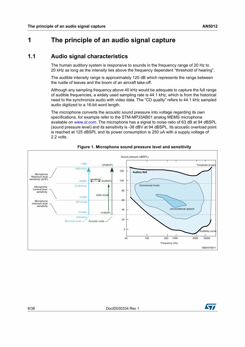
The human auditory system is responsive to sounds in the frequency range of 20 Hz to 20 kHz as long as the intensity lies above the frequency dependent “threshold of hearing”.
The audible intensity range is approximately 120 dB which represents the range between the rustle of leaves and the boom of an aircraft take-off.
Although any sampling frequency above 40 kHz would be adequate to capture the full range of audible frequencies, a widely used sampling rate is 44.1 kHz, which is from the historical need to the synchronize audio with video data. The “CD quality” refers to 44.1 kHz sampled audio digitized to a 16-bit word length.
The microphone converts the acoustic sound pressure into voltage regarding its own specifications, for example refer to the STM-MP33AB01 analog MEMS microphone available on www.st.com. The microphone has a signal to noise ratio of 63 dB at 94 dBSPL (sound pressure level) and its sensitivity is -38 dBV at 94 dBSPL. Its acoustic overload point is reached at 125 dBSPL and its power consumption is 250 uA with a supply voltage of 2.2 volts.
Figure 1. Microphone sound pressure level and sensitivity
DocID030334 Rev 1 7/38
AN5012 Analog to Digital Converter (ADC) operating mode
37
2 Analog to Digital Converter (ADC) operating mode
2.1 Principle
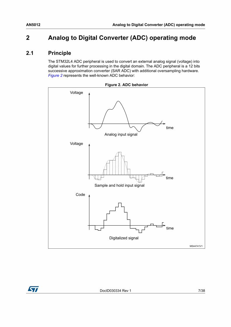
The STM32L4 ADC peripheral is used to convert an external analog signal (voltage) into digital values for further processing in the digital domain. The ADC peripheral is a 12 bits successive approximation converter (SAR ADC) with additional oversampling hardware. Figure 2 represents the well-known ADC behavior:
Figure 2. ADC behavior

Analog to Digital Converter (ADC) operating mode AN5012
8/38 DocID030334 Rev 1
2.2 STM32L4 ADC electrical circuitry network
The STM32L4 SAR ADC has a fixed input architecture which can be single-end or differential. If the application is using an analog microphone, a signal scaling with few external components is required.
2.3 DC adapting network
The STM32L4 ADC converts the input analog signal in voltage range 0 V to 1.62 V/3.6 V (VDDA supply). Because the microphone audio signal is centered on ground, a specific electrical schematic is required to adapt the common voltage mode from 0 V to VDDA/2, as shown in Figure 3 and Figure 4.
Figure 3. DC biasing
This signal adaptation is performed using the following schematic (high-pass filter):
Figure 4. High-pass filter schematic
DocID030334 Rev 1 9/38
AN5012 Analog to Digital Converter (ADC) operating mode
37
2.4 Gain of the pre-amplifier stage
The output level of the analog microphone is very small regarding the resolution of the ADC converter. The signal must be amplified correctly to fit with the input range of the converter. Here below a comparison is done of the analog signal level with and without gain.
Without amplification, the acquired audio signal corresponding to 60 dBSPL sound pressure has an equivalent electrical level (RMS) of 251 uV or -72 dBV (see Figure 1).
The less significant bit (LSB) represents the minimum voltage that can be converted. Using the STM32L4 ADC with the lowest voltage for VDDA (1.65 V), its value can be calculated using the following formula:
LSB = VDDA/2Nb bits ADC
LSB = 1.65 V/4096 = 402.8 uV
Note: This LSB level is greater than 251 uV coming from the microphone.
The signal coming from the microphone must be amplified using either an external amplifier or the STM32L4 build-in OPAMP.
With an amplification of 24 dB (internal amplification with the OPAMP peripheral), the amplified electrical signal has an amplitude of 4 mV or -48 dBV:
ADC input signal = Microphone signal x Amplifier gain = (251.10-6) x 10(24/20)
= (251.10-6) x 15.85 = 4.10-3 = 4 mV or 20 x log10(4.10-3) = -48 dBV
Using the STM32L4 ADC with VDDA = 3.3 V and an over sampling ratio of 64, Table 1 shows the ADC output amplitude obtained in the numeric domain (ADC LSB = VDDA/2Nb bits ADC).
The dynamic range is the ratio between the maximum and the minimum signal level (0 lsb is the minimum level while the maximum level depends on the gain in the acquisition path).
2.5 Anti-alias filter
Because the ADC converter is sampling and holding the input signal to avoid any folding/aliasing effect, the signal should not change during the sample acquisition duration and a simple low-pass filter (last stage) may be added in order to attenuate the signal above the Nyquist–Shannon sampling frequency (FsADC/2).
In this application example, a first order low-pass filter is used with R=5 kΩ and C=1 nF. Its cut-off frequency (Fc) is equal to 31.8 kHz and the attenuation at 20 kHz (calculated) is -1.44 dB.
Table 1. ADC dynamic range
Parameter Audio Source Gain ADC input level ADC output level Dynamic range
Units dBSPL dB mVrms mVpp FS with OSR =64 dB
Value 60 24 4 11.31 898 59
Analog to Digital Converter (ADC) operating mode AN5012
10/38 DocID030334 Rev 1
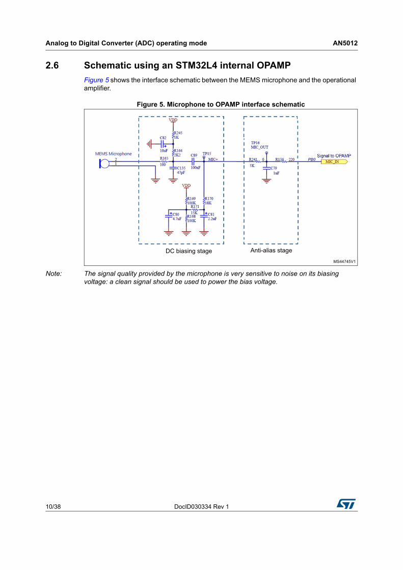
2.6 Schematic using an STM32L4 internal OPAMP
Figure 5 shows the interface schematic between the MEMS microphone and the operational amplifier.
Figure 5. Microphone to OPAMP interface schematic
Note: The signal quality provided by the microphone is very sensitive to noise on its biasing voltage: a clean signal should be used to power the bias voltage.
DocID030334 Rev 1 11/38
AN5012 Implementation with the STM32L4 Series microcontroller
37
3 Implementation with the STM32L4 Series microcontroller
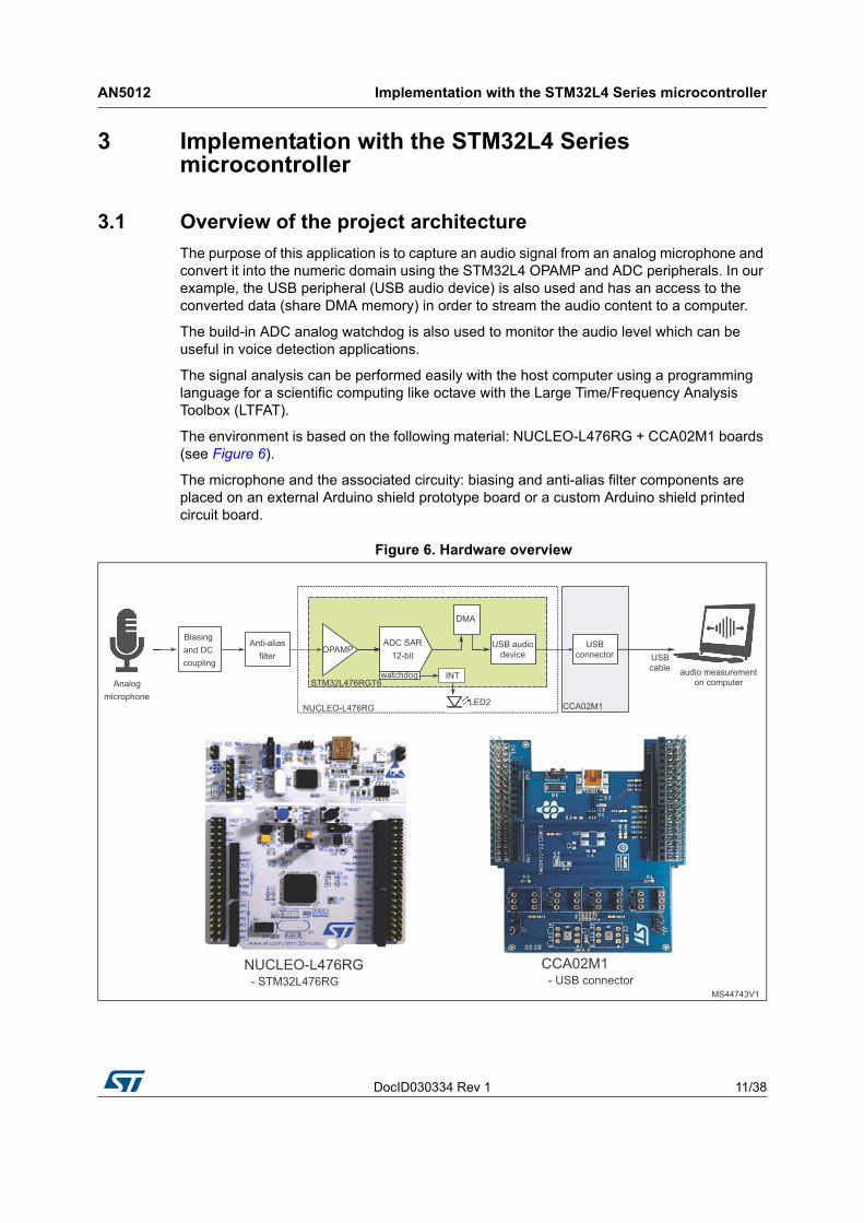
3.1 Overview of the project architecture
The purpose of this application is to capture an audio signal from an analog microphone and convert it into the numeric domain using the STM32L4 OPAMP and ADC peripherals. In our example, the USB peripheral (USB audio device) is also used and has an access to the converted data (share DMA memory) in order to stream the audio content to a computer.
The build-in ADC analog watchdog is also used to monitor the audio level which can be useful in voice detection applications.
The signal analysis can be performed easily with the host computer using a programming language for a scientific computing like octave with the Large Time/Frequency Analysis Toolbox (LTFAT).
The environment is based on the following material: NUCLEO-L476RG + CCA02M1 boards (see Figure 6).
The microphone and the associated circuity: biasing and anti-alias filter components are placed on an external Arduino shield prototype board or a custom Arduino shield printed circuit board.
Figure 6. Hardware overview

Implementation with the STM32L4 Series microcontroller AN5012
12/38 DocID030334 Rev 1
Figure 7 presents the stack board with the audio analyzer.
Figure 7. Stack board with audio analyzer

DocID030334 Rev 1 13/38
AN5012 Implementation with the STM32L4 Series microcontroller
37
The USB audio device is available under Windows 7 operating system as a stereo recording device, as shown on Figure 8.
Figure 8. Microphone recording
Implementation with the STM32L4 Series microcontroller AN5012
14/38 DocID030334 Rev 1
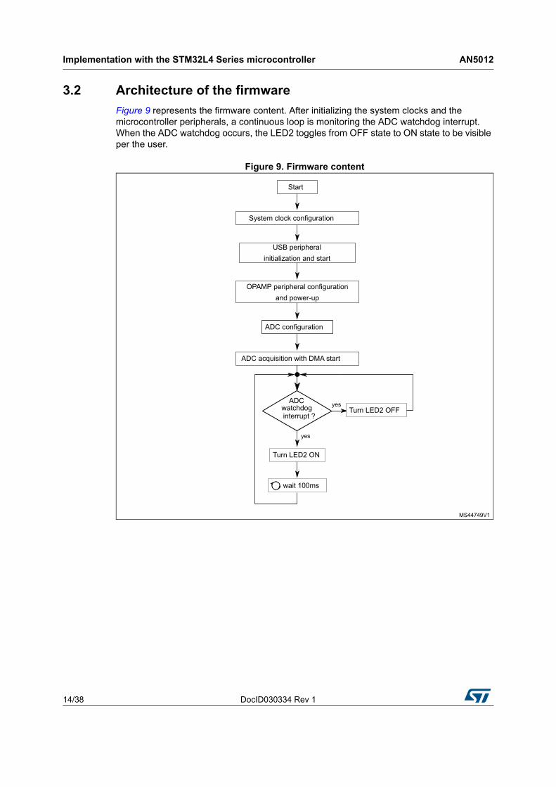
3.2 Architecture of the firmware
Figure 9 represents the firmware content. After initializing the system clocks and the microcontroller peripherals, a continuous loop is monitoring the ADC watchdog interrupt. When the ADC watchdog occurs, the LED2 toggles from OFF state to ON state to be visible per the user.
Figure 9. Firmware content

DocID030334 Rev 1 15/38
AN5012 Implementation with the STM32L4 Series microcontroller
37
There is a second firmware mechanism to exchange data between the ADC and the USB device using the DMA, as shown in Figure 10.
Figure 10. DMA data exchange between ADC and US peripherals
Imp
leme
nta
tion
with
the
ST
M3
2L4
Se
ries m
icroco
ntro
llerA
N5
012
16/3
8D
ocID030
334 Re
v 1
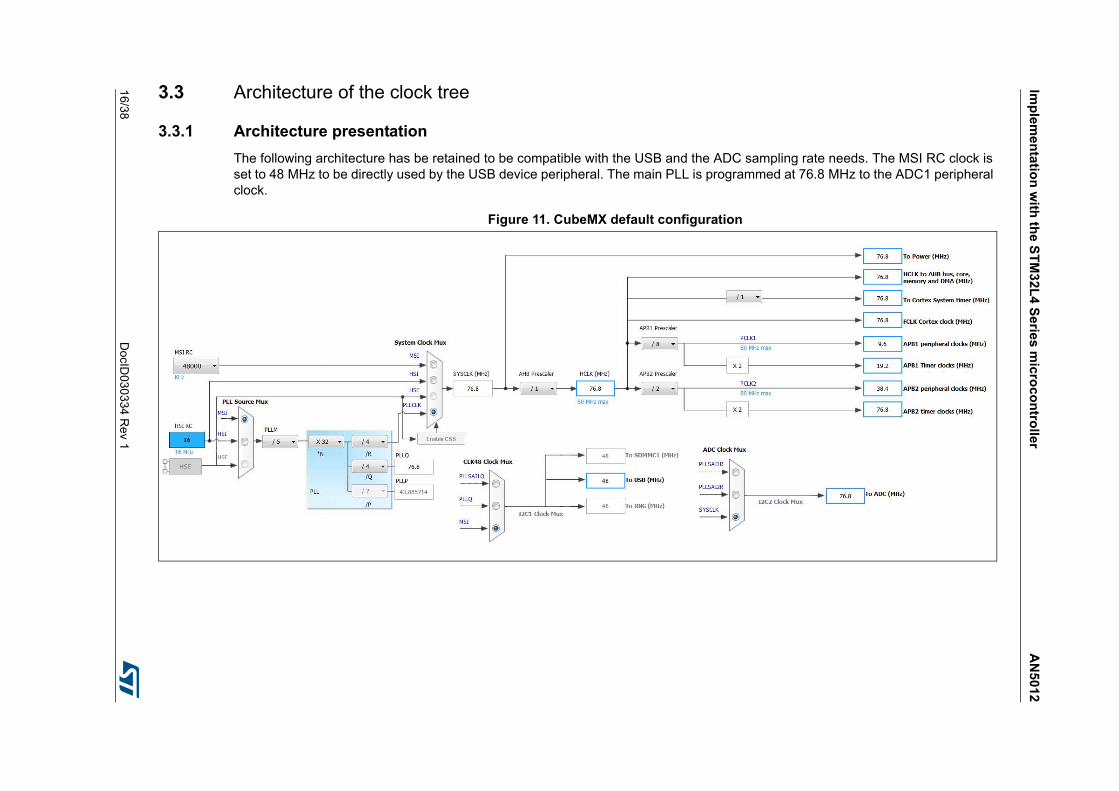
3.3 Architecture of the clock tree
3.3.1 Architecture presentation
The following architecture has be retained to be compatible with the USB and the ADC sampling rate needs. The MSI RC clock is set to 48 MHz to be directly used by the USB device peripheral. The main PLL is programmed at 76.8 MHz to the ADC1 peripheral clock.
Figure 11. CubeMX default configuration
DocID030334 Rev 1 17/38
AN5012 Implementation with the STM32L4 Series microcontroller
37
3.3.2 Clocks constraints and relationship
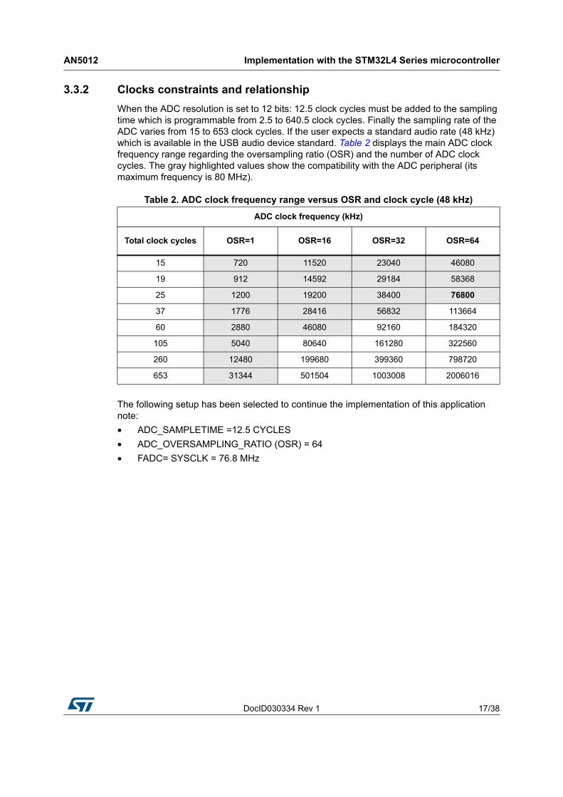
When the ADC resolution is set to 12 bits: 12.5 clock cycles must be added to the sampling time which is programmable from 2.5 to 640.5 clock cycles. Finally the sampling rate of the ADC varies from 15 to 653 clock cycles. If the user expects a standard audio rate (48 kHz) which is available in the USB audio device standard. Table 2 displays the main ADC clock frequency range regarding the oversampling ratio (OSR) and the number of ADC clock cycles. The gray highlighted values show the compatibility with the ADC peripheral (its maximum frequency is 80 MHz).
The following setup has been selected to continue the implementation of this application note:
• ADC_SAMPLETIME =12.5 CYCLES
• ADC_OVERSAMPLING_RATIO (OSR) = 64
• FADC= SYSCLK = 76.8 MHz
Table 2. ADC clock frequency range versus OSR and clock cycle (48 kHz)
ADC clock frequency (kHz)
Total clock cycles OSR=1 OSR=16 OSR=32 OSR=64
15 720 11520 23040 46080
19 912 14592 29184 58368
25 1200 19200 38400 76800
37 1776 28416 56832 113664
60 2880 46080 92160 184320
105 5040 80640 161280 322560
260 12480 199680 399360 798720
653 31344 501504 1003008 2006016
Implementation with the STM32L4 Series microcontroller AN5012
18/38 DocID030334 Rev 1
3.3.3 USB peripheral clocking
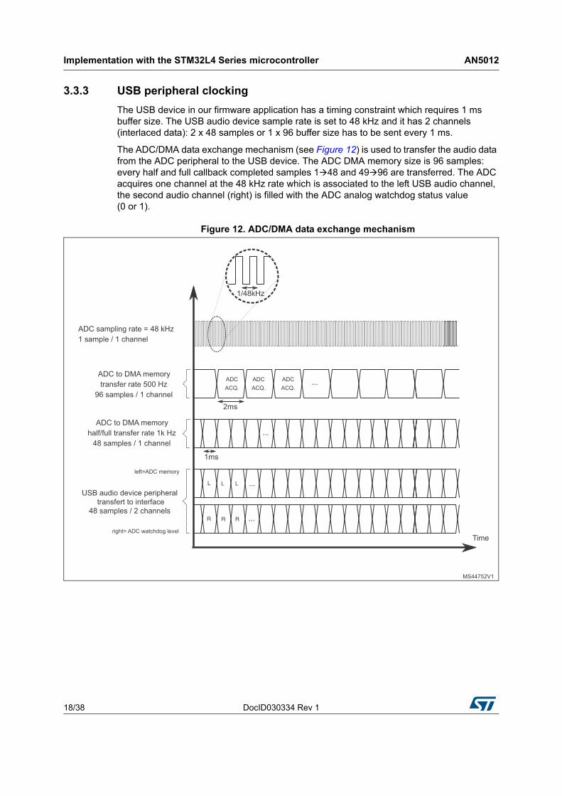
The USB device in our firmware application has a timing constraint which requires 1 ms buffer size. The USB audio device sample rate is set to 48 kHz and it has 2 channels (interlaced data): 2 x 48 samples or 1 x 96 buffer size has to be sent every 1 ms.
The ADC/DMA data exchange mechanism (see Figure 12) is used to transfer the audio data from the ADC peripheral to the USB device. The ADC DMA memory size is 96 samples: every half and full callback completed samples 148 and 4996 are transferred. The ADC acquires one channel at the 48 kHz rate which is associated to the left USB audio channel, the second audio channel (right) is filled with the ADC analog watchdog status value (0 or 1).
Figure 12. ADC/DMA data exchange mechanism
DocID030334 Rev 1 19/38
AN5012 Implementation with the STM32L4 Series microcontroller
37
3.4 Data format (numeric domain)
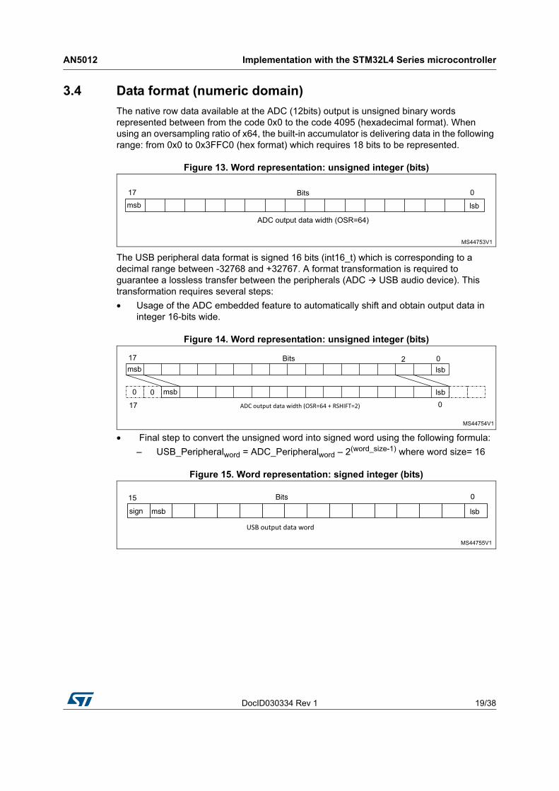
The native row data available at the ADC (12bits) output is unsigned binary words represented between from the code 0x0 to the code 4095 (hexadecimal format). When using an oversampling ratio of x64, the built-in accumulator is delivering data in the following range: from 0x0 to 0x3FFC0 (hex format) which requires 18 bits to be represented.
Figure 13. Word representation: unsigned integer (bits)
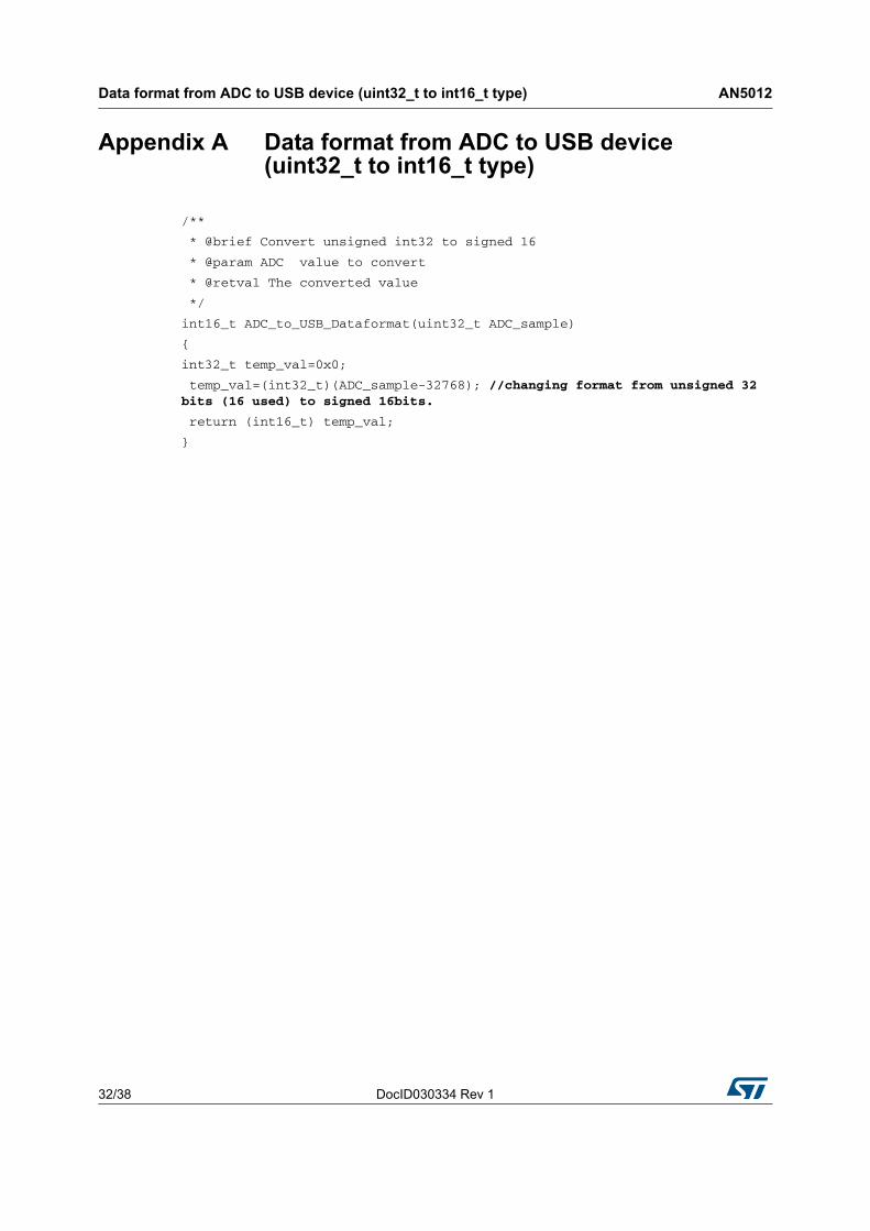
The USB peripheral data format is signed 16 bits (int16_t) which is corresponding to a decimal range between -32768 and +32767. A format transformation is required to guarantee a lossless transfer between the peripherals (ADC USB audio device). This transformation requires several steps:
• Usage of the ADC embedded feature to automatically shift and obtain output data in integer 16-bits wide.
Figure 14. Word representation: unsigned integer (bits)
• Final step to convert the unsigned word into signed word using the following formula:
– USB_Peripheralword = ADC_Peripheralword – 2(word_size-1) where word size= 16
Figure 15. Word representation: signed integer (bits)
Implementation with the STM32L4 Series microcontroller AN5012
20/38 DocID030334 Rev 1
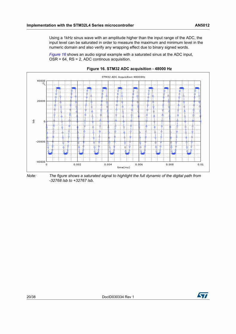
Using a 1kHz sinus wave with an amplitude higher than the input range of the ADC, the input level can be saturated in order to measure the maximum and minimum level in the numeric domain and also verify any wrapping effect due to binary signed words.
Figure 16 shows an audio signal example with a saturated sinus at the ADC input, OSR = 64, RS = 2, ADC continous acquisition.
Figure 16. STM32 ADC acquisition - 48000 Hz
Note: The figure shows a saturated signal to highlight the full dynamic of the digital path from -32768 lsb to +32767 lsb.

DocID030334 Rev 1 21/38
AN5012 Application
37
4 Application
A basic application covered with this application note is the voice activity detection with a programmable threshold level. Once the detection occurs, the device can start the audio recording which will be stored for an embedded signal processing or can immediately transfer the audio data to another peripheral or system.
4.1 Simple voice detection using ADC watchdog feature
The STM32 ADC embeds an analog watchdog which is a very useful feature to detect a certain threshold or window level. The STM32 ADC watchdog has 2 programmable thresholds (low and high) which are defining a normal operation window. Outside of this window, the watchdog interrupt callback appears.
Figure 17 shows both the audio signal and the analog watchdog interrupt signal embedded in the USB audio frame (left channel is the audio from ADC and the right channel is the watchdog interrupt ‘0’ for status <<0>> or ‘16384’ for status <<1>>).
Figure 17. Audio and ADC analog watchdog (threshold +/- 128)
The programmable threshold must be chosen regarding the product application and its environment. If it is very noisy, a large watchdog window is preferable while a quiet ambient noise allows to set a reduced window size.
Application AN5012
22/38 DocID030334 Rev 1
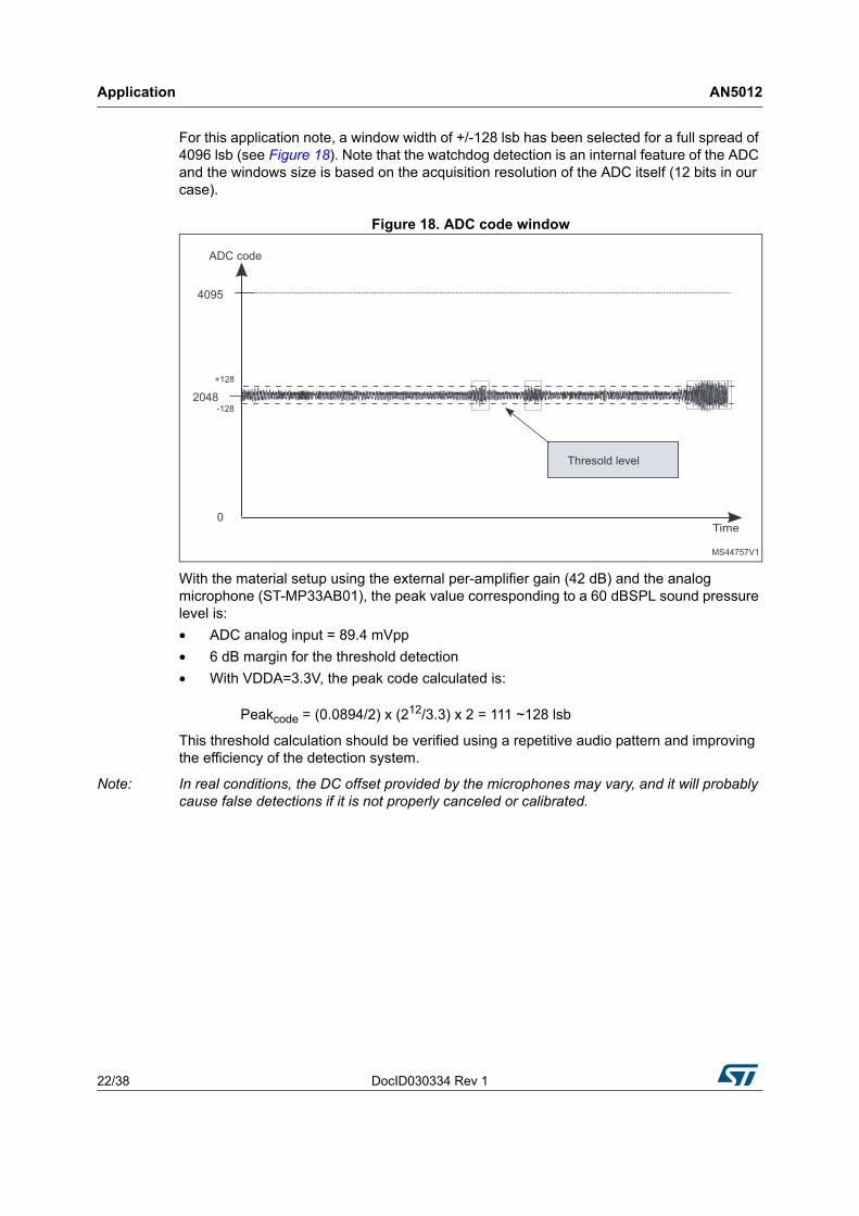
For this application note, a window width of +/-128 lsb has been selected for a full spread of 4096 lsb (see Figure 18). Note that the watchdog detection is an internal feature of the ADC and the windows size is based on the acquisition resolution of the ADC itself (12 bits in our case).
Figure 18. ADC code window
With the material setup using the external per-amplifier gain (42 dB) and the analog microphone (ST-MP33AB01), the peak value corresponding to a 60 dBSPL sound pressure level is:
• ADC analog input = 89.4 mVpp
• 6 dB margin for the threshold detection
• With VDDA=3.3V, the peak code calculated is:
Peakcode = (0.0894/2) x (212/3.3) x 2 = 111 ~128 lsb
This threshold calculation should be verified using a repetitive audio pattern and improving the efficiency of the detection system.
Note: In real conditions, the DC offset provided by the microphones may vary, and it will probably cause false detections if it is not properly canceled or calibrated.
DocID030334 Rev 1 23/38
AN5012 Audio measurements definition
37
5 Audio measurements definition
5.1 Offset measurement
The offset measurement is the mean value of the output signal (numeric domain). Normally, the system should deliver an output signal around the mid-scale of the system. In this application, the mid-scale values for the ADC output is 0x7FFF (unsigned 16 bits) and for the USB audio device it is 0x0000 (signed 16 bits). When a signal is acquired, the user can compare the signal output average with the mid-scale of the system (ADC or USB)
5.2 Frequency response measurement
This measurement is used to define the frequency range of the audio system. Most of the time, the amplitude of the output level at 1 kHz is used as a reference which is compared to the measured amplitude. Concretely, the amplitude of the output signal is measured with a list a frequencies (20 Hz20 kHz) and the attenuation in dB is calculated versus the reference (1 kHz amplitude). An audio system with a flat frequency (+/- 1dB) does not alter the audio signal and its content which will guarantee a good audio rendering.
5.3 Dynamic-range measurement
The dynamic-range measurement is defined by the ratio in dB between the maximum output level and its noise level (minimum output signal).
5.4 Total Harmonic Distortion
The THD represents the linearity performances of the application. During this test, a single tone is applied to the input of audio system. Mathematically, the harmonics are extracted of the input fundamental and the ratio is calculated in dB or percentage between the main tone and its distortion (harmonics).
Signal acquisition measurements AN5012
24/38 DocID030334 Rev 1
6 Signal acquisition measurements
The measurement conditions are:
– Signal generator (Audio Precision APx 526)
– VDDA = 3.3 V
– OPAMP GAIN = 24 dB
– ADC OSR = 64
The following figures show the audio measurements done with the STM32L4 Series device.
AN
501
2S
ign
al a
cq
uis
ition
me
asu
reme
nts
DocID
030334 R
ev 1
25/38
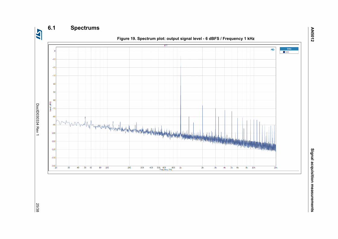
6.1 Spectrums
Figure 19. Spectrum plot: output signal level - 6 dBFS / Frequency 1 kHz
Sig
na
l ac
qu
isition
me
asu
reme
nts
AN
501
2
26/3
8D
ocID030
334 Re
v 1
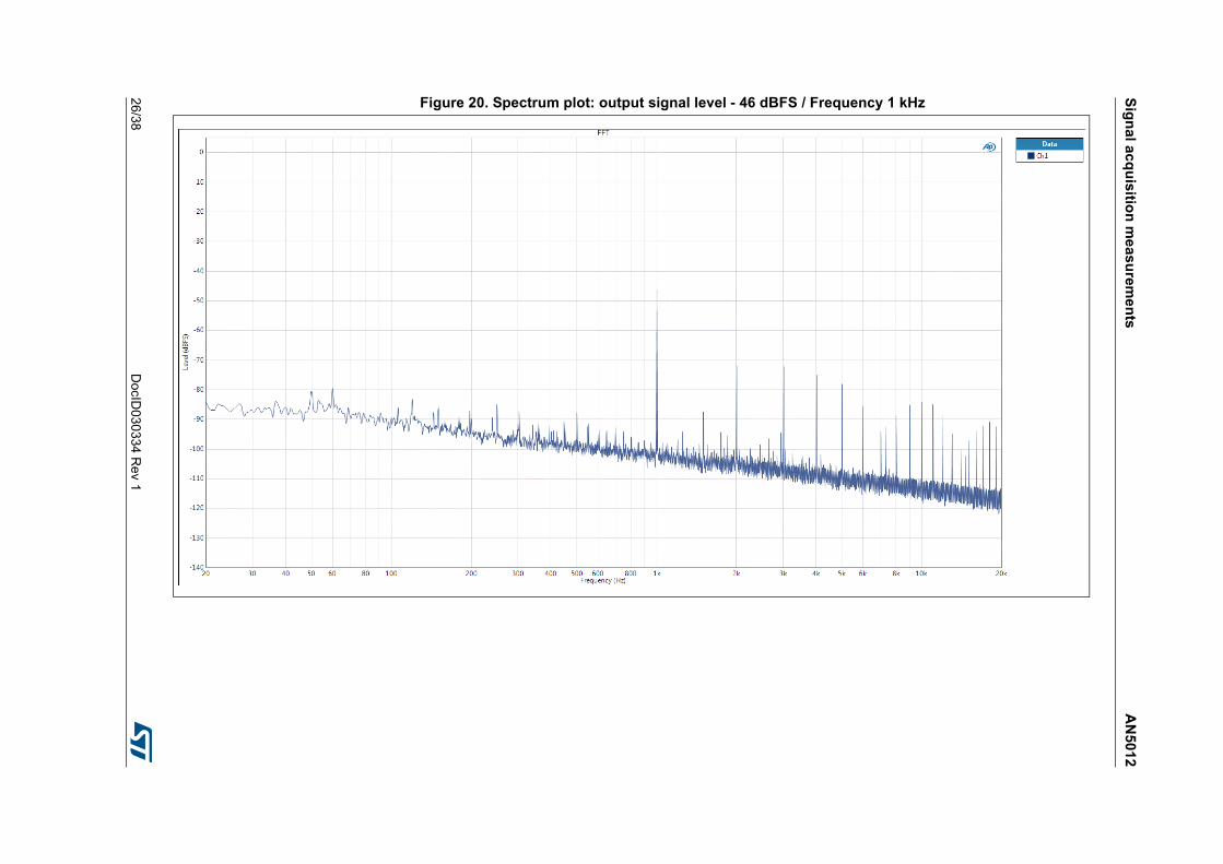
Figure 20. Spectrum plot: output signal level - 46 dBFS / Frequency 1 kHz
DocID030334 Rev 1 27/38
AN5012 Signal acquisition measurements
37
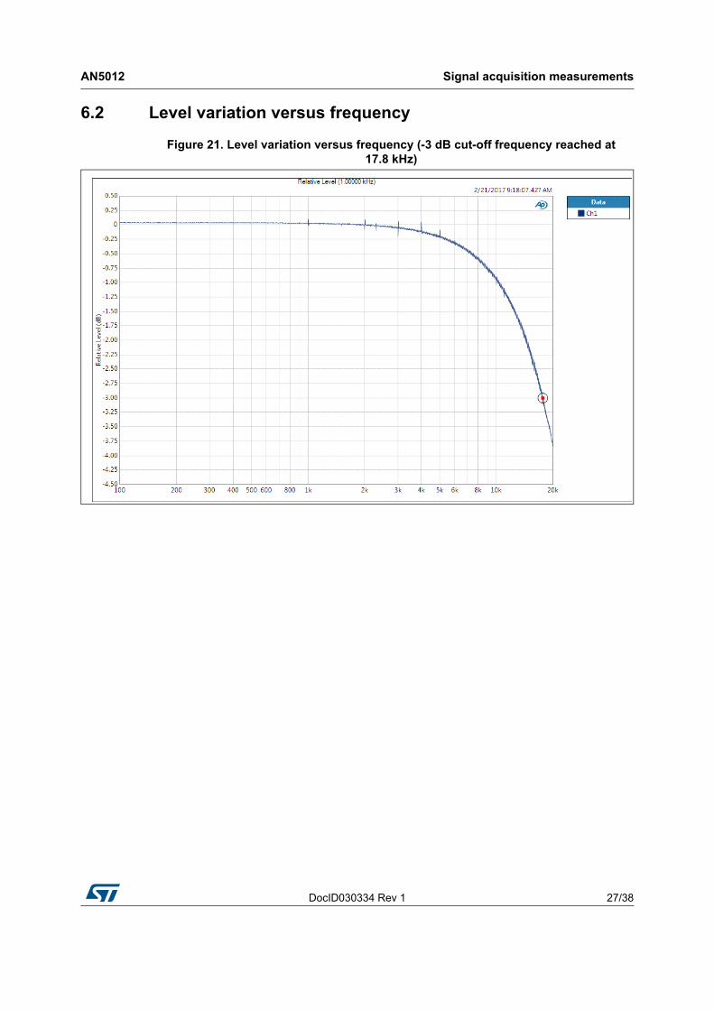
6.2 Level variation versus frequency
Figure 21. Level variation versus frequency (-3 dB cut-off frequency reached at 17.8 kHz)
Signal acquisition measurements AN5012
28/38 DocID030334 Rev 1
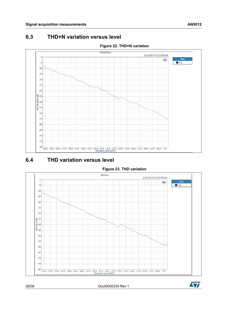
6.3 THD+N variation versus level
Figure 22. THD+N variation
6.4 THD variation versus level
Figure 23. THD variation
DocID030334 Rev 1 29/38
AN5012 Signal acquisition measurements
37
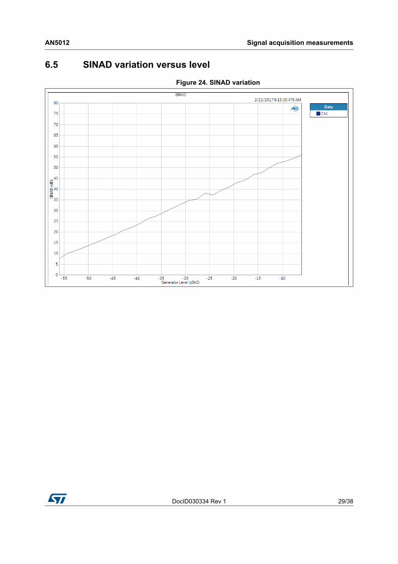
6.5 SINAD variation versus level
Figure 24. SINAD variation
Signal acquisition measurements AN5012
30/38 DocID030334 Rev 1
6.6 Measurement summary
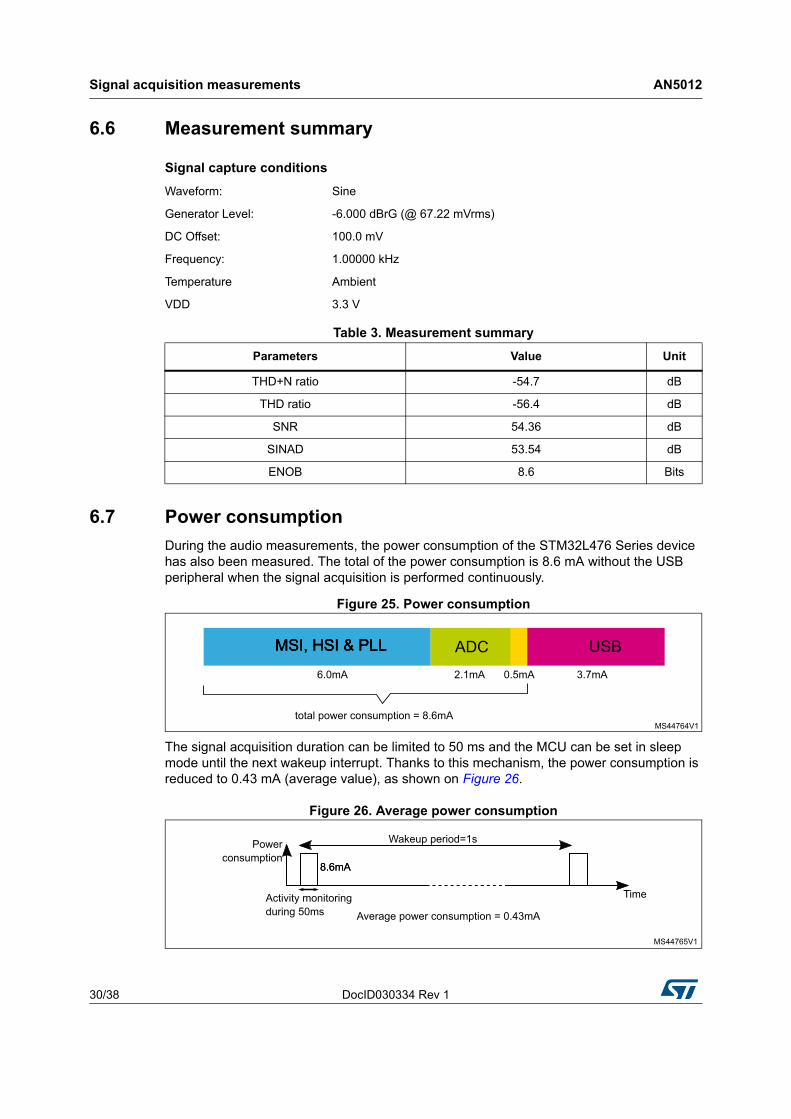
6.7 Power consumption
During the audio measurements, the power consumption of the STM32L476 Series device has also been measured. The total of the power consumption is 8.6 mA without the USB peripheral when the signal acquisition is performed continuously.
Figure 25. Power consumption
The signal acquisition duration can be limited to 50 ms and the MCU can be set in sleep mode until the next wakeup interrupt. Thanks to this mechanism, the power consumption is reduced to 0.43 mA (average value), as shown on Figure 26.
Figure 26. Average power consumption
Signal capture conditions
Waveform: Sine
Generator Level: -6.000 dBrG (@ 67.22 mVrms)
DC Offset: 100.0 mV
Frequency: 1.00000 kHz
Temperature Ambient
VDD 3.3 V
Table 3. Measurement summary
Parameters Value Unit
THD+N ratio -54.7 dB
THD ratio -56.4 dB
SNR 54.36 dB
SINAD 53.54 dB
ENOB 8.6 Bits

DocID030334 Rev 1 31/38
AN5012 Measurement conclusions
37
7 Measurement conclusions
A signal acquisition application from an analog microphone can be done in a very simple way using the STM32L476 Series microcontroller with its embedded OPAMP and ADC peripherals and the dedicated ADC features (oversampling ratio, watchdog).
The global performance is interesting for a simple consumer application to detect, store and post-process an audio signal from an analog microphone.
The OPAMP is increasing the noise level at the input of the ADC but is also introducing some non-linearity.
Data format from ADC to USB device (uint32_t to int16_t type) AN5012
32/38 DocID030334 Rev 1
Appendix A Data format from ADC to USB device (uint32_t to int16_t type)
/**
* @brief Convert unsigned int32 to signed 16
* @param ADC value to convert
* @retval The converted value
*/
int16_t ADC_to_USB_Dataformat(uint32_t ADC_sample)
{
int32_t temp_val=0x0;
temp_val=(int32_t)(ADC_sample-32768); //changing format from unsigned 32 bits (16 used) to signed 16bits.
return (int16_t) temp_val;
}
DocID030334 Rev 1 33/38
AN5012 Octave script
37
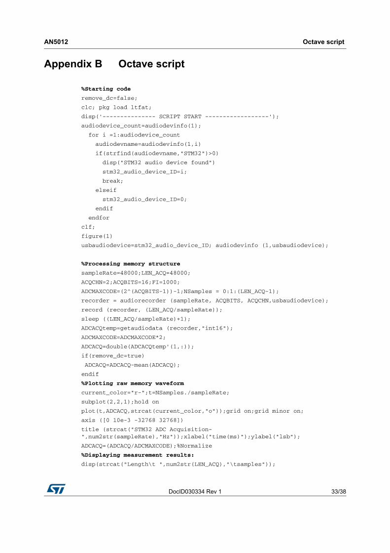
Appendix B Octave script
%Starting code
remove_dc=false;
clc; pkg load ltfat;
disp('--------------- SCRIPT START ------------------');
audiodevice_count=audiodevinfo(1);
for i =1:audiodevice_count
audiodevname=audiodevinfo(1,i)
if(strfind(audiodevname,"STM32")>0)
disp("STM32 audio device found")
stm32_audio_device_ID=i;
break;
elseif
stm32_audio_device_ID=0;
endif
endfor
clf;
figure(1)
usbaudiodevice=stm32_audio_device_ID; audiodevinfo (1,usbaudiodevice);
%Processing memory structure
sampleRate=48000;LEN_ACQ=48000;
ACQCHN=2;ACQBITS=16;FI=1000;
ADCMAXCODE=(2^(ACQBITS-1))-1;NSamples = 0:1:(LEN_ACQ-1);
recorder = audiorecorder (sampleRate, ACQBITS, ACQCHN,usbaudiodevice);
record (recorder, (LEN_ACQ/sampleRate));
sleep ((LEN_ACQ/sampleRate)+1);
ADCACQtemp=getaudiodata (recorder,"int16");
ADCMAXCODE=ADCMAXCODE*2;
ADCACQ=double(ADCACQtemp'(1,:));
if(remove_dc=true)
ADCACQ=ADCACQ-mean(ADCACQ);
endif
%Plotting raw memory waveform
current_color="r-";t=NSamples./sampleRate;
subplot(2,2,1);hold on
plot(t,ADCACQ,strcat(current_color,"o"));grid on;grid minor on;
axis ([0 10e-3 -32768 32768])
title (strcat("STM32 ADC Acquisition-",num2str(sampleRate),"Hz"));xlabel("time(ms)");ylabel("lsb");
ADCACQ=(ADCACQ/ADCMAXCODE);%Normalize
%Displaying measurement results:
disp(strcat("Length\t ",num2str(LEN_ACQ),"\tsamples"));
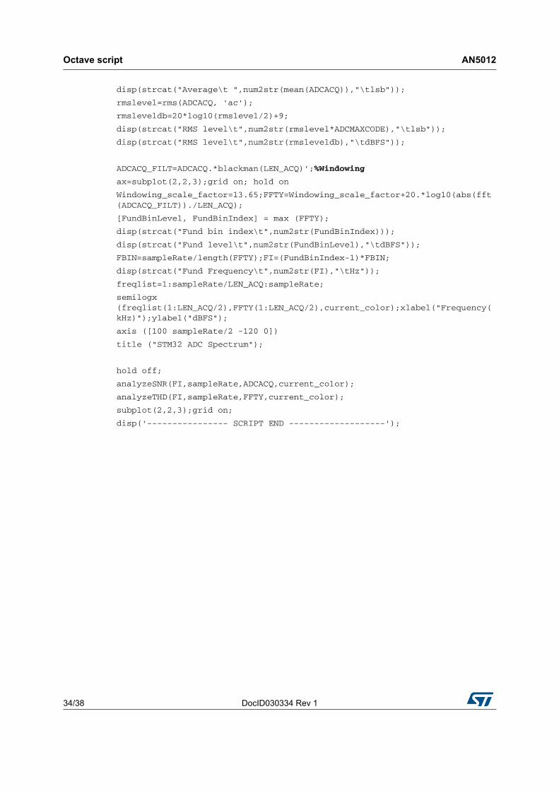
Octave script AN5012
34/38 DocID030334 Rev 1
disp(strcat("Average\t ",num2str(mean(ADCACQ)),"\tlsb"));
rmslevel=rms(ADCACQ, 'ac');
rmsleveldb=20*log10(rmslevel/2)+9;
disp(strcat("RMS level\t",num2str(rmslevel*ADCMAXCODE),"\tlsb"));
disp(strcat("RMS level\t",num2str(rmsleveldb),"\tdBFS"));
ADCACQ_FILT=ADCACQ.*blackman(LEN_ACQ)';%Windowing
ax=subplot(2,2,3);grid on; hold on
Windowing_scale_factor=13.65;FFTY=Windowing_scale_factor+20.*log10(abs(fft(ADCACQ_FILT))./LEN_ACQ);
[FundBinLevel, FundBinIndex] = max (FFTY);
disp(strcat("Fund bin index\t",num2str(FundBinIndex)));
disp(strcat("Fund level\t",num2str(FundBinLevel),"\tdBFS"));
FBIN=sampleRate/length(FFTY);FI=(FundBinIndex-1)*FBIN;
disp(strcat("Fund Frequency\t",num2str(FI),"\tHz"));
freqlist=1:sampleRate/LEN_ACQ:sampleRate;
semilogx (freqlist(1:LEN_ACQ/2),FFTY(1:LEN_ACQ/2),current_color);xlabel("Frequency(kHz)");ylabel("dBFS");
axis ([100 sampleRate/2 -120 0])
title ("STM32 ADC Spectrum");
hold off;
analyzeSNR(FI,sampleRate,ADCACQ,current_color);
analyzeTHD(FI,sampleRate,FFTY,current_color);
subplot(2,2,3);grid on;
disp('---------------- SCRIPT END -------------------');
DocID030334 Rev 1 35/38
AN5012 ADC peripheral configuration function
37
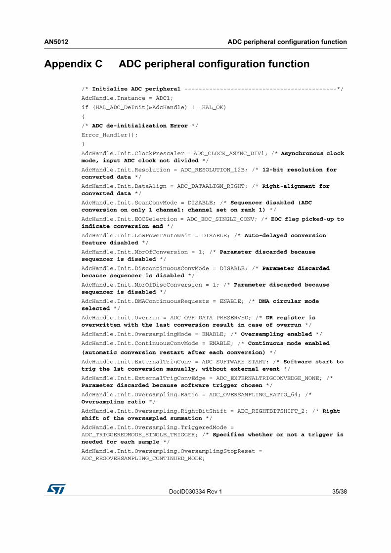
Appendix C ADC peripheral configuration function
/* Initialize ADC peripheral -------------------------------------------*/
AdcHandle.Instance = ADC1;
if (HAL_ADC_DeInit(&AdcHandle) != HAL_OK)
{
/* ADC de-initialization Error */
Error_Handler();
}
AdcHandle.Init.ClockPrescaler = ADC_CLOCK_ASYNC_DIV1; /* Asynchronous clock mode, input ADC clock not divided */
AdcHandle.Init.Resolution = ADC_RESOLUTION_12B; /* 12-bit resolution for converted data */
AdcHandle.Init.DataAlign = ADC_DATAALIGN_RIGHT; /* Right-alignment for converted data */
AdcHandle.Init.ScanConvMode = DISABLE; /* Sequencer disabled (ADC conversion on only 1 channel: channel set on rank 1) */
AdcHandle.Init.EOCSelection = ADC_EOC_SINGLE_CONV; /* EOC flag picked-up to indicate conversion end */
AdcHandle.Init.LowPowerAutoWait = DISABLE; /* Auto-delayed conversion feature disabled */
AdcHandle.Init.NbrOfConversion = 1; /* Parameter discarded because sequencer is disabled */
AdcHandle.Init.DiscontinuousConvMode = DISABLE; /* Parameter discarded because sequencer is disabled */
AdcHandle.Init.NbrOfDiscConversion = 1; /* Parameter discarded because sequencer is disabled */
AdcHandle.Init.DMAContinuousRequests = ENABLE; /* DMA circular mode selected */
AdcHandle.Init.Overrun = ADC_OVR_DATA_PRESERVED; /* DR register is overwritten with the last conversion result in case of overrun */
AdcHandle.Init.OversamplingMode = ENABLE; /* Oversampling enabled */
AdcHandle.Init.ContinuousConvMode = ENABLE; /* Continuous mode enabled
(automatic conversion restart after each conversion) */
AdcHandle.Init.ExternalTrigConv = ADC_SOFTWARE_START; /* Software start to trig the 1st conversion manually, without external event */
AdcHandle.Init.ExternalTrigConvEdge = ADC_EXTERNALTRIGCONVEDGE_NONE; /* Parameter discarded because software trigger chosen */
AdcHandle.Init.Oversampling.Ratio = ADC_OVERSAMPLING_RATIO_64; /* Oversampling ratio */
AdcHandle.Init.Oversampling.RightBitShift = ADC_RIGHTBITSHIFT_2; /* Right shift of the oversampled summation */
AdcHandle.Init.Oversampling.TriggeredMode = ADC_TRIGGEREDMODE_SINGLE_TRIGGER; /* Specifies whether or not a trigger is needed for each sample */
AdcHandle.Init.Oversampling.OversamplingStopReset = ADC_REGOVERSAMPLING_CONTINUED_MODE;

ADC peripheral configuration function AN5012
36/38 DocID030334 Rev 1
/* Specifies whether or not the oversampling buffer is maintained during injection se*/
/* Initialize ADC peripheral according to the passed parameters --------*/
if (HAL_ADC_Init(&AdcHandle) != HAL_OK) {Error_Handler();}
/* Start calibration ----------------------------------------------------*/
if (HAL_ADCEx_Calibration_Start(&AdcHandle, ADC_SINGLE_ENDED) != HAL_OK)
{Error_Handler();}
/* Channel configuration -----------------------------------------------*/
sConfig.Channel = ADCx_CHANNEL; /* Sampled channel number */
sConfig.Rank = ADC_REGULAR_RANK_1; /* Rank of sampled channel number
ADCx_CHANNEL */
sConfig.SamplingTime = ADC_SAMPLETIME_12CYCLES_5; /* Sampling time (number of clock cycles unit) total is 12.5+12.5=25 cycles */
sConfig.SingleDiff = ADC_SINGLE_ENDED; /* Single-ended input channel */
sConfig.OffsetNumber = ADC_OFFSET_NONE; /* No offset subtraction */
sConfig.Offset = 0; /* Parameter discarded because offset correction is
disabled */
if (HAL_ADC_ConfigChannel(&AdcHandle, &sConfig) != HAL_OK)
{Error_Handler();}
/* Set analog watchdog thresholds*/
/* See AN5012 chapter : "Simple voice detection using ADC watchdog feature" */
/* - High threshold: from ADC middle code (2048) + 128 */
/* - Low threshold: from ADC middle code (2048) - 128 */
/* Analog watchdog 1 configuration */
AnalogWDGConfig.WatchdogNumber = ADC_ANALOGWATCHDOG_1;
AnalogWDGConfig.WatchdogMode = ADC_ANALOGWATCHDOG_SINGLE_REG;
AnalogWDGConfig.Channel = ADCx_CHANNEL;
AnalogWDGConfig.ITMode = ENABLE;
AnalogWDGConfig.HighThreshold = 2048+128;
AnalogWDGConfig.LowThreshold = 2048-128;
if (HAL_ADC_AnalogWDGConfig(&AdcHandle, &AnalogWDGConfig) != HAL_OK)
{
/* Channel Configuration Error */
Error_Handler();
}
/* Timer enable ---------------------------------------------------------*/
//if (HAL_TIM_Base_Start_IT(&TimHandle) != HAL_OK)
//{Error_Handler();}
/* Start conversion in DMA mode ----------------------------------------*/
if (HAL_ADC_Start_DMA(&AdcHandle, aResultDMA, ADC_ACQ_LENGHT) != HAL_OK)
{Error_Handler();}
}
DocID030334 Rev 1 37/38
AN5012 Revision history
37
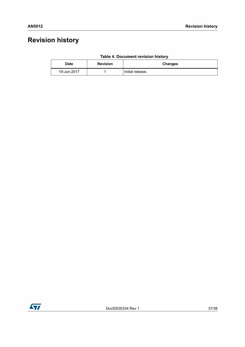
Revision history
Table 4. Document revision history
Date Revision Changes
19-Jun-2017 1 Initial release.
AN5012
38/38 DocID030334 Rev 1
IMPORTANT NOTICE – PLEASE READ CAREFULLY
STMicroelectronics NV and its subsidiaries (“ST”) reserve the right to make changes, corrections, enhancements, modifications, and improvements to ST products and/or to this document at any time without notice. Purchasers should obtain the latest relevant information on ST products before placing orders. ST products are sold pursuant to ST’s terms and conditions of sale in place at the time of order acknowledgement.
Purchasers are solely responsible for the choice, selection, and use of ST products and ST assumes no liability for application assistance or the design of Purchasers’ products.
No license, express or implied, to any intellectual property right is granted by ST herein.
Resale of ST products with provisions different from the information set forth herein shall void any warranty granted by ST for such product.
ST and the ST logo are trademarks of ST. All other product or service names are the property of their respective owners.
Information in this document supersedes and replaces information previously supplied in any prior versions of this document.
© 2017 STMicroelectronics – All rights reserved