analog mos circuits implementing a temporal coding neural...
TRANSCRIPT
PAPER
Analog MOS Circuits Implementing a Temporal Coding Neural Model
Gessyca Maria Tovar, Tetsuya Asai, Daichi Fujita and Yoshihito Amemiya
Graduate School of Information Science and Technology, Hokkaido UniversityKita 14, Nishi 9, Kita-ku, Sapporo 060-0814, Japan
E-mail: [email protected]
Abstract One of the most important processes of the brain is learning and recalling information; the memory func-tion. Because the world in which we live is continuously changing, it is essential for intelligent systems to encode,recognize and generate temporal patterns. Therefore, temporal information processing has great significance in bio-inspired memory systems. A possible model for the storage of temporal sequences was proposed in [1]. On the basis ofthis model, we propose a neural model capable of learning and recalling temporal sequences. The model is designedto be suitable for implementation in analog metal-oxide-semiconductor (MOS) circuits. In this paper, we numericallyconfirmed basic operations of the model. Moreover, we demonstrated fundamental circuit operations and confirmedoperations of the circuit network consisting of 20 neurons using a simulation program with integrated circuit emphasis(SPICE).
Keywords: neural networks, analog MOS circuits, temporal coding, oscillators
1. Introduction
The brain has the ability to process information that changesover time. Therefore, it is necessary that systems, whethernatural or artificial, have the ability to process informationthat depends on the temporal order of events. Studies on neu-roimaging have provided evidence that the prefrontal cortexof the brain is involved in temporal sequencing [2]. Further-more, studies on the olfactory bulb have shown that infor-mation in biological networks takes the form of space-timeneural activity patterns [3], [4].
Patterns whose content depends on time are commonlycalled temporal sequence. The processing of temporal se-quences has been a long-standing problem in artificial neuralnetworks. To process such kind of sequences, a short-termmemory is needed to extract and store the temporally orderedsequences, and another mechanism is needed to retrieve them.Neural networks for processing temporal sequences are usu-ally based on the multilayer perceptron or on the Hopfieldmodels [5]. In [6], a network for processing temporal se-quences has been proposed and applied to robotics. Makinguse of the Hebbian rule, the model is able to learn and recallmultiple trajectories with the help of time-varying informa-tion. In addition, spatio-temporal sequence processing havebeen employed in neuromorphic VLSIs to mimic early visualprocessing [7] and associative memory functions [8].
In this paper, we focus on the implementation of such kindof temporal-coding neural networks in analog metal-oxide-
semiconductor (MOS) devices. In [1], Fukai proposed amodel for the storage of temporal sequences. In the model,the Walsh series expansion [9] was used to represent the inputsignal by linear superposition of rectangular periodic func-tions with different fundamental frequencies generated byan oscillatory subsystem. Often, the development of math-ematical models for simulating large-scale neural networkssuffers from problems of computer load (simulation time).This is avoided by using analog MOS circuits, which per-mit real-time emulation of large-scale networks because, incontrast to discrete step processing (carried out in computersimulations), one can design analog neural circuits in a par-allel manner if a parallel computing structure, based on theconstruction of the brain, is known. Therefore, based onFukai’s model we propose a modified neural model that issuitable for implementation with analog MOS circuits and iscapable of learning and recalling temporal sequences. Themodel consists of neural oscillators coupled to a commonoutput cell through positive or negative synaptic connections.The weights of the synaptic connections are strengthened (orweakened) when the output of the oscillatory cells overlap (ordo not overlap) with the input sequence.
This paper is organized as follows: Section 2 explains thestructure and operations of our temporal coding model in-cluding the numerical simulation results. Section 3 presentsMOS circuit implementation of the model. In section 4 wedemonstrate the operation of the circuit network using a simu-lation program with integrated circuit emphasis (SPICE), andwe conclude our work in section 5.

∑N
i=1
u(t) = wiQ
i(t)
Walsh series
expansion
1Q
2Q
3Q
NQ
I(t)
T
output
cell
temporal input
w1
w2
w3
wN
Fig. 1 Proposed temporal coding model
2. Temporal Coding Model for Analog MOS Circuits
Fukai proposed a model for the storage of temporal sequencesin [1]. The main purpose of this model is the learning andthe recalling of the temporal input stimuli. The model con-sists of an input unit that triggers the oscillatory subsystem.The oscillatory subsystem hasN oscillatory subunits and anarray of modifier cells. Each subunit consists of a pair ofexcitatory and inhibitory neural cells based on the Wilson-Cowan system [10] and generates oscillatory activity withvarious rhythms and phases. These oscillatory cells are con-nected through synaptic connections to an array of modifiercells which transforms the oscillatory activity into rectangu-lar patterns, and controls their rhythms and phases. The out-puts of the modifier cells are connected to an output cell,which is trained independently of the activity of modifiercells, through synaptic connections. The output cell sums upall the outputs of the modifier cells to recall the input signalin accordance with the Walsh function series [9].
Based on the Fukai’s model, we propose a modified modelfor learning and recalling temporal sequences that is suitablefor implementation with analog MOS circuits. The modi-fied model is shown in Fig. 1. One of the characteristics ofFukai’s model is the use of modifier cells. The modifier cellschange the activities of the oscillatory cells into rectangularpatterns,i.e., the cells generate square-wave oscillations. Inaddition, threshold values of the modifier cells are modified toimprove the accuracy of the input-output approximation aftereach learning cycle [1]. In our modified model, we elimi-nated these modifier cells. Instead we used neural oscilla-tors that exhibit periodic square-wave oscillations. Therefore,the modification of thresholds in modifier cells is not carriedout, which results in reducing accuracy of the learning in ourmodel.
0
1Q
T update and reset terms
2
0
1
Q1
singlelearning
cycle0
1
I(t)
time
startingphase
j j+1 j+2
learning cycle
Fig. 2 Definition of single learning cycle
The function of the model is to learn (record) temporalinput sequenceI(t) (∈ 0, 1) of lengthT and to recall it asrecorded sequenceu(t). The model consists ofN neural os-cillators whose outputsQi(t) (∈ 0, 1; i = 1, ..., N ) are time-varying periodic square waves with different fundamental fre-quencies. Each of the oscillators is connected to an output cellthrough synaptic connections whose weights are denoted bywi (i = 1, ..., N ). The output cell calculates the weightedsum of the oscillator outputs as
u(t) =N∑
i=1
wiQi(t) (1)
Through cyclic learning processes,wis in Eq. (1) are updatedat every cycle to achieveu(t) → I(t). Note that this expres-sion,i.e., a weighted sum of square-wave functions with var-ious fundamental frequencies, corresponds to a form of theWalsh series expansion [9], which is a mathematical methodto approximate a certain class of functions, like the Fourierseries expansion.
Now, given a periodic input signal (I(t)) with period Tand the output (u(t)), we define the mean square error (E)between them as
E =1
2T
∫ (j+1)T
jT
[I(t) − u(t)]2 dt (j = 0, 1, 2, · · ·) (2)
wherej represents the learning cycle. To learn the input sig-nal (I(t)) correctly, we need to minimize this error. This isachieved by modifying the weights (wi) between the oscilla-tors and the output cell according to the gradient descent rule:
δwi = −η∂E/∂wi (3)
whereη represents a small positive constant indicating the
0 0.1 0.2 0.2 0.4 0.5 0.6 0.7 0.8 0.9 1
I(t)
time
I(t)
I(t)
u(t)
u(t)
(a) 1st learning
(b) 10th learning
(c) 100th learning
1
0
1
0
1
0u(t)
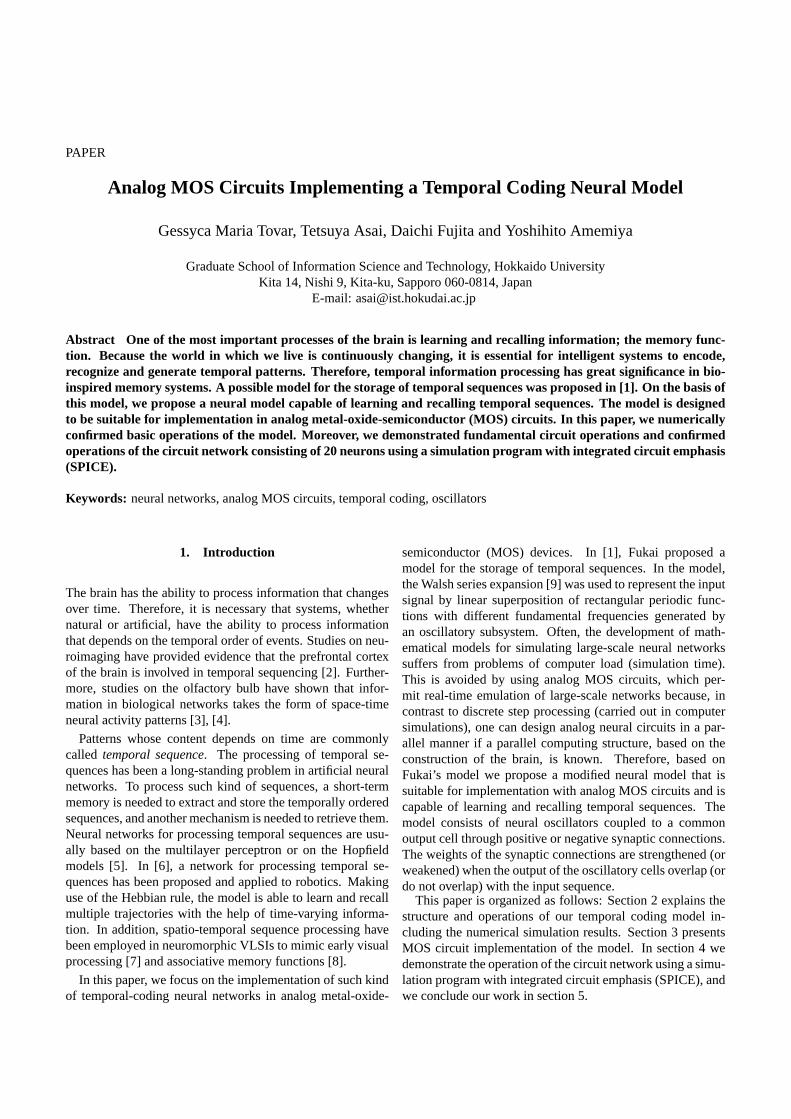
Fig. 3 Input (I(t)) and output sequences (u(t)) of pro-posed network with 200 oscillatory units after first(a) 10th (b) and 100th learning (c)
learning rate. SubstitutingE in Eq. (2) into Eq. (3), we obtain
δwi =η
T
∫ (j+1)T
jT
[I(t) − u(t)]Qi(t) dt (4)
The weights are updated at the end of each learning cycle(t = (j + 1)T ) as
wnewi = wold
i + δwi (5)
The procedures above,i.e., numerical calculations of Eqs. (1),(4) and (5), are repeated (j = 0, 1, · · ·) until the error betweenthe input and the output becomes small enough.
Because our model is meant for hardware implementation,it is necessary to take physical time for updating the weights(Eq. (5)) and resetting the integrated value in Eq. (4) beforestarting another learning cycle, even though the updating andresetting terms are assumed to be zero in Eqs. (4) and (5).In practical hardware, a single learning cycle consists of theinput sequence’s length (T ), and the updating and resettingterms, as shown in Fig. 2. Note that each oscillator’s start-ing phase must be the same at the beginning of each learningcycle. For example, oscillatorsQ1 andQ2 in Fig. 2 have thesame starting phase at the beginning of each learning cycle. Ifthe starting phases ofQis at thej-th learning cycle are differ-ent from that ofQis at the(j + 1)-th cycle, the update valueat the end of thej-th cycle (δwi) has no meaning. Becausetheδwi is calculated by phase activities ofQis in thej-th cy-cle, and is effective only for decreasing errors withQis in the(j+1)-th cycle that has the same starting phases as in thej-thcycle.
0
0.2
0.4
0.6
0.8
1
1.2
1.4
1.6
1 10 100
N=200
N=100 N=30
N=1
me
an
sq
ua
re e
rro
r E
learning cycle j
Fig. 4 Time evolution of mean square errors
Numerical simulations were conducted to confirm the op-eration of the model. In the simulation, output of the oscilla-tory unitsQi(t) was defined by
Qi(t) = H[sin(2πfit)] (6)
wherefi represents a random frequency distributed between1 and 10 using white noise sources, andH(x) is the step func-tion defined as:
H(x) =
1 (x > 0)
0 (x < 0)(7)
The results are shown in Fig. 3 (N = 200, T = 1 andη = 0.01). After the first learning (Fig. 3(a)), the input (I(t))and the output sequences (u(t)) were completely different;however,u(t) approachedI(t) after repeated learning cycles(Figs. 3(b) for 10th and (c) for 100th learning).
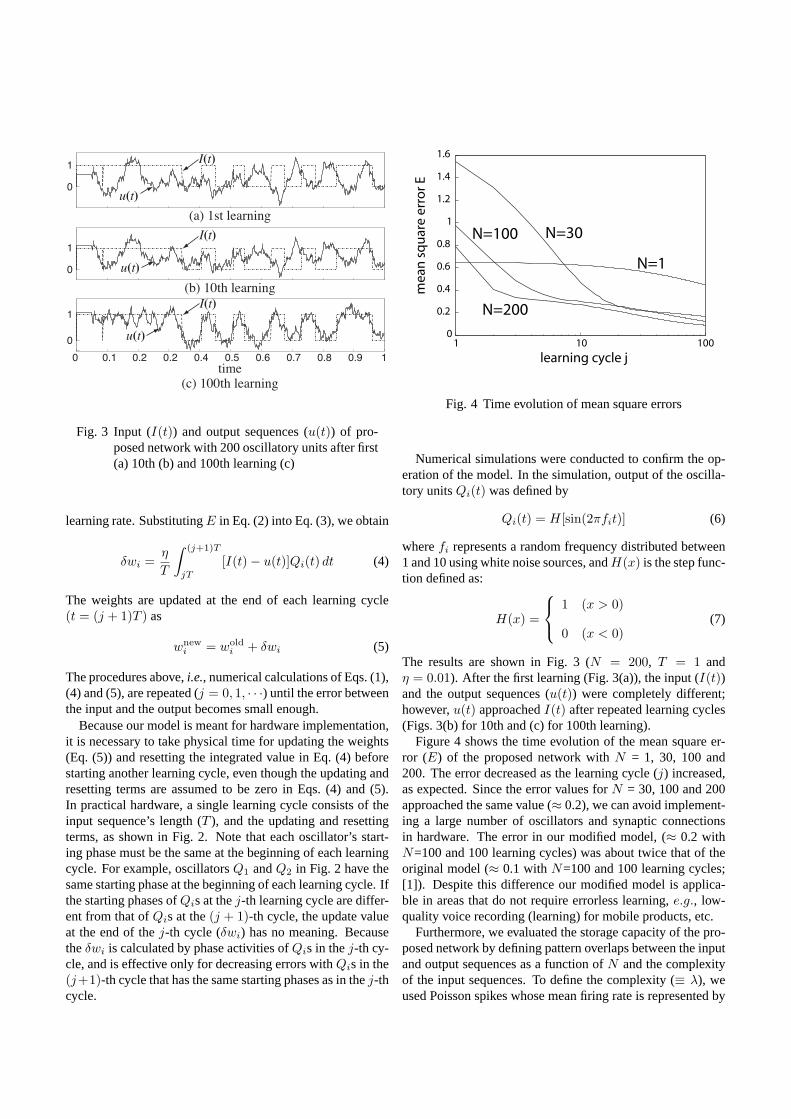
Figure 4 shows the time evolution of the mean square er-ror (E) of the proposed network withN = 1, 30, 100 and200. The error decreased as the learning cycle (j) increased,as expected. Since the error values forN = 30, 100 and 200approached the same value (≈ 0.2), we can avoid implement-ing a large number of oscillators and synaptic connectionsin hardware. The error in our modified model, (≈ 0.2 withN=100 and 100 learning cycles) was about twice that of theoriginal model (≈ 0.1 with N=100 and 100 learning cycles;[1]). Despite this difference our modified model is applica-ble in areas that do not require errorless learning,e.g., low-quality voice recording (learning) for mobile products, etc.
Furthermore, we evaluated the storage capacity of the pro-posed network by defining pattern overlaps between the inputand output sequences as a function ofN and the complexityof the input sequences. To define the complexity (≡ λ), weused Poisson spikes whose mean firing rate is represented by
0
1
λ/T=4
I(t)
T0
Poisson
spikes
time
t1
t2
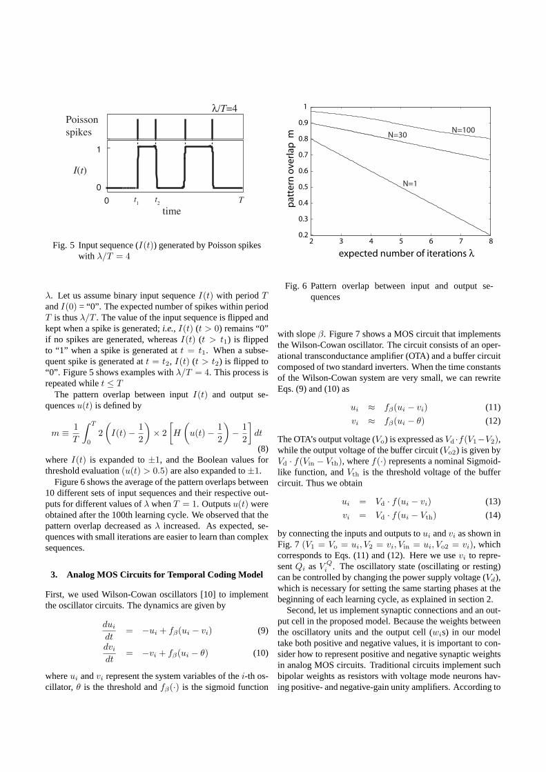
Fig. 5 Input sequence (I(t)) generated by Poisson spikeswith λ/T = 4
λ. Let us assume binary input sequenceI(t) with periodTandI(0) = “0”. The expected number of spikes within periodT is thusλ/T . The value of the input sequence is flipped andkept when a spike is generated;i.e., I(t) (t > 0) remains “0”if no spikes are generated, whereasI(t) (t > t1) is flippedto “1” when a spike is generated att = t1. When a subse-quent spike is generated att = t2, I(t) (t > t2) is flipped to“0”. Figure 5 shows examples withλ/T = 4. This process isrepeated whilet ≤ T
The pattern overlap between inputI(t) and output se-quencesu(t) is defined by
m ≡ 1T
∫ T
0
2(
I(t) − 12
)× 2
[H
(u(t) − 1
2
)− 1
2
]dt
(8)whereI(t) is expanded to±1, and the Boolean values forthreshold evaluation(u(t) > 0.5) are also expanded to±1.
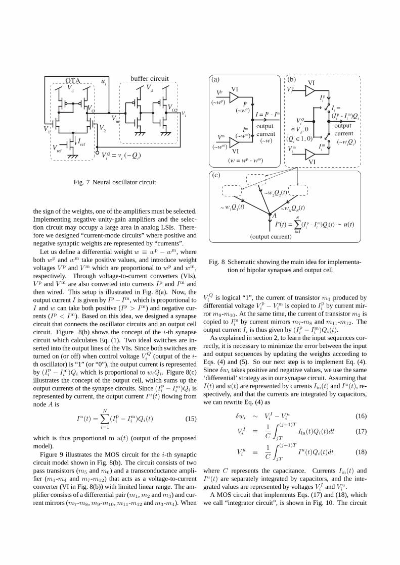
Figure 6 shows the average of the pattern overlaps between10 different sets of input sequences and their respective out-puts for different values ofλ whenT = 1. Outputsu(t) wereobtained after the 100th learning cycle. We observed that thepattern overlap decreased asλ increased. As expected, se-quences with small iterations are easier to learn than complexsequences.
3. Analog MOS Circuits for Temporal Coding Model
First, we used Wilson-Cowan oscillators [10] to implementthe oscillator circuits. The dynamics are given by
dui
dt= −ui + fβ(ui − vi) (9)
dvi
dt= −vi + fβ(ui − θ) (10)
whereui andvi represent the system variables of thei-th os-cillator, θ is the threshold andfβ(·) is the sigmoid function
0.2
0.3
0.4
0.5
0.6
0.7
0.8
0.9
1
2 3 4 5 6 7 8
N=100N=30
N=1
expected number of iterations λ
pa
tte
rn o
ve
rla
p m
Fig. 6 Pattern overlap between input and output se-quences
with slopeβ. Figure 7 shows a MOS circuit that implementsthe Wilson-Cowan oscillator. The circuit consists of an oper-ational transconductance amplifier (OTA) and a buffer circuitcomposed of two standard inverters. When the time constantsof the Wilson-Cowan system are very small, we can rewriteEqs. (9) and (10) as
ui ≈ fβ(ui − vi) (11)
vi ≈ fβ(ui − θ) (12)
The OTA’s output voltage (Vo) is expressed asVd ·f(V1−V2),while the output voltage of the buffer circuit (Vo2) is given byVd · f(Vin − Vth), wheref(·) represents a nominal Sigmoid-like function, andVth is the threshold voltage of the buffercircuit. Thus we obtain
ui = Vd · f(ui − vi) (13)
vi = Vd · f(ui − Vth) (14)
by connecting the inputs and outputs toui andvi as shown inFig. 7 (V1 = Vo = ui, V2 = vi, Vin = ui, Vo2 = vi), whichcorresponds to Eqs. (11) and (12). Here we usevi to repre-sentQi asV Q
i . The oscillatory state (oscillating or resting)can be controlled by changing the power supply voltage (Vd),which is necessary for setting the same starting phases at thebeginning of each learning cycle, as explained in section 2.
Second, let us implement synaptic connections and an out-put cell in the proposed model. Because the weights betweenthe oscillatory units and the output cell (wis) in our modeltake both positive and negative values, it is important to con-sider how to represent positive and negative synaptic weightsin analog MOS circuits. Traditional circuits implement suchbipolar weights as resistors with voltage mode neurons hav-ing positive- and negative-gain unity amplifiers. According to
Vref
Vd
Vi
Q = vi ( Q
i)
Vd
ui
V1
V2
VO2V
O
Vin
OTA buffer circuit
vi
~
Iref
Fig. 7 Neural oscillator circuit
the sign of the weights, one of the amplifiers must be selected.Implementing negative unity-gain amplifiers and the selec-tion circuit may occupy a large area in analog LSIs. There-fore we designed “current-mode circuits” where positive andnegative synaptic weights are represented by “currents”.
Let us define a differential weightw ≡ wp − wm, whereboth wp andwm take positive values, and introduce weightvoltagesV p andV m which are proportional towp andwm,respectively. Through voltage-to-current converters (VIs),V p andV m are also converted into currentsIp andIm andthen wired. This setup is illustrated in Fig. 8(a). Now, theoutput currentI is given byIp− Im, which is proportional toI andw can take both positive (Ip > Im) and negative cur-rents (Ip < Im). Based on this idea, we designed a synapsecircuit that connects the oscillator circuits and an output cellcircuit. Figure 8(b) shows the concept of thei-th synapsecircuit which calculates Eq. (1). Two ideal switches are in-serted into the output lines of the VIs. Since both switches areturned on (or off) when control voltageV Q
i (output of thei-th oscillator) is “1” (or “0”), the output current is representedby (Ip
i − Imi )Qi which is proportional towiQi. Figure 8(c)
illustrates the concept of the output cell, which sums up theoutput currents of the synapse circuits. Since(Ip
i − Imi )Qi is
represented by current, the output currentIu(t) flowing fromnodeA is
Iu(t) =N∑
i=1
(Ipi − Im
i )Qi(t) (15)
which is thus proportional tou(t) (output of the proposedmodel).
Figure 9 illustrates the MOS circuit for thei-th synapticcircuit model shown in Fig. 8(b). The circuit consists of twopass transistors (m5 andm6) and a transconductance ampli-fier (m1-m4 and m7-m12) that acts as a voltage-to-currentconverter (VI in Fig. 8(b)) with limited linear range. The am-plifier consists of a differential pair (m1, m2 andm3) and cur-rent mirrors (m7-m8, m9-m10, m11-m12 andm3-m4). When
A
VI
VI
output
current(Q
i ∈1, 0)
∈Vd, 0
VI
VI
output
current
(a) (b)
(c)
( wp)~
Vp
( wm)~
Vm
Vi
p
Ip
Im
( w)~
I = Ip - Im
Vi
m
Ii
p
Ii
m
Ii =
(Ii
p - Ii
m)Qi
( wp)~
( wm)~
(w = wp - wm)
( wiQ
i)~
w1Q
1(t)
w2Q
2(t)
wNQ
N(t)
(output current)
Iu(t) = (Ii
p - Ii
m)Qi(t)∑
N
i=1
u(t)~
~ ~
~
Vi
Q
Fig. 8 Schematic showing the main idea for implementa-tion of bipolar synapses and output cell
V Qi is logical “1”, the current of transistorm1 produced by
differential voltageV pi − V m
i is copied toIpi by current mir-
ror m9-m10. At the same time, the current of transistorm2 iscopied toIm
i by current mirrorsm7-m8 andm11-m12. Theoutput currentIi is thus given by(Ip
i − Imi )Qi(t).
As explained in section 2, to learn the input sequences cor-rectly, it is necessary to minimize the error between the inputand output sequences by updating the weights according toEqs. (4) and (5). So our next step is to implement Eq. (4).Sinceδwi takes positive and negative values, we use the same‘differential’ strategy as in our synapse circuit. Assuming thatI(t) andu(t) are represented by currentsIin(t) andIu(t), re-spectively, and that the currents are integrated by capacitors,we can rewrite Eq. (4) as
δwi ∼ V Ii − V u
i (16)
V Ii ≡ 1
C
∫ (j+1)T
jT
Iin(t)Qi(t)dt (17)
V ui ≡ 1
C
∫ (j+1)T
jT
Iu(t)Qi(t)dt (18)
where C represents the capacitance. CurrentsIin(t) andIu(t) are separately integrated by capacitors, and the inte-grated values are represented by voltagesV I
i andV ui .
A MOS circuit that implements Eqs. (17) and (18), whichwe call “integrator circuit”, is shown in Fig. 10. The circuit
m
m
m m
m
m
m
m m
m
mm
Iref
Vdd
8 7 9
56
2 1
34
11 12
10
Vi
pVi
m
Ii
p
Ii
m
Ii
Vi
Q
Fig. 9 Synapse circuit calculating weighted sum (Ii) ofoutput of oscillator (V Q
i ) and stored weight volt-ages (V p
i andV mi )
m m
m m
m m
m mVr
Iin(t)
C
17 2 8
34
56
Vin
Vdd
Vu
C
Iu(t)Vi
uVi
I
Vi
Q
Fig. 10 Integrator circuit
consists of two current mirrors (m1-m7 and m2-m8), twopass transistors (m3 andm4), two capacitors (C ’s), and twotransistors for reset operations (m5 andm6). WhenV Q
i isa logical “1”, Iin(t) andIu(t) are copied to pass transistorsm3 andm4, respectively, by the current mirrors, and are in-tegrated by the capacitors. As explained in section 2, beforestarting each learning cycle,V I
i andV ui , must be reset to 0
by settingVr to “1”. Remember that voltagesVin andVu inFig. 10 reflect the temporal input (I(t)) and output sequences(u(t)) that will be used to represent the simulation results insection 4.
Next, let us evaluate the difference between the integratedvoltagesV I
i andV ui to calculate Eq. (16). Assume that the
differential voltage is nonlinearly converted into currentIδi
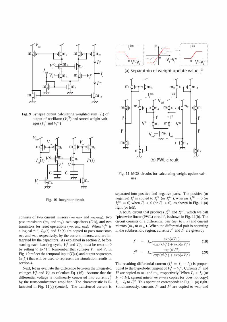
by the transconductance amplifier. The characteristic is il-lustrated in Fig. 11(a) (center). The transferred current is
(a) Separatoin of weight update value Ii
δ
Vref
(b) PWL circuit
Vi
uVi
I
I1 I2I1
I2
Ii
δm Ii
δp
0
Ii
δp
Vi
I-Vi
u0
Ii
δm
Vi
I-Vi
uV
i
I-Vi
u
Ii
δ
0
Iref
m
m
m m
m
m
m
m
m
m
m
m
m m
mm
m
1617
10
12
8
13
9
1415
711
64
1 2
3
5
I1
I2
Vdd
Fig. 11 MOS circuits for calculating weight update val-ues
separated into positive and negative parts. The positive (ornegative)Iδ
i is copied toIδpi (or Iδm
i ), whereasIδpi = 0 (or
Iδmi = 0) whenIδ
i < 0 (or Iδi > 0), as shown in Fig. 11(a)
right (or left).A MOS circuit that producesIδp
i andIδmi , which we call
“piecewise linear (PWL) circuit”, is shown in Fig. 11(b). Thecircuit consists of a differential pair (m1 to m3) and currentmirrors (m4 to m17). When the differential pair is operatingin the subthreshold region, currentsI1 andI2 are given by
I1 = Irefexp(κV I
i )exp(κV I
i ) + exp(κV ui )
(19)
I2 = Irefexp(κV u
i )exp(κV I
i ) + exp(κV ui )
(20)
The resulting differential current (Iδi = I1 − I2) is propor-
tional to the hyperbolic tangent ofV Ii − V u
i . CurrentsI1 andI2 are copied tom7 andm9, respectively. WhenI1 > I2 (orI1 < I2), current mirrorm14-m15 copies (or does not copy)I1 − I2 to Iδp
i . This operation corresponds to Fig. 11(a) right.Simultaneously, currentsI1 and I2 are copied tom10 and

VL
C1 T
0
0
1
1
Vr
0
1
(a) Weights update circuit
m 1
m 2
update and reset terms
learning cycle
C2
Vi
p Vi
m
Ii
δp Ii
δm
VL
update
reset
(b) Timing Chart
Vi
Q
Fig. 12 Weights update circuit and timing chart
m12. WhenI2 > I1 (or I2 < I1), current mirrorm16-m17
copies (or does not copy)I2 − I1 to Iδmi , which corresponds
to characteristics in Fig. 11(a) left.As explained in section 2, at the end of each oscillatory cy-
cle T , the weights have to be updated according to Eq. (5).We have already separatedδwi into positive and negativeparts, as shown in Fig. 11(a), and obtained two positive cur-rentsIδp
i andIδmi . Assuming that the bipolar weights are sep-
arately stored in capacitors and are updated with the amountsof Iδp
i andIδmi , then Eq. (5) can be rewritten as
V pi (t + ∆t) = V p
i (t) +∆t
CIδpi L (21)
V mi (t + ∆t) = V m
i (t) +∆t
CIδmi L (22)
whereC represents the capacitance,∆t the time step of learn-ing, L the normalized binary value (≡ VL/Vdd) for control-ling the weight update,V p
i andV mi the integrated (updated)
weight values. When∆t → 0, we obtain the differentialforms
CdV p
i
dt= Iδp
i L (23)
CdV m
i
dt= Iδm
i L (24)
Figure 12(a) illustrates a MOS circuit that calculates Eqs. (23)and (24). During the update cycle (VL is logical “1”), Iδp
i
andIδmi are separately integrated by capacitorsC1 andC2,
respectively, via pass transistorsm1 andm2. Remember thatthe integrated valuesV p
i andV mi represent the weightwi (∼
V pi − V m
i ), and they are fed back to thei-th synapse circuitshown in Fig. 9.
Figure 12(b) summarizes the circuit’s control voltages persingle learning cycle (timing chart). Before each learning cy-cle is started,Vr is set to logical “1” to reset the weight updatevaluesδwi (V I
i = V ui = 0). At the beginning of each learn-
ing cycle, theVd of the oscillator circuit shown in Fig. 7 is setto Vdd andV Q
i starts to exhibit square-wave oscillations. Atthe end of the oscillatory cycle,Vd is set to 0 (thus the oscil-lation stops) and in turn the weight update begins (VL = “1”).
When the update is finished,Vr is set to “1”. This processis repeated until the difference between the input and outputsequences becomes small enough.
4. Simulation Results
We conducted SPICE simulations for each circuit componentin section 3. In the simulations, we used TSMC0.35-µmCMOS parameters. Figure 13(a) shows the results of a singleoscillator circuit, integrator circuit and PWL circuit. In theoscillator circuit, all the dimensions (W/L) of the transistorswere set to 2µm / 0.24µm, andVref was set to450 mV. Thesupply voltageVd was 2.5 V (or 0). We confirmed that i) thecircuit oscillated when the supply voltage was given, and ii)the starting phases at the beginning of the learning cycles (atVd = 0 → 2.5 V; i.e., t = 0.4 µs and 0.8µs) were the same,as shown in Fig. 13(a).
Simulation results for the integrator circuit are shown inFig. 13(b). All the dimensions of the transistors in the circuitwere set to 0.36µm / 0.24µm. Input currentsIin andIu wereset to 1µA and 2µA, respectively. CapacitanceC was set to1 pF, and the supply voltageVdd was set to 2.5 V. Figure13(b) shows that independently of the control voltageV Q
i ,integrated voltagesV I
i andV ui were reset to 0 when the reset
control voltage (Vr) was set to logical “1” (t = 0 ∼ 0.25 µs).The integration started whenVr was set to “0” andV Q
i was“1”, which resulted in an increase inV I
i andV ui (t = 0.25 ∼
0.5 µs). Then the integration stopped andV Ii andV u
i werepreserved whenV Q
i was “0” (t = 0.5 ∼ 0.75 µs). Again,whenVr was set to “1”, the integrated voltages were reset tozero (t = 0.75 ∼ 1 µs).
Figure 13(c) shows the simulation results for a single PWLcircuit. The transistor dimensions were 7.2µm / 0.24µmfor m7 andm10, 1.6 µm / 0.24µm for m9 andm12, 0.72µm / 0.24 µm for m14 and m17, and 0.36µm / 0.24 µmfor the remaining transistors. The supply voltage (Vdd), V u
i
andVref were set to 2.5 V, 1.25 V and 1 V, respectively. Asshown in Fig. 13(c) we could obtain similar characteristics asFigs. 11(a) left and right;i.e., whenV I
i > V ui , Iδp
i was mono-tonically increased asV I
i increased, whereasIδpi remained
zero whenV Ii < V u
i . On the other hand, whenV Ii > V u
i ,Iδmi was zero whileIδm
i was monotonically decreased asV Ii
increased whenV Ii < V u
i .We confirmed the learning operation of the entire circuit
with N = 20. The fundamental frequencies (fi’s) of the os-cillators were set by
fi ≈ 0.3i + 1.1(MHz) (25)
wherei represents the neuron index, which results in a dis-tribution between 1.4 MHz and 7.1 MHz. The learning cyclewas set to1 µs with T , the updating and the resetting termswere set to 0.7µs, 0.1µs and 0.2µs, respectively. The inputsequences (I(t)) were generated with current pulses of 0.1

0
0.8
2.5
2.5
0 0.25 0.5 0.75 1
0
0
0
2.5
2.5
0 1.6 2
0
time (µs)
0.4 0.8
1.2
0
4.5
0 0.5 1 1.5 2 2.5
ViQ
(V
)V
d (
V)
(a) Oscillator
(b) Integratortime (µs)
Vr (
V)
ViQ
(V
)
Vi
u
Vi
I
ou
tpu
ts (
V)
(c) PWL circuit
Vi
I (V)
ou
tpu
t cu
rre
nts
(µ
A)
Ii
δm Ii
δp
(Vi
u = 1.25 V)
startingphase
Fig. 13 Simulation results of circuit components
µA in amplitude, andλ/T was set to4. CapacitancesC1 andC2 in Fig. 12(a) were set to1 pF, and the supply voltageVdd
was set to2.5 V.
Figure 14(a) shows the timing chart for a single learningcycle. The time evolution of thei-th integrator outputs (V I
i
andV ui ) and those of the weight voltages (V p
i andV mi ) are
shown in Figs. 14(b) and (c), respectively. We could observethatV I
i andV ui took almost the same values;i.e., errors be-
tween the input and output sequences became zero after ap-proximately 20 learning cycles. The weight voltages weresuccessfully updated at the end of each learning cycle; whenV I
i > V ui , the positive weight (V p
i ) was increased, whereas,whenV I
i < V ui the negative weight (V m
i ) was increased, un-til the two attained stable values.
The time courses of temporal input voltageVin (∼ I(t); seeFig. 10) and learned output voltageVu (∼ u(t)) are shownin Figs. 15 and 16. We could observe thatVin andVu weredifferent at the beginning (Fig. 15) but became similar after
0 10 20 30
0 0.2 0.4 0.6 0.8 1
Vr (
V)
time (µs)
0
0
0
2.5
2.5
2.5
1.2
1.8
1.4
1.6
15 2550
1
2
Vd (
V)
VL (
V)
update reset
time (µs)
Vi
u
Vi
I
inte
gra
tor
ou
tpu
ts
(V)
we
igh
t vo
lta
ge
s
(V)
Vi
p
Vi
m
20th learning cycle
learning cycle (1 µs)
T = 0.7 µs (0.1 µs) (0.2 µs)
(a) Timing chart
(b) Time evolution of the i-th integrator output
(c) Evolution of weight voltages
Fig. 14 Simulation results of circuit network withN=20
about 29 learning cycles (Fig. 16).It is important to note that all the MOSFETs in the pro-
posed circuit operate in their sub-threshold region. To ensuresub-threshold operation of the MOSFETs, we set bias voltageVref at the lower values of the MOSFETs threshold voltage,which results in fundamental frequencies of oscillators in theMHz range, (about 1 MHz to 10 MHz for the upper bound fre-quency). Note that, it is possible to learn temporal sequencesin the audio frequency (kHz range) by changing the bias volt-age value (Vref ) of the oscillator circuit from 0.09 V to 0.1V.
Finally, we calculated the pattern overlaps in Eq. (8) be-tween the input and output sequences produced by our cir-cuits for different sets of input sequences (λ). The inputsequences were generated with current pulses of0.5 µA inamplitude. The oscillatory cycle (T ), updating and resettingterms were set to the same values as in the simulations ofFigs. 14 to 16. The calculations were carried out for 1 and30 neuron networks. The fundamental frequencies, set byEq. (25), were distributed between 1.4 MHz and 10.1 MHzfor N=30. Figure 17 shows the averaged pattern overlap be-tween 10 different sets of input sequences and their outputs.For comparison, numerical results of the network model insection 2 with the same number of neurons are also shown
1.6
2
2.4
0 2 4 6 8 10
1.6
2
2.4
time (µs)
input
signal
Vin (
V)
store
d s
ignal
Vu (
V)
1st learning
cycle
10th learning
cycle
Fig. 15 Evolution of temporal input sequenceVin andlearned output sequenceVu (first to 10th learn-ing cycles)
1.9
2
2.1
2.2
30 29
time (µs)
input
and s
tore
d s
ignal
Vin (
V)
and V
u (
V) V
in
Vu
T ( = 0.7 µs)
reset
reset
update
29.2 29.4 29.6 29.8
learning cycle (1 µs)
Fig. 16 Temporal input sequenceVin and learned outputsequenceVu after 29th learning cycle
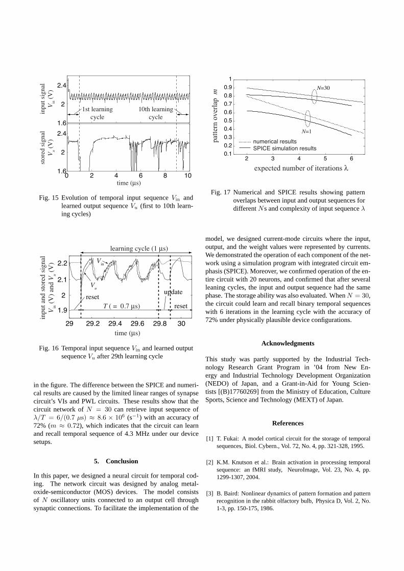
in the figure. The difference between the SPICE and numeri-cal results are caused by the limited linear ranges of synapsecircuit’s VIs and PWL circuits. These results show that thecircuit network ofN = 30 can retrieve input sequence ofλ/T = 6/(0.7 µs) ≈ 8.6 × 10⁶ (s−1) with an accuracy of72% (m ≈ 0.72), which indicates that the circuit can learnand recall temporal sequence of 4.3 MHz under our devicesetups.
5. Conclusion
In this paper, we designed a neural circuit for temporal cod-ing. The network circuit was designed by analog metal-oxide-semiconductor (MOS) devices. The model consistsof N oscillatory units connected to an output cell throughsynaptic connections. To facilitate the implementation of the
N=30
N=1
expected number of iterations λ
pat
tern
over
lap m
0.1
0.2
0.3
0.4
0.5
0.6
0.7
0.8
0.9
1
2 3 4 5 6
numerical results
SPICE simulation results
Fig. 17 Numerical and SPICE results showing patternoverlaps between input and output sequences fordifferentNs and complexity of input sequenceλ
model, we designed current-mode circuits where the input,output, and the weight values were represented by currents.We demonstrated the operation of each component of the net-work using a simulation program with integrated circuit em-phasis (SPICE). Moreover, we confirmed operation of the en-tire circuit with 20 neurons, and confirmed that after severalleaning cycles, the input and output sequence had the samephase. The storage ability was also evaluated. WhenN = 30,the circuit could learn and recall binary temporal sequenceswith 6 iterations in the learning cycle with the accuracy of72% under physically plausible device configurations.
Acknowledgments
This study was partly supported by the Industrial Tech-nology Research Grant Program in ’04 from New En-ergy and Industrial Technology Development Organization(NEDO) of Japan, and a Grant-in-Aid for Young Scien-tists [(B)17760269] from the Ministry of Education, CultureSports, Science and Technology (MEXT) of Japan.
References
[1] T. Fukai: A model cortical circuit for the storage of temporalsequences, Biol. Cybern., Vol. 72, No. 4, pp. 321-328, 1995.
[2] K.M. Knutson et al.: Brain activation in processing temporalsequence: an fMRI study, NeuroImage, Vol. 23, No. 4, pp.1299-1307, 2004.
[3] B. Baird: Nonlinear dynamics of pattern formation and patternrecognition in the rabbit olfactory bulb, Physica D, Vol. 2, No.1-3, pp. 150-175, 1986.

[4] W.J. Freeman: Why neural networks don’t get fly: inquiry intothe neurodynamics of biological intelligence, Proc. IEEE Int.Conf. Neural Networks, Vol. 2, pp. 1-7, 1988.
[5] D.L. Wang: Temporal pattern processing, Handbook of BrainTheory and Neural Networks, MIT Press, pp. 967-971, 1995.
[6] A.R. Aluizo and G.A. Barreto: Context in temporal sequenceprocessing: A self-organizing approach and its application torobotics, IEEE Trans. Neural Networks, Vol. 13, No. 1, pp.45-57, 2002.
[7] S.C. Liu and R. Douglas: Temporal coding in a silicon networkof integrated and fire neurons, IEEE Trans. Neural Networks,Vol. 15, No. 5, pp. 1305-1314, 2004.
[8] H.H. Ali and M.E. Zaghloul: VLSI implementation of an asso-ciative memory using temporal relations, Proc. IEEE Int. Symp.Circuit and Syst., pp. 1877-1880, 1993.
[9] J.L. Walsh, et. al.: A close set of orthogonal functions, Amer.J. Math., Vol. 45, No. 1, pp. 5-24, 1923.
[10] H.R. Wilson and J.D. Cowan: Excitatory and inhibitory inter-actions in localized populations of model neurons, Biophys. J.,Vol. 12, pp. 1-24, 1972.
Gessyca Maria Tovar was born inVenezuela in 1981. She received the B.S.degree in electronic engineering fromJose Antonio Paez University, Venezuela,in 2004, and the M.S. degree fromHokkaido University, Hokkaido, Japan,in 2008. Currently she is working to-wards her Doctor degree in the De-partment of Electrical Engineering atHokkaido University, Japan. Her re-search interests include neuromorphic
computation and hardware implementation. She is a student mem-ber of the INNS.was born in Venezuela in 1981. She receivedthe B.S. degree in Electronic was born in Venezuela in 1981
Tetsuya Asai is an Associate Profes-sor in the Graduate School of Informa-tion Science and Technology, HokkaidoUniversity, Sapporo, Japan. His re-search interests concentrate around de-veloping nature-inspired integrated cir-cuits and their computational applica-tions. Current topics that he is involvedwith include; intelligent image sensorsthat incorporate biological visual sys-tems or cellular automata in the chip,neuro chips that implement neural ele-
ments (neurons, synapses, etc.) and neuromorphic networks, andreaction-diffusion chips that imitate vital chemical systems.
Daichi Fujita was born in Yamaguchi,Japan, in 1985. He received the B.S.degree in electrical engineering fromHokkaido University, Hokkaido, Japan,in 2008. Currently he is working towardshis Master degree in the Department ofElectronic for Informatics at HokkaidoUniversity, Japan. His research interestsinclude neuromorphic computation andhardware implementation. He is a stu-dent member of the IEICE.was born in
Venezuela in 1981. She received the B.S. degree in Electron-icShe received the B.S. degree in ElectronicShe received theB.S. degree in Electronic was born in Venezuela in 1981
Yoshihito Amemiya received the B.E.,M.E., and Ph.D. degrees from the TokyoInstitute of Technology, Tokyo, Japan, in1970, 1972, and 1975. He joined NTTMusashino Laboratories in 1975, wherehe worked on the development of siliconprocess technologies for high-speed logicLSIs. From 1983 to 1993, he was withNTT Atsugi Laboratories and developedbipolar and CMOS circuits for Booleanlogic LSIs, neural network LSIs, and cel-
lular automaton LSIs. Since 1993, he has been a Professor of theDepartment of Electrical Engineering, Hokkaido University, Sap-poro. His research interests are in the fields of silicon LSI circuits,signal processing devices based on nonlinear analog computation,logic systems consisting of single-electron circuits, and information-processing devices making use of quantum nanostructures.
(Received June 9, 2008; revised September 16, 2008)