analog circuits and systems - nptelnptel.ac.in/courses/117108107/lecture 20.pdf · analog circuits...
TRANSCRIPT
Analog Circuits and Systems Prof. K Radhakrishna Rao
Lecture 20: DC Voltage Regulators
1

Review
2

DC Voltage Power Supply
3
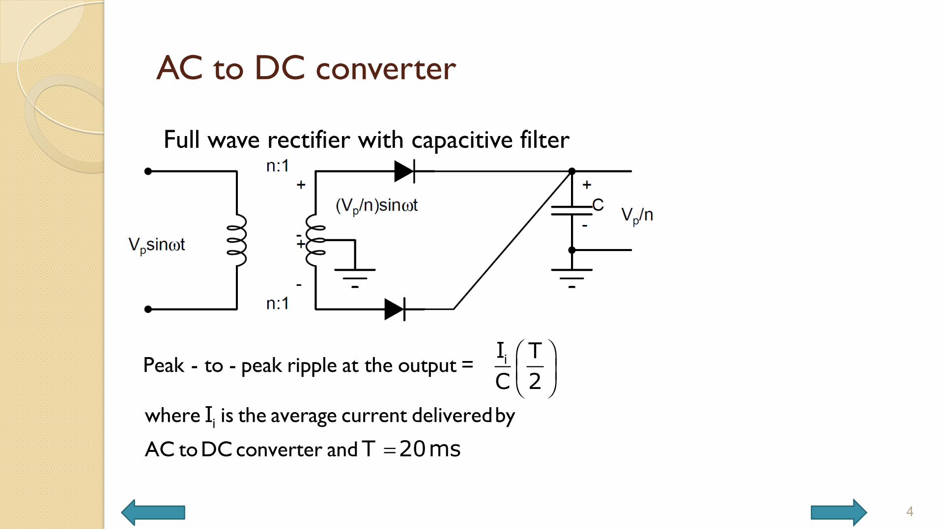
AC to DC converter
Full wave rectifier with capacitive filter
4
i
i
I T C 2
IT 20ms
⎛ ⎞⎜ ⎟⎝ ⎠
=
Peak - to - peak ripple at the output =
where is the average current deliveredby
AC toDC converter and
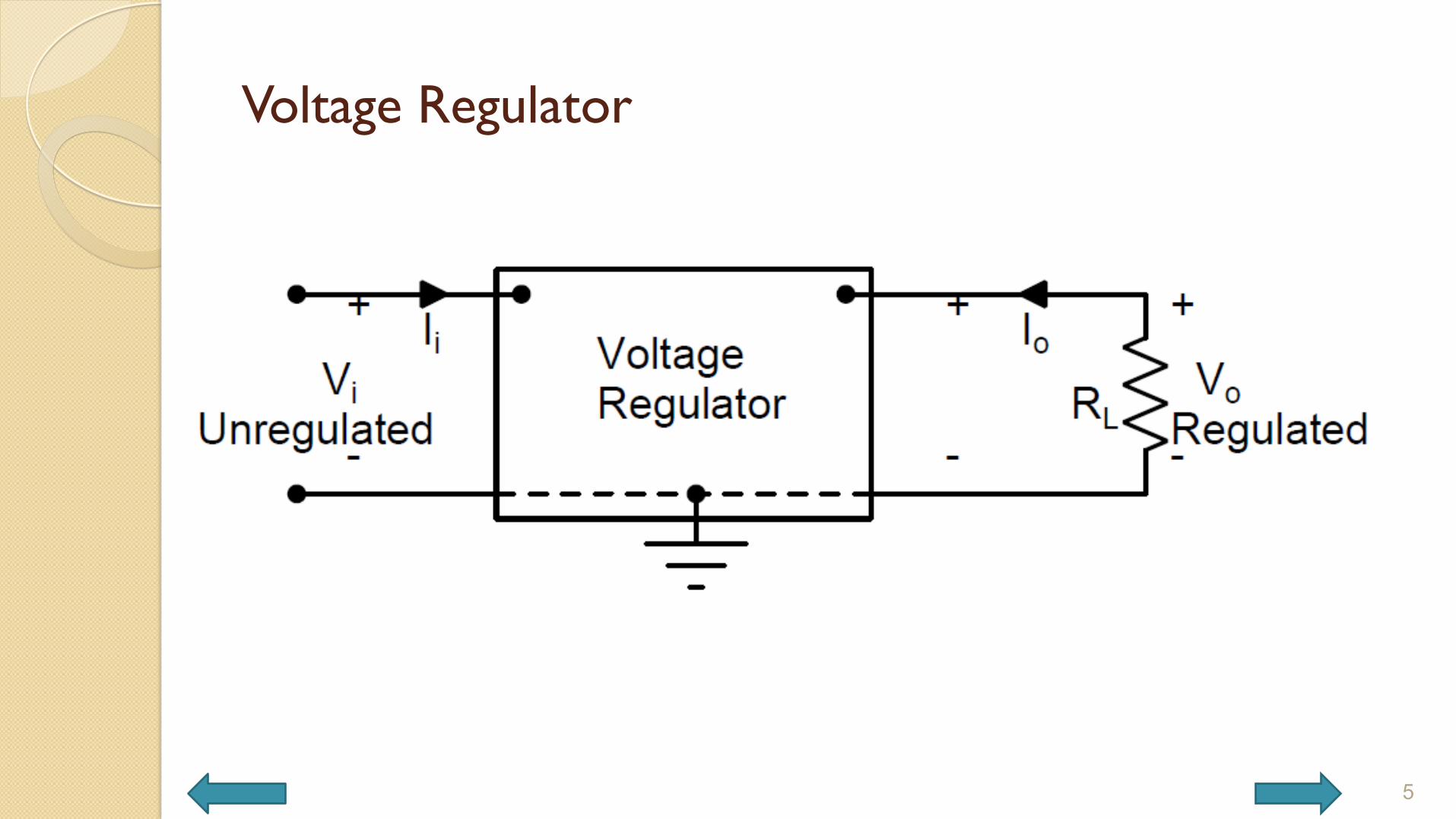
Voltage Regulator
5
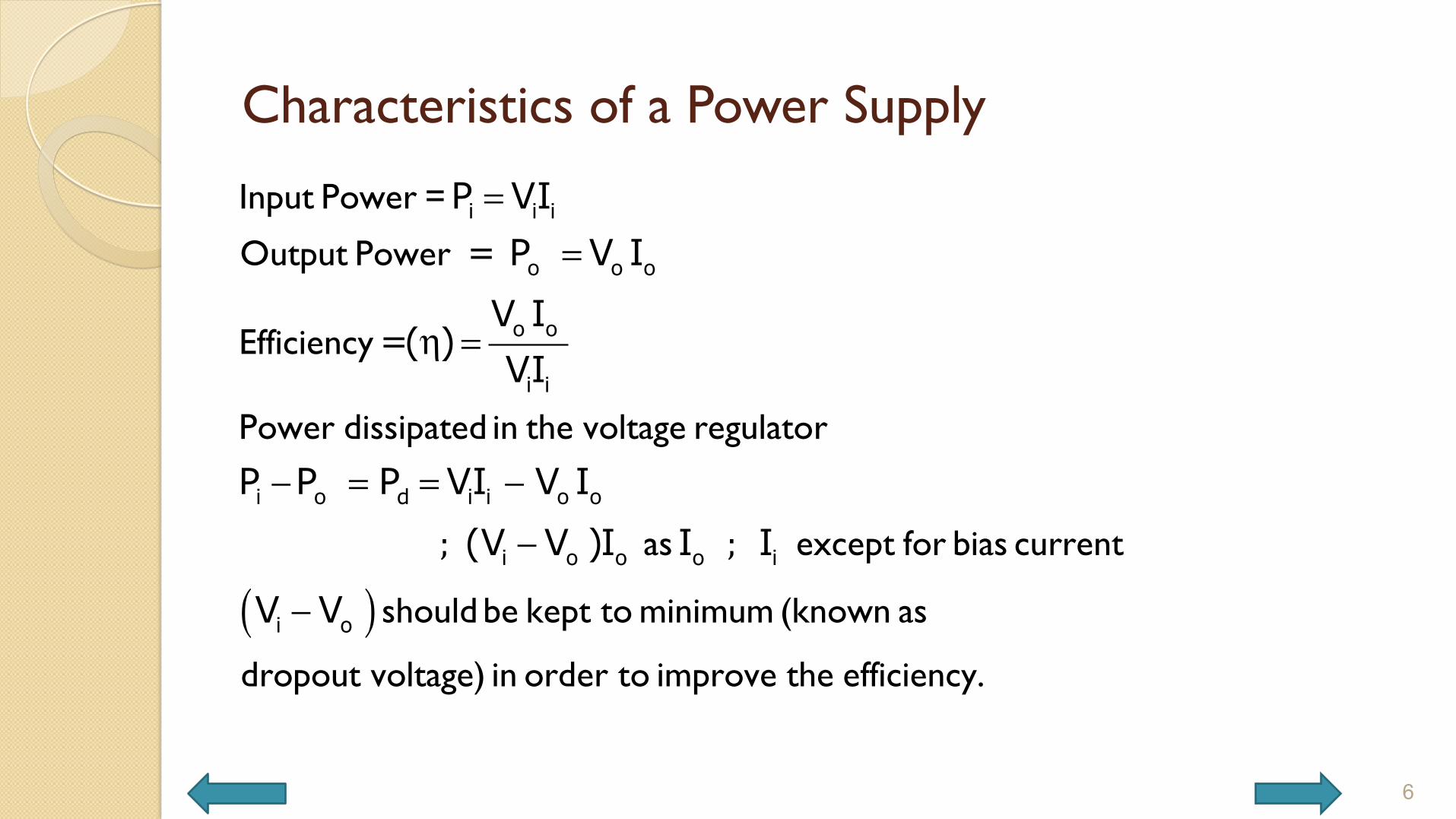
Characteristics of a Power Supply
6
( )
==
η =
− = = −
−
−
; ;
i i i
o o o
o o
i i
i o d i i o o
i o o o i
i o
P VI = P V I
V I=( )
VI
P P P VI V I(V V )I I I
V V
Input Power =
Output Power
Efficiency
Power dissipated in the voltage regulator
as except for bias current
should be kept to minimum (known as
dropout voltage) in order to improve the efficiency.

Characteristics of a Power Supply (contd.,)
7
100∂
o i
o
o
o o
V VVx
VV I
Line regulation : Percentage change in as the input voltage changes
from its maximum to minimum
Load regulation : Percentage change in as the output current
is changed from its mini 100∂ o
o
Vx
Vmum to maximum
Temperature coefficient of the output voltage : Change in output voltage
for a small change in input voltage at a specified output voltage
expressed in terms of parts per millio( )∂ ∂
°o
o
V / Tppm/ C
Vn =
Characteristics of a Power Supply (contd.,)
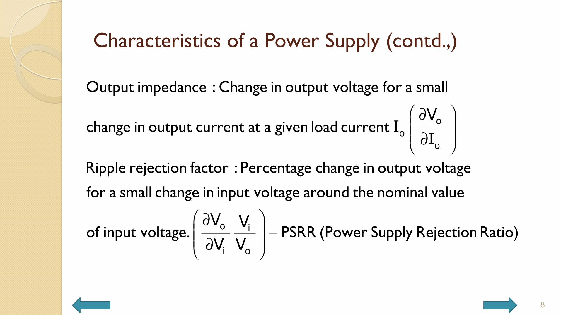
8
⎛ ⎞∂⎜ ⎟⎜ ⎟∂⎝ ⎠
oo
o
VI
I
Output impedance : Change in output voltage for a small
change in output current at a given load current
Ripple rejection factor : Percentage change in output voltage
for a small change
⎛ ⎞∂−⎜ ⎟⎜ ⎟∂⎝ ⎠
o i
i o
V VV V
in input voltage around the nominal value
of input voltage. PSRR (Power Supply Rejection Ratio)
Load/Line Transient Regulation
� Voltage at the output terminal is likely to have undesirable transients at the time of switching on the input power or when step load changes occur
� The output impedance of the voltage regulator is complex � The presence of feedback loop with large loop gain and the multiple
poles associated with this loop makes the output impedance complex
� Compensation has to be provided to make the output impedance resistive
9
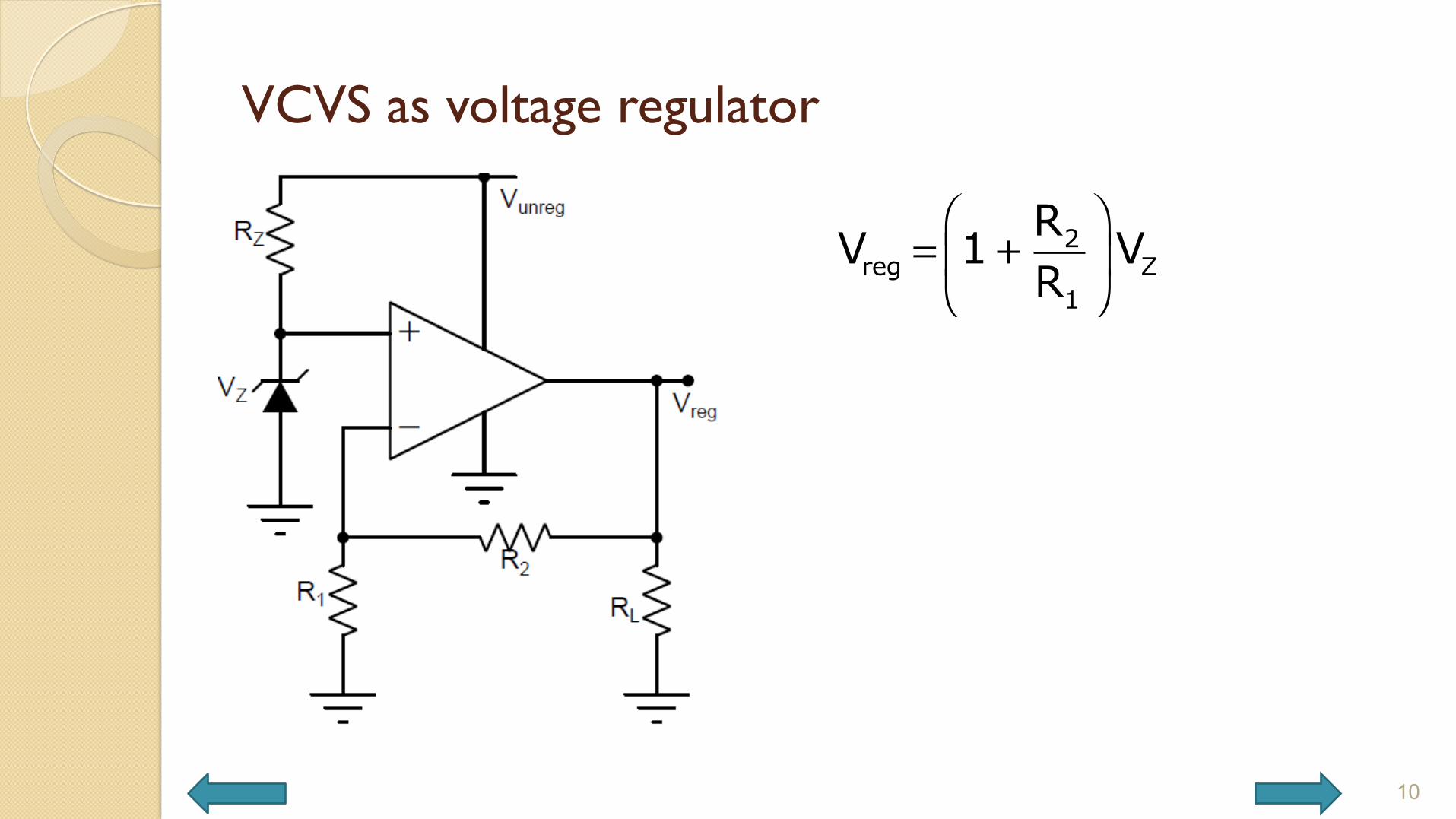
VCVS as voltage regulator
10
2reg Z
1
RV 1 VR
⎛ ⎞= +⎜ ⎟⎝ ⎠
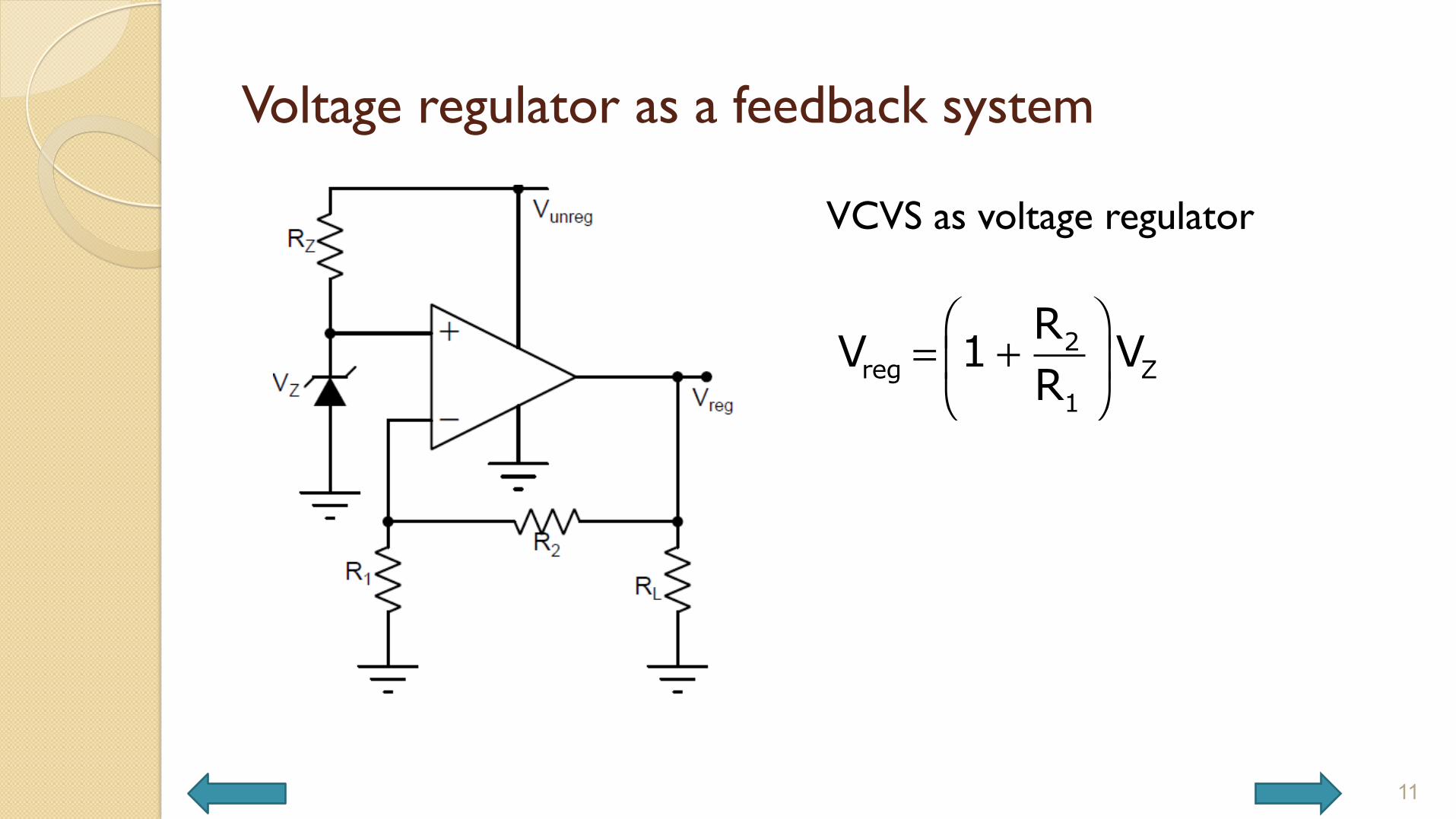
Voltage regulator as a feedback system
11
2reg Z
1
RV 1 VR
⎛ ⎞= +⎜ ⎟⎝ ⎠
VCVS as voltage regulator

Voltage regulator as a feedback system (contd.,)
12
10 10 11 1 2
1 2 2
21
10
1
2
12
1 2
G GG =s s s1 1 s 1
GGBGss 1
RGR R
ωω <<ω
⎛ ⎞ ⎛ ⎞ ⎛ ⎞+ + +⎜ ⎟ ⎜ ⎟ ⎜ ⎟ω ω ω⎝ ⎠ ⎝ ⎠ ⎝ ⎠
ωω
⎛ ⎞+⎜ ⎟ω⎝ ⎠
+
;
;
;
;
Forward path for
In internally compensated Op Amps
Hence
Feedback path
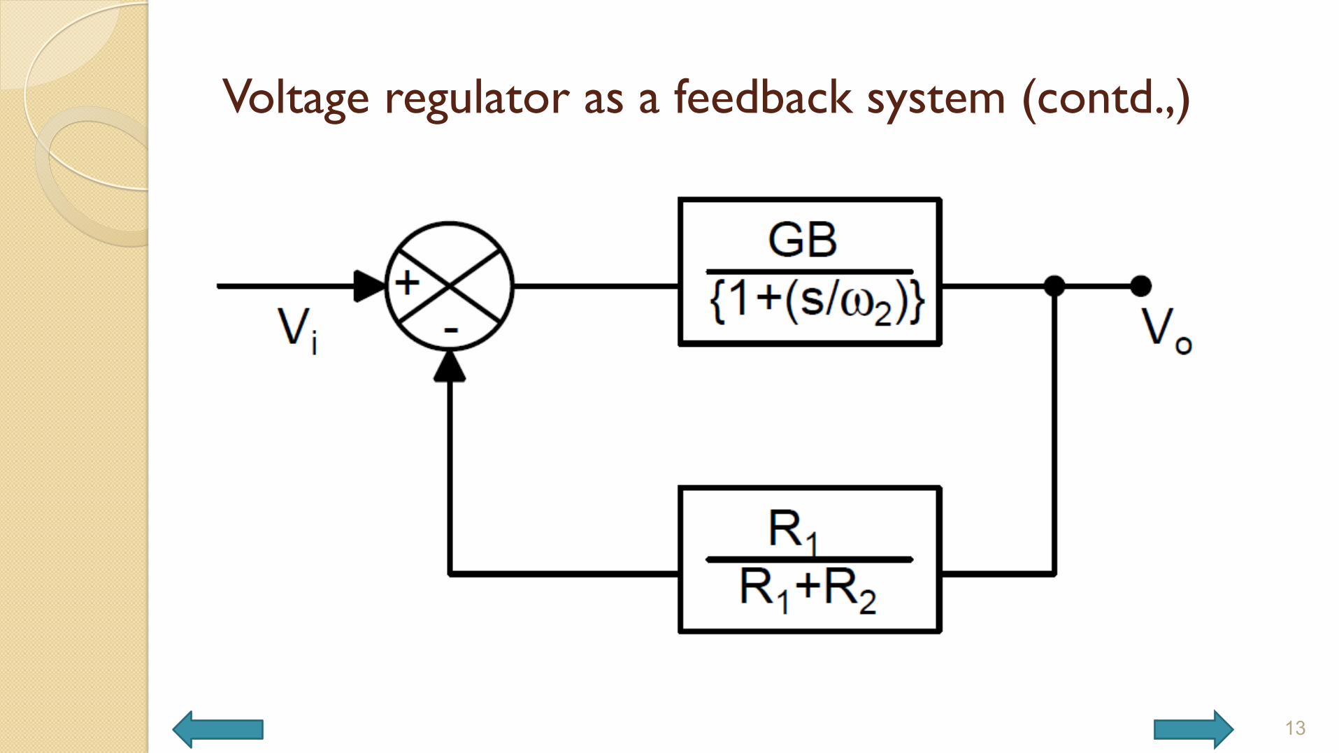
Voltage regulator as a feedback system (contd.,)
13

Voltage regulator as a feedback system (contd.,)
14
2
1
2 2 2
1 1 1
22 2 2
1 1 1
2 2
2
12
22 2
1
1
1 1 1
11 1 1 11 1 1
1
1 1
⎛ ⎞+⎜ ⎟
⎝ ⎠⎛ ⎞ ⎛ ⎞ ⎛ ⎞
+ + +⎜ ⎟ ⎜ ⎟ ⎜ ⎟⎝ ⎠ ⎝ ⎠ ⎝ ⎠= = =⎛ ⎞ ⎛ ⎞ ⎛ ⎞ ⎛ ⎞
+ + + +⎜ ⎟ ⎜ ⎟ ⎜ ⎟ ⎜ ⎟⎛ ⎞⎝ ⎠ ⎝ ⎠ ⎝ ⎠ ⎝ ⎠+ + + +⎜ ⎟ω ω⎝ ⎠⎛ ⎞
+⎜ ⎟⎝ ⎠= =
⎛ ⎞+ + + ω⎜ ⎟ω ω ⎝ ⎠
o
i
o
i
l
n n
V RV R
R R RR R RV
V R R Rs s sg R R Rs
GB GB GB
RR GBwhere Qs s RQ R
;

Voltage regulator as a feedback system (contd.,)
15
� High rate of rise and least amount of ringing occurs at Q = 1 � is determined by the required output voltage
� As w2 and G10 are fixed for a given Op Amp w1 is chosen to make Q = 1
� In internally compensated Op Amps like 741 and TL081 w1 is already chosen to make Q = 1 for Vo = VZ, i.e., G2 = 1
= =+
Z 12
o 1 2
V RGV R R
2 21
10 1
R1G R
⎛ ⎞ωω = +⎜ ⎟
⎝ ⎠
21
10Gω
ω =
Voltage regulator as a feedback system (contd.,)
16
� For any other G2 < 1; Q will always be correspondingly less than1resulting in unsatisfactory transient response.
� It is therefore necessary to use uncompensated Op Amps like LM748 to design voltage regulators with good transient response.
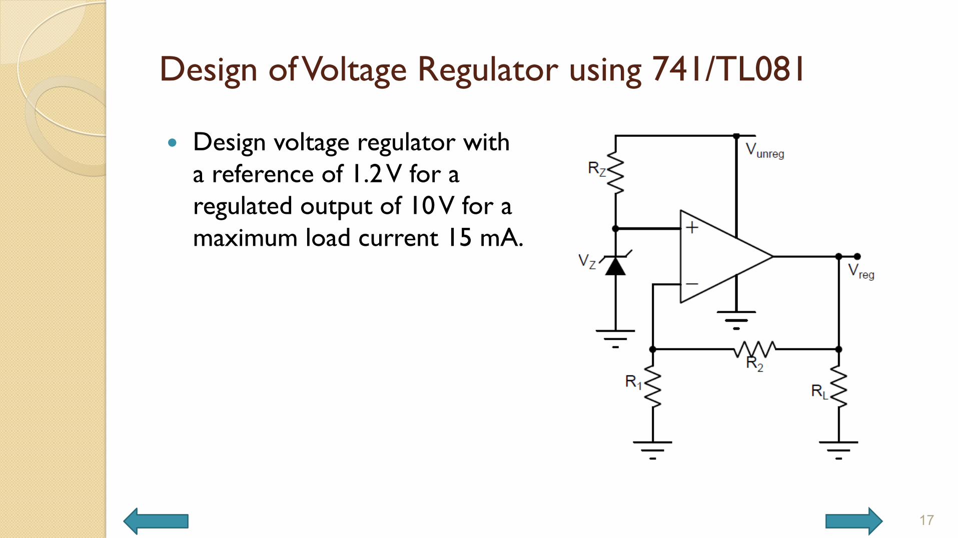
Design of Voltage Regulator using 741/TL081
� Design voltage regulator with a reference of 1.2 V for a regulated output of 10 V for a maximum load current 15 mA.
17

Design of Voltage Regulator using 741/TL081 (contd.,)
� Voltage Regulator using Voltage reference IC for 1.2 V: REF3012
18
1
2
1
2
R1 10 1.2VR
R = 1.2 k and R = 8.8 k
⎛ ⎞+ =⎜ ⎟
⎝ ⎠ΩΩ
The Op Amp used is 741

Simulation
19

Simulation
20
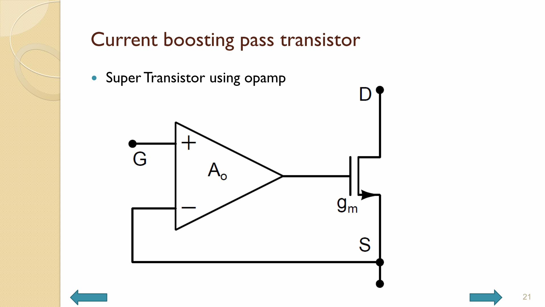
Current boosting pass transistor
� Super Transistor using opamp
21

Current boosting pass transistor (contd.,)
� using n-channel pass transistor � using p-channel pass transistor - Load Dropout Regulator (LDO)
22
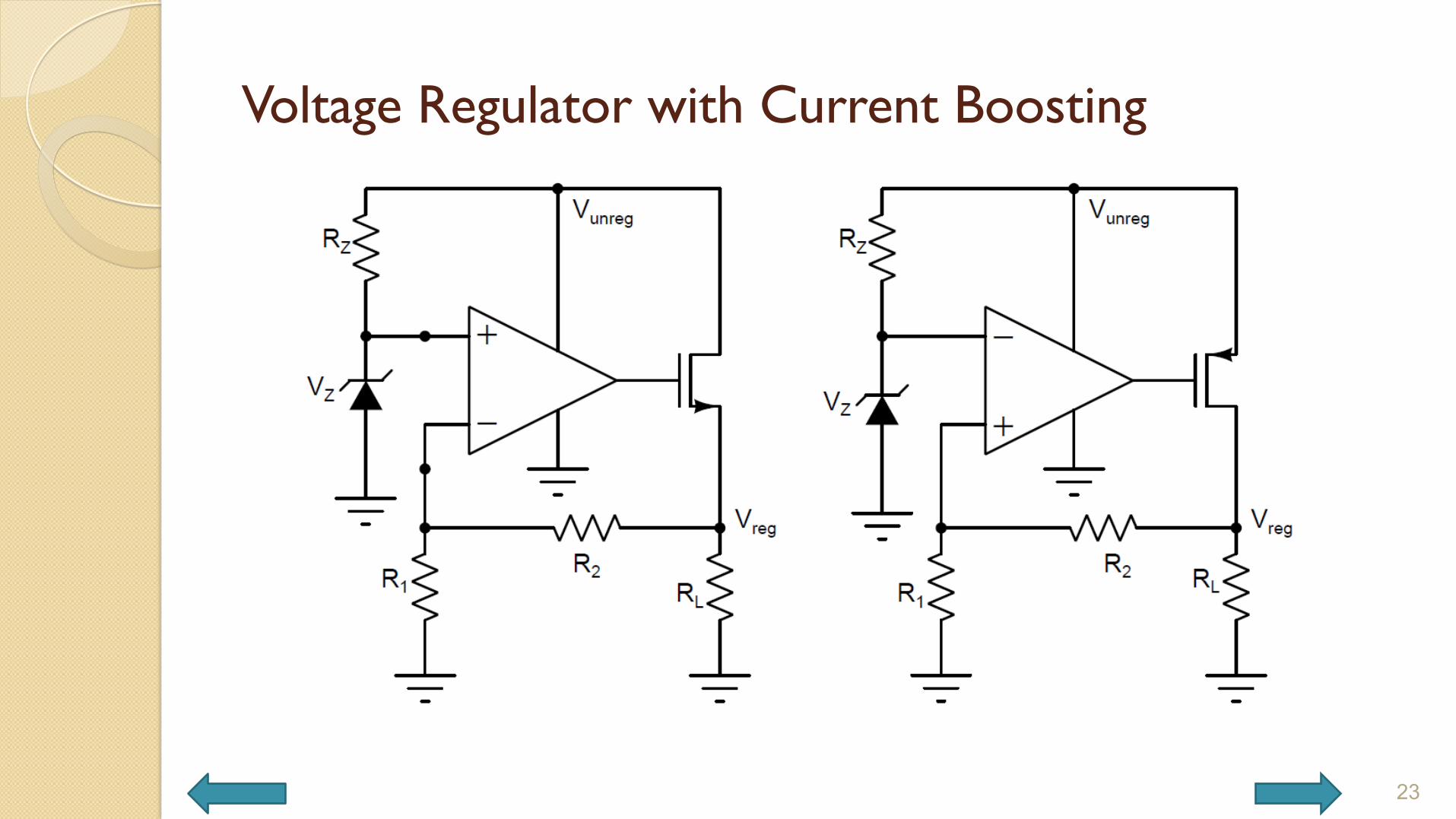
Voltage Regulator with Current Boosting
23
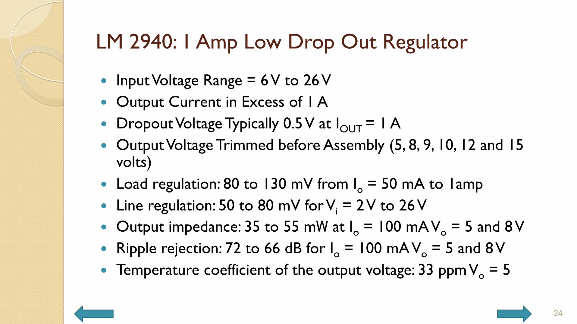
LM 2940: 1 Amp Low Drop Out Regulator
� Input Voltage Range = 6 V to 26 V � Output Current in Excess of 1 A � Dropout Voltage Typically 0.5 V at IOUT = 1 A � Output Voltage Trimmed before Assembly (5, 8, 9, 10, 12 and 15
volts) � Load regulation: 80 to 130 mV from Io = 50 mA to 1amp � Line regulation: 50 to 80 mV for Vi = 2 V to 26 V � Output impedance: 35 to 55 mW at Io = 100 mA Vo = 5 and 8 V � Ripple rejection: 72 to 66 dB for Io = 100 mA Vo = 5 and 8 V � Temperature coefficient of the output voltage: 33 ppm Vo = 5
24
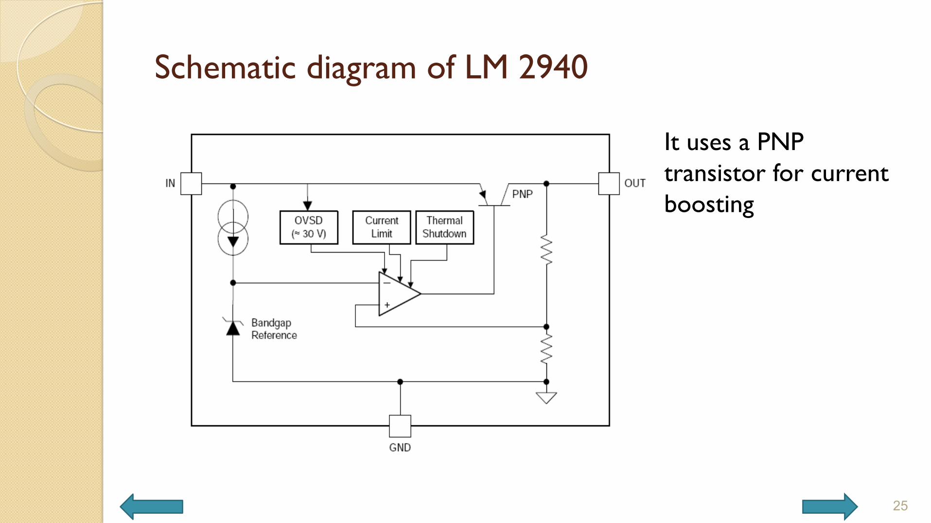
Schematic diagram of LM 2940
25
It uses a PNP transistor for current boosting

Using LM2940
* C1 is needed if regulator is located far (more than a few inches) from power supply filter
** COUT must be at least 22 μF to maintain stability. It may be increased without bound to maintain regulation during transients. Locate as close as possible to the regulator. This capacitor must be rated over the same operating temperature range as the regulator and the ESR (Equivalent Series Resistance) is critical.
26

Conclusion
27