analog (and discrete-time) integrated circuits · bits for control of the dac switches. (a ......
TRANSCRIPT

Lecture 10, ATIKData converters 3

What did we do last time?
A quick glance at sigma-delta modulators
Understanding how the noise is shaped to higher frequencies
DACs
A case study of the current-steering DAC architecture.
Suggesting some common implementation and architectural details
Impact of impedance
Impact of mismatch
Some extras needed
2012-02-27::ANTIK_0025 (P10A) Analog (and discrete-time) integrated circuits 289 of 561

What will we do today?
Case-study pipelined ADC
Architecture and a general overview
Error correction techniques
Sample-and-hold design
Comparator design
Wrap-up
2012-02-27::ANTIK_0025 (P10A) Analog (and discrete-time) integrated circuits 290 of 561
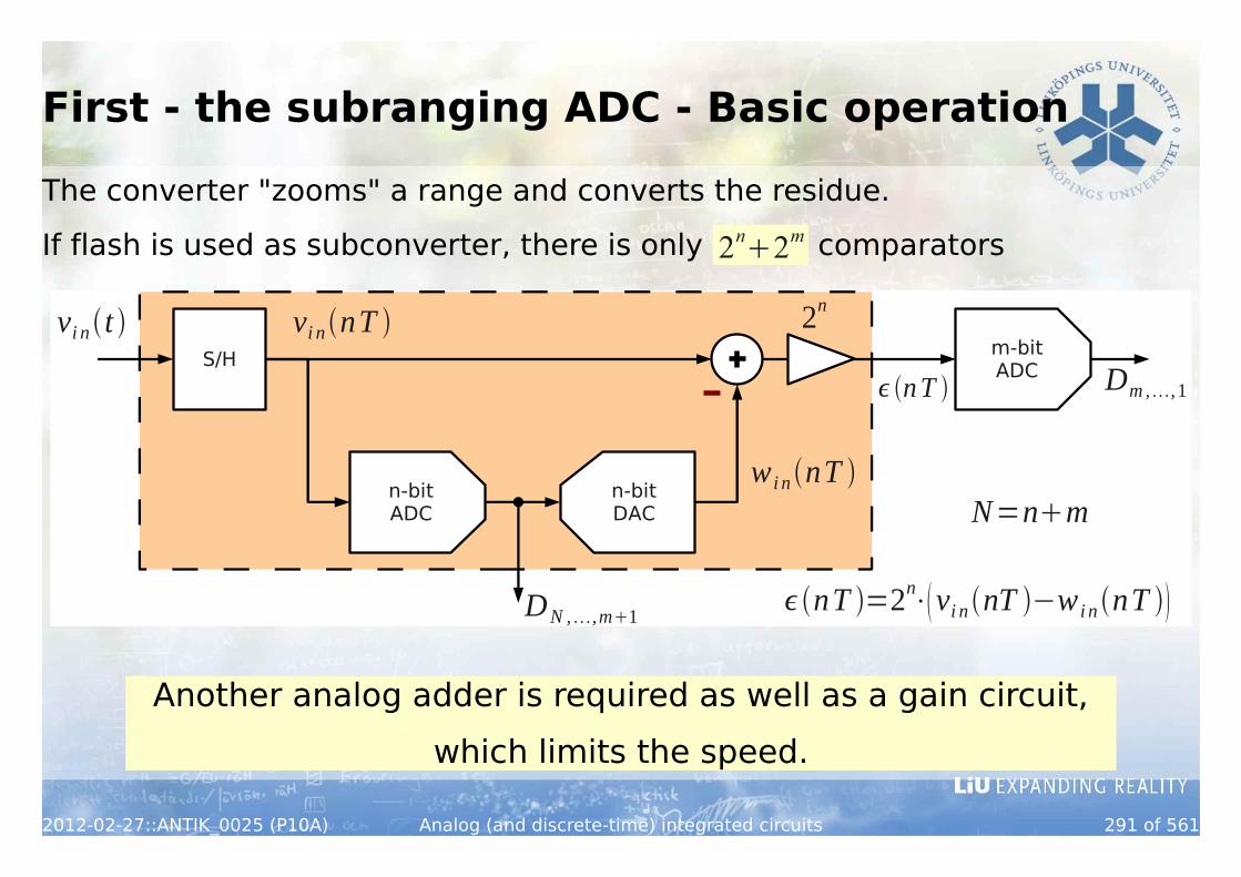
First - the subranging ADC - Basic operation
The converter "zooms" a range and converts the residue.
If flash is used as subconverter, there is only 2n2m comparators
Another analog adder is required as well as a gain circuit,
which limits the speed.
2012-02-27::ANTIK_0025 (P10A) Analog (and discrete-time) integrated circuits 291 of 561
n-bit ADC
S/H
n-bit DAC
m-bit ADC
vi nt
Dm,,1
DN ,,m1
2nvi nnT
w i nnT
N=nm
nT
nT =2n⋅vi nnT −w i nnT

Pipelined ADC in one picture
Multiple subranging ADC in series
A series of refinements, zoom-ins, of the convertible range
Assume same range in each stage
2012-02-27::ANTIK_0025 (P10A) Analog (and discrete-time) integrated circuits 292 of 561
00
vi nt 1nT
01
10
11
vref
0
00
01
10
11
00
01
10
11
00
01
10
11
vi n
1
10 01 00 11
2nT 3nT 4 nT

Pipelined ADC - delays
Balance the delays and "cleverly" distribute the clock to avoid race
A pipelined ADC will have longer latency
2012-02-27::ANTIK_0025 (P10A) Analog (and discrete-time) integrated circuits 293 of 561
vi nt
10
01
00
11T T T
T T
T
T T T T
Clock direction to avoid race

Pipelined ADC - sensitive towards errors
Any misinterpreted level quickly diverges and never recovers!
Overlap can be digitally corrected (without training!)
2012-02-27::ANTIK_0025 (P10A) Analog (and discrete-time) integrated circuits 294 of 561
00
01
10
11
vref
0
00
01
10
11
00
01
10
11
00
01
10
11
vi n

Pipelined ADC - error correction
Increase the number of stages and reduce overlap, i.e., decrease the scaling factor, 2n . Now, less likely to diverge and is able to recover.
More stages are required, but typically worth it
2012-02-27::ANTIK_0025 (P10A) Analog (and discrete-time) integrated circuits 295 of 561
00
01
10
11
vref
0
00
01
10
11
00
01
10
11
00
01
10
11
vi n

Pipelined ADC - error correction cont'd
Trivial circuitry to retrieve the most likely code!
2012-02-27::ANTIK_0025 (P10A) Analog (and discrete-time) integrated circuits 296 of 561
00
vi nt
01
10
11
vref
0
00
01
10
11
00
01
10
11
00
01
10
11
vi n
01 10 00 01
0
0
10
01
1
0
00
00
1
1

PADC: Taking a look at the subcomponents
Sample-and-hold
Sub-ADC
Sub-DAC
Adder
Multiplier
2012-02-27::ANTIK_0025 (P10A) Analog (and discrete-time) integrated circuits 297 of 561
n-bit ADC
S/H
n-bit DAC
vi nt
DN ,,m1
2nvi nnT
w i nnT
nT

Sample-and-hold process
The input should be sampled and held to reduce the jitter in the subcomponents.
Inherent delays will otherwise cause mismatch.
Jitter (interdelay) is a very strong limitation on obtainable performance
S/H at input of ADC must have full accuracy !!!
2012-02-27::ANTIK_0025 (P10A) Analog (and discrete-time) integrated circuits 298 of 561
t=nT
a nT a t

Sample-and-hold, 1st-level implementation
Passive sampling
Limitations
Clock-feedthrough
Charge-injection
On-resistance
Distortion
Jitter
Noise
2012-02-27::ANTIK_0025 (P10A) Analog (and discrete-time) integrated circuits 299 of 561
CH
v2nT v1t
t

Sample-and-hold charge injection
Channel charge injection
V 2nT ~W L⋅C ox⋅V −V T−V 2nT
C H
Large capacitor is good!
Force the delta voltage to always be lower than the LSB voltage:
V ref⋅W⋅L⋅C ox
2C H
2⇒W⋅L
C H
Cox⋅2N1
2012-02-27::ANTIK_0025 (P10A) Analog (and discrete-time) integrated circuits 300 of 561
CH
v2nT v1t
t

Sample-and-hold clock feedthrough
Clock feed-through
V 2nT =C ol
CH
⋅V −V 2nT
such that
V 2 nT =V 1nT ⋅1C ol
CH−C ol
CH
⋅V T
Large capacitor is good!
Force the delta voltage to always be lower than the LSB voltage:
V ref⋅Col
C H
2⇒C ol
C H
2N1
2012-02-27::ANTIK_0025 (P10A) Analog (and discrete-time) integrated circuits 301 of 561
CH
v2nT v1t
t

Sample-and-hold bandwidth
Non-zero resistance
Gon=⋅V phi−V T−V 1nT
Bandwidth limitation, but also distortion due to signal-dependent resistance
Large capacitor is bad!
For a full-scale step at the input, we should settle within 1 LSB accuracy, i.e.
V ref⋅e−Gon
2CH⋅ f s2⇒−
Gon
2CH⋅f s
−ln 2N1⇒Ron≪
0.5⋅ln 2C H⋅ f s⋅N1
2012-02-27::ANTIK_0025 (P10A) Analog (and discrete-time) integrated circuits 302 of 561
CH
v2nT v1t
t

Noise
Given by the bandwidth and the brickwall pole
vn , tot2 =
k TCH
Large capacitor is good!
Quantization noise should be larger than noise, i.e.
vn , tot2
2
12⇒C H12 k T⋅
22N
V ref2
2012-02-27::ANTIK_0025 (P10A) Analog (and discrete-time) integrated circuits 303 of 561
CH
v2nT v1t
t

Sub-ADC
Most likely a flash ADC
Fastest and best choice for low number of bits
Use a resistive divider to create reference voltages
Offset and matching of resistors must match the accuracy of the active pipeline stage
Mismatch information will give requirements on transistors and resistor sizes
Relative error is inversely dependent on the area
2012-02-27::ANTIK_0025 (P10A) Analog (and discrete-time) integrated circuits 304 of 561
V ref
R r
R r
R r
R r
V i n

Sub-DAC
Reuse the resistive divider for the sub DAC!
Notice that the picture does not display the correct decoding of the t_i bits for control of the DAC switches. (A thermometer-to-walking-one converter consisting of a bank of XOR gates is needed.)
2012-02-27::ANTIK_0025 (P10A) Analog (and discrete-time) integrated circuits 305 of 561
V ref
Rr
Rr
Rr
Rr
V i nnT
w nT
t1n
t 2n
t 3n
t 4n
tM n

Adder/gain
A rather compact design can be obtained reusing and combining difference active and passive components.
2012-02-27::ANTIK_0025 (P10A) Analog (and discrete-time) integrated circuits 306 of 561
V ref
R r
R r
R r
R r
V i nnT
−w nT
t1n
t 2n
t 3n
t 4n
tM n
Encoding not shown
R
R
2n R
−nT
By flipping the t_k bits, we can create the negative version of w(nT) (!)
Inversion at the output is no issue, since we can reorder the comparators in the next stage.

Resistance is futile...
Why?
Noise and OTA design
Go for capacitor-based circuits
Switched-capacitor comparators in the sub ADC
Switched-capacitor DAC
Switched-capacitor summation and multiplier
2012-02-27::ANTIK_0025 (P10A) Analog (and discrete-time) integrated circuits 307 of 561
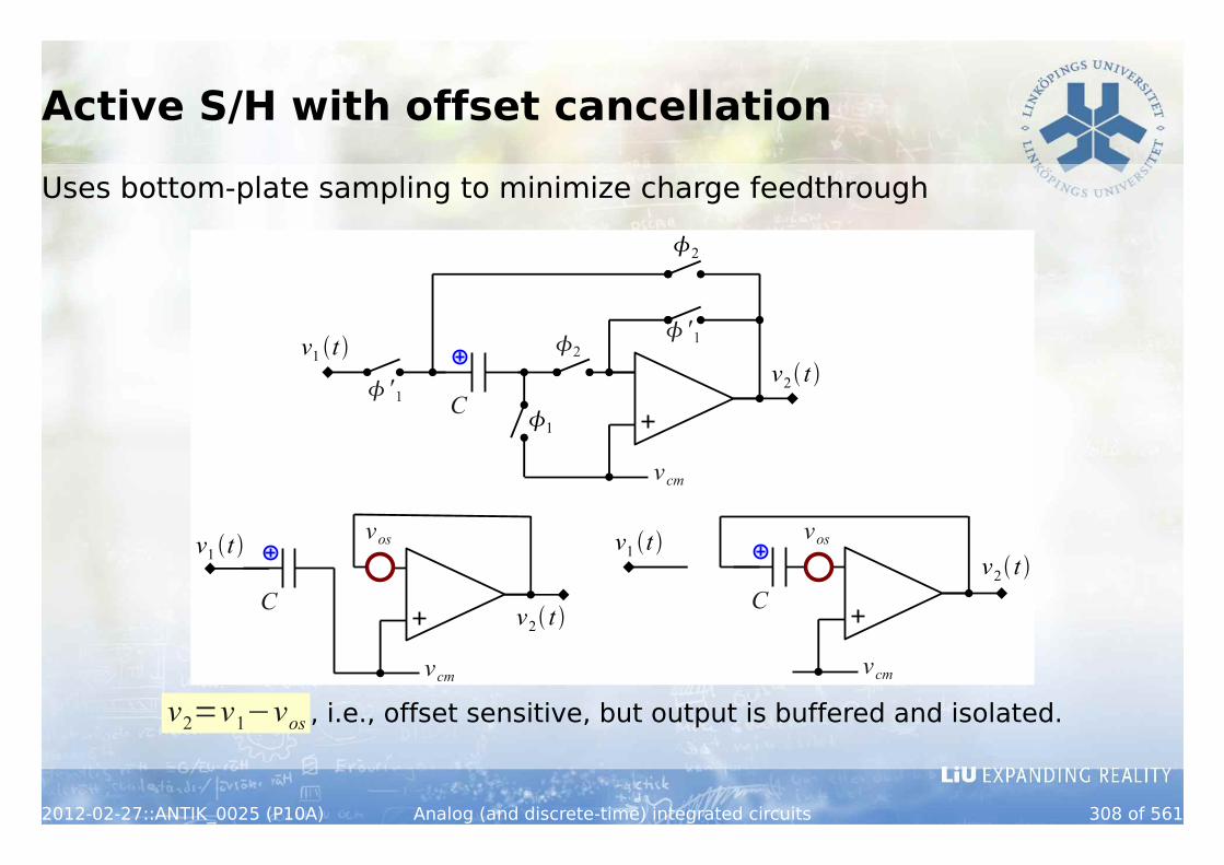
Active S/H with offset cancellation
Uses bottom-plate sampling to minimize charge feedthrough
v2=v1−vos , i.e., offset sensitive, but output is buffered and isolated.
2012-02-27::ANTIK_0025 (P10A) Analog (and discrete-time) integrated circuits 308 of 561
v1 t v2 t
2
'1
' 1 C1
2
v1 t
v2 t C
vcm
vcm
v2 t C
vcm
v1 t vosvos

Comparators
A comparator is not an OP! Consider speed vs. gain
A s=A0
1s / p1⇒=
1p1≈
A0ug
vs three-stage example
A ' s =A' 0
3
1s / p' 1 3⇒ '=3⋅
1p ' 1
=3 A'0ug
, with A '0=A01 /3
'=⋅3 A' 0A0
=⋅3
A02 /3
(Phase margin is not necessarily an issue!)
2012-02-27::ANTIK_0025 (P10A) Analog (and discrete-time) integrated circuits 309 of 561
V i nV o ut

Comparators, speed vs resolution 1
Characteristic resolution parameter, c_r, is the smallest level that can toggle the output to reliable levels
V OH−V OL=A0⋅V IH−V IL ⇒cr=V OH−V OL
A0
Assume a first-order system and apply an input step:
vout t =V OLA0⋅v step⋅1−e−c t
Apply the smallest possible signal
vout t =V OLA0⋅cr⋅1−e−c t =V OLV OH−V OL ⋅1−e−c t
Check when we pass the mid-level at the output
vout =V OLV OH−V OL
2=V OLV OH−V OL ⋅1−e−c ⇒0.5=1−e−c⇒=
ln 2c
2012-02-27::ANTIK_0025 (P10A) Analog (and discrete-time) integrated circuits 310 of 561

Comparators, speed vs resolution 2
Assume now that the input step is K times larger:
vout ' =V OLV OH−V OL
2=V OL V OH−V OL ⋅K⋅1−e−c ' ⇒
0.5=K⋅1−e−c ' ⇒ '=1c
⋅ln2K2K−1
⇒ '=⋅
ln2K2K−1ln 2
≈
2 K⋅ln 2
If K goes towards infinity, the delay goes towards 0.
The more accuracy, the lower sample frequency!
2012-02-27::ANTIK_0025 (P10A) Analog (and discrete-time) integrated circuits 311 of 561

Comparators, offset "cancellation" 1
The sub ADC takes sampled input and reference at two different phases:
First reference is selected
q ref =C⋅V ref ,k−V 2 ref
where
V 2ref =vos⋅A
1A
Then signal is selected and charge must be preserved
q i n=C⋅v i ni n−v osV 2i n
A =q ref =C⋅V ref ,k−vos⋅A1A
V 2 i n=−A⋅v i ni n−V ref , k vos⋅A1A
(no amplified offset)
2012-02-27::ANTIK_0025 (P10A) Analog (and discrete-time) integrated circuits 312 of 561
v i nnT v2 t
ref
i nC
vos
V ref , k
ref

Comparators, offset cancellation in OTA
Correlated double sampling
First phase
q1=C1⋅v1−v os q2=C 2⋅0−vos
Second phase
q1=−C1⋅vosq2=C 2⋅v2−vos
Total charge is preserved
C1⋅v1−vos −C 2⋅vos=−C1⋅v osC 2⋅v2−vos ⇒v2v1=C1
C 2
[OFFSET CANCELLED]
2012-02-27::ANTIK_0025 (P10A) Analog (and discrete-time) integrated circuits 313 of 561
v1 t
v2 t
1
1
C1
2
2
vos
1C 2

Comparators, structure
Use (low-gain) preamplifiers and then high-speed positive-feedback latch, which has infinite (DC) gain (time/gain trade-off)
2012-02-27::ANTIK_0025 (P10A) Analog (and discrete-time) integrated circuits 314 of 561
Preamplifier section of different kindslatch
latch
vout t A1,1 A2,1 Ak ,1
l~gm
C p
, Al=∞
V OL
V OH
v i n
V ref , k

MDAC, concept
Combines the sub-DAC, adder, gain, and sample-and-hold
2012-02-27::ANTIK_0025 (P10A) Analog (and discrete-time) integrated circuits 315 of 561
n-bit ADC
S/H
n-bit DAC
2n
S/H
Combined intoone SC MDAC

MDAC, SC implementation
Bits bi from the ADC (in the 5-bit example below they are binary)
Left as exercise to prove operation ...
2012-02-27::ANTIK_0025 (P10A) Analog (and discrete-time) integrated circuits 316 of 561
k1nT C 0
V r e f
C1C 2C 3C 4C5
b3b4 b2 b1 b0
1
k nT / v i n
1
1
2

Pipelined ADC, conclusions
Compact SC solution
2012-02-27::ANTIK_0025 (P10A) Analog (and discrete-time) integrated circuits 317 of 561
Pipeline stage
v1 t
v2 t
1
1
C1
2
2
vos
1C 2
V ref
Rr
Rr
Rr
Rr
V i nnT
t1n
t 2n
t 3n
t 4n
k1nT C 0
V r e f
C1C 2C 3C 4C5
b3b4 b2 b1 b0
1
k nT / v i n
1
1
2
Preamplifier section of different kindslatch
latch
vout t A1,1 A2,1 Ak ,1

What did we do today?
Looked at a pipelined ADC as design example
Suggested a compact, resistive structure
Described an error correction technique
Outlined some examples on limiting factors on performance
Outlined an offset cancellation technique for comparators
Outlined a switched-capacitor architecture
2012-02-27::ANTIK_0025 (P10A) Analog (and discrete-time) integrated circuits 318 of 561

What will we do next time?
Exam ...
Download pages
2012-02-27::ANTIK_0025 (P10A) Analog (and discrete-time) integrated circuits 319 of 561