an9611: a dc-ac isolated battery inverter using the hip4082 · a dc-ac isolated battery inverter...
TRANSCRIPT

A DC-AC Isolated Battery I
AN9611 Rev.1.00Feb 2003
APPLICATION NOTE
nverter Using the HIP4082AN9611
Rev.1.00Feb 2003
WARNING
The HIP4082EVAL DC-AC Inverter contains HIGH VOLTAGE and is a potential shock hazard. USE CARE when DC power is connected.
IntroductionThe advent of the personal computer (PC), has created the need for uninterruptible power supplies to insulate computers from line dips and temporary outages that plague PC reliability. In addition, numerous other applications exist for DC to AC inverters including small tools or accessories from a DC battery source in automobiles. There is a need, too, for providing battery backup in the telephone industry for 20Hz ring generators.
The HIP4082 DC/AC Evaluation Board (subsequently referred to as the “eval-board”) featuring the HIP4082 is one way to increase the performance, while reducing cost of DC to AC conversion. The topology chosen uses the HIP4082 to provide a 60kHz, low voltage, square-wave to drive a small isolation power transformer. The output of this transformer is rectified, filtered, and the high voltage inverted again to produce the desired low frequency (55Hz) output waveform. (55Hz was chosen as a compromise between the 50Hz and 60Hz power standards.) A variable duty-cycle quasi-square-wave output waveform was chosen over a sinusoidal waveform for simplicity and cost-effectiveness. The 60kHz frequency of the primary-side inverter minimizes cost and size of the transformer, while the square-wave output waveform minimizes the size of the secondary-side rectifier filter.
Designers will provide modifications necessary to customize the Evaluation Board for their specific applications.
HIP4082 FeaturesThe combined features of the HIP4082 make it ideal for Uninterruptible Power Supply (UPS), motor control, full bridge power supply and switching power amplifier applications. Switching power amplifier applications utilize switching frequencies up to 200kHz.
The HIP4082 is an 80V N-Channel MOSFET Driver IC that independently drives four N-Channel MOSFETs in a full H-Bridge configuration. Whereas the HIP4082 is very similar to the HIP4081A MOSFET driver, it is different in the following important ways:
• The HIP4082 peak output drive current is 1.25A, which reduces the need for adding series gate resistors when driving medium to large MOSFETs.
• Only one delay time setting resistor is needed to adjust dead-time when using the HIP4082. Proper dead-time
adjustment avoids simultaneous MOSFET conduction when switching from an upper MOSFET to a lower MOSFET or vice-versa. It is the time period between turn-off of an upper MOSFET gate, to turn-on of a lower MOSFET gate and vice versa.
• The HIP4082 incorporates no charge pump, further reducing size and cost. The dead-time setting resistor connected between the DEL and VSS pins provides possible dead-time settings from 0.1s to 4.5s thereby extending the dead-time range provided by the HIP4080A and HIP4081A ICs.
• The HIP4082 provides continuous on/off level-shift drive signals for the upper MOSFETs. This eliminates concerns that some users, particularly from the UPS industry, have regarding poorer noise immunity of latched on/off upper MOSFET gate control. Continuous on/off level-shift drive signals for the upper MOSFETs results in slightly greater power dissipation than latched gate drives. When an upper MOSFET is turned off the common (phase) connection between upper and lower MOSFETs falls almost immediately to the ground potential, reducing the voltage impressed across the level-shift transistor. Level-shift power becomes significant only when an upper MOSFET body diode current maintains the AHS and BHS pins at the high voltage rail potential. This situation arises only when freewheeling current keeps one of the upper MOSFET body diodes conducting even though the gate command for that MOSFET is off. This can happen when a user directs freewheeling current to conduct in the upper two bridge switches. It is better to direct all freewheeling currents to flow in the lower two MOSFETs or their associated body diodes, and minimize level-shift power dissipation within the HIP4082. The level-shift power when utilizing bottom circulation (freewheeling) is the product of the level-shift current and the relatively low VDD (12V) potential (not the high voltage bus potential).
• The HIP4082 is packaged in compact, 16 pin PDIP and narrow body SOIC packages.
Design SummaryThis DC-AC Inverter design presents one approach to regulating the output voltage, protecting the inverter from overcurrents and reducing output voltage when benign overcurrents would tend to cause the system to overheat. A neon light even warns users of high voltage when the unit is energized.
The eval-board design shows how easy it is to design inverters using the HIP4082. The eval-board is not the only answer to UPS or portable battery inverter implementation.
The eval-board includes two inverters. The primary inverter uses the HIP4082 to convert the 12V battery potential to approximately 160VDC through transformer isolation. The
Page 1 of 14

A DC-AC Isolated Battery Inverter
Using the HIP4082
second inverter converts the 160VDC voltage into a quasi-square-wave representation of a sin-wave having a frequency of 55Hz with a peak voltage matching the high voltage DC bus potential. A simple feed forward technique regulates the AC secondary voltage to 115VAC while the battery varies over a range of approximately 11V to 15V. (Through component modification, 230VAC is possible.)
The aforementioned features are similar to those of at least one commercially available battery inverter (Radio Shack, Catalog number 22-132A). Thermal limiting on the evaluation unit is approximately 120W at ambient temperatures to 30oC (a little lower than the competitive unit) in order to allow the unit to be operated without a heat-sinking enclosure. This allows users to probe various points in order to provide a better understanding of circuit operation.
Primary Inverter Design
Input Filter
The primary-side inverter is comprised of a simple R-C input filter. Capacitors, C5 and C6 provide a stiff, sag-free source for the inverter bridge comprised of Q1 through Q4 as shown in the schematic (see Appendix). To aid this process, Resistor, R37 and ceramic, non-inductive capacitor, C7, parallel C5 and C6. Automotive applications can be fraught with voltage transients across the battery terminals. To prevent these transients from exceeding the VCC voltage ratings of the HIP4082 and other ICs on the primary inverter section, R7, C4 and D3 clamp the VCC voltage to 16V or less.
Primary Inverter Waveform Generation
To minimize the size of the secondary filter, a 50% duty cycle square-wave was chosen for primary excitation. With a nearly constant, low-ripple voltage, secondary filtering can be minimized and ripple nearly eliminated. An inexpensive Intersil ICM7555 timer was chosen. This timer, an improved 555 timer, reduces VCC to ground cross conduction current spikes, thereby minimizing bias current requirements.
The timer, U1, operates in the astable mode, accomplished by tying pins 2 and 6 of the timer together. The astable mode requires only one resistor, R1, and one capacitor, C3. A 50% duty-cycle square-wave is available at the “OUT” (pin 3) terminal of timer, U1, as shown in Figure 1.
The timer ‘out’ pin drives the clock input, pin 3, of a CA4013 D-flip-flop connected as a divide by two circuit. To accomplish the divide-by-two function, the QNOT output of the flip-flop is fed back to its own data, D, input. The Q and QNOT outputs of the CA4013 provide an exact 50% duty-cycle square-wave at half the timer’s output frequency and are applied to the ALI-BHI and the AHI-BLI gate control inputs of the HIP4082 respectively as shown in Figure 2. The ICM7555 clock frequency was chosen to be 120kHz so that the primary inverter frequency would be 60kHz.
Choosing Proper Dead-Time
The dead-time chosen for eliminating shoot-through currents in the Q1-Q4 and Q2-Q3 MOSFET pairs is determined by the value of R2 connected between the DEL and VSS pins of the HIP4082. The 15K value chosen provides approximately 0.5s of dead-time, sufficient to avoid shoot-through when using RFP70N06 MOSFETs. Refer to the HIP4082 data sheet, File Number 3676, Figure 16 for dead-time versus delay resistance characteristics.
Controlling di/dt and Switching Losses
Choice of gate resistor values for R3-R5, and R8 is based upon several factors. The gate resistors tailor the turn-on and turn-off rise times of the power MOSFETs and the commutating di/dt. The di/dt affects commutation losses and body diode recovery losses. As di/dt increases, recovery losses increase, but the commutation losses decrease. As di/dt decreases, recovery losses decrease, and commutation losses increase. Generally there is an ideal commutation di/dt which minimizes the sum of these switching losses. Inductances which are in series with
1
2
CH1 = 5V CH2 = 5V M = 2.5s CH1 4.2V
C2 (MAX)9V
C1 FREQ.118.28kHz
FIGURE 1. 555 TIMER WAVEFORMS
1
2
CH1 = 10V CH2 = 10V M = 2.5s CH1 4.2V
C2 (MAX)13.8V
C1 FREQ.59.544kHzLOWSIGNALAMPL.
FIGURE 2. INPUT WAVEFORMS TO THE HIP4082
AN9611 Rev.1.00 Page 2 of 14Feb 2003

A DC-AC Isolated Battery Inverter
Using the HIP4082
each power MOSFET also control di/dt. Stray inductance between the filter capacitor and the positive and negative bus rails help reduce the switching di/dt.
In the eval-board, no inductance is added to control the di/dt. A small parasitic inductance exists naturally in the printed circuit board and component layout. Secondary-side inverter gate-to-source capacitors control the di/dt commutation rate. Additionally, a snubber (R38-C27) was employed across the inverter output terminals to control switching transients. The gate-source capacitors help reduce the ringing at the inverter bridge terminals associated with the output choke employed to reduce EMI.
Bootstrap Supply Design
The bootstrap supply technique is a simple, cost-effective way to power the upper MOSFET’s gate and provide bias supply to the floating logic sections of the HIP4082. Only two components per bridge phase are needed to implement the bootstrap supply. For a full bridge driver such as the HIP4082, diodes D1 and D2, and capacitors C1 and C2 are all that is needed to provide this function as shown in the schematic in the Appendix.
The bootstrap capacitor gets charged or “refreshed” using the low voltage (VCC) bias supply. A fast recovery diode is connected between the bootstrap capacitor and VCC, with the anode going to VCC and the cathode to the capacitor. The other side of the capacitor is tied to COM or VSS potential through a low-side power MOSFET throughout the period during which the low-side MOSFET or its body diode is conductive. Since the body diode conduction depends on some remaining load current at the time that an upper MOSFET is turned off, it is generally wise to reserve a short period during every PWM cycle to turn on the lower MOSFET, thereby guaranteeing that refresh occurs.
The refresh time allotted must last long enough to replace all of the charge that is sucked out of the bootstrap capacitor during the time since the last refresh period ended. There are 3 components of charge which must be replaced. The least significant is that due to the bias supply needs of the upper logic section of the HIP4082, which typically will be 145A when the MOSFET is gated on and about 1.5mA when it is gated off. Bootstrap diode leakage current will normally be negligible, but should be investigated. The required charge is the upper bias supply current of the HIP4082 integrated over one PWM period.
The second component, usually very significant, is the charge required to pump up the equivalent MOSFET input capacitance to the VCC level. The charge, QGATE, is equal to the product of the equivalent gate capacitance, CGATE, and the magnitude of gate voltage applied, VCC. The power dissipated in pumping this charge is the product of the charge, QGATE, the applied voltage, VCC, and the frequency of application, fPWM. Most MOSFET data sheets supply values for QGATE at 10V and at 20V. Obtain the equivalent CGATE by taking the charge given in the data
sheet for 10V and dividing it by 10. Multiply the equivalent CGATE by the actual operating VCC to get the actual QGATE.
The third component of charge lost during each switching cycle is that due to the recovery of the bootstrap diode. This charge component is insignificant if one uses a fast or ultra-fast recovery bootstrap diode. Ultra-fast recovery diodes are recommended (see the Bill of Material included in the Appendix).
The upper bias supply operating current will vary with PWM duty-cycle. The upper bias current is typically 1.1mA when driving a 1000pF load with a 50kHz switching voltage waveform (at a 50% duty-cycle). This value represents the sum of all three of the previously discussed components of current. Figure 14 of the HIP4082 datasheet [1] shows typical full bridge level-shift current as a function of switching frequency (at a 50% duty-cycle). As duty-cycle decreases, the level-shift current increases somewhat. The best way to determine the exact level of current is to measure it at the duty-cycle desired. In many applications, the duty-cycle is constantly changing with time. Therefore a 50% duty-cycle waveform is a good choice for purposes of determining bootstrap average current requirements.
The level-shift current also tends to increase with frequency, because the leading edge of each level-shift signal incorporates a robust current pulse to guarantee that the translation pulse is not interrupted by stray IC currents induced by the high dv/dt levels which occur during switching. Figure 14 of the HIP4082 data sheet includes this effect also.
Special Concerns
When the HIP4082 IC first powers up, there is a 400ns to 500ns pulse applied to both lower MOSFET gates which serves to charge the bootstrap capacitors for the first time. This action corresponds with a simultaneous off pulse to both upper MOSFETs through the level-shift circuitry. If it is necessary to completely charge the bootstrap capacitors upon power-up, then this pulse imposes limitations on the size allowed for the bootstrap capacitors. If too large, they may not get charged within the 400ns to 500ns window. The start-up pulses are sent regardless of what state the input logic signals (except for DIS) are in at the time.
In the event that MOSFETs are used with very large Gate-Source input capacitances (or when several smaller MOSFETs are paralleled) complete charging of the bootstrap capacitors can be guaranteed by issuing lower MOSFET turn-on pulses of a longer duration than the default duration issued by the HIP4082. The peak current drawn from the VCC supply can be quite severe in the case of a 1.0F bootstrap capacitor, for example. In this example, it would take 24A to charge the capacitor in 0.5s. Obviously the bootstrap diode equivalent series resistance, coupled with the additional trace impedances in the bootstrap charging loop will not allow 24A to flow. Often the customer’s power supply used for biasing the driver and control logic is incapable of supplying this magnitude of current. For this reason, much larger bypass
AN9611 Rev.1.00 Page 3 of 14Feb 2003

A DC-AC Isolated Battery Inverter
Using the HIP4082
capacitors are recommended for the VCC supply than are used for the bootstrap capacitors. A good rule of thumb is ten times greater. In the example above, if the bootstrap circuit impedance is estimated to be about 5, then the peak current will be only 2.4A. The time required to charge up the bootstrap capacitor (an exponential charge characteristic is assumed) to just under 11V will be approximately 12s. (24 times the charge time allotted by default within the IC!) To avoid problems when driving large MOSFETs or when paralleling MOSFETs it is necessary to consider the low voltage bias supply’s output impedance, the bias supply’s bypass capacitor (located at the HIP4082 IC), the size of the bootstrap capacitor (it should also be about 10 times the equivalent input capacitance of the connected MOSFETs), and the forward resistance characteristic of the chosen bootstrap diode.
Transformer SpecificationCurrent Product-to-Market needs often require having a magnetics supplier design the magnetics devices in your design. We followed this approach with respect to the eval-board’s transformer and choke. The electronics designer provides a detailed specification to the transformer supplier.
The specification should include the minimum frequency of operation, the maximum applied voltage and waveform, the continuous and overload current profiles, and operating ambient temperature. Required transformer regulation must also be specified. The transformer designer needs to know this in order to size the transformer wire and leakage inductance. The power handling capability and operating frequency influences choice of core size and geometry and ultimately the cost and size of the transformer. (Refer to the Bill of Material included in the Appendix for information regarding the transformer.)
It is important that the transformer designer have knowledge of the transformer excitation waveform. The reason that this is important is that the current waveshape dictates the form factor or the value of RMS (root-mean-square) current that will result for a given required average current. The size of the filter capacitor, the equivalent series impedance of the secondary, and the output voltage waveshape will determine the current waveform and form factor. The RMS current determines the power losses in the transformer and temperature rise. To minimize ringing on the inverter bridge of the primary inverter it will help to minimize the leakage inductance of the transformer. For the DC-to-AC inverter eval-board, power ferrite material, E core style PQ3230, was used for the core.
In order to minimize transformer size and maximize winding fill, the primary was formed of 3 separate windings which were paralleled to supply the approximately 30ARMS required at rated output power. Each primary winding’s DC resistance is less than 10m. There are two equal, but separate, secondary power output windings. When series-connected, these secondary power output windings provide 230VAC load power. The US configured eval-boards are provided with paralleled output
windings for 115VAC operation. Series connection via soldered jumper wires allows for 230VAC operation, but this shouldn’t be attempted without changing the power MOSFETs and the voltage ratings of several capacitors. A 500V MOSFET with an rDS(ON) of 1.5 such as the Intersil IRF830R would be a suitable device for 230VAC operation. Besides having to double the capacitor voltage ratings of C23, C27 and C13, the capacity of C23 and C27 will have to be dropped by a factor of 4. This maintains the power dissipation in resistors, R34 and R38 to remain as they are for the 115VAC design.
A third secondary winding provides low voltage control power to all of the secondary-side inverter logic and gate drivers. This voltage is nominally 20.5V (peak of the square-wave) when there is a nominal 13.6VDC applied to the battery input terminals of the eval-board. This winding must output at least 14V at the minimum battery voltage in order to keep the series regulator out of saturation. This winding carries less than 100mA, so winding gauge will be determined more for strength than for current carrying capacity.
Secondary Inverter DesignThe secondary-side inverter and control is designed to provide a near constant 115VAC to 120VAC, 55Hz output voltage waveform. The inverter can supply approximately 120W to loads such as small fans, lights, radios and other small electric appliances that might be handy to have with you on a camping trip, for example.
In addition, a simple current trip circuit and an overtemp limiter was incorporated in order to provide features similar to a commercially available DC-to-AC inverter of similar rating and purpose.
The secondary-side inverter includes the following functions:
• A high voltage input rectifier and filter
• A high voltage DC-to-AC inverter and control circuits, providing over-current, thermal protection, and output voltage regulation to compensate for widely varying battery voltages and output current;
• A neon lamp to warn of the presence of high voltage and ELECTRICAL SHOCK HAZARD. Details of these circuits follow.
Input Filter and Rectifiers
There are two full wave rectifiers. One rectifies the 162V secondary voltage to provide the DC high voltage bus for the inverter. Ultra-fast recovery, 3A rectifiers (UF5405), rectify the 60kHz square-wave voltage waveform. Ultra-fast recovery rectifiers reduce the recovery energy dissipated.
Even ultrafast diodes, such as the UF5405, forced a slight reduction in the predicted output power rating of the inverter due to higher than expected recovery energy loss. Addition of some series impedance between the filter capacitor, C8, and the rectifier bridge, possibly even relocation of the shunt
AN9611 Rev.1.00 Page 4 of 14Feb 2003

A DC-AC Isolated Battery Inverter
Using the HIP4082
resistor, R23, would help to reduce this power. Users should keep this in mind when designing their own solutions.
The choice of square-wave excitation waveform allows a smaller rectifier filter capacitor to be used, while still maintaining very low high voltage DC bus ripple.
The second rectifier provides control power to the linear regulator, which in turn provides regulated 12VDC for all secondary-side control and gate drivers. This voltage varies from 15V to 23V as the battery voltage varies from 10V to 15V. A second, isolated winding from the transformer excites this rectifier. Unlike the high voltage rectifier, this rectifier bridge incorporates 1 of series resistance, R35, and a relatively small filter capacitor, C9. No significant heating occurred in the 1A UF4002 rectifiers. Filter ripple is controlled by the linear regulator, U3, input (test point TP6). The low current linear regulator provides 12V bias for all of the secondary-side control, driver ICs, and for MOSFET gate drive.
Secondary-Side Inverter
The secondary-side inverter functions include the power MOSFETs Q6 through Q9, their associated gate resistors and capacitors, the snubber, the current-sensing resistor, the output choke, the indicator lamp and the filter.
The inverter topology is a full-wave H-bridge and synthesizes a pseudo sin-wave by alternately switching on Q6 and Q9 for positive half sin-waves and Q7 and Q8 for negative half sine-waves. Since the inverter requires the ability to regulate the RMS output voltage over a wide ranging DC battery input voltage, some means of varying the conduction period of the Q6-Q9 and Q7-Q8 pairs must be implemented.
The choice of square-wave output over sine-wave output simplified the pulse-width-modulator (PWM) and minimized MOSFET power dissipation. Figure 3 shows the actual output voltage waveform.
Varying the width of the positive and negative conduction periods inversely with the voltage level of the high voltage bus
maintains the RMS value of the output waveform relatively constant.
Phase shifting two nearly perfect square-waves from the left and right half-bridges making up the inverter produces the waveforms shown in Figure 3. The left half-bridge includes MOSFETs Q6 and Q8 and the right half-bridge includes MOSFETs Q7 and Q9. The waveforms generated at the common connections (sometimes referred to as the phase node or phase terminal) of the MOSFET half-bridges appear as shown in Figure 4.
Trace 1 is the voltage at the phase node of Q6 and Q8 and Trace 2 is the voltage at the phase node of Q7 and Q9. The vector difference between the two phase node voltages is the output voltage shown in Figure 3.
The required phase-shift function is implemented by a simple control circuit. The technique can be expanded to create sinusoidal or other output waveform types with added complexity, of course. The control circuits used in this design will be discussed in the section, “Secondary Inverter Control Circuits.”
The high voltage output waveform can exhibit a nasty voltage transient, with the potential to mess up the output voltage across the connected load and to possibly destroy the high voltage gate driver, HIP2500, or the secondary-side inverter MOSFETs. Therefore phase-to-phase and DC bus snubbers were added. Resistor, R34 and capacitor, C23, implement the bus snubber and resistor, R38 and capacitor, C27, comprise the phase-to-phase snubber. Phase-to-phase or “AC” snubbers allow their capacitors to completely charge and discharge each cycle of the switching waveform and at high switching frequencies will dissipate a lot of power. R38 and C27 were not used, but space for them was provided.
The energy required to charge a capacitor to a certain voltage and discharge it to its original voltage level is the product of the capacitance and the voltage attained across the capacitor during the charging cycle. The AC snubber dissipation is
1
CH1 = 50V M = 2.5s GLITCH CH1
FIGURE 3. SECONDARY-SIDE BRIDGE OUTPUT
1
2
CH1 = 100V CH2 = 100V M = 2.5s CH2 64V
C2 (MAX)172V
C1 FREQ.56.024kHzLOWSIGNALAMPL.
FIGURE 4. SECONDARY-SIDE PHASE NODE WAVEFORMS
AN9611 Rev.1.00 Page 5 of 14Feb 2003
A DC-AC Isolated Battery Inverter
Using the HIP4082
therefore: , where fPWM = 55Hz. This fact is one reason that a high frequency PWM modulation technique was avoided, namely that the snubber power would have been quite substantial. The charge transferal in the DC bus snubber is almost negligible, because the capacitor voltage doesn’t appreciably change or switch polarities like that of the AC snubber. Therefore the power rating of the DC snubber’s series resistor can be minimal (1/4W in this design).
Between the output banana jacks BJ3 and BJ4, and the high voltage inverter a bifilar-wound choke was placed in order to reduce conducted EMI at the load. Capacitor C13 aids in this regard.
Secondary Inverter Control Circuits
Simplicity and cost-effectiveness were the major design goals. A feed-forward voltage regulation approach was chosen to regulate the load RMS voltage within roughly 10% over the expected load and battery input swings so as to avoid the expense, complexity and stability problems associated with a feedback approach. By using a transformer with low secondary reflected resistance, most of the regulation problem is limited to a “line regulation” problem (battery changes from 10VDC to 15VDC) as opposed to a “load regulation” problem.
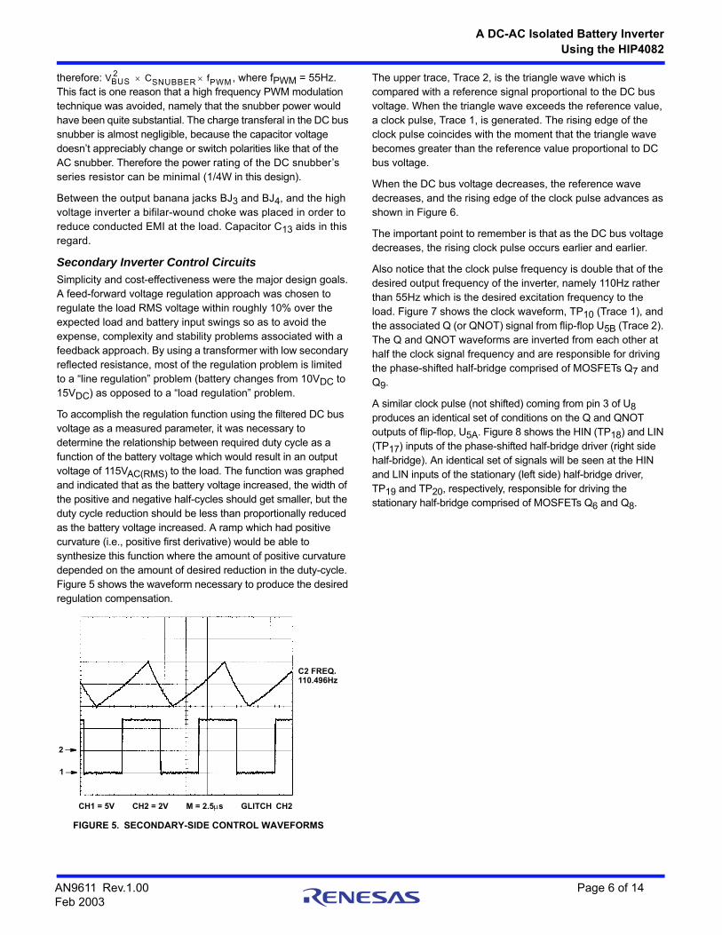
To accomplish the regulation function using the filtered DC bus voltage as a measured parameter, it was necessary to determine the relationship between required duty cycle as a function of the battery voltage which would result in an output voltage of 115VAC(RMS) to the load. The function was graphed and indicated that as the battery voltage increased, the width of the positive and negative half-cycles should get smaller, but the duty cycle reduction should be less than proportionally reduced as the battery voltage increased. A ramp which had positive curvature (i.e., positive first derivative) would be able to synthesize this function where the amount of positive curvature depended on the amount of desired reduction in the duty-cycle. Figure 5 shows the waveform necessary to produce the desired regulation compensation.
The upper trace, Trace 2, is the triangle wave which is compared with a reference signal proportional to the DC bus voltage. When the triangle wave exceeds the reference value, a clock pulse, Trace 1, is generated. The rising edge of the clock pulse coincides with the moment that the triangle wave becomes greater than the reference value proportional to DC bus voltage.
When the DC bus voltage decreases, the reference wave decreases, and the rising edge of the clock pulse advances as shown in Figure 6.
The important point to remember is that as the DC bus voltage decreases, the rising clock pulse occurs earlier and earlier.
Also notice that the clock pulse frequency is double that of the desired output frequency of the inverter, namely 110Hz rather than 55Hz which is the desired excitation frequency to the load. Figure 7 shows the clock waveform, TP10 (Trace 1), and the associated Q (or QNOT) signal from flip-flop U5B (Trace 2). The Q and QNOT waveforms are inverted from each other at half the clock signal frequency and are responsible for driving the phase-shifted half-bridge comprised of MOSFETs Q7 and Q9.
A similar clock pulse (not shifted) coming from pin 3 of U8 produces an identical set of conditions on the Q and QNOT outputs of flip-flop, U5A. Figure 8 shows the HIN (TP18) and LIN (TP17) inputs of the phase-shifted half-bridge driver (right side half-bridge). An identical set of signals will be seen at the HIN and LIN inputs of the stationary (left side) half-bridge driver, TP19 and TP20, respectively, responsible for driving the stationary half-bridge comprised of MOSFETs Q6 and Q8.
VBUS2 CSNUBBER fPWM
1
2
CH1 = 5V CH2 = 2V M = 2.5s GLITCH CH2
C2 FREQ.110.496Hz
FIGURE 5. SECONDARY-SIDE CONTROL WAVEFORMS
AN9611 Rev.1.00 Page 6 of 14Feb 2003

A DC-AC Isolated Battery Inverter
Using the HIP4082
The left and right half side half-bridges must be synchronized. The left half-bridge switching is perfectly synchronized with the minimum instances of the triangle wave and is therefore fixed in phase with the triangle wave. The right half-bridge slides with the level of the signal proportional to the DC bus voltage level as
previously mentioned. When the triangle wave reaches a minimum, a positive rising pulse is output at pin 3 of the ICM7555 timer, U8. This rising edge ‘clocks’ the U5A flip-flop which will either result in a high level at U5A’s Q or QNOT outputs, depending on the state of the data, D, input pin. It is not important which goes high first, only that the toggling of the Q and QNOT outputs of U5A alternate at each positive clock pulse from pin 3 of U8. The timer’s output, pin 3, goes low each time that the triangle wave reaches a peak.
Of paramount importance, however, is the need to synchronize the state of U5B’s Q and QNOT outputs with those of U5A. Arbitrarily the Q output of U5A was chosen to drive the upper left MOSFET in the left half-bridge (QNOT obviously drives the lower MOSFET). It is necessary that whenever the upper MOSFET of the left half-bridge is gated that the lower MOSFET in the right half-bridge also will be gated sometime within the same half-cycle. To guarantee that this happens it is necessary to connect either the Q or QNOT output of U5A to the data, D, input of U5B. If the Q output of U5A, which corresponds to the upper left MOSFET gate drive, is chosen to drive the D input of U5B, the next clock pulse from the phase-shifted clock which goes to U5B’s clock input pin must gate the lower right MOSFET, which corresponds to the LIN input of the right half-bridge driver, U9. Therefore the Q output signal of U5B must drive the LIN input of U9 and the QNOT signal of U5B must drive the HIN input of U9.
The waveforms in Figure 4 show the phase voltage waveforms of the left and right half-bridges and the resulting output voltage waveform shown in Figure 3. Notice that the algebraic difference between Trace 2 and Trace 1 waveforms precisely result in a waveform like that of Figure 3.
Unlike the HIP4082 and other members of the HIP408X family, the HIP2500 high voltage half-bridge driver requires external circuitry to insure that the upper and lower MOSFETs in a half-bridge leg do not conduct simultaneously. The quad AND-gate, U6, and resistors R24-R27, and capacitors C14-C17 tailor the dead-time to the needs of any application. Each Q and QNOT output from the flip-flops go directly to one input of a two input AND-gate and also through an R-C delay to the 2nd input of the AND-gate. Only after the R-C delay can the output of an AND-gate go high. Conversely, when any of the Q or QNOT outputs go low, a zero is placed on one of the AND-gate inputs and the AND-gate’s output immediately goes low. Therefore an ON-DELAY is produced, but no corresponding OFF-DELAY is produced.
Overcurrent Protection
An instantaneous overcurrent function senses the voltage drop across R23 for the purposes of shutting down the secondary-side inverter. The circuit comprising U7A, R28, R29, R32, R36, shunt resistor R23 and capacitor, C32 dictate the current trip level. The values shown in the schematic should cause overcurrent trip at approximately 1.3A. The voltage on the negative summing junction of U7A dictates the trip level based upon the divider action of R29 and R32. The output of U7A
1
2
CH1 = 5V CH2 = 2V M = 2.5s GLITCH CH2
C2 FREQ.110.04Hz
FIGURE 6. SECONDARY-SIDE CONTROL WAVEFORMS WITH LOWER DC BUS VOLTAGE
1
2
CH1 = 5V CH2 = 5V M = 2.5s GLITCH CH2
C2 FREQ.55.552Hz
FIGURE 7. SECONDARY-SIDE FLIP-FLOP WAVEFORMS
1
2
CH1 = 5V CH2 = 5V M = 2.5s GLITCH CH2
C2 FREQ.55.872Hz
FIGURE 8. HIP2500 INPUT WAVEFORMS
AN9611 Rev.1.00 Page 7 of 14Feb 2003
A DC-AC Isolated Battery Inverter
Using the HIP4082
goes to the SD input of both HIP2500 high voltage half-bridge drivers, disabling them.
Once tripping has occurred, reset must be accomplished by removing input voltage to the eval-board, as R28 provides enough hysteresis such that even after the load current is dropped to zero (no signal at the SHUNT resistor), the voltage on the positive summing junction of U7A will exceed that on the negative summing junction.
Overtemperature Protection
Resistors R10 - R12, R14, RT1 and diode D4, provide the overtemperature function. Overtemperature does not shut down the eval-board as in the case of overcurrent. Instead, the duty-cycle of the output voltage waveform is reduced, thereby reducing the RMS output voltage. This is accomplished by faking the voltage control function into thinking that the input voltage is higher than it really is.
When the thermistor, RT1, temperature increases, its resistance decreases and the negative summing junction voltage on pin 6 of U4B decreases. Eventually, when it falls below the voltage on the positive summing junction, the output, pin 7, of U4B rises. The voltage on the positive summing junction is determined by the bias voltage and the ratio of R11 to R12. The temperature at which this happens is determined by the negative resistance characteristics of the thermistor chosen and its temperature. RT1 is attached by epoxy cement to one of the primary-side MOSFETs. Diode D4, blocks the voltage on the output pin 7 of U4B from affecting the inverter output voltage until after the overtemperature condition has been reached.
Snubbers
A DC bus voltage snubber has been employed to control or reduce transients across the bridge which might lead to breakdown failure in either the MOSFETs or the HIP2500 drivers, or both. The bus voltage transients are snubbed by the bus snubber comprised of resistor, R34 and capacitor, C23. A good reference on snubber design is found in Reference 2.
ConclusionA simple, cost-effective solution to designing low to medium voltage DC-to-AC inverters using the HIP4082 H-Bridge Gate Driver has been shown using the HIP4082 DC/AC Evaluation PC Board as a demonstration vehicle. Other approaches using the same HIP4082 can certainly be imagined and implemented with success.
Hopefully this application note will assist the designer in getting started on his or her own design. This same HIP4082 IC can also be used in AC-to-DC converters, such as those used in various motor controls and other high performance DC voltage controllers.
WARNINGA neon lamp was placed across the output of the inverter in order to warn users of the presence of HIGH VOLTAGE AND POTENTIAL SHOCK HAZARD.
AN9611 Rev.1.00 Page 8 of 14Feb 2003

A DC-AC Isolated Battery Inverter
Using the HIP4082
Schematic Diagram (1 of 3)
R2
R1
4.6
4K
0.0
01
F
TR
CT
L
RG
ND
TH
R
DIS
OU
TV
CC
U1
ICM
755
5
DS
Q
CL
K RQ
1.5
KT
P5
TP
4
10
R3
R8
C3
DS
Q
CL
K R
U2
10
D2
C2
C1
1.5F
D1
220
0F
16
VD
C
Q1
U11
B
CA
40
13B
E
CA
40
13B
E
220
0F
16
VD
C
F1
3A
G,
30A
32V
DC
C5
+C
6
R37
+B
AT
T
R5
Q4
R4
10
Q2
TP
2
C22
+B
AT
T
TP
3
0.2
2F
10
HIP
408
2
VS
S
DIS
DE
LA
HS
AL
O
BL
O
BH
S
AH
O
BH
O
AH
BB
HB
VD
D
AL
I
BH
I
AH
I
BL
I
10
0V
1
1/2
W
UF
400
2
TP
1
R7
1
1W
10% D3
15
V1
N5
929
B1.
5W
C4
22F
25V
DC
AC
1
AC
2
AC
3
AC
6
AC
5
AC
4
115
/23
0VA
C
TR
03
_03
Q3
VC
C
T1
VC
C
U11
A
VC
CB
J1
BJ
2
0.2
2F
+
XX
+
C7
6.8F
Q
OU
TP
UT
S
12
19
16
10
15
14
13
11
6
583724
1
2 3
12 3
12 3
1
2 3
61
0
935
8724
1112
1
813 12
10
11
9
65 3
1 2
67
4
3
8
2 5
1
4
NO
TE
S:
1.A
ll R
esis
tors
are
1%
, 1/8
W, u
nle
ss o
ther
wis
e sp
ecifi
ed.
2.A
ll R
esis
tor
valu
es a
re in
ohm
s, u
nles
s ot
herw
ise
spec
ified
.
3.A
ll po
lari
zed
capa
cito
rs a
re A
lum
. Ele
ctro
lytic
, +50
%, -
10%
, un
less
oth
erw
ise
spec
ified
.
4.A
ll ce
ram
ic c
apac
itors
are
50V
, 20%
unl
ess
othe
rwis
e sp
ecifi
ed.
5.Q
1, Q
2, Q
3, Q
4 a
re In
ters
il R
FP
70N
06.
6.C
onne
ct A
C3 to
AC
5 an
d A
C4 to
AC
6 fo
r 11
5VA
C.
7.F
or 2
30V
AC
out
, co
ntac
t Int
ersi
l.
XX
AN9611 Rev.1.00 Page 9 of 14Feb 2003

A DC-AC Isolated Battery Inverter
Using the HIP4082
Schematic Diagram (2 of 3)
VS
S
+-
+-A
C1
AC
2
D9
UF
400
2
HIG
H V
OLT
AG
E B
US
D5
D1
0
C9
D12
4.7F
50
VD
C
C11
0.1F
U3
1
UF
40
02
UF
40
02
1
1/2
W
TP
14
LM
78M
12
CP
INO
UT
GN
D
R34
C23
1/4
W0
.1F
20
0/4
00V
DC
C8
22
0F
TP
7
0.0
01
F
C30
Q6
IRF
63
6
R21
1.5
20
0/4
00V
DC
UF
54
050
.00
1F
IRF
63
6
TP
8
TP
15
R2
3
0.5
2W 5%
R22
15R
201
51
5
Q8
C29
TP
16
R19
0.00
1F
R18
15
TP
13
0.00
1F
Q9
IRF
636
C1
24
.7F T
P11
TR
IWA
VE
R16
12.1
K
Q7
IRF
63
6
L1
CH
OK
E
R15 1.5C
31
AC
3
AC
4
SH
UN
T
GT
L
VS
L
GB
L
GT
R
VS
R
GB
R
C1
30
.1F
20
0/4
00V
DC
LP
1L
AM
P
115V
AC
55
Hz
OU
T
R33
82
.5K
BJ
3
TP
10
CL
OC
K
U4A C
A3
260
+1
2V
BJ
4
+12
V
C1
0
0.1F
R13
10
K
RE
SE
TR
111
0K
RT
11
0K
AT
25
oC
toR
1720
K
D4
1N41
48
U4B
CA
326
0
R14
200
K
OV
ER
TE
MP
LIM
ITT
P9
SE
CO
ND
AR
Y S
IDE
BIA
S
R1
22
.21
K
R10
10
K
TP
12
+1
2V
TP
6
R35
D11
UF
400
2
R9
332
K1
/4W
C26
2.2F
50
V
D6
UF
540
5
D7
UF
540
5D
8U
F5
40
5
12
34
3 2
4
1
8
1
11
222
333
1
2 3
1
2
3
6 57
1 2
C28
AN9611 Rev.1.00 Page 10 of 14Feb 2003

A DC-AC Isolated Battery Inverter
Using the HIP4082
Schematic Diagram (3 of 3)
Q Q
CL
K
DS R
Q12
CU
RR
EN
T L
IMIT
Q10
Q11
R32
+1
2V
2N3
90
62
N3
906
+1
2V
100
KC
321
.0F
10
0K
2N39
04
R36
P1
D13
R31
681
K0 +
12
VR
30
12
.1K
TR
IWA
VE
+12
V
10
K
+ -C
A3
260
4.6
4K
R2
9
U5
A
R28
TP
22
38.
3K
U7A
CL
R2
4
DE
AD
-TIM
E
0.1FC14
R2
6
TP
19C
A32
60
U7
B
+-
TP
20 U6A
Q Q
CL
K
DS R
4.7
CA
40
13B
E
U5B
OU
T
TH
R
CT
L
TR
VC
C
GN
D
DIS
R
X
U8
ICM
75
55C
180.
22
F
4.7
4.7
4.7
R2
5
R2
7
0.1F
0.1F
0.1FC16
C15
C17
CA
40
13B
E
CL
OC
K
RE
SE
T
TR
IWA
VE
+1
2V
VD
D
TP
18T
P17
CA
408
1B
E
CA
408
1B
E
CA
408
1B
E
CA
408
1B
E
U6D
U6B
U6C
C25
1.5F
VD
DV
CC
VB
HIN H
IP2
500
IP
SD
LIN V
SS
CO
M
LO
VS
HO
UF
40
05
VD
D
VC
CV
B
HIN
D14
HIP
25
00IP
SD
LIN
VS
SC
OMLOVS
HO
GB
L
50V
DC
50
VD
C
VS
L
GT
L
1.5F
50
VD
C
C19
C20
VS
S
1.5F
1.5F
50V
DC
+1
2V
500
V
GT
R
VS
R
GB
R
500
VU
10
UF
400
5D
17
UF
400
5
UF
400
5D
16+
12V
+1
2V
C24
D15
+12
VU
9
SH
UN
T
1 2
4
356 8
13
12
10
11
9
5 64
13
12
11
213
4
231
8
6 57
28
3 7 6
1
45
36
7 5 1
21
3
12
11109
36
7 5 1
21
3
12
11109
12
3 12
3
981
0
AN9611 Rev.1.00 Page 11 of 14Feb 2003
A DC-AC Isolated Battery Inverter
Using the HIP4082
References[1] Danz, George E., “HIP4082” data sheet, Intersil Corp. Mel-
bourne, FL, 1994, File Number 3676.
[2] Pressman, Abraham I., "Switching Power Supply Design," McGraw Hill, 1991, Chapt. 11.
AppendixParts List
ITEM QUANTITY REFERENCE PART DESCRIPTION VENDOR/NO.
1 4 BJ1, BJ2, BJ3, BJ4 Banana Jack
2 3 C1, C2, C18 0.22F, 50V Ceramic
3 5 C3, C28, C29, C30, C31 0.001F, 50V Ceramic
4 1 C4 22F, 25V Electrolytic
5 2 C6, C5 2200F, 16V Electrolytic
6 1 C7 6.8F, 50V Ceramic
7 1 C8 220F, 250V Electrolytic
8 2 C9, C12 4.7F, 50V Ceramic
9 6 C10, C11, C14, C15, C16, C17 0.1F, 50V Ceramic
10 2 C13, C23 0.1F, 200V Ceramic
11 5 C19, C20, C22, C24, C25 1.5F, 50V Ceramic
12 1 C26 2.2F, 50V Ceramic
13 1 C32 1.0F, 50V Ceramic
14 6 D1, D2, D9, D10, D11, D12 UF4002 General Instruments
15 1 D3 1N5929B General Instruments
16 1 D4 1N4148 General Instruments
17 4 D5, D6, D7, D8 UF5405 General Instruments
18 1 D13 0Jumper
19 4 D14, D15, D16, D17 UF4005 General Inst.
20 1 F1 3AG,30A 32VDC Bussman
21 1 LP1 Lamp Sylvania, NE2/A1A, Code 323650
22 1 L1 Choke TNI, type T7192
23 1 P1 100K 10T Mini Trim Pot
24 4 Q1, Q2, Q3, Q4 RFP70N06 Intersil
25 4 Q6, Q7, Q8, Q9 IRF731 Intersil
26 1 Q10 2N3904
27 2 Q11, Q12 2N3906
28 1 RT1 Thermistor 10K at 25oC Keystone, AL03006-581897-G1
29 2 R1, R29 4.64K 1% 1/4W
30 1 R2 15.0K 1% 1/4W
31 4 R3, R4, R5, R8 10 1% 1/4W
32 1 R7 1 1% 1W
33 1 R34 1 1% 1/4W
34 1 R9 332K 1% 1/4W
35 4 R10, R11, R13, R36 10.0K 1% 1/4W
36 1 R12 2.21K 1% 1/4W
AN9611 Rev.1.00 Page 12 of 14Feb 2003

A DC-AC Isolated Battery Inverter
Using the HIP4082
37 1 R32 100K 1% 1/4W
38 1 R14 200K 1% 1/4W
39 1 R17 20.0K 1% 1/4W
40 2 R15, R21 1.5 1% 1/4W
41 1 R16, R30 12.1K 1% 1/4W
42 4 R18, R19, R20, R22 15 1% 1/4W
43 1 R23 0.5 1% 2W
44 4 R24, R25, R26, R27 4.7 5% 1/4W
45 1 R28 38.3K 1% 1/4W
46 1 R31 681K 1% 1/4W
47 1 R33 82.5K 1% 1/4W
48 2 R35, R37 1 5% 1/2W
49 21 TP1 - TP20, TP22 Test Point Berg, (BergStik)
50 1 T1 Transformer TNI, type T6905
51 2 U1, U8 ICM7555
52 1 U2 HIP4082IP
53 1 U3 MC78M12CT Motorola
54 2 U4, U7 CA3260AE Intersil
55 2 U5, U11 CD4013BE Intersil
56 1 U6 CD4081BE Intersil
57 2 U9, U10 HIP2500IP Intersil
58 4 HS1-4 576802B00000, Heat Sink AAVID
Parts List (Continued)
ITEM QUANTITY REFERENCE PART DESCRIPTION VENDOR/NO.
AN9611 Rev.1.00 Page 13 of 14Feb 2003

http://www.renesas.comRefer to "http://www.renesas.com/" for the latest and detailed information.
Renesas Electronics America Inc.1001 Murphy Ranch Road, Milpitas, CA 95035, U.S.A.Tel: +1-408-432-8888, Fax: +1-408-434-5351Renesas Electronics Canada Limited9251 Yonge Street, Suite 8309 Richmond Hill, Ontario Canada L4C 9T3Tel: +1-905-237-2004Renesas Electronics Europe LimitedDukes Meadow, Millboard Road, Bourne End, Buckinghamshire, SL8 5FH, U.KTel: +44-1628-651-700, Fax: +44-1628-651-804Renesas Electronics Europe GmbHArcadiastrasse 10, 40472 Düsseldorf, Germany Tel: +49-211-6503-0, Fax: +49-211-6503-1327Renesas Electronics (China) Co., Ltd.Room 1709 Quantum Plaza, No.27 ZhichunLu, Haidian District, Beijing, 100191 P. R. ChinaTel: +86-10-8235-1155, Fax: +86-10-8235-7679Renesas Electronics (Shanghai) Co., Ltd.Unit 301, Tower A, Central Towers, 555 Langao Road, Putuo District, Shanghai, 200333 P. R. China Tel: +86-21-2226-0888, Fax: +86-21-2226-0999Renesas Electronics Hong Kong LimitedUnit 1601-1611, 16/F., Tower 2, Grand Century Place, 193 Prince Edward Road West, Mongkok, Kowloon, Hong KongTel: +852-2265-6688, Fax: +852 2886-9022Renesas Electronics Taiwan Co., Ltd.13F, No. 363, Fu Shing North Road, Taipei 10543, TaiwanTel: +886-2-8175-9600, Fax: +886 2-8175-9670Renesas Electronics Singapore Pte. Ltd.80 Bendemeer Road, Unit #06-02 Hyflux Innovation Centre, Singapore 339949Tel: +65-6213-0200, Fax: +65-6213-0300Renesas Electronics Malaysia Sdn.Bhd.Unit 1207, Block B, Menara Amcorp, Amcorp Trade Centre, No. 18, Jln Persiaran Barat, 46050 Petaling Jaya, Selangor Darul Ehsan, MalaysiaTel: +60-3-7955-9390, Fax: +60-3-7955-9510Renesas Electronics India Pvt. Ltd.No.777C, 100 Feet Road, HAL 2nd Stage, Indiranagar, Bangalore 560 038, IndiaTel: +91-80-67208700, Fax: +91-80-67208777Renesas Electronics Korea Co., Ltd.17F, KAMCO Yangjae Tower, 262, Gangnam-daero, Gangnam-gu, Seoul, 06265 KoreaTel: +82-2-558-3737, Fax: +82-2-558-5338
SALES OFFICES
© 2018 Renesas Electronics Corporation. All rights reserved.Colophon 7.0
(Rev.4.0-1 November 2017)
Notice
1. Descriptions of circuits, software and other related information in this document are provided only to illustrate the operation of semiconductor products and application examples. You are fully responsible for
the incorporation or any other use of the circuits, software, and information in the design of your product or system. Renesas Electronics disclaims any and all liability for any losses and damages incurred by
you or third parties arising from the use of these circuits, software, or information.
2. Renesas Electronics hereby expressly disclaims any warranties against and liability for infringement or any other claims involving patents, copyrights, or other intellectual property rights of third parties, by or
arising from the use of Renesas Electronics products or technical information described in this document, including but not limited to, the product data, drawings, charts, programs, algorithms, and application
examples.
3. No license, express, implied or otherwise, is granted hereby under any patents, copyrights or other intellectual property rights of Renesas Electronics or others.
4. You shall not alter, modify, copy, or reverse engineer any Renesas Electronics product, whether in whole or in part. Renesas Electronics disclaims any and all liability for any losses or damages incurred by
you or third parties arising from such alteration, modification, copying or reverse engineering.
5. Renesas Electronics products are classified according to the following two quality grades: “Standard” and “High Quality”. The intended applications for each Renesas Electronics product depends on the
product’s quality grade, as indicated below.
"Standard": Computers; office equipment; communications equipment; test and measurement equipment; audio and visual equipment; home electronic appliances; machine tools; personal electronic
equipment; industrial robots; etc.
"High Quality": Transportation equipment (automobiles, trains, ships, etc.); traffic control (traffic lights); large-scale communication equipment; key financial terminal systems; safety control equipment; etc.
Unless expressly designated as a high reliability product or a product for harsh environments in a Renesas Electronics data sheet or other Renesas Electronics document, Renesas Electronics products are
not intended or authorized for use in products or systems that may pose a direct threat to human life or bodily injury (artificial life support devices or systems; surgical implantations; etc.), or may cause
serious property damage (space system; undersea repeaters; nuclear power control systems; aircraft control systems; key plant systems; military equipment; etc.). Renesas Electronics disclaims any and all
liability for any damages or losses incurred by you or any third parties arising from the use of any Renesas Electronics product that is inconsistent with any Renesas Electronics data sheet, user’s manual or
other Renesas Electronics document.
6. When using Renesas Electronics products, refer to the latest product information (data sheets, user’s manuals, application notes, “General Notes for Handling and Using Semiconductor Devices” in the
reliability handbook, etc.), and ensure that usage conditions are within the ranges specified by Renesas Electronics with respect to maximum ratings, operating power supply voltage range, heat dissipation
characteristics, installation, etc. Renesas Electronics disclaims any and all liability for any malfunctions, failure or accident arising out of the use of Renesas Electronics products outside of such specified
ranges.
7. Although Renesas Electronics endeavors to improve the quality and reliability of Renesas Electronics products, semiconductor products have specific characteristics, such as the occurrence of failure at a
certain rate and malfunctions under certain use conditions. Unless designated as a high reliability product or a product for harsh environments in a Renesas Electronics data sheet or other Renesas
Electronics document, Renesas Electronics products are not subject to radiation resistance design. You are responsible for implementing safety measures to guard against the possibility of bodily injury, injury
or damage caused by fire, and/or danger to the public in the event of a failure or malfunction of Renesas Electronics products, such as safety design for hardware and software, including but not limited to
redundancy, fire control and malfunction prevention, appropriate treatment for aging degradation or any other appropriate measures. Because the evaluation of microcomputer software alone is very difficult
and impractical, you are responsible for evaluating the safety of the final products or systems manufactured by you.
8. Please contact a Renesas Electronics sales office for details as to environmental matters such as the environmental compatibility of each Renesas Electronics product. You are responsible for carefully and
sufficiently investigating applicable laws and regulations that regulate the inclusion or use of controlled substances, including without limitation, the EU RoHS Directive, and using Renesas Electronics
products in compliance with all these applicable laws and regulations. Renesas Electronics disclaims any and all liability for damages or losses occurring as a result of your noncompliance with applicable
laws and regulations.
9. Renesas Electronics products and technologies shall not be used for or incorporated into any products or systems whose manufacture, use, or sale is prohibited under any applicable domestic or foreign laws
or regulations. You shall comply with any applicable export control laws and regulations promulgated and administered by the governments of any countries asserting jurisdiction over the parties or
transactions.
10. It is the responsibility of the buyer or distributor of Renesas Electronics products, or any other party who distributes, disposes of, or otherwise sells or transfers the product to a third party, to notify such third
party in advance of the contents and conditions set forth in this document.
11. This document shall not be reprinted, reproduced or duplicated in any form, in whole or in part, without prior written consent of Renesas Electronics.
12. Please contact a Renesas Electronics sales office if you have any questions regarding the information contained in this document or Renesas Electronics products.
(Note 1) “Renesas Electronics” as used in this document means Renesas Electronics Corporation and also includes its directly or indirectly controlled subsidiaries.
(Note 2) “Renesas Electronics product(s)” means any product developed or manufactured by or for Renesas Electronics.