an41908a - panasonic · 44 43 42 41 40 39 38 37 36 35 34 ... an41908a 5 ver. beb 3.02 1.02 0 input...
TRANSCRIPT

AN41908A
1 Ver. BEB
・ Voltage drive system 256-step microstep drivers(2 systems)(Super low noise Zoom and Focus drive)
・ Built-in Iris controller・ Motor control by 4-line serial data communication・ 2 systems of open-drain for driving LED・ PCB space saving. ・ Low power consumption of Iris drive by PWM・ 44 pin Plastic Quad Flat Non-leaded Package
(QFN Type)
・Camcorder, Security-camera
SIMPLIFIED APPLICATION
APPLICATIONS
FEATURES DESCRIPTION
Lens Driver IC for camcorder and security-camera incorporating Iris control
AN41908A is a lens motor driver IC for camcorder and security-camera featuring the functions of Iris control. Voltage drive system and several torque ripple correction techniques enable super- low noise microstep drive.
Notes)This application circuit is an example. The operation of massproduction set is not guaranteed. You should perform enoughevaluation and verification on the design of mass production set.You are fully responsible for the incorporation of the aboveapplication circuit and information in the design of your equipment.
V+
V–
1
2
3
4
5
6
7
8
9
10
11
OP3INP
SENS
OP3OUT
REF
AVDD3
ADTESTIN
TEST
OUTE2
VDD5
GND5
OUTE1
12 13 14 15 16 17 18 19 20 21 22
N.C
.
OU
TD2
OU
TD1
MG
ND
B
OU
TC2
OU
TC1
MV
CC
B
OU
TB2
OU
TB1
OU
TA2
MV
CC
A
44 43 42 41 40 39 38 37 36 35 34
PLS
1
SINVD
_FZ
VD
_IS
RS
TB
OP
4OU
T
OP
4IN
N
VR
EF
GN
DA
CR
EFI
N
PLS
2
23
33
32
31
30
29
28
27
26
25
24MGNDAOUTA1
N.C.
SCK
SOUT
CS
GNDD
LED2
LED1
OSCIN
DVDD
HallSensorH–
H+
0.1
μF
100
pF
0.1
μF
10 kΩAVDD3(3.1 V)
M
VDD5(4.8 V)
MVCCB(4.8 V)
MVCCA(4.8 V)
DVDD(3.1 V)
0.01 μF
Noi
se L
evel
(dB
)
No Correction
With Correction
-15
-10
-5
0
5
10
15
20
25
30
35
2.50Hz
32.50Hz
62.50Hz
92.50Hz
122.50Hz
152.50Hz
182.50Hz
212.50Hz
242.50Hz
272.50Hz
302.50Hz
332.50Hz
362.50Hz
392.50Hz
422.50Hz
452.50Hz
482.50Hz
512.50Hz
542.50Hz
572.50Hz
602.50Hz
632.50Hz
662.50Hz
692.50Hz
722.50Hz
752.50Hz
782.50Hz
812.50Hz
842.50Hz
872.50Hz
902.50Hz
932.50Hz
962.50Hz
992.50Hz
Frequency (Hz)
Frequency (Hz)
Noi
se L
evel
(dB
)
Super low noise Zoom and Focus drive.
–10 dB
Publication date: November 2012

AN41908A
2 Ver. BEB
ABSOLUTE MAXIMUM RATINGS
*3V–0.3 to (DVDD + 0.3)PLS1, PLS2, SOUT
*3V–0.3 to (AVDD3 + 0.3)OP3OUT, OP4OUT,
SENS,VREFOutput Voltage Range
—mA30LED1, LED2Output Current Range
*2°C–20 to + 125TjOperating junction temperature
–0.3 to + 4.0DVDD
*1V–0.3 to + 6.0VDD5Supply voltage for motor controller 2
*1V–0.3 to + 6.0MVCCA, MVCCBSupply voltage for motor controller 1
*1V–0.3 to + 4.0AVDD3
Controller supply voltage
*3V–0.3 to (DVDD + 0.3)TEST, OSCIN,CS, SCK, SIN,
VD_IS, VD_FZ, RSTB
*2°C–55 to + 125TstgStorage temperature
—A/ch±0.25
OUTA1, OUTA2,OUTB1, OUTB2,OUTC1, OUTC2,OUTD1, OUTD2
Motor driver 1 (focus, zoom)H bridge drive current (DC current)
*2, *4°C–20 to + 85ToprOperating ambient temperature
—A/ch±0.4IM(pulse)Instantaneous H bridge drive current
*3V–0.3 to (AVDD3 + 0.3)OP3INP, OP4INN,
ADTESTIN,REF, CREFIN
Input Voltage Range
—kV±2HBM (Human Body Model)ESD
—kV±1CDM (Charge Device Model)
NoteUnitRatingSymbolParameter
—A/ch±0.15OUTE1, OUTE2Motor driver 2 (iris)H bridge drive current(DC current)
Notes). This product may sustain permanent damage if subjected to conditions higher than the above stated absolute maximum rating. This rating is the maximum rating and device operating at this range is not guaranteeable as it is higher than our stated recommended operating range.When subjected under the absolute maximum rating for a long time, the reliability of the product may be affected.*1:The values under the condition not exceeding the above absolute maximum ratings and the power dissipation.*2:Except for the power dissipation, operating ambient temperature, and storage temperature, all ratings are for Ta = 25°C.*3: (DVDD + 0.3 ) V must not be exceeded 4.0 V and (AVDD + 0.3 ) V must not be exceeded 4.0 V.*4:The power dissipation shown is the value at Ta = 85°C for the independent (unmounted) IC package without a heat sink.
When using this IC, refer to the PD-Ta diagram of the package standard and design the heat radiation with sufficient margin so that the allowable value might not be exceeded based on the conditions of power supply voltage, load, andambient temperature.

AN41908A
3 Ver. BEB
RECOMMENDED OPERATING CONDITIONS
*2VDVDD + 0.3-–0.3PLS1, PLS2, SOUT
*2VAVDD3 + 0.3-–0.3
OP3OUT, OP4OUT,SENS,VREF
Output Voltage Range
*1mA30--LED1, LED2
*1A0.15--0.15OUTE1, OUTE2
*1A0.25--0.25
OUTA1, OUTA2,OUTB1, OUTB2,OUTC1, OUTC2,OUTD1, OUTD2Output Current Range
—μF0.01COP3INP
*1V3.63.12.7AVDD3,DVDD
*2VDVDD + 0.3-–0.3
TEST, OSCIN,CS, SCK, SIN,VD_IS, VD_FZ,
RSTB
—kΩ10RREF
—μF0.1CREFIN
—pF100CVREF
—μF0.1COP4OUT
External Constants
-
4.8
Typ.
—°C85-20TaoprOperating ambient temperature
*2VAVDD3 + 0.3–0.3
OP3INP, OP4INN,ADTESTIN,
REF, CREFINInput Voltage Range
3.0
Min.
*1V5.5MVCCA, MVCCB, VDD5
Supply voltage range
NoteUnitMax.SymbolParameter
CAUTIONAlthough this has limited built-in ESD protection circuit, but permanent damage may occur on it.Therefore, proper ESD precautions are recommended to avoid electrostatic damage to the MOS gates
0.765W1.392W71.8℃/WMount on PWB *1
0.194W0.353W282.9℃/WWithout PWB
PD (Ta=70 °C)PD (Ta=25 °C)θ JACondition
POWER DISSIPATION RATING
Note). For the actual usage, please refer to the PD-Ta characteristics diagram in the package specification, supply voltage, load and ambient temperature conditions to ensure that there is enough margin follow the power and the thermal design does not exceed the allowable value.
*1: Glass-Epoxy: 50×50×0.8 (mm) , heat dissipation fin: Dai-pad , the state where it does not mount.
Note) *1 : The values under the condition not exceeding the above absolute maximum ratings and the power dissipation.*2 : (DVDD + 0.3 ) V must not be exceeded 4.0 V and (AVDD + 0.3 ) V must not be exceeded 4.0 V.

AN41908A
4 Ver. BEB
μA
Ω
μA
Ω
μA
Ω
—
IM = 100 mA
0.8———IleakIRH bridge leak current
LED driver
8——I = 20 mA, 5 V cellRonLEDOutput ON resistance
mA10.05.0—RSTB = High, output open, 27 MHz input,Total current
IccstandbySupply current on Standby
mA12.06.0—
RSTB = High, output open,27 MHz input, FZ = Enable,Total current
IccpsSupply current when FZ is Enable and Iris is in power save mode
mA1.00.3—Output openIcc5enableVDD5 supply current on Enable
V0.2 ×DVDD—–0.3RSTBVin(L)Low-level input
V——DVDD– 0.5
[SOUT] 1 mA SourceVout(H) : SDATASOUT High-level output
V0.5——[SOUT] 1 mA SinkVout(L) : SDATA
SOUT Low-level output
V——0.9 ×
DVDD—Vout(H) : MUX
PLS1 to 2High-level output
V0.1 ×DVDD———Vout(L) : MUX
PLS1 to 2Low-level output
kΩ20010050RSTBRpullretInput pull-down resistance
Motor driver 1 (focus, zoom)
2.5——RonFZH bridge ON resistance
0.8——IleakFZH bridge leak current
Motor driver 2 (iris)5——IM = 50 mARonIRH bridge ON resistance
0.8———IleakLEDOutput leak current
mA150.5—Output openImenableMVCC supply current on Enable
μA10.00—No 27 MHz inputIcc3reset3 V supply current on Reset
mA20.07.0—Output openIcc3enable3 V supply current on Enable
μA3.00—No 27 MHz inputIcc5resetVDD5 supply current on Reset
VDVDD+ 0.3—
0.54 ×DVDD
RSTBVin(H)High-level input
Digital input / output
Current circuit, Common circuit
μA3.00—No load, no 27 MHz inputIOmdisableMVCC supply current on Reset
LimitsTyp
UnitMax
NoteMin
Condition SymbolParameter
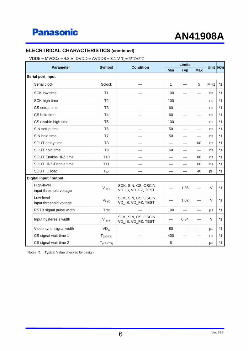
ELECRTRICAL CHARACTERISTICSVDD5 = MVCCx = 4.8 V, DVDD = AVDD3 = 3.1 V Ta = 25°C±2°C

AN41908A
5 Ver. BEB
3.02
1.02
0
mV10—–10—VOFInput offset voltage
V½
AVDD3 + 0.1
—½
AVDD3– 0.1
—VINInput voltage range
V0.20.1—ILOAD = –10 μAVOLOutput voltage (Low)
V—AVDD3– 0.2
AVDD3– 0.5
ILOAD = 3 mAVOHOutput voltage (High)
OPAMP4 (HALL Sensor Amp. for eliminating common-mode voltage)
VVREF+ 0.1
VREFVREF– 0.1
ILOAD = ±100 μA, CVREF = 100 pF
VREFLOutput voltage 2
Hall bias controller (SENS pin output)
mA0.1—REF = 10 kΩ,SENS = 0.7 VSetting value : 00 h
IBLMin. output current
mA1.140.9REF = 10 kΩ,SENS = 0.7 VSetting value : 40 h
IB40HOutput current accuracy 1
mA3.382.66REF = 10 kΩ,SENS = 0.7 VSetting value : BE h
IBBFHOutput current accuracy 2
mV15—–15—VOFInput offset voltage
V0.20.1—ILOAD = –100 μAVOLOutput voltage (Low)
V—AVDD3– 0.1
AVDD3– 0.2
ILOAD = 100 μAVOHOutput voltage (High)
V/V24.121.919.7Gain setting value : 0hVOGGain
V½
AVDD3 + 0.1
½AVDD3
½AVDD3– 0.1
ILOAD = 0 A, CVREF = 100 pF
VREFOutput voltage 1
Reference voltage output block
OPAMP3 (HALL Sensor Amp. for output amplifier)
V½
AVDD3 + 0.5
½AVDD3
½AVDD3– 0.5
—VINInput voltage range
LimitsTyp
UnitMax
NoteMin
Condition SymbolParameter
ELECRTRICAL CHARACTERISTICS (continued)
VDD5 = MVCCx = 4.8 V, DVDD = AVDD3 = 3.1 V Ta = 25°C±2°C
AN41908A
6 Ver. BEB
*1MHz5—1—SclockSerial clock
*1ns60———T8SOUT delay time
*1ns——60—T9SOUT hold time
*1ns60———T10SOUT Enable-Hi-Z time
*1ns60———T11SOUT Hi-Z-Enable time
*1pF40———TSCSOUT C load
Digital input / output
*1V—1.36—SCK, SIN, CS, OSCIN, VD_IS, VD_FZ, TESTVin(H)
High-levelinput threshold voltage
*1V—1.02—SCK, SIN, CS, OSCIN, VD_IS, VD_FZ, TESTVin(L)
Low-levelinput threshold voltage
*1μs——100—TrstRSTB signal pulse width
*1V—0.34—SCK, SIN, CS, OSCIN, VD_IS, VD_FZ, TESTVhysinInput hysteresis width
*1μs——80—VDWVideo sync. signal width
*1ns——400—T(VD-CS)CS signal wait time 1
*1μs——5—T(CS-DT1)CS signal wait time 2
*1ns——100—T2SCK high time
*1ns——60—T3CS setup time
*1ns——60—T4CS hold time
*1ns——100—T5CS disable high time
*1ns——50—T7SIN hold time
Serial port input
*1ns——50—T6SIN setup time
*1ns——100—T1SCK low time
LimitsTyp
UnitMax
NoteMin
Condition SymbolParameter
ELECRTRICAL CHARACTERISTICS (continued)
VDD5 = MVCCx = 4.8 V, DVDD = AVDD3 = 3.1 V Ta = 25°C±2°C
Note) *1 :Typical Value checked by design.

AN41908A
7 Ver. BEB
10 bit ADC
*1V—0——DAOTLofAdjustment range (Low)
*1V—AVDD3——DAOTHofAdjustment range (High)
*1μs—1.2—OSCIN = 27 MHzPL1widthPulse resolution for pulse 1
*1°C—40——Δ TtsdThermal shutdown hysteresis width
*1°C—150——TtsdThermal shutdown operation temperature
*1V—2.27——Vrston3.3 V Reset operation
Supply voltage monitor circuit
*1V—2.2——VrstFZonMVCCx Reset operation
*1V—0.2——Vrsthys3.3 V Reset hysteresis width
*1V—2.2——VrstISonVDD5 Reset operation
*1V—0.2——VrstFZhysMVCCx Reset hysteresis width
8 bit DAC for Hall Offset adjustment
*1V—0.2——VrstIShysVDD5 Reset hysteresis width
*1V——0.2—Vin(L)Input Range (Low)
*1VAVDD3 – 0.2———Vin(H)Input Range (High)
*1LSB—2.0——INL10AINLE (Integral linearity error)
*1LSB—1.0——DNL10ADNLE(Differential linearity error)
*1μs—20.1—OSCIN = 27 MHzPL2waitPulse start resolution for pulse 2
Iris control
*1kHz—500—OSCIN = 27 MHzIRISSampleAD sampling frequency
Iris control
Pulse generator
*1μs—20.1—OSCIN = 27 MHzPL1waitPulse start resolution for pulse 1
LimitsTyp
UnitMax
NoteMin
Condition SymbolParameter
ELECRTRICAL CHARACTERISTICS (continued)
VDD5 = MVCCx = 4.8 V, DVDD = AVDD3 = 3.1 V Ta = 25°C±2°C
Note) *1 :Typical Value checked by design.
AN41908A
8 Ver. BEB
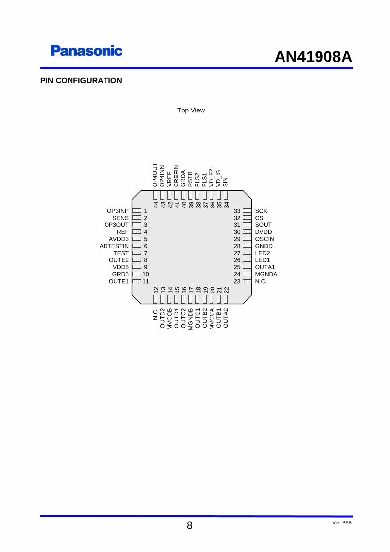
PIN CONFIGURATION
Top View
1234567891011
OP3INPSENS
OP3OUTREF
AVDD3ADTESTIN
TESTOUTE2
VDD5GRD5
OUTE1
3332313029282726252423
44 43 42 41 40 39 38 37 36 35 34
12 13 14 15 16 17 18 19 20 21 22
SCKCSSOUTDVDDOSCINGNDDLED2LED1OUTA1MGNDAN.C.
OP
4OU
TO
P4I
NN
VR
EF
CR
EFI
NG
RD
AR
STB
PLS
2P
LS1
VD
_FZ
VD
_IS
SIN
N.C
.O
UTD
2M
VC
CB
OU
TD1
OU
TC2
MG
ND
BO
UTC
1O
UTB
2M
VC
CA
OU
TB1
OU
TA2

AN41908A
9 Ver. BEB
PIN FUNCTIONS
Serial clock inputInputSCK33
Chip select signal inputInputCS32
GND for motor AGroundMGNDA24
Motor output A1OutputOUTA125
Open-drain 1 for driving LEDInputLED126
Open-drain 2 for driving LED InputLED227
Digital GNDGroundGNDD28
OSCIN inputInputOSCIN29
3 V digital power supplyPower supplyDVDD30
Serial data outputOutputSOUT31
N. C.—N. C.12, 23
Motor output D2OutputOUTD213
Power supply for motor BPower supplyMVCCB14
Motor output D1OutputOUTD115
Motor output C2OutputOUTC216
GND for motor BGroundMGNDB17
Motor output C1OutputOUTC118
Motor output B2OutputOUTB219
Power supply for motor APower supplyMVCCA20
Motor output B1OutputOUTB121
Motor output A2OutputOUTA222
Hall signal amplifier non-inverting inputInputOP3INP1
Hall current bias outputOutputSENS2
Hall signal amplifier outputOutputOP3OUT3
Resistor connection for Hall current bias setting—REF4
3 V analog power supplyPower supplyAVDD35
ADC test inputInputADTESTIN6
Test mode inputInputTEST7
Motor output E2OutputOUTE28
Power supply for IrisPower supplyVDD59
GND for IrisGroundGND510
Motor output E1OutputOUTE111
DescriptionTypePin namePin No.
Notes) Concerning detail about pin description, please refer to OPERATION and APPLICATION INFORMATION section.

AN41908A
10 Ver. BEB
PIN FUNCTIONS (Continued)
Focus zoom sync. signal inputInputVD_FZ36
Pulse 1 outputOutputPLS137
Pulse 2 outputOutputPLS238
Reset signal inputInputRSTB39
3 V analog GNDGroundGNDA40
(AVDD3)/2 capacitor connection pin—CREFIN41
Reference voltage for Hall sensorOutputVREF42
Midpoint bias amplifier inverting inputInputOP4INN43
Midpoint bias amplifier outputOutputOP4OUT44
Serial data inputInputSIN34
Iris video sync. signal inputInputVD_IS35
DescriptionTypePin namePin No.
Notes) Concerning detail about pin description, please refer to OPERATION and APPLICATION INFORMATION section.

AN41908A
11 Ver. BEB
FUNCTIONAL BLOCK DIAGRAM
Note) This block diagram is for explaining functions. The part of the block diagram may be omitted, or it may be simplified.
1
2
3
4
5
6
7
8
9
10
11
OP3INP
SENS
OP3OUT
REF
AVDD3
ADTESTIN
TEST
OUTE2
VDD5
GND5
OUTE1
12 13 14 15 16 17 18 19 20 21 22
N.C
.
OU
TD2
OU
TD1
MG
ND
B
OU
TC2
OU
TC1
MV
CC
B
OU
TB2
OU
TB1
OU
TA2
MV
CC
A
44 43 42 41 40 39 38 37 36 35 34
PLS
1
SIN
VD
_FZ
VD
_IS
RS
TB
OP
4OU
T
OP
4IN
N
VR
EF
GN
DA
CR
EFI
N
PLS
2
23
33
32
31
30
29
28
27
26
25
24 MGNDA
OUTA1
N.C.
SCK
SOUT
CS
GNDD
LED2
LED1
OSCIN
DVDD8 bitDAC
AVDD3(3.1 V)
8-bitCurrent
Adj
LEDDr.
Pulse generator
SIF
controllogic
10 bitADC
IRISDriver
PWM DutyControl
Driver ADriver BDriver CDriver D
UVLO
Driver A to D
TSD

AN41908A
12 Ver. BEB
APPLICATIONS INFORMATION1. Serial Interface
Register input / output signal specification
SCLK
CS
SIN
WRITE mode (ASIC to MOTOR DRIVER)
READ mode (MOTOR DRIVER to ASIC)
SIN
T6(SIN setup time)
SCLK
T3 (CS setup time)CS
T1 (SCLK low time)
T5(CS disable
low time)
T4(CS hold time)
A0 A1 A2 A3 A4 A5 C0 C1 D0 D1 D2 D3 D13 D14 D15
A0 A1 A2 A3 A4 A5 C0 C1 D1 D2 D3 … D13 D14 D15
T9(SOUT hold time)
D0
(Note 1)
(Note 1)
Address Write dataR/W
T2 (SCLK high time)
T7 (SIN hold time)
T8 (SOUT delay time)
T10(SOUT enable-Hi-Z time)
Timing ChartNote) The characteristics listed below are reference values derived from the design of the IC and are not guaranteed.
(Note 2)
A0 A1 A2 A3 A4 A5 0 C1 D0 D1 D2 D3 D13 D14 D15
A0 A1 A2 A3 A4 A5 1 C1 X
D0 D1 D2 D3 D13 D14 D15SOUT
T11(SOUT Hi-Z-enable time)
…
…
…
Note 1) CS default value of each cycle (Write / Read mode) starts from Low-level.Note 2) It is necessary to input the system clock OSCIN at write mode.

AN41908A
13 Ver. BEB
APPLICATIONS INFORMATION (Continued)
Register Map
MICROCD[1:0] LEDA ENDISCD
BRAKE CD
CCWCWCD
PHMODCD[5:0]
MICROAB[1:0] LEDB ENDISAB
BRAKE AB
CCWCWAB
PHMODAB[5:0]
PWMRES[1:0] PWMMODE[4:0]
Reserved Reserved
AVE_SPEED[4:0]
IRSAD[9:0] (Read Only)
ADC _TEST
DUTY _TEST TGT_IN_TEST[9:0]
START2[9:0]
WIDTH1[11:0]
START1[9:0]
AAF_FC PID_INV TGT_FLT_OFF
DT_ADJ_IRIS[1:0] PWM_LPF_FC[2:0] PWM_FLT _OFF
LMT _ENB
OVER_LPF_FC _1ST[1:0]
OVER_LPF_FC _2ND[1:0]
DEC _AVE
AS_FLT _OFFASOUND_LPF_FC[2:0]
IRS_TGT[9:0]
WIDTH2[5:0]
TGT_UPDATE[7:0]
HALL_GAIN[3:0]
PSUMCD[7:0]
PPWC[7:0]
DT2B[7:0]
PSUMAB[7:0]
PPWA[7:0]
DT2A[7:0]
TESTEN2
DT1[7:0]20H
FZTEST[4:0]21H
22H
PPWB[7:0]23H
24H
INTCTAB[15:0]25H
26H
27H
PPWD[7:0]28H
29H
INTCTCD[15:0]2AH
2BH
Reserved
Reserved
Reserved2CH
10H
0FH
0EH
0DH
0CH
ASWMODE[1:0]TESTEN1
MODESEL _IRIS
MODESEL _FZPDWNBPID_CLIP[3:0]0BH
0AH
P2EN09H
08H
P1EN07H
06H
TGT_LPF_FC[3:0]05H
HALL_BIAS_DAC[7:0]HALL_OFFSET_DAC[7:0]04H
ARW[3:0]PWM_IRIS[2:0]03H
IRIS_CALC_NR[3:0]IRIS_ROUND[3:0]PID_ZERO[3:0]PID_POLE[3:0]02H
DGAIN[6:0]01H
00H
D0D1D2D3D4D5D6D7D8D9D10D11D12D13D14D15

AN41908A
14 Ver. BEB
09h
PID controller polarityPID_INV
Pulse 2 output enableP2EN
Pulse 1 output enableP1EN
Pulse 2 start timeSTART2[9:0]08h
Pulse 2 widthWIDTH2[5:0]
Pulse 1 start timeSTART1[9:0]06h
Pulse 1 widthWIDTH1[11:0]07h
Hall element output amplifier gainHALL_GAIN[3:0]
Cut-off frequency of hall element output amplifierAAF_FC
Offset adjustment for hall element output amplifierHALL_OFFSET_DAC[7:0]
Iris target value LPF cut-off frequencyTGT_LPF_FC[3:0]05h
Iris target value LPF function enable / disableTGT_FLT_OFF
PID controller polePID_POLE[3:0]
Number of bits in PID controller integratorARW[3:0]03h
PID controller integral stopLMT_ENB
LPF after PID controller enable / disablePWM_FLT_OFF
LPF cut-off frequency after PID controllerPWM_LPF_FC[2:0]
PWM frequency of Iris block outputPWM_IRIS[2:0]
Dead time correction of Iris block outputDT_ADJ_IRIS[1:0]
Drive current value for hall elementHALL_BIAS_DAC[7:0]04h
PID controller digital gainDGAIN[6:0]
PID controller integral error cumulative prevention levelIRIS_CALC_NR[3:0]02h
PID controller differential error cumulative prevention levelIRIS_ROUND[3:0]
PID controller zero pointPID_ZERO[3:0]
Filter before PID controller enable / disableAS_FLT_OFF
Filter cut-off frequency before PID controllerASOUND_LPF_FC[2:0]
Moving average of Iris targetDEC_AVE
ADC feedback filter (2) cut-off frequency
ADC feedback filter (1) cut-off frequency
Iris target
Function
OVER_LPF_FC_2ND[1:0]
OVER_LPF_FC_1ST[1:0]01h
Register name / Bit wideAddress
IRS_TGT[9:0]00h
Register List
APPLICATIONS INFORMATION (Continued)

AN41908A
15 Ver. BEB
Iris target moving average speedAVE_SPEED[4:0]
Iris output PWM maximum dutyPID_CLIP[3:0]
IRS_TGT (iris target) update delay timeTGT_UPDATE[7:0]0Eh
ADC read value updated timingADC_TEST
ADC output for Iris (read only)IRSAD[9:0]0Ch
Power down of Iris blockPDWNB
VD_FZ polarity selection
VD_IS polarity selection
Test mode enable 1
ADTESTIN pin connection selection
Iris output duty direct specification enable
Iris output duty direct specified value
Function
MODESEL_FZ
MODESEL_IRIS
TESTEN1
ASWMODE[1:0]0Bh
DUTY_TEST
Register name / Bit wideAddress
TGT_IN_TEST[9:0]0Ah
APPLICATIONS INFORMATION (Continued)
Register List (continued)

AN41908A
16 Ver. BEB
Start point wait timeDT1[7:0]20h
Micro step output PWM frequencyPWMMODE[4:0]
Micro step output PWM resolutionPWMRES[1:0]
PLS1/2 pin output signal selectionFZTEST[4:0]21h
Test mode enable 2TESTEN2
α motor start point excitation wait timeDT2A[7:0]22h
α motor phase correctionPHMODAB[5:0]
Driver A peak pulse widthPPWA[7:0]23h
Driver B peak pulse widthPPWB[7:0]
α motor step count numberPSUMAB[7:0]24h
α motor rotation directionCCWCWAB
α motor brakeBRAKEAB
α motor enable/disable controlENDISAB
LED B output controlLEDB
α motor sine wave division numberMICROAB[1:0]
α motor step cycleINTCTAB[15:0]25h
β motor sine wave division numberMICROCD[1:0]
β motor step cycleINTCTCD[15:0]2Ah
β motor enable/disable controlENDISCD
LED A output controlLEDA
β motor brakeBRAKECD
β motor rotation direction
β motor step count number
Driver D peak pulse width
Driver C peak pulse width
β motor phase correction
β motor start point excitation wait time
Function
CCWCWCD
PSUMCD[7:0]29h
PPWD[7:0]
PPWC[7:0]28h
PHMODCD[5:0]
Register name / Bit wideAddress
DT2B[7:0]27h
APPLICATIONS INFORMATION (Continued)
Register List (continued)
Please refer to a application note for details.

AN41908A
17 Ver. BEB
TYPICAL CHARACTERISTICS CURVES
1,Super low noise Zoom and Focus drive.
Noi
se L
evel
(dB
)
No Correction With Correction
-15
-10
-5
0
5
10
15
20
25
30
35
2.50Hz
32.50Hz
62.50Hz
92.50Hz
122.50Hz
152.50Hz
182.50Hz
212.50Hz
242.50Hz
272.50Hz
302.50Hz
332.50Hz
362.50Hz
392.50Hz
422.50Hz
452.50Hz
482.50Hz
512.50Hz
542.50Hz
572.50Hz
602.50Hz
632.50Hz
662.50Hz
692.50Hz
722.50Hz
752.50Hz
782.50Hz
812.50Hz
842.50Hz
872.50Hz
902.50Hz
932.50Hz
962.50Hz
992.50Hz
–10 dB
Frequency (Hz)Frequency (Hz)N
oise
Lev
el (d
B)
2,Characteristic of supply voltage monitor.
0
0.5
1
1.5
2
2.5
3
2.2 2.3 2.4 2.5 2.6
AVDD3 /V
CREFIN /V
0
0.5
1
1.5
2
2.5
3
3.5
2.1 2.2 2.3 2.4 2.5
VDD5 /V
CREFIN /V
0
0.5
1
1.5
2
2.5
3
3.5
2.1 2.2 2.3 2.4 2.5
MVCCA /V
CREFIN /V
(1) AVDD3Operation voltage : 2.28VReturn voltage : 2.48V
(2) MVCCOperation voltage : 2.22VReturn voltage : 2.42V
(3) VDD5Operation voltage : 2.22VReturn voltage : 2.42V

AN41908A
18 Ver. BEB
PACKAGE INFORMATION ( Reference Data )
Package Code: *QFN044-P-0606Dunit:mm
Lead Finish Method : Pd Plating
Lead Material : Cu Alloy
Body Material : Br / Sb FreeEpoxy Resin

AN41908A
19 Ver. BEB
IMPORTANT NOTICE
1.The products and product specifications described in this book are subject to change without notice for modification and/or improvement. At the final stage of your design, purchasing, or use of the products, therefore, ask for the most up-to-date Product Standards in advance to make sure that the latest specifications satisfy your requirements.
2.When using the LSI for new models, verify the safety including the long-term reliability for each product.
3.When the application system is designed by using this LSI, be sure to confirm notes in this book. Be sure to read the notes to descriptions and the usage notes in the book.
4.The technical information described in this book is intended only to show the main characteristics and application circuit examples of the products. No license is granted in and to any intellectual property right or other right owned by Panasonic Corporation or any other company. Therefore, no responsibility is assumed by our company as to the infringement upon any such right owned by any other company which may arise as a result of the use of technical information de-scribed in this book.
5.This book may be not reprinted or reproduced whether wholly or partially, without the prior written permission of our company.
6.This IC is intended to be used for general electronic equipment [camcorder].Consult our sales staff in advance for information on the following applications: Special applications in which exceptional quality and reliability are required, or if the failure or malfunction of this IC may directly jeopardize life or harm the human body.Any applications other than the standard applications intended.(1) Space appliance (such as artificial satellite, and rocket)(2) Traffic control equipment (such as for automobile, airplane, train, and ship)(3) Medical equipment for life support(4) Submarine transponder(5) Control equipment for power plant(6) Disaster prevention and security device(7) Weapon(8) Others : Applications of which reliability equivalent to (1) to (7) is requiredIt is to be understood that our company shall not be held responsible for any damage incurred as a result of or in connection with your using the IC described in this book for any special application, unless our company agrees to your using the IC in this book for any special application.
7.This IC is neither designed nor intended for use in automotive applications or environments unless the specific product is designated by our company as compliant with the ISO/TS 16949 requirements.Our company shall not be held responsible for any damage incurred by you or any third party as a result of or in connection with your using the IC in automotive application, unless our company agrees to your using the IC in this book for such application.
8.If any of the products or technical information described in this book is to be exported or provided to non-residents, the laws and regulations of the exporting country, especially, those with regard to security export control, must be observed.
9. Please use this product in compliance with all applicable laws and regulations that regulate the inclusion or use of controlled substances, including without limitation, the EU RoHS Directive. Our company shall not be held responsible for any damage incurred as a result of your using the IC not complying with the applicable laws and regulations.

AN41908A
20 Ver. BEB
USAGE NOTES
1. When designing your equipment, comply with the range of absolute maximum rating and the guaranteed operating conditions (operating power supply voltage and operating environment etc.). Especially, please be careful not to exceed the range of absolute maximum rating on the transient state, such as power-on, power-off and mode-switching. Otherwise, we will not be liable for any defect which may arise later in your equipment.
Even when the products are used within the guaranteed values, take into the consideration of incidence of break down and failure mode, possible to occur to semiconductor products. Measures on the systems such as redundant design, arresting the spread of fire or preventing glitch are recommended in order to prevent physical injury, fire, social damages, for example, by using the products.
2. Comply with the instructions for use in order to prevent breakdown and characteristics change due to external factors (ESD, EOS, thermal stress and mechanical stress) at the time of handling, mounting or at customer's process. When using products for which damp-proof packing is required, satisfy the conditions, such as shelflife and the elapsed time since first opening the packages.
3. Pay attention to the direction of LSI. When mounting it in the wrong direction onto the PCB (printed-circuit-board), it might smoke or ignite.
4. Pay attention in the PCB (printed-circuit-board) pattern layout in order to prevent damage due to short circuit between pins. In addition, refer to the Pin Description for the pin configuration.
5. Perform a visual inspection on the PCB before applying power, otherwise damage might happen due to problems such as a solder-bridge between the pins of the semiconductor device. Also, perform a full technical verification on the assembly quality, because the same damage possibly can happen due to conductive substances, such as solder ball, that adhere to the LSI during transportation.
6. Take notice in the use of this product that it might break or occasionally smoke when an abnormal state occurs such as output pin-VCC short (Power supply fault), output pin-GND short (Ground fault), or output-to-output-pin short (load short) .
And, safety measures such as an installation of fuses are recommended because the extent of the above-mentioned damage and smoke emission will depend on the current capability of the power supply.
7. The protection circuit is for maintaining safety against abnormal operation. Therefore, the protection circuit should not work during normal operation.
Especially for the thermal protection circuit, if the area of safe operation or the absolute maximum rating is momentarily exceeded due to output pin to VCC short (Power supply fault), or output pin to GND short (Ground fault), the LSI might be damaged before the thermal protection circuit could operate.
8. Unless specified in the product specifications, make sure that negative voltage or excessive voltage are not applied to the pins because the device might be damaged, which could happen due to negative voltage or excessive voltage generated during the ON and OFF timing when the inductive load of a motor coil or actuator coils of optical pick-up is being driven.
9. The product which has specified ASO (Area of Safe Operation) should be operated in ASO
10. Verify the risks which might be caused by the malfunctions of external components.
11. Take time to check the characteristics on use. When changing an external circuit constant for use, consider not only static characteristics, but also transient characteristics and external parts with respect to the characteristics difference among ICs so that you can get enough margin. Moreover, consider the influence of electric charge remaining in an external capacitor on rising/falling of power supply.
12. Apply voltage from a low-impedance to power supply pins and connect a bypass capacitor to the LSI as near as possible.

Request for your special attention and precautions in using the technical information and semiconductors described in this book
(1) If any of the products or technical information described in this book is to be exported or provided to non-residents, the
laws and regulations of the exporting country, especially, those with regard to security export control, must be observed. (2) The technical information described in this book is intended only to show the main characteristics and application circuit
examples of the products. No license is granted in and to any intellectual property right or other right owned by Panasonic Corporation or any other company. Therefore, no responsibility is assumed by our company as to the infringement upon any such right owned by any other company which may arise as a result of the use of technical information de-scribed in this book.
(3) The products described in this book are intended to be used for general applications (such as office equipment,
communications equipment, measuring instruments and household appliances), or for specific applications as expressly stated in this book.
Please consult with our sales staff in advance for information on the following applications, moreover please exchange documents separately on terms of use etc.: Special applications (such as for in-vehicle equipment, airplanes, aerospace, automotive equipment, traffic signaling equipment, combustion equipment, medical equipment and safety devices) in which exceptional quality and reliability are required, or if the failure or malfunction of the products may directly jeopardize life or harm the human body.
Unless exchanging documents on terms of use etc. in advance, it is to be understood that our company shall not be held responsible for any damage incurred as a result of or in connection with your using the products described in this book for any special application.
(4) The products and product specifications described in this book are subject to change without notice for modification and/or
improvement. At the final stage of your design, purchasing, or use of the products, therefore, ask for the most up-to-date Product Standards in advance to make sure that the latest specifications satisfy your requirements.
(5) When designing your equipment, comply with the range of absolute maximum rating and the guaranteed operating
conditions (operating power supply voltage and operating environment etc.). Especially, please be careful not to exceed the range of absolute maximum rating on the transient state, such as power-on, power-off and mode-switching. Other-wise, we will not be liable for any defect which may arise later in your equipment.
Even when the products are used within the guaranteed values, take into the consideration of incidence of break down and failure mode, possible to occur to semiconductor products. Measures on the systems such as redundant design, arresting the spread of fire or preventing glitch are recommended in order to prevent physical injury, fire, social damages, for example, by using the products.
(6) Comply with the instructions for use in order to prevent breakdown and characteristics change due to external factors (ESD,
EOS, thermal stress and mechanical stress) at the time of handling, mounting or at customer's process. We do not guarantee quality for disassembled products or the product re-mounted after removing from the mounting board.
When using products for which damp-proof packing is required, satisfy the conditions, such as shelf life and the elapsed time since first opening the packages.
(7) When reselling products described in this book to other companies without our permission and receiving any claim of
request from the resale destination, please understand that customers will bear the burden. (8) This book may be not reprinted or reproduced whether wholly or partially, without the prior written permission of our
company.
No.010618