an221k04-v4 – anadigmvortex development board
TRANSCRIPT
AN221K04-v4 – AnadigmVortex Development Board
UM022104-K004D Page 1 of 16
1.0 Overview
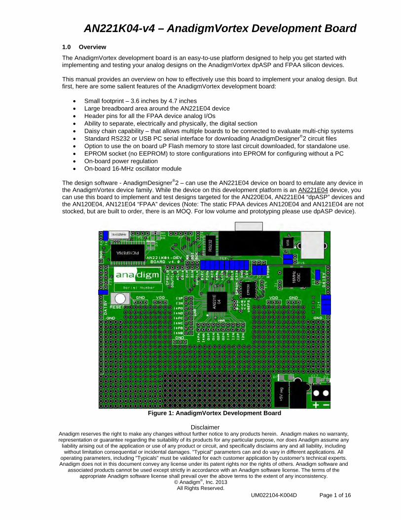
The AnadigmVortex development board is an easy-to-use platform designed to help you get started with implementing and testing your analog designs on the AnadigmVortex dpASP and FPAA silicon devices. This manual provides an overview on how to effectively use this board to implement your analog design. But first, here are some salient features of the AnadigmVortex development board:
Small footprint – 3.6 inches by 4.7 inches Large breadboard area around the AN221E04 device Header pins for all the FPAA device analog I/Os Ability to separate, electrically and physically, the digital section Daisy chain capability – that allows multiple boards to be connected to evaluate multi-chip systems Standard RS232 or USB PC serial interface for downloading AnadigmDesigner®2 circuit files Option to use the on board uP Flash memory to store last circuit downloaded, for standalone use. EPROM socket (no EEPROM) to store configurations into EPROM for configuring without a PC On-board power regulation On-board 16-MHz oscillator module
The design software - AnadigmDesigner®2 – can use the AN221E04 device on board to emulate any device in the AnadigmVortex device family. While the device on this development platform is an AN221E04 device, you can use this board to implement and test designs targeted for the AN220E04, AN221E04 “dpASP” devices and the AN120E04, AN121E04 “FPAA” devices (Note: The static FPAA devices AN120E04 and AN121E04 are not stocked, but are built to order, there is an MOQ. For low volume and prototyping please use dpASP device).
Figure 1: AnadigmVortex Development Board
Disclaimer
Anadigm reserves the right to make any changes without further notice to any products herein. Anadigm makes no warranty, representation or guarantee regarding the suitability of its products for any particular purpose, nor does Anadigm assume any
liability arising out of the application or use of any product or circuit, and specifically disclaims any and all liability, including without limitation consequential or incidental damages. "Typical" parameters can and do vary in different applications. All
operating parameters, including "Typicals" must be validated for each customer application by customer's technical experts. Anadigm does not in this document convey any license under its patent rights nor the rights of others. Anadigm software and
associated products cannot be used except strictly in accordance with an Anadigm software license. The terms of the appropriate Anadigm software license shall prevail over the above terms to the extent of any inconsistency.
© Anadigm®, Inc. 2013 All Rights Reserved.
AN221K04-v4 – AnadigmVortex Development Board
UM022104-K004D Page 2 of 16
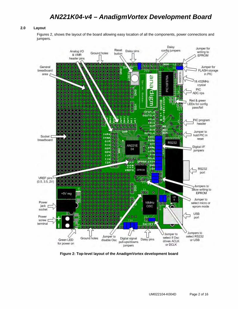
2.0 Layout
Figures 2, shows the layout of the board allowing easy location of all the components, power connections and jumpers.
Figure 2: Top-level layout of the AnadigmVortex development board

AN221K04-v4 – AnadigmVortex Development Board
UM022104-K004D Page 3 of 16
3.0 Powering up the AnadigmVortex Development Board
The options for powering up the board are as follows: Connect a transformer with centre voltage between +5.5V and +20V to the jack socket input, OR Connect wires from a single precision, regulated supply to the on-board 2-way terminal with the voltage
set to between 5.5V and 20V. Anadigm recommends the use of a standard supply regulator or d.c. power supply 6, 9, or 12 volt d.c.
regulated output. NOTE: the board is protected against connection to a supply with the wrong polarity WARNING: the board should not be powered with more than 20V
There is a green LED to indicate that the board is successfully powered up. The board should take approximately 25mA when first powered up and before the FPAA is configured. The current after the FPAA is configured depends very much on the circuit programmed into the FPAA and any additional circuitry added to the breadboard.
4.0 Programming the Board
Once the board has been powered up, simply connect the board to the serial port of a PC using a standard RS232 cable or USB cable. It is possible to physically connect both the RS232 and USB cables at the same time, however only one or the other is needed; please choose one and set the 2 shorting links on J15 appropriately. Anadigm prefers the RS232 because it is hardware detected and automatically discovered by AnadigmDesigner®2. We understand that many new PCs do not have RS232 interfaces and so have added a USB interface and all the complexity associated with drivers.
4.1 Programming the Board (serial Interface – RS232)
Once the board has been powered up, simply connect the board to the serial port of a PC using a standard RS232 cable.
Open AnadigmDesigner®2 on the PC, create a circuit and click on Configure/write to serial port. If configuration is successful, the green LED next to the PIC in the digital section will illuminate.
If the red LED illuminates then the configuration failed. If this happens then check the supply to the board and check that the pins marked VDD have +5V on them. Also check that the jumpers are in their default state (see figure 7 in section 7). Press the reset button and try again.
If configuration was successful then the circuit created in AnadigmDesigner®2 will be programmed into the dpASP. The analog inputs and outputs can be accessed via the header pins that surround the dpASP. Note that the outer rings of pins are connected to the dpASP analog I/Os, the inner ring of pins are all connected to VMR which is at analog signal ground (+2V).

AN221K04-v4 – AnadigmVortex Development Board
UM022104-K004D Page 4 of 16
4.2 Programming the Board (USB serial Interface)
Introduction
The AN221K04-DEV Ver4 board uses a Silicon Labs USB to UART Bridge, this device uses a standard USB cable, installs like a USB port but internally to the PC and software it appears as a Serial port.
Driver Installation
Do not connect the AN221K04-DEV Ver4 board to your PC via the USB cable - the driver must be installed first.
It is assumed that AnadigmDesigner®2 is already installed and registered on your PC.
To install the drivers (CP210x_Drivers.exe) included on the AnadigmDesigner®2 CD. You can also find the driver here http://www.anadigm.com/sup_downloadcenter.asp?tab=des&offset=15
If this is your first use and you do not have any previous drivers installed start from 3) below.
1) Unplug any USB connected AN221K04-DEV Ver4 board and if applicable other Anadigm product or SiliconLabs CP210x devices.
2) Remove old drivers that have previously been installed. For Windows systems, open the Add or Remove Programs window from the Control Panel. Next, select each CP210x entry and click on Remove.
3) Run the driver executable, CP210x_Drivers.exe, to extract the device drivers included with this release (this application is tested with Windows Only). The default installation directory for these extracted files is "C:\Silabs\Mcu\CP210x". To complete the driver installation……..
4) Connect the AN221K04-DEV Ver4 board and power it.
5) Install the new drivers. For Windows systems, the Add New Hardware Wizard should open when this new device is detected. Use the wizard to install the drivers by directing it to the "C:\SiLabs\MCU\CP210x\WIN" directory created in step 3.
The hardware wizard will install CP210x Composite device, then the CP2102 USB to UART Bridge Controller Drivers.
The drivers are now installed, connect a powered AN221K04-DEV board, start the AnadigmDesigner®2, from your desktop and check the connection from AnadigmDesigner2 on you PC to the AN221K04-DEV Ver4 board is working correctly. From within AnadigmDesigner2, go to “settings/preferences” and choose the “Port” Tab. If the installation has been successful the dropdown Port select menu will allow you to select COM* - CP2101 USB to UARF Bridge Controller, (COM* - * this number will be depend on you PC configuration).
NOTE: Driver installation and Port selection is only needed ONCE. If you subsequently plug into a different USB controller on your PC you may need to repeat step 5.
Board use – following driver installation is same as with the RS232 port.
Open AnadigmDesigner®2 on the PC, create a circuit and click on Configure. If configuration is successful, the green LED next to the PIC in the digital section will illuminate.
If the red LED illuminates then the configuration failed. If this happens then check the supply to the board and check that the pins marked VDD have +5V on them. Also check that the jumpers are in their default state (see figure 7 in section 7). Press the reset button and try again.
If neither LED illuminates and AnadigmDesigner®2 reports a communication error, then check from AnadigmDesigner2.
If configuration was successful then the circuit created in AnadigmDesigner®2 will be programmed into the dpASP. The analog inputs and outputs can be accessed via the header pins that surround the dpASP.
Note that the outer ring of pins are connected to the analog I/Os, the inner ring of pins are all connected to VMR which is at analog signal ground (+2V).
AN221K04-v4 – AnadigmVortex Development Board
UM022104-K004D Page 5 of 16
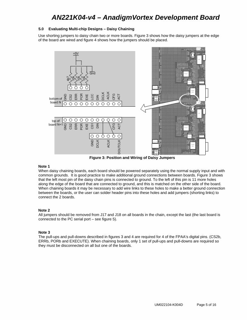
5.0 Evaluating Multi-chip Designs – Daisy Chaining
Use shorting jumpers to daisy chain two or more boards. Figure 3 shows how the daisy jumpers at the edge of the board are wired and figure 4 shows how the jumpers should be placed.
Figure 3: Position and Wiring of Daisy Jumpers
Note 1 When daisy chaining boards, each board should be powered separately using the normal supply input and with common grounds. It is good practice to make additional ground connections between boards. Figure 3 shows that the left most pin of the daisy chain pins is connected to ground. To the left of this pin is 11 more holes along the edge of the board that are connected to ground, and this is matched on the other side of the board. When chaining boards it may be necessary to add wire links to these holes to make a better ground connection between the boards, or the user can solder header pins into these holes and add jumpers (shorting links) to connect the 2 boards.
Note 2 All jumpers should be removed from J17 and J18 on all boards in the chain, except the last (the last board is connected to the PC serial port – see figure 5).
Note 3 The pull-ups and pull-downs described in figures 3 and 4 are required for 4 of the FPAA’s digital pins. (CS2b, ERRb, PORb and EXECUTE). When chaining boards, only 1 set of pull-ups and pull-downs are required so they must be disconnected on all but one of the boards.
AN221K04-v4 – AnadigmVortex Development Board
UM022104-K004D Page 6 of 16
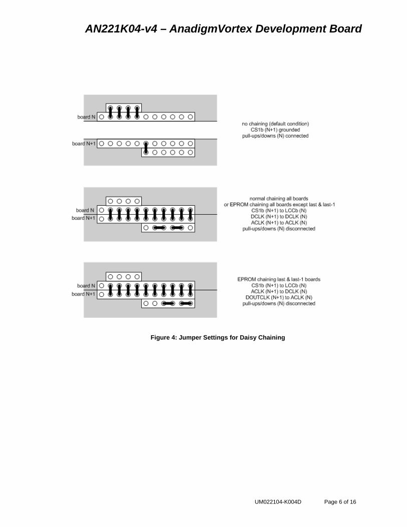
Figure 4: Jumper Settings for Daisy Chaining
AN221K04-v4 – AnadigmVortex Development Board
UM022104-K004D Page 7 of 16
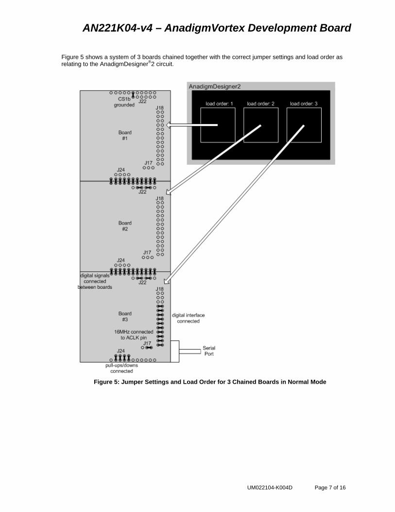
Figure 5 shows a system of 3 boards chained together with the correct jumper settings and load order as relating to the AnadigmDesigner®2 circuit.
Figure 5: Jumper Settings and Load Order for 3 Chained Boards in Normal Mode
AN221K04-v4 – AnadigmVortex Development Board
UM022104-K004D Page 8 of 16
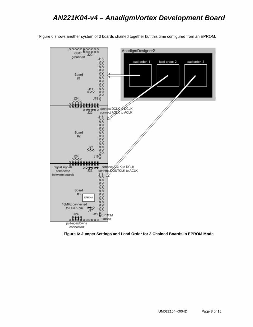
Figure 6 shows another system of 3 boards chained together but this time configured from an EPROM.
Figure 6: Jumper Settings and Load Order for 3 Chained Boards in EPROM Mode

AN221K04-v4 – AnadigmVortex Development Board
UM022104-K004D Page 9 of 16
6.0 Other Features
6.1 VREF Pins The 3 reference pins on the FPAA device – VMR (+2.0V), VREFP (+3.5V) and VREFN (+0.5V) – have been connected via the p.c.b. tracks to the 3 holes below the FPAA. In addition, VMR is available on 2 rows of pins that are adjacent to the analog I/Os. These reference voltages are not designed to provide current. 6.2 Header Pins All of the analog I/Os of the FPAA are brought out to header pins for easy connection. Next to these header pins is a second row of header pins connected to buffered VMR (+2V). This allows the user to connect any FPAA analog I/O to VMR using shorting jumpers, resistor jumpers of capacitor jumpers. Note: Connecting (via a short) active output pins to VMR is not recommended and may result is damage to the device. 6.3 EPROM There is a SPI EPROM socket (add you own pre-programmed SPI EEPROM) in the analog section of the board between the FPAA and the oscillator module. To put the board into EPROM mode, starting from the default jumper position (see figure 7):
1. Put a jumper onto J19 which sits right next to the EPROM socket. This makes the MODE pin of the FPAA high (EPROM mode).
2. Place a jumper on J26 to disable the PIC and remove the PORb jumper from J18. Alternatively one can remove all the jumpers from J18.
3. Put the jumper J17 in the left position (away from the USB socket) to allow the 16MHz oscillator module to drive the DCLK pin. In EPROM mode the 16MHz oscillator module drives the DCLK pin of the FPAA instead of the ACLK pin as normal (when daisy chaining boards, this only applies to the first board in the chain).
Power up the board and it will configure from the EPROM. Resetting the board will also cause it to be configured from the EPROM. Note that there will be NO LEDs illuminated to show that the configuration was successful. This is because the LEDs are driven by the PIC and this is disabled when booting from EPROM. Note that an EPROM integrated circuit is not supplied with this Development Kit. If you wish to use an SPI EPROM, source one and place it in to the socket on the board. An example of a compatible SPI EPROM is the Atmel AT25080. As a new feature for this AN221E04 development board, rev4 only. The board and AnadigmDesigner2 can be used to write to a fitted EEPROM. An EPROM can be programmed by the user using any compatible programmer and then fitted into the socket. Alternatively follow the procedure below, starting with the jumpers in their default positions (see figure 7). This procedure involves first creating the desired circuit in AnadigmDesigner®2 and storing it to the PIC’s FLASH memory (see section 6.6), then transferring the configuration data from PIC FLASH to the EPROM. 1. Remove the jumper from J6 to enable PIC storage and download the desired circuit to the board from
AnadigmDesigner®2. At the same time that the circuit was stored in the PIC, it was also downloaded to the FPAA. Check that the green LED is on to indicate a successful configuration.
2. Press the reset button briefly or power cycle the board, the circuit should automatically be reloaded to the FPAA from the PIC and the green LED should light. Writing to EPROM can only be done if storage to the PIC’s FLASH was successful, so it is important to do a reset or power cycle to check this.
3. Power down the board and move the 3 jumpers on J2 to the right (towards the RS232 socket). 4. Place a jumper on J4. This will enable writing to EPROM. 5. Power up the board. The data stored in the PIC’s FLASH will be transferred to the EPROM. If data was
transferred then the green LED will flash 5 times. If no data was transferred (because there was no data in the PIC) then the red LED will flash 5 times.
6. Power down the board and move the 3 jumpers on J2 back to the left (away from the RS232 socket).
* NOTE: before configuring the board, a setting needs to be changed in AnadigmDesigner®2 if the circuit is to be stored in EPROM. To change this setting, go to the Settings menu in AnadigmDesigner®2, select Active Chip Settings, then select the Chip tab. In the pull-down menu under Interface Options select “Mode pin is connected to VDD. Analog clock source: DCLK, PROM clock output: ACLK””. Click on OK. Then configure the board. If an EPROM programmer is used to program the EPROM, this setting still needs to be changed in AnadigmDesigner®2 before generating the data for programming into the EPROM.
Now follow the procedure for configuring from EPROM:

AN221K04-v4 – AnadigmVortex Development Board
UM022104-K004D Page 10 of 16
7. Place a jumper on J19 which sits right next to the EPROM socket. 8. Place a jumper on J26 to disable the PIC. Alternatively one can remove all the jumpers from J18. 9. Move the jumper on J17 to the left (away from the USB socket). Power up the board to check that it configures from the EPROM. Check that the circuit is functional because there is no LED indication for configuring from EPROM. Pressing the reset button briefly will reload the circuit. 6.4 Reset Button There is a reset button above the FPAA. This resets both the FPAA and the PIC (digital section). In EPROM mode, press the reset button to load the circuit from the EPROM into the FPAA. 6.5 Digital Section The digital section of the evaluation board is provided only so that there is a convenient (serial) interface from the board to a PC to enable direct configuration of the FPAA from AnadigmDesigner®2, normal use of the FPAA does not require this digital interface, the FPAA can be programmed directly from a SPI interface. It is convenient when first developing an analog circuit within the FPAA to have the direct interface to AnadigmDesigner®2, when the circuit(s) are implemented into a final design either a host uP (or DSP) or an EEPROM is normally used to store and configure the FPAA. The digital section of the board consists of a RS-232 transceiver, a USB transceiver and a PIC microcontroller (to perform serial ASCII to bit conversion). It also includes a green LED (to indicate successful configuration), and a red LED (to indicate failed configuration). The digital section sits along the right side of the board and is connected to the rest of the board by a set of jumpers J18. It is possible to cut away the digital section to leave a purely analog board with header pins on the edge to provide an external digital interface. If the digital section of the development board is removed or ignored (by pulling jumpers J18 or adding a jumper to J26), the FPAA can be configured directly using any processor with a SPI interface (or port configured with appropriate signals) by connecting signals directly to the FPAA side of J18. Fully dynamic control of the FPAA’s analog circuitry can be realised under software control via this connection. Note Anadigm® does not recommend any specific processor/controllers – our products work with most processors. Anadigm® recommends that our customers use their own processor development boards and connect via jumper J18 to Anadigm’s FPAA for fully dynamic control of the FPAA, in preference to re-engineering the digital section of this development board. Note 2 The lowest 5 pins of J18 form a standard SPI interface (the board is a SPI slave and should be connected to a SPI master). These pins consist of power and ground, CS2b which should be connected to SSb, DCLK which should be connected to SCK, and DIN which should be connected to SO of the SPI master or MOSI. 6.6 FLASH Storage In FLASH storage mode, all primary configurations sent to the development board are stored in the FLASH memory of the PIC. The last configuration sent will be remain stored. This means that after the board has been configured, it will remember the last configuration it was sent after being reset or board power being cycled off and on. Note that when chaining boards, the primary configurations for all devices in the chain will be stored. Reconfigurations (updates) are not stored. FLASH storage is enabled by removing the jumper from J6. The FLASH memory can be cleared by briefly shorting the jumper J6. If FLASH storage of primary configurations is not wanted then a jumper should be placed permanently on J6 to disable this feature. Note that FLASH storage can slow down board configuration and this can cause problems with some PC serial interfaces.
AN221K04-v4 – AnadigmVortex Development Board
UM022104-K004D Page 11 of 16
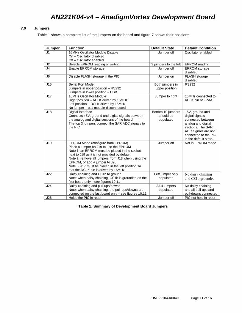
7.0 Jumpers
Table 1 shows a complete list of the jumpers on the board and figure 7 shows their positions.
Jumper Function Default State Default Condition J1 16MHz Oscillator Module Disable
On – Oscillator disabled Off – Oscillator enabled
Jumper off Oscillator enabled
J2 Selects EPROM reading or writing 3 jumpers to the left EPROM reading J4 Enable EPROM storage Jumper off EPROM storage
disabled J6 Disable FLASH storage in the PIC Jumper on FLASH storage
disabled J15 Serial Port Mode
Jumpers in upper position – RS232 Jumpers in lower position – USB
Both jumpers in upper position
RS232
J17 16MHz Oscillator Module Right position – ACLK driven by 16MHz Left position – DCLK driven by 16MHz No jumper – osc module disconnected
Jumper to right 16MHz connected to ACLK pin of FPAA
J18 Digital Interface Connects +5V, ground and digital signals between the analog and digital sections of the board. The top 3 jumpers connect the SAR ADC signals to the PIC
Bottom 10 jumpers should be populated
+5V, ground and digital signals connected between analog and digital sections. The SAR ADC signals are not connected to the PIC in the default state.
J19 EPROM Mode (configure from EPROM) Place a jumper on J19 to use the EPROM Note 1: an EPROM must be placed in the socket next to J19 as it is not provided by default. Note 2: remove all jumpers from J18 when using the EPROM, or add a jumper to J26. Note 3: J17 must be placed in the left position so that the DCLK pin is driven by 16MHz.
Jumper off Not in EPROM mode
J22 Daisy chaining and CS1b to ground Note: when daisy chaining, CS1b is grounded on the first board only – see figures 10,11
Left jumper only populated
No daisy chaining and CS1b grounded
J24 Daisy chaining and pull-ups/downs Note: when daisy chaining, the pull-ups/downs are connected on the last board only – see figures 10,11
All 4 jumpers populated
No daisy chaining and all pull-ups and pull-downs connected
J26 Holds the PIC in reset Jumper off PIC not held in reset
Table 1: Summary of Development Board Jumpers
AN221K04-v4 – AnadigmVortex Development Board
UM022104-K004D Page 12 of 16
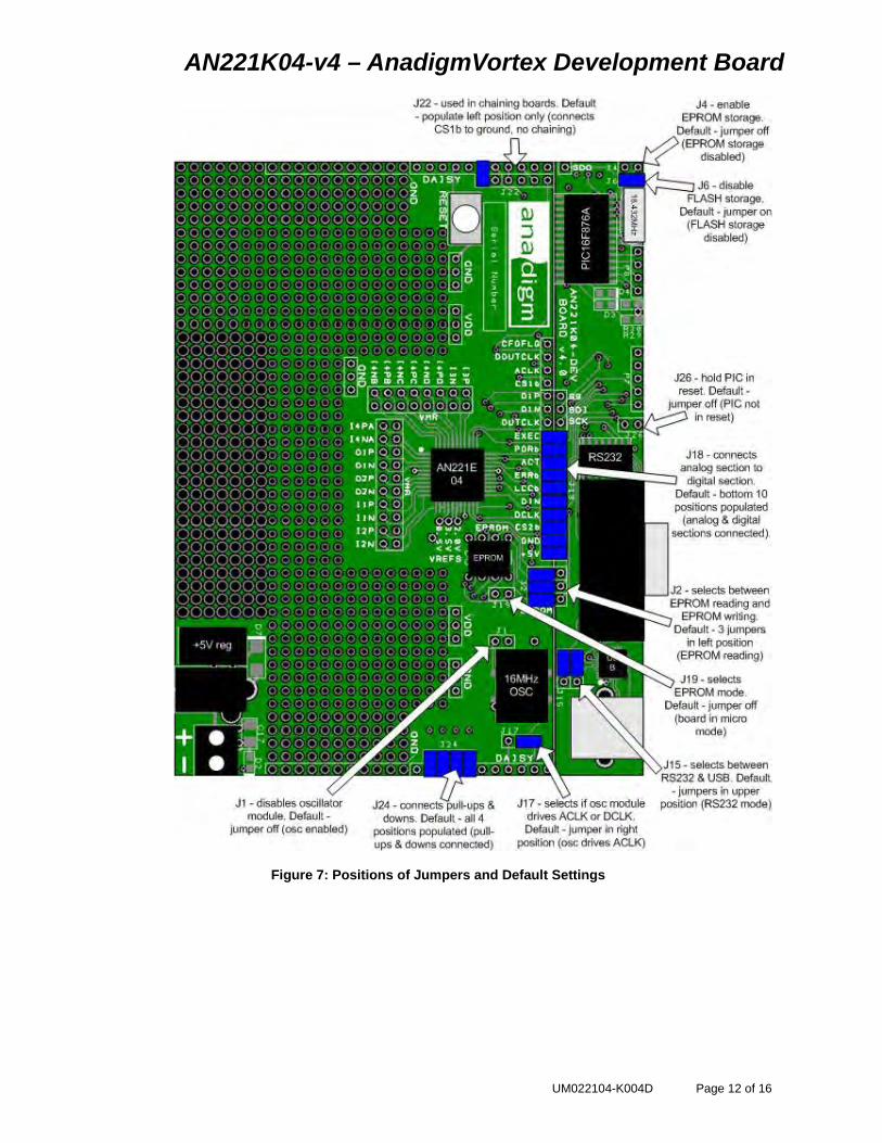
Figure 7: Positions of Jumpers and Default Settings

AN221K04-v4 – AnadigmVortex Development Board
UM022104-K004D Page 13 of 16
8.0 Absolute Maximum Ratings
Parameter Symbol Min Typ Max Unit Comment
DC Power Supply
3.5mm jack socket
Vjack 5.5 12 20 V DC voltage only, must be regulated
Centre pole is positive, outer sleeve is ground
DC Power Supply
screw terminal
V+ +5.5 +6 +20 V DC voltage only, must be regulated
Voltage is relative to “Gnd” post
FPAA Input Voltage Fin -0.5 +5.5 V Direct input to FPAA on analog IO header pins or digital pins (J18)
FPAA Output Voltage Fout -0.5 +5.5 V Direct output from FPAA on analog IO header pins or digital pins (J18)
RS-232 Input Voltage Rin -30 +/-10 +30 V Standard RS-232 signal levels
RS-232 Output Voltage Tout -15 +/-10 +15 V Standard RS-232 signal levels
USB Input Voltage D+/- +4.75 +5 +5.25 V Standard USB signal levels
USB Output Voltage D+/- +4.75 +5 +5.25 V Standard USB signal levels
Operating Temperature Top 10 50 oC Ambient Operating Temperature
Storage Temperature Tstg -20 70 oC Ambient Storage Temperature

AN221K04 – the AnadigmVortex Development Board
UM022104-K004D Page 14 of 16

AN221K04 – the AnadigmVortex Development Board
UM022104-K004D Page 15 of 16

AN221K04 – the AnadigmVortex Development Board
UM022104-K004D Page 16 of 16
Notes: For More information Contact
http://www.anadigm.com [email protected]