an spm based tester for the study of micro …...an spm based tester for the study of micro-contacts...
TRANSCRIPT
1
AN SPM BASED TESTER FOR THE STUDY
OF MICRO-CONTACTS
A THESIS
PRESENTED BY
NIKHIL JOSHI
TO
THE DEPARTMENT OF
MECHANICAL AND INDUSTRIAL ENGINEERING
In the partial fulfillment of the requirements
for the degree of
MASTER OF SCIENCE IN MECHANICAL ENGINEERING
IN THE FIELD OF
MECHANICS AND DESIGN
NORTHEASTERN UNIVERSITY
BOSTON MA
August 2010

2
Abstract
The testing of micro-contacts at low forces (below 1mN) is critical for understanding the contact
evolution of MEMS contact-switches. Testing is achieved with a specially designed micro-
contact-test assembly based on an AFM. The micro-contact-test assembly consists of a Si force
sensor with an integrated micro-bump and a mating silicon pillar. Both sides of the contact can
be coated with various combinations of metals to provide a wide range of metal-contact pairs for
testing. When fabricated with different lengths, these force sensors cover a wide range of forces
from 10µN to 1mN. Both force and resistance can be measured simultaneously during the
contact tests. To protect the contacts from contamination, assemblies were first cleaned using Ar
and O2 plasmas, or UV/ozone, followed by testing under a constant stream of nitrogen. Cleaning
efficiencies of Ar and O2 plasma, and UV/ Ozone were compared by performing in-situ and ex-
situ experiments on a variety of metal-pairs. Experiments were conducted on Au, Ru, Ir and
V2O5-Au, and Au-Ni with three different compositions under different forces. It is proposed that
integration of electrical properties of Au with the mechanical properties of Ru can promote an
electromechanically sound and long lasting metal contact pair. Two strategies were followed to
verify this proposition 1) using a layered stack of Ru of different thicknesses on Au for the entire
test assembly 2) using a Au-coated force sensor over a Ru-coated pillar for conducting contact
tests. The simulation results for the four-wire resistances of contacts using finite element analysis
show good agreement with the recordings from the system.

3
Acknowledgements
I would like to thank all the people who have supported me mentally and academically while
successfully completing this work.
First of all I am extremely thankful to my advisor Professor George Adams and co-advisor
Professor Nicol McGruer for providing me with the opportunity to work on this project.
Professor Adams has always been the source of inspiration for me. His solid knowledge in the
field of contact mechanics helped me learn behavior of different metal-contact pairs. Professor
McGruer was always supportive while constructing the system. His knowledge of electronics
was vital in every aspect of the project.
I am thoroughly grateful to Dr. Lei Chen. Without his guidance and motivation, completion of
this thesis would have been very difficult. His previous experience in testing of micro-contacts
helped me rapidly learn different issues related with different metal-pairs and also while doing
simulations using Ansys.
I also want to thank Ana Maria Pinto and Dr. Juan Aceros for guiding me while building the
system. I was very fortunate to get the training on AFM from Peter Ryan. His role was very
important while learning the calibrations required for the system.
The last but the most important acknowledgement belongs to Scott McNamara. He was always
ready to help us and solve the problems related to different gasses and tube fittings. His help in
clean-room has always been of a great value.
I specially appreciate the support given by all my friends and relatives.

4
Table of Contents
Table of Contents _____________________________________________________________ 4
Table of Figures ______________________________________________________________ 6
Chapter 1: - Introduction
1.1 The Beginning of RF MEMS _________________________________________________ 8
1.2 An Overview of MEMS Switches ____________________________________________ 10
1.3 Types of Switches _________________________________________________________ 12
1.4 Failure Mechanisms and Testing Background ___________________________________ 14
1.5 Background ______________________________________________________________ 18
1.6 Contact Preparation ________________________________________________________ 20
Cleaning Mechanism ______________________________________________________ 22
1.6.1 UV/ Ozone Cleaning _____________________________________________________ 22
Basics:- _______________________________________________________________ 22
1.6.2 Plasma Cleaning_________________________________________________________ 24
1.7 Testing Background _______________________________________________________ 27
Chapter 2: - Set-Up
2.1 Purpose of the Set-Up ______________________________________________________ 28
Contributions ____________________________________________________________ 29
2.2 Key Features of the Set-Up __________________________________________________ 30
2.2.1 JEOL SPM (Atomic Force Microscope) ______________________________________ 30
2.2.2 Force Sensor____________________________________________________________ 31
2.3 Mechanical Set-Up ________________________________________________________ 34
2.3.1 Vacuum System and Plasma Source Generator: - _______________________________ 34
2.3.2 Lifting System: - ________________________________________________________ 36
2.3.3 Nitrogen Flow Assembly for Ambient Control:- ________________________________ 37
2.4 Electrical Set-Up __________________________________________________________ 38
Set-Up for Piezo __________________________________________________________ 40
2.5 Testing Procedure _________________________________________________________ 43
2.5.1 Procedure for Testing _____________________________________________________ 45
Steps _________________________________________________________________ 45
5
2.5.2 Procedure for Plasma Cleaning _____________________________________________ 47
Chapter 3: - Simulation
3.1 Simulation of Pure Au-Au Contact ____________________________________________ 50
3.2 Simulation of Layered Ru ___________________________________________________ 55
Chapter 4: - Discussion of Data and Results
4.1 Au_Au: - ________________________________________________________________ 60
Types of Failures Observed in Au-Au Contact During Cycling Tests: - _______________ 70
4.2 Ru_Ru & Ir_Ir ____________________________________________________________ 71
4.3 Au_Ru & Au_Ir __________________________________________________________ 78
4.4 Vanadium Oxide __________________________________________________________ 83
4.5 Au-Ni Alloys _____________________________________________________________ 85
Chapter 5:- Conclusions _______________________________________________________ 87
Chapter 6:- Future Work ______________________________________________________ 95
Appendix
A. Calculation for Nitrogen Flow Control _________________________________________ 92
B. Calculations for Designing Roughing Hose Diameter ______________________________ 94
C. Vacuum Chamber __________________________________________________________ 97
D. Lifting Structure ___________________________________________________________ 98
E. Tube and Holder Fittings for Nitrogen Flow Control _____________________________ 104
Bibliography _______________________________________________________________ 100

6
Table of Figures
Figure 1.1 MEMS Market Forecast ______________________________________________________ 8
Figure 1.2 RF MEMS Switch Market Taken from (38) _______________________________________ 10
Figure 1.3 Comparison of Technologies Taken from (39) ____________________________________ 11
Figure 1.4 Classification of MEMS Switches ______________________________________________ 13
Figure 1.5 Contact Failure Due to High Pull-off Force ______________________________________ 15
Figure 1.6 Contact Failure Due to Contamination _________________________________________ 17
Figure 1.7 Plasma Cleaning Mechanism _________________________________________________ 25
Figure 2.1 Basic Functioning of AFM Showing Path of the Laser Beam and PD Segments Taken from
SPM Manual (37) ___________________________________________________________________ 30
Figure 2.2 SEM Image of Force Sensor __________________________________________________ 31
Figure 2.3 SEM Image of Pillar ________________________________________________________ 31
Figure 2.4 Design of the Force Sensor and Pillar for Conducting Four -Wire Resistance Measurement
Across Contact Area Taken from (40) ___________________________________________________ 33
Figure 2.5 Nitrogen-Ambient Control ___________________________________________________ 37
Figure 2.6 Two-Wire Resistance Measurement ____________________________________________ 38
Figure 2.7 Four-Wire Resistance Measurement ____________________________________________ 38
Figure 2.8 Electrical Set-Up ___________________________________________________________ 39
Figure 2.9 Schematic Diagram Showing Piezo Set-Up ______________________________________ 41
Figure 2.10 Piezo Expansion Model _____________________________________________________ 41
Figure 2.11 Schematic Diagram Showing Entire Set-Up _____________________________________ 42
Figure 2.12 AFM Image of the Calibration Sample _________________________________________ 43
Figure 2.13 Calibration Sample ________________________________________________________ 43
Table 2.1: - Spcecifications of the Force Sensors ___________________________________________ 34
Table 2.2: - Cycle-Frequency Table _____________________________________________________ 49
Figure 3.1 Schematic Diagram of the Model of Simple Metal-Metal Contact _____________________ 51
Figure 3.2 Meshing of Two 40µx40µx40µ Blocks in Contact With Each Other By Contact Area Having
a = 0.5µm Radius ___________________________________________________________________ 52
Figure 3.3 Simulation Results Showing Resistance vs Thickness Plot ___________________________ 53
Figure 3.4 Simulated Voltage-Distribution for the Model With Real Geometry ___________________ 54
Figure 3.5 Schematic Diagram of the Model Having Layered Structure _________________________ 55
Figure 3.6 Simulated Contact Radius vs Force by Eid(27) ___________________________________ 56
Figure 3.7 Simulated Contact Resistance vs Force for 10nm Ru Layered Over 500 nm Au and Model
Represented by Equation (3) ___________________________________________________________ 58
Figure 3.8 Simulated Contact Resistance vs Force for 50nm Ru Layered Over 500nm Au and Model
Represented by Equation (3) ___________________________________________________________ 58
Figure 3.9 Simulated Contact Resistance vs Force for 100nm Ru Layered Over 500nm Au and Model
Represented by Equation (3) ___________________________________________________________ 58
Figure 3.10 Simulated Contact Resistance vs Force for 300nm Ru Layered Over 500nm Au and Model
Represented by Equation (3) ___________________________________________________________ 58
Table 3.1 Simulated Contact Resistances for the Model With Real Geometry _____________________ 55
Table 3.2 Measured Resistivity Values for Different Thicknesses ______________________________ 56

7
Figure 4.1 Sample Signal Acquired from AFM ____________________________________________ 61
Figure 4.2 Au-Au Contact Resistance at Different Forces After ~10 Cycles ______________________ 63
Figure 4.3 Au-Au Contact Resistance When Cycled at Particular Forces as Shown by the Bold Dots __ 63
Figure 4.4 In-situ Plasma Cleaning Experiment on Au-Au Contact_____________________________ 66
Figure 4.5 Resistance vs Force Diagram Showing Effect of 15min In-situ O2 Plasma on Au-Au Contact 66
Figure 4.6 Au-Au Cleaning Effect of O2 Plasma Cleaning on Pull-off Force______________________ 68
Figure 4.7 Au-Au Cleaning Effect of O2 Plasma Cleaning on Contact Resistance__________________ 68
Figure 4.8 Au-Au Cycling Data Showing Resistance vs No. of Cycles ___________________________ 69
Figure 4.9 Au-Au Cycling Data Showing Pull-off Force vs No. of Cycles ________________________ 69
Figure 4.10 Sliding Occurring at Au-Au Contact Due to Misalignment _________________________ 70
Figure 4.11 Au-Au Contact Showing High Pull-off Force During Cycling _______________________ 70
Figure 4.12 Au-Au Contact Ductile Separation ____________________________________________ 70
Figure 4.13 Ru & Ir Contact-Failures During Cycling ______________________________________ 71
Figure 4.14 In-situ Plasma Cleaning of Ru-Ru Contact at 1 Hz _______________________________ 72
Figure 4.15 Ex-situ Ar Plasma Cleaning Effect on Ru-Ru Contact Resistance ____________________ 74
Figure 4.16 Ru Contact Cycled at 500 µN After Ar Plasma Treatment __________________________ 74
Figure 4.17 Ex-situ O2 Plasma Cleaning Effect on Ru-Ru Contact Resistance ____________________ 75
Figure 4.18 Cleaning Effect of O2 Plasma on Ru-Ru at 100µN ________________________________ 76
Figure 4.19 Cycling Data of Ru-contact After O2 Plasma Treatment ___________________________ 76
Figure 4.20 Comparison of Three Cleaning Methods _______________________________________ 77
Figure 4.21 Cycling Data of Ir Contact After O2 Plasma Treatment ____________________________ 77
Figure 4.22 Cycling Data of Au-Ir ______________________________________________________ 79
Figure 4.23 Au-Ru Low-Force Contact Resistance Measurement ______________________________ 79
Figure 4.24 Au-Ru Cycled at 100 µN ____________________________________________________ 79
Figure 4.25 Comparison of All Materials After O2 Plasma Cleaning ___________________________ 80
Figure 4.26 Distribution of Contact Resistance Data of Layered Au/Ru _________________________ 81
Figure 4.27 Comparison of Au-Ru With Layered Au/Ru _____________________________________ 82
Figure 4.28 Au/ V2O5 Showing Effect of O2 Plasma Cleaning _________________________________ 84
Figure 4.29 Au/ V2O5 Cycling Data _____________________________________________________ 84
Figure 4.29 Au/V2O5 Cycling Data ______________________________________________________ 85
Figure 4.30 Au-Ni Alloys’ Contact Resistance Comparison After O2 Plasma Cleaning _____________ 85
Figure 4.31 Au-Ni Alloys’ Cycling Data Resistance vs No. of Cycles ___________________________ 85
Figure 4.32 Au-Ni Alloys’ Cycling Data Pull-off Force vs No. of Cycles ________________________ 85
Figure A1 Concentration Profile _______________________________________________________ 93
Figure C1 Plasma Chamber ___________________________________________________________ 97
Figure D1 Lifting Structure ___________________________________________________________ 98
Figure E1 Drawing of the Clamp Fixed Inside AFM for Holding N2 Tube Near Contact ____________ 99
Figure E2 Drawing of Tube Carrying N2 Near Contact ______________________________________ 99

8
Chapter 1-Introduction
1.1 The Beginning of RF MEMS
MEMS technology is approximately forty years old and it has seen a wide improvement in its
scope and usability. It covers wide applications, from pressure sensors, temperature sensors
accelerometers switches, pumps etc. Figure 1.1 gives an idea of the different fields that are
influenced by the MEMS technology (44). MEMS switches were first developed in 1980s and
then for a long time it was in research phase. MEMS switch for microwave applications was first
developed in 1990-91 by Dr. Larry Larson at the Hughes Research Labs (1). Even though the
Figure 1.1 MEMS Market Forecast

9
technology had poor reliability and yield, it demonstrated promising performance than GaAs
devices. This was the breakthrough in MEMS switch technology which caught the interest of
different research groups and companies. The Rockwell Science Center gave rise to metal-to-
metal contact switch while the one from Texas Instruments was of capacitive type. It took the
mid and late 1990s to reach the MEMS switch-research at the university level when the
University of Michigan, Northeastern University, University of California at Berkeley, MIT
Lincoln Labs, and Columbia University got involved for improving the technology. By 2001
there were more than 30 companies such as Analog Devices, Motorola, and Samsung working in
this area (1).
Main reason behind RF MEMS switch's rapid growth since the 1990s was that the
semiconductor switching diodes could not improve more as compared to MEMS switches as far
as the cutoff frequency was concerned. The cutoff frequency of silicon CMOS was improved
from 500 MHz to 100 GHz, GaAs HEMT devices were improvement from 10-20 GHz to above
800 GHz while cutoff frequency of the InP p-i-n diodes could increase from 500 GHz in 1985 to
2000 GHz in 2001. This demanded some new technology which can be used at higher
frequencies especially in defense applications. RF MEMS devices were proved promising even
at 40,000 GHz with low-loss applications (1).

10
1.2 An Overview of MEMS Switches
MEMS systems are the combination of
mechanical elements such as physically
moving beams or diaphragms and
electrical components used for actuation.
Electronic components are fabricated
using standard IC fabrication techniques
while mechanical components are
fabricated using compatible
micromachining techniques for selectively etching or adding the structures to form the structures
like beams. Figure 1.2 shows the increasing market value for RF MEMS in different
applications. The trend that was predicted in 2006, as shown in Figure 1.2, seems to be in
reasonable agreement with current market trends. It also gives us an idea of the increasing scope
of MEMS switch market in different industries. It has found a big scope in defense applications
and cell phone market because of their smaller size and higher cut-off frequency (2). These new
system can be prototyped as one powerful station sending signals to the local cell phones that can
act like the nodes of the network. The digital cellular and personal communications service
(PCS) work at 0.9 and 1.9 GHz, respectively which consists of the range of frequency spectrum
that is used for cellular purposes (3).
MEMS switches operating at RF frequencies do not actually have to switch at those frequencies.
However it implies the frequency of electrical signal that is supported by these switches. Hence
the micromechanical structures do the job of actuating the circuits when in physical contact and
breaking the circuit when not in contact. This is the main reason behind higher isolation and
Figure 1.2 RF MEMS Switch Market Taken from (38)

11
higher operating frequencies provided by
MEMS switches. Another advantage of this
technology is the low power consumption.
Many of the RF MEMS devices under research
are actuated electrostatically. So the current for
actuation is required only while performing
switching. This dynamic actuation lessens the
power consumption. MEMS switches are also recognized for their lower insertion loss. Figure1.3
compares MEMS with different technologies for their cost, power consumption and loss. Despite
of all these advantages, the RF MEMS has not yet able to replace its semiconductor counterparts
because of the few shortcomings. Physical movement of the mechanical structures required for
actuation puts limitation of switching speed of the switch. The electromechanical actuation time
is typically many microseconds or greater, which is substantially longer than typical electrical
time constants in semiconductor devices. Another major reason is the various types of failures
involved in metal-metal contact. Stiction and contamination-failure are the most prominent types
of contact failures. Stiction describes the phenomenon in which the top and bottom electrodes
bond together by microscopic surface forces particularly occurring in metal-metal contact
switches. It strongly depends on surface morphology. Contamination-failure is nothing but the
rise in contact resistance due to different chemical reaction taking place on contacting surfaces
during switching.
Figure 1.3 Comparison of Technologies
Taken from (39)

12
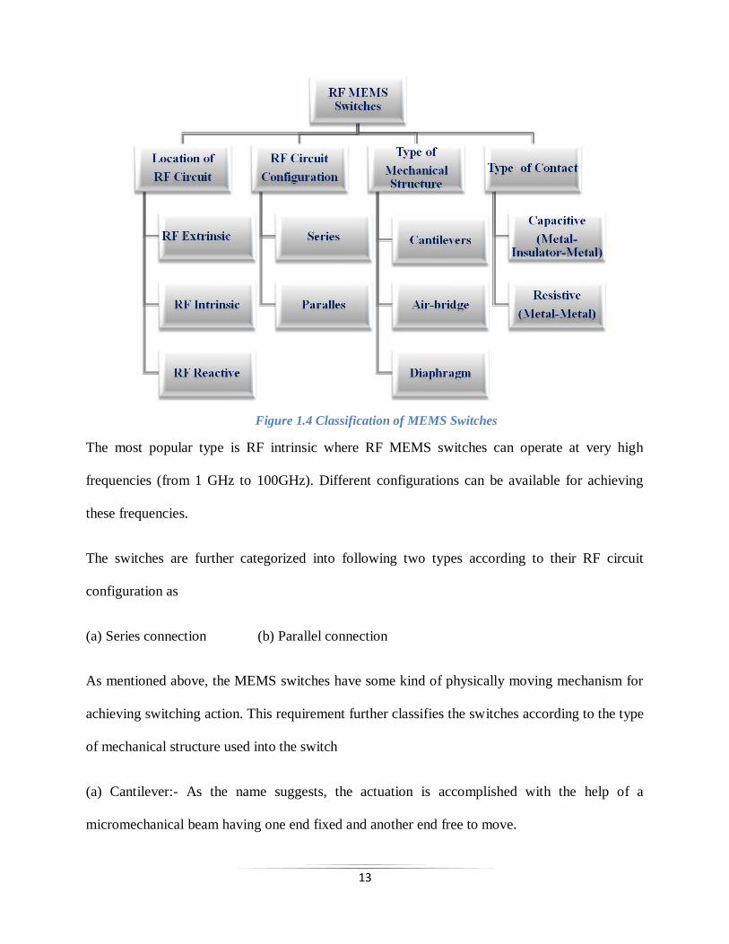
1.3 Types of Switches
‘MEMS switches’ is quite a broad term that consists of several types and designs. As explained
in (1), it is possible to build at least 32 different types of MEMS switches using different
actuation mechanisms, contacts and circuit implementations. A few of them will be discussed in
this section. Figure 1.4 displays the five of the important characteristics that classify MEMS
switches i.e. 1) Location of the RF circuit 2) Configuration of the RF circuit 3) Type of
mechanical structure used for actuation 4) Type of contact 5) Actuation Mechanism MEMS
switches are broadly categorized into following types depending on the location of RF circuit
(3).
1. MEMS structures that are located outside the RF circuit i.e. RF extrinsic
Examples:- Tunable micromachined transmission line
2. MEMS structures that are located inside the RF circuit i.e. RF intrinsic
Examples:- Electrostatically operated shunt switch
3. MEMS structures that has RF function couples to the actuation i.e. RF reactive
Example: - Micromechanical resonator
13
The most popular type is RF intrinsic where RF MEMS switches can operate at very high
frequencies (from 1 GHz to 100GHz). Different configurations can be available for achieving
these frequencies.
The switches are further categorized into following two types according to their RF circuit
configuration as
(a) Series connection (b) Parallel connection
As mentioned above, the MEMS switches have some kind of physically moving mechanism for
achieving switching action. This requirement further classifies the switches according to the type
of mechanical structure used into the switch
(a) Cantilever:- As the name suggests, the actuation is accomplished with the help of a
micromechanical beam having one end fixed and another end free to move.
Figure 1.4 Classification of MEMS Switches

14
(b) Air Bridge:- A thin strip of metal and dielectric forming a bridge is fixed at both ends and
suspended over free space in the middle.
(c) Diaphragm:- The diaphragm is a thin film-like structure usually made of metal that is fixed
at all of the edges while central area remains suspended.
Generally these are operated by using electrostatic actuation. Bias voltage applied between the
cantilever or diaphragm and the base surface creates an electrostatic force of attraction and pulls
down the suspended member at certain threshold voltage. Voltage can be reduced to bring it back
to original position.
Another important classification of MEMS switches from contact point of view is
(a) Capacitive: - It is also called as metal-insulator-metal and usually consists of membrane
which gets pulled down due to the voltage applied between the control electrode and membrane.
A dielectric layer provided on the control electrode keeps the membrane capacitively coupled.
This helps in reducing impedance between the upper and lower electrodes (4).
(b) Resistive: - These are normally metal-metal contact type switches either in the form of
cantilever or membrane. Most of the types of switches those are currently popular or under
research are of this type.
1.4 Failure Mechanisms and Testing Background
As explained in Chapter 1.1, MEMS contact switches have gained attention in the wireless
industry considering their advantages over capacitive switches as well as solid state devices such
as FETs and diodes. However none of the potential applications such as Tx/Rx antenna
15
switching, frequency band selection, tunable filters, and antenna reconfiguration etc. have been
materialized in high volume products to a large extent because of reliability concerns. Most of
the reliability issues are related to the metal contacts (4). Since MEMS contact switches
incorporate physically moving components which contact each other at particular force, it
becomes a challenging task to design a switch having such a metal-contact pair that will promise
all the required electro-mechanical characteristics for more number of cycles (~109). It is
therefore necessary to understand the typical failure mechanisms occurring in micro-contacts
during the switch-operation. Several attempts have been made in the past to study the micro-
contact evolution. However Chen (5) and Majumder (6) are the two of the most important
contributions. As it is studied by Chen (5), the most frequently observed types of failures in
typical MEMS switches are
1. Failure to open and 2. Failure to close
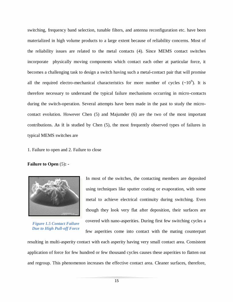
Failure to Open (5): -
In most of the switches, the contacting members are deposited
using techniques like sputter coating or evaporation, with some
metal to achieve electrical continuity during switching. Even
though they look very flat after deposition, their surfaces are
covered with nano-asperities. During first few switching cycles a
few asperities come into contact with the mating counterpart
resulting in multi-asperity contact with each asperity having very small contact area. Consistent
application of force for few hundred or few thousand cycles causes these asperities to flatten out
and regroup. This phenomenon increases the effective contact area. Cleaner surfaces, therefore,
Figure 1.5 Contact Failure
Due to High Pull-off Force

16
can show strong adhesion because of their higher surface energies (1 to 3 J/m2) as compared to
contaminated surface. The larger the contact-area the higher is the adherence force. Metals like
Au which are soft and lesser reactive get relatively quickly flattened out during cycling. So the
flat surface tries pull down the moving member of the switch. Hence the force of adhesion is also
termed as pull-off force.
Current passing through any metal conductor increases its temperature because of the voltage
applied and resistivity of contact-metals. Since, in microswitches, the contacting members have
very small cross sectional area, even small increase of current cause significant increase in
temperature and soften the nano-asperities. During switching action, the surface morphology
undergoes some changes due to the softening and hence contact area increases. Pull-off force
may eventually increase as explained above. Even the small voltage like 430mV can increase the
temperature of Au micro-contacts up to 10630
C and melt it. This melting makes the micro-
welding of contact spots and separation becomes difficult. The load applied to the microcontact
causes plastic yielding of the contact-metal. As the switching progresses, the cyclic loading and
unloading transfers some material from one side to another and reduces the scope of separation.
Ductile separation is another type of the failure occurring in metal-contacts due to higher applied
forces or higher contact adhesion. Both of these causes can rupture the micro-contact and deform
it plastically. During unloading, instead of pure separation, plastic yielding imposes neck
formation across the contact and nano-wires can be formed. These nano-wires or micro-bridges
keep the moving member electrically connected to the stationary part. Plastic yielding can also
cause material transfer and makes the switch unable to separate.
Failure while Hot Switching: - Usually current is allowed to flow across the contact only when
the switch is closed. Hot switching refers to the mode of operation when current is continuously

17
flowing across the contacting members even though they are in open state. High voltage applied
across the contact can cause arcing. This leads to the softening of contact-metal especially Au.
The contact fails due to increase in stiction or contact welding.
Failure to Close (5): -
This is mainly referred to as excessive increase in contact
resistance. This may occur due to the surface films present after
microfabrication processes. Normally these films are few
nanometers thick and can break down during cycling if slightly
higher force (> 100 μN) or higher current is applied. However the
refractory metals like Ru, Ir have higher affinity for the
hydrocarbons and they can also attract carbonaceous molecules from the atmosphere and act as
catalyst. These reactions build serious contamination and electrical resistance increases that
makes. The best way to prevent this kind of failure is to modify microfabrication processes so
that surface films will not exist. Methods such as plasma cleaning or UV/Ozone cleaning are
must before packaging to remove any traces of contaminants left during fabrication steps.
Controlling the ambient during packaging by using gasses like N2 or Ar is very crucial for
avoiding contamination.
Pitting and hardening of the metal contact area is another reason behind the increase in contact
resistance. As the two members coated with metal hit each other repeatedly at the same spot,
strain-hardening occurs at local contact-spots. This reduces contact area and eventually increases
contact resistance.
Figure 1.6 Contact
Failure Due to
Contamination

18
1.5 Background
All the modes of failure mentioned above are interconnected with each other and switch doesn't
always fail only because of one single reason. Different theories and observations made during
the experiments help us understand the causes of failure. Usually the MEMS contact-switches
that survive 108 to 10
9 cycles without significant increase in contact resistance (< 1 Ω) or contact
failure while operating at lower forces (~100 μN) are considered as reliable for the commercial
applications. Au has always been the favorite metal for contact switches because of its low
resistivity and nobleness. It has been widely used in the switches developed by different
companies such as Motorola, HRL, Omron and universities for e.g University of Illinois,
Northeastern University, University of Michigan, Lincoln labs at MIT(1). However contact-
stiction occurring in Au contacts has put some limitation on the life-time and reliability. Au is
also a very soft metal. Its softening temperature i.e. 1000C is achieved by applying merely 70mV
across the contact. Any temperature higher than that can lead the switch fail to open either
because of stiction and material transfer. Different groups have also tried materials such as Ru,
Rh, Ir alloys for avoiding the stiction problem but these metals are not easy to handle during
microfabrication steps. If the deposition conditions are not maintained, the thin films develop
high residual stress and buckle the original structure. These refractory metals also have strong
affinity for hydrocarbons. Hence, unlike Au, they get contaminated very quickly. Higher
electrical resistivity and material hardness are also two of the characteristics that make switch-
designing a tough task. So, the companies or research institutes have to make several
improvements in the switch design and fabrication for improving the life time for using Au as the
contact metal. These designs include ball-grid array and dimple designs (7), collapsing type
cantilevers (8), multiple contact-points by Duffy et al (1), and corrugated diaphragm (9), macro-

19
contact spots by Schimkat et al (1), and self cleaning lateral actuation (10). However research
has also been going on to find more reliable metal-contact pair that can replace gold so that the
switch design can be simple. Ru (9), Ir (11) Au-Ni alloys by Schimkat et al (1), Ru, Rh (12),
palladium multilayer structures (13), Rh and Au-Ni (8), platinum by Duffy et al (1) are some of
the examples of them.
For testing these materials under different conditions special test-facilities are required. These
test facilities generally use AFM (14), (5), nano-indenter (11), (15),(16),(17) or pico-indenter (8)
for measuring/controlling the force applied on the micro-contact. However most of them have
failed to test the contacts at lower forces. Cycling the contacts for more than 106
cycles is also an
important requirement of the facility. Although the systems constructed by Ma et al (8), Yunus
(16) and Kwon(11) are really good for comparing different material pairs, they have not
performed any cycling test, which does not confer the long term performance of respective
materials. Also, Ma et al(8) and Yang (14) directly use the upper cantilever from the
commercially available switches which puts limitation on using various metals for the upper side
of contact. On the other hand the test-stations by Gilbert et al(15) can investigate different metal-
metal pairs and perform cycling tests as well. However, the lack of ambient control shows very
rapid contamination-failure. The contact resistances recorded are on higher side because of the
implementation of two-point probe method instead of four-point probe. Kwon et al (11) have
compared a different metal-contact but again, the lack of cycling tests and ambient control does
not provide us with the entire picture of contact-evolution data.
It is therefore the focus of this research work is to build an efficient system for studying the
evolution of micro-contacts and suggest an electro-mechanically reliable metal-contact pair for
MEMS microswitches.

20
1.6 Contact Preparation
Plasma treatment of solid surfaces has received a big attention in recent years. It is implemented
in most of the industries for improving reliability. Contamination being one of the major causes
of micro-contact-failure, surface preparation is very important before packaging.
These contaminants can be removed either by wet processes or dry processes. However wet
processes incorporate the usage of different hazardous chemicals (18), (19). This makes the task
of waste disposal challenging. The processes thus become lengthy and expensive. Also, higher
material removal rate and different physical properties of the fluids such as surface tension,
viscosity cause severe damage to the delicate MEMS cantilevers diaphragms etc. In general, wet
chemical processes are used to clean up the contaminants having thickness in the range of 10μm.
It is further treated by plasma techniques to reduce it up to atomic level. However, the wet
chemical process shows some problems, such as the disposal of toxic chemicals due to the vast
usage of chemicals, re-contamination from the chemicals, and residues left behind in high-
aspect-ratio-structures (20).In this context, cold plasma technology represents an efficient
alternative, which has been object of increasing attention properties of adhesion, unless some
form of surface pre-treatment is involved (18). Gas plasmas have higher degree of cleanliness
than that achieved by solvent cleaning plasmas. For the MEMS technology, a cleaning process
having following properties is recognized as good and reliable process.
1. Fast material removal rate
2. No damage to the original structure
3. Process that provides higher degree of cleanliness

21
4. Safe and easy to remove by-products after treatment
5. Cost effective
Since plasma cleaning technology can fulfill these requirements, it has become more popular in
recent years. Next sections explain the basic mechanism of plasma cleaning and UV/Ozone
cleaning, and previous work done in contact cleaning.
A given solid surface can be considered in the form of layers of different materials which cause
the contact resistance to increase beyond limits. These contaminants can be natural or process-
dependent. Their thickness depends upon type of material itself, or processes used during micro-
fabrication and sample handling (18).
Typically a given contaminated surface exposed to the atmosphere should have the layered
structure as follows.
For example a strip of metal, glass surface or a silicon wafer, on its surface, can have:-
1. Natural Contaminants:- These are present due to long exposure to the ambient
atmosphere(18),(21). They include
Physically or chemically adsorbed water
Natural contaminants such as oxides growing on metal surface
Different species containing carbon for e.g. CO2, CO etc.
Simple hydrocarbons
2. Process-born/ Technological Contaminants:- These are present due to some micro-fabrication
processes, improper sample handling. They include
22
Residual grease left after wet cleaning
Oil
Complex hydrocarbons
Cleaning Mechanism
1.6.1 UV/ Ozone Cleaning
The study of UV/Ozone for cleaning the surfaces began in 1972 when D. A. Bolon and C.O.
Kunz (22) found a method for the removing thin films of photoresist polymers. They showed that
the surface gets cleaned when polymeric films are exposed to the UV light in the presence of air.
This process was further examined for a variety of photoresist polymers and non-photoresist
polymers and on a variety of substrates. R.R. Sowell et al, in 1974, investigated the effects of
prolonged exposure to UV light in ambient air and in vacuum under pressure of 10-4
torr with the
presence of oxygen. They were able to clean the Au surface and glass slides by exposing it to
UV/Ozone for 15 hours. The actual use of UV/Ozone for cleaning purpose started from early
80's with the manufacturing of liquid crystal display LCD. Lately it is used in most high-
definition electronic products for cleaning and modification purposes.
Basics:-
As demonstrated by the experiments conducted by (22) only the light that is absorbed can be
used for cleaning. So it most important to choose the proper spectrum of wavelengths for
effective cleaning experiment.
Ozone is created at the 184.9nm level, while the presence of 253.7nm helps in the destruction of
ozone. If both are present, then there is a constant creation and destruction of ozone, which in

23
turns encourages the formation of atomic oxygen, an exceptionally strong oxidizing agent. The
sequence of reactions normally proceeds in following manner.
When an oxygen molecule receives energy by absorbing light at 184.9nm wavelength, it
dissociates into monoatomic atoms. These atoms being unstable attack an oxygen molecule to
form ozone, O3.
O2 + h v O + O
O2 + O O3
The last reaction requires a third molecule to take away the energy associated with the free
radical O and O2, and the reaction can be represented by
O2 + O + M O3 + M*
The overall reaction between oxygen and ozone formation is:
3 O2 2 O3
Absorption of the wavelength 253.7nm helps in destroying the Ozone as follows.
O3 + h v O + O2
O3 + O 2 O2
The radiation at 253.7nm is not absorbed by oxygen so it does not contribute to ozone generation
but it is absorbed by the hydrocarbons and also by ozone. Ozone gets destroyed after this
absorption. Therefore, when both wavelengths are present, ozone is continuously being formed
and destroyed. An intermediate product of both the formation and destruction processes is atomic
oxygen, which is a very strong oxidizing agent. These oxidation reactions result in the formation
of simple products like CO2 and H2O which desorb from the surface.

24
UV/Ozone cleaning has many applications. It can also be effective in cleaning water. The
cleaning combination has shown the ability to clear water of toxic contaminants like ethanol,
medical waste, and pesticides. Further tests on the subject of water cleaning with UV/Ozone
have shown that using the two in conjunction is more effective than using either alone.
This method of cleaning works well on many surfaces provided the proper setup is used. As long
as the surface to be cleaned has had gross contamination removed, is properly exposed to the
light, and given the optimal amount of time to be cleaned, UV/Ozone cleaning will produce a
nearly completely clean surface by any measurement.
1.6.2 Plasma Cleaning
Plasma can be defined as a partially or wholly ionized gas with a roughly equal number of
positively and negatively charged particles. Plasma is artificially generated using high voltage,
high temperature arc which is the basis for the corona discharge process and for the plasma torch
used to vaporize and redeposit metals. When a gas-atom is ionized due to high voltage, the
collision of high energy particles knocks electrons out of their orbits. This results in very reactive
free electrons as well as the characteristic 'glow' associated with plasma. The color of the glow
depends on the type of gas or mixture of gases used while generating plasma. Gas plasma, thus,
consists of activated species that include atoms, molecules, ions, electrons, free radicals,
metastables and photons in the short wave ultraviolet (vacuum UV i.e. VUV) range. Under
atmospheric pressure, the ionized gas is very hot and reactive. It can damage the device.
However for industrial cleaning and surface treatment purpose low temperature and low pressure
(0.1 to 2 torr) plasmas are preferred. Even though electric discharge produces the particles
having high temperature (few thousand Kelvin), the low temperature of the ions and neutral
particles reduces the overall temperature of plasma-pool down to few hundred kelvin.

25
Plasma being the fourth state of matter consists of
free ions, electrons and radicals. Their
interactions with the metal surface include three
phenomena Figure 1.7, taken from (18),
illustrates the cleaning mechanism.
• Heating: - Surface immersed in the plasma gets
heated due to plasma radiation and electron/ ion
bombardment. To avoid undesirable exothermic formation of metal carbides or polymerization
of organic contaminants, temperature should be limited to below 60 ºC. Physiosorbed particles or
lightly bonded contaminants get removed during this phenomenon. Thin layer of water particles
also gets evaporated.
• Etching: - Plasma cleaning by etching is the most important form of cleaning in which the
atoms and radicals from plasma chemically react with the contaminants and breakdown the
complex compounds into much simpler bi-products. This effectiveness of phenomenon largely
depends on the type of gas-plasma used. The active species in argon-plasma mainly knock out
the contaminant molecules from the metal surface. Even though the electrons and radicals may
involve in some chemical reactions, it is not very strong and effective. The plasma becomes very
effective, economical, safe and quick with the use of oxygen gas. The vacuum ultraviolet (VUV)
energy can break the strong bonds of hydrocarbons or oxide species that are present on the
surface. Some of these bonds can be represented as C-H, C-C, C=C, C-O, C-N etc. Highly
reactive oxygen radicals further attack these broken bonds to form simple products such as H2O,
CO, CO2. These compounds have higher vapor pressures and can be further sucked out of the
vacuum chamber for maintain the plasma conditions leaving a clean surface (23).
Figure 1.7 Plasma Cleaning Mechanism
26
CxHy + O → CO2 + H2O
The stronger gases such as NF3, SF6 or F2 are highly reactive with Si. These gasses form the
compounds with Si to from the compounds like SiF4. Since almost all of the MEMS devices are
fabricated by using Si for the base structure, these gasses practically etch the original structure
and damage it. Hence the use of these gasses for plasma cleaning is prohibited
Si (solid) + 2F2 → SiF4 (gaseous)
• Sputtering: - An additional voltage (< 30V) applied between the plasma and surface of a
conductive object accelerates the ions from plasma improving the material removal rate. This is
called as floating voltage (18). Since the sputtering yield strongly depends on nature of the
surface and type of contaminants, cleaning by sputtering is not very effective. Moreover, this
phenomenon is also associated with the bulk material removal damaging the original structure.
Hence, its usage is limited to applications where plasma cleaning by heating and etching is not
very effective and contamination is severe. The advantages of bombardment are that it is not a
chemical reaction, and it cleans the surfaces of parts without leaving any oxidation. The result of
this cleaning effect is a pure surface made up entirely of the substrate material. In our tests with
plasma cleaning downstream plasma is directly focused on the samples. Also, since the samples
are handled very carefully during microfabrication stages, the level of contamination is not very
severe. We have not applied any floating voltage to accelerate the ions. So, cleaning by
sputtering mechanism is avoided during our experiments.

27
1.7 Testing Background
Research preformed by (24) has illustrated that the efficiency of nitrogen plasma is between the
oxygen plasma and argon plasma. It is likely that the free radicals generated in the nitrogen
plasma are less effective in chemically changing the surface. Contact angle (the angle at which a
liquid meets the surface), is the measure of the wettability of the surface. If the angle θ is less
than 90 the liquid is said to wet the solid. If it is greater than 90 it is said to be non-wetting. A
zero contact angle represents complete wetting. A contact angle test performed by Kim et al(24),
to investigate the changes in wettability of the surface after plasma treatment revealed that the
oxygen-based plasma has a greater impact on the contact angle than either nitrogen or argon. The
contact angle trend that is presented by Kim et al (24) is: O2 plasma > N2 plasma > Ar plasma.
From the materials’ and applications’ perspective, the surface contact angle is not the only
consideration but it helps in comparing the efficiency of plasmas of different gasses. If the
sample is sensitive to surface oxidation, then plasma conditions that offer no or lower oxygen
concentrations may be desirable (24). It has also been reported that oxygen atoms rather than
excited state oxygen molecules are the primary reactive species. They are strong enough to
remove photoresist (20). According to (20), if the contamination is not completely removed prior
to metal-deposition can cause reliability concerns. The ashing rate generally increased with
increasing processing temperature, oxygen gas flow rate, RF plasma power, and plasma exposure
time. Belkind and Gershman (18), and García (19) reveal that Ar plasma is effective in surface
cleaning but due to the absence of reacting species it is lesser effective than O2 plasma. As stated
in (21), oxygen plasma was ~six times effective for reducing contaminants, as compared to Ar
plasma. However if the metal to be cleaned is easily oxidized, such as silver, argon plasma is
preferred.

28
Chapter 2- Set up
2.1 Purpose of the Set-Up
As we have learnt from chapter 1, several attempts have been made to study the micro-contact in
different manners. Different set-ups have their own advantages but none of them is able to
perform all the tasks necessary for studying microcontact. An ideal set-up is supposed to have
the following attributes
Simultaneous acquisition of force applied and electrical resistance across the contact
Four-wire resistance measurement
Ambient control to isolate the contact from contaminants
Ambient control to test the effects of different gasses on switch-reliability
Set-up for contact cleaning by using different methods such as UV/Ozone, and plasmas
of different gasses.
Hot-switching and cold-switching ability
Ability to perform cycling tests
Ability to test different material pairs
The test facility used in this research is constructed with the intent of having all of the
aforementioned features.

29
Contributions
The test set-up that is explained in this chapter is the outcome of the contributions made by
different individual working with our research group. This section is dedicated to acknowledge
all such efforts. The original concept of using JEOL SPM for performing micro-contact tests was
used by Chen et al (41). Dr. Guo modified the force sensor and designed it to have the fixed-
fixed beam structure (Figure 2.2) with trenches for performing four wire resistance
measurements. We have used these force sensors for performing experiments. For avoiding the
sheet resistance effect arising from vertical pillar-walls (41), Dr. Chen altered the pillar design to
make it trapezoidal as shown in figure 2.3. Dr. Aceros and Dr. Lei Chen have performed several
experiments on micro-fabrication techniques and deposition procedures for perfecting the
structures. It should also be noted that different components of plasma-cleaning system such as
vacuum chamber, flow controllers for the gasses, gas tube connections, and lifting structure for
the plasma system was designed by Ana Pinto. The contribution of Dr. Aceros during system-
assembly is worth mentioning. The LabVIEW software used in this work was developed by
Suchit Shah and further modified by Dr. Chen to make it more user-friendly. I was privileged to
work with Ana Pinto during the initial phase of designing the different components of vacuum
system. I further assisted Dr. Aceros while assembling the vacuum system and constructing the
set-up for four-wire resistance measurement. Most of the experiments on cleaning methods and
contact-resistance measurements that are explained in Chapter 4 were performed by me under
the supervision of Dr. Chen (unless specified).

30
2.2 Key Features of the Set-Up
2.2.1 JEOL SPM (Atomic Force Microscope)
Atomic Force Microscopy (AFM), which is a kind of scanning probe microscopy was initially
developed to overcome the problems involved in scanning tunneling microscopy (STM). As the
name suggests, the most important part of SPM is the probe. This probe, usually located at the
end of micro-cantilever, is called as tip. All the modern AFM cantilevers are microfabricated
from Si or Si3N4. A laser beam is focused at the end of the tip from where it gets reflected to the
photodetector (PD). The position of the laser spot on PD is converted into voltage. Hence any
change in location of the laser spot is represented as change in voltage by PD. As shown in
Figure 2.1, the square shaped PD is divided into four quadrants. The combination of top two and
bottom two are called as B and A respectively. The amplified differential signal from these two
sections is called as A-B signal. This signal measures the vertical laser movement. Similarly the
combination two quadrants from left and two from right are termed as C and D respectively. The
C-D signal is the amplified differential signal of these two and it provides the measure of torsion.
As the tip moves on the surface under study, it encounters deflection depending on the
irregularities and grain structure of the surface. Tip-deflection causes rotation at the end of the
Figure 2.1 Basic Functioning of AFM Showing Path of the Laser Beam and PD Segments Taken
from SPM Manual (37)

31
AFM cantilever which changes the path of the laser beam. This change of path is sensed by the
photodiode in terms of change in voltage. Since an AFM tip is in the form of cantilever beam
having some spring-stiffness i.e. ‘K’ (depending on the material and dimensions of the
cantilever) it can be used to measure the forces responsible for bending the cantilever. Tip-
deflection depends on the rotation due to bending which eventually is in linear proportion with
the displacement of the laser spot on PD. For converting the changes of PD-voltage into
displacement, ‘δ’, A-B signal is required to be calibrated. The calibration procedure is explained
in section 2.5. The spring stiffness, ‘K’, when multiplied by spring deflection ‘δ’ gives the total
force acting on the beam. Hence, for our experimentation purpose, A-B signal that measures
vertical tip-deflection becomes the most important signal. We have used JEOL SPM for
detecting laser signal as mentioned above. Next section describes the tip used for deflecting the
laser beam and measure the force applied at contact.
2.2.2 Force Sensor
Figure 2.2 SEM Image of Force Sensor
Figure 2.3 SEM Image of Pillar

32
The functioning of AFM requires only the vertical deflection of laser spot to measure the force
acting on the beam. Any AFM cantilever itself can act as a force sensor as explained in previous
section. However, the prime requirement of the entire set-up is the simultaneous acquisition of
force and resistance data. Chen (5) has performed extensive research on contact evolution by
using specially fabricated cantilevers with a microbump at the tip. The tips used in this set-up are
further modified so as to have the doubly fixed configuration and a microbump as shown in
figure 2.2. This doubly fixed design provides us with following advantages.
No sliding: - The cantilevers used by (5) had the microbumps at the tip. For acquiring
the data in the high force regime (~500 µN) very large deflection are needed to be given
while using cantilevers. This large vertical displacement is also associated with the large
angular displacement at the end of cantilever that forces the microbump to slide on
contact surface. This sliding creates unwanted changes in surface morphology. This
‘contact-scrub’ can reduce the contact resistance. Furthermore, the metallic films which
are sputter-coated on the bump are very thin; they can be destroyed at higher forces
during sliding.
Four-wire resistance measurements: - Four-wire measurement is an accurate way of
measuring contact resistance as explained in section 2.4. Figure 2.4 shows the manner in
which the four contact-points are provided on the test-structures. A doubly fixed beam
can offer two contact points on the upper side. Trenches are etched on the substrate as
shown in figure 2.4. When the tip is coated with a particular metal, these trenches help
isolate the two sides of the beam and thus avoid any sheet resistance involved during the
measurement. This feature is very difficult to incorporate while using a cantilever

33
design. Figure 2.7 illustrates the actual electrical set-up used for performing four-wire
resistance measurements.
Angular deflection: - Laser spot is focused near 1/4th of the length of the beam that
provides maximum angular deflection. This angular deflection depends on vertical
deflection of the beam. Since a fixed-fixed beam structure provides more angular
deflection than a cantilever beam, for the same vertical deflection, the resolution is
improved. Also, the displacement is interpreted in term of A-B voltage on PD as
explained in section 2.2.1, higher displacements are also beneficial from data acquisition
point of view because it reduces the noise of A-B signal. Thus we can get clearer and
more accurate A-B data plots i.e. force signal with high resolution from a fixed-fixed
beam than that in cantilever beam. We have used three types of force sensors having
doubly fixed beam structure. Following table, Table 2.1 gives the specifications of these
force sensors.
Figure 2.4 Design of the Force Sensor and Pillar for Conducting Four -Wire
Resistance Measurement Across Contact Area Taken from (40)

34
Beam Type Length
(µm)
Width
(µm)
Thickness
(µm)
Resolution
(µN)
Short 90 20 4.5 2.3
Long 120 20 4.5 1.2
Long-slim 200 15 4.5 0.3
Table 2.1 Specifications of the Force Sensors
The short beams were mostly used for conducting high-force measurement tests (≥ 500
µN) while long beams were used during low force measurement tests (~100 µN). Only a
few tests were carried with long-slim beams at very low forces ( ≤ 25 µN).
2.3 Mechanical Set-Up
The mechanical set-up consists of three modules
1. Vacuum system
2. Lifting system
3. N2 flow assembly for ambient control
2.3.1 Vacuum System and Plasma Source Generator: -
The main purpose of building the vacuum system is to generate plasma of different gasses. It can
also help in ambient control for doing in-situ testing. The plasma source generator used in this
system is Astron AX7670 by MKS because of its ability to handle different gasses. It is easy to
ignite by applying 24V and also has gas flow interlock and thermal switch inbuilt. Any unwanted
temperature rise due to the lack of cooling water supply or any out-of-range pressure variation
35
can turn off the plasma generator. The vacuum system is designed according to the pressure and
flow requirements for the plasma generator. It has following components
Chamber: - The vacuum chamber is made of stainless steel and it has different ports for
connecting vacuum hose, UV lamp (HAMAMATSU L2D2 L7202), pressure gauge,
electrical feed-throughs and an extra port. The detailed drawing is given in Appendix C.
A rubber O-ring is provided at the bottom for tight sealing.
Vacuum pump: - The vacuum pump used in this system is ‘IDP-3 Dry Scroll Pump’
from Varian Inc. Its compact and oil-free working feature is mainly suitable for our
application. Any presence of oil particles inside the vacuum chamber can undergo
unwanted chemical reaction in the presence of oxygen plasma and severely contaminate
the samples. The pumping speed of 60 liters/ min is sufficient for our application and low
noise and vibration gives is beneficial while doing in-situ plasma cleaning experiments.
Vacuum hose: - This is a total 9’ long and stainless steel hose having ¾” as outer
diameter that connects the pump to the vacuum chamber. Three 3’ long hoses are
connected to each other with KF16 flanges. This allows us to install the valves in
between the pump and vacuum chamber. The total length of the hose is selected by
considering the distance of the AFM from the nearest available location of the pump.
However the diameter is designed according to the pressure and flow requirements of the
plasma generator. Calculations are shown in Appendix B.
Needle valve and main valve: - Main valve is connected in between the needle valve and
pump. Its function is to connect or disconnect the vacuum pump to the chamber when
required. Needle valve is installed for regulating air flow rate going into the pump at
specified. It is opened while main valve is closed before turning on the pump and closed

36
when the main valve is opened for creating vacuum inside the chamber. If the pump is
kept running for longer with the main valve closed without using a needle valve then high
vacuum gets created in the vacuum hose. This can cause the oil from the pump to enter
into the vacuum hoses Flow controller for controlling gas-flow for the plasma generator.
The needle valve installed here is an ‘Edwards Needle Valve’ from Kurt J. Lesker
Company having maximum flow rate of 0.1 lps (@ 1bar diff.)
Flow controller: - Three Smart Trek Series 100 mass flow controllers are located for three
gasses namely Ar, O2 and NF3 respectively. These are software controlled and accurately
regulate the corresponding gas flows with the resolution of 0.005 lpm.
Tubes for connecting gas tanks to the controller and plasma source: - The tubes are 9’
long and 0.25” in diameter made of stainless steel. These are bent to form spiral shapes
for reducing stress and connected to the flow controller with ¼” VCR fittings. The gasses
are mixed after passing through the controller and fed to the plasma source by one single
¼” stainless steel tubing connected with the help of VCR fittings.
Water cooling system: - A minimum of 1.5 gpm water-flow is necessary for plasma
generator. A standard 1’ long AP11T filter is installed before letting the water into
plasma chamber. Simple 5/8” PVC tubing with Swagelok fitting is utilized for this
purpose.
2.3.2 Lifting System: -
The lifting system is quite simple. An aluminum stand is connected at the back of AFM with the
help of screws and aluminum blocks. It supports total four pulleys, one at the top, two in center
and one at the bottom as shown in diagram. These pulleys guide the metal-rope that connects
electric winch to the plasma generator and vacuum chamber. Electric winch is specifically

37
selected because of its slow operating speed of 3.5 fpm and 2700 lbs lifting capacity. Since the
total weight of plasma generator and chamber is below 100 lbs, no critical calculations were
required for selecting the pulley or motor of the winch. Only the upper pulley actually carries the
total load while all the other three act as guiding pulleys. Stainless steel bearing pulleys are
selected for their oil free operation and higher load carrying capacity. Detailed drawing is given
in Appendix 4.
2.3.3 Nitrogen Flow Assembly for Ambient Control:-
Ambient control is another important feature of this set-up.
Lack of ambient control develops significant amount of
contamination at the contact spots especially for the
refractory metals like Ru, Ir etc. Laminar flow is required
to minimize the concentration of contaminants near the
contacts. GP240 liquid nitrogen tank is used since it stores
99.99% of pure nitrogen. Swagelok fittings are used for
connecting ¼” stainless steel pipe to the flow controller that controls nitrogen flow at 0.9 lpm.
After the flow controller, combination of stainless steel and brass tube is used to carry the
nitrogen near the contact spots as shown in figure 2.5. The final tube that actually focuses
nitrogen stream over the samples has rectangular cross section of 3/16” x 3/32” It is fixed inside
the AFM with the help of an aluminum holder. Different components such as tube holders and
adapters for tube fittings were designed by using Pro-E. Calculations for gas flow and drawing of
the holder are provided in Appendix A and Appendix E respectively.
Figure 2.5 Nitrogen-Ambient Control

38
2.4 Electrical Set-Up
The challenging task of any micro-contact test set-up is to accurately measure the actual
resistance across the contact. A simpler way of measuring contact resistance is to use two-wire
resistance measurement method and then subtract the approximated resistance induced from
wires and connectors from the measured resistance to get estimated contact resistance. Even
though this method can reasonably estimate the contact-data, it is still not accurate and consists
of lots of errors. The efficient way of acquiring accurate contact resistance measurement is to
implement four-wire-resistance. Following section explains the theory of using four-wire
resistance measurement instead of two-wire.
As shown in the Figure 2.6, an Ohm-meter directly used to measure the contact resistance
includes resistances from connecting wires and connectors leading to erroneous data. Rwire
represents the resistance induced from the connecting wires. Usually the wires are small and
Rwire is also small (few ohm per 100 feet depending on the wire-cross-section)(25) but since it is
required to measure the resistances in the range of milliohms for quantitatively comparing
different materials for their reliability and life time, this method is undesirable. Two-wire
resistance measurement is usually recommended when the resistance to be measured is in the
Figure 2.7 Four-Wire Resistance
Measurement
Figure 2.6 Two-Wire Resistance
Measurement
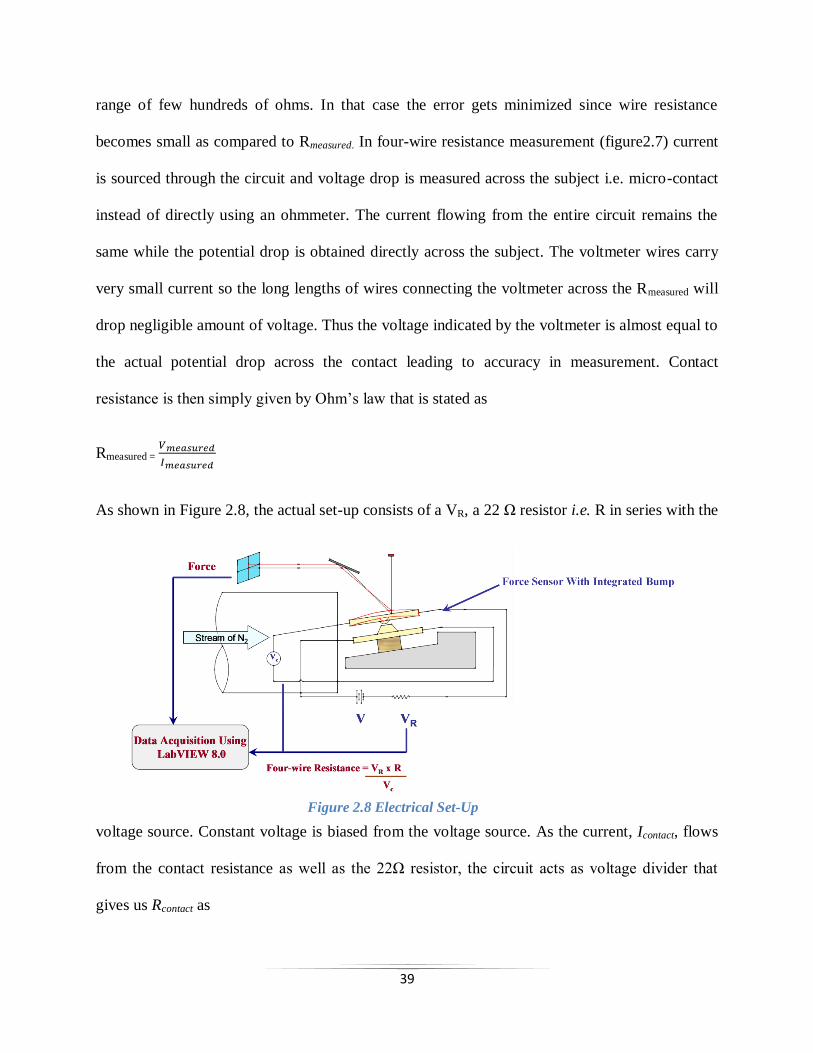
39
range of few hundreds of ohms. In that case the error gets minimized since wire resistance
becomes small as compared to Rmeasured. In four-wire resistance measurement (figure2.7) current
is sourced through the circuit and voltage drop is measured across the subject i.e. micro-contact
instead of directly using an ohmmeter. The current flowing from the entire circuit remains the
same while the potential drop is obtained directly across the subject. The voltmeter wires carry
very small current so the long lengths of wires connecting the voltmeter across the Rmeasured will
drop negligible amount of voltage. Thus the voltage indicated by the voltmeter is almost equal to
the actual potential drop across the contact leading to accuracy in measurement. Contact
resistance is then simply given by Ohm’s law that is stated as
Rmeasured =
As shown in Figure 2.8, the actual set-up consists of a VR, a 22 Ω resistor i.e. R in series with the
voltage source. Constant voltage is biased from the voltage source. As the current, Icontact, flows
from the contact resistance as well as the 22Ω resistor, the circuit acts as voltage divider that
gives us Rcontact as
Figure 2.8 Electrical Set-Up

40
Icontact = =
=
i.e. Rcontact =
Two voltage drops across the 22 Ω resistor (Vresistor) and contact resistance (Vcontact), are recorded
by the LabVIEW program. For doing the cold switching tests it is required that voltage should
biased only after the contact is made. However, if is applied continuously then it should be below
400 millivolts (4) for avoiding contact-damage due to hot switching and snap-in contact.
Set-Up for Piezo
The force sensor and pillar used during all of the experiments imitate the upper and lower portion
of an actual switch. However in our system the switching action between contact bump and pillar
is achieved with the help of piezo-electric material. We have used PL022.31 from PI. It is
attached to a stainless steel disc having a groove of 120 angle and 2mm wide with the help of
thermoplastic material STAYSTICK 442. This angle is corresponding to the default 120 angle of
the AFM tip-holder. It is done by keeping the thermoplastic in between the piezoelectric material
and the disc. The entire stack is placed on a hotplate at 1000
C. The thermoplastic melts and
piezo gets glued to the disc when it is cooled down. The pillar should always be stable on this
piezo with two connections provided on the bottom side for four-wire resistance measurement as
shown in figure 2.8. For serving this dual purpose metallic spring like structures are welded on
the custom built Alumina substrate. For electrical connections two palladium silver pads are
provided on it.

41
The piezo is actuated by the ramp function. It is loaded in first 5 milliseconds and unloaded in 5
milliseconds. When operated at 1 Hz, the remaining time is utilized in data acquisition. Agilent
function generator is used for this purpose. The signal is fed to the amplifier having gain of
~8.25. The amplified signal is then used for actuating the piezo. In addition to the function
generator, the piezo is also actuated by a DC power supply as shown in figure 2.9. This DC bias
always keeps the piezo in expanded position (figure 2.10). The amount of expansion being
dependant on the bias voltage applied, DC biasing gives added control while engaging the tip
using AFM. This voltage is especially effective while keeping the force constant. While doing
the cycling tests at higher frequencies (800Hz), the piezo experiences a small drift that reduces
the force on the beam. In this situation DC bias on the piezo is increased to keep the force
constant. It is recommended to keep it ~ 30 V at the beginning of the cycling tests however it
varies as the cycling continues depending on piezo drift. The piezo is constructed in small stacks.
When it is new, it gives full expansion of 2.2 µm at 100 V. Since the maximum range of voltage
for operating the piezo is piezo is -20V to 100 V, it is recommended that total voltage used for
expanding the piezo should be kept as low as possible for extending its life. For e.g. amplitude of
8 V from function generator and D.C bias of 20 V drives the piezo at ~86 V for achieving the
expansion of ~1.9 µm. While doing cycling tests at higher frequencies (~100Hz) such a high
Figure 2.9 Schematic Diagram Showing Piezo Set-Up
Figure 2.10 Piezo Expansion Model
42
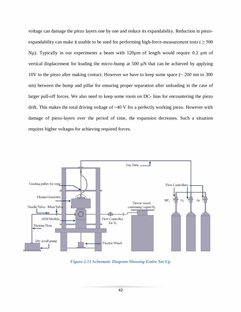
Figure 2.11 Schematic Diagram Showing Entire Set-Up
voltage can damage the piezo layers one by one and reduce its expandability. Reduction in piezo-
expandability can make it unable to be used for performing high-force-measurement tests ( ≥ 500
Nµ). Typically in our experiments a beam with 120µm of length would require 0.2 µm of
vertical displacement for loading the micro-bump at 500 µN that can be achieved by applying
10V to the piezo after making contact. However we have to keep some space (~ 200 nm to 300
nm) between the bump and pillar for ensuring proper separation after unloading in the case of
larger pull-off forces. We also need to keep some room on DC- bias for encountering the piezo
drift. This makes the total driving voltage of ~40 V for a perfectly working piezo. However with
damage of piezo-layers over the period of time, the expansion decreases. Such a situation
requires higher voltages for achieving required forces.

43
2.5 Testing Procedure
For conducting contact evolution study we require the force and resistance data across contact.
This data is not directly acquired in this set-up but in the form of three signals i.e. 1) A-B signal
from PD of AFM 2) Voltage drop across contact and 3) Voltage drop across 22 Ω resistor.
Previous section described how the two voltages and resistor interpret the contact resistance. The
A-B signal in reality gives the voltage reading on the PD depending on the laser beam deflection.
In order to convert this voltage signal into the force two types of calibrations are required.
1) Calibration of z-piezo of AFM: - The JEOL SPM has its own piezo that accurately
controls the vertical motion of the tip at nanometer level while performing scanning also
called as z-piezo. It is done by the electronics inside the AFM by regulating the voltage
on it. The Z-piezo calibration tunes the voltage needed for applying certain piezo
displacement. This is further required for doing Force vs Displacement test while doing
force calibration. Regular AFM cantilever is scanned in AC Mode across the calibration
sample 900.238 from Asylum Research having step height of 200 20 nm. Figure 2.13
shows the calibration sample and the results after scanning is shown in figure 2.12. Since,
Figure 2.12 AFM Image of the Calibration Sample
Figure 2.13 Calibration
Sample

44
the step height shown by AFM i.e 191 nm is well within the tolerance limit of the sample,
no changes in calibration scale were required.
2) Force Calibration: - This calibration actually interprets the A-B voltage signal in terms
of displacement in nanometers. While performing this, some finite displacement say
100nm is given to the regular AFM tip by executing Force vs Displacement function in
AFM. The AFM displays voltage vs displacement curve that helps us interpret the A-B
voltage in terms of displacement. It was found to be 33nm per volt which is further
multiplied by the stiffness ‘K’ of our doubly fixed beams. Thus the same A-B voltage
difference i.e. displacement can be used for applying different force by using beams of
different dimensions. It is easier to vary the length from microfabrication point of view.
So, the shorter beam can be used for conducting tests at higher forces because of their
higher stiffness and vice versa (displacement being constant). For doubly fixed beams
loaded at center, stiffness is given as (4).
K =
Where,
E = Modulus of elasticity of Si, typically 15oN/m to 180 N/m
L = Beam-length, varies from ~90 µm to 200µm
I = Area Moment of inertia of the beam
For a rectangular cross-section I =
t = Beam-thickness, typically 4µm in our case
w = Beam-width, typically ~20 µm in our case
Hence,
K = 16 E·w·

45
2.5.1 Procedure for Testing
Before starting the actual measurement of contact resistance, it is necessary to secure both the
chips of pillar and force sensor firmly on the respective holders. Since tweezers are used to hold
the Si chips and mounting them on the holders, care should be taken not to scratch them from
sideways. Even a small scratch can bring significant number of particles on the surface and pose
problems during contact engagement. For avoiding contamination problems due to skin oil it is
always recommended to wear gloves all the time during experimentation. Also, direct breathing
over the samples while mounting them on the holders is not advisable due to the contamination
issue. After setting up the sample on the corresponding holders continuity check should be
performed to see if the springs are making proper contact with the metallic layer of the samples.
Lack of proper contact of the springs to the samples can measure either no or very high contact
resistances. Perform following steps for contact resistance measurement after aforementioned
care is taken.
Steps
1) Focus laser spot on the right paddles so that there is no obstruction in laser-path.
2) Set the AFM in contact mode and reference at -1.8 V to -1.6 V. Accurately adjust PD
position so that voltage at reference is exactly -2 V.
3) Turn off laser and start the coarse adjustment by using the screw for Z+ movement.
4) Observe for the image clarity of force sensor and pillar by adjusting focal length of the
camera.
5) When the force sensor and top of the pillar are approximately at same focal length, stop
coarse movement.
6) Accurately locate center of the beam over pillar.

46
7) Turn the laser on and check PD again.
8) Click on ‘retract off’ and then ‘approach on’ to put the AFM in feedback mode while
approaching. Wait for a while until you hear a beep.
9) The beep indicates that the laser beam has moved from set position to the reference
position i.e. the bump is in contact with the pillar. Observe the laser spot deflection.
10) If it is not vertical then retract the sample and move out. Lateral movement of the laser
spot can be an indication of improper contact causing slight twisting of the beam.
11) If it is vertical (retract on and retract off and check contact-current) then apply 35 V DC
bias voltage to the piezo.
12) Go to the ‘advanced’ mode in AFM to turn off the feedback mode. Come back to contact
mode and observe the laser spot by clicking on ‘adjust PD’.
13) Reduce bias and observe the laser spot on PD. It will try to come back from the reference
position (-1.8 V to -1.6 V) to -2 V which is standard position of a freestanding tip. When
PD voltage is -2 V, apply 0.2 V across the contact and look at the current. Current should
be zero.
14) Apply waveform by using function generator.
15) Slowly increase amplitude of the waveform for increasing piezo displacement until
required ∆V is reached.
16) Acquire the data by using the LabVIEW software as soon as possible to limit the initial
data collection below 10 cycles.
17) Follow cycle-frequency table (Table 2.1) while performing cycling tests.
18) Important points to remember

47
a. Try to locate the contact accurately before coarse adjustment to avoid greater X
and Y movements
b. Constantly observe contact spots during coarse adjustment
c. Observe for the drift during feedback mode and monitor -2 V on PD
d. Try to keep pillar as close to bump as possible and avoid higher voltage on piezo
for more piezo life and reducing optical interference.
e. Constantly monitor piezo drift during cycling and increase or lower the bias
voltage or amplitude to keep ∆V constant. Do not apply more than ~8 V to piezo.
Redo the engagement and follow the same procedure again
2.5.2 Procedure for Plasma Cleaning
Clean the chamber before cleaning the first sample. We have followed the standard procedure for
cleaning the chamber i.e. 3 min of Ar plasma + 3 min of O2 plasma +3 min of Ar plasma. Initial
phase of Ar plasma cleaning is applied just to start the system. The time span of 3 min gives the
system enough time to stabilize. Also 3 min of Ar plasma treatment at the end is used in order to
remove most of the contaminants that could have formed during O2 plasma cleaning phase.
Reduction of this time span to lesser than 3 min does not make any significant changes as far as
cleaning is concerned. Follow the steps as mentioned below for plasma cleaning.
1) Turn on cooling water supply all the tanks and main power supply.
2) Check that main valve is closed and needle valve is open.
3) Start the pump.
4) Slowly open the main valve and turn off the needle valve for applying the entire pump
pressure at the vacuum chamber.

48
5) Observe for the drop in pressure indicated by pressure sensor.
6) At around 150 to 200 mTorr, turn on Ar supply at 0.3 lpm.
7) Observe for ‘Ready’ signal at plasma indicator.
8) When it’s stable at around 1750 mTorr turn on power to switch on plasma.
9) After three minutes start 0.15 lpm of O2. Wait and observe for color/brightness and
pressure change.
10) Brightness will suddenly increase when O2 plasma starts
11) Slowly ramp up the O2 supply to 0.5 lpm in the steps of 0.05 lpm
12) Wait for 3 min and then turn off O2 supply.
13) Keep Ar plasma on for 3 min.
14) Turn off the supply.
15) Turn off the main valve and open the needle valve and monitor pressure rise in the
chamber. Increase Ar flow rate to bring the chamber back to atmospheric pressure
quickly.
For sample-cleaning follow the same steps with 3 minutes of Ar followed by 10 minutes of O2
plasma cleaning
Table 2.2 is the cycle-frequency table used while doing cycling. It should be noted that the
contacts are cycled at corresponding frequencies as mentioned in table but after each cycle it is
reduced to 1Hz for data acquisition. The ‘Cycles’ column shows the total number of cycles
performed until we reach to a particular row while the figures inside the bracket ‘( )’ represents
the number of cycles that are performed in that particular step corresponding to the ‘Frequency’
and ‘Time’.

49
Table 2.1: - Cycle-Frequency Table

50
Chapter 3- Simulation
3.1 Simulation of Pure Au-Au Contact
According to the formula given by Holm (26), the constriction resistance is given by
RH =
(1)
where ρ is the resistivity of the contacting metals and ‘a’ is the radius of circular contacting spot.
This formula holds good for the contact-spots connecting semi-infinite bodies. In MEMS
switches surfaces are often coated with the films having varying thicknesses (from ~10nm to
~1µm). As a contact-bump starts making contact with its counterpart, the nano-asperities present
on the films start getting pressed against each other. Increase of force brings more and more
asperities into contact resulting in increase of effective contact area. The total contact area is,
thus, few hundred times smaller than the contact bump or bottom part. In cases, when the contact
area is no longer small as compared to the thickness of the film, application of equation (1) for
estimating constriction resistance by Holm's theory can consist of some errors. It is called as
distorted constriction (9). The contact resistance is no longer dominated by the Holm constriction
at the contact. In this case we need to include the spreading resistance from the contact area into
the thin film.
According to the simulation performed by Eid (27), the radius of Au-contact, ‘a’, is ~0.34µm
with the film thickness of 300 nm when the contact is loaded at 500 µN. The force sensor is ~20
µm wide and ~80 µm long. In this case ‘a’ becomes comparable to the film thickness and contact
resistance predicted by Holm is 0.0717 Ω if we consider ρ = 2.44 µΩ-cm for Au (28). Most of

51
the measured values have always remained considerably higher (~0.15 Ω to ~0.18 Ω) than
predicted by the theory.
The simulation for pure Au-contact is conducted to understand the trend of resistance when the
thickness of the film is varied. This simulation also helped us in closely predicting the contact
resistance values for particular metallization stack when loaded at particular force. The
simulation mentioned in the next sections of this chapter were performed by me under the
supervision of Dr. Chen.
For conducting the simulation electric
module Ansys 11.0 is used. For
performing current conduction analysis
‘SOLID 98’ element is selected. It is a
tetrahedral element with 10 nodes. It can
take 6 degrees of freedom. According to Ansys reference manual, (29) for conducting steady
state current conduction analysis only current and voltage DOF are applied and the output is
given in the form of current density and voltage distribution. Ansys sparse solver which is the
default solver is used for conducting the simulations.
Figure 3.1 Schematic Diagram of the Model of Simple
Metal-Metal Contact

52
In first model the contact radius is kept constant at 0.5 µm and two block of 40µm x 40µm are
connected to each other only at this contact area as shown in figure 3.2 and the third dimension
i.e. thickness is varied. Since the entire testing is done by conducting four-wire resistance
measurements, similar conditions are taken while doing simulations as well. Voltages of 0.2V
and 0 V are applied at the corresponding areas as shown in figure 3.1. All the other areas
including the area surrounding the contact area are insulated. For this simulation bulk resistivity
of Au is taken as ρ = 2.44µΩ-cm (28) and
the height of the contact area is zero. This
voltage difference drives the current
through the contact area as shown by the
blue arrow in figure 3.1. Both these
volumes are meshed at fine level (Fine 1)
by using Ansys smart meshing tool and
type of elements used is tetrahedral. For
improving the accuracy of the results the
areas near the contact-area are refined at the
level of refinement of 1 as represented in figure 3.2. Thickness of the two blocks is decreased
from 40µm to 0.1 µm in 9 steps. Decrease in thickness from 40µm to 100nm causes a large
change is aspect ratio. This variation also causes a large increase in the total number of elements
formed in the model after meshing. In every step the voltage drops on the opposite areas are
observed as they are measured as V1 and V2 respectively. (V1 – V2) gives the total voltage drop
across the contact. Current flowing through the contact area is same as the one flowing from the
area where 0.2 V is applied. Current density recorded by the Ansys postprocessor is multiplied
Figure 3.2 Meshing of Two 40µx40µx40µ Blocks
in Contact With Each Other By Contact Area
Having a = 0.5µm Radius

53
by this area to get current flowing from contact. Contact resistance, R, is then calculated by using
Ohm’s law.
R =
(2)
Figure 3.3 illustrates the simulation results of this model. Ansys simulation results agree well
with the Holm’s model when the thicknesses of blocks are larger as compared to the contact-
diameter. However as when the block-thickness becomes comparable to the contact-diameter,
the simulated resistance remains no longer consistent with Holm’s theory. So, a 300 nm thick
Au-Au contact having 0.5 µm contact radius would have the four-wire resistance in the range of
0.8 Ω instead of 0.024 Ω as predicted by Holm’s theory.
Figure 3.3 Simulation Results Showing Resistance vs Thickness Plot

54
The simulation is further pursued by
modeling the real structures coated with 300
nm of Au and Ru respectively. Contact radii
are taken from the simulation performed by
(27). Since most of the metal-contact pairs
are tested at either 100 µN or 500 µN during
the experiments, simulations are conducted
by modeling the contact-radii at corresponding forces (Table 3.1) for corresponding metals. The
models are created in Pro/ENGINEER WILDFIRE 4.0. Figure 3.4 shows an example of voltage
distribution for Au-Au contact loaded at 500µN. Resistivity of 300nm film was measured as 3.6
µΩ-cm for Au and 13.8 µΩ-cm for Ru. The force sensor modeled here is 15 µm x 80 µm and 4
µm thick. It has a contact bump having radius of curvature of 20µm and 1µm height. The pillar is
having trapezoidal shape with the bottom-square of 40µm and top-square of 20µm. Height of the
pillar is taken as 20µm and the substrate is 100µm X 100µm. Table 3.1 given below gives
contact resistances for these structures at respective forces and compares it with the values
estimated by equation (1) and experimentally measured data. Experimentally measured values
show close resemblance with the values predicted by Ansys models especially at 500 µN. This
can be because of the involvement of spreading resistance at higher forces due to higher contact
radii. Another reason behind this close agreement between measured values and Ansys-predicted
values can be due to the sheet resistance of thin metallic films on the pillar walls.
Figure 3.4 Simulated Voltage-Distribution for
the Model With Real Geometry

55
3.2 Simulation of Layered Ru
Layered Ru is a new kind of contact-metal that is studied during experimentation. This
comprises of Ru-layers having thicknesses of 10 nm, 50 nm, 100 nm, 300 nm deposited over 300
nm layer of Au respectively over the
Si force sensor. The pillars are initially
electroplated with Au having the
thickness of 500 nm for avoiding the
sheet resistance effect arising from
pillar-walls. It is further sputter-coated
with 300 nm of Au layer. Hence, the total Au thickness for pillar becomes 800 nm. The
advantage of using Au layer beneath the Ru is that the lower resistivity of Au allows most of the
current to pass through the Au layer when the Ru-Ru contact is made. It is further explained in
detail in Chapter 4.
The model used here is quite similar to the one used in previous section however it consists of
two layers on one side of the contact as shown in figure 3.5. The thickness of Au layer is fixed at
Table 3.1 Simulated Contact Resistances for the Model With Real Geometry
Figure 3.5 Schematic Diagram of the Model Having
Layered Structure

56
500 nm for simulation while the Ru-layer thickness varies in each set. The contact-radii at
different forces where Ru-layer from one component meets the Ru-layer of the other is selected
from (27). Total four sets of Ru thicknesses i.e.10nm, 50 nm, 100 nm, 300 nm over 500 nm of
Au are simulated. Figure 3.6 shows the increase in contact-radius with the increase in applied
force. All the parameters used in this simulation are similar those in previous section. Bulk
resistivity of Au is taken as 3.6 µΩ-cm from experimentally measured data. Table 3.2 gives the
resistivity values of Ru films. These values are measured experimentally and used for doing
simulations.
No. Thickness (nm) Resistivity (µΩ-cm)
1 300 14.82
2 100 21.34
3 50 25.89
4 10 36.4
Table 3.2 Measured Resistivity Values for Different Thicknesses
In this case, the total contact resistance is
approximated as the sum of constriction
resistance Rc and film resistance Rf (9) It is
represented as
RCR = Rc + Rf =
+
Where ρ’ is the resistivity of Ru film and ρ is the
resistivity of the bulk material which is Au in our
case.
Figure 3.6 Simulated Contact Radius vs
Force by Eid(27)

57
Since the thickness of 50 nm and 10 nm Ru films becomes comparable to the mean free path of
electrons flowing from Au and Ru layers, Sharvin resistance has to be taken into consideration.
The electrons flowing across the cross-section also suffers extra resistance at the boundary
separating two metals called as boundary scattering.
If the constriction resistance is accurately calculated by considering the both these effects into
account then RCR can be given as
Rc =
RM +Rs =
.
+
RCR =
RM +Rs =
.
+
+ Rf (3)
Where RM is the Maxwell spreading resistance due to lattice scattering and Rs is the Sharvin
resistance due to the boundary scattering (9). Furthermore ρ is the electrical resistivity of Ru, γ is
the interpolation function and λ is the mean free path of electrons i.e. 10.8nm for Ru and 38nm
for Au.
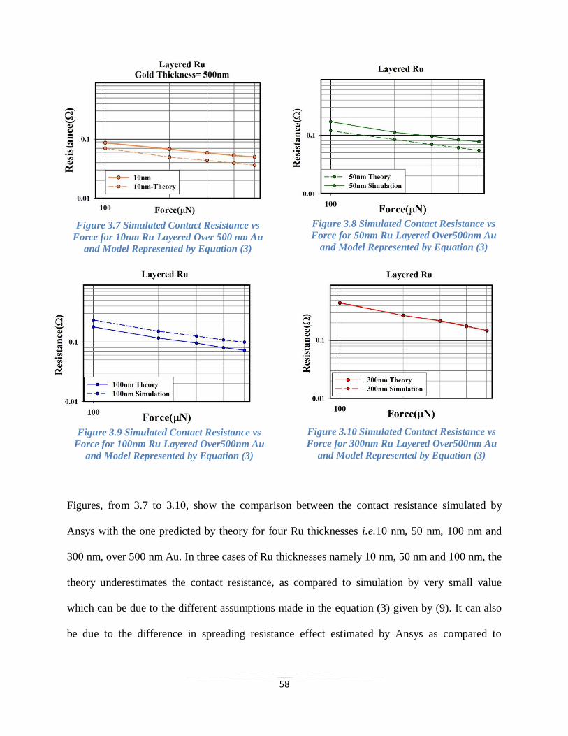
58
Figures, from 3.7 to 3.10, show the comparison between the contact resistance simulated by
Ansys with the one predicted by theory for four Ru thicknesses i.e.10 nm, 50 nm, 100 nm and
300 nm, over 500 nm Au. In three cases of Ru thicknesses namely 10 nm, 50 nm and 100 nm, the
theory underestimates the contact resistance, as compared to simulation by very small value
which can be due to the different assumptions made in the equation (3) given by (9). It can also
be due to the difference in spreading resistance effect estimated by Ansys as compared to
Figure 3.8 Simulated Contact Resistance vs
Force for 50nm Ru Layered Over500nm Au
and Model Represented by Equation (3)
Figure 3.7 Simulated Contact Resistance vs
Force for 10nm Ru Layered Over 500 nm Au
and Model Represented by Equation (3)
Figure 3.9 Simulated Contact Resistance vs
Force for 100nm Ru Layered Over500nm Au
and Model Represented by Equation (3)
Figure 3.10 Simulated Contact Resistance vs
Force for 300nm Ru Layered Over500nm Au
and Model Represented by Equation (3)

59
equation (3). For 300nm layered Ru case, the model given by equation (3) seems to agree well
with the Ansys model. This can be due to the contribution of resistances from thick Ru films. At
300 nm Ru films have smaller contact radii as compared to the Ru thickness especially in low
force regime (<500 µN) . In this case Ru can behave like bulk material instead of a film.

60
Chapter4- Discussion of Data and Results
4.1 Au_Au: -
We started our experiments with Au on both sides of the contact. As we have seen in Chapter 1
that Au is a popular metal in MEMS contact switches, several attempts have been made to test it
in different conditions. As we will see in next section, most of the research groups have reported
stiction problems. Gold, with its lowest resistivity among the contact-metals used in MEMS
industry and noble nature, can give us the reference line for testing other metals. With the results
obtained after testing Au-contact under various conditions of applied load and cleaning, different
contact-metals were compared with Au quantitatively for their contact resistance and stiction.
The metal-pairs that can exhibit contact resistances closer to Au-contacts but lower adherence
force until ~108 cycles can be termed as an electromechanically sound metal-contact pair. In our
experimentation, because of the manual data acquisition method, contacts were tested until 106
or 107 cycles. The data acquired helps us understand the trends revealed by different metal-pairs
under different conditions and compare them in order to find a better substitute for Au-contacts.
The experiments were conducted in two stages to understand the trends of electrical and
mechanical curves during cycling tests.
Stage One:- Four-wire resistance measurement in open ambient
Stage Two:- In-situ and ex-situ cleaning of the metal-contacts under different plasmas
and UV/Ozone followed by cycling

61
Stage One: - Stage one was very critical to understand the basic nature of A-B curves in
different phases of contact-evolution for different metals. Figure 4.1 represents the most common
A-B data-plot acquired after ~10cycles for an Au-Au contact loaded at 100µN from our system
by using LABVIEW.
The most important steps while performing
loading and unloading are represented by in
orange color with numbers. At point 1, the
piezo starts expanding in response to the
waveform applied. From point 1 to point 2
piezo keeps on expanding due to a very small
gap between the contacts. The bump does not
come in contact with the pillar until point 2.
At this point, pillar mounted on piezo starts
pushing the contact bump on the force sensor. The fixed-fixed beam structure thus bends in
upward direction. This linear deflection is also associated with rotation, as explained in Chapter
2, making the laser beam deflect. Figure 4.1 shows the calibrated A-B signal. The beam further
bends until it reaches point 3. Point 3 is the state of maximum piezo-expansion with respect to its
driving voltage. In the mean while, the electric current flows from the contact when the contact is
made at point 2 resulting in sudden resistance drop. Thus, from point 2 to point 3 completes one
loading curve of one cycle. As we have applied a ramp signal for loading and unloading, piezo
retraction starts from point 3. Loading force applied on the beam and hence the deflection
decreases to move the laser spot downwards. It finally returns to its reference position. This is
called as an unloading curve.
Figure 4.1 Sample Signal Acquired from AFM
62
Ideally, the process of unloading should end here with point 4 lying at 0µN force. However, if
metal surfaces, especially Au, are very clean then the film on the pillar gets stuck to the film that
is coated on micro-bump due to the force of adhesion. The bonds developed during this process
are very weak. However at micro-meter level the pull-off force is quite dominant over other
forces. Therefore, the pillar starts pulling down the beam further and laser spot begins to deflect
in negative direction. Contact between metallic counter-parts keeps the current flowing from
circuit. Pillar keeps on going down while piezo is restoring and the beam bend further. This
process continues until the bump experiences maximum pull from pillar. Just after this point i.e.
point 4, weak bonds between the two suddenly break and the beam pops back to its original
shape. Laser spot, accordingly, goes back to the reference position at point 5. Current flowing
through the contact now stops as the two parts get isolated. From point 3 to 5, comprises of
unloading phase of one cycle. Piezo further retracts until it comes back to its original shape i.e.
point 6 in figure 4.1 when biased voltage gets zero. This entire process makes one complete
cycle of switch-contact. If the contacts are not damaged due to yielding or material transfer then
its separation after pull-off happens so quickly that, on the time scale, the A-B signal is acquired
as a vertical line joining points 4 and 5. Hence, point 5 stands for maximum pull-off force
recorded. Figure 4.1 is representing the same behavior with maximum pull-off force of 67.8µN.
Pull-off forces in the range of 100 µN are normally considered as too high from switch-designing
point of view.
For Au contacts, pull-off forces have been reported in the range of 20 µN for the applied forces
of around 50 µN (30). Also a gradual increase in pull-off force up to 400 µN has been reported
by Gilbert (31) with the applied force in the range of 1mN when the Au switch-structure was
cycled until 60,000 cycles under hot switching conditions. Efforts have also been made to report

63
the change in resistance for Au. Contact resistance reported by (8) is around 0.4 Ω with the
applied force of 200 µN while (14) ~0.2 Ω to 0.3 Ω with the applied load of 150 µN. Kwon et al
(11) were successful in measuring low resistance data however the load applied to achieve that
was 50mN which is so high that is well beyond the practical consideration 100uN to 1mN.
Dickrell et al(17) have made good attempt to measure the resistance and pull-off force
simultaneously. Their test structure reports contact resistance of 930 mΩ at 150 µN with the pull
off force of 45 µN. All of the test set-ups mentioned here have used hot-switching conditions
with 0.1 A as sourced current. With a novel switch experiments performed at MIT, Kim (10) has
recorded 0.1Ω resistance at 150 µN until 1010
cycles. The purpose of the test-set-up built here in
NEU is to test different material pairs under different forces after proper cleaning of the micro-
contact. Following sections discuss the results of different tests performed on Au-contact. For
convenience, the metal that is coated on the force sensor is stated first while the one on pillar
side comes second separated by hyphen. For example Au-Ru means that gold is coated on force
sensor while ruthenium is coated on pillar side.
Stage One: -
Figure 4.2 Au-Au Contact Resistance at
Different Forces After ~10 cycles
Figure 4.3 Au-Au Contact Resistance When Cycled
at Particular Forces as Shown by the Bold Dots

64
This was the very first stage of the experimentation. In this stage Au-Au was tested under
different loading forces in open ambient without doing plasma cleaning or UV/ Ozone cleaning.
Freshly coated samples were used for conducting these tests without using N2 ambient control.
Since Au is resistant to most of the air-borne contaminants, strategy of using freshly coated
samples was good enough to conduct the required measurements. The data shown in figure 4.2 is
acquired by Dr. Chen before the contact underwent 10 cycles at particular force. As shown in
figure 4.2 a typical Au contact exhibits contact resistance of around 0.2 Ω when loaded at 100
µN initially. Holm’s theory states that the contact resistance decreases with the increase in
contact area. This is clearly validated from the measurement-data shown in figure 4.2. Initially
when 100 µN are applied on the contact, only a few asperities contact each other. The effective
contact radius of ~0.2µm (27) causes the contact resistance of ~0.2 Ω. Repetitive switching
(cycling) and application of higher force are the two modes of bringing more and more asperities
into contact and increasing effective contact-radius. Both of these processes lessen the contact
resistance in exponential manner. Figure 4.2 clearly shows the effect of application of higher
force on contact resistance as well as pull-off force. Contact resistance decreases from ~0.2 Ω at
100 µN to ~0.13 Ω when loaded at 500 µN. At the same time, with increase in contact area, pull-
off force increases in same proportion. Au contacts typically demonstrate the pull-off force in the
range of 60 to 70µN with the application of 100 µN, at the beginning of cycling. Gold being very
soft, the rate of increase of contact area is much higher for pure Au-Au contact than any other
metal-pair. Hence, the adherence force increases very rapidly as the applied force increases. It is
~500µN for the Au-Au contact loaded at 500µN.

65
Figure 4.3 gives a wider picture of the decrease in resistance when contact is cycled at 100 µN.
As shown in figure 4.3, the Au-Au contact resistance has shown decrease from ~0.24 Ω to
~0.18Ω for the contact cycled at 50µN and from ~0.2Ω to ~0.16Ω when the contact is cycled at
100µN. It also illustrates that, as the loading force increases, the amount of decrease in contact
resistance due to cycling decreases. In short cycling the contact until 106 cycles at 50µN would
exhibit significant decrease in contact resistance due to cycling. However if the same contact is
cycled at 500µN, the decrease in contact resistance would not be significant enough. This is due
to the same reason as explained in previous section. The force of 500µN is so high for an Au-
contact that it brings most of the asperities into contact even at the early stages of contact-
evolution. Cycling of such a contact until 106 does not make significant for the contact
resistance. However contacts can fail to separate due to high stiction.
Stage Two: -
After understanding the general behavior of Au-Au contacts under different forces, the focus was
given on performing plasma treatment on Au contacts. The purpose of this stage was to
understand the effects of argon, oxygen, nitrogen and NF3 plasma and UV/Ozone on Au and then
to determine the appropriate treatment to clean the metal surfaces.
In-situ Plasma Cleaning Tests:-
The experiments were started in order to understand the in-situ plasma cleaning effects on Au-
Au contact. The force sensor and pillar coated with Au were engaged by using AFM as
explained in Chapter 3. Ar plasma at 0.3 lpm and 1750 mTorr was introduced while the contacts
were switching at 100 µN at 1 Hz throughout the testing. Ar plasma was operative for 5 minutes.
Contact-data was acquired at the interval of 1 min. After 5mins of Ar plasma, O2 gas was

66
introduced into the chamber at 0.5 lpm to initiate the treatment under O2 plasma.O2 plasma was
turned operated for 15 minutes and measurement was done at the interval of 1 min. After 15 min,
O2 gas was turned off and contacts were again treated under 5 minutes of Ar plasma for
observing the changes in contact resistance and pull-off force. Thus in-situ cleaning had three
stages: - 5minutes Ar plasma - 10minutes O2 plasma - 5minutes Ar plasma.
Figure 4.4 shows the changes in contact resistance and pull-off force for an Au-Au contact
during three stages of in-situ plasma treatment. Ar plasma did not show any significant effect on
pull-off force and resistance almost remained unchanged for 5min. However, as soon as the O2
was introduced sudden drop in pull-off force was observed while resistance increased gradually
over the period of 15mins. This can be due to the presence of thin oxide film on Au surface (32).
Figure 4.5 reveals the rise in contact resistance from ~0.4Ω to ~1Ω after 15min of in-situ O2
plasma cleaning. In these trials, the force sensor and bump were not exposed directly to the
downstream plasma. This can reduce the effect of O2 plasma treatment. Also, the plastic used
inside AFM (as the part of tip-holder) and thermoplastic that is used to fix the piezo to the disc
Figure 4.4 In-situ Plasma Cleaning Experiment
on Au-Au Contact
Figure 4.5 Resistance Vs Force Diagram
Showing Effect of In-situ15 min In-situ O2
Plasma on Au-Au Contact

67
might not be good. The active oxygen species present in O2 plasma can react with the plastic to
produce unwanted gasses and contaminants such as CO, CO2 near the contact.
In-situ tests provided us with some understanding of the behavior of Au contact under Ar and O2
plasma. In order to eliminate the possible sources of contamination in the in-situ tests, samples
were cleaned by separately placing the plasma-chamber on a thick glass slab. This method was
relatively simple and quick as compared to in-situ tests.
Ex-situ Plasma Cleaning: -
In these tests the chamber was placed separately on a glass slab. Samples were directly placed on
the glass slab facing upwards such that the downstream plasma would directly bombard on the
metallic layer. In this situation, only the samples remain inside. Hence all the probable factors
such as thermoplastic from the holder, connecting wires, plastic from tip holder etc. that can
cause the contamination are eliminated. Samples are directly exposed to the plasma stream
instead of sideways like it was during in-situ plasma cleaning. All the experiments conducted
under constant stream of N2.

68
Since Ar plasma displayed its inefficiency during in-situ plasma cleaning, focus was given on
observing effects of O2 plasma on Au-contact. For initial trials, samples were treated under 3min
of Ar plasma followed by 10 min of O2 plasma. The cleaning was initiated with Ar plasma
because that is requirement for switching on the plasma generator. The time interval of 3 min for
Ar plasma was chosen arbitrarily. It gives the system enough time to stabilize. However it should
be noted that this time i.e. 3 min is not very crucial for removing contamination when the
cleaning are further going to be cleaned under 10 min of O2 plasma treatment. Hence reduction
of this time period does make any significant changes in contact resistances (after O2 treatment).
3 min of Ar plasma treatment can be helpful only for removing the contaminants that are loosely
bonded on the surface as explained in Chapter 1. After 3 min of Ar plasma, O2 gas should be
immediately turned on as explained in previous section. The pressures and gas flows were
maintained at same levels as that were during in-situ plasma cleaning. It is important to note that
the samples should be engaged as quickly as possible after treatment to avoid their exposure to
moisture and other gasses in environment.
Figure 4.6 Au-Au Cleaning Effect of O2
Plasma Cleaning on Pull-off Force
Figure 4.7 Au-Au Cleaning Effect of O2
Plasma Cleaning on Contact Resistance
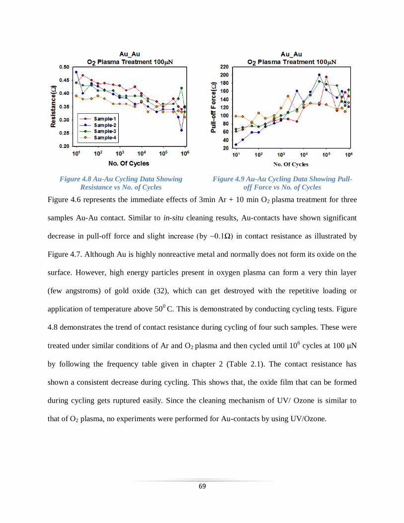
69
Figure 4.6 represents the immediate effects of 3min Ar + 10 min O2 plasma treatment for three
samples Au-Au contact. Similar to in-situ cleaning results, Au-contacts have shown significant
decrease in pull-off force and slight increase (by ~0.1Ω) in contact resistance as illustrated by
Figure 4.7. Although Au is highly nonreactive metal and normally does not form its oxide on the
surface. However, high energy particles present in oxygen plasma can form a very thin layer
(few angstroms) of gold oxide (32), which can get destroyed with the repetitive loading or
application of temperature above 500
C. This is demonstrated by conducting cycling tests. Figure
4.8 demonstrates the trend of contact resistance during cycling of four such samples. These were
treated under similar conditions of Ar and O2 plasma and then cycled until 106 cycles at 100 N
by following the frequency table given in chapter 2 (Table 2.1). The contact resistance has
shown a consistent decrease during cycling. This shows that, the oxide film that can be formed
during cycling gets ruptured easily. Since the cleaning mechanism of UV/ Ozone is similar to
that of O2 plasma, no experiments were performed for Au-contacts by using UV/Ozone.
Figure 4.8 Au-Au Cycling Data Showing
Resistance vs No. of Cycles
Figure 4.9 Au-Au Cycling Data Showing Pull-
off Force vs No. of Cycles

70
This can also be revealed by figure 4.9 which shows significant rise
in pull-off force for Au-Au contact, especially after 103 cycles. At 10
5
pull-off forces are even in the range of ~200µN which is extremely
unfavorable for the contact-switches. It should be noted that
alignment of the force sensor and bump exactly at 120 is very critical.
Slight misalignment can produce sliding of the micro-contacts while
switching as shown in SEM image (figure 4.10) taken by Dr. Chen.
This can lead to even higher pull-off forces due the damage of the surface film.
Types of Failures Observed in Au-Au Contact During Cycling Tests: -
High adherence force causes significant increase in pull-off force. Figure 4.11 shows one such
example where an Au contact is cycled at 100 µN until 106 cycles. During switching the pull-off
forces were increased more than 3 times the applied load and made contact-separation difficult.
Figure 4.12 illustrates a contact-failure due to ductile separation. In this case also Au contacts
were cycled at 100 µN until 106
cycles. Pull-off force displayed abrupt variation during cycling
Figure 4.11 Au-Au Contact Showing High Pull-
off Force During Cycling
Figure 4.12 Au-Au Contact Ductile Separation
Figure 4.10 Sliding
Occurring at Au-Au
Contact Due to
Misalignment
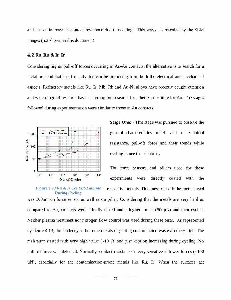
71
and causes increase in contact resistance due to necking. This was also revealed by the SEM
images (not shown in this document).
4.2 Ru_Ru & Ir_Ir
Considering higher pull-off forces occurring in Au-Au contacts, the alternative is to search for a
metal or combination of metals that can be promising from both the electrical and mechanical
aspects. Refractory metals like Ru, Ir, Mb, Rh and Au-Ni alloys have recently caught attention
and wide range of research has been going on to search for a better substitute for Au. The stages
followed during experimentation were similar to those in Au contacts.
Stage One: - This stage was pursued to observe the
general characteristics for Ru and Ir i.e. initial
resistance, pull-off force and their trends while
cycling hence the reliability.
The force sensors and pillars used for these
experiments were directly coated with the
respective metals. Thickness of both the metals used
was 300nm on force sensor as well as on pillar. Considering that the metals are very hard as
compared to Au, contacts were initially tested under higher forces (500µN) and then cycled.
Neither plasma treatment nor nitrogen flow control was used during these tests. As represented
by figure 4.13, the tendency of both the metals of getting contaminated was extremely high. The
resistance started with very high value (~10 Ω) and just kept on increasing during cycling. No
pull-off force was detected. Normally, contact resistance is very sensitive at lower forces (~100
µN), especially for the contamination-prone metals like Ru, Ir. When the surfaces get
Figure 4.13 Ru & Ir Contact-Failures
During Cycling
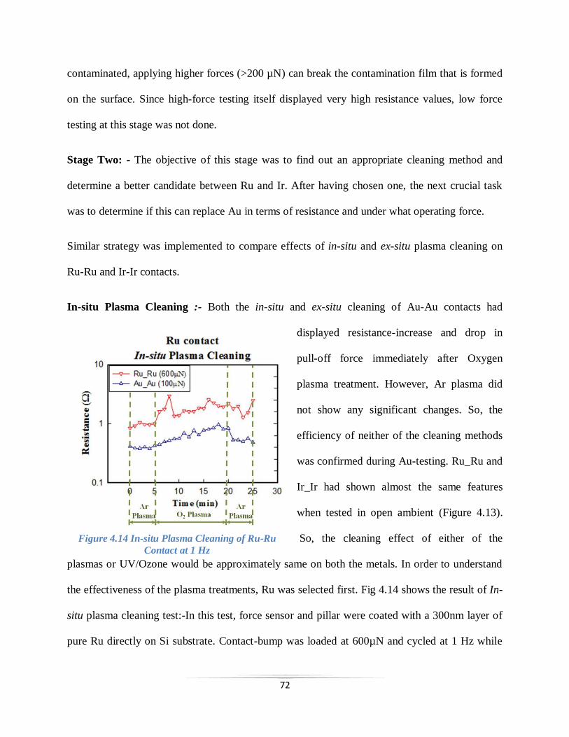
72
contaminated, applying higher forces (>200 µN) can break the contamination film that is formed
on the surface. Since high-force testing itself displayed very high resistance values, low force
testing at this stage was not done.
Stage Two: - The objective of this stage was to find out an appropriate cleaning method and
determine a better candidate between Ru and Ir. After having chosen one, the next crucial task
was to determine if this can replace Au in terms of resistance and under what operating force.
Similar strategy was implemented to compare effects of in-situ and ex-situ plasma cleaning on
Ru-Ru and Ir-Ir contacts.
In-situ Plasma Cleaning :- Both the in-situ and ex-situ cleaning of Au-Au contacts had
displayed resistance-increase and drop in
pull-off force immediately after Oxygen
plasma treatment. However, Ar plasma did
not show any significant changes. So, the
efficiency of neither of the cleaning methods
was confirmed during Au-testing. Ru_Ru and
Ir_Ir had shown almost the same features
when tested in open ambient (Figure 4.13).
So, the cleaning effect of either of the
plasmas or UV/Ozone would be approximately same on both the metals. In order to understand
the effectiveness of the plasma treatments, Ru was selected first. Fig 4.14 shows the result of In-
situ plasma cleaning test:-In this test, force sensor and pillar were coated with a 300nm layer of
pure Ru directly on Si substrate. Contact-bump was loaded at 600µN and cycled at 1 Hz while
Figure 4.14 In-situ Plasma Cleaning of Ru-Ru
Contact at 1 Hz

73
the plasma treatment is going on. The trial was conducted in three stages 1) 5 min of Ar plasma
cleaning 2) 15 min of O2 plasma cleaning 3) 5 min of Ar plasma cleaning and the data was
acquired at the intervals of 1min in similar manner as explained in previous section. 5min of Ar
plasma did not show any change in contact resistance for Ru-contact. However it displayed
immediate rise when O2 plasma was introduced and remained higher (>1Ω) until O2 plasma was
on. Contact resistance decreased slightly when O2 plasma was turned off after 15 min. In short,
the in-situ plasma treatment for Ru also failed to bring down the contact resistance and similar to
Au slight increase in contact resistance was observed. The pull-off forces observed during the
tests on Ru-Ru or Ir-Ir were extremely low (≤ 5µN). The inefficiency of in-situ plasma treatment
can be because of the similar reasons given for in-situ cleaning of Au contacts.
Ex-situ Plasma Cleaning: - Ru samples were treated with both the plasmas (Ar and O2)
separately for different durations. These trials showed very clear decrease in contact resistance
even for very dirty samples having initial resistance above 50 Ω before cleaning. All these tests
were carried out by placing the vacuum chamber separately on a glass slab as explained in
previous section. All the measurements were obtained under the constant stream of nitrogen.
Ar Plasma Treatment: -
Ar plasma treatment, in our set-up, can involve cleaning due by the heating due to the action of
radicals and electrons that can only remove some of the loosely bonded contaminant particles
and moisture. Ar plasma itself showed some remarkable cleaning result on Ru samples.
Resistance can be further brought down by increasing the treatment duration. Figure 4.15
illustrates the effects of Ar plasma cleaning on Ru-contact. It also clear that time of treatment
makes significant difference in reducing contamination. However Ar plasma, due to the lack to
chemical reactions, has limitations on its efficiency. Even small traces of contaminating

74
molecules such as polymers, hydrocarbons etc. if remained on the contacting surfaces can be
harmful. During switching with the current flowing across the contact, these molecules can build
a contamination film which can again increase the resistance making the cleaning ineffective.
Figure 4.16 illustrates one such example of a cleaner Ru contact after 10 min of Ar plasma
treatment but while cycling, the contact again got contaminated and resistance rose very quickly.
In this case, even the application of 500 µN was insufficient to break the contamination films
those were formed on the surface during cycling.
Figure 4.15 Ex-situ Ar Plasma Cleaning Effect
on Ru-Ru Contact Resistance
Figure 4.16 Ru Contact Cycled at 500 µN
After Ar Plasma Treatment

75
O2 Plasma Treatment:-
O2 plasma, unlike Ar plasma, because of its
dual cleaning action i.e. knock-out of the
contaminants and oxidation reactions, becomes
more effective as compared to Ar plasma.
Figure 4.17 gives us an idea about the
efficiency of O2 plasma cleaning. It should be
noted that all the contacts were first treated
under 3min of Ar plasma before actuating O2
plasma. Even two minutes of treatment was able
bring down the contamination-level significantly. It is important to note that the applied forces
were 100µN in this case. O2 plasma treatment followed for 10 minutes and 20 minutes showed
remarkable difference in the cleaning-efficiency as compared to Ar plasma-cleaning. A few trial
were also taken with 20min of O2 plasma but it did not prove to be significantly effective than 10
minutes shown in figure 4.17. Figure 4.18 shows an example of substantial decrease in contact
resistance after ex-situ cleaning for 3 min of Ar + 10 minutes of O2 plasma treatment on Ru
contact loaded at 100 µN. Normally when a contact is loaded, the contact resistance decreases
with the increase in load due to the increase in contact area. So, when the contact is unloaded
from the same force, the contact resistance should follow the same path as it was during loading.
However in our set-up we have typically observed a slight decrease in contact resistance during
unloading phase especially for the contacts before cleaning as shown in figure 4.18. The exact
reasons behind this phenomenon are unknown. However it is speculated that the minor errors
during micro-fabrication can make the force sensor (and hence the contact-bump) asymmetric
Figure 4.17 Ex-situ O2 Plasma Cleaning Effect
on Ru-Ru Contact Resistance

76
about the center. This can lead to slight rolling of the micro-contacts during unloading phase.
The effects can be more prominent if a thin contaminant-film is present on the surface leading to
decrease in contact resistance while unloading.
Resistances were measured consistently ~1Ω when contacts were loaded at 100µN and ~0.8 Ω
under the loading of 500 µN after cleaning (figure 4.19). As a common trend of a Ru-Ru contact
during cycling (after 10min O2 cleaning), a sharp rise in resistance until 103 cycles was observed
followed by a sudden drop and then steady descent in resistance as the typical trend for Ru
contacts. Fig 4.19 illustrates the same phenomena for two tips loaded at 100µN and 500µN
respectively. We never observed any pull-off force for Ru-Ru and Ir-Ir contacts.
UV/Ozone involves similar oxidation reactions. However it was not as effective as O2 plasma as
illustrated by figure 4.20 that gives quick review of three methods. For making UV/Ozone
cleaning more effective, distance of the samples from source, pressure conditions and Oxygen
flow should be maintained very accurately (22). Figure 4.20 indicates the comparison of three
4.19 Cycling Data of Ru-contact After O2
Plasma Treatment
Figure 4.18 Cleaning Effect of O2 Plasma
on Ru-Ru at 100µN

77
cleaning methods carried for 10 min
when Ru-Ru contacts are tested at
100µN. Close distribution of contact
resistances ~1Ω after 10 min of O2
plasma treatment clearly displays its
over UV/Ozone and Ar plasma
cleaning.
Finally it was concluded that, for our
system, the treatment of 3 minutes of Ar plasma followed by 10 min of O2 plasma was sufficient
enough to clean the surfaces after proper handling of samples during fabrication. It is worth to
note that, if the resistance vs. force curve after cleaning does not look nice and flat as shown in
figure 4.18, one should follow one more cycle of 3min of Ar plasma and 10 min of oxygen
plasma treatment.
After the successful trials of O2 plasma on Ru-
contacts, the same strategy and methods were
applied on Ir-contacts. O2 plasma was able to
bring down the Ir contact resistance below 1Ω.
However it did not sustain for many number of
cycles. Ir-Ir contacts have displayed rapid
contamination- failure. Figure 4.21 shows one
such example of Ir contact that was treated for
3 min of Ar + 10 min of O2 plasma treatment.
Figure 4.21 Cycling Data of Ir Contact After O2
Plasma Treatment
Figure 4.20 Comparison of Three Cleaning Methods

78
Even, the application of 600µN failed to provide stable contact resistance and displayed quick
rise after only 104 cycles when tested under N2 ambient control.
Our second stage was finished here with the conclusion that 3min of Ar + 10 min O2 plasma
treatment was better than Ar plasma and UV/Ozone cleaning. It also confirmed that Ru-Ru
contact are reliable than Ir-Ir contacts even at low forces (100µN). Although Ru-Ru did not
display any stiction as that in Au-Au, resistances recorded were much higher than Au. This can
be a limiting factor in its usage as a contact metal in MEMS switches.
4.3 Au_Ru & Au_Ir
As explained in previous section, using only Ru or Ir on both sides for contact did not provide
any promising results from reliability point of view. Ru showed some features that proved it
superior than Ir to some extent. However if one is looking for a better substitute for Au for
MEMS applications then lower resistances (~0.2 Ω to 0.3 Ω) at lower forces (~100 µN to 150
µN) should be achieved. The metal-pair should exhibit lesser adherence. While using a
combination of two metals, it is critical to decide their locations. Two factors were considered
while taking the decision. Ru, when deposited on beams develops residual stress (33). This stress
causes the beam to buckle in upward direction. Controlling pressure during Ru-deposition for
fabricating stress-free unbuckled beam was found to be very tough. Similar was the case for Ir
deposition but the buckling was in opposite direction due to the compressive stresses. This
phenomenon puts obstructions while doing the engagement. There is always a big possibility of
the edges of pillar contacting the bump from sideways. Au films, on the other hand, do not put
any stress on the structures. Hence the beams always remain perfectly flat after deposition.
Controlling the deposition conditions for Au is easier than that for Ir or Ru.

79
Figure 4.22 Cycling Data of Au-Ir
The second reason behind selecting Au
for the force sensor was its soft nature.
As the contact-area increases due to
flattening and regrouping of asperities
during cycling, using Au-bump on Ru-
pillar is just like a soft ball is getting
pressed against a hard surface like floor.
So, theoretically it is expected that the
contact resistance will drop reasonably
after few switching cycles. In this case controlling the switching force becomes an important
issue. Application of larger force (~500 µN) can damage the tip due to yielding.
In order to avoid both the possible factors that could affect smooth engagement during testing
and life-time of the contact-pair, Au is selected as the material on the force sensor with Ru or Ir
on the pillar.
Figure 4.24 Au-Ru Cycled at 100µN Figure 4.23 Au-Ru Low-Force Contact
Resistance Measurement

80
In this approach of using different metal pairs on both sides, O2 plasma cleaning was used in all
the experiments because it was clearly proved to be efficient over argon plasma and UV/Ozone
cleaning. So, the sample were first tested for resistance values and then cleaned under argon
plasma for 3 minutes followed by oxygen plasma for 10 minutes.
Figure 4.22, plotted by Dr. Chen, corresponds to an Au-Ir contact loaded at 400 µN and then
cycled after cleaning. Data is collected also at different forces. Ir shows its inability to reach to
lower value of contact resistance (at100µN) than Au-Ru, in this case as well. Although it shows
sub-ohm resistances when loaded at 400µN, the
contact fails only after 104
cycles due to larger
pull-off force. However, as we can see in Figure
4.23 that, Au-Ru contact were able to deliver very
low resistances even at very low forces (25µN).
The combination of Au on Ru has proved to be
very effective when applied forces were in the
range of 100µN. They have shown consistent
drop in contact resistance during cycling while the pull-off force did not vary much and
remained in range of 60 to 70µN (Figure 4.24). The highest pull-force recorded being ~97 µN
after 104 cycles in Figure 4.24. This testing, again revealed that Au-Ru is reliable considering
low electrical resistance at low forces (~100µN) and lower pull-off forces as compared to Au-Ir.
Among all the metal-contact pairs tested so far Au-Ru has consistently given us low resistance
measurement. Au-Ru contact- resistance was observed to be slightly higher (by ~0.2 Ω) than Au
contacts but their lower stiction as compared to Au-Au gives it added advantage. Figure 4.25
provides a quick review of all the metal pairs, in terms of contact resistance when loaded at
Figure 4.25 Comparison of All Materials After
O2 Plasma Cleaning

81
500µN after performing 3min Ar + 10min O2 of plasma cleaning. Figure 4.25 clearly reveals the
importance of using Au as one of the contact metals with pure metals, Ru-Ru and Ir-Ir showing
comparatively higher resistance.
Ke et al (9) have also used Au with Ru. However they have pursued with a novel approach of
using a layered stack of 50nm Ru over
500nm of Au. The resistance reported is
~0.8Ω with the application of 400µN.
Taking inspiration from this idea we
further continued our experiments to find
the best possible combination for the
layered stack of Ru so as to achieve lower
resistances and pull-off forces. During
these trials we used four different types of
Ru layers i.e. 10nm, 50nm, 100nm and 300nm coated over 300nm of Au. However, pillars are
already electroplated with 500nm of Au to minimize the sheet resistance effect arising from
pillar-walls. So, on pillar the total thickness of electroplated plus sputter coated Au becomes
800nm.
Figure 4.26 Distribution of Contact Resistance
Data of Layered Au/Ru

82
Au being the softer metal on both the sides deforms more than pure Ru-contact during cycling
because of the thinner Ru layer. So, the contact radii of 10nm and 50nm Ru thicknesses are
much higher than that of 100nm and 300nm layered Ru at corresponding forces. This can be seen
from simulation results given in Chapter 3 (Figure 3.6). Considering simulation results for
layered Ru from Chapter 3, it was expected that 10nm and 50nm stack of Ru would demonstrate
lower resistance than 100nm and 300nm. Figure 4.26 represents the distribution of contact
resistance data acquired at 500µN after 10min of O2 plasma cleaning for 6 samples. Although it
shows some uniformity in the 50nm layered Ru case, in other three cases it is widely distributed.
Figure 4.27 compares layered Ru with Au-Au, Ru-Ru and Au-Ru contacts after 10min of O2
Figure 4.27 Comparison of Au-Ru With Layered Au/Ru

83
plasma cleaning when loaded at 500µN and indicates that Au-Ru contact resistance goes quite
nearer to pure Au-Au. Pull-off forces were never observed in all of the four types of metal-
stacks. Although this novel metallization stack provides us some promises considering its low
resistances and no stiction, more experiments are required to be conducted for determining
appropriate thickness of Ru over Au to operate under different conditions of load.
4.4 Vanadium Oxide
Lin et al (34) have been doing the research on finding a reliable contact-metal pair that will have
very low resistance and pull-off force at lower loading force. In this approach an alloy of
vanadium oxide (V2O5) and Au film is used as contact-metal. Testing with this alloy has revealed
significant improvement in the grain structure and decrease in pull-off force even at elevated
temperatures (~4000
C). The same material was tested with our set-up. 3min of Ar plasma and 10
min oxygen plasma cleaning showed slight drop in resistance and rise in pull-off force after
treatment (Figure 4.30). Four samples were tested in this manner and all of them demonstrated
the same trend that confirmed the efficiency of cleaning. One sample that was not treated with
plasma failed during cycling due to contamination as illustrated by Figure 4.28. The
contamination resulted in reduction in adherence and increase in resistance because of the
formation of film in between contacting parts. All of the cleaned samples showed a very
consistent resistance measurement (~1 Ω) until 107 cycles. Adherence was regularly recorded
below 100 µN. Small amount of sliding was observed during cycling tests due to slight
difference in angle in two mating parts. This sliding may have resulted in somewhat higher pull-
off forces than that of claim by (34). In short, the layer of vanadium oxide on Au did show

84
remarkable improvement in reducing stiction problem but higher resistances at lower forces can
put some limitation on its usage a contact-metal pair in MEMS switches
Only a few trials were conducted to test this material because of the limited number of samples
available. More tests under different loading forces are required to be done. Au/Vanadium oxide
on Au can also be an interesting pair to investigate with our system.
Figure 4.28 Au/ V2O5 Showing Effect
of O2 plasma Cleaning Figure 4.29 Au/ V2O5 Cycling Data

85
4.5 Au-Ni Alloys Au_Ni alloys, recently, have caught attention in the MEMS field. These are usually two phased
alloys which are expected to provide lower stiction as compared to Au. Contact resistance
however increases depending on the amount of
Ni(14). Figure 4.30 shows the increase in initial
contact- resistance and decrease in pull-off force
as in % Ni in Au increases. Yang et. al. (14) have
reported improved life time and reduced wear
rates by using Au–Ni (20 at %) as contact
material as compared to Au-Au. According to
data presented by (8)Au-Ni (5 at %) at 200 µN
have shown contact resistances in the range of ~1.1Ω and almost no pull-off force. Schimkat
from (1) have measured very low contact resistances for Au-Au-Ni5 when loaded in the range of
Figure 4.29 Au/V2O5 Cycling Data
Figure 4.32 Au-Ni Alloys’ Cycling Data
Pull-off Force vs No. of Cycles
Figure 4.30 Au-Ni Alloys’ Contact Resistance
Comparison After O2 Plasma Cleaning
Figure 4.31 Au-Ni Alloys’ Cycling Data
Resistance vs No. of Cycles

86
100 to 500 µN. Tests done here with our set-up compare Au-Ni alloys having three different
compositions namely Au-Ni (5 at %), Au-Ni (10 at %), Au-Ni (20 at %). All the samples were
treated with 3 min of Ar plasma followed by 10min or O2 plasma before cycling. Figure 4.31
reports the trend of pull-off force during cycling. As the amount of Ni (by %) increases pull-off
force decreases but resistance increases (figure 4.32). Thus, Au-5% Ni gives least resistance
(~0.2 Ω) among these three types but it is also associated with the pull-off forces in the range of
~80 µN.
87
Chapter 5- Conclusions
MEMS technology has shown very promising features as compared to the solid state devices
such as GaAs FET, andP-I-N diodes as far as the isolation, resistance, power consumption and
losses are concerned (2). However they have not been able to completely substitute the solid
state devices because of the reliability issues. These issues are mainly categorized into ‘failure to
open’ or ‘failure to close’. Different metals exhibit different modes of contact failure depending
on the operating conditions.
In order to study aforementioned failure mechanisms during contact evolution a test facility is
built as a part of this thesis work. This facility is equipped with the simultaneous measurement of
force applied at the micro-contacts and four-wire contact resistances across them by
incorporating specially designed micro-contact test structures into JEOL SPM. These structures
were coated with a variety of different metals and operated by piezoelectric actuation to imitate
the functioning of a MEMS contact switch. The test system is also provided with a plasma
generator for performing gas-plasma treatments by using three gasses i.e. Ar, O2, and NF3, and a
deuterium lamp for creating UV/Ozone to remove the contaminants from the surface. Nitrogen
flow control is used to control clean ambient around the contacts while performing switching.
Cleaning test performed on several metal-pairs revealed that O2 plasma is more effective than Ar
plasma and UV/Ozone. NF3 plasma was found to be very strong. It pealed-off the metal film
from the samples during cleaning. Hence, the experiments with NF3 plasma were not continued
further. The trials on cleaning methods also concluded that 3min of Ar followed by 10min of O2
plasma was sufficient for removing the contamination that can occur with our samples when they
are handled properly during fabrication processes. Although Au contacts provided us with very

88
low contact resistances (~ 0.15 Ω), they have shown a consistent increase in pull-off force and
decrease in contact resistance due to the increase in contact area during cycling tests. Both the
Ru and Ir contacts showed drop in contact resistance during cycling. The measured pull-off
forces were extremely low (< 5 µN) for either of these materials. Ru was found to be better than
Ir considering its contact resistance and reliability. Tests were conducted on different metal-
contact pairs to achieve low contact resistances similar to Au with low pull-off forces. The metal
pairs included Au-Ru, Au-Ir, layered Ru, V2O5-Au alloy, Au-Ni alloys with 5%, 10% and 20%
of Ni in Au respectively. Among all the metal-pairs listed before, Au-Ru pair can be an
electromechanically reliable pair having maximum pull-off forces of ~80 µN and contact
resistances in range of ~0.2 Ω to 0.3 Ω when cycled at 100µN.
Simulations performed by using Ansys 11.0 illustrated that the effect of spreading resistance in
the thin films increases the overall contact resistance if the contact-radii are not small as
compared to the film thickness. Simulations conducted on real geometries having 300nm film-
thickness of Au and Ru respectively for estimating the contact resistances when they are loaded
at 100 µN and 500 µN revealed the close agreement of measured contact resistances with those
predicted by Ansys. Also, the model for estimating the resistances of layered Ru as given by Ke
et al (9) very closely resembles with the Ansys-simulated data. This model indicated the
decrease in contact resistance of the layered Ru contact with the decrease in Ru film thickness
over Au at corresponding forces.
With this work it can be concluded that, although the Au-Au contact pair exhibits very low
contact resistances, it is not suitable for RF MEMS applications due to the high pull-off forces.
Ru-Ru can provide us with very low pull-off forces and high reliability if the contacts are
cleaned properly and tested under a laminar stream of nitrogen. The experiments conducted on

89
layered Ru have shown that Ru-Ru contact resistances can be reduced by coating a thin Ru film
on Au. Layered Ru having film thickness of 50 nm of Ru on 300 nm of Au has shown some
promising results for reducing the contact resistances and pull-off forces. More experiments are
required to be done in order to consolidate superiority of layered Ru with 50 nm of Ru on Au
over 10 nm, 100 nm, and 300 nm of Ru on Au. For reducing the pull-off forces occurring in Au-
Au contacts, Au can be alloyed with Ni. Pull-off forces were decreased while contact resistances
were increased with the increase in Ni by % in Au. Although Au with 5% Ni displayed better
performance than Au with 10% Ni and Au with 20%, it is recommended that more testing should
be done to confirm it. Au-Ru contact pair has consistently shown lower contact resistances and
better reliability than most of the metal contact pairs (Au-Au, Ru-Ru, Ir-Ir, Au-Ir, Au-V2O5, and
Au-Ni alloys) tested during this work.
90
Chapter 6- Future Work
The test set-up assembled during this work provided us with the ability to conduct variety of tests
on different metal-contact pairs. The plasma cleaning experiments and N2 proved very efficient
to reduce contamination failure. However, manual data-acquisition method puts limitations on
the cycling test. It requires ~ 40 minutes to finish 106 cycles and more than 3 hours for 10
7
cycles. However in reality a contact is expected to survive 108
switching cycles to be termed as a
reliable contact-pair. The phenomenon of piezo-drift that requires manual adjustment of D.C.
bias voltage can be overcome by improving the LabVIEW program. With the help of a feedback
control to adjust the D.C. bias or amplitude of the waveform from signal generator would serve
the purpose.
All the testing was performed by performing hot-switching at 0.2V across the contacts. Although
such a low voltage does not cause any trouble to the contacts (4), in the next step, it is required to
understand the contact-evolution by performing cold switching cycling experiments.
Effects of temperature on micro-contacts are another important dimension in micro-contact
studies. Applications such as cell phones where temperatures rise considerably higher than
ambient temperature, these studies will prove very effective. A facility such as inline heater or
blower with temperature adjustment, that can focus the hot N2 stream directly on contact
structures would gives us understand the behavior of different metals in better manner.
Au-Ru results have indicated that this metal-pair has the potential to be used as a substitute for
Au. Layered Au/Ru have also shown similar trends. More experiments are required to be done
on these pairs for understanding the range of contact resistances for particular thickness of Ru.

91
Also it will be a good idea to try Ru layers with thicknesses 20nm, 30nm, 40nm etc. for
understanding effect of film thickness on contact resistance.
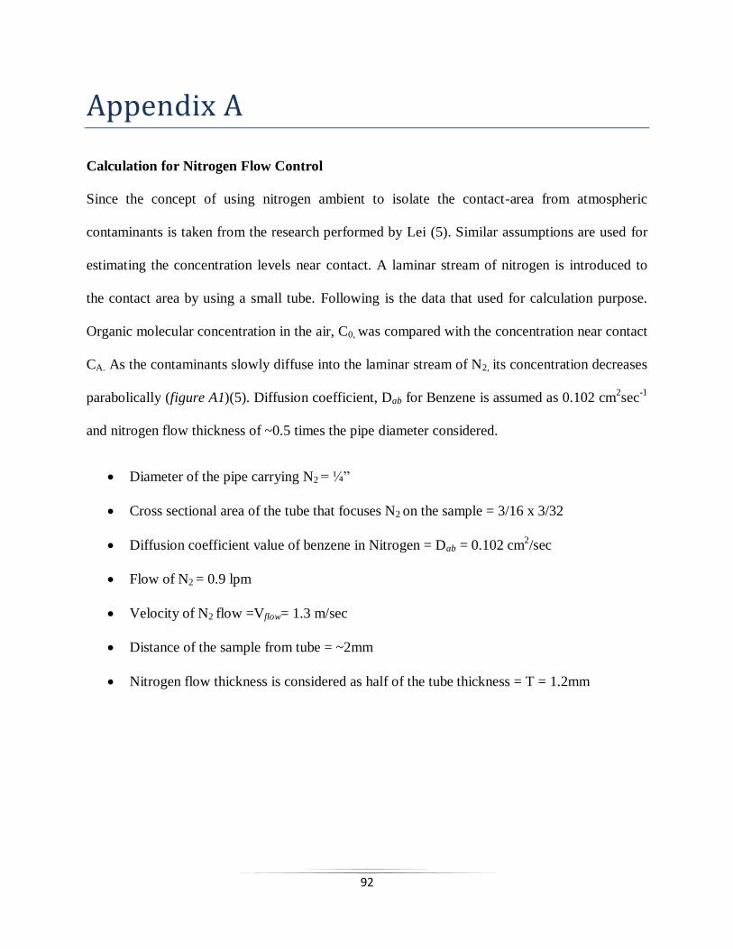
92
Appendix A
Calculation for Nitrogen Flow Control
Since the concept of using nitrogen ambient to isolate the contact-area from atmospheric
contaminants is taken from the research performed by Lei (5). Similar assumptions are used for
estimating the concentration levels near contact. A laminar stream of nitrogen is introduced to
the contact area by using a small tube. Following is the data that used for calculation purpose.
Organic molecular concentration in the air, C0, was compared with the concentration near contact
CA. As the contaminants slowly diffuse into the laminar stream of N2, its concentration decreases
parabolically (figure A1)(5). Diffusion coefficient, Dab for Benzene is assumed as 0.102 cm2sec
-1
and nitrogen flow thickness of ~0.5 times the pipe diameter considered.
Diameter of the pipe carrying N2 = ¼”
Cross sectional area of the tube that focuses N2 on the sample = 3/16 x 3/32
Diffusion coefficient value of benzene in Nitrogen = Dab = 0.102 cm2/sec
Flow of N2 = 0.9 lpm
Velocity of N2 flow =Vflow= 1.3 m/sec
Distance of the sample from tube = ~2mm
Nitrogen flow thickness is considered as half of the tube thickness = T = 1.2mm

93
= erfc
Based on the above calculations, the concentration level of organic contaminants was ten orders
of magnitude lower than that in air. It is important to note that the samples remain on the
corresponding holders at the angle of 120 to the flow. They are always switching while
conducting the tests which can make the laminar flow unsteady. Hence, the calculations given
above only give some estimation of the efficiency of N2 flow. For the simplicity in calculation
for determining the turbulent flow regime, Reynold’s number (Re) is assumed to be 580 for
steady jet flow (42). Pipe radius assumed to be equal to 2 mm and kinematic viscosity for
nitrogen can be taken as 1.52 *10-5
m2/s (43). Q can be calculated from Re as,
Q =
where Q is the flow rate, L is the characteristic length of pipe i.e. pipe diameter, v is
kinematic viscosity of nitrogen and A is cross sectional area of pipe. Based on this calculation
the limiting flow can be estimated as 1.62 lpm before it gets converted into turbulent regime.
Figure A1 Concentration Profile

94
Appendix B
Calculations for Designing Roughing Hose Diameter
The specified chamber-pressure for turning on the plasma-generator for Ar is 1 to 4 torr and the
flow of the gas required is 1 to 4slpm. Since the system is used for different gasses with Ar
continuously flowing through the plasma-generator, for the design purpose, it is assumed that the
chamber will be maintained at 2 torr with the total flow of the gas equal to 3slpm. The working
as is considered as air.
i.e. Q = 3 slpm = 0.05 lps
Assuming viscous flow,
Conductance, C for the hose is given as (35),
Cair,200
C =135.
L.s
-1
For our system, length of the pipe =120 inch
P’ =
Where P1 = Pressure maintained inside the chamber = 2 torr
P2 = Pressure downstream = 100mtorr (assumption)
Hence, P’ = 1.05 torr
Cair,200
C = 135.
------------------------------------------------------------------------------- (1)

95
The resistance offered by the length pipe is defined by (36),
R =
=
R = 38 torr.s/l ---------------------------------------------------------------------------------------- (2)
Cair,200
C =
Comparing equations (1) and (2)
d = 0.4 inch
However, the smallest inner diameter of the commercially available roughing hose was 0.74”
with the outer diameter of 0.75”.
So, before installing the pipe with these dimensions, it is necessary to do a check for chocking.
Chocking pressure P*= 2.3.
P*= 2.3.
≈ 42 mtorr
Since P* is still lesser that 100mtorr (assumed pressure downstream), chocking will not occur.
Now, let’s check the type of flow that would occur in the system.
Knudsen number is given as
Kn =
l’ = mean free path of the gas

96
d = pipe diameter
Kn =
Where lp
’ = variation of l’ with respect to pressure expressed in cm.mbar
For airat T=293 K, lp’ = 6.5*10
-3 cm-mbar
Hence,
Kn= 1.3*10-3
< 0.01
So, the flow comes under viscous continuum.
Calculation for Reynold’s number to determine if the flow is turbulent or laminar.
Re =
Re =
Re = 1158.35 < 2300
Thus, the flow is laminar.

97
Appendix C
Vacuum Chamber
Figure C1 represents the schematic drawing of the chamber that is used to generate plasma. It is provided
with 2 KF16 Fittings for inserting electrical feed-throughs, for doing four wire resistance measurements.
UV lamp can be directly fit from the front of the chamber by making the use of 15mm compression
fitting. KF 25 port is provided for attaching a pressure gauge while KF40 flange helps in attaching the
plasma source generator to the chamber.
Figure C1: - Plasma Chamber
KF 16 Fitting for Electrical
Feedthroughs
UV Lamp (Hamamatsu L2D27292)

98
Appendix D
Lifting Structure
Figure D1 shows the drawing of the lifting structure that is connected at the back of JEOL SPM.
Three horizontal bars provided on the structure support pulleys that guide a metallic rope from
winch to the plasma source generator.
Figure D1 Lifting Structure

99
Appendix E
Figure E1: - Drawing of the Clamp Fixed Inside AFM for Holding N2 Tube Near Contact
Figure E2: - Drawing of Tube Carrying N2 Near Contact

100
Bibliography
1. Rebeiz, Gabriel , "RF MEMS THEORY, DESIGN, AND TECHNOLOGY ".
2. Milosavljevic, Zlatoljub D. , "RF MEMS Switches : Microwave Review" , June 2004.
3. Elliott R. Brown, "RF-MEMS Switches for Reconfigurable Integrated Circuits". IEEE
TRANSACTIONS ON MICROWAVE THEORY AND TECHNIQUES, Novenmber 1998, Vol.
46.
4. Varadan, Vijay K.j. Vinoy K. A. Jose, "RF MEMS AND THEIR APPLICATIONS"
5. Chen, Dr. Lei, "Contact Evolution in Micromechanical Switches: an experimental
investigation using a contact test station", Northesirtheastern University,PhD thesis ,Aug 2007.
6. Sumit Majumder, N.E. McGruer, Geroge G Adams, P.M. Zavrasky, Richard Morrison,
Jacqueline Krim, "Study of contact in an electrostatically actuated microswitch" A 93 (19-26),
s.l. : ELSEVIER, 2001, Vol. Sensors and Actuators .
7. Chow, Linda L. W., "Lifetime Extension of RF MEMS Direct Contact Switches in Hot
Switching Operations by Ball Grid Array Dimple Design" s.l. : IEEE ELECTRON DEVICE
LETTERS, June 2007, Vol. 28.
8. Qing Ma, Quan Tran, Tsung-Kuan A. Chou, John Heck, Hanan Bar, Rishi Kant and Valluri
Rao, "Metal contact reliability of RF MEMS Switches" s.l. Intel Corporation, Santa Clara, CA
95054.
101
9. Feixiang Ke, Jianmin Miao, and Joachim Oberhammer, "A Ruthenium-Based Multimetal-
Contact RF MEMS Switch With a Corrugated Diaphragm" s.l. : JOURNAL OF
MICROELECTROMECHANICAL SYSTEMS,, Dec 2008, Vol. 17.
10. Kim, Yong Shi and Sang-Gook, "A Lateral, Self-cleaning, Direct Contact MEMS Switch"
s.l. : IEEE MEMS, 2005.
11. Hyouk KWON, Jae-Hyoung PARK3, Hee-Chul LEE4, Dong-Jun CHOI, "Investigation of
Similar and Dissimilar Metal Contacts for Reliable Radio Frequency Micorelectromechanical
Switches" 2008, s.l. : Japanese Journal of Applied Physics, 2008, Vols. 47, No. 8, pp. 6558–
6562.
12. T. Umemoto, T. Takeuchi, and R. Tanaka, "The behavior of surface oxide film on ruthenium
and rhodium plated contacts" s.l. : IEEE Trans.Compon., Hybrids, Manuf. Technol, Mar. 1978.,
Vols. vol. CHMT-1, no. 1,pp. 103–107,.
13. S. Umemura, K. Yasuda, and T. Aoki, “Contact resistance characteristics of noble metal
alloys for connector contacts" , s.l. : IEEE Trans.Compon., Hybrids, Manuf. Technol, March
1992, Vol. vol. 14 pp. 181–186.
14. Z Yang, D Lichtenwalner, A Morris, S Menzel, "A new test facility for efficient evaluation".,
s.l. : JOURNAL OF MICROMECHANICS AND MICROENGINEERING 2007, Vols. 17
(1788–1795).
15. Kevin W. Gilbert1, Shankar Mall1, Kevin D. Leedy2, Bryan Crawford, "A Nanoindenter
Based Method for Studying MEMS Contact Switch Microcontacts" s.l. : Holms Conference,
2008.

102
16. . Esa M. Yunus, John W. McBride, and Simon M. Spearing, "The Relationship Between
Contact Resistance and Contact Force on Au-Coated Carbon Nanotube Surfaces Under Low
Force Condition", No.3 s.l. : IEEE TRANSACTIONS ON COMPONENTS AND PACKAGING
TECHNOLOGIES, SEPTEMBER 2009, VOL. 32.
17. Daniel J. Dickrell, III and Michael T. Dugger, "Electrical Contact Resistance Degradation of
a Hot-Switched Simulated Metal MEMS Contact", NO. 1, s.l. : IEEE TRANSACTIONS ON
COMPONENTS AND PACKAGING TECHNOLOGIES,, MARCH 2007, Vol. VOL. 30.
18. A. Belkind, S. Gershman, "Plasma Cleaning of Surfaces. s.l. : Vacuum technology and
coating", 2008.
19. T. García, E. Nascimento, E. Bittencourt, "Plasma Processes as a CleanerAlternative for
Cleaning, Corrosion Resistance, and Functionalization of Metallic Surfaces", s.l. : International
Workshop in Cleaner Production, Vol. 2.
20. Remote RF Oxygen Plasma Cleaning of the Photoresist Residue and RIE-Related
Fluorocarbon Films. 2, s.l. : Journal of the Korean Physical Society,, Aug 2002, Vol. 11.
21. Manual Plasma Cleaning of electronic materials. s.l. : AST Products Inc.
22. VIG, JOHN R., "UV/ Ozone Cleaning of Surfaces", s.l. : IEEE TRANSACTIONS ON
PARTS, HYBRIDS, AND PACKAGING, VOL, DECEMBER 1976, Vols. VOL. PHP-12, NO.
4.
23. Suzanne Conroy, Ron Nickerson, Min-Shyan Sheu, "Plasma Cleaning of Medical Devices",
June 2000.
103
24. Soo Young Kim, 1 Kihyon Hong,1 Kisoo Kim,1 Hak Ki Yu,1 Woong-Kwon Kim,1 and
Jong-Lam Lee1, "Effect of N2, Ar, and O2 plasma treatments on surface properties of metals"
s.l. : JOURNAL OF APPLIED PHYSICS, 2008, Vols. 103, 076101.
25. www.allaboutcircuits.com. [Online] http://www.allaboutcircuits.com/vol_1/chpt_8/9.html.
26. Slade, Paul G. "Electrical Contacts Principles and Applications", s.l. : Marcel Dekker, Inc.
27. H. Eid, L. Chen, N. Joshi, N. E. McGruer, G. G. Adams, "Contact And Adhesion of Elastic-
plastc Layered Microsphere", San Francisco, California, USA : Proceedings of the STLE/ASME
2010 International Joint Tribology Conference, October 17-20, 2010,.
28. Lloyd, David H. hypertextbook.com. [Online]
http://hypertextbook.com/facts/2004/JennelleBaptiste.shtml.
29. Manual, Ansys 11.0 Reference.
30. The interrelation between adhesion, contact creep, and roughness on the life of gold contacts
in radio-frequency microswitches. s.l. : JOURNAL OF APPLIED PHYSICS, 2006.
31. Kevin W. Gilbert1, Shankar Mall1, Kevin D. Leedy2, Bryan Crawford, "A Nanoindenter
Based Method for Studying MEMS Contact Switch Microcontact", s.l. : Holms Conference,
2008.
32. Tomomi Sakata, Yuichi Okabe, Kei Kuwabara, Norio Sato, Kazuyoshi Ono,"Surface
Cleaning of Gold Structure by Annealing during Fabrication of Microelectromechanical System
Devices", s.l. : Japanese Journal of Applied Physics, 2009, Vol. 48 (2009) 026501.
33.www-bsac.EECS.Berkeley.EDU.

104
http://www-bsac.EECS.Berkeley.EDU/~pister/245/.
34. Ming-Tzer Lin a, Richard R. Chromik b, Nicholas Barbosa III b, Paul El-Deiry b, Seungmin
Hyun b, "The influence of vanadium alloying on the elevated-temperature mechanical properties
of thin gold film", 515 (2007) 7919–7925, s.l. : Science Direct, 2007.
35. Morris, D. J. Hucknall A. "Vaccum Technology calculations in chemistry". s.l. : RS.C.
36. Riviere, A. H. Rurnbull R. S. Barton J.C. "AN INTRODUCTION TO VACUUM
TECHNIQUE". s.l. : Wiley.
37. Manual, DI SPM. s.l. : Veeco Metrology group.
38. www.astricon.net. [Online] http://www.astricon.net/topics/broadband-mobile/articles/12581-
rf-mems-switches-deliver-early-promise.htm.
39. Mr. Vince Sieracki- Naval Air Systems, "Advances in MEMs for RF Technology", s.l. : 2000
AOC Radar and EW Conference Session 2:Technology Developments & Impact on Radar/ESM,
Oct 2000.
40. L. Chen, Z.J. Guo, N. Joshi, H. Eid, G.G. Adams and N.E. McGruer, "An SPM-Based
Contact Tester For Study Of Microcontacts", South Carolina USA : Hilton Head, June 2010.
41. L. Chen, H. Lee, Z. Guo, N.E.McGruer, K.W. Gilbert, S. Mall, L.D. Leedy, G.G. Adams, "
“Contact Resistance Study of Noble Metals and Alloy Films Using a Scanning Probe Microscope
Test Station,” Journal of Applied Physics, Vol. 102, 2007 074910, pp. 1-7.
42. Nawaf H. Saed, "Effect of Oscillating Jet Velocity on the Jet Impingement Cooling of an
isothermal surface" Scientific Research, Engineering, Nov 2009, 1, 133-139

105
43. http://www.lmnoeng.com/fluids.htm
44. http://www.i-micronews.com/interview.asp?id=25