an introduction to dram - catalogimages.wiley.com · 1-kilobit (kb) generation to the recent...
TRANSCRIPT

Chapter
1
An Introduction to DRAMDynamic random access memory (DRAM) integrated circuits (ICs) haveexisted for more than twenty-five years. DRAMs evolved from the earliest1-kilobit (Kb) generation to the recent 1-gigabit (Gb) generation throughadvances in both semiconductor process and circuit design technology. Tre-mendous advances in process technology have dramatically reduced featuresize, permitting ever higher levels of integration. These increases in integra-tion have been accompanied by major improvements in component yield toensure that overall process solutions remain cost-effective and competitive.Technology improvements, however, are not limited to semiconductor pro-cessing. Many of the advances in process technology have been accompa-nied or enabled by advances in circuit design technology. In most cases,advances in one have enabled advances in the other. In this chapter, weintroduce some fundamentals of the DRAM IC, assuming that the readerhas a basic background in complementary metal-oxide semiconductor(CMOS) circuit design, layout, and simulation [1].
1.1 DRAM TYPES AND OPERATION
To gain insight into how modern DRAM chips are designed, it is useful tolook into the evolution of DRAM. In this section, we offer an overview ofDRAM types and modes of operation.
1.1.1 The 1k DRAM (First Generation)
We begin our discussion by looking at the 1,024-bit DRAM (1,024 x1 bit). Functional diagrams and pin connections appear in Figure 1.1 andFigure 1.2, respectively. Note that there are 10 address inputs with pinlabels R\~Rs and C\-C5. Each address input is connected to an on-chipaddress input buffer. The input buffers that drive the row (R) and column

2 Chap. 1 An Introduction to DRAM
(C) decoders in the block diagram have two purposes: to provide a knowninput capacitance (CM) on the address input pins and to detect the inputaddress signal at a known level so as to reduce timing errors. The levelVTRIP> an idealized trip point around which the input buffers slice the inputsignals, is important due to the finite transition times on the chip inputs(Figure 1.3). Ideally, to avoid distorting the duration of the logic zeros andones, VTRIP should be positioned at a known level relative to the maximumand minimum input signal amplitudes. In other words, the reference levelshould change with changes in temperature, process conditions, input maxi-mum amplitude (Vm), and input minimum amplitude (VIL). Having saidthis, we note that the input buffers used in first-generation DRAMs weresimply inverters.
Continuing our discussion of the block diagram shown in Figure 1.1,we see that five address inputs are connected through a decoder to the1,024-bit memory array in both the row and column directions. The totalnumber of addresses in each direction, resulting from decoding the 5-bitword, is 32. The single memory array is made up of 1,024 memory elementslaid out in a square of 32 rows and 32 columns. Figure 1.4 illustrates theconceptual layout of this memory array. A memory element is located at theintersection of a row and a column.
Vss VDD °I C 2 C3 CA Cs
? _ _ i — ? ? ? ? ? , 1Address inputbuffers
UCE O - ^ j C-decoder |
U QD W O • Buffer —^ SSpKre^ 1 1 * Buffer - ^ - - O O o a r
f W O *- Buffer *
R, O - * - I
Figure 1.1 1,024-bit DRAM functional diagram.

Figure 1.3 Ideal address input buffer.
By applying an address of all zeros to the 10 address input pins, thememory data located at the intersection of rowO, RAO, and column 0, CAO, isaccessed. (It is either written to or read out, depending on the state of the R/Winput and assuming that the CE pin is LOW so that the chip is enabled.)
It is important to realize that a single bit of memory is accessed by usingboth a row and a column address. Modern DRAM chips reduce the numberof external pins required for the memory address by using the same pins for
Sec. 1.1 DRAM Types and Operation 3
c2 1 Q • ]]i6 c3
Ci 2 [ ^15 C4
BW3([ [ ] ]14 C5
R2 4 C ]13 CE
fls 5 [ ]]12 DQUT
«4 6[ [ j ]11 D//v
fls 7 [ ]1O \/ss
«i 8 [ ] 9 VDD
Figure 1.2 1,024-bit DRAM pin connections.
Input signal +ss^ Input bufferPad ^ s ^ ^Output to
I I Vmp - / •decoders
Inputsignal VfH
/; ;* Vk
1 I Output signali i
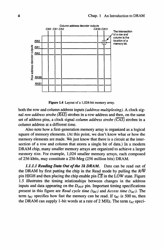
Figure 1.4 Layout of a 1,024-bit memory array.
both the row and column address inputs (address multiplexing). A clock sig-nal row address strobe (RAS) strobes in a row address and then, on the sameset of address pins, a clock signal column address strobe (CAS) strobes in acolumn address at a different time.
Also note how a first-generation memory array is organized as a logicalsquare of memory elements. (At this point, we don't know what or how thememory elements are made. We just know that there is a circuit at the inter-section of a row and column that stores a single bit of data.) In a modernDRAM chip, many smaller memory arrays are organized to achieve a largermemory size. For example, 1,024 smaller memory arrays, each composedof 256 kbits, may constitute a 256-Meg (256 million bits) DRAM.
1.1.1.1 Reading Data Out of the Ik DRAM. Data can be read out ofthe DRAM by first putting the chip in the Read mode by pulling the R/Wpin HIGH and then placing the chip enable pin "CE in the LOW state. Figure1.5 illustrates the timing relationships between changes in the addressinputs and data appearing on the DQUT pin. Important timing specificationspresent in this figure are Read cycle time (tRC) and Access time (tAC)- Theterm tRC specifies how fast the memory can be read. If tRC is 500 ns, thenthe DRAM can supply 1-bit words at a rate of 2 MHz. The term tAC speci-
4 Chap. 1 An Introduction to DRAM
Column address decoder outputsCAO CA\ CA2 CA30 CAM
The intersectionI I I I I /o\ a row and
/column is thelocation of a
v *? memory bit.f R41
2 5d2CD
0)
i(0
| ft/130
fty431
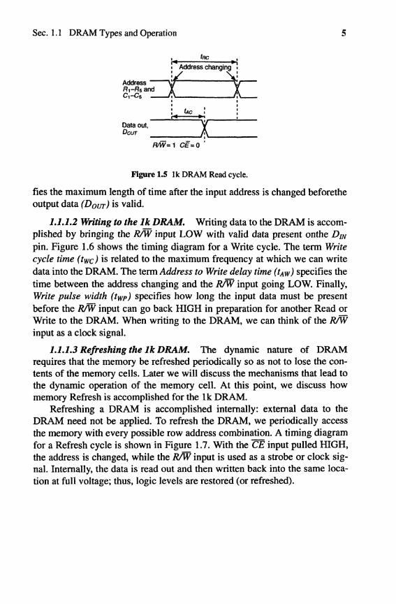
Figure 1.5 Ik DRAM Read cycle.
fies the maximum length of time after the input address is changed beforetheoutput data (Dour) is valid.
1.1.1.2 Writing to the ikJDRAM. Writing data to the DRAM is accom-plished by bringing the R/W input LOW with valid data present onthe DiN
pin. Figure 1.6 shows the timing diagram for a Write cycle. The term Writecycle time (twc) is related to the maximum frequency at which we can writedata into the DRAM. The term Address to Write delay time (tAW) specifies thetime between the address changing and the R/W input going LOW. Finally,Write pulse width (tWP) specifies how long the input data must be presentbefore the R/W input can go back HIGH in preparation for another Read orWrite to the DRAM. When writing to the DRAM, we can think of the R/Winput as a clock signal.
1.1.1.3 Refreshing the Ik DRAM. The dynamic nature of DRAMrequires that the memory be refreshed periodically so as not to lose the con-tents of the memory cells. Later we will discuss the mechanisms that lead tothe dynamic operation of the memory cell. At this point, we discuss howmemory Refresh is accomplished for the Ik DRAM.
Refreshing a DRAM is accomplished internally: external data to theDRAM need not be applied. To refresh the DRAM, we periodically accessthe memory with every possible row address combination. A timing diagramfor a Refresh cycle is shown in Figure 1.7. With the CE input pulled HIGH,the address is changed, while the R/W input is used as a strobe or clock sig-nal. Internally, the data is read out and then written back into the same loca-tion at full voltage; thus, logic levels are restored (or refreshed).
Sec. 1.1 DRAM Types and Operation 5
H 5S *• Address changing •
\s vAddress ~~~^T T/
%% al_I L• i
S, to .; iData out, VDour A
fW=1 C£=0 '

Figure 1.7 Ik DRAM Refresh cycle.
1 J.I.4 A Note on the Power Supplies, The voltage levels used in theIk DRAM are unusual by modern-day standards. In reviewing Figure 1.2,we see that the Ik DRAM chip uses two power supplies: VDD and Vss. Tobegin, V ^ is a greater voltage than VDD: VSs is nominally 5 V, while VDD is-12 V. The value of VSs was set by the need to interface to logic circuits thatwere implemented using transistor-transistor logic (TTL) logic. The 17-Vdifference between VDD and VSs was necessary to maintain a large signal-to-noise ratio in the DRAM array. We discuss these topics in greater detail laterin the book. The VSs power supply used in modern DRAM designs, at thetime of this writing, is generally zero; the VDD is in the neighborhood of2.5 V.
6 Chap. 1 An Introduction to DRAM
j^^j y+— < 50 ns
« I \»« wc » j ; ^ ^ o n s
Address X I Xj « ^ » i < twp w\
R/W / ! \ /
Data V VinP"t A A
Figure 1.6 Ik DRAM Write cycle.
i* ** >iRow v/ vyaddress V Yi nPu t s A A
i i
«w / i\ x{CE=1 J :

Sec. 1.1 DRAM Types and Operation 7
Ll.1.5 The 3-Transistor DRAM Cell One of the interesting circuitsused in the Ik DRAM (and a few of the 4k and 16k DRAMs) is the 3-transis-tor DRAM memory cell shown in Figure 1.8. The column- and rowlinesshown in the block diagram of Figure 1.1 are split into Write and Read linepairs. When the Write rowline is HIGH, Ml turns ON. At this point, the datapresent on the Write columnline is passed to the gate of M2, and the informa-tion voltage charges or discharges the input capacitance of M2. The next, andfinal, step in writing to the mbit cell is to turn OFF the Write rowline by driv-ing it LOW. At this point, we should be able to see why the memory is calleddynamic. The charge stored on the input capacitance of M2 will leak off overtime.
Figure 1.8 3-transistor DRAM cell.
If we want to read out the contents of the cell, we begin by first precharg-ing the Read columnline to a known voltage and then driving the Read row-line HIGH. Driving the Read rowline HIGH turns M3 ON and allows M2either to pull the Read columnline LOW or to not change the prechargedvoltage of the Read columnline. (If M2's gate is a logic LOW, then M2 willbe OFF, having no effect on the state of the Read columnline.) The maindrawback of using the 3-transistor DRAM cell, and the reason it is no longerused, is that it requires two pairs of column and rowlines and a large layoutarea. Modern 1-transistor, 1-capacitor DRAM cells use a single rowline, asingle columnline, and considerably less area.
1.1.2 The 4k-64 Meg DRAM (Second Generation)
We distinguish second-generation DRAMs from first-generationDRAMs by the introduction of multiplexed address inputs, multiple memory
Write columnline Read columnline
Read rowline • —
Write rowline # - 4 -
< J J MCM 2
Input / I. Vcapacitance V Storage node0fM2
8 Chap. 1 An Introduction to DRAM
arrays, and the 1-transistor/1-capacitor memory cell. Furthermore, second-generation DRAMs offer more modes of operation for greater flexibility orhigher speed operation. Examples are page mode, nibble mode, static col-umn mode, fast page mode (FPM), and extended data out (EDO). Second-generation DRAMs range in size from 4k (4,096 x 1 bit, i.e., 4,096 addresslocations with 1-bit input/output word size) up to 64 Meg (67,108,864 bits)in memory sizes of 16 Meg x 4 organized as 16,777,216 address locationswith 4-bit input/output word size, 8 Meg x 8, or 4 Meg x 16.
Two other major changes occurred in second-generation DRAMs:(1) the power supply transitioned to a single 5 V and (2) the technologyadvanced from NMOS to CMOS. The change to a single 5 V supplyoccurred at the 64kbit density. It simplified system design to a single powersupply for the memory, processor, and any TTL logic used in the system. Asa result, rowlines had to be driven to a voltage greater than 5 V to turn theNMOS access devices fully ON (more on this later), and the substrate heldat a potential less than zero. For voltages outside the supply range, chargepumps are used (see Chapter 6). The move from NMOS to CMOS, at the1Mb density level, occurred because of concerns over speed, power, andlayout size. At the cost of process complexity, complementary devicesimproved the design.
1.1.2.1 Multiplexed Addressing. Figure 1.9 shows a 4k DRAM blockdiagram, while Figure 1.10 shows the pin connections for a 4k chip. Notethat compared to the block diagram of the Ik DRAM shown in Figure 1.1,the number of address input pins has decreased from 10 to 6, even thoughthe memory size has quadrupled. This is the result of using multiplexedaddressing in which the same address input pins are used for both the rowand column addresses. The row address strobe (RAS) input clocks theaddress present on the DRAM address pins Ao to A5 into the row addresslatches on the falling edge. The column address strobe (CAS) input clocksthe input address into the column address latches on its falling edge.
Figure 1.11 shows the timing relationships between RAS9 CAS, and theaddress inputs. Note that tRC is still (as indicated in the last section) the ran-dom cycle time for the DRAM, indicating the maximum rate we can writeto or read from a DRAM. Note too how the row (or column) address mustbe present on the address inputs when RAS (or CAS) goes LOW. The param-eters tMs and tCAs indicate how long RAS or CAS must remain LOW afterclocking in a column or row address. The parameters tASR9 r^//, tASCy andtcAH indicate the setup and hold times for the row and column addresses,respectively.

Sec. 1.1 DRAM Types and Operation 9
tColumn address latches
CAS • ! _"
Column decoder
1/ 32/^"g . Q ,
Ao~~ % I ArrayO(2k) J^ t a ^^
^3— •- -o ^ 1 X 1
>\s— S ff Array1(2k)
Figure 1.9 Block diagram of a 4k DRAM.
VBB 1 [ • D^6 vss
D,N 2 ^ ] 75 CAS
FUW 3 Q ] ) 4 Dour
RAS 4 C ]73 CS
1 6C [ ] D " 4A2 7 £ DtO >A5
VDD 8 ([ 3 9 vcc
Figure 1.10 4,096-bit DRAM pin connections.

10 Chap. 1 An Introduction to DRAM
Figure 1.11 Address timing.
1.1.2.2 Multiple Memory Arrays. As mentioned earlier, second-gen-eration DRAMs began to use multiple or segmented memory arrays. Themain reason for splitting up the memory into more than one array at the costof a larger layout area can be understood by considering the parasiticspresent in the dynamic memory circuit element. To understand the originsof these parasitics, consider the modern DRAM memory cell comprisingone MOSFET and one capacitor, as shown in Figure 1.12.
In the next section, we cover the operation of this cell in detail. Here weintroduce the operation of the cell. Data is written to the cell by driving therowline (a.k.a., wordline) HIGH, turning ON the MOSFET, and allowingthe columnline (a.k.a., digitline or bitline) to charge or discharge the storagecapacitor. After looking at this circuit for a moment, we can make the fol-lowing observations:
1. The wordline (rowline) may be fabricated using polysilicon (poly).This allows the MOSFET to be formed by crossing the poly wordlineover an n+ active area.
2. To write a full VCc logic voltage (where VCc is the maximum positivepower supply voltage) to the storage capacitor, the rowline must bedriven to a voltage greater than Vcc + the n-channel MOSFETthreshold voltage (with body effect). This voltage, > Vcc + VTH, isoften labeled VCc pumped (VCCp).
3. The bitline (columnline) may be made using metal or polysilicon.The main concern, as we'll show in a moment, is to reduce the para-sitic capacitance associated with the bitline.
S- — * Hi IRAS I i
~—y 'r-iCAS ; 0- . ^ * y
I I t *
U« »^4 ^J ^SC tCAH •
77" W Row V ; Column j VAddresses ^ address y\ i address ; J\
• i t •• i t ii i i i

Sec. 1.1 DRAM Types and Operation 11
Figure 1.12 1-transistor, 1-capacitor (1T1C) memory cell.
Consider the row of N dynamic memory elements shown in Figure 1.13.Typically, in a modern DRAM, N is 512, which is also the number of bitlines.When a row address is strobed into the DRAM, via the address input pinsusing the falling edge of RAS, the address is decoded to drive a wordline(rowline) to VQCP- This turns ON an entire row in a DRAM memory array.Turning ON an entire row in a DRAM memory array allows the informationstored on the capacitors to be sensed (for a Read) via the bitlines or allowsthe charging or discharging, via the bitlines, of the storage capacitors (for aWrite). Opening a row of data by driving a wordline HIGH is a very impor-tant concept for understanding the modes of DRAM operation. For Refresh,we only need to supply row addresses during a Refresh operation. For pageReads—when a row is open—a large amount of data, which is set by thenumber of columns in the DRAM array, can be accessed by simply changingthe column address.
We're now in a position to answer the question: "Why are we limited toincreasing the number of columnlines (or bitlines) used in a memory array?"or "Why do we need to break up the memory into smaller memory arrays?"The answer to these questions comes from the realization that the more bit-lines we use in an array, the longer the delay through the wordline (see Figure1.13).
If we drive the wordline on the left side of Figure 1.13 HIGH, the signalwill take a finite time to reach the end of the wordline (the wordline on theright side of Figure 1.13). This is due to the distributed resistance/capaci-tance structure formed by the resistance of the polysilicon wordline and thecapacitance of the MOSFET gates. The delay limits the speed of DRAMoperation. To be precise, it limits how quickly a row can be opened andclosed. To reduce this RC time, a polycide wordline is formed by adding asilicide, for example, a mixture of a refractory metal such as tungsten with
Digitline orcolumnline oroffline
_ .for rowline »L— „
Is
Storage capaci tor^ J»

Figure 1.13 Row of N dynamic memory elements.
polysilicon, on top of polysilicon. Using a polycide wordline will have theeffect of reducing the wordline resistance. Also, additional drivers can beplaced at different locations along the wordline, or the wordline can bestitched at various locations with metal.
The limitations on the additional number of wordlines can be under-stood by realizing that by adding more wordlines to the array, more parasiticcapacitance is added to the bitlines. This parasitic capacitance becomesimportant when sensing the value of data charge stored in the memory ele-ment. We'll discuss this in more detail in the next section.
1.1.2.3 Memory Array Size. A comment is in order about memoryarray size and how addressing can be used for setting word and page size.(We'll explain what this means in a moment.) If we review the block dia-gram of the 4k DRAM shown in Figure 1.9, we see that two 2k-DRAMmemory arrays are used. Each 2k memory is composed of 64 wordlines and32 bitlines for 2,048 memory elements/address locations per array. In theblock diagram, notice that a single bit, coming from the column decoder,can be used to select data, via the bitlines, from ArrayO or Array 1.
From our discussion earlier, we can open a row in ArrayO while at thesame time opening a row in Array 1 by simply applying a row address to theinput address pins and driving RAS LOW. Once the rows are open, it is asimple matter of changing the column address to select different data asso-ciated with the same open row from either array. If our word size is 1 bit, wecould define a page as being 64 bits in length (32 bits from each array). Wecould also define our page size as 32 bits with a 2-bit word for input/output.We would then say that the DRAM is a 4k DRAM organized as 2k x 2. Ofcourse, in the 4k DRAM, in which the number of bits is small, the conceptsof page reads or size aren't too useful. We present them here simply to illus-trate the concepts. Let's consider a more practical and modern configura-tion.
12 Chap. 1 An Introduction to DRAM
BitiineO Bitlinei BitlineN-2 BitlineN-1
Wordline I ° F^' [""" I n
From driver is. I I I I
EH>^—T^A—T~I J J J

Sec. 1.1 DRAM Types and Operation 13
Suppose we have a 64-Meg DRAM organized as 16 Meg x4 (4 bitsinput/output) using 4k row address locations and 4k column address loca-tions (12 bits or pins are needed for each 4k of addressing). If our (sub)memory array size is 256kbits, then we have a total of 256 memory arrays onour DRAM chip. We'll assume that there are 512 wordlines and 512 bitlines(digitlines), so that the memory array is logically square. (However, physi-cally, as we shall see, the array is not square.) Internal to the chip, in theaddress decoders, we can divide the row and column addresses into twoparts: the lower 9 bits for addressing the wordlines/bitlines in a 256k mem-ory array and the upper 3 bits for addressing one of the 64 "group-of-four"memory arrays (6 bits total coming from the upper 3 bits of the row and col-umn addresses).
Our 4-bit word comes from the group-of-four memory arrays (one bitfrom each memory array). We can define a page of data in the DRAM byrealizing that when we open a row in each of the four memory arrays, we areaccessing 2k of data (512 bits/array x 4 arrays). By simply changing the col-umn address without changing the row address and thus opening anothergroup-of-four wordlines, we can access the 2k "page" of data. With a littleimagination, we can see different possibilities for the addressing. For exam-ple, we could open 8 group-of-four memory arrays with a row address andthus increase the page size to 16k, or we could use more than one bit at atime from an array to increase word size.
1.1.2.4 Refreshing the DRAM. Refreshing the DRAM is accom-plished by sequentially opening each row in the DRAM. (We'll discuss howthe DRAM cell is refreshed in greater detail later in the book.) If we use the64-Meg example in the last section, we need to supply 4k row addresses tothe DRAM by changing the external address inputs from 000000000000 to111111111111 while clocking the addresses into the DRAM using the fallingedge of RAS. In some DRAMs, an internal row address counter is present tomake the DRAM easier to refresh. The general specification for 64-MegDRAM Refresh is that all rows must be refreshed at least every 64 ms,which is an average of 15.7 JJS per row. This means, that if the Read cycletime tRC is 100 ns (see Figure 1.11), it will take 4,096 • 100 ns or 410 ps torefresh a DRAM with 4k of row addresses. The percentage of time theDRAM is unavailable due to Refresh can be calculated as 410 JJS/64 ms or0.64% of the time. Note that the Refresh can be a burst, taking 410 JJS as justdescribed, or distributed, where a row is refreshed every 15.7 JJS.
1.1.2.5 Modes of Operation. From the last section, we know that wecan open a row in one or more DRAM arrays concurrently, allowing a page

14 Chap. 1 An Introduction to DRAM
of data to be written to or read from the DRAM. In this section, we look atthe different modes of operation possible for accessing this data via the col-umn address decoder. Our goal in this section is not to present all possiblemodes of DRAM operation but rather to discuss the modes that have beenused in second-generation DRAMs. These modes are page mode, nibblemode, static column mode, fast page mode, and extended data out.
Figure 1.14 shows the timing diagram for a page mode Read, Write, andRead-Modify-Write. We can understand this timing diagram by first notic-ing that when RAS goes LOW, we clock in a row address, decode the rowaddress, and then drive a wordline in one or more memory arrays to VCCP.The result is an open row(s) of data sitting on the digitlines (columnlines).Only one row can be opened in any single array at a time. Prior to openinga row, the bitlines are precharged to a known voltage. (Precharging to VCc/2is typically performed using internal circuitry.) Also notice at this time thatdata out, D0UT, is in a Hi-Z state; that is, the DRAM is not driving the busline connected to the DOUT pin.
The next significant timing event occurs when CAS goes LOW and thecolumn address is clocked into the DRAM (Figure 1.14). At this time, thecolumn address is decoded, and, assuming that the data from the open rowis sitting on the digitlines, it is steered using the column address decoder toDour- We may have an open row of 512 bits, but we are steering only onebit to DOUT- Notice that when CAS goes HIGH, D0UT goes back to the Hi-Zstate.
By strobing in another column address with the same open row, we canselect another bit of data (again via the column address decoder) to steer tothe Dour pin- In this case, however, we have changed the DRAM to theWrite mode (Figure 1.14). This allows us to write, with the same row openvia the DjN pin in Figure 1.10, to any column address on the open row.Later, second-generation DRAMs used the same pins for both data inputand output to reduce pin count These bidirectional pins are labeled DQ.
The final set of timing signals in Figure 1.14 (the right side) read dataout of the DRAM with R/W HIGH, change R/W to a LOW, and then write tothe same location. Again, when CAS goes HIGH, DOUT goes back to the Hi-Z state.
The remaining modes of operation are simple modifications of pagemode. As seen in Figure 1.15, FPM allows the column address to changewhile CAS is LOW. The speed of the DRAM improves by reducing thedelay between CAS going LOW and valid data present, or accessed, onDour OCAC)- EDO is simply an FPM DRAM that doesn't force D0UT to a Hi-Z state when CAS goes HIGH. The data out of the DRAM is thus available

Sec. 1.1 DRAM Types and Operation 15
for a longer period of time, allowing for faster operation. In general, openingthe row is the operation that takes the longest amount of time. Once a row isopen, the data sitting on the columnlines can be steered to DOVT at a fast rate.Interestingly, using column access modes has been the primary method ofboosting DRAM performance over the years.
The other popular modes of operation in second-generation DRAMswere the static column and nibble modes. Static column mode DRAMs usedflow-through latches in the column address path. When a column addresswas changed externally, with CAS LOW, the column address fed directly tothe column address decoder. (The address wasn't clocked on the falling edgeof CAS.) This increased the speed of the DRAM by preventing the outputsfrom going into the Hi-Z state with changes in the column address.
Figure 1.14 Page mode.
Nibble mode DRAMs used an internal presettable address counter sothat by strobing CAS, the column address would change internally. Figure1.16 illustrates the timing operation for a nibble mode DRAM. The first timeCAS transitions LOW (first being defined as the first transition after RASgoes LOW), the column address is loaded into the counter. If RAS is heldLOW and CAS is toggled, the internal address counter is incremented, andthe sequential data appears on the output of the DRAM. The term nibblemode comes from limiting the number of CAS cycles to four (a nibble).
!-« tRAS • !RAS"\ j /
1 i fcp i i tcp i
^TTl /Hi /Ht /ttAsc^ , \ : j «
5 ! ! ' ! ' * •I • J R A C - ^ — i I ; - * — • •
DouT ~ ( Valid ) — - \ 1 =t Valid )
^ 1 \; /—7 i V /—7
D/w yVai id^X )CvalicTy
|^ Read ^ j - * Write •j Read-Modify-Write ^

16 Chap. 1 An Introduction to DRAM
Figure 1.16 Nibble mode.
1.1.3 Synchronous DRAMs (Third Generation)
Synchronous DRAMs (SDRAMs) are made by adding a synchronousinterface between the basic core DRAM operation/circuitry of second-gen-eration DRAMs and the control coming from off-chip to make the DRAMoperation faster. All commands and operations to and from the DRAM areexecuted on the rising edge of a master or command clock signal that iscommon to all SDRAMs and labeled CLK. See Figure 1.17 for the pin con-nections of a 64Mb SDRAM with 16-bit input/output (I/O).
At the time of this writing, SDRAMs operate with a maximum CLK fre-quency in the range of 100-143 MHz. This means that if a 64Mb SDRAM
r* *RAS *-i
RAS y. ' •
i : : \josj I :
•I ' . » « i ' !
Dour ( Valid ) ( Valid ) (1^5"^ ( Valid )
FVW ////////
Figure 1.15 Fast page mode.
j-« tRAs • ;RAS V >
I I I I t I I I '1 • • i JNCP^ I i i
I -•!;-*-|ksc i ! !
I T>gy )£////////////////////////////////////////,< , i , i i i i
i I jgAC I i , • , i ,
Dour j (Valid) O^iidT) (Valid) (Valid)
Write'/////// X////,

Sec. 1.1 DRAM Types and Operation 17
Figure 1.17 Pin connections of a 64Mb SDRAM with 16-bit I/O.
is organized as a xl6 part (that is, the input/output word size is 16 bits), themaximum rate at which the words can be written to the part is 200-286MB/s.
Another variation of the SDRAM is the double-data-rate SDRAM (DDRSDRAM, or simply DDR DRAM). The DDR parts register commands andoperations on the rising edge of the clock signal while allowing data to betransferred on both the rising and falling edges. A differential input clocksignal is used in the DDR DRAM with the labeling of, not surprisingly, CLKand CLK. In addition, the DDR DRAM provides an output data strobe,labeled DQS, synchronized with the output data and the input CLK. DQS isused at the controller to strobe in data from a DRAM. The big benefit ofusing a DDR part is that the data transfer rate can be twice the clock fre-quency because data can be transferred on both the rising and falling edgesof CLK This means that when using a 133 MHz clock, the data written toand read from the DRAM can be transferred at 266M words/s. Using thenumbers from the previous paragraph, this means that a 64Mb DDR
VDD C E f 1 » ^ - ^ 54\D VSS
000 d 2 53 J3 D015VDDQ CE 3 52 X) VssQOQ1 CC 4 51 X) D O 1 4
OQ2 CC 5 50 I] OQ13^ssO [[ 6 49 X) OoODQ3 (X 7 48 X) 00120Q4 CC 8 47 X) M 1 1VDDO H 9 46 X) v$sQ005 CE 10 45 X) D O 1 0OQ6 CE 11 44 JJ °09VssQ CC 12 43 X) VDDQ007 CC 13 42 X) 008Voo CE 14 41 X ) VfesOQML CE 15 40 X3 WCWE CE 16 39 X) DQMHCAS CE 17 38 X ] C(JCRAS CE 18 37 X) C/CECS CC 19 36 X) WCBAQ CE 20 35 X) AnS/U CE 21 34 X3 A9
Ayo CE 22 33 D >»8Ao CC 23 32 XI A7
A\ CE 24 31 X ) >A6
A2 CC 25 30 X3 * 5A3 CC 26 29 XI A4
VDD CE\27 /^\ 28^D V s s

18 Chap. 1 An Introduction to DRAM
SDRAM with an input/output word size of 16 bits will transfer data to andfrom the memory controller at 400-572 MB/s.
Figure 1.18 shows the block diagram of a 64Mb SDRAM with 16-bitI/O. Note that although CLK is now used for transferring data, we still havethe second-generation control signals C5, WE, CAS, and RAS present on thepart. (CKE is a clock enable signal which, unless otherwise indicated, isassumed HIGH.) Let's discuss how these control signals are used in anSDRAM by recalling that in a second-generation DRAM, a Write was exe-cuted by first driving WE and VS LOW. Next a row was opened by applyinga row address to the part and then driving RAS LOW. (The row address islatched on the falling edge of RAS.) Finally, a column address was appliedand latched on the falling edge of CAS. A short time later, the data appliedto the part would be written to the accessed memory location.
For the SDRAM Write, we change the syntax of the descriptions ofwhat's happening in the part. However, the fundamental operation of theDRAM circuitry is the same as that of the second-generation DRAMs. Wecan list these syntax changes as follows:
1. The memory is segmented into banks. For the 64Mb memory of Fig-ure 1.17 and Figure 1.18, each bank has a size of 16Mbs (organizedas 4,096 row addresses [12 bits] x 256 column addresses [8 bits] x 16bits [16 DQ I/O pins]). As discussed earlier, this is nothing more thana simple logic design of the address decoder (although in most prac-tical situations, the banks are also laid out so that they are physicallyin the same area). The bank selected is determined by the addressesBAOandJSAl.
2. In second-generation DRAMs, we said, "We open a row," as dis-cussed earlier. In SDRAM, we now say, "We activate a row in abank." We do this by issuing an active command to the part. Issuingan active command is accomplished on the rising edge of CLK with arow/bank address applied to the part with VS and RAS LOW, whileCAS and WE are held HIGH.
3. In second-generation DRAMs, we said, "We write to a location givenby a column address," by driving CAS LOW with the column address

Sec. 1.1 DRAM Types and Operation 19
Figure 1.18 Block diagram of a 64Mb SDRAM with 16-bit I/O.
applied to the part and then applying data to the part. In an SDRAM,we write to the part by issuing the Write command to the part. Issuinga Write command is accomplished on the rising edge of CLK with acolumn/bank address applied to the part: CS, CAS, and WE are heldLOW, and RAS is held HIGH.
Table 1.1 shows the commands used in an SDRAM. In addition, thistable shows how inputs/outputs (DQs) can be masked using the DQ mask(DQM) inputs. This feature is useful when the DRAM is used in graphicsapplications.
ax-** ;
13 !||«- ^T" jj - 12 j 1 . E ~ K - i r1"?""^"""2-^ !
! 1 Mode register] ! [counter fr f i R o w . ^jtBankO fe BankO | i I O O M I
. I ^ ^ ^ 1 | L *duf ** " 5 g j ^ « S^V j i 2 2 j DOMH
| ^ ^ ' *y| decoder P \ 256x16) ,i • i • i J
i W, ' A l l I o^><- aM.r,nii,«, T 16 . „ _ !
BAO i ^ ' 2 , ^ | ' h-j^ #s VOgatingDQM ^ ^ ^ ^ " 16 ^ ^ ^ ( ^ ^ ^ ^
! tt " " • ' — " ^ ^ ^ ^ n ' j I re9istar ' !J ^ 256x16^*5 Column \ J! ? i I 1 n g l decoder j "
! ^ latch J

20 Chap. 1 An Introduction to DRAM
Table 1.1 SDRAM commands. (Notes: 1)
Name
Command inhibit(NOP)
No operation(NOP)
Active (selectbank andactivate row)
Read (selectbank and col-umn, and startRead burst)
Write (selectbank and col-umn, and startWrite burst)
Burst terminate
PRECHARGE(deactive row inbank or banks)
Auto-Refresh orSelf-Refresh(enter Self-Refresh mode)
Load mode regis-ter
WriteEnable/outputEnable
Write inhibit/out-put Hi-Z
CS
H
L
L
L
L
L
L
L
L
—
—
RAS
X
H
L
H
H
H
L
L
L
—
—
CAS
X
H
H
L
L
H
H
L
L
—
—
WE
X
H
H
H
L
L
L
H
L
—
—
DQM
X
X
X
L/H«
L/H8
X
X
X
X
L
H
ADDR
X
X
Bank/row
Bank/col
Bank/col
X
Code
X
Op-code
—
—
DQs
X
X
X
X
Valid
Active
X
X
X
Active
Hi-Z
Notes
—
—
3
4
4
—
5
6,7
2
8
8
Notes
1. CKE is HIGH for all commands shown except for Self-Refresh.2. AO-All define the op-code written to the mode register.3. AO-Al 1 provide row address, and BAO, BA\ determine which bank is made active.4. AQ-A9 (x4), A0-A8 (x8), or AO-Al (xl6) provide column address; A10 HIGH
enables the auto PRECHARGE feature (nonpersistent), while A10 LOW disables theauto PRECHARGE feature; BAO, BA\ determine which bank is being read from orwritten to.

Sec. 1.1 DRAM Types and Operation 21
5.A10 LOW: BAQ, BAl determine the bank being precharged. A\0 HIGH: all banks pre-charged and BAO, BA\ are "don't care."
6. This command is Auto-Refresh if CKE is HIGH and Self-Refresh if CKE is LOW.7. Internal Refresh counter controls row addressing; all inputs and I/Os are "don't care"
except for CKE.8. Activates or deactivates the DQs during Writes (zero-clock delay) and Reads (two-
clock delay).
SDRAMs often employ pipelining in the address and data paths toincrease operating speed. Pipelining is an effective tool in SDRAM designbecause it helps disconnect operating frequency and access latency. Withoutpipelining, a DRAM can only process one access instruction at a time.Essentially, the address is held valid internally until data is fetched from thearray and presented to the output buffers. This single instruction mode ofoperation ties operating frequency and access time (or latency) together.However, with pipelining, additional access instructions can be fed into theSDRAM before prior access instructions have completed, which permitsaccess instructions to be entered at a higher rate than would otherwise beallowed. Hence, pipelining increases operating speed.
Pipeline stages in the data path can also be helpful when synchronizingoutput data to the system clock. CAS latency refers to a parameter used bythe SDRAM to synchronize the output data from a Read request with a par-ticular edge of the system clock. A typical Read for an SDRAM with CASlatency set to three is shown in Figure 1.19. SDRAMs must be capable ofreliably functioning over a range of operating frequencies while maintaininga specified CAS latency. This is often accomplished by configuring the pipe-line stage to register the output data to a specific clock edge, as determinedby the CAS latency parameter.
Figure 1.19 SDRAM with a latency of three.
At this point, we should understand the basics of SDRAM operation, butwe may be asking, "Why are SDRAMs potentially faster than second-gener-
I I I II I I I
I ! j . ^ y ;Output, Q —1 1 ' ! { A !
: 1 2 : 3 \ _ J _

22 Chap. 1 An Introduction to DRAM
ation DRAMs such as EDO or FPM?" The answer to this question comesfrom the realization that it's possible to activate a row in one bank and then,while the row is opening, perform an operation in some other bank (such asreading or writing). In addition, one of the banks can be in a PRECHARGEmode (the bitlines are driven to Vcc/2) while accessing one of the otherbanks and, thus, in effect hiding PRECHARGE and allowing data to be con-tinuously written to or read from the SDRAM. (Of course, this depends onwhich application and memory address locations are used.) We use a moderegister, as shown in Figure 1.20, to put the SDRAM into specific modes ofoperation for programmable operation, including pipelining and burstReads/Writes of data [2].
1.2 DRAM BASICS
A modern DRAM memory cell or memory bit (mbit), as shown in Figure1.21, is formed with one transistor and one capacitor, accordingly referredto as a 1T1C cell. The mbit is capable of holding binary information in theform of stored charge on the capacitor. The mbit transistor operates as aswitch interposed between the mbit capacitor and the digitline. Assume thatthe capacitor's common node is biased at VCc^ which we will later showas a reasonable assumption. Storing a logic one in the cell requires a capaci-tor with a voltage of -f-Vcc/2 across it. Therefore, the charge stored in thembit capacitor is
VccG = -f£-C,
where C is the capacitance value in farads. Conversely, storing a logic zeroin the cell requires a capacitor with a voltage of -Vcc/2 across it. Note thatthe stored charge on the mbit capacitor for a logic zero is
The charge is negative with respect to the VCc/2 common node voltagein this state. Various leakage paths cause the stored capacitor charge toslowly deplete. To return the stored charge and thereby maintain the storeddata state, the cell must be refreshed. The required refreshing operation iswhat makes DRAM memory dynamic rather than static.

Sec. 1.2 DRAM Basics 23
An A-\o Ay AB Ay AQ A$ A4 A3 A2 A-\ Ao
Illlllllllll —/ 11 /10 /9 /8 /7 /6 /5 /4 /3 /2 /1 /0 /1 M o d 6 r e g i s t e r ( M x )
[Reserved-) WB [Op mode | CMS latency | BT | Burst length \ )
| T I I •
Burst length
M2M1M0 M3*0 M3=1
O O P 1 1
0 0 1 2 20 1 0 4 4
0 1 1 8 8
1 0 0 Reserved Reserved
1 0 1 Reserved Reserved
1 1 0 Reserved Reserved
1 1 1 Full page Reserved
M3 Burst type
0 Sequential
1 Interleaved
M6 MS M4 CAS latency
0 0 0 Reserved
0 0 1 Reserved
0 1 0 2
I *~ 0 1 1 3
1 0 0 Reserved
1 0 1 Reserved
1 1 0 Reserved
1 1 1 Reserved
M3 M7 M6-M0 Operating mode
0 0 Defined Standard operation
— — — All other states reserved
M 9 Write burst mode • S h o u l d p r o g r a m
0 Programmed burst length ^ 1 , M I O - O O ^
1 Single location access with future devices.
Figure 1.20 Mode register.

Figure 1.21 1T1C DRAM memory cell.(Note the rotation of the rowline and columnline.)
The digitline referred to earlier consists of a conductive line connectedto a multitude of mbit transistors. The conductive line is generally con-structed from either metal or silicide/polycide polysilicon. Because of thequantity of mbits connected to the digitline and its physical length and prox-imity to other features, the digitline is highly capacitive. For instance, a typ-ical value for digitline capacitance on a 0.35 \xm process might be 300fF.Digitline capacitance is an important parameter because it dictates manyother aspects of the design. We discuss this further in Section 2.1. For now,we continue describing basic DRAM operation.
The mbit transistor gate terminal is connected to a wordline (rowline).The wordline, which is connected to a multitude of mbits, is actually formedof the same polysilicon as that of the transistor gate. The wordline is physi-cally orthogonal to the digitline. A memory array is formed by tiling aselected quantity of mbits together such that mbits along a given digitline donot share a common wordline and mbits along a common wordline do notshare a common digitline. Examples of this are shown in Figures 1.22 and1.23. In these layouts, mbits are paired to share a common contact to thedigitline, which reduces the array size by eliminating duplication.
24 Chap. 1 An Introduction to DRAM
Wordline orrowline
m Digitline orT columnline
i >_J| M1 ^Potential = VCc for•L-i y^ logic one and ground
\ S for logic zero.=*=C1
Vcc/2

Sec. 1.2 DRAM Basics 25
WLO WL1 WL2 WL3
03 T 1
w - ^ j-i-L j + ^ H j-^-rjHh c/2
DO . .
Figure 1.22 Open digitline m e m o r y array schemat ic .
WLO WU1 WL2 WL3
Active area DigitHne Capacitorcontact
Figure 1.23 Open digitline memory array layout.

26 Chap. 1 An Introduction to DRAM
1.2.1 Access and Sense Operations
Next, we examine the access and sense operations. We begin by assum-ing that the cells connected to Dl , in Figure 1.24, have logic one levels(+Vcc/2) stored on them and that the cells connected to DO have logic zerolevels (-Vcc/2) stored on them. Next, we form a digitline pair by consider-ing two digitlines from adjacent arrays. The digitline pairs, labeled DO/DO*and Dl /Dl* , are initially equilibrated to VCc/2 V. All wordlines are initiallyat 0 V, ensuring that the mbit transistors are OFF. Prior to a wordline firing,the digitlines are electrically disconnected from the Vcc/2 bias voltage andallowed to float. They remain at the Vcc/2 PRECHARGE voltage due totheir capacitance.
To read mbitl, wordline WLO changes to a voltage that is at least onetransistor VTH above Vcc> This voltage level is referred to as VCCP or VPP. Toensure that a full logic one value can be written back into the mbit capacitor,VCCP must remain greater than one VTH above Vcc- The mbit capacitorbegins to discharge onto the digitline at two different voltage levels depend-ing on the logic level stored in the cell. For a logic one, the capacitor beginsto discharge when the wordline voltage exceeds the digitline PRECHARGEvoltage by Vw. For a logic zero, the capacitor begins to discharge when thewordline voltage exceeds VTH- Because of the finite rise time of the word-line voltage, this difference in turn-on voltage translates into a significantdelay when reading ones, as seen in Figure 1.25.
WLO WL1 WL2 WL3 WL4 WL5 WL6 WL7i I i I Sense amps i i i i
A AAray A A A A A AWordline drivers
Figure 1.24 Simple array schematic (an open DRAM array).
Sec. 1.2 DRAM Basics 27
Wordline voltage Wordline voltage
/ Readings / Readings/ logic "one" / logic "zero"
Digitline / Digitline /precharge / precharge /voltage foyV^/(1) D1* v voltage /
y w L 0 /WLO
Wordline voltage
+"™ t iv /*%&& ™J — J ""* " anQl "zero" ^
Digitline »fec*/ ''precharge + Vm/
Vcc/2 voltage | foVV^fl) DrVTH m VD0VSWna/(0) DO*" 2 / feV
/WLO
Figure 1.25 Cell access waveforms.
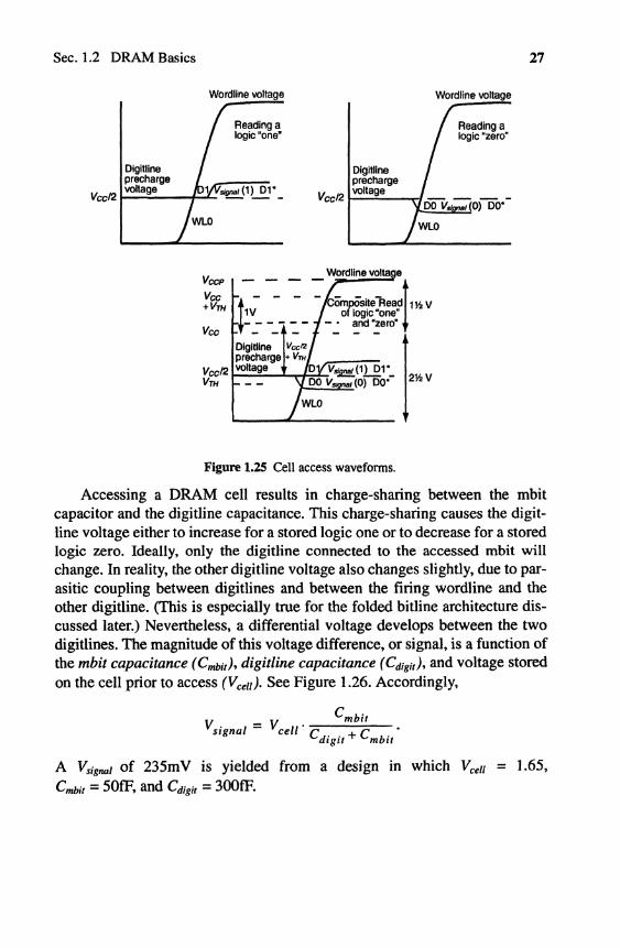
Accessing a DRAM cell results in charge-sharing between the mbitcapacitor and the digitline capacitance. This charge-sharing causes the digit-line voltage either to increase for a stored logic one or to decrease for a storedlogic zero. Ideally, only the digitline connected to the accessed mbit willchange. In reality, the other digitline voltage also changes slightly, due to par-asitic coupling between digitlines and between the firing wordline and theother digitline. (This is especially true for the folded bitline architecture dis-cussed later.) Nevertheless, a differential voltage develops between the twodigitlines. The magnitude of this voltage difference, or signal, is a function ofthe mbit capacitance (Cmbit), digitline capacitance (Cdigit), and voltage storedon the cell prior to access (VceU). See Figure 1.26. Accordingly,
Cy _ y mbit
signal ~~ cell' r* . ncdigit + ^mbit
A Vsignai of 235mV is yielded from a design in which Vceu = 1.65,Cmbit = 5OfF, and Cdigit = 3OOfF.

28 Chap. 1 An Introduction to DRAM
After the cell has been accessed, sensing occurs. Sensing is essentiallythe amplification of the digitline signal or the differential voltage betweenthe digitlines. Sensing is necessary to properly read the cell data and refreshthe mbit cells. (The reason for forming a digitline pair now becomes appar-ent.) Figure 1.27 presents a schematic diagram for a simplified sense ampli-fier circuit: a cross-coupled NMOS pair and a cross-coupled PMOS pair.The sense amplifiers also appear like a pair of cross-coupled inverters inwhich ACT and NLAT* provide power and ground. The NMOS pair orNsense-amp has a common node labeled NLAT* (for Nsense-amp latch).
Similarly, the Psense-amp has a common node labeled ACT (for Activepull-up). Initially, NLAT* is biased to Vcc/2, and ACT is biased to VSs orsignal ground. Because the digitline pair Dl and D l * are both initially atV c c / 2 , the Nsense-amp transistors are both OFF. Similarly, both Psense-amp transistors are OFF. Again, when the mbit is accessed, a signal devel-ops across the digitline pair. While one digitline contains charge from thecell access, the other digitline does not but serves as a reference for theSensing operation. The sense amplifiers are generally fired sequentially: theNsense-amp first, then the Psense-amp. Although designs vary at this point,the higher drive of NMOS transistors and better VTH matching offer bettersensing characteristics by Nsense-amps and thus lower error probabilitycompared to Psense-amps.
Waveforms for the Sensing operation are shown in Figure 1.28. TheNsense-amp is fired by bringing NLAT* (N sense-amp latch) towardground. As the voltage difference between NLAT* and the digitlines (Dland D l * in Figure 1.27) approaches VTH, the NMOS transistor whose gateis connected to the higher voltage digitline begins to conduct. This conduc-tion occurs first in the subthreshold and then in the saturation region as thegate-to-source voltage exceeds VTH and causes the low-voltage digitline todischarge toward the NLAT* voltage. Ultimately, NLAT* will reach groundand the digitline will be brought to ground potential. Note that the otherNMOS transistor will not conduct: its gate voltage is derived from the low-
Initially, VCCI2 MOSFET access
f .—initially, V^,
/T TCapacitance r*? AYccfeofdigitline V O
Figure 1.26 DRAM charge-sharing.

Sec. 1.2 DRAM Basics 29
Psense-amp Nsense-amp• . ' D1
_IY7T¥LACT—i* S<f ^ X <• NLAT*
-ruXn-i-I or
Figure 1.27 Sense amplifier schematic.
voltage digitline, which is being discharged toward ground. In reality, para-sitic coupling between digitlines and limited subthreshold conduction by thesecond transistor result in voltage reduction on the high digitline.
Sometime after the Nsense-amp fires, ACT will be brought toward Vcc
to activate the Psense-amp, which operates in a complementary fashion tothe Nsense-amp. With the low-voltage digitline approaching ground, there isa strong signal to drive the appropriate PMOS transistor into conduction.This conduction, again moving from subthreshold to saturation, charges thehigh-voltage digitline toward ACT, ultimately reaching VCc- Because thembit transistor remains ON, the mbit capacitor is refreshed during the Sens-ing operation. The voltage, and hence charge, which the mbit capacitor heldprior to accessing, is restored to a full level: Vcc for a logic one and groundfor a logic zero. It should be apparent now why the minimum wordline volt-age is a VTIi above VCc- If VCCP
w ^ r e anything less, a full VCc level could notbe written back into the mbit capacitor. The mbit transistor source voltageVsource cannot be greater than Vgate- VTH because this would turn OFF thetransistor.
VCCP — — •— * —
/wLO
/ ACT / /D1
/ NLAT*\j^^
Figure 1.28 Sensing operation waveforms.

30 Chap. 1 An Introduction to DRAM
1.2.2 Write Operation
A Write operation is similar to a Sensing and Restore operation exceptthat a separate Write driver circuit determines the data that is placed into thecell. The Write driver circuit is generally a tristate inverter connected to thedigitlines through a second pair of pass transistors, as shown in Figure 1.29.These pass transistors are referred to as I/O transistors. The gate terminalsof the I/O transistors are connected to a common column select (CSEL) sig-nal. The CSEL signal is decoded from the column address to select whichpair (or multiple pairs) of digitlines is routed to the output pad or, in thiscase, the Write driver.
In most current DRAM designs, the Write driver simply overdrives thesense amplifiers, which remain ON during the Write operation. After thenew data is written into the sense amplifiers, the amplifiers finish the Writecycle by restoring the digitlines to full rail-to-rail voltages. An example isshown in Figure 1.30 in which Dl is initially HIGH after the Sensing opera-tion and LOW after the writing operation. A Write operation usuallyinvolves only 2-4 mbits within an array of mbits because a single CSEL lineis generally connected to only four pairs of I/O transistors. The remainingdigitlines are accessed through additional CSEL lines that correspond to dif-ferent column address locations.
Write driver
H>-fe—1
ENABLE
I/O transistors
1 —r~—D1
ACT-i> S<" p x f i>—NLAr
,J"T_ I—n i . 1 n -i i Dr
i cSEL
I/O I/O*
Figure 1.29 Sense amplifier schematic with I/O devices.

Figure 1.30 Write operation waveforms.
1.2.3 Opening a Row (Summary)
Opening a row of mbits in a DRAM array is a fundamental operation forboth reading and writing to the DRAM array. Sometimes the chain of eventsfrom a circuit designer's point of view, which lead to an open row, is calledthe RAS timing chain. We summarize the RAS timing chain of events below,assuming that for a second-generation DRAM both RAS and CAS are HIGH.(It's trivial to extend our discussion to third-generation DRAMs where RASand CAS are effectively generated from the control logic.)
1. Initially, both RAS and CAS are HIGH. All bitlines in the DRAM aredriven to V c c /2 , while all wordlines are at 0 V. This ensures that all ofthe mbit's access transistors in the DRAM are OFF.
2. A valid row address is applied to the DRAM and RAS goes LOW.While the row address is being latched, on the falling edge of RAS,and decoded, the bitlines are disconnected from the Vcc/2 bias andallowed to float. The bitlines at this point are charged to VCc^ andthey can be thought of as capacitors.
3. The row address is decoded and applied to the wordline drivers. Thisforces only one rowline in at least one memory array to VCCP- Drivingthe wordline to VCCP turns ON the mbits attached to this rowline andcauses charge-sharing between the mbit capacitance and the capaci-tance of the corresponding bitline. The result is a small perturbation(upwards for a logic one and downwards for a logic zero) in the bitlinevoltages.
Sec. 1.2 DRAM Basics 31
VCCP 4- i
/wLO
I CSEL &/ ENABLE
Vcc . . . i . . . \ , • •
//vMr \ 7\ / ,'ov \
•+ ». «4 • ~+ • - ^ •Access Sense Write Restore

32 Chap. 1 An Introduction to DRAM
4. The next operation is Sensing, which has two purposes: (a) to deter-mine if a logic one or zero was written to the cell and (b) to refreshthe contents of the cell by restoring a full logic zero (0 V) or one(VCc) to the capacitor. Following the wordlines going HIGH, theNsense-amp is fired by driving, via an n-channel MOSFET, NLAT*to ground. The inputs to the sense amplifier are two bitlines: the bit-line we are sensing and the bitline that is not active (a bitline that isstill charged to VCc/2—an inactive bitline). Pulling NLAT* to groundresults in one of the bitlines going to ground. Next, the ACT signal ispulled up to VCc, driving the other bitline to VCc- Some importantnotes:
(a) It doesn't matter if a logic one or logic zero was sensed becausethe inactive and active bitlines are pulled in opposite directions.
(b) The contents of the active cell, after opening a row, are restoredto full voltage levels (either 0 V or Vcc)- The entire DRAM canbe refreshed by opening each row.
Now that the row is open, we can write to or read from the DRAM. Ineither case, it is a simple matter of steering data to or from the activearray(s) using the column decoder. When writing to the array, buffers set thenew logic voltage levels on the bitlines. The row is still open because thewordline remains HIGH. (The row stays open as long as RAS is LOW.)
When reading data out of the DRAM, the values sitting on the bitlinesare transmitted to the output buffers via the I/O MOSFETs. To increase thespeed of the reading operation, this data, in most situations, is transmitted tothe output buffer (sometimes called a DQ buffer) either through a helperflip-flop or another sense amplifier.
A note is in order here regarding the word size stored in or read out ofthe memory array. We may have 512 active bitlines when a single rowline inan array goes HIGH (keeping in mind once again that only one wordline inan array can go HIGH at any given time). This literally means that we couldhave a word size of 512 bits from the active array. The inherent wide wordsize has led to the push, at the time of this writing, of embedding DRAMwith a processor (for example, graphics or data). The wide word size andthe fact that the word doesn't have to be transmitted off-chip can result inlower-power, higher-speed systems. (Because the memory and processordon't need to communicate off-chip, there is no need for power-hungry,high-speed buffers.)

Sec. 1.2 DRAM Basics 33
1.2.4 Open/Folded DRAM Array Architectures
Throughout the book, we make a distinction between the open arrayarchitecture as shown in Figures 1.22 and 1.24 and the folded DRAM arrayused in modern DRAMs and seen in Figure 1.31. At the cost of increasedlayout area, folded arrays increase noise immunity by moving sense ampinputs next to each other. These sense amp inputs come directly from theDRAM array. The term folded comes from taking the DRAM arrays seen inFigure 1.24 and folding them together to form the topology seen in Figure1.31.
Figure 1.31 A folded DRAM array.
REFERENCES
[1] R. J. Baker, H. W. Li, and D. E. Boyce, CMOS: Circuit Design, Layout, andSimulation. Piscataway, NJ: IEEE Press, 1998.
[2] Micron Technology, Inc., Synchronous DRAM Data Sheet, 1999.
FOR FURTHER REFERENCE
See the Appendix for additional readings and references.
WLO WL1 WL2 WL3
1 I ., \DV
Sense ampAAAA