an etch hole-free process for temperature …
TRANSCRIPT
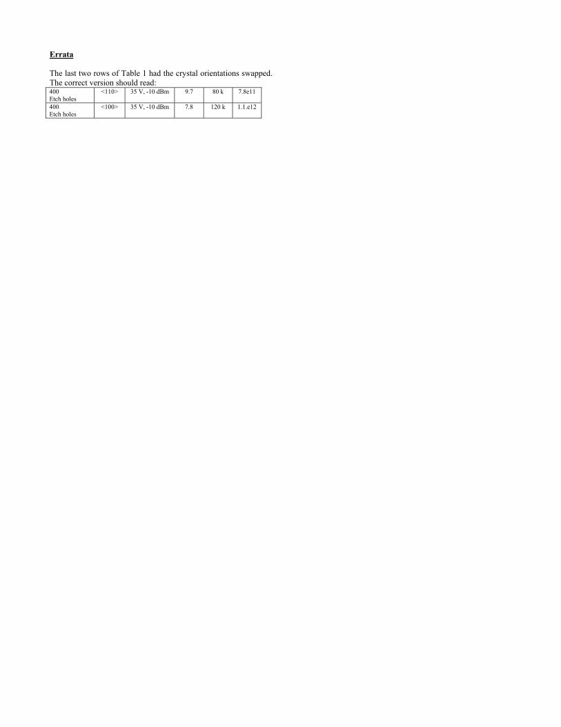
(a) (b) Figure 2. 45° SEM images of an encapsulated device free from etch perforations, from (a) the top side and (b) the underside.
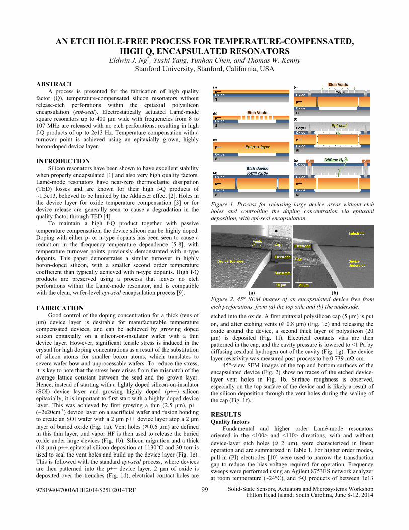
Figure 1. Process for releasing large device areas without etchholes and controlling the doping concentration via epitaxialdeposition, with epi-seal encapsulation.
AN ETCH HOLE-FREE PROCESS FOR TEMPERATURE-COMPENSATED, HIGH Q, ENCAPSULATED RESONATORS
Eldwin J. Ng*, Yushi Yang, Yunhan Chen, and Thomas W. Kenny Stanford University, Stanford, California, USA
ABSTRACT
A process is presented for the fabrication of high quality factor (Q), temperature-compensated silicon resonators without release-etch perforations within the epitaxial polysilicon encapsulation (epi-seal). Electrostatically actuated Lamé-mode square resonators up to 400 μm wide with frequencies from 8 to 107 MHz are released with no etch perforations, resulting in high f-Q products of up to 2e13 Hz. Temperature compensation with a turnover point is achieved using an epitaxially grown, highly boron-doped device layer.
INTRODUCTION
Silicon resonators have been shown to have excellent stability when properly encapsulated [1] and also very high quality factors. Lamé-mode resonators have near-zero thermoelastic dissipation (TED) losses and are known for their high f-Q products of ~1.5e13, believed to be limited by the Akhieser effect [2]. Holes in the device layer for oxide temperature compensation [3] or for device release are generally seen to cause a degradation in the quality factor through TED [4].
To maintain a high f-Q product together with passive temperature compensation, the device silicon can be highly doped. Doping with either p- or n-type dopants has been seen to cause a reduction in the frequency-temperature dependence [5-8], with temperature turnover points previously demonstrated with n-type dopants. This paper demonstrates a similar turnover in highly boron-doped silicon, with a smaller second order temperature coefficient than typically achieved with n-type dopants. High f-Q products are preserved using a process that leaves no etch perforations within the Lamé-mode resonator, and is compatible with the clean, wafer-level epi-seal encapsulation process [9]. FABRICATION
Good control of the doping concentration for a thick (tens of μm) device layer is desirable for manufacturable temperature compensated devices, and can be achieved by growing doped silicon epitaxially on a silicon-on-insulator wafer with a thin device layer. However, significant tensile stress is induced in the crystal for high doping concentrations as a result of the substitution of silicon atoms for smaller boron atoms, which translates to severe wafer bow and unprocessable wafers. To reduce the stress, it is key to note that the stress here arises from the mismatch of the average lattice constant between the seed and the grown layer. Hence, instead of starting with a lightly doped silicon-on-insulator (SOI) device layer and growing highly doped (p++) silicon epitaxially, it is important to first start with a highly doped device layer. This was achieved by first growing a thin (2.5 μm), p++ (~2e20cm-3) device layer on a sacrificial wafer and fusion bonding to create an SOI wafer with a 2 μm p++ device layer atop a 2 μm layer of buried oxide (Fig. 1a). Vent holes (⌀0.6 μm) are defined in this thin layer, and vapor HF is then used to release the buried oxide under large devices (Fig. 1b). Silicon migration and a thick (18 μm) p++ epitaxial silicon deposition at 1130°C and 30 torr is used to seal the vent holes and build up the device layer (Fig. 1c). This is followed with the standard epi-seal process, where devices are then patterned into the p++ device layer. 2 μm of oxide is deposited over the trenches (Fig. 1d), electrical contact holes are
etched into the oxide. A first epitaxial polysilicon cap (5 μm) is put on, and after etching vents (⌀0.8 μm) (Fig. 1e) and releasing the oxide around the device, a second thick layer of polysilicon (20 μm) is deposited (Fig. 1f). Electrical contacts vias are then patterned in the cap, and the cavity pressure is lowered to <1 Pa by diffusing residual hydrogen out of the cavity (Fig. 1g). The device layer resistivity was measured post-process to be 0.739 mΩ-cm.
45°-view SEM images of the top and bottom surfaces of the encapsulated device (Fig. 2) show no traces of the etched device-layer vent holes in Fig. 1b. Surface roughness is observed, especially on the top surface of the device and is likely a result of the silicon deposition through the vent holes during the sealing of the cap (Fig. 1f).
RESULTS Quality factors
Fundamental and higher order Lamé-mode resonators oriented in the <100> and <110> directions, with and without device-layer etch holes (⌀ 2 μm), were characterized in linear operation and are summarized in Table 1. For higher order modes, pull-in (PI) electrodes [10] were used to narrow the transduction gap to reduce the bias voltage required for operation. Frequency sweeps were performed using an Agilent 8753ES network analyzer at room temperature (~24°C), and f-Q products of between 1e13
9781940470016/HH2014/$25©2014TRF 99 Solid-State Sensors, Actuators and Microsystems WorkshopHilton Head Island, South Carolina, June 8-12, 2014

Figure 4. Frequency-temperature dependence of highly boron-doped Lamé resonators with fitted temperature coefficients.
Table 1: Lamé-mode resonator designs and test results.
Edge length (μm), design features
Crystal Orientation
Bias voltage, input power
Frequency (MHz)
Quality Factor
f-Q (Hz)
400 <100> 15 V, -15 dBm 8.1 1.7 M 1.4e13 400 <110> 15 V, -15 dBm 10.0 1.7 M 1.7e13 300 Pull-in <110> 30 V, -40 dBm 13.4 1.2 M 1.6e13 250 <100> 25 V, -15 dBm 13.0 1.5 M 2.0 e13 250 <110> 35 V, -15 dBm 16.1 1.0 M 1.6e13 300 Pull-in (3rd order)
<110> 35 V, -15 dBm 40.3 370 k 1.5e13
300 Pull-in (4th order)
<110> 35 V, -15 dBm 53.7 380 k 2.0e13
300 Pull-in (8th order)
<110> 70 V, -15 dBm 107.3 100 k 1.1e13
400 Etch holes
<100> 35 V, -10 dBm 9.7 80 k 7.8e11
400 Etch holes
<110> 35 V, -10 dBm 7.8 120 k 1.1.e12
(a) (b)
Figure 3. (a) 4th order resonant Lamé mode shape in the <110>direction with 300 μm edge length, actuated using pull-inelectrodes. (b) Frequency sweep with an f-Q product of 2.0e13 Hz.
and 2e13 Hz were consistently observed for the resonators without etch holes. A frequency sweep of the 4th order Lamé mode is shown in Fig. 3. This f-Q of 2.0e13 Hz is about three times as high as achieved in the epi-seal process with limited release areas [11]. Temperature Compensation
It is seen that highly boron-doped Lamé resonators in the <100> and <110> directions show different frequency-temperature dependences (Fig. 4). Notably, the <110> Lamé resonators have temperature turnover points, with smaller second order temperature coefficients of ~-22 ppb/°C2 as compared to the typical -65 ppb/°C2 for temperature-compensated n-type resonators [12].
CONCLUSION
Demonstrated is a process for achieving high quality factor resonators in conjunction with temperature-compensation within an ultra-clean encapsulation process. No residual etch holes are present in the device, allowing for high quality factors. For temperature compensation, epitaxial deposition was used to achieve good control of the device boron doping. Stress effects from the high dopant concentration are mitigated by starting with a highly doped seed. Resonators with f-Q products of up to 2.0e13 Hz are demonstrated with temperature turnover points.
ACKNOWLEDGEMENTS This work was supported by DARPA grant N66001-12-1-4260, “Precision Navigation and Timing program (PNT),” managed by Dr. Robert Lutwak, and DARPA grant FA8650-13-1-7301, “Mesodynamic Architectures (MESO),” managed by Dr. Jeff Rogers. The fabrication work was performed at the Stanford Nanofabrication Facility (SNF) which is supported by National Science Foundation through the NNIN under Grant ECS-9731293.
REFERENCES [1] B. Kim et al., "Frequency Stability of Wafer-Scale Film
Encapsulated Silicon Based MEMS Resonators," Sensors and Actuators A, vol. 136, pp. 125-131, May 2007.
[2] S. A. Chandorkar et al., "Limits of Quality Factor in Bulk-Mode Micromechanical Resonators," IEEE MEMS 2008, pp. 74-77, 2008.
[3] V. Thakar and M. Rais-Zadeh, "Temperature-compensated Piezoelectrically Actuated Lamé-mode Resonators," IEEE MEMS 2014, pp. 214-217, Jan 2014.
[4] C. Tu and J. E.-Y. Lee, "Study on Thermoelastic Dissipation in Bulk Mode Resonators with Etch Holes," IEEE NEMS 2012, pp. 478-482, 2012.
[5] J. S. Wang, K. M. Lakin, and A. R. Landin, "Sputtered C-Axis Inclined Piezoelectric Films and Shear Wave Resonators," IEEE Freq. Ctrl. Sym. 1983, pp. 144-150, 1983.
[6] A. K. Samarao and F. Ayazi, "Temperature Compensation of Silicon Micromechanical Resonators via Degenerate Doping," IEEE IEDM 2009, pp. 737-740, 2009.
[7] M. Shahmohammadi, B. P. Harrington, and R. Abdolvand, "Turnover Temperature Point in Extensional-Mode Highly Doped Silicon Microresonators," IEEE Trans. Elec. Dev., vol. 60, pp. 1213-1220, Mar 2013.
[8] T. Pensala, A. Jaakkola, M. Prunnila, and J. Dekker, "Temperature Compensation of Silicon MEMS Resonators by Heavy Doping," IEEE Intl. Ultrasonics Symposium 2011, pp. 1952-1955, 2011.
[9] R. N. Candler et al., "Long-Term and Accelerated Life Testing of a Novel Single-Wafer Vacuum Encapsulation for MEMS Resonators," JMEMS, vol. 15, pp. 1446-1456, Dec 2006.
[10] E. J. Ng et al., "Stable Pull-in Electrodes for Narrow Gap Actuation," IEEE MEMS 2014, pp. 1281-1284, 2014.
[11] R. Melamud et al., "MEMS Enables Oscillators with sub-ppm Frequency Stability and sub-ps Jitter," Hilton Head 2012, pp. 66-69, 2012.
[12] A. Jaakkola, M. Prunnila, T. Pensala, J. Dekker, and P. Pekko, "Determination of Doping and Temperature Dependent Elastic Constants of Degenerately Doped Silicon from MEMS Resonators," arXiv: 1401.1363 [cond-mat.mtrl-sci], 2014.
CONTACT *E.J. Ng; [email protected]
100
Errata The last two rows of Table 1 had the crystal orientations swapped. The correct version should read:
400 Etch holes
<110> 35 V, -10 dBm 9.7 80 k 7.8e11
400 Etch holes
<100> 35 V, -10 dBm 7.8 120 k 1.1.e12