an estimation method for gate delay variability in
TRANSCRIPT

1
UNIVERSIDADE FEDERAL DO RIO GRANDE DO SUL
PROGRAMA DE PÓS-GRADUAÇÃO EM MICROELETRÔNICA
DIGEORGIA NATALIE DA SILVA
An Estimation Method for Gate DelayVariability in Nanometer CMOS Technology
Thesis presented in partial fulfillment of therequirements for the degree of Doctor inMicroelectronics.
Prof. Dr. Renato Perez RibasAdvisor
Prof. Dr. André ReisCo-advisor
Porto Alegre, August 2010.

2
CIP – CATALOGAÇÃO NA PUBLICAÇÃO
UNIVERSIDADE FEDERAL DO RIO GRANDE DO SULReitor: Prof. Carlos Alexandre NettoVice-Reitor: Prof. Rui Vicente OppermannPró-Reitor de Pós-Graduação: Prof. Aldo Bolten LucionDiretor do Instituto de Informática: Prof. Flávio Rech WagnerCoordenador do PPGC: Prof. Álvaro Freitas MoreiraBibliotecária-Chefe do Instituto de Informática: Beatriz Regina Bastos Haro

3
ACKNOWLEDGEMENTS
I would like to thank my advisor, Prof. Renato Perez Ribas, who guided methroughout my PhD thesis work and provided me with the opportunity to work on avery important topic in Microelectronics. Also, I thank Professor André Inácio Reis forhis precious suggestions and support. I am thankful to Prof. Sachin Sapatnekar forreceiving me at the University of Minnesota and teaching me an important backgroundto be used in my research.
I’m grateful to my laboratory colleagues and friends Carlos Klock, Diogo Silva,Felipe Marques, Nívea Schuch, Pedro Paganela, Rafael da Silva, Vinicius Callegaro,Vinicius Dal Bem, and especially Caio Alegretti, Paulo Butzen and Oswaldo Martinellofor their company and their help with discussions that enriched my work. Also, I wouldlike to thank Alessandro Goulart for all his assistance and Leomar da Rosa Júnior forhis precious advices and talks when I first got into the group.
To my other colleagues and friends at UFRGS, Adriel Zsiemer, Cristina Meinhardt,Edgar Correa, Felipe Pinto, Giovani Pesenti, Glauco Valim, Guilherme Flach, GustavoWilke and Tatiana Marcondes, I’d like to say that it would be very hard to go throughall this journey without the friendship and the amazing moments you guys provided mewith.
I specially thank Lucas Brusamarello, a very important person in my life, for being aloyal friend and the best company ever.
I thank my godmothers, Francisca and Escolástica, and my father, Geraldo Ramos,for their love and support. I thank my brother, Dangelis, for being so helpful,compassionate, loyal and supportive. Finally, I thank my mother, Olita Ferreira, for herendless love and admirable example.

4
To my brother
5
TABLE OF CONTENTS
LIST OF ABREVIATIONS........................................................................................... 8LIST OF FIGURES........................................................................................................ 9LIST OF TABLES........................................................................................................ 12RESUMO....................................................................................................................... 14ABSTRACT .................................................................................................................. 151 INTRODUCTION ................................................................................................ 162 DIGITAL DESIGN AND PARAMETER VARIABILITY IN INTEGRATEDCIRCUITS..................................................................................................................... 182.1 Digital Integrated Circuit Design.................................................................... 182.1.1 Logic Styles ................................................................................................ 202.1.2 Logic Gates with Pull-up and Pull-down Networks................................... 202.1.3 Cascode Voltage Switch Logic................................................................... 222.1.4 Pass-Transistor Logic ................................................................................. 222.1.5 Logic Functions and Transistor Networks................................................. 222.1.6 Standard Cell Design Flow......................................................................... 232.2 Variability in Integrated Circuits ................................................................... 242.2.1 Sources of Process Variations .................................................................... 242.2.1.1 Photolithography ................................................................................................ 242.2.1.2 Etch..................................................................................................................... 252.2.1.3 Line Edge Roughness (LER).............................................................................. 252.2.1.4 Chemical Mechanical Polishing (CMP)............................................................. 252.2.1.5 Random Dopant Fluctuations (RDF).................................................................. 262.2.2 Variability of Process Parameters............................................................... 262.2.2.1 Variability of Gate Length.................................................................................. 262.2.2.2 Variability of Thin Film Thickness .................................................................... 262.2.2.3 Variability of Interconnect and Dielectric .......................................................... 262.2.3 Variability of Device Characteristics ......................................................... 272.2.4 Physical Variability Due to Aging and Wearout ........................................ 272.2.5 Environmental Variations........................................................................... 272.2.6 Variations due to Modeling ........................................................................ 272.2.7 Typical Values for the Parameter Variations ............................................. 282.2.8 Spatial Scales of Variations........................................................................ 282.2.8.1 Global Variations................................................................................................ 282.2.8.2 Local Variations ................................................................................................. 282.2.8.3 Spatially Correlated Variations .......................................................................... 292.2.8.4 Independent Variations....................................................................................... 292.2.9 Parametric Yield ......................................................................................... 292.2.10 Considerations ............................................................................................ 31

6
2.3 Analysis of the Impact of Parameter Variation on the Threshold VoltageVariation........................................................................................................................ 322.3.1 Variations due to Random-Dopant Fluctuations, Channel Length and OxideThickness Variations ...................................................................................................... 323 TIMING ANALYSIS ........................................................................................... 363.1 Critical Path Method (CPM)........................................................................... 363.2 Statistical Concepts........................................................................................... 373.3 Statistical Static Timing Analysis (SSTA)...................................................... 393.4 SSTA Solution Approaches ............................................................................. 393.4.1 Numerical Integration Method ................................................................... 393.4.2 Monte-Carlo Method .................................................................................. 393.4.3 Probabilistic Analysis Methods .................................................................. 403.5 Delay Modeling ................................................................................................. 403.5.1 Introduction ................................................................................................ 403.5.1.1 Delay................................................................................................................... 413.5.1.2 Transition Time .................................................................................................. 413.5.2 Gate and Interconnect Timing Models ....................................................... 413.5.3 Elmore Delay Model .................................................................................. 423.5.3.1 RC Tree............................................................................................................... 423.5.4 Asymptotic Waveform Evaluation (AWE) ................................................ 433.6 Process Variation Modeling............................................................................. 463.6.1 Statistical Delay Models............................................................................. 463.6.2 Pelgrom Model ........................................................................................... 474 PROPOSAL AND METHODOLOGY............................................................... 494.1 Introduction ...................................................................................................... 494.2 Motivation ......................................................................................................... 494.3 Proposal ............................................................................................................. 514.4 Methodology...................................................................................................... 515 CMOS LOGIC GATE PERFORMANCE VARIABILITY............................. 545.1 Introduction ...................................................................................................... 545.2 Variability of Different Transistors Networks............................................... 545.2.1 Pull-down Network..................................................................................... 555.2.2 Pull-up Network ......................................................................................... 565.3 CMOS Inverter ................................................................................................. 565.3.1 Analysis ...................................................................................................... 575.3.2 Inverter Sizing ............................................................................................ 575.3.3 Output Load................................................................................................ 605.3.4 Input Transition Time................................................................................. 615.3.5 Transistor Network Arrangements ............................................................. 625.4 NAND and NOR Gates..................................................................................... 655.5 NAND: Single Gate Versus Mapped Circuit ................................................. 685.6 And-Or-Inverter (AOI) Logic Gates............................................................... 705.7 Conclusion ......................................................................................................... 726 VARIABILITY ESTIMATION METHOD....................................................... 736.1 On-Resistance.................................................................................................... 756.1.1 Response Surface Methodology ................................................................. 766.2 MOS Structures Capacitances ........................................................................ 776.2.1 Gate Capacitance ........................................................................................ 786.2.1.1 Channel Capacitance .......................................................................................... 78
7
6.2.1.2 Overlap Capacitance........................................................................................... 786.2.2 Junction Capacitances................................................................................. 796.2.2.1 Bottom-Plate Junction Capacitance.................................................................... 796.2.2.2 Side-Wall Junction Capacitance......................................................................... 806.2.3 The Inverter ................................................................................................ 806.3 Modeling the Falling-Edge Delay Deviation of a NAND3............................. 817 MODELING THE DELAY VARIABILITY OF TRANSISTOR NETWORKS.......... .............................................................................................................................. 837.1 Calculation of Resistances ............................................................................... 837.2 Resistance of Parallel Transistors ................................................................... 847.3 Resistance of Series Transistors ...................................................................... 857.4 Estimation of Performance Deviation............................................................. 867.4.1 Series Networks.......................................................................................... 877.4.2 Parallel Networks ....................................................................................... 897.4.3 Delay Variability Estimation Method Considering the Saturated Region ofOperation ................................................................................................................... 907.4.4 Estimation Method Applied to Different Inverter Topologies ................... 927.4.5 The Influence of the Sizing of Transistors on Delay Variability ............... 937.4.6 The Influence of the Output Load on Delay Variability ........................... 957.4.6.1 The Series Transistors Networks........................................................................ 957.4.7 Inverter Chains ........................................................................................... 977.5 Conclusion ......................................................................................................... 988 EVALUATION OF THE PROPOSED DELAY VARIABILITY MODEL ... 998.1 2-Input XOR Logic Gate.................................................................................. 998.2 4-Input XOR Logic Gate................................................................................ 1068.3 Full Adder ....................................................................................................... 1128.4 Complex Gate.................................................................................................. 1168.5 Delay Equation Method ................................................................................. 1178.6 Runtime Analysis............................................................................................ 1188.7 Conclusion ....................................................................................................... 1209 CONCLUSION ..................................................................................................................121REFERENCES ........................................................................................................... 123APPENDIX A RESISTANCE EQUATIONS SCRIPT ......................................... 128APPENDIX B DELAY CALCULATION SCRIPT ............................................... 130APPENDIX C DELAY EQUATION SCRIPT ........................................................ 134APPENDIX D RESUMO DA TESE EM PORTUGUÊS....................................... 135

8
LIST OF ABREVIATIONS
ASIC Application-Specific Integrated Circuits
AWE Asymptotic Waveform Evaluation
BDD Binary Decision Diagram
CAD Computer-Aided Design
CMOS Complementary Metal Oxide Semiconductor
CSP Complementary Series-Parallel
CVSL Cascode Voltage Switch Logic
DCVSL Differential Cascode Voltage Switch Logic
DEM Delay Equation Method
DPTL Differential Pass Transistor Logic
IC Integrated Circuit
MOSFET Metal Oxide Semiconductor Field Effect Transistor
NCSP Non-Complementary Series-Parallel
PDF Probability Density Function
PTL Pass Transistor Logic
PTM Predictive Technology Model
RSM Response Surface Methodology
SSTA Statistical Static Timing Analysis
STA Static Timing Analysis

9
LIST OF FIGURES
Figure 2.1: Design abstraction levels in digital circuits. ................................................ 19Figure 2.2: Complementary logic gate as a combination of a pull-up and a pull-downnetwork ........................................................................................................................... 21Figure 2.3: Different implementations of a logic function............................................. 21Figure 2.4: Basic principle of the Cascode Voltage Switch Logic style ........................ 22Figure 2.5: Pass-transistor implementation of an AND gate.......................................... 22Figure 2.6: Digital circuit design methodology using predefined cell library................ 24Figure 2.7: Leakage current and frequency measured in a sample of 1000 chips.......... 29Figure 2.8: Yield window for frequency constraint of fmin=0.9 fnom and powerconstraint of Pmax = 1.05 Pnom, for negligible static (leakage) power ............................ 30Figure 2.9: Yield window for frequency constraint of fmin=0.9 fnom and powerconstraint of Pmax = 1.05 Pnom, for static (leakage) power .............................................. 31Figure 2.10: Threshold voltage PDFs of NMOS for process parameter variations ....... 34Figure 2.11: Threshold voltage PDFs of PMOS for process parameter variations ........ 35Figure 3.1: An example of a circuit and its timing graph............................................... 36Figure 3.2: Normal distribution of a random variable.................................................... 38Figure 3.3: Gate and interconnect delays represented as probability density functions 40Figure 3.4: The 50% delay and transition time of a waveform ...................................... 41Figure 3.5: A step response e(t) and its derivative ......................................................... 42Figure 3.6: An example of an RC tree............................................................................ 43Figure 3.7: RC system .................................................................................................... 44Figure 3.8: Current-based circuit model for a logic cell................................................. 46Figure 3.9: Representation of transistors that lie on th x-axis ....................................... 48Figure 5.1: Some of the CMOS logic gates used for the analysis of falling-edge delayvariability in relation to the transistor network arrangement ......................................... 55Figure 5.2: Some of the CMOS logic gates used for the analysis of rising-edge delayvariability in relation to the transistor network arrangement ......................................... 56Figure 5.3: Design for analysis....................................................................................... 57Figure 5.4: Mean subthreshold and maximum currents of an inverter in relation to itsarea.................................................................................................................................. 58Figure 5.5: Normalized current deviations of an inverter ............................................. 58Figure 5.6: Timing metrics of an inverter in relation to its area..................................... 59Figure 5.7: Normalized timing metrics deviation of an inverter .................................... 59Figure 5.8: Timing metrics of an inverter....................................................................... 60Figure 5.9: Normalized timing metrics deviation of an inverter ................................... 61Figure 5.10: Topology using an auxiliary inverter (X1-X5) connected to the input of themain inverter for changing the input slope..................................................................... 61Figure 5.11: Timing metrics of an inverter..................................................................... 62

10
Figure 5.12: Normalized timing metrics deviation of an inverter .................................. 62Figure 5.13: Different topologies of an inverter............................................................. 63Figure 5.14: Folding topology of an inverter ................................................................. 64Figure 5.15: Normalized rise and fall delay deviations in relation to the number ofinputs: NAND and NOR gates ....................................................................................... 66Figure 5.16: Comparison of N- and PMOS transistor stacking in NAND and NOR gatesfor different positions of the switching device ............................................................... 67Figure 5.17: Illustration of a single 3-input NAND gate implemented by using two 2-input NAND gates .......................................................................................................... 68Figure 5.18: PDF of rise delay for a 3-input NAND gate and a circuit performing thesame logic function implemented by using two 2-input NAND gates for the best and theworst delay propagations ................................................................................................ 69Figure 5.19: PDF of rise delay for a AOI-21 and AOI-32 gates implemented by usingbasic CMOS cells and as a single complex gate ............................................................ 71Figure 6.1: Combinations of min and max values considered for the threshold voltages(coded variables) of devices in a 3-transistors network ................................................. 74Figure 6.2: Delay variability model methodology.......................................................... 74Figure 6.3: Intrinsic capacitances of a MOS transistor .................................................. 77Figure 6.4: CMOS Inverter............................................................................................. 80Figure 6.5: Switch models of CMOS inverter. ............................................................... 80Figure 6.6: Pull-down network of a 3-input NAND....................................................... 81Figure 7.1: NMOS transistors stacking .......................................................................... 83Figure 7.2: Probability density functions (PDF) of the resistances that constitute modelsfor the transistors in a NMOS series network................................................................. 84Figure 7.3: PMOS transistors stacking........................................................................... 86Figure 7.4: Simulated and fitted curves for rising-edge delay deviation in relation to theoutput load of a 4-stacking PMOS. ................................................................................ 95Figure 7.5: Modeled and fitted curves for falling-edge delay deviation in relation to theoutput load of a 4-stacking NMOS using Elmore Delay model..................................... 96Figure 7.6: Simulated points for falling-edge delay deviation in relation to the outputload of a 4-stacking NMOS. ........................................................................................... 96Figure 7.7: Modeled and fitted curves for falling-edge delay deviation in relation to theoutput load of a 4-stacking NMOS using AWE. ............................................................ 97Figure 7.8: Measurements structures.............................................................................. 97Figure 8.1: 2-input XOR implemented in different logic styles and topologies ............ 99Figure 8.2: PDF of the rising-edge delay for the complex gate implementation of a 2-input XOR .................................................................................................................... 102Figure 8.3: PDF of the rising-edge delay for the implementation of a 2-input XOR withNAND gates ................................................................................................................. 102Figure 8.4: PDF of the rising-edge delay for the PTL implementation of a 2-input XOR...................................................................................................................................... 103Figure 8.5: PDF of rising-edge delay for different implementations of a 2-input XOR...................................................................................................................................... 103Figure 8.6: PDF of the falling-edge delay for the complex gate implementation of a 2-input XOR .................................................................................................................... 104Figure 8.7: PDF of the falling-edge delay for the implementation of a 2-input XOR withNAND gates ................................................................................................................. 104Figure 8.8: PDF of the falling-edge delay for the PTL implementation of a 2-input XOR...................................................................................................................................... 105

11
Figure 8.9: PDF of the falling-edge delay for different implementations of a 2-inputXOR.............................................................................................................................. 105Figure 8.10: 4-input XOR implemented in different logic styles and topologies ........ 106Figure 8.11: PDF of the rising-edge delay for the DCVSL implementation of a 4-inputXOR.............................................................................................................................. 108Figure 8.12: PDF of the rising-edge delay for the DPTL implementation of a 4-inputXOR.............................................................................................................................. 108Figure 8.13: PDF of rising-edge delay for different implementations of a 4-input XOR...................................................................................................................................... 109Figure 8.14: PDF of the falling-edge delay for the DCVSL implementation of a 4-inputXOR.............................................................................................................................. 110Figure 8.15: PDF of the falling-edge delay for the DPTL implementation of a 4-inputXOR.............................................................................................................................. 110Figure 8.16: PDF of falling-edge delay for different implementations of a 4-input XOR...................................................................................................................................... 111Figure 8.17: PDF of falling-edge delay for DPTL implementation of a 4-input XORmodeled with AWE technique...................................................................................... 112Figure 8.18: Full Adder implemented in different logic styles .................................... 113Figure 8.19: "SUM" output node PDF of the rising-edge delay for differentimplementations of a full adder .................................................................................... 115Figure 8.20: "SUM" output node PDF of the falling-edge delay for differentimplementations of a full adder .................................................................................. 115Figure 8.21: A complex gate implementation .............................................................. 116Figure 8.22: PDF of the rising-edge delay for the complex gate implementation ....... 117Figure 8.23: PDF of the rising-edge delay for the complex gate implementation ....... 117

12
LIST OF TABLES
Table 2.1: 3σ Variation points for the technology parameters of a typical 0.18 µmCMOS process................................................................................................................ 28Table 2.2: VTH deviation according to variations in the channel length, oxide thicknessand RDF for NMOS and PMOS transistors ................................................................... 35Table 5.1: Normalized fall delay deviations for different topologies............................. 55Table 5.2: Normalized rise delay deviations for different topologies ............................ 56Table 5.3: Subthreshold leakage current values for the inverter topologies .................. 63Table 5.4: Rise and fall delays for the inverter topologies............................................. 63Table 5.5: Rise and fall transition times for the inverter topologies .............................. 64Table 5.6: Delay deviations for the shortest and the longest paths in Fig. 8.15............ 68Table 5.7: Delay deviations for AOI_21 and AOI_32 logic gates ................................ 70Table 6.1: Combinations of min and max values considered for the threshold voltages(coded variables) of devices in a 3-transistors network. ................................................ 73Table 7.1: Approximate resistance equations for transistors in a parallel network....... 84Table 7.2: Approximate resistance equations for NMOS transistors in a series network......................................................................................................................................... 85Table 7.3: Approximate resistance equations for PMOS transistors in a series network.......................................................................................................................................... 86Table 7.4: Delay deviations for NMOS transistors in a series network, according to theposition of the switching transistor in relation to the output node (1-close...4-far) ...... 87Table 7.5: Delay deviations for PMOS transistors in a series network, according to theposition of the switching transistor in relation to the output node (1-close...4-far) ...... 88Table 7.6: Delay deviations for NMOS transistors in parallel networks, according to thenumber of switching transistors...................................................................................... 89Table 7.7: Delay deviations for PMOS transistors in parallel networks, according to thenumber of switching transistors...................................................................................... 90Table 7.8: Delay deviation for N- and PMOS transistors in series networks, according tothe position of the switching transistor in relation to the output node (1-close...4-far) forthe linear and the saturation region of operation ............................................................ 91Table 7.9: Delay deviation for N- and PMOS transistors in parallel networks, accordingto the number of switching transistor for the linear and the saturation region ofoperation. ........................................................................................................................ 92Table 7.10: Rise and fall delay deviations for different inverter topologies. ................. 92Table 7.11: Rise and fall delay deviations for different inverter topologies with differentthreshold voltage variations............................................................................................ 93Table 7.12: Rise and fall delay deviations for different sizes of inverters ..................... 94

13
Table 7.13: Rise and fall delay deviations for different sizes of inverters with differentthreshold voltage variations............................................................................................ 94Table 7.14: Rise and fall delay deviations for different chains of inverters .................. 98Table 8.1: Delay deviations for different implementations of a 2-input XOR provided bystatistical simulation and by the proposed method....................................................... 100Table 8.2: Delay values and deviations for different implementations of a 2-input XOR...................................................................................................................................... 101Table 8.3: Delay deviations for different implementations of a 4-input XOR provided bystatistical simulation and by the proposed method....................................................... 106Table 8.4: Delay values and deviations for different implementations of a 4-input XOR...................................................................................................................................... 107Table 8.5: Truth table of a full adder............................................................................ 112Table 8.6: Delay deviations for different implementations of a full-adder provided bystatistical simulation and the proposed method............................................................ 113Table 8.7: "SUM" delay deviations for different implementations of a 1-bit full-adder...................................................................................................................................... 114Table 8.8: Delay deviations for a complex gate provided by statistical simulation and bythe proposed method..................................................................................................... 116Table 8.9: Runtime analysis for different implementations of a XOR2....................... 118Table 8.10: Delay and runtime analysis of the complex gate topology by using differentmethods......................................................................................................................... 119Table 8.11: Delay and runtime analysis of a XOR4 implemented with a DCVSLtopology by using different methods ............................................................................ 119
14
RESUMO
No regime em nanoescala da tecnologia VLSI, o desempenho dos circuitos é cadavez mais afetado pelos fenômenos de variabilidade, tais como variações de parâmetrosde processo, ruído da fonte de alimentação, ruído de acoplamento e mudanças detemperatura, entre outros. Variações de fabricação podem levar a diferençassignificativas entre circuitos integrados concebidos e fabricados. Devido à diminuiçãodas dimensões dos componentes, o impacto das variações de dimensão crítica tende aaumentar a cada nova tecnologia, uma vez que as tolerâncias de processo não sofremescalonamento na mesma proporção. Muitos estudos sobre a forma como avariabilidade intrínseca dos processos físicos afeta a funcionalidade e confiabilidade doscircuitos têm sido realizados nos últimos anos. Uma vez que as variações de processo setornam um problema mais significativo devido à agressiva redução da tecnologia, umamudança da análise determinística para a análise estatística de projetos de circuitos podereduzir o conservadorismo e o risco que está presente ao se aplicar a técnica tradicional.
O objetivo deste trabalho é propor um método capaz de predizer a variabilidade noatraso de redes de transistores e portas lógicas sem a necessidade da realização desimulações estatísticas consideradas caras em termos computacionais. Este métodoutiliza o modelo de atraso de Elmore e a técnica de Asymptotic Waveform Evaluation
(AWE), considerando as resistências dos transistores obtidas em função das variaçõesdas tensões de limiar dos transistores no arranjo. Uma pré-caracterização foi realizadaem algumas portas lógicas de acordo com a variabilidade de seu desempenho causadospor variações da tensão de limiar dos transistores a partir de simulações Monte Carlo.Uma vez que existem vários tipos de arranjos de redes de transistores e esses arranjosapresentam um comportamento diferente em termos de atraso, consumo de energia, áreae variabilidade dessas métricas, torna-se muito útil identificar os circuitos nos quais asredes de transistores são menos influenciadas pelas variações em seus parâmetros. Omodelamento da variabilidade do atraso é feita através de 2K simulações DC para a rede“pull-up”, 2N simulações DC para a rede “pull-down” (K e N são os números detransistores de cada rede) e uma simulação transiente para cada porta lógica, o que levaapenas alguns segundos no total. O objetivo de toda a análise é fornecer orientaçõespara a geração de redes lógica ótimas que oferecem baixa sensibilidade às variações deseus parâmetros.
Palavras-Chave: Tecnologia CMOS, variabilidade, atraso, redes de transistores.

15
ABSTRACT
In the nanoscale regime of VLSI technology, circuit performance is increasinglyaffected by variational effects such as process variations, power supply noise, couplingnoise and temperature changes. Manufacturing variations may lead to significantdiscrepancies between designed and fabricated integrated circuits. Due to the shrinkingof design dimensions, the relative impact of critical dimension variations tends toincrease with each new technology generation, since the process tolerances do not scalein the same proportion. Many studies on how the intrinsic variability of physicalprocesses affect the functionality and reliability of the circuits have been done in recentyears. Since the process variations become a more significant problem because of theaggressive technology scaling, a shift from deterministic to statistical analysis for circuitdesigns may reduce the conservatism and risk that is present while applying thetraditional technique.
The purpose of the work is to propose a method that accounts for the deviation in theperformance of transistors networks and logic gates without the need of performingcomputationally costly simulations. The estimation method developed uses the ElmoreDelay model and the Asymptotic Waveform Evaluation (AWE), by considering theresistances of transistors obtained as functions of threshold voltages variations of thetransistors in the arrangement. A pre-characterization was performed in some logicgates according to their performance variability caused by variations in the thresholdvoltage of the transistors by running Monte Carlo simulations. Since there are severalkinds of transistor networks arrangements and they present different behavior in termsof delay, power consumption, area and variability of these metrics, it is very useful toidentify circuits with such arrangements of transistors that are less influenced byvariations in their parameters. The delay variability modeling relies on (2K) DCsimulations for the pull-up network, (2N) DC simulations for the pull-down network (Kand N are the number of transistors in the pull-up and pull-down network, respectively)and on a single transient simulation for each gate, which take only a few secondsaltogether. The goal of the whole analysis is to provide guidelines for the generation ofoptimal logic networks that present low sensitivity to variations in their parameters.
Keywords: MOS transistor, performance variability, transistor network.

16
16
1 INTRODUCTON
The electronics industry transitioned from the era of discrete components to the eraof the integrated circuit (IC) in order to achieve higher quality and reliability throughless components to handle and assemble, and higher yields through smaller miniaturedevices (CHIANG, 2007). The process of yield improvement focused on reducing thenumber of impurities and imperfections which resulted in random effects and loweryields, and on shrinking the design features that resulted in smaller die areas and thusmore dies per wafer.
Any manufacturing process presents a certain degree of variability around thenominal value of the product specifications. This phenomenum is accounted for in thedescription of the product characteristics in the form of a window of acceptablevariation for each of its critical parameters. The aggressive shrinking of MOStechnology causes the intrinsic variability present in its fabrication to increase. Processtolerances do not scale proportionally with the design dimensions, causing the relativeimpact of the critical dimension variations to increase with each new technologygeneration (ARGAWAL, 2007). This scenario demands realistic approaches that areable to predict the impact of parameters variations in the metrics of the circuit.
Since the process variations become a more critical issue, the migration fromdeterministic to statistical analysis of circuit designs may reduce the conservatism ofapplying the traditional worst-case approach. The traditional corner-case techniqueseems as a reasonable way to handle global variations but not local ones. In the case ofperformance of a circuit, a logic gate may become slower for a certain variation andfaster for another, and that might depend on its location on a die. Not only theimportance of the intra-die variations has grown but also the number of processparameters that present considerable variations has also increased (SRIVASTAVA,2005). Such situation requires some changes in the traditional techniques in order tofind a better alternative to their deterministic nature.
Increasing levels of processes variations have a major impact on power consumptionand performance of a design, resulting in parametric yield loss. This problem ispotentialized by the fact that timing has an inverse correlation with leakage power, e.g.a reduction in channel length results in improved performance but also causes anexponential increase in leakage power.
The manufacturing process has been based on optical lithography. The wavelengthin recent and future technologies is bigger than the minimum physical drawndimensions (193 nm), so variability due to lithography has been of increasinglyimportance. Also, classical modeling of the behavior of dopant materials reached theend of its validity and quantum mechanical behavior of material needs to be taken intoaccount. Deterministic corner-based methodologies were replaced by statistical analysis

17
in many situations. Furthermore, the random component of variability which wasstrictly global in nature has a new intra-die component of considerable significance.
Different transistors networks present different electrical characteristics, even if theyrepresent the same logic function (ROSA, 2008). In this sense, the goal of this work isto propose a delay method that takes into account the variability in the threshold voltageof the transistors in a specific network. The first step was to analyze how the variabilityin the parameters affects the metrics of the gates according to (i) their topology(quantity of series and parallel transistors) and (ii) the position of the transistor with atransient input signal in relation to the output node. Electrical simulations of the gateswere performed with HSPICE, a standard circuit simulator that is considered the“golden reference” for electric circuits. An estimation method for the delay variabilitywas proposed and evaluated. We attempted to develop an as-simple-as-possiblevariability aware timing method for different logic gates (inverter, NAND, NOR, XORand full adder) and different arrangements of transistors. The transistors wereapproximated as switches controlled by the input signal applied to the gate terminal andwere described by their intrinsic capacitances and their resistances while on conduction(charging or discharging the load capacitance). The resistances and capacitances arefunctions of the parameters of the transistors. The method includes the use of theElmore Delay model (ELMORE, 1948) and the Asymptotic Waveform Evaluation(AWE) (PILLAGE, 1990), by considering the resistances of transistors obtained asfunctions of threshold voltage variations of transistors in the arrangement. The datacollected through eletrical simulation is compared to the results generated by theproposed method. The results of the analysis may be used to achieve circuitimplementations that present some immunity to variability.
A brief introduction to the context and subject of the work is given in CHAPTER 1.It is followed by a general review on digital circuits, including logic functions and gatestopologies, besides the design flow for ASICs as well as a study on the types andsources of variability, in CHAPTER 2. CHAPTER 3 is dedicated to deterministic andstatistical timing analysis concepts, and also to some timing models proposed in theliterature for transistors and logic gates, along with the basic concepts of the timinganalysis that can make use of those models. The proposal of the work and methodologyused to develope it are explained in CHAPTER 4. Preliminary results extracted bysimulations using the electrical simulator HSPICE are presented and analyzed inCHAPTER 5, including a more complete characterization of an inverter according tothe variability on its parametes. The delay variability estimation method proposed inthis work in order to predict the variability of a cell delay under variations in itsparameters is described in CHAPTER 6. CHAPTER 7 presents the results achieved byusing the proposed method to calculate the delay variability for different transistorsnetworks. CHAPTER 8 shows how reliable is the method when applied to calculate thedelay variability of different topologies that are used to implement the same logicfunction. CHAPTER 9 concludes the work.

18
2 DIGITAL DESIGN AND PARAMETER VARIABILITYIN INTEGRATED CIRCUITS
The rapid scaling of CMOS technology has turned the control of critical deviceparameters into a very difficult task, and drastic variations of process and designparameters have resulted. Variations in the physical, operational or modelingparameters of a device lead to variations in electrical device characteristics, such as thethreshold voltage, drive strengh of transistors, and in the resistance and capacitance ofinterconnects. Finally, variations in electrical characteristics of the components lead tovariations in the performance and power consumption of the circuit.
The first section of this chapter presents some concepts about IC design anddifferent logic families, since the main goal of the work is the modeling and analysis ofhow the delay variability is influenced by the use of different topologies of logic gates.
The second section briefly describes some of the major fabrication steps in MOSprocess flow and presents an overview of IC parameter variability. It also presents someof the most important sources of variations, as well as their effects.
That section is also intended to validate the use of non-correlated variations for thethreshold voltages (VTH) of MOS transistors, what means that each transistor has arandom VTH variation, independently on its position on the die. The impact of channellength (L) and oxide thickness (Tox) variations on threshold voltage were compared tothe effect caused on the same electrical parameter by random-dopant fluctuations(RDF).
2.1 Digital Integrated Circuit DesignIn the beginning of the last century, electronics circuits used large, expensive and
power consuming vacuum tubes. In 1947, the first functioning point contact transistorwas built and soon after that the bipolar junction transistor was developed (WESTE,2005). Early integrated circuits (IC) primarily used bipolar transistors, but the largemajority of the current IC’s are implemented in the Metal Oxide Semiconductor (MOS)technology. An integrated circuit is an electronic system consisting of a number ofminiaturized electronic devices, such as transistors, resistors, capacitors and inductors,fabricated in a monolithic semiconductor substrate (RABAEY, 2005).
The level of integration of chips has been classified as small-scale, medium-scale,large-scale and very-large-scale (VLSI). The million-transistor-per-chip barrier wascrossed in the late 1980s and the handcrafted design once implemented has becomeinappropriate (RABAEY, 2005). Instead of the individualized approach of the earlierdesigns, a circuit is constructed in a hierarchical way: a system, such as a processor, is a

19
collection of modules, which are collections of gates that consists in a certain number oftransistors.
Figure 2.1: Design abstraction levels in digital circuits (RABAEY, 2005).
An integrated circuit can be described in terms of three domains: (i) the behavioral
domain, (ii) the structural domain and (iii) the physical domain. The behavioral domainspecifies how the system works, its function. The structural domain specifies theinterconnection of components required to achieve the behavior that is desired. Thephysical domain specifies how to arrange the components in order to connect them,which in turn allows the required behavior (WESTE, 2005). Digital IC design is usedto produce components such as microprocessors, FPGAs (Field-Programmable Gate-Arrays), memories and digital ASICs (Application-Specific Integrated Circuits).
The advance of the technology for constructing ICs demanded the elaboration ofdesign tools able to reduce the complexity, increase productivity and assure the designera working product. Over the last four decades, Computer Aided Design (CAD) toolshave gradually been adopted for various tasks of the design process. The adoption oftools has influenced how circuits are designed in various ways. In some cases certainrestrictions on what is an acceptable design have to be imposed, so that some tools maybe used. In other cases, new tools allow designs to try on several design alternatives,which was not reasonable before since the design was done manually. Design toolsinclude simulation at the various complexity levels, design verification, layoutgeneration and design synthesis.
The viability of an IC design depends on its application and on economicconsiderations. There is a number of distinct implementation approaches ranging fromhigh-performance, handcrafted to fully programmable, medium-to-low performancedesigns (RABAEY, 2005). Design is based on a tradeoff to achieve adequate results forperformance (speed, power consumption, function, flexibility, robustness), size, time todesign, ease of verification, test generation and testability.
When high-performance is desired, handcrafting the circuit topology and physicaldesign seems to be a reasonable option. In full-custom design the logic and physicalsynthesis attain usually the highest performance and smallest size, making use of themost advanced technologies. It is the most technology dependent design approach, since

20
20
each switch element present in every cell is manually fine-tuned in order to explore allthe performance advantages that a given technology can deliver. The disadvantages offull-custom can include increased manufacturing and design time, and much higher skillrequirements on the part of the design team.
In order to avoid the redesign and reverification of frequently used cells, such asbasic gates, arithmetic and memory modules, designers most often resort to celllibraries. Cell-based design uses a standard cell library as the basic building blocks of achip. These libraries not only contain the layouts, but also provide completedocumentation and characterization of the behavior of the cells. Cell library is a finiteset of logic cells that implements different Boolean functions with different drivestrengths and topologies.
Traditionally, the technology mapping methods rely on static pre-characterizedlibraries aiming delay, area and power optimizations. Each cell in the library is fullycharacterized through many simulations, resulting in a set of accurate information aboutthe behavior of the cell. Usually, standard cells have a fixed height with power andground routed respectively at the top and bottom of the cells. As compared to full-custom design, cell-based design offers much higher productivity since the predesignedcells may be reused many times. The disadvantage is that the constrained nature of thelibrary, especially due to the limited number of cells, reduces the possibility of fine-tuning the design (RABAEY, 2005). The variability on the metrics of a logic cell canalso be used as a constraint for the behavior of the cell in a technology mapping.
2.1.1 Logic Styles
Two classes of logic circuits can be identified: a) combinational circuits and b)sequential circuits. Combinational logic circuits present an output that is related to itscurrent input signals by some Boolean expression at any point in time. Sequential logiccircuits have their outputs as functions of the current input data and also of previousvalues of the input signals. A sequential circuit includes a combinational logic portionand a module that holds the state.
Several circuit styles can be used to implement a given logic function. Logic stylesare basically classified as being dynamic or static topologies. A static topology connectseach gate output to either VDD or GND at every point in time but during the switchingtransient (RABAEY, 2005). A dynamic topology relies on the temporary storage ofsignal values on the capacitance of high-impedance circuit nodes.
2.1.2 Logic Gates with Pull-up and Pull-down Networks
Static Complementary MOS is the most widely used logic style, because itpresents some important characteristics: low sensitivity to noise (robustness), goodperformance, low power consumption, availability in standard cell libraries, amongothers. A static CMOS gate is composed of a pull-up and a pull-down network, alsoreferred to as PUN and PDN, respectively. A PUN connects the output of the circuit toVDD and a PDN connects the output to ground (Fig. 2.2).

21
Figure 2.2 Complementary logic gate as a combination of a pull-up and a pull-downnetwork (RABAEY, 2005).
The CMOS structure is naturally an “inverting” gate that is able to implementfunctions such as NAND and NOR. If a non-inverting Boolean function is desired, itrequires an inverter stage. By using inverters, NANDs and NORs it is possible to haveany logic equation (function) implemented.
A major problem in using the CMOS style is the large number of transistors that isrequired to implement a logic function (2N transistors to implement an N-input logicgate). Another characteristic to be considered is the significant load capacitance sinceeach gate drives two devices (a PMOS and an NMOS) per fan-out (number of digitalinputs that the output of a gate can feed). However, a reduction in the number oftransistors can be achieved by using gates that implement more complex functions.These gates are called “Static CMOS Complex Gates” and are obtained by anassociation of series/parallel transistors.
A minimum number of stacking (series) transistors for the CMOS gate may beachieved by deriving the pull-up and pull-down planes from the best choice ofindividual networks, not necessarily representing complemented topologies. (ROSA,2008) shows an algorithm for generating minimum transistor chain networks byequations that represent a given logic function.
Figure 2.3 Different implementations of a logic function (ROSA, 2008).

22
22
2.1.3 Cascode Voltage Switch Logic
Cascode voltage switch logic (CVSL) uses both true and complementary inputsignals and computes both true and complementary outputs using a pair of NMOS pull-down networks (Fig. 2.4). For any given input pattern, one of the pull-down networkswill be ON and the other OFF. The pull-down network that is ON will pull that outputlow. This low output turns ON the PMOS to pull the opposite output high. When theopposite output rises, the other PMOS turns OFF so no static power dissipation occurs(WESTE, 2005). CVSL increases the speed of the circuit because all of the logic isperformed with NMOS transistors, thus reducing the input capacitance.
Figure 2.4 Basic principle of the Cascode Voltage Switch Logic style (RABAEY,2005).
2.1.4 Pass-Transistor Logic
In pass-transistor logic (PTL), inputs of the circuit are also applied to thesource/drain diffusion terminals in an attempt to reduce the number of transistorsrequired to implement the logic (RABAEY, 2005). These circuits use either NMOSpass transistors or parallel NMOS and PMOS transistors (transmission gates) asswitches (Fig. 2.5).
Figure 2.5 Pass-transistor implementation of an AND gate (RABAEY, 2005).
2.1.5 Logic Functions and Transistor Networks
The gates of a circuit are basically constituted by transistors connected in order toperform a logic function. A transistor can be approached by a switch controlled by itsgate signal. An NMOS transistor is ON when the controlling signal is high and OFFwhen the controlling signal is low. A PMOS transistor acts in the opposite way, beingON when the signal is low and OFF when the signal is high.
A transistor network is a set of interconnected devices acting as switches in order toimplement arbitrary Boolean functions. Different Boolean equations can represent thesame Boolean function. The concern of a “logic synthesis” is to figure out the bestequation (s) for a given logic function (s). The optimization criteria in designing a

23
circuit are related to the implementation of the equation in logic gates and can be aimedat minimizing some characteristics of the circuit, such as area, power consumption orpropagation delay.
A circuit may have its characteristics improved by optimizing its transistornetworks. Some important characteristics of a circuit are area, propagation delay, powerconsumption, noise margin and sensitivity to device variations. Network optimizationsmay be achieved by reorganizing the switch arrangement and placing the switchesaccording to some rules to minimize a specified cost. In the case of trying to reducepropagation delay in a circuit, it may happen that some signals in combinational logicblocks are more critical than others and not all inputs of a gate arrive at the same time.Placing the critical-path transistors closer to the output of the gate can result in a speed-up. Also, manipulating the logic equations can reduce the fan-in requirements and hencedecrease the gate delay.
The main concern of this work is on achieving circuit implementations withcharacteristics that present high immunity to variations in the parameters of the devices,and are able to provide low performance variability.
2.1.6 Standard Cell Design Flow
A design flow is a systematic set of procedures that makes it possible to implementa chip according to its specifications in an error-free way. Design of digital ASICs startsat the behavioral level and then proceeds to the structural level (gates and registers),which is called Register Transfer Level (RTL), by using a hardware descriptionlanguage (HDL). Logic Synthesis tools translate modules described in an HDLlanguage into a netlist, what is a description of the standard cells to be used plus theneeded electrical connections between them. As part of the logic synthesis step,technology mapping is the procedure of expressing a given Boolean network in termsof logic cells or gates. Typically, the objective function aims at the optimal use of allgates in the library to implement a circuit with critical-path delay less than a target valueand minimum area. The most common techniques for technology mapping are based onpre-characterized cell libraries. These techniques are also known as library-based flow.
In traditional technology mapping, the costs are determined by the worst-case oralternatively mean values of the costs. When the power and delay cost metrics areimpacted by variability the algorithms developed so far fail to find an optimal solution,since technology mapping for parametric yield demands probabilistic formulation of theproblem. (SINGH, 2005) claims to be the author of the first work that rigorously treatsvariability in circuit leakage power and delay within logic synthesis. Variability-awaretechnology mapping might be an application of the work to be presented along the nextsections.
A placement tool processes the gate-level netlist and places the standard cells onto aregion representing the final ASIC. The routing tool creates the electrical connectionsbetween the cells. A circuit parasitic extractor generates a model of the chip from thephysical layout, including devices sizes, capacitances and resistances of the wires. Apost-layout simulation and verification step (STA and power estimation) verifies thefunctionality and performance of the chip in the presence of the parasitics.

24
24
Figure 2.6: Digital circuit design methodology using predefined cell library (ROSA,2008).
Some approaches for technology mapping propose techniques based onautomatic cell generators. These approaches are known as library-free (REIS, 1998).Instead of having a predefined static library, they assume that arbitrary cells can begenerated on-the-fly through a cell generator, increasing the matching search space. Themapping algorithm defines the set of cells required in the circuit implementation, andthis virtual library is used as input for a cell generator which provides the logic celllayouts that are further used in the physical synthesis.
2.2 Variability in Integrated CircuitsOne way of classifying the variations in a circuit is according to their nature: (i)
process, (ii) environmental and (iii) modeling variations (SRIVASTAVA, 2005).
2.2.1 Sources of Process Variations
Process variations are discrepancies in the value of the process parameters observedafter fabrication. Process tolerances do not scale proportionally with the designdimensions, what increases the relative impact of the critical dimension variations witheach new technology generation (ARGAWAL, 2007).
2.2.1.1 Photolithography
Photolithography constitutes the steps required to transfer a pattern from a mask tothe surface of the silicon wafer (JAEGER, 2002). In recent and future technologies, thewavelength employed by the lithography machinery (nowadays 193 nm) is bigger thanthe dimensions of some patterns produced with it, e.g. the channel length of thetransistors. The Rayleigh factor k
1 (process dependent adjustment factor) quantifies the

25
printability problems by measuring how close a given process is to the resolution limit(ORSHANSKY, 2008):
k1 CDNA
λ (2.1)
where CD is the critical dimension of the process, λ is the wavelength of the exposuresystem, and NA is the numerical aperture. NA is a function of the lens and of therefraction index of the medium between the wafer and the lens of the contact aligner. Alow process dependent adjustment factor (Optical Proximity Effect) results in linewidthvariation, corner rounding and line-end shortening. Optical Proximity Effect is adistortion due to the diffraction of the light used in lithography, whose wavelength isbigger than the dimensions of the features to be printed. It is related to the dependenceof the printed critical dimension (CD) on its surrounding. Line shortening refers to thereduction in the length of a rectangular feature. Corner rounding is a type of imagedistortion that produces a smoothed out pattern.
2.2.1.2 Etch
Chemical etching in liquid or gaseous form is used to remove any material that isnot protected by hardened photoresist. Etching non-uniformity manifests as variabilityof etching bias, which is the difference between the photoresist and etched polysiliconcritical dimensions (ORSHANSKY, 2008). The most important component of thisvariation is a function of layout pattern density, and can be classified in (i)microloading, (ii) macroloading or (iii) aspect-to-ratio dependence.
Micro- and macroloading are related to variation in the layout features, which canincrease or decrease the density of the reactant. In microloading, the etching biasdepends on the local environment while in macroloading it is determined by the averageloading across the wafer. In aspect-ratio-dependent etching, the variation of linewidth isdependent on the distance of nearby features.
2.2.1.3 Line Edge Roughness (LER)
Line Edge Roughness is the local variation of the edge of the polysilicon gate alongits width. Some causes of LER are the random variation in the incident photons duringexposure, as well as the absorption rate, chemical reactivity and the molecularcomposition of the resist.
2.2.1.4 Chemical Mechanical Polishing (CMP)
Chemical Mechanical Polishing is used to remove copper and barrier metal sittingoutside the trench area. CMP results in deviations of the dimensions due to dishing anderosion. A wafer is polished in order to remove all excess copper. As copper etchesfaster than the surrounding dieletric, there is a difference between the final oxide leveland the lowest point in the copper wire, a phenomena that is referred to as dishing(ORSHANSKY, 2008). Erosion is the loss in thickness of the surrounding dieletriccompared to a cleared surface. The oxide between wires in a dense array tends to beover-polished compared to nearby areas of wider insulators.

26
26
2.2.1.5 Random Dopant Fluctuations (RDF)
The fluctuation of random dopants derives mainly from the random nature of ionimplantation. In MOSFET transistors, this “atomistic variability” in the channel regioncan alter the transistor properties, especially threshold voltage. In recent technologies itis a very important issue, since the number of dopant atoms is scaling down with devicechannel length and it is difficult to control the doping profiles. RDF causes localvariations, what means that devices placed close to each other may have differentdistribution and quantity of implanted ions on their channels.
2.2.2 Variability of Process Parameters
The parameters of transistors that are more susceptible to variations are the numberand distribution of dopant atoms, effective transistor gate length, gate width and gateoxide thickness. In the case of interconnects, metal line width and thickness are theparameters that suffer of variations mostly. A brief discussion on the variability of eachparameter is presented in the next sub-sections.
2.2.2.1 Variability of Gate Length
The gate length of the MOS transistor is known as “critical dimension” because itdefines the minimum feature size of a technology. Its characteristics strongly impact thecurrent drive strength and the speed of the gate. Several fabrication steps influence theeffective channel length (gate length minus the under-diffusions of the source and drainregions), including the mask, the exposure system, etching, the spacer definition andimplantation of source and drain regions (ORSHANSKY, 2008). The channel lengthvariations are mainly caused by lithography induced errors and line edge roughness(LER).
2.2.2.2 Variability of Thin Film Thickness
Silicon dioxide is traditionally used as the dielectric film that isolates the gate fromthe silicon channel and has great influence on the electrical properties of the transistors.Gate oxide thickness is a function of the temperature and atmosphere of theenvironment surrounding the wafer on which this oxide is being grown. A change inone or more of these process conditions will certainly affect the thickness of thematerial (ORSHANSKY, 2008). Also, it is a function of interface roughness, whichrepresents a random variation.
2.2.2.3 Variability of Interconnect and Dieletric
Dishing and erosion effects can result in substantial variation in the thickness ofpatterned copper features, leading to deviations in metal line resistance. Also, variationsin the thickness of dieletric layers can appear due to limitations in ChemicalMechanical Polishing, deposition and plating processes (ORSHANSKY, 2008). Surfacetopography is a very critical variable in determining metal and dieletric thickness. Allthese factors play an important role in the variability in the resistance (R) andcapacitance (C) of the lines. R and C variations are strongly spatially and cross-correlated. A wider metal will increase C but will reduce R, and no abrupt changes arefound in R and C along an individual wire.

27
2.2.3 Variability of Device Characteristics
The threshold voltage is a device parameter determined by the material thatimplements the gate, the thickness of the silicon dioxide and the concentration and thedensity profile of the dopant atoms in the channel of the transistor, among other processcharacteristics. It is mainly affected by the variation in the number and distribution ofdopant atoms along the material and variations in oxide thickness. As devices shrink,the number of dopant atoms per transistor may be less than a hundred, what decreasesthe level of control in the number and uniformity of these atoms along the channel. Atthis scale, a single dopant atom may change device characteristics, resulting in largevariations from device to device (ORSHANSKY, 2008).
Although the thermal oxidation process has been well controlled, some problemsarise from the fact that the thickness of the oxide layer has reached the atomic scale ofthe oxide-silicon interface layer. The interface roughness and the atomic scalediscreteness present limitations that make this control increasingly difficult. That leadsto variations in the device characteristics such as mobility and threshold voltage.
2.2.4 Physical Variability Due to Aging and Wearout
The physical parameters of the devices may be affected by time-dependentphenomena that cause variations over time. Some mechanisms of temporal variabilityare (i) negative-bias temperature instability, (ii) hot carrier effects, and (iii)electromigration (ORSHANSKY, 2008).
Negative-bias temperature instability (NBTI) causes the threshold voltage of thePMOS to increase, reducing its current drive capability and thus affecting the circuitperformance. Hot carrier effect affects primarily n-channel MOSFETs and it is due tothe injection of additional electrons into the gate oxide near the interface with silicon.This leads to the increase of the threshold voltage, lower current drive and alsocompromises the performance of the device. Electromigration is caused by the impactof high current densities on the atomic structure of the wire. This may lead to shortsbetween wires or to the creation of an open failure in the wire.
2.2.5 Environmental Variations
The environmental variations are related to the surrounding environment of the chipduring its operation and may include temperature variations, fluctuations in the powersupply and noise coupling among nets (NASSIF, 2000). Environmental variability islargely systematic since it depends predominantly on the details of circuit operation.
2.2.6 Variations Due to Modeling
The delay and power models used to perform design analysis and optimization donot truly describe the device characteristics, resulting in different values for thevariables of the circuit from the actual ones (SRIVASTAVA, 2005). Conservativemodels can make it hard to meet design specifications and aggressive models result inyield loss, so a trade-off is necessary.
Environmental and modeling uncertainties are typically modeled using worst-casemargins, whereas process variations are generally treated statistically.

28
28
2.2.7 Typical Values for the Parameters Variations
Table 2.1 presents the 3σ variation points for the technology parameters of a typical0.18 µm CMOS process: (i) the width of the interconnect wire (W), (ii) gate oxidethickness (Tox), (iii) channel length (L), (iv) temperature (T), (v) supply voltage (V
DD),
and (vi) the threshold voltage (VTH).
Table 2.1: 3σ variation points for the technology parameters of a typical 0.18µm CMOS process (HASSAN, 2005).
Parameter 3σ Variation (%)
W 3
Tox
1.2
L 5
T 10
VDD
10
VTH 5
2.2.8 Spatial Scales of Variations
According to the spatial scales, the types of deviations that affect the characteristicsof a circuit can be divided in global or local variations (BERKELAAR, 1997).
2.2.8.1 Global Variations
Deviations that are global appear in all the elements of a circuit in a similar way,such as changes in the power supply voltage, global temperatures changes on the chipand variations during the production process. They are also called inter-die variationsand designate a parameter variation that presents the same value for all devices in asingle die, but different values for different dies, wafers or lots (SRIVASTAVA, 2005).These variations are represented by a shift in the mean value of the respective parameterdistribution from the nominal value. In this case, variations in a single processparameter can be analyzed by corner models. However, if we are dealing with moreprocess parameters simultaneously it is important to analyze the correlation betweenthem, what would make the corner method prohibitive because of the exponentialgrowth in the number of corners to be simulated.
2.2.8.2 Local Variations
Local deviations are caused by the state of the gate, different input signal rise (orfall) times, local supply noise, local temperature changes, crosstalk on wires, localmanufacturing imperfections. They are also called intra-die variations and affect thedevice parameters within a single die in a different way, setting different values for thevariations depending on the location of the respective device. They may be spatiallycorrelated or uncorrelated (independent or random component), depending on thesource of variations (SRIVASTAVA, 2005).

29
2.2.8.3 Spatially Correlated Variations
Intra-die variations often exhibit spatial correlations, where devices that are close toeach other have a higher probability of being alike than devices that are placed far apart.
2.2.8.4 Independent Variations
The random variations are unpredictable in nature and can happen in the devicelength, discrete doping fluctuations and oxide thickness variations. The randomcomponent presents no correlation across devices.
2.2.9 Parametric Yield
Variability in the characteristics of integrated circuits can lead to significantdiscrepancies between designed and manufactured products. The different types ofvariations presented affect the performance and power consumption of devices andinterconnects. The analysis of manufactured circuits leads to the definition ofparametric yield, which is the percentage of chips that meet the performance andpower consumption constraints in the presence of variations. Parametric yield lossrefers to the yield loss resulting from the device's parameters that do not meet thespecifications and result in unacceptable functional behavior of the circuit(ORSHANSKY, 2008).
In current designs, the yield of a lot is typically calculated by characterizing thechips according to their operational frequency. However it is observed that aconsiderable fraction of the fast chips dissipate very large amounts of leakage powerand thus are not adequate for commercial usage. Figure 2.7 shows measurements of achip which indicates that the scattering in the leakage current can be up to 20x, while inthe clock frequency can be up to 30%.
Figure 2.7: Leakage current and frequency measured in a sample of 1000 chips (Source:Intel).
(RAO, 2004) developed a stochastic model for leakage current that includes theeffects from multiple sources of variability and captures the dependence of the leakagecurrent distribution on operating frequency. It derives a closed-form expression for thetotal leakage as a function of all relevant process parameters and also presents ananalytical equation to quantify the yield loss when a power limit is imposed.
The exponential dependence of leakage power on two highly-variable parameters(gate channel length and threshold voltage) causes a large spread in leakage current inthe presence of variations (SINGH, 2005). Process variation degrades parametric yieldnot only by impacting power consumption and performance of a design, but also by

30
30
doing that in an inverse way. This negative correlation makes many manufactured chipsmeet timing specifications, but not the power constraint (or vice-versa) (ARGAWAL,2007). As an example, by increasing the supply voltage of the devices on a chip or byreducing the transistors threshold voltage it is possible to get higher drive currents, whatmakes the device faster. However, it also increases power consumption because of thehigher leakage current in the device.
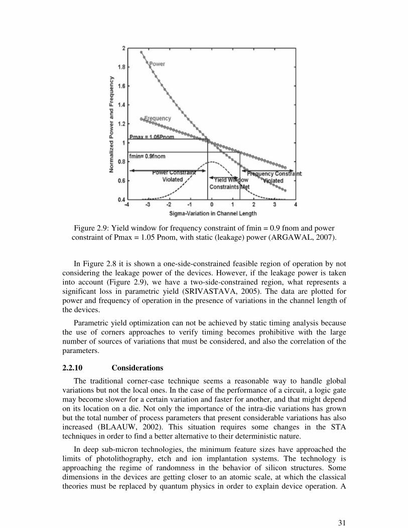
Figure 2.8: Yield window for frequency constraint of fmin = 0.9 fnom and powerconstraint of Pmax = 1.05 Pnom, for negligible static (leakage) power (ARGAWAL,
2007).
31
Figure 2.9: Yield window for frequency constraint of fmin = 0.9 fnom and powerconstraint of Pmax = 1.05 Pnom, with static (leakage) power (ARGAWAL, 2007).
In Figure 2.8 it is shown a one-side-constrained feasible region of operation by notconsidering the leakage power of the devices. However, if the leakage power is takeninto account (Figure 2.9), we have a two-side-constrained region, what represents asignificant loss in parametric yield (SRIVASTAVA, 2005). The data are plotted forpower and frequency of operation in the presence of variations in the channel length ofthe devices.
Parametric yield optimization can not be achieved by static timing analysis becausethe use of corners approaches to verify timing becomes prohibitive with the largenumber of sources of variations that must be considered, and also the correlation of theparameters.
2.2.10 Considerations
The traditional corner-case technique seems a reasonable way to handle globalvariations but not the local ones. In the case of the performance of a circuit, a logic gatemay become slower for a certain variation and faster for another, and that might dependon its location on a die. Not only the importance of the intra-die variations has grownbut the total number of process parameters that present considerable variations has alsoincreased (BLAAUW, 2002). This situation requires some changes in the STAtechniques in order to find a better alternative to their deterministic nature.
In deep sub-micron technologies, the minimum feature sizes have approached thelimits of photolithography, etch and ion implantation systems. The technology isapproaching the regime of randomness in the behavior of silicon structures. Somedimensions in the devices are getting closer to an atomic scale, at which the classicaltheories must be replaced by quantum physics in order to explain device operation. A

32
32
large variability in performance and power consumption among different chips isexpected since the device parameters, such as channel length, oxide thickness, thresholdvoltage and random placement of dopants in channel, may have variations. Since theprocess variations become a more significant problem because of the aggressivetechnology scaling, a shift from deterministic to statistical analysis for circuit designsmay reduce the conservatism and risk that is present while applying the traditionaltechnique.
The variation in a physical parameter can cause more than one electrical parametersto vary, giving rise to a correlation of these electrical parameters. Correlation ofparameters variations must be considered in timing and power analysis, otherwisepessimistic results may result. As an example, gate width variations in a transistor havedifferent (inversely correlated) impacts on the resistance (R) and capacitance (C) of thedevice. It means that while a variation in gate width decreases the resistance, itincreases the capacitance, and worst-case values for R and C would lead to unrealisticRC estimates. The number of random variables one deal with increases rapidly whenintra-die variations are considered, and that increases computational cost.
Statistical analysis overcomes the difficulties of the traditional methodology bytreating the characteristics of the circuits, such as signal delay and power consumption,as probability density functions (PDF). The process parameters are no longer fixedvalues but random variables with certain statistical distributions. A statistical approachmust be developed in order to predict performance and power consumption moreaccurately, making it possible not only to analyze the circuit efficiently, but also tooptimize it.
2.3 Analysis of the Impact of Parameter Variation on the ThresholdVoltage Variation
This section is intended to validate the use of non-correlated variations for thethreshold voltages (VTH) of MOS transistors, by considering that each transistor has arandom VTH variation, independently on its position on the die. The impact of channellength (L) and oxide thickness (Tox) variations on VTH were compared to the effectcaused on the same electrical parameter by random-dopant fluctuations (RDF). RDFcause different and non-correlated variations in VTH of transistors whether they areplaced in the vicinity of each other or not. The opposite happens to variations in L andTox that presents strong correlations across the die area.
2.3.1 Variations due to Random-Dopant Fluctuations, Channel Lengthand Oxide Thickness Variations
Nanoscaled MOS transistors present statistical variation in their threshold voltagesbecause of random number and placement of dopants in the channel region. Thefollowing equation is used to incorportate this effect in the threshold voltage deviation(HOON, 2004):
Vth
q
Cox
Na Wdm
3 L W (2.2)

33
where L and W are the channel length and width of the transistor, respectively. Na is thesubstrate doping concentration, q is the electron charge, Cox is the oxide capacitance andWdm is the maximum depletion layer width and it is given by the equation (ROY, 2003):
Wdm
4 si K T lnN
a
ni
q2 Na (2.3)
where ni is the intrinsic carrier concentration, K is the Boltzmann constant, T is thetemperature and εsi is the dielectric permissivity of Si.
In order to calculate the dependence of threshold voltage on the channel length ofshort-channel transistors, it is used an equation that quantifies the drain-induced barrierlowering (DIBL) effect (XUEMEI, 2003):
V th DIBL th Leff 2 V bi s Vds (2.4)
where Vbi is the built-in voltage of the source/drain junctions and is given by equation(2.5). Φs is the surface potential and is calculated through equation (2.6).
Vbi
K T
qln
NDEP NSD
ni2
(2.5)
s
2 K T
qln
Nch
ni (2.6)
θth is the short-channel effect coefficient (XUEMEI, 2003) and has a strongdependence on the channel length approached by equation (2.7):
th Leff expLeff
2 lt2 exp
Lefflt (2.7)
lt stands for the characteristic length and is calculated by using equation (2.8).
ltsi tox Xdep
ox (2.8)
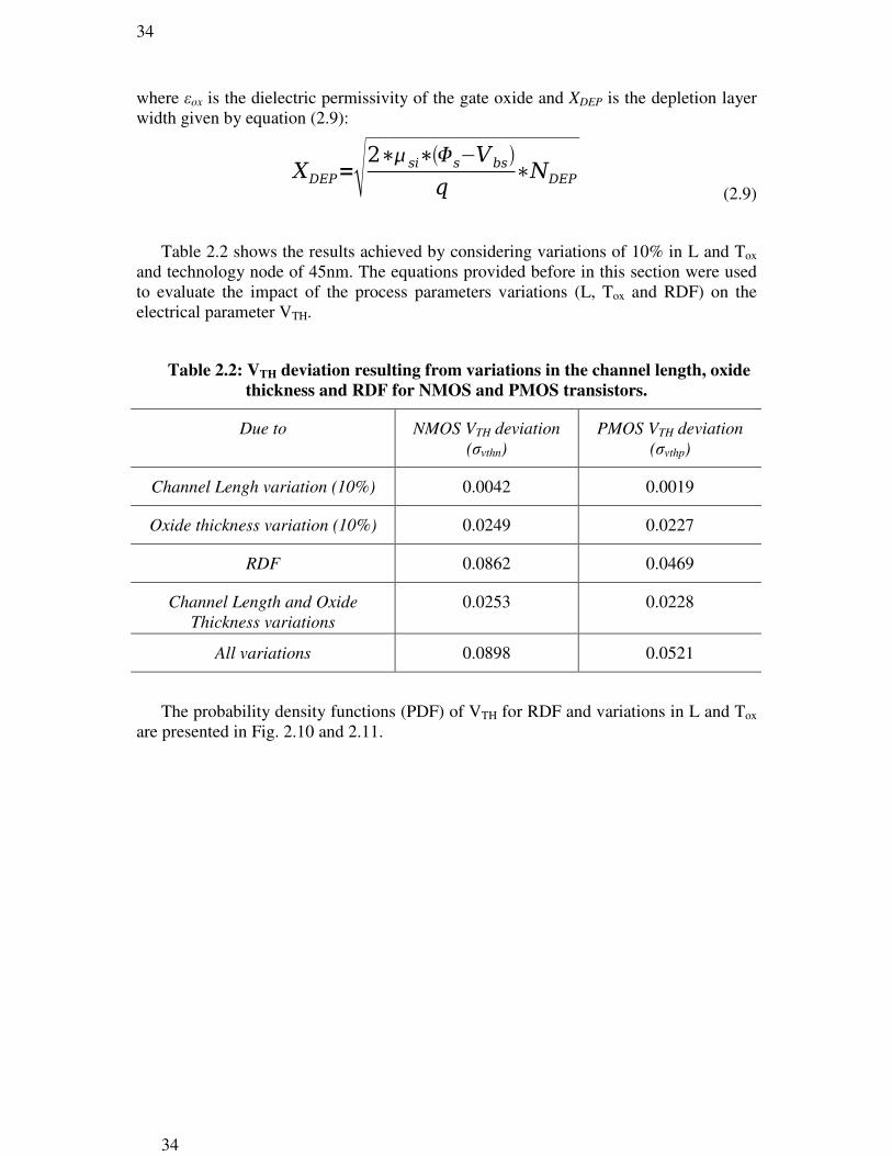
34
34
where εox is the dielectric permissivity of the gate oxide and XDEP is the depletion layerwidth given by equation (2.9):
XDEP
2 si s Vbs
qNDEP
(2.9)
Table 2.2 shows the results achieved by considering variations of 10% in L and Tox
and technology node of 45nm. The equations provided before in this section were usedto evaluate the impact of the process parameters variations (L, Tox and RDF) on theelectrical parameter VTH.
Table 2.2: VTH deviation resulting from variations in the channel length, oxidethickness and RDF for NMOS and PMOS transistors.
Due to NMOS VTH deviation
(σvthn)
PMOS VTH deviation
(σvthp)
Channel Lengh variation (10%) 0.0042 0.0019
Oxide thickness variation (10%) 0.0249 0.0227
RDF 0.0862 0.0469
Channel Length and Oxide
Thickness variations
0.0253 0.0228
All variations 0.0898 0.0521
The probability density functions (PDF) of VTH for RDF and variations in L and Tox
are presented in Fig. 2.10 and 2.11.

35
0,0 0,1 0,2 0,3 0,4 0,5 0,6 0,7 0,8 0,9 1,0 1,1 1,2
0,0
0,2
0,4
0,6
0,8
1,0
1,2
Norm
aliz
ed T
hre
shold
Voltage D
istr
ibu
tion
NMOS Threshold Voltage
∆Toxn
∆Toxn
, ∆Leffn
, RDF
∆Toxn
and ∆Leffn
RDF ∆L
effn
Figure 2.10: Threshold voltage PDFs of NMOS for process parameter variations.
It is observed that variations of L cause little deviation in VTH distribution. Astronger deviation is resulted from variations in Tox, but RDF present the mostimportant influence on VTH PDF. In this sense, it is quite acceptable the approachconsidered in this work, which makes use of non-correlated VTH variations.
0,1 0,2 0,3 0,4 0,5 0,6 0,7 0,8 0,9
0,0
0,2
0,4
0,6
0,8
1,0
1,2
No
rmaliz
ed T
hre
sh
old
Vo
lta
ge D
istr
ibu
tion
PMOS Threshold Voltage
∆Toxp
∆Toxp
and ∆Leffp
, RDF
∆Toxp
and ∆Leffp
RDF ∆L
effp
Figure 2.11. Threshold voltage PDFs of PMOS for process parameter variations.
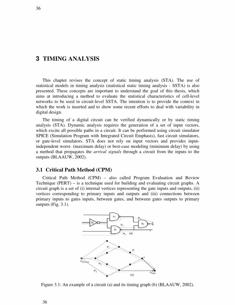
36
36
3 TIMING ANALYSIS
This chapter revises the concept of static timing analysis (STA). The use ofstatistical models in timing analysis (statistical static timing analysis - SSTA) is alsopresented. These concepts are important to understand the goal of this thesis, whichaims at introducing a method to evaluate the statistical characteristics of cell-levelnetworks to be used in circuit-level SSTA. The intention is to provide the context inwhich the work is inserted and to show some recent efforts to deal with variability indigital design.
The timing of a digital circuit can be verified dynamically or by static timinganalysis (STA). Dynamic analysis requires the generation of a set of input vectors,which excite all possible paths in a circuit. It can be performed using circuit simulatorSPICE (Simulation Program with Integrated Circuit Emphasis), fast circuit simulators,or gate-level simulators. STA does not rely on input vectors and provides input-independent worst- (maximum delay) or best-case modeling (minimum delay) by usinga method that propagates the arrival signals through a circuit from the inputs to theoutputs (BLAAUW, 2002).
3.1 Critical Path Method (CPM)Critical Path Method (CPM) – also called Program Evaluation and Review
Technique (PERT) – is a technique used for building and evaluating circuit graphs. Acircuit graph is a set of (i) internal vertices representing the gate inputs and outputs, (ii)vertices corresponding to primary inputs and outputs and (iii) connections betweenprimary inputs to gates inputs, between gates, and between gates outputs to primaryoutputs (Fig. 3.1).
Figure 3.1: An example of a circuit (a) and its timing graph (b) (BLAAUW, 2002).

37
The procedure consists in propagating the delay of gates and interconnects of acircuit from the source node to the sink node using sum or max operation in order tofind the critical path. The critical path is the one between an input and an output withthe maximum delay. The individual gates are pre-characterized and their timingspecifications are used to calculate the arrival time at each node. As the arrival timestraverse gates, the delay of the gate is added to the arrival time and a maximum value isselected in the case of a multi-fanin node.
Since static timing analysis must provide correctness for any input vector, accurategate and interconnect timing modeling is demanded. In a standard-cell flow, the gatedelay is typically pre-characterized for different capacitive loads and input transitiontimes. The libraries contain analytical expressions for the delay or timing tables that aregenerated by performing circuit simulation with SPICE after the extraction of the layoutparasitics for cells in the library. STA assumes full correlation of process parameterswithin a die, what means that all devices and interconnect on a chip slow down or speedup in tandem. That would be a reasonable approach if no variations within the same dietook place (CHIANG, 2007).
Traditional deterministic computer-aided-design (CAD) tools rely on the use ofcorner-case models that set worst-case, best-case or nominal values for the processparameters of an integrated circuit while analyzing its performance and powerconsumption (SRIVASTAVA, 2005). For each process condition the delay of the gatesat that process condition is specified. This methodology implies in a great number ofsimulation runs if the effects of a large amount of sources of variations are to beconsidered, and can end up being pessimistic (worst-case assumptions) or optimistic(best-case assumptions), and risky at the same time, since not every corner is simulated(VISWESWARIAH, 2006). A deterministic description does not present the variance ofa process parameter, but only its mean value. Worst-case values are taken at theanalyzed corners, what is a pessimistic assumption, but since it is intractable to cover allpossible corners, the missing ones may lead to failures that are not detected beforemanufacturing the chip. Another drawback of a corner-based STA is the possibility ofidentifying incorrect critical paths. These paths are obtained by assuming all the deviceswith the same deviations characteristics, but delay variations can lead to change ofcritical paths (PAN, 2005).
3.2 Statistical ConceptsThe value of a parameter cannot be predicted exactly. This happens because the
behavior is (a) unknown, (b) truly random or (c) because it cannot be represented by amodel (ORSHANSKY, 2008). As already said before, in a statistical fashion the processparameters are defined as random variables.
A random variable (RV) is any function that assigns a numerical value to eachpossible outcome of some experiment (ORSHANSKY, 2008). A finite number ofoutcomes is represented by a discrete RV and an infinite number of outcomes isrepresented by a continuous RV. A common case of discrete random variables that areencountered in circuits manufacturing is where the RV, let's call it X, can have one oftwo values. One example is the probability that a circuit has of failing or workingcorrectly. If we get a sample of circuits with the same failure probability to be tested,then the number of working circuits is a Binomial random variable.

38
38
Normal, uniform, and log-normal random variables are some of the continuous RVencountered in statistical design applications. Various physical phenomena andparameters follow normal distribution. A normal random variable is described by aprobability density function:
f x1
2e
1
2.x
2
(3.1)
where µ is the mean and σ is the standard deviation. For a continuous random variable,the probability density function is represented by a curve such that the area under thecurve between two numbers is the probability that the random variable will be found inthe interval limited by those two numbers (Figure 3.2).
Figure 3.2: Normal distribution of a random variable. The horizontal axis represent thestandard deviation (MODE, 1966).
A cumulative distribution function (CDF), which is the integral of the PDF is alsoused to represent an RV:
P X a F aa
1
2e
1
2.x
2
. dx (3.2)
and identifies the probability that the random variable X takes on a value less than orequal to a.
A random variable is fully characterized by its PDF and CDF, and partiallydescribed in terms of the moments of its probability distribution. The most importantmoments of a RV are the first moment, the mean (µ), and the second moment that is the
variance (σ2). Usually, the random variables in a statistical analysis of a circuit presentsome kind of correlation in their behavior. This codependence can be evaluated byusing a covariance matrix that defines pair-wise correlations between variables. Thecovariance measures how much two RV vary together.
A linear combination of normal random variables also follows a normal distribution,but if the function is not linear in the RV, its distribution is not normal. However, anapproximate method based on a first-order Taylor-series expansion of the function canbe used if it is nearly linear in the small range.

39
3.3 Statistical Static Timing Analysis (SSTA)Since cell-level statistical timing analysis was performed in this work, it is important
to be aware of the great potential it comes up with for circuit analysis and optimization.Some statisical approaches and techniques are then presented here.
The extensive research in timing analysis shows the need for a new method ofdealing with the following issues (ARGAWAL, 2003): (i) the ability to control criticaldevice parameters is becoming restricted, since the process geometries continue toshrink, what results in significant variations of these parameters; (ii) the total number ofprocess parameters that exhibit variations has increased, making the number of corner
files (files that specify the characteristics of the gate for each process condition)increases rapidly; (iii) within-die (intra-die) variations have become a significantcomponent of the total variation; (iv) in addition to device parameters interconnectparameters must be considered.
The deterministic formulation of static timing analysis treats the delay of gates andpaths as fixed numbers, thus reducing a probabilistic problem to an arithmetical one.Statistical timing analysis may manipulate explicit parametric functions of delay onprocess parameters naturally, thus removing the need to identify the worst-caseconditions a priori. In SSTA the performance metrics of gates and wires are modeled bystochastic values.
It is important to analyze circuit performance under process variation for yieldprediction as well as for circuit optimization. The deterministic-based optimization forthe circuit delay tends to concern only about the critical and near critical paths delaysince there is no incentive to improve path delays that are not critical. In statisticalanalysis there is no sense in trying to identify a single path of the circuit as being thecritical path, or the path with the maximum delay. Critical paths are then defined as aset of paths with high probability of becoming the slowest path in the circuit(SRIVASTAVA, 2005).
3.4 Statistical Solution Approaches
3.4.1 Numerical Integration Method
This kind of method operates in the space of manufacturing variations (parameterspace) or in the space of path delays (performance space) (JESS, 2006). Performance-space methods manipulate timing variables such as arrival times and slacks as statisticalquantities. The joint probability density function (JPDF) of the delays of all paths isintegrated over a cube of side equal to the required delay and of dimensionality equal tothe number of paths. Parameter-space methods perform manipulations in the space ofthe sources of variation. The JPDF of the sources of parametric variation are integratedover a complex feasible region in relatively low-dimensional space.
3.4.2 Monte Carlo Method
Monte Carlo simulation is a method for iteratively evaluating a deterministic modelusing sets of random variables as inputs. This method can sample a system in a numberof random configurations and that data can be used to describe the system as a whole.By performing a full-scale transistor-level Monte-Carlo simulation of a circuit, one getsthe most accurate way of incorporating the process variation effects into timing

40
40
analysis. It generates samples points for a given delay distribution and runs a statictiming analyzer at each point. The results are put together to form the delay distribution(SAPATNEKAR, 2004).
3.4.3 Probabilistic Analysis Methods
Probabilistic methods usually propagate arrival-times through the timing graph byperforming statistical sum and maximum operations. In these approaches the gatedelays and arrival times are computed as random variables whose probability densityfunctions (PDFs) are propagated through the circuit, and hence, the addition andmaximum operations becomes a convolution operation and a statistical maximum,respectively. It means that once the delay of gates and interconnects in a circuit ismodeled as a Gaussian random variable, the delay of a path is a Gaussian randomvariable as well (Figure 3.3).
Figure 3.3: Gate and interconnect delays represented as probability density functions(SRIVASTAVA, 2005).
In SSTA the maximum of two random variables is not uniquely defined and acriterion must be used in order to compute the maximum of the variables.
3.5 Delay Modeling
3.5.1 Introduction
A digital circuit is constituted by transistors, usually organized into gates that driveinterconnect wires. Typical approaches to timing analysis divide the design into stages,with each stage consisting of a gate output and the interconnect path it drives. Digitalsystems are often designed at the gate or cell level, making it possible to pre-characterize the gate and cell delay for timing analysis (CELIK, 2002). The cell delaysand transitions are generally expressed empirically as a function of load capacitance andinput signal transition. A delay calculator expects a certain waveform at the fanout as afunction of the waveform at the switching input pin.
At this moment, that would be appropriate to focus on two parameters of awaveform, that are very important for timing analysis: delay and transition time.

41
3.5.1.1 Delay
Delay is defined as the interval between the time when the input waveform crosses aspecified threshold, and when the output waveform crosses a given threshold. Thesetwo points are usually set as the points at which the waveforms reach half of their finalvalue (50% point) while in transition (Figure 3.4).
Figure 3.4: The 50% delay and transition time of a waveform.
3.5.1.2 Transition Time
The transition time of a waveform says how long it takes to reach its final value in atransition. Since most such transitions involve exponentials, it is commonly used theinterval between the points 10-90% or 20-80% to measure the transition time.
3.5.2 Gate and Interconnect Timing Models
The components in a circuit can be represented by a model, which is an abstractionof the component behavior. By conceiving a model for each component, one can dealwith its physical aspects in a more tractable way. A trade-off between accuracy andcomplexity must be taken into account in order to decide whether a model is reasonableor not. In contrast to designing circuits at the transistor level, gate or cell level designcan reduce the design effort by pre-characterizing the gates and cells for timinganalysis.
Delay evaluation in the Very Large Scale Integration (VLSI) design is a greatconcern and it becomes more critical in nowadays deep sub-micron technology. It isnecessary to adequately account for nanometer effects during timing analysis, in orderto predict the performance of the circuit accurately. Static Timing Analysis is a feasiblemethod for chip-level analysis of the time constants of a circuit without simulation.Depending on the models used for gates and interconnects its accuracy might satisfy thetiming constraints of integration-scaled circuits (KUONO, 2005).
The interconnect lengths do not scale in proportion to shrinking chip area, and thatresults in the dominance of the delay due to interconnect over the delay contributed bythe gate. The great shrinking in size presented in recent technologies leads to some
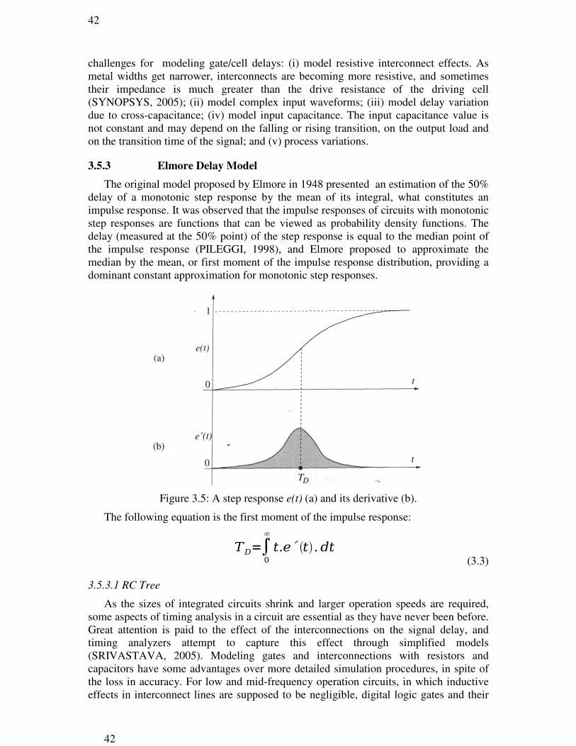
42
42
challenges for modeling gate/cell delays: (i) model resistive interconnect effects. Asmetal widths get narrower, interconnects are becoming more resistive, and sometimestheir impedance is much greater than the drive resistance of the driving cell(SYNOPSYS, 2005); (ii) model complex input waveforms; (iii) model delay variationdue to cross-capacitance; (iv) model input capacitance. The input capacitance value isnot constant and may depend on the falling or rising transition, on the output load andon the transition time of the signal; and (v) process variations.
3.5.3 Elmore Delay Model
The original model proposed by Elmore in 1948 presented an estimation of the 50%delay of a monotonic step response by the mean of its integral, what constitutes animpulse response. It was observed that the impulse responses of circuits with monotonicstep responses are functions that can be viewed as probability density functions. Thedelay (measured at the 50% point) of the step response is equal to the median point ofthe impulse response (PILEGGI, 1998), and Elmore proposed to approximate themedian by the mean, or first moment of the impulse response distribution, providing adominant constant approximation for monotonic step responses.
Figure 3.5: A step response e(t) (a) and its derivative (b).
The following equation is the first moment of the impulse response:
TD0
t.e´ t .dt (3.3)
3.5.3.1 RC Tree
As the sizes of integrated circuits shrink and larger operation speeds are required,some aspects of timing analysis in a circuit are essential as they have never been before.Great attention is paid to the effect of the interconnections on the signal delay, andtiming analyzers attempt to capture this effect through simplified models(SRIVASTAVA, 2005). Modeling gates and interconnections with resistors andcapacitors have some advantages over more detailed simulation procedures, in spite ofthe loss in accuracy. For low and mid-frequency operation circuits, in which inductiveeffects in interconnect lines are supposed to be negligible, digital logic gates and their
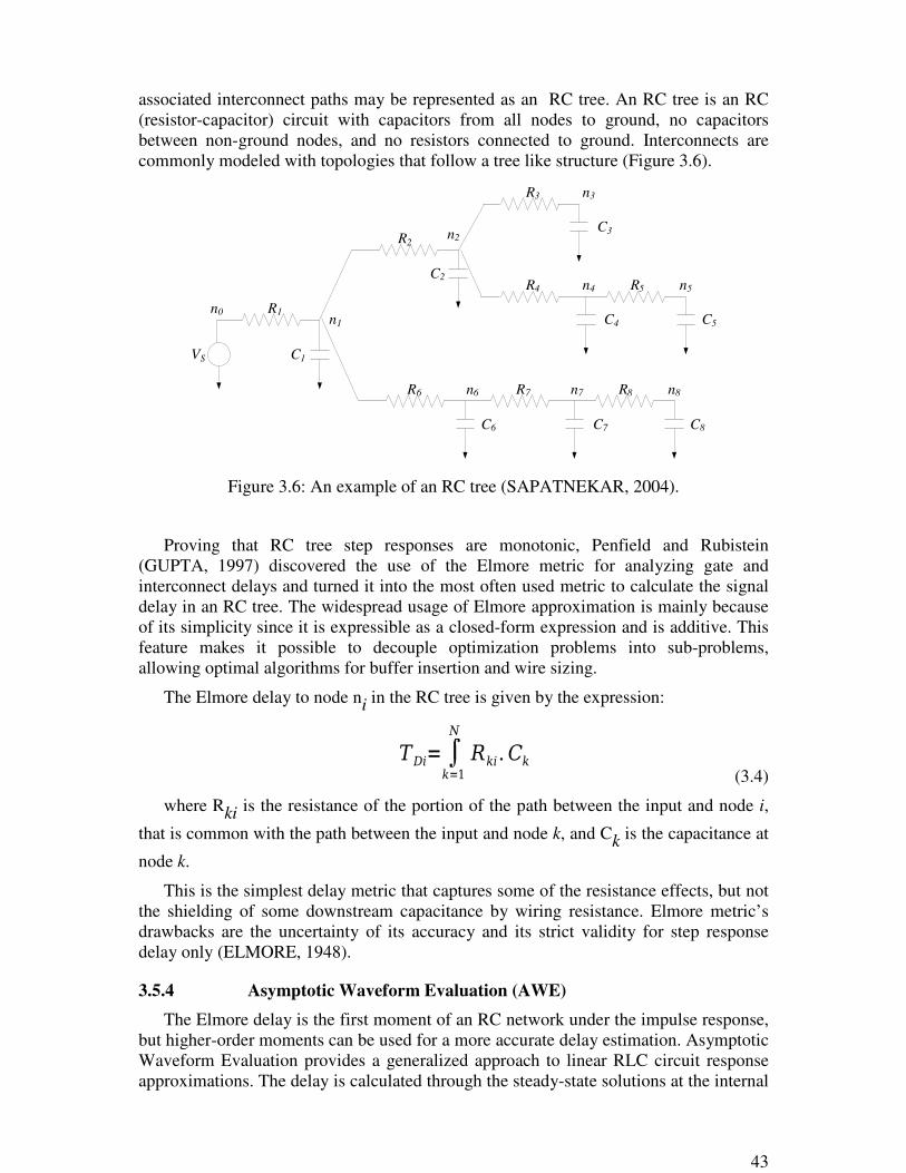
43
associated interconnect paths may be represented as an RC tree. An RC tree is an RC(resistor-capacitor) circuit with capacitors from all nodes to ground, no capacitorsbetween non-ground nodes, and no resistors connected to ground. Interconnects arecommonly modeled with topologies that follow a tree like structure (Figure 3.6).
VS
R1
R2
R3
R4 R5
R6 R7 R8
n0n1
n2
n3
n4 n5
n6 n7 n8
C1
C2
C3
C4 C5
C6 C7 C8
Figure 3.6: An example of an RC tree (SAPATNEKAR, 2004).
Proving that RC tree step responses are monotonic, Penfield and Rubistein(GUPTA, 1997) discovered the use of the Elmore metric for analyzing gate andinterconnect delays and turned it into the most often used metric to calculate the signaldelay in an RC tree. The widespread usage of Elmore approximation is mainly becauseof its simplicity since it is expressible as a closed-form expression and is additive. Thisfeature makes it possible to decouple optimization problems into sub-problems,allowing optimal algorithms for buffer insertion and wire sizing.
The Elmore delay to node ni in the RC tree is given by the expression:
TDik 1
N
Rki.Ck
(3.4)
where Rki is the resistance of the portion of the path between the input and node i,
that is common with the path between the input and node k, and Ck is the capacitance at
node k.
This is the simplest delay metric that captures some of the resistance effects, but notthe shielding of some downstream capacitance by wiring resistance. Elmore metric’sdrawbacks are the uncertainty of its accuracy and its strict validity for step responsedelay only (ELMORE, 1948).
3.5.4 Asymptotic Waveform Evaluation (AWE)
The Elmore delay is the first moment of an RC network under the impulse response,but higher-order moments can be used for a more accurate delay estimation. AsymptoticWaveform Evaluation provides a generalized approach to linear RLC circuit responseapproximations. The delay is calculated through the steady-state solutions at the internal

44
44
nodes of the network (SAPATNEKAR, 2004). A set of independent state variables mustbe chosen for a complete characterization of the RC network (as considered in thiswork) by means of the state equations.
The RC network can be described in terms of the following state equations:
x' A.x B.uy C.x D.u (3.5)
where x denote the state vector, which in our case is simply the vector of thecapacitance voltages. The input vector u is the vector of the input independent voltageand current sources, and the output vector y is the vector of the output node voltages.The matrices A, B, C and D can be obtained in terms of the resistor and capacitor valuesand are dependent on the topology of the network. Figure 3.7 shows an RC network asan example.
Figure 3.7: RC system.
The matrices G (conductance matrix) and C (capacitance matrix) are taken from thecircuit equations:
Calculating the values of the variables:
G X C X ' E (3.6)
where X is the variables vector
The first moment is calculating by applying a DC voltage to the circuit (capacitorsare open):
G m 0 E0 (3.7)

45
For Eo = 1,
m0 = [1 1 1 1 1 1 0]'
The higher moments are calculated by taking away external sources:
G mi
C mi 1 (3.8)
The calculated moments are matched via Padé approximation to reduced-orderfunction models, which are used to characterize the circuit time and frequency domainresponses with high accuracy.
A normalized transfer function for a linear system can be expressed as:
H s1 a1. s a2. s
2... an. s
n
1 b1. s b2. s2... bm. s
m
(3.9)
where m>n. The transfer function H(s) can be expanded into a power series with respectto s:
H s m0 m1 . s m2 . s2... (3.10)
where mi are the moments.
A Padé approximant is a lower order transfer function and it is characterized by itsorder (SAPATNEKAR, 2004). AWE constructs a q-pole transfer function H’(s) toapproximate the actual transfer function H(s):
H' si 1
q kis pi (3.11)
where pi and ki are the determined poles and residues. The corresponding time domainimpulse response is:
h' ti 1
q
ki .epi.t
(3.12)
In AWE the delay of any output node i in a general RC network is defined as thetime taken by the asymptotic approximation of the voltage at the node to reach itssteady-state value. For the case of an RC tree model, a first-order AWE approximationreduces to the RC tree methods.
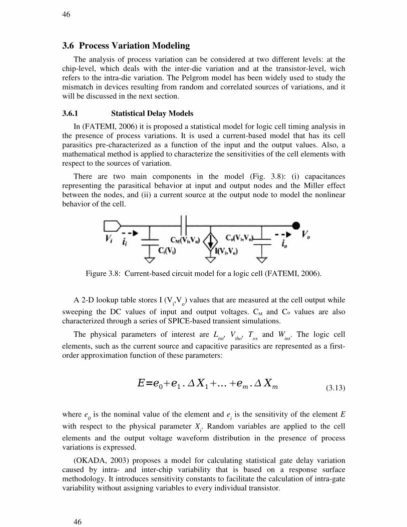
46
46
3.6 Process Variation ModelingThe analysis of process variation can be considered at two different levels: at the
chip-level, which deals with the inter-die variation and at the transistor-level, wichrefers to the intra-die variation. The Pelgrom model has been widely used to study themismatch in devices resulting from random and correlated sources of variations, and itwill be discussed in the next section.
3.6.1 Statistical Delay Models
In (FATEMI, 2006) it is proposed a statistical model for logic cell timing analysis inthe presence of process variations. It is used a current-based model that has its cellparasitics pre-characterized as a function of the input and the output values. Also, amathematical method is applied to characterize the sensitivities of the cell elements withrespect to the sources of variation.
There are two main components in the model (Fig. 3.8): (i) capacitancesrepresenting the parasitical behavior at input and output nodes and the Miller effectbetween the nodes, and (ii) a current source at the output node to model the nonlinearbehavior of the cell.
Figure 3.8: Current-based circuit model for a logic cell (FATEMI, 2006).
A 2-D lookup table stores I (Vi,V
o) values that are measured at the cell output while
sweeping the DC values of input and output voltages. CM and Co values are alsocharacterized through a series of SPICE-based transient simulations.
The physical parameters of interest are Lint
, Vtho
, Tox
and Wint
. The logic cell
elements, such as the current source and capacitive parasitics are represented as a first-order approximation function of these parameters:
E e0 e1 . X1 ... em . Xm (3.13)
where e0 is the nominal value of the element and e
i is the sensitivity of the element E
with respect to the physical parameter Xi. Random variables are applied to the cell
elements and the output voltage waveform distribution in the presence of processvariations is expressed.
(OKADA, 2003) proposes a model for calculating statistical gate delay variationcaused by intra- and inter-chip variability that is based on a response surfacemethodology. It introduces sensitivity constants to facilitate the calculation of intra-gatevariability without assigning variables to every individual transistor.
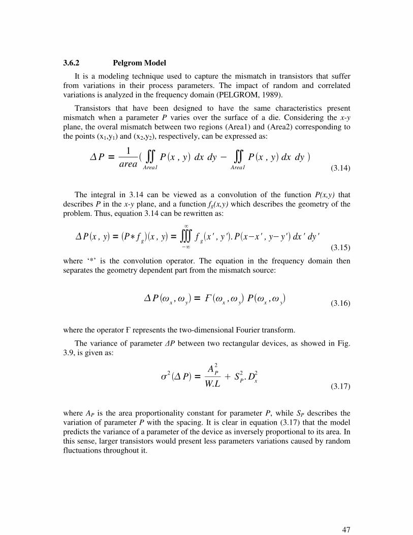
47
3.6.2 Pelgrom Model
It is a modeling technique used to capture the mismatch in transistors that sufferfrom variations in their process parameters. The impact of random and correlatedvariations is analyzed in the frequency domain (PELGROM, 1989).
Transistors that have been designed to have the same characteristics presentmismatch when a parameter P varies over the surface of a die. Considering the x-y
plane, the overal mismatch between two regions (Area1) and (Area2) corresponding tothe points (x1,y1) and (x2,y2), respectively, can be expressed as:
P1
area Area1
P x , y dx dyArea1
P x , y dx dy (3.14)
The integral in 3.14 can be viewed as a convolution of the function P(x,y) thatdescribes P in the x-y plane, and a function fg(x,y) which describes the geometry of theproblem. Thus, equation 3.14 can be rewritten as:
P x , y P fg
x , y fg
x ' , y ' . P x x ' , y y' dx ' dy ' (3.15)
where ‘*’ is the convolution operator. The equation in the frequency domain thenseparates the geometry dependent part from the mismatch source:
P ωx,ω
yω
x,ω
yP ω
x,ω
y (3.16)
where the operator Ғ represents the two-dimensional Fourier transform.
The variance of parameter ∆P between two rectangular devices, as showed in Fig.3.9, is given as:
2P
AP
2
W.LS
P
2 . Dx
2
(3.17)
where AP is the area proportionality constant for parameter P, while SP describes thevariation of parameter P with the spacing. It is clear in equation (3.17) that the modelpredicts the variance of a parameter of the device as inversely proportional to its area. Inthis sense, larger transistors would present less parameters variations caused by randomfluctuations throughout it.

48
48
Figure 3.9: Representation of transistors that lie on the x-axis separated by a distance x.

49
4 PROPOSAL AND METHODOLOGY
4.1 IntroductionAs already explained in CHAPTER 2, performance and power consumption of an
integrated circuit is impacted by the fabrication process variations (channel length andwidth, gate oxide thickness, doping concentration and distribution etc). Regarding MOSfabrication process, variation effects do not scale proportionally with the designdimensions, causing the relative impact of the critical dimension variations to increasewith each new technology. In nanoscale CMOS devices, the reduced average number ofdopant atoms in the channel of a transistor causes the effect of random dopantfluctuations on its threshold voltage to increase (MAHMOODI, 2005).
Physical parameters are susceptible to random variations and the statistical nature ofprocess characteristics makes it possible to consider the process parameters and theirvariations as random variables represented by their probability distribution function(PDF). In (MAHMOODI, 2005) the delay distributions of some logic gates areestimated by considering threshold voltage variations due to random-dopantfluctuations. Regarding the threshold voltage, its standard deviation is modeled asdepending on the transistors dimensions (channel length and width, gate oxide thicknessetc) and doping concentration.
The general goals of the present work are the analysis and variability estimation oftransistors arrangements in order to point at the networks whose performance is as lesssusceptible as possible to the parameters variations of devices. The first part of the studyis based on statistical (Monte Carlo) simulations, and it is intended to shed a light on thebehavior of performance variability of the basic transistors structures and logic gates.The second and main focus of this work is on the implementation of a semi-empiricalestimation method that describes and predicts this variability according to differenttransistors arrangements.
Besides the motivation and proposal of the work, this chapter describes in details themethodology applied in the analysis in order to figure out how variability in thethreshold voltage of transistors affects a CMOS gate performance in different transistorsnetwork arrangements and switching situations. These data are able to indicatetopologies that are more affected by variations and how each transistor resistance isaffected by changes in the threshold voltages of transistors in the network.
4.2 MotivationParametric yield improvement may be achieved by reducing the variability of
performance and power consumption of a cell. Figure 2.9 showed a two-side-

50
50
constrained region of operation of devices that suffer variations in their channel length.A high sensitivity of a device to variations in its parameters means that the yieldwindow, limited by frequency and power constraints, is narrower than when a device ismore immune to variability. A narrow yield window implies in a high quantity ofmanufactured chips that may not satisfy operational specification, leading to a highercost of fabrication, since many chips may become useless.
In general, the behavior of signal propagation delays in transistors networks arewell-know when it concerns to the increase or decrease of the number of devices in astack or in a parallel array. Also, one can say that a change in the logic gate delaycaused by a change in the position of the switching transistor in the array is at leastqualitatively predictable. In many cases, the use of complex gates instead of smallerlogic gates can lead to a faster signal propagation (SAKURAI, 1991). However,variability characteristics of the cells are becoming more and more important, since theycan affect drastically the performance of the circuit and consequently the parametricyield. Some guidelines applied before in order to guarantee the functionality of a designin especific conditions must be reviewed for the sake of the yield. It is not only aquestion of reducing the delay of the cell anymore, but also providing a way that itsvariation do not compromises the operation of the cell.
Detailed electrical simulations of circuits are able to provide precise results for theirperformance, but they are computationally expensive. Timing models are necessary intiming analysis in order to perform a fast evaluation of the circuit. The models used inthe analysis must represent the true behavior of the cell under certain conditions. Theauthors in (WEBEL, 2004) present a semi-empirical model based on type, geometry ofthe gates, body effect of transistors, slope of input signals, capacitance loads andthreshold logic voltage. It adds a new timing parameter (latency time) which is added tothe usual RC time constant.
Static timing analysis is usually used to find the critical points of the circuit thataffect the critical path delay. Conventional sizing tools size the gates to optimize areaand power consumption while meeting the desired delay constraint (SAPATNEKAR,1993). The transistor widths are then sized to meet the desired delay constraint whilekeeping the power consumption and area within a limit. However, due to randomprocess parameter variation, a large number of chips may not meet the required delay.
The traditional design efforts guided only by the best, worst and the nominal casemodels for the device parameters over- or underestimate the impact of variation.Approaches in the area of statistical static timing analysis have appeared to overcomethe issues of corner-based methodology. The authors in (CAO, 2005) developes aphysical model for analysis and prediction of circuit performance variability bycoupling the Alpha-Power law based model with considerations of short-channeleffects such as velocity saturation and threshold voltage dependence on channel lengthand drain bias (DIBL).
(CHOI, 2004) proposes a statistical design technique considering both inter- andintra-die variation of process parameters. The effects of process variations on the gatedelay is pre-characterized and acessed on the fly during statistical timing analysis. Thegoal is to resize the transistor widths with minimal increase in area and powerconsumption while improving the confidence that the circuit meets the delay constraintunder process variations. They have developed a sizing tool based on LagragianRelaxation (LR) algorithm for global optimization of transistor widths.

51
Aiming at improving the parametric yield of chips, more robust cells could beachieved by choosing the adequate logic style and network arrangement for a certainlogic function. One way of using the information of which cells are more immune tovariability in a circuit design is to attribute a “cost” for each cell in a cell library relatedto its sensitivity to variations. This cost could be used in technology mapping to guidethe use of less sensitive cells in a circuit that demands more robustness to variability.(SINGH, 2005) describes a new technology mapping algorithm that performs librarybinding to maximize parametric yield limited both by timing and power constraints. Itproposes a statistical technology mapping that find a circuit mapping such that the yieldat a required power objective is maximized while meeting the required timingconstraints at a pre-specified yield level. It is indicated that a statistical technologymapping algorithm can produce mappings with reduced power consumption at the samepower and timing yield levels.
4.3 ProposalThe goal of this work is to provide means to parametric yield improvement of ICs
through a variability-aware design. The generation of cells that are more robust inrelation to variability and the improvement of the parametric yield of a given circuitrequires the knowledgement of how the parameters variations impact the performanceof the cell. Statistical simulations (Monte Carlo) are able to provide reliable results oncethe parameters have random variations that follow a Gaussian probability densityfunction (SRIVASTAVA, 2005), but are computationally costly. That is the reason whybesides analyzing some transistors networks through simulations, a semi-empiricalmethod that predicts performance variability according to the transistors arrangementsis developed and proposed.
4.4 MethodologyThe characterization is achieved through statistical (Monte Carlo) simulations of the
networks. The analysis starts with simple configurations and later with more complexones. The results provided by the simulations are then analyzed in order to providesome guidelines that can be used for designing more robust transistors networks. Afterthese primary observations, simulations of some well-known logic cells are performedin order to verify the credibility of those guidelines first provided.
As a first insight, some topologies are analyzed with statistical (Monte Carlo)simulations to estimate the timing variability and compare these results with thoseachieved by using the semi-empirical method to be proposed. Different numbers of N-or PMOS transistors were considered in a stacking, in a parallel arrangement or in amixed (series-parallel) network, and also, different positions for the switching device inrelation to the output node. The results achieved with some simple transistorarrangements are intended to be the starting point to analyze and predict the variabilityof logic gates usually present in cells library to be used in technology mapping. In thissense, an important step is to analyze the VTH variations impact on largely used logic
gates presenting different topologies and different transistors networks arrangements.
Electrical simulations are proceeded in order to show the variability performance ofinverter, NAND and NOR, XOR (in different configurations) and AOI (AND-OR-INVERTER) gates. Also, different topologies of full adders are analyzed. The

52
52
simulations are able to provide important information on the behavior of the cellsaccording to their topology. All the variability scenario obtained through statisticalsimulations is important, but not enough in the study of performance variability. It isfundamental to understand the physics behind the observed tendencies. Besidescarefully analyzing the results, the implementation of a method that can predict the gatevariability is an important step.
Some delay models for logic gates are evaluated according to the possibility ofadapting them to variability delay models. As an example, the authors in (DAGA, 1999)propose an analytical modeling of the speed performance of CMOS gates that is basedon the average transfer of charges across the switching nodes under consideration andexplicitly use the threshold voltage of the involved transistors in the calculation ofdelay. Therefore, this model could be used to find an equation that describes howsensitive the delay is in relation to the threshold voltage of devices in thecharging/discharging paths. Though this model has some advantages, such asconsidering the input slope, the input-to-output capacitance coupling and short-circuitcurrent effects, an even simpler but not less efficient model is aimed.
A simple way to analyze signal propagation delay is to replace the transistors bytheir on-resistances and calculate or extract the intrinsic capacitances of the cell in orderto find the RC time constant of the network. There is really a huge amount of workdealing with this type of analysis (RABAEY, 2005) (SRIVASTAVA, 2005), so it isquite reasonable to try to use this method to also analyze delay variability. An RCanalysis is a very low-level approach that is able to deal with physical characteristics ofthe devices, including geometry and intrinsic properties of materials used in the processfabrication.
The variations of many process parameters are translated into variations of thethreshold voltages of transistors. That would be much more complicated to study theinfluences of each physical or electrical parameters, since they can be correlated. As anelectrical parameter that is dependent on some process parameters, such as channellength (in submicrometer technologies) and oxide thickness, threshold voltage can beconsidered the final parameter affected by process variations. It is studied as a randomvariable represented by its probability density function. The threshold voltage of onedevice is assumed to be independent of the threshold voltage of another, what implies innon-correlated variations even for transistors placed close to each other in a die.
Before calculating the delay, it was found of great value to analyze the impact ofVTH variability on transistors resistances. Then, the delay of signal propagation on the
network is estimated as an RC time constant by the use of Elmore Delay (ELMORE,1948) and also calculated by using Asymptotic Waveform Evaluation – AWE(SAPATNEKAR, 2004) in order to overcome the limitations of Elmore technique andget a beter approximation. The statistical analysis provided by the method becomespossible after some steps that include linear regression and sum of probability densityfunctions considered for the threshold voltages.
In this work, the intrinsic capacitances are calculated for a specific technology node.Also, a load capacitance is represented by the gate capacitance of an inverter with fivetimes the drive strength (for most of the analysis) of the logic gate used as its driver.The transistor is considered as an open-switch when it is in the cut-off region and as anresistance when it is conducting. Two types of resistances were calculated to representeach device (i) when it is conducting with steady input signal applied to its gate and (ii)

53
when it is conducting, but with a transient input. The resistances were taken as anaverage of the resistances calculated for four different drain-source voltages. Thereliability and limitations of the proposed method are discussed along with the possiblecauses of the results achieved.
CHAPTER 5 is dedicated to the observations provided by statistical simulations ofthe performance of different networks and logic cells. CHAPTER 6 explains theconception of the method, and CHAPTERS 7 and 8 state the results achieved by usingthe proposed method. The method is also validated by comparing its results with thoseprovided by the simulations.
54
54
5 CMOS LOGIC GATE PERFORMANCE VARIABILITY
5.1 IntroductionThe analyses presented in this CHAPTER are pre-characterizations of some logic
cells and comprehended the first step of this work. The characterizations provided anidea of how is the behavior of the transistors network under the effect of thresholdvoltage variations. This information might also be useful in the development of designguidelines for parametric yield improvement. It is evaluated the impact of transistorthreshold voltage variations on delay behavior of CMOS logic gates, according to (i)network topology (transistor arrangement) and (ii) the relative position of the switchingtransistor in relation to the power supply and output terminals.
This part of the work aimed at analyzing the delay variability of different transistorsnetworks in relation to variations in the threshold voltage of devices. Electricalsimulations were proceeded in order to show the variability performance of a CMOSinverter, NAND and NOR, and AOI (AND-OR-INVERTER) gates. The thresholdvoltages (VTH) of transistors were varied and timing measurements (delay) were takenfor all the configurations. The mean delay and standard deviation of the logic gates werecompared and the relation of these values to the transistor network arrangements isemphasized. Rise and fall delays of the gates – inverter, 2-, 3- and 4-input NAND, 2-, 3-and 4-input NOR, 2-input XOR, AOI-21 and AOI-32 configurations – were verifiedwith statistical (Monte Carlo) simulations. Ten thousand simulations were run for eachexperiment. The measurements were taken for a 3σ deviation of 10% of the nominalthreshold voltage of transistors. The normalized standard deviation (σ/µ) of the metricswere compared for different transistor network arrangements. The normalized standarddeviation makes it possible to compare the variability of arrangements with differentmean delays. The technology node used in this work is 45 nm and the model file is aPredictive Technology Model (PTM) (ZHAO, 2007) based on BSIM4. No correlationbetween different types of transistors were taken into account, what means that a PMOSplaced in the vicinity of a NMOS may come up with different variations in itsparameter. Simulations were carried out by using HSPICE tool.
5.2 Variability of Different Transistors Networks
This first analysis is performed by changing the topology and number of transistorsin the network to be studied – pull-up or pull-down network. In this case, variations in
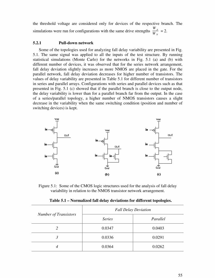
55
the threshold voltage are considered only for devices of the respective branch. The
simulations were run for configurations with the same drive strengths W p
W N
= 2.
5.2.1 Pull-down network
Some of the topologies used for analyzing fall delay variability are presented in Fig.5.1. The same signal was applied to all the inputs of the test structure. By runningstatistical simulations (Monte Carlo) for the networks in Fig. 5.1 (a) and (b) withdifferent number of devices, it was observed that for the series network arrangement,fall delay deviation slightly increases as more NMOS are placed in the gate. For theparallel network, fall delay deviation decreases for higher number of transistors. Thevalues of delay variability are presented in Table 5.1 for different number of transistorsin series and parallel arrays. Configurations with series and parallel devices such as thatpresented in Fig. 5.1 (c) showed that if the parallel branch is close to the output node,the delay variability is lower than for a parallel branch far from the output. In the caseof a series/parallel topology, a higher number of NMOS transistors causes a slightdecrease in the variability when the same switching condition (position and number ofswitching devices) is kept.
Figure 5.1: Some of the CMOS logic structures used for the analysis of fall delayvariability in relation to the NMOS transistor network arrangement.
Table 5.1 – Normalized fall delay deviations for different topologies.
Fall Delay DeviationNumber of Transistors
Series Parallel
2 0.0347 0.0403
3 0.0336 0.0291
4 0.0364 0.0262
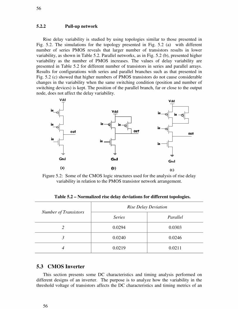
56
56
5.2.2 Pull-up network
Rise delay variability is studied by using topologies similar to those presented inFig. 5.2. The simulations for the topology presented in Fig. 5.2 (a) with differentnumber of series PMOS reveals that larger number of transistors results in lowervariability, as shown in Table 5.2. Parallel networks, as in Fig. 5.2 (b), presented highervariability as the number of PMOS increases. The values of delay variability arepresented in Table 5.2 for different number of transistors in series and parallel arrays.Results for configurations with series and parallel branches such as that presented inFig. 5.2 (c) showed that higher numbers of PMOS transistors do not cause considerablechanges in the variability when the same switching condition (position and number ofswitching devices) is kept. The position of the parallel branch, far or close to the outputnode, does not affect the delay variability.
Figure 5.2: Some of the CMOS logic structures used for the analysis of rise delayvariability in relation to the PMOS transistor network arrangement.
Table 5.2 – Normalized rise delay deviations for different topologies.
Rise Delay DeviationNumber of Transistors
Series Parallel
2 0.0294 0.0303
3 0.0240 0.0246
4 0.0219 0.0211
5.3 CMOS InverterThis section presents some DC characteristics and timing analysis performed on
different designs of an inverter. The purpose is to analyze how the variability in thethreshold voltage of transistors affects the DC characteristics and timing metrics of an
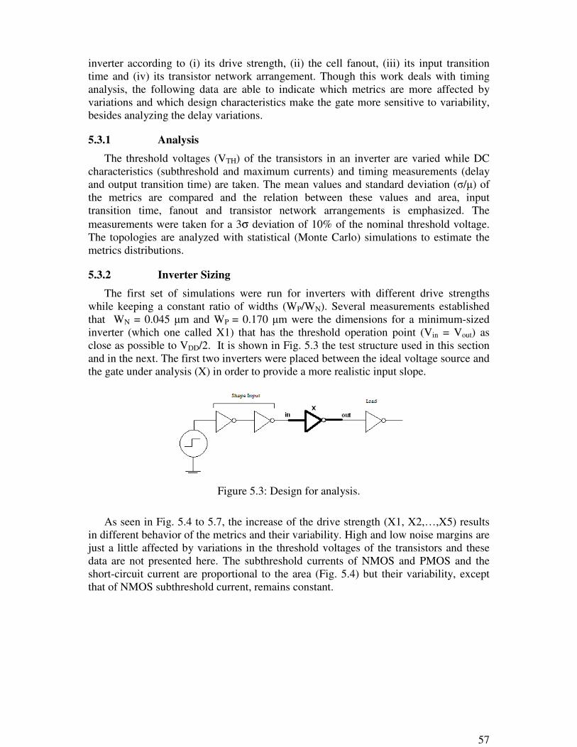
57
inverter according to (i) its drive strength, (ii) the cell fanout, (iii) its input transitiontime and (iv) its transistor network arrangement. Though this work deals with timinganalysis, the following data are able to indicate which metrics are more affected byvariations and which design characteristics make the gate more sensitive to variability,besides analyzing the delay variations.
5.3.1 Analysis
The threshold voltages (VTH) of the transistors in an inverter are varied while DCcharacteristics (subthreshold and maximum currents) and timing measurements (delayand output transition time) are taken. The mean values and standard deviation (σ/µ) ofthe metrics are compared and the relation between these values and area, inputtransition time, fanout and transistor network arrangements is emphasized. Themeasurements were taken for a 3σ deviation of 10% of the nominal threshold voltage.The topologies are analyzed with statistical (Monte Carlo) simulations to estimate themetrics distributions.
5.3.2 Inverter Sizing
The first set of simulations were run for inverters with different drive strengthswhile keeping a constant ratio of widths (WP/WN). Several measurements establishedthat WN = 0.045 µm and WP = 0.170 µm were the dimensions for a minimum-sizedinverter (which one called X1) that has the threshold operation point (Vin = Vout) asclose as possible to VDD/2. It is shown in Fig. 5.3 the test structure used in this sectionand in the next. The first two inverters were placed between the ideal voltage source andthe gate under analysis (X) in order to provide a more realistic input slope.
Figure 5.3: Design for analysis.
As seen in Fig. 5.4 to 5.7, the increase of the drive strength (X1, X2,…,X5) resultsin different behavior of the metrics and their variability. High and low noise margins arejust a little affected by variations in the threshold voltages of the transistors and thesedata are not presented here. The subthreshold currents of NMOS and PMOS and theshort-circuit current are proportional to the area (Fig. 5.4) but their variability, exceptthat of NMOS subthreshold current, remains constant.
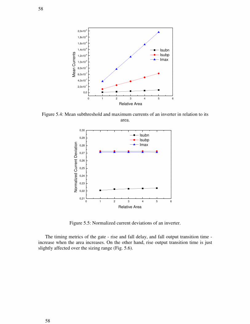
58
58
0 1 2 3 4 5 6
0,0
2,0x10⁻⁷
4,0x10⁻⁷
6,0x10⁻⁷
8,0x10⁻⁷
1,0x10⁻⁶
1,2x10⁻⁶
1,4x10⁻⁶
1,6x10⁻⁶
1,8x10⁻⁶
2,0x10⁻⁶
Me
an C
urr
ents
Relative Area
Isubn
Isubp
Imax
Figure 5.4: Mean subthreshold and maximum currents of an inverter in relation to itsarea.
0 1 2 3 4 5 60,21
0,22
0,23
0,24
0,25
0,26
0,27
0,28
0,29
0,30
Relative Area
Norm
aliz
ed C
urr
ent
De
via
tion
Isubn
Isubp
Imax
Figure 5.5: Normalized current deviations of an inverter.
The timing metrics of the gate - rise and fall delay, and fall output transition time -increase when the area increases. On the other hand, rise output transition time is justslightly affected over the sizing range (Fig. 5.6).

59
0 1 2 3 4 5 6
6,00E-011
8,00E-011
1,00E-010
1,20E-010
1,40E-010
1,60E-010
Me
an T
imin
g M
etr
ics
Relative Area
Rise Delay
Fall Delay
Rise Transition Time
Fall Transition Time
Figure 5.6: Timing metrics of an inverter in relation to its area.
It can be observed in Fig. 5.6 that the timing metrics directly related to the PMOStransistor – rise delay and rise output transition time – are less impacted by variations inthe area of the transistors than the metrics depending directly on the NMOS – fall delayand fall output transition time. Regarding timing metrics deviation, their behavior isdifferent from that of the mean values (Fig. 5.7). The larger the size of the inverter, thesmaller the rise and fall output slopes and the rise delay. Only the fall delay presentslarger deviation when the area increases. It means that falling transitions at the outputnode of inverters which are placed on the critical paths of the circuits are more criticalfor parametric yield and timing stability. Such information is quite useful for bufferinsertion tasks (JIANG, 1998), for instance.
0 1 2 3 4 5 6
0,015
0,020
0,025
0,030
0,035
0,040
0,045
0,050
0,055
0,060
0,065
0,070
No
rma
lize
d T
imin
g D
evia
tion
Relative Area
Rise Delay
Fall Delay
Rise Transition Time
Fall Transition Time
Figure 5.7: Normalized timing metrics deviation of an inverter in relation to thetransistors areas.

60
60
The methodology used in the work considered the same threshold voltage variation(± 10%) independently on the size of the gate. Therefore, our purpose was to analyzehow size (drive strength) affects currents and timing variability once a specific variationtakes place.
5.3.3 Output Load
The influence of the fanout on the variability of the metrics is also studied. Thefanout was represented by an inverter with a range of area from one to eight times thesize of the driver inverter. The subthreshold and short-circuit currents, the noise marginsvalues, and also their variability, are practically not affected by the different fanoutsused in the simulations. However, as the fanout increases, the mean values of all of thetiming measurements also increases, as in Fig. 5.8.
0 1 2 3 4 5 6 7 8 92,00E-011
4,00E-011
6,00E-011
8,00E-011
1,00E-010
1,20E-010
1,40E-010
MeanT
imin
g M
etr
ics
Relative Fanout
Rise Delay
Fall Delay
Rise Transition Time
Fall Transition Time
Figure 5.8: Timing metrics of inverter in relation to the output load.
The rise and fall transition times at the output node are more affected by changes inthe fanout than the rise and fall delays. The normalized fall delay deviation is kind of ahyperbolic function of the fanout – as it increases, the deviation decreases (Fig. 5.9).The deviations of the other metrics increases in a quasi-linear rate, but themeasurements for a falling-edge at the output are more sensitive to changes in thefanout of the gate. For a fanout cell with area between 5 and 6 times the minimum-sizedinverter there is a point of intersection in the curves of delay deviations, that could beused as information to design gates with reasonable values for both delays.

61
0 1 2 3 4 5 6 7 8 9
0,020
0,025
0,030
0,035
0,040
0,045
0,050
0,055
0,060
No
rma
lize
d T
imin
g D
evia
tio
n
Relative Fanout
Rise Delay
Fall Delay
Rise Transition Time
Fall Transition Time
Figure 5.9: Normalized timing metrics deviation of an inverter in relation to the outputload.
5.3.4 Input Transition Time
Inverters with different areas were placed at the input of inverter on which themeasurements are being performed in order to change the transition time of the inputsignal. In Fig. 5.10, the input gate that contributes with the input capacitance is calledX1 to X5, depending on its size relatively to the size of the main gate, called X1 (WN =0.045 µm and WP = 0.170 µm).
Figure 5.10: Topology using an auxiliary inverter (X1…X5) connected to the input ofthe main inverter for changing the input slope.
Fig. 5.11 and 5.12 present the results for the mean timing metrics and theirdeviations. The mean delays and output transition times are proportional to the size ofthe auxiliary inverter, what means that these metrics increase as the input slopeincreases. Regarding deviations, only the fall delay presents higher deviations for largercapacitances connected to the input. Rise delay deviation is practically constant and riseoutput transition time deviation decreases. The fall output transition time deviation hasan interesting behavior, being a convex function of the size of the auxiliary inverter witha minimum value when it is sized as X3 (WN = 0.135 µm and WP = 0.510 µm).

62
62
0 1 2 3 4 5 6
6,00E-011
8,00E-011
1,00E-010
1,20E-010
1,40E-010
1,60E-010
1,80E-010
2,00E-010
2,20E-010
Avera
ge T
imin
g M
etr
ics
Relative Fanin
Rise Delay
Fall Delay
Rise Transition Time
Fall Transition Time
Figure 5.11: Timing metrics of an inverter in relation to the input capacitance.
0 1 2 3 4 5 6
0,00
0,01
0,02
0,03
0,04
0,05
0,06
0,07
No
rma
lize
d T
imin
g D
evia
tio
n
Relative Fanin
Rise Delay
Fall Delay
Rise Transition Time
Fall Transition Time
Figure 5.12: Normalized timing metrics deviation of an inverter in relation to the inputcapacitance.
5.3.5 Transistor Network Arrangements
Fig. 5.13 shows different topologies for an inverter keeping constant the ratio(WP/WN) and the drive strength of the pull-up and pull-down networks. The topology inFig. 5.13(b), that represents the split of transistors in larger series ones, is commonlyused for subthreshold leakage current saving. Fig. 5.13(c) represents a layoutoptimization technique called folding, that splits a transistor in smaller parallel ones.The comparison among the topologies showed that a series configuration of transistorsresults in lower delay variability for the currents analyzed, the delays and the outputtransition times.
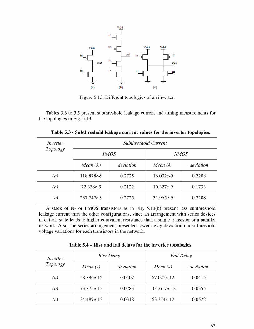
63
Figure 5.13: Different topologies of an inverter.
Tables 5.3 to 5.5 present subthreshold leakage current and timing measurements forthe topologies in Fig. 5.13.
Table 5.3 - Subthreshold leakage current values for the inverter topologies.
Subthreshold Current
PMOS NMOS
Inverter
Topology
Mean (A) deviation Mean (A) deviation
(a) 118.878e-9 0.2725 16.002e-9 0.2208
(b) 72.338e-9 0.2122 10.327e-9 0.1733
(c) 237.747e-9 0.2725 31.965e-9 0.2208
A stack of N- or PMOS transistors as in Fig. 5.13(b) present less subthresholdleakage current than the other configurations, since an arrangement with series devicesin cut-off state leads to higher equivalent resistance than a single transistor or a parallelnetwork. Also, the series arrangement presented lower delay deviation under thresholdvoltage variations for each transistors in the network.
Table 5.4 – Rise and fall delays for the inverter topologies.
Rise Delay Fall DelayInverter
TopologyMean (s) deviation Mean (s) deviation
(a) 58.896e-12 0.0407 67.025e-12 0.0415
(b) 73.875e-12 0.0283 104.617e-12 0.0355
(c) 34.489e-12 0.0318 63.374e-12 0.0522

64
64
Rise and fall delay variability is also lower for the series transistors configuration,but their mean values are the highest among the topologies presented. The samesituation takes place for the rise and fall transition times, as presented in Table 5.5.
Table 5.5 - Rise and fall transition times for the inverter topologies.
Timing
Rise Transition Fall Transition
Inverter
Topology
Mean (s) deviation Mean (s) deviation
(a) 90.603e-12 0.0347 103.084e-12 0.0243
(b) 114.074e-12 0.0250 123.923e-12 0.0138
(c) 93.183e-12 0.0344 118.415e-12 0.0218
Fig. 5.14 presents another folding design in which the inverter is divided into largernumber of parallel transistors. This topology has the lowest delay variability among allpresented so far.
Figure 5.14: Folding topology of an inverter.
Successive folding seems a good technique when the goal is to control delayvariability. However, the threshold voltage variations of the transistors were keeptconstant in the methodology here applied, independently on the new sizes transistorsacquire in the folding technique. This point is a limitation of the analysis, since thePelgrom model describes the threshold voltage as an inverse function of the are oftransistors. So, larger devices have lower VTH variations and that can compensate someof the advantage presented by the use of a higher number of smaller devices. Furtheranalysis on this subject will be performed on CHAPTER 7.
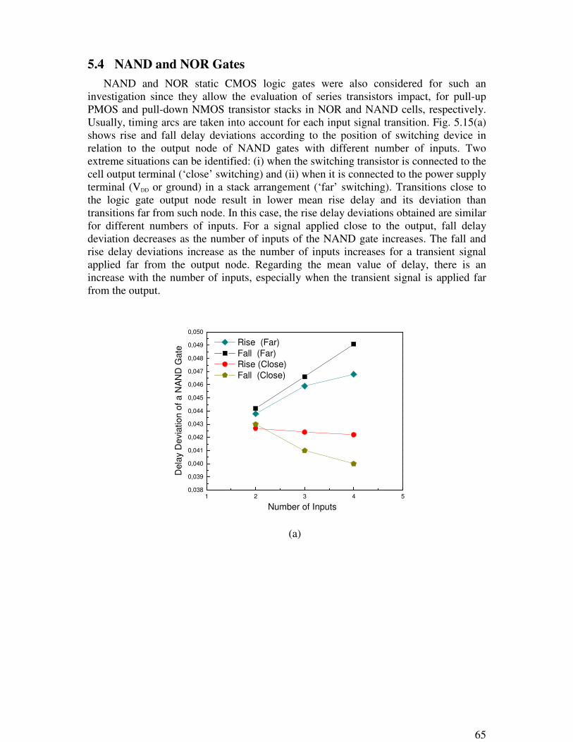
65
5.4 NAND and NOR GatesNAND and NOR static CMOS logic gates were also considered for such an
investigation since they allow the evaluation of series transistors impact, for pull-upPMOS and pull-down NMOS transistor stacks in NOR and NAND cells, respectively.Usually, timing arcs are taken into account for each input signal transition. Fig. 5.15(a)shows rise and fall delay deviations according to the position of switching device inrelation to the output node of NAND gates with different number of inputs. Twoextreme situations can be identified: (i) when the switching transistor is connected to thecell output terminal (‘close’ switching) and (ii) when it is connected to the power supplyterminal (VDD or ground) in a stack arrangement (‘far’ switching). Transitions close tothe logic gate output node result in lower mean rise delay and its deviation thantransitions far from such node. In this case, the rise delay deviations obtained are similarfor different numbers of inputs. For a signal applied close to the output, fall delaydeviation decreases as the number of inputs of the NAND gate increases. The fall andrise delay deviations increase as the number of inputs increases for a transient signalapplied far from the output node. Regarding the mean value of delay, there is anincrease with the number of inputs, especially when the transient signal is applied farfrom the output.
1 2 3 4 50,038
0,039
0,040
0,041
0,042
0,043
0,044
0,045
0,046
0,047
0,048
0,049
0,050
Number of Inputs
Dela
y D
evia
tion o
f a N
AN
D G
ate
Rise (Far)
Fall (Far)
Rise (Close)
Fall (Close)
(a)
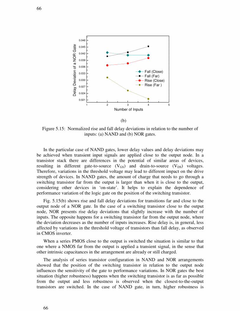
66
66
1 2 3 4 5
0.021
0.024
0.027
0.030
0.033
0.036
0.039
0.042
0.045
0.048
Number of Inputs
Dela
y D
evia
tion o
f a N
OR
Gate
Fall (Close)
Fall (Far)
Rise (Close)
Rise (Far )
(b)
Figure 5.15: Normalized rise and fall delay deviations in relation to the number ofinputs: (a) NAND and (b) NOR gates.
In the particular case of NAND gates, lower delay values and delay deviations maybe achieved when transient input signals are applied close to the output node. In atransistor stack there are differences in the potential of similar areas of devices,resulting in different gate-to-source (VGS) and drain-to-source (VDS) voltages.Therefore, variations in the threshold voltage may lead to different impact on the drivestrength of devices. In NAND gates, the amount of charge that needs to go through aswitching transistor far from the output is larger than when it is close to the output,considering other devices in ‘on-state’. It helps to explain the dependence ofperformance variation of the logic gate on the position of the switching transistor.
Fig. 5.15(b) shows rise and fall delay deviations for transitions far and close to theoutput node of a NOR gate. In the case of a switching transistor close to the outputnode, NOR presents rise delay deviations that slightly increase with the number ofinputs. The opposite happens for a switching transistor far from the output node, wherethe deviation decreases as the number of inputs increases. Rise delay is, in general, lessaffected by variations in the threshold voltage of transistors than fall delay, as observedin CMOS inverter.
When a series PMOS close to the output is switched the situation is similar to thatone where a NMOS far from the output is applied a transient signal, in the sense thatother intrinsic capacitances in the arrangement are already or still charged.
The analysis of series transistor configuration in NAND and NOR arrangementsshowed that the position of the switching transistor in relation to the output nodeinfluences the sensitivity of the gate to performance variations. In NOR gates the bestsituation (higher robustness) happens when the switching transistor is as far as possiblefrom the output and less robustness is observed when the closest-to-the-outputtransistors are switched. In the case of NAND gate, in turn, higher robustness is

67
achieved by applying the transient signal close to the output node. The results forvariations of delay are not the same as the results for the absolute delay value. It is wellknown that a better timing (lower delay) is achieved when a critical path signal iscrossing through the switching device closer to the logic gate output node. A trade-off isrequired since it is not interesting to have the timing of the cell with a high mean valueeven though it presents low variability.
Rising- and falling-edge output signals go through essentially different paths inNAND and NOR gates. In the former, series transistors are in pull-down NMOSnetwork and they are responsible for a falling-edge output signal. On the other hand, inthe latter, series transistors are in pull-up PMOS network and are responsible for arising-edge output. The comparison between the influences of the variations in theparameters on NOR and NAND delays are physically more appropriate by consideringequivalent array of transistors: series-to-series or parallel-to-parallel. In this case, thefall delay variations of NAND gate may be compared to the rise delay variations ofNOR gate, and vice-versa. Fig. 5.16 shows delay deviations for transitions far and closeto the output node for NAND and NOR gates in stacked transistors. For both situations,NAND gates are more sensitive to variations in transistor threshold voltage than NORgates.
1 2 3 4 5
0,021
0,024
0,027
0,030
0,033
0,036
0,039
0,042
0,045
0,048
Dela
y D
evia
tion
Number of Inputs
NOR (far)
NAND (far)
NOR (close)
NAND (close)
Figure 5.16: Comparison of NMOS and PMOS transistor stacking in NAND and NORgates, respectively, for different positions of the switching device (‘close’ to and ‘far’
from output node).
By analyzing the sensitivity of basic gates to VTH variations, some tendencies wereobserved in the deviations of their delay due to transistor network structure and theposition of the switching transistor in relation to the output node. Such analysis cannotconclude that NAND and NOR gates with fewer inputs would be the best or the worstchoice, once opposite behavior of delay deviation is observed according to the positionof the switching device in the network. On the other hand, in critical paths optimization,by switching transistors closer to the gate output node tends to provide betterperformance in terms of absolute delay as well as parametric yield improvement.

68
68
5.5 NAND: Single Gate Versus Mapped CircuitWhile evaluating topologies with different number of inputs a question arose: would
it be better, in terms of variability, to replace a single complex gate with large numberof inputs by a circuit mapped to basic gates with fewer inputs, in order to implement thesame logic function? Fig. 5.17 illustrates how it could be done in the case of a 3-inputNAND gate. Table 5.6 presents the results obtained for a single 3-input NAND gate(‘NAND3’) and a version composed with two 2-input NAND gates (‘2xNAND2’). Thiscase was investigated considering only one transistor switching at a time, and the fastestand the slowest paths were identified.
Figure 5.17: Illustration of single 3-input NAND gate implemented by using two 2-input NAND gates (‘2xNAND2’).
Table 5.6: Delay deviation of the shortest and the longest paths in Fig. 5.17.
Best-case delay Worst-case delay
2xNAND2 NAND3 2xNAND2 NAND3
Mean Rise Delay (ps) 87.99 82.39 153.93 141.30
Norm. Rise Delay Deviation 0.0446 0.0424 0.0293 0.0457
Mean Fall Delay (ps) 83.42 48.75 163.18 67.85
Norm. Fall Delay Deviation 0.0339 0.0466 0.0243 0.0410
The single 3-input NAND gate is more sensitive to variations of transistor thresholdvoltage than the version composed by two 2-input NAND gates for the slowest signalpropagation (worst-case), since variations in the threshold voltage of a 3-input NANDresulted in higher delay deviation than in the case when two 2-input NAND gates (withadditional inverter) were used. For the fastest propagation (best-case) it is notcompletely so. Though fall delay deviation is higher for NAND3, rise delay deviation isalmost the same for both configurations. Also, the NAND3 is much faster than theimplementation with 2-input NAND gates for a falling-edge at the output node. Theresults shown in Table 5.6 agree well with Fig. 5.15a for rise delay deviation, once it isnot really affected by the number of input signals in the logic gate.
A more complete analysis is possible by the probability density functions (PDF) ofdelay for both topologies, as presented in Fig. 5.18. Though NAND03 is more sensitiveto variations in VTH, the PDF of rise and fall delays for the longest and the shortestpaths show that this gate guarantees faster signal propagation for almost every variationin VTH.
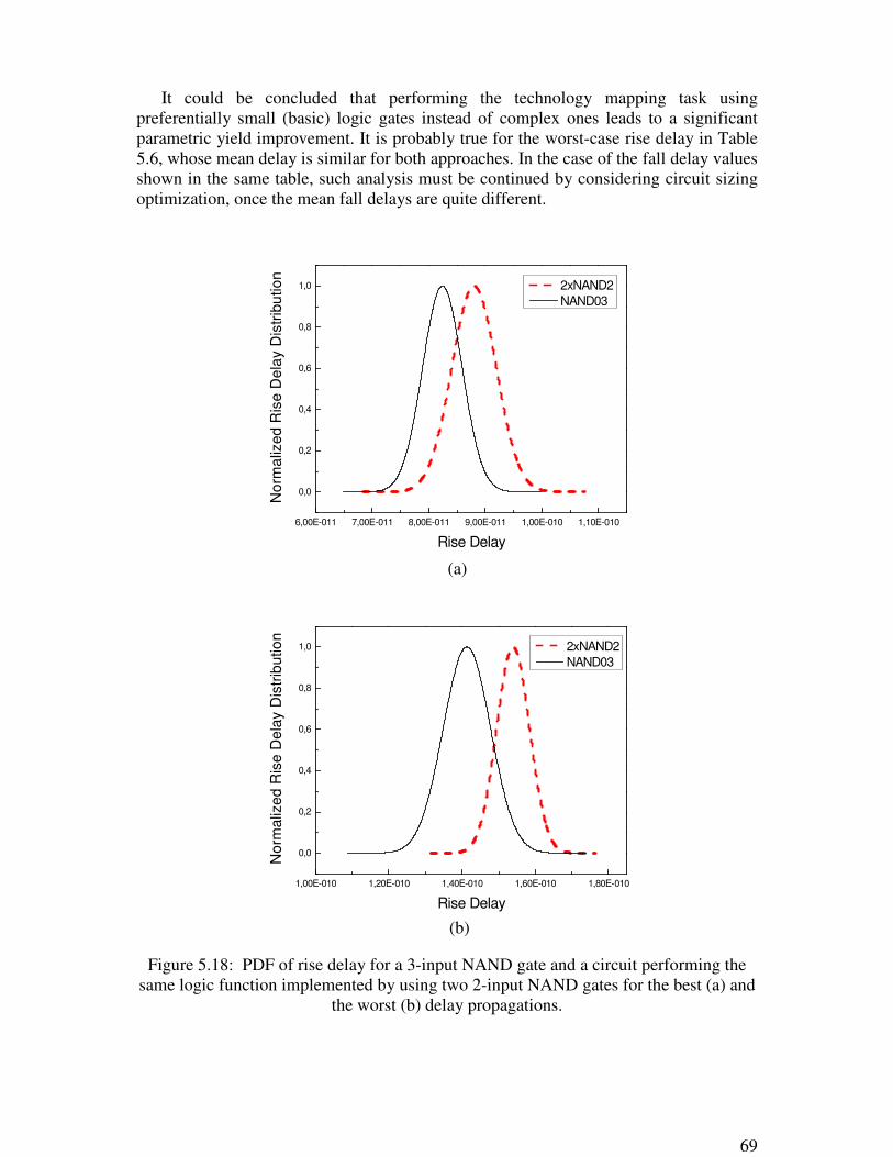
69
It could be concluded that performing the technology mapping task usingpreferentially small (basic) logic gates instead of complex ones leads to a significantparametric yield improvement. It is probably true for the worst-case rise delay in Table5.6, whose mean delay is similar for both approaches. In the case of the fall delay valuesshown in the same table, such analysis must be continued by considering circuit sizingoptimization, once the mean fall delays are quite different.
6,00E-011 7,00E-011 8,00E-011 9,00E-011 1,00E-010 1,10E-010
0,0
0,2
0,4
0,6
0,8
1,0
No
rma
lized R
ise D
ela
y D
istr
ibu
tion
Rise Delay
2xNAND2
NAND03
(a)
1,00E-010 1,20E-010 1,40E-010 1,60E-010 1,80E-010
0,0
0,2
0,4
0,6
0,8
1,0
Norm
aliz
ed R
ise D
ela
y D
istr
ibutio
n
Rise Delay
2xNAND2
NAND03
(b)
Figure 5.18: PDF of rise delay for a 3-input NAND gate and a circuit performing thesame logic function implemented by using two 2-input NAND gates for the best (a) and
the worst (b) delay propagations.
70
70
5.6 And-Or-Inverter (AOI) Logic GatesPrevious analysis, taking into account separately pull-down NMOS and pull-up
PMOS logic networks, has demonstrated that the lower device count is present in atransistor arrangement, the less sensitive it is to threshold voltage variations. And-Or-Inverter configurations (AOI_21 and AOI_32) were implemented in two versions: (i) asa single CMOS complex gate and (ii) by using basic cells (2-input NAND and NORgates). These topologies provide mixed arrangements of series and parallel transistors inthe pull-up PMOS and pull-down NMOS networks. The goal is to evaluate if suchimplementation becomes more susceptible to variations than the same logic functionmapped with basic gates.
The implementation of AOI_21 by considering basic gates presented lower delaydeviations, but higher mean fall delay in comparison to the single complex gateapproach. Similar situation has been observed for AOI_32 implementation. The resultsare summarized in Table 5.7. Fig. 5.19 illustrates the rise delay distributions for bothtopologies.
Table 5.7: Delay deviation for AOI_21 and AOI_32 logic gates.
AOI-21 AOI-32Metrics
Complex
gate
Basic gates Complex
gate
Basic gates
Mean Rise Delay (ps) 166.39 157.73 212.84 152.38
Norm. Rise Delay Deviation 0.0331 0.0240 0.0339 0.0284
Mean Fall Delay (ps) 52.64 126.97 103.78 172.45
Norm. Fall Delay Deviation 0.0465 0.0188 0.0395 0.0303

71
1,40E-010 1,50E-010 1,60E-010 1,70E-010 1,80E-010 1,90E-010 2,00E-010
0,0
0,2
0,4
0,6
0,8
1,0
Norm
aliz
ed
Ris
e D
ela
y D
istr
ibu
tio
n
Rise Delay
Basic Gates
Complex Gate
(a)
1,50E-010 1,80E-010 2,10E-010 2,40E-010 2,70E-010
0,0
0,2
0,4
0,6
0,8
1,0
1,2
Norm
aliz
ed R
ise
Dela
y D
istr
ibutio
n
Rise Delay
Basic Gates
Complex Gate
(b)
Figure 5.19: PDF of rise delay for AOI_21 (a) and AOI_32 (b) gates implemented byusing basic CMOS cells and as a single complex gate.
The implementation with basic gates was able to reduce the overall delay of anAOI_32 configuration and guaranteed more reliability for changes in transistorsthreshold voltages. It suggests that complex implementations presenting a larger numberof series and parallel transistors in the cell topology may reduce the mean delay value atexpense of increasing the performance variability. Circuit sizing was not considered forperformance optimization, being all gates sized for similar drive strength.
In these last experiments by considering AOI logic gates, the results and analysis aresimilar to the ones discussed in the previous section. The mapped circuits, based onsmall cells, provide better performance in terms of delay variability. The values

72
72
presented in Table 5.5 suggest lower normalized delay deviations for ‘basic gates’approach in both cases when the mean delay does not present the same tendency, asobserved in the AOI_32 results. It reinforces the design guideline that suggests the useof small (basic) gates as preferential choice in the technology mapping task whenparametric yield improvement is targeted.
5.7 ConclusionResults obtained in this work so far about performance variability in CMOS logic
gates submitted to transistor threshold voltage variation demonstrated the strongdependency it has on the gate topology, the number of stacked transistors, and therelative position of switching device in transistor network arrangements. Such analysissuggests the preferential use of basic CMOS gates instead of complex ones (AOI, forinstance) in the technology mapping task of combinational circuits. Moreover, in termsof critical delay paths optimization, switching transistors placed close to the gateoutputs are preferable for absolute delay propagation. Also, the results presented for theinverter gate showed that not only its performance, but also its DC characteristics areaffected by variations in the threshold voltage of transistors. In a gate-level analysis itis also essential to study the condition of the input signal (input slope) and the loadcell(s) since they also affects variability. Some changes in the transistor network can bedone to reduce variability, like folding. The analysis performed in this work can beextended to other logic gates.

73
6 DELAY VARIABILITY ESTIMATION METHOD
Fluctuations of devices characteristics are very pronounced in deep submicrontechnology. As a consequence, it is necessary to take transistors characteristicsvariability into account in order to properly calculate the delay of a logic cell.
The present work proposes the implementation of a method that can predict thedelay variability of a logic gate. It is performed here by assigning a unique variable –the threshold voltage variation – to each transistor in the analyzed logic gate. Wheneverpossible, the gate is divided into pull-up and pull-down networks, what reduces thenumber of devices and variables one must deal with.
Factorial designs (MYERS, 2002) are used to identify the main effects of the factors(∆VTH) on the primarily targeted variable, the transistors ‘on-resistance’. Since eachvariable of interest is given by two levels (the coded values –1 and +1), each variant ofsuch a design has 2k experimental runs being called a 2k factorial design, where ‘k’ isthe number of transistors in the gate under test (i.e.,‘k’ threshold voltage values). As anexample, Table 6.1 shows factorial values when a network with three transistors isconsidered. The values correspond to those used in the runs with HSPICE in order tofind the resistances for each corner, with the difference that the threshold voltages in thenetlist files have their natural (non-coded) values for performing the simulations.
Table 6.1: Combinations of min and max values considered for the thresholdvoltages variations (coded variables) of devices in a 3-transistors network .
Corners ∆Vth3
∆Vth2
∆Vth1
1 -1 -1 -12 -1 -1 13 -1 1 -14 -1 1 15 1 -1 -16 1 -1 17 1 1 -18 1 1 1
Fig. 6.1 presents graphically the combinations of min and max coded valuesconsidered for the threshold voltages variations of devices in a 3-transistors network.Since in this example there are 3 transistors, the number of runs is 23.
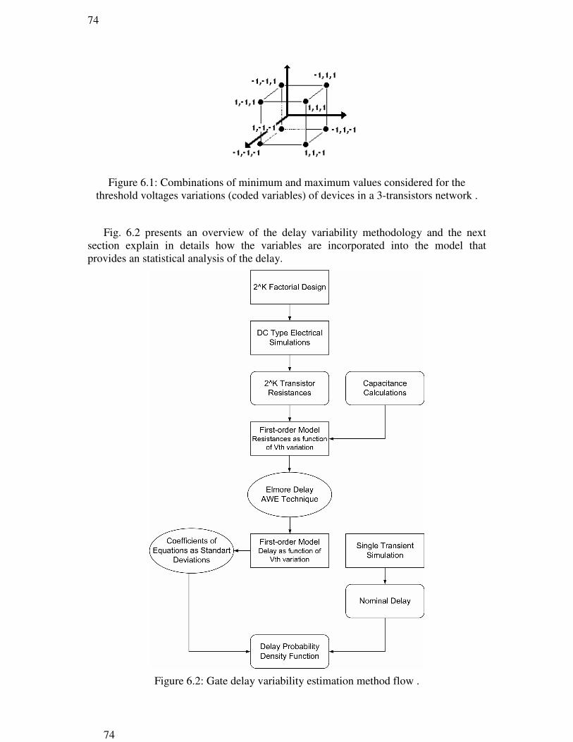
74
74
Figure 6.1: Combinations of minimum and maximum values considered for thethreshold voltages variations (coded variables) of devices in a 3-transistors network .
Fig. 6.2 presents an overview of the delay variability methodology and the nextsection explain in details how the variables are incorporated into the model thatprovides an statistical analysis of the delay.
Figure 6.2: Gate delay variability estimation method flow .

75
Initially, DC type electrical simulations extract the ‘on-resistances’ of transistors fordifferent threshold voltages (VTH) in a corner-based principle. The VTH of transistors arevaried ±10% of their nominal values and transformed into coded (normalized) variableswith values –1 and +1, which represent the minimum and maximum values assumed byVTH, respectively.
The effect estimated in a 2K factorial design is then converted into a regressionmodel (first-order function for the resistance of the device) that can be used to analyzethe response at any point in the space spanned by the factors (coded ∆VTH) in thedesign. For the example presented in Table 6.1, the resistances are provided by 23 (threetransistors) DC simulation with HSPICE, by dividing the voltage drop in each transistorby the current through it.
Linear regression technique is next used to develop approximate models for theresistances of transistors in different states as function of ∆VTH of all the devices in thenetwork. The dynamic response of a MOS is a function of the time. It takes into accountthe charging and discharging of parasitic capacitances that are intrinsic to the device,and the capacitances introduced by the interconnect lines and the load. The intrinsiccapacitances originate from three sources: the basic MOS structure, the channel charge,and the depletion regions of the reversed-biased pn-junction of transistor drain andsource regions (RABAEY, 2005). The intrinsic capacitances are calculated for specifictechnology nodes and are considered as constants in the proposed method. The delay iscalculated through the RC constant of the network by using again factorial design. Afirst-order regression model represents the delay as a function of the coded ∆VTH.
Two different methods have been used to calculate the delay variation for thetransistors networks, the Elmore Delay model (ELMORE, 1948) and the AsymptoticWaveform Evaluation technique (AWE) (PILLAGE, 1990). The resistance equationsobtained in the first step are used to perform the following analysis. The thresholdvoltages variations of the transistors are considered as random variables represented byprobability density functions (PDF) with mean values equal to zero and normalizedstandard deviations [N(0,1)]. Since the VTH variations are treated as coded variables, thecoeficients of the final delay equation is considered as the standard deviation (σ)resulting from each VTH variation. It is then performed a sum of normal distributions,and the result is a PDF that represents the delay of the network with the two aspectsconsidered: mean and standard deviation (square root of variance). The normalizedstandard deviation (standard deviation divided by the mean) of the delay is the focus ofthe analysis of different networks, because it makes possible to compare the variabilityof arrangements with different mean delays.
6.1 On-ResistanceQualitatively, a MOS transistor can be modeled as a switch with a finite on-
resistance RON (RABAEY, 2005). When the voltage between the gate and the source(VGS) is lower than the threshold voltage (VTH), the switch is considered open. WhenVGS is higher than VTH, the transistor behaves as a finite resistance. This resistance isnot constant and changes according to the region of operation of the transistors, whichalso depends on the difference of potential between drain and source (VDS). The on-resistance of an MOS transistor depends upon its operation point and varies during theswitching transient. Though the use of a linear constant resistance may introduce someerror in the performance calculations, the use of a fixed RON might be a reasonable
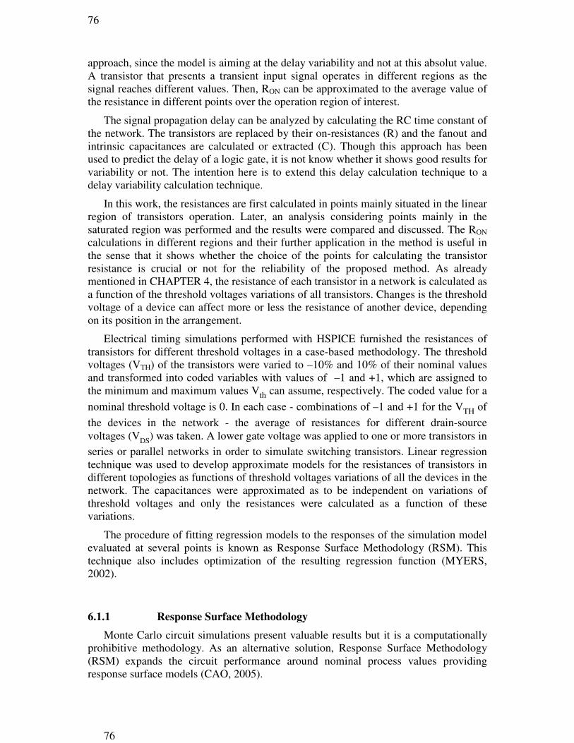
76
76
approach, since the model is aiming at the delay variability and not at this absolut value.A transistor that presents a transient input signal operates in different regions as thesignal reaches different values. Then, RON can be approximated to the average value ofthe resistance in different points over the operation region of interest.
The signal propagation delay can be analyzed by calculating the RC time constant ofthe network. The transistors are replaced by their on-resistances (R) and the fanout andintrinsic capacitances are calculated or extracted (C). Though this approach has beenused to predict the delay of a logic gate, it is not know whether it shows good results forvariability or not. The intention here is to extend this delay calculation technique to adelay variability calculation technique.
In this work, the resistances are first calculated in points mainly situated in the linearregion of transistors operation. Later, an analysis considering points mainly in thesaturated region was performed and the results were compared and discussed. The RON
calculations in different regions and their further application in the method is useful inthe sense that it shows whether the choice of the points for calculating the transistorresistance is crucial or not for the reliability of the proposed method. As alreadymentioned in CHAPTER 4, the resistance of each transistor in a network is calculated asa function of the threshold voltages variations of all transistors. Changes is the thresholdvoltage of a device can affect more or less the resistance of another device, dependingon its position in the arrangement.
Electrical timing simulations performed with HSPICE furnished the resistances oftransistors for different threshold voltages in a case-based methodology. The thresholdvoltages (VTH) of the transistors were varied to –10% and 10% of their nominal valuesand transformed into coded variables with values of –1 and +1, which are assigned tothe minimum and maximum values Vth can assume, respectively. The coded value for a
nominal threshold voltage is 0. In each case - combinations of –1 and +1 for the VTH of
the devices in the network - the average of resistances for different drain-sourcevoltages (VDS) was taken. A lower gate voltage was applied to one or more transistors in
series or parallel networks in order to simulate switching transistors. Linear regressiontechnique was used to develop approximate models for the resistances of transistors indifferent topologies as functions of threshold voltages variations of all the devices in thenetwork. The capacitances were approximated as to be independent on variations ofthreshold voltages and only the resistances were calculated as a function of thesevariations.
The procedure of fitting regression models to the responses of the simulation modelevaluated at several points is known as Response Surface Methodology (RSM). Thistechnique also includes optimization of the resulting regression function (MYERS,2002).
6.1.1 Response Surface Methodology
Monte Carlo circuit simulations present valuable results but it is a computationallyprohibitive methodology. As an alternative solution, Response Surface Methodology(RSM) expands the circuit performance around nominal process values providingresponse surface models (CAO, 2005).

77
RSM explores the relation between the independent (input) variables and one ormore response variables, represented, in this work, by the performance metrics: rise andfall delays of the logic gates. The form of the true response function f is unknown andsometimes very complicated, so it is necessary to approximate it (MYERS, 2002). Therelation between the response y and the independent variables ξ1, ξ2,..., ξk is:
y = f(ξ1, ξ2,..., ξk) + ε(6.1)
where ε is the term that represents sources of variability not accounted for in thefunction f, such as measurement errors, background noise etc. The variables ξ1, ξ2,..., ξk
are called the “natural variables” because they are expressed in the natural units ofmeasurements, such as degrees Celsius, grams per liter etc. That can be convenient totransform the natural variables into “coded variables” x1, x2,..., xk, which are usuallydefined to be dimensionless with mean zero and the same standard deviation. By usingcoded variables, the response function will be written as:
η = f(x1, x2,..., xk)(6.2)
The order of the model that will represent the response depends on the region of theindependent variable space over which the true response surface is approximated. Forthe case of three independent variables (there is no interaction between them), aspresented before, the first-order model in terms of the coded variable is:
η = β0 + β1.x1 + β2.x2 + β3.x3(6.3)
where the β’s are the coefficients resulting from the fitting. This first-order model issometimes called a main effects model, since it includes only the main effects of thevariables.
(OKADA, 2003) uses RSM to propose a model that characterizes a statistical gatedelay variation. Coefficients of RSM are derived from several SPICE simulations byusing a least square method.
6.2 MOS Structures CapacitancesThe dynamic response of a MOS is a function of the time it takes to charge and
discharge the parasitic capacitances that are intrinsic to the device, and the extracapacitances introduced by the interconnect lines and the load. The intrinsiccapacitances originate from three sources: the basic MOS structure, the channel charge,and the depletion regions of the reversed-biased pn-junctions of drain and source(RABAEY, 2005), represented by the intrinsic diodes in Fig. 6.3b.

78
78
(a) (b)
Figure 6.3: Intrinsic capacitances of a MOS transistor.
6.2.1 Gate Capacitance
6.2.1.1 Channel Capacitance
The gate of the MOS transistor is isolated from the conducting channel by the gateoxide and its capacitance per unit area is equal to:
Coxox
toxn (6.4)
The total channel capacitance is calculated by multiplying the value above and thegate area:
Cgnox
toxnWn Ln
(6.5)
in which Wn is the width and Ln is the length of the channel for a NMOS transistor.
Cgpox
toxpWp Lp
(6.6)
in which Wp is the width and Lp is the length of the channel for a PMOS transistor.
The gate-to-channel capacitance (CGC
) depends upon the operation region and
terminal voltages of the transistor. It is divided into three components: gate-to-source(C
GCS), gate-to-drain (C
GCD) and gate-to-body (C
GCB) capacitances. In the cut-off region,
no channel is formed and the total gate-to-channel capacitance appears between gateand body:
CGCBox
toxnWn Ln
(6.7)
In the resistive (linear) region, the gate capacitance distributes evenly betweensource and drain, as the body electrode is shielded from the gate by the channel:
CGCS CGCD
1
2
ox
toxnWn Ln
(6.8)

79
In the saturation mode, the capacitance between gate and drain and the gate-bodycapacitance are approximately zero. All the capacitance is therefore between gate andsource:
CGCS
2
3
ox
toxnWn Ln
(6.9)
6.2.1.2 Overlap Capacitance
In reality, source and drain diffusion are not entirely performed along only onedirection inside the semiconductor and tend to extend a little below the oxide by anamount xd, what characterizes a lateral diffusion of the ions implanted. It gives rise to a
parasitic capacitance between gate and source (drain) that is called overlap capacitanceand it has a fixed value (per unit area). These capacitances are given by:
Cgdn = Cgdo * Wn for the NMOS transistor; (6.10)
Cgdp = Cgdo * Wp for the PMOS transistor; (6.11)
in which Cgdo is the gate-drain capacitance per unit area. Fig. 6.3 shows thesecapacitances as Cgs and Cgd.
The overlap capacitances between gate and source are calculated in the same way asabove, changing Cgdo by Cgso. In the proposed method, the source diffusion capacitancesof the transistors connected to the power lines are not included in the calculations, sincethey are considered permanently charged or discharged.
6.2.2 Junction Capacitances
A capacitive component is contributed by the reverse-biased source-bulk and drain-bulk pn-junctions.
6.2.2.1 Bottom-Plate Junction Capacitance
This capacitance appears because of the depletion layer between the drain region(with doping N
D for NMOS and N
A for PMOS) and the substrate with doping N
A
(NMOS) or ND (PMOS). The total depletion region capacitance for this component
equals:
Cdbn = Cjn * Wn * Ldn for the NMOS transistor; (6.12)
where Cjn is the junction bottom capacitance per unit area for the NMOS transistor andLdn is the drain region length.
C jn
C jo
1Vbsn
j
MJ
(6.13)

80
80
where Cjo represents the zero-bias junction capacitance per unit area and MJ is a
grading coefficient. φj represents the difference in the internal chemical potentials
between the n and p sides of the junction.
j
K T
qln
NA ND
ni2
(6.14)
where ni represents the intrinsic carrier concentration.
Cdbp = Cjp * Wp * Ldp for the PMOS transistor; (6.15)
where Cjp is the junction bottom capacitance per unit area for the PMOS transistor
C jp
C jo
1Vbsp
j
MJ
(6.16)
6.2.2.2 Side-Wall Junction Capacitance
This capacitance is counted for the sides of drain and source region, but not for theside where the conductive channel is placed.
Cswdn Csjwn 2 Ldn Wn (6.17)
Cswdp Csjwp 2 Ldp Wp (6.18)
6.2.3 The Inverter
The inverter is the nucleus of digital designs and once its operation and propertiesare understood, it gets simpler to design more intricate structures. Fig. 6.4 presents theeletrical diagram of a inverter and Fig. 6.5 shows the diagram of a CMOS invertermodeled as an RC circuit.
Figure 6.4: CMOS Inverter (RABAEY, 2005).
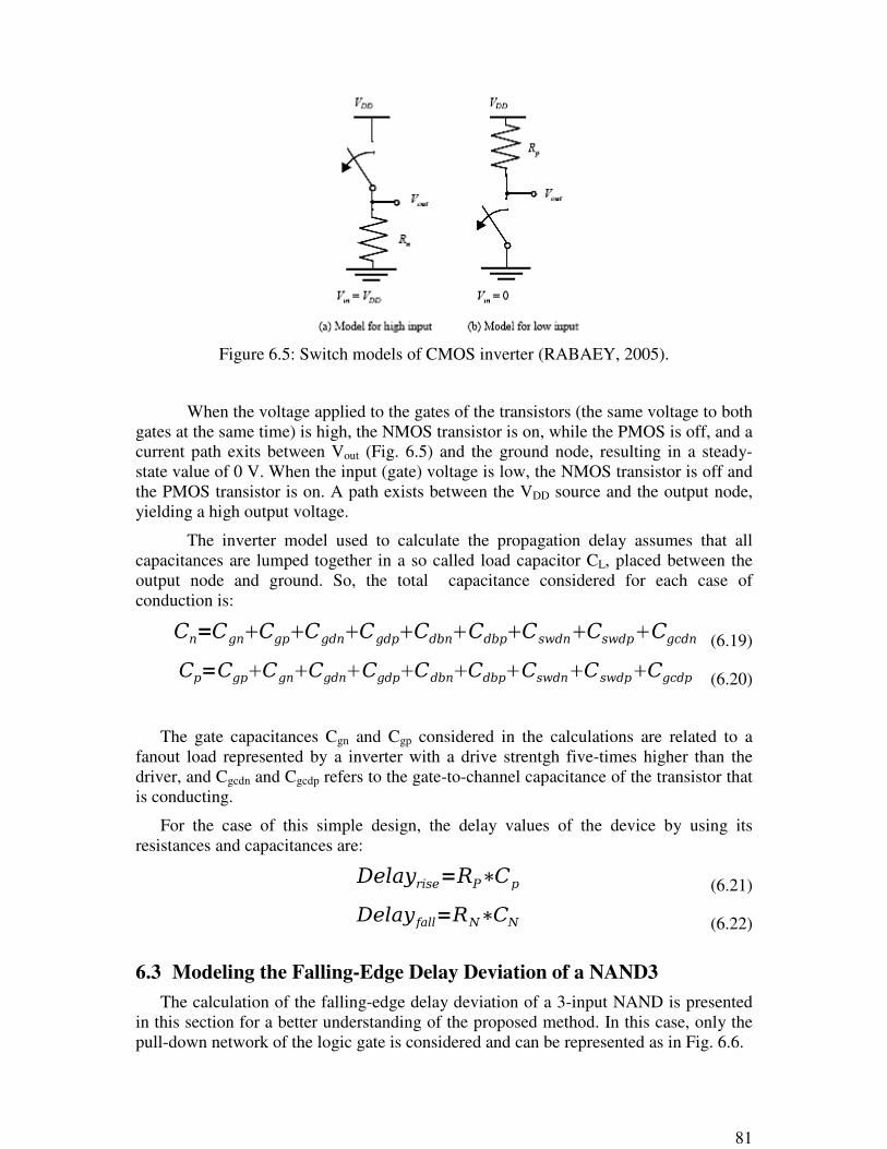
81
Figure 6.5: Switch models of CMOS inverter (RABAEY, 2005).
When the voltage applied to the gates of the transistors (the same voltage to bothgates at the same time) is high, the NMOS transistor is on, while the PMOS is off, and acurrent path exits between Vout (Fig. 6.5) and the ground node, resulting in a steady-state value of 0 V. When the input (gate) voltage is low, the NMOS transistor is off andthe PMOS transistor is on. A path exists between the VDD source and the output node,yielding a high output voltage.
The inverter model used to calculate the propagation delay assumes that allcapacitances are lumped together in a so called load capacitor CL, placed between theoutput node and ground. So, the total capacitance considered for each case ofconduction is:
Cn Cgn Cgp Cgdn Cgdp Cdbn Cdbp Cswdn Cswdp Cgcdn (6.19)
Cp Cgp Cgn Cgdn Cgdp Cdbn Cdbp Cswdn Cswdp Cgcdp (6.20)
The gate capacitances Cgn and Cgp considered in the calculations are related to afanout load represented by a inverter with a drive strentgh five-times higher than thedriver, and Cgcdn and Cgcdp refers to the gate-to-channel capacitance of the transistor thatis conducting.
For the case of this simple design, the delay values of the device by using itsresistances and capacitances are:
Delayrise RP Cp (6.21)
Delay fall RN CN (6.22)
6.3 Modeling the Falling-Edge Delay Deviation of a NAND3The calculation of the falling-edge delay deviation of a 3-input NAND is presented
in this section for a better understanding of the proposed method. In this case, only thepull-down network of the logic gate is considered and can be represented as in Fig. 6.6.
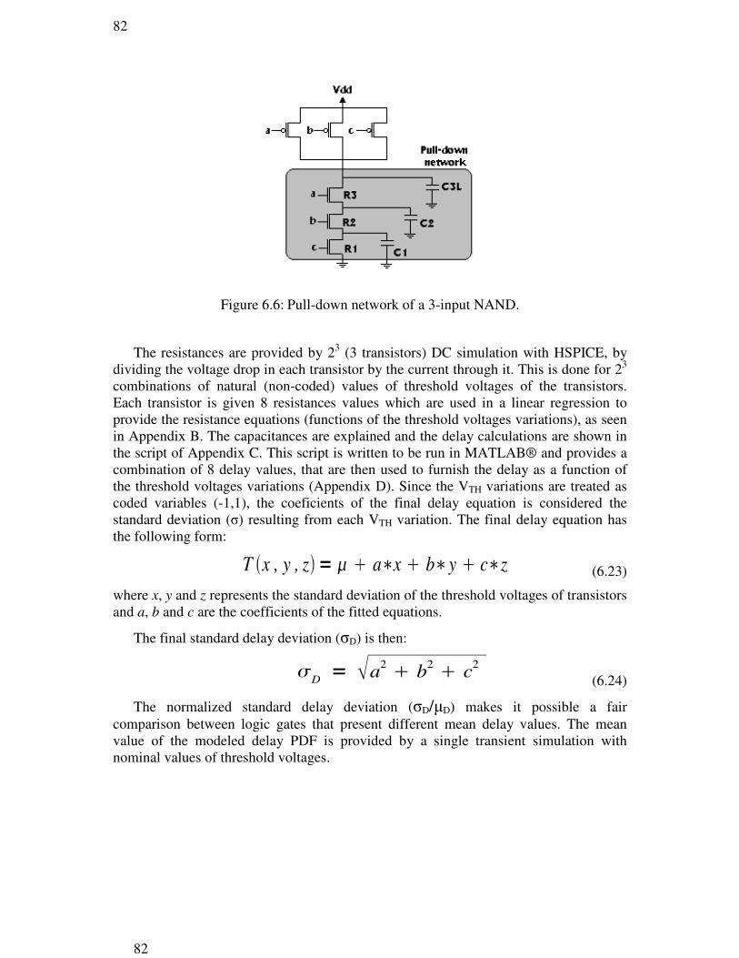
82
82
Figure 6.6: Pull-down network of a 3-input NAND.
The resistances are provided by 23 (3 transistors) DC simulation with HSPICE, bydividing the voltage drop in each transistor by the current through it. This is done for 23
combinations of natural (non-coded) values of threshold voltages of the transistors.Each transistor is given 8 resistances values which are used in a linear regression toprovide the resistance equations (functions of the threshold voltages variations), as seenin Appendix B. The capacitances are explained and the delay calculations are shown inthe script of Appendix C. This script is written to be run in MATLAB® and provides acombination of 8 delay values, that are then used to furnish the delay as a function ofthe threshold voltages variations (Appendix D). Since the VTH variations are treated ascoded variables (-1,1), the coeficients of the final delay equation is considered thestandard deviation (σ) resulting from each VTH variation. The final delay equation hasthe following form:
T x , y , z a x b y c z (6.23)
where x, y and z represents the standard deviation of the threshold voltages of transistorsand a, b and c are the coefficients of the fitted equations.
The final standard delay deviation (σD) is then:
Da
2b
2c
2
(6.24)
The normalized standard delay deviation (σD/µD) makes it possible a faircomparison between logic gates that present different mean delay values. The meanvalue of the modeled delay PDF is provided by a single transient simulation withnominal values of threshold voltages.

83
7 MODELING THE DELAY VARIABILITY OFTRANSISTOR NETWORKS
This chapter presents the results achieved by using the proposed semi-empiricalmethod to calculate the delay deviation of different transistors networks. DC electricalsimulations were performed with HSPICE. The other calculations were performed withthe MATLAB® (Matrix Laboratory) program.
7.1 Calculation of ResistancesIn CHAPTER 6 it has been already explained how the resistances of transistors were
calculated. This section presents an analysis that is able to justify why each transistor ina network must be modeled with different PDFs for its resistances, unless the network ispurely parallel. Fig. 7.1 shows a NMOS stacking and Fig. 7.2 presents the PDFs foreach transistor in the series arrangement.
Figure 7.1: NMOS transistors stacking.
It is quite clear that each transistor has a different resistance mean value andstandard deviation. The variability presented by the resistance of the device that is closeto the output node (far from the ground source) is much higher than the variability ofthose which are respectively closer to the ground source. In this sense, the modeling ofone single transistor as a resistance and the use of this model for the other transistors inthe network implies in a source of error for the delay deviation calculus.

84
84
3000 4000 5000 6000 7000 8000 9000 10000 11000
0,0
0,2
0,4
0,6
0,8
1,0
Norm
aliz
ed P
robabili
ty
Resistance (ohms)
R1 R2 R3 R4
Figure 7.2: Probability density functions (PDF) of the resistances that constitute modelsfor the transistors in a NMOS series network.
7.2 Resistance of Parallel TransistorsThe transistors in a parallel network present equal independent terms and equal
coeficients in the resistance equations, since they are submited to the same drain-sourceand gate-source voltages. Table 7.1 presents resistance equations for N- and PMOSparallel transistors with channel width equals to 90nm. Variables x1, x2, x3 and x4
represent the threshold voltage variations of the respective transistors and are codedwith values of –1 or +1.
Table 7.1: Approximate resistance equations for transistors in a parallel network.
Approximate Resistance EquationsNumber of Transistors
NMOS PMOS
R1 = 6568.5 + 672.4 x1 R1 = 24222 + 1882 x1
R2 = 6568.5 + 672.4 x2 R2 = 24222 + 1882 x2
R3 = 6568.5 + 672.4 x3 R3 = 24222 + 1882 x3
04
R4 = 6568.5 + 672.4 x4 R4 = 24222 + 1882 x4
The resistance (R) of a transistor is not dependent on threshold voltages of othertransistors in the parallel network and the equations are the same for topologies with
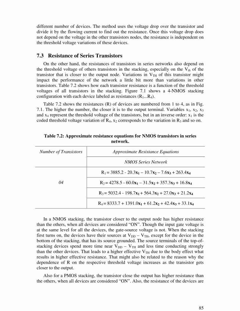
85
different number of devices. The method uses the voltage drop over the transistor anddivide it by the flowing current to find out the resistance. Once this voltage drop doesnot depend on the voltage in the other transistors nodes, the resistance is independent onthe threshold voltage variations of these devices.
7.3 Resistance of Series TransistorsOn the other hand, the resistances of transistors in series networks also depend on
the threshold voltage of others transistors in the stacking, especially on the Vth of thetransistor that is closer to the output node. Variations in VTH of this transistor mightimpact the performance of the network a little bit more than variations in othertransistors. Table 7.2 shows how each transistor resistance is a function of the thresholdvoltages of all transistors in the stacking. Figure 7.1 shows a 4-NMOS stackingconfiguration with each device labeled as resistances (R1...R4).
Table 7.2 shows the resistances (R) of devices are numbered from 1 to 4, as in Fig.7.1. The higher the number, the closer it is to the output terminal. Variables x1, x2, x3
and x4 represent the threshold voltage of the transistors, but in an inverse order: x1 is thecoded threshold voltage variation of R4, x2 corresponds to the variation in R3 and so on.
Table 7.2: Approximate resistance equations for NMOS transistors in seriesnetwork.
Approximate Resistance EquationsNumber of Transistors
NMOS Series Network
R1 = 3885.2 - 20.3x1 – 10.7x2 – 7.6x3 + 263.4x4
R2 = 4278.5 - 60.0x1 – 31.5x2 + 357.3x3 + 16.8x4
R3 = 5032.4 - 198.7x1 + 564.3x2 + 27.0x3 + 21.2x4
04
R4 = 8333.7 + 1391.0x1 + 61.2x2 + 42.4x3 + 33.1x4
In a NMOS stacking, the transistor closer to the output node has higher resistancethan the others, when all devices are considered “ON”. Though the input gate voltage isat the same level for all the devices, the gate-source voltage is not. When the stackingfirst turns on, the devices have their sources at VDD – VTH, except for the device in thebottom of the stacking, that has its source grounded. The source terminals of the top-of-stacking devices spend more time near VDD – VTH and less time conducting stronglythan the other devices. That leads to a higher effective VTH due to the body effect whatresults in higher effective resistance. That might also be related to the reason why thedependence of R on the respective threshold voltage increases as the transistor getscloser to the output.
Also for a PMOS stacking, the transistor close the output has higher resistance thanthe others, when all devices are considered “ON”. Also, the resistance of the devices are

86
86
very dependent on the threshold voltage of the transistor that is far from the output nodeas in Table 7.3.
Figure 7.3: PMOS transistors stacking.
Variable x1 is the coded threshold voltage variation of R4, x2 corresponds to thevariation in R3 and so on.
Table 7.3: Approximate resistance equations for PMOS transistors in seriesnetwork.
Approximate Resistance EquationsNumber of Transistors
PMOS Series Network
R1 = 28434.75 + 40.75x1 + 45x2 + 50.875x3 + 2701.75x4
R2 = 24132 + 75.75x1 + 83.5x2 + 2069x3 - 212.875x4
R3 = 21537.625 + 85.5x1 + 1687.25x2 - 75.125x3 - 88.625x4
04
R4 = 19748.125 + 1431.125x1 - 19.875x2 - 22.5x3 - 26.375x4
Although PMOS transistors can strongly pass “1”, the source of devices far from theVDD source spend more time in a voltage that has an absolute value lower than VDD,since transistors are not ideal switches and present some voltage drop due to theirresistances. Due to the lower absolute gate-source voltage, these devices spend less timeconducting strongly than the other devices, what results in higher effective resistance.
7.4 Estimation of Performance DeviationElmore Delay model (ELMORE, 1948) and Asymptotic Waveform Evaluation
(AWE) (SAPATNEKAR, 2004) were used in the proposed model to calculate the delayvariation for the transistors networks. The threshold voltages of the transistors thatappear in the resistances equations (x1, x2, x3 and x4) were considered as randomvariables represented by probability density functions (PDF) with mean values equal tozero and normalized standard deviations [N(0,1)].
87
7.4.1 Series Networks
The use of Elmore Delay model (ELMORE, 1948) allows us to perform astraightfoward sum operation of PDFs in order to calculate the equivalent resistances ofthe transistors networks, and then the time constant RC. The Asymptotic WaveformEvaluation method requires some other steps before providing a final delay PDF. Asexplained in SECTION 3.5.4, AWE requires the calculations of the conductance andcapacitances matrices by using the equations of the considered circuit. Then themoments are found and matched via Padé approximation resulting in reduced-orderfunction models. In both methods, it is necessary to calculate the delay for the cornervalues of x1, x2, x3 and x4, and fit an equation.
The equations obtained by the estimation method, as those in Table 7.2 and 7.3, areused to perform the analysis described. The procedure is applied only for the resistancesof transistors, since no variations are considered for the capacitances in this work. Theresult is a PDF that represents the delay of the network with the two momentsconsidered: mean and standard deviation (square root of variance). The normalizedstandard deviation (standard deviation divided by the mean) of the delay is the object ofanalysis of different networks, because it makes possible to compare the variability ofarrangements with different mean delays.
Table 7.4 presents the normalized delay deviation for NMOS transistors stackingswith 2, 3 and 4 devices (stack-02, stack-03 and stack-04 respectively), according to theposition of the switching transistor in relation to the output node. Position 1 is theclosest to the output terminal and position 4 is the farthest one.
Table 7.4: Delay deviation for NMOS transistors in series network, according tothe position of the switching transistor in relation to the output node (1-close...4-
far).
Stack-02 Stack-03 Stack-04
Po
siti
on
of
Sw
itch
ing
Tra
nsi
sto
r
Model
Elmore
Model
(AWE)
Simula
tion
Model
Elmore
Model
(AWE)
Simula
tion
Model
Elmore
Model
(AWE)
Simulat
ion
1 0.0520 0.0224 0.0472 0.0472 0.0258 0.0434 0.0438 0.0293 0.0423
2 0.0391 0.0366 0.0451 0.0386 0.0277 0.0381 0.0377 0.0246 0.0346
3 0.0272 0.0318 0.0361 0.0268 0.0273 0.0311
4 0.0217 0.0284 0.0299
The methodology used to find the empirical equations shows that the presence of aswitching transistor in a network causes it to be more sensitive to threshold voltagesvariations. The method proposed by using AWE provides results with an average errorof 25.3%, maximum error equals to 52.5% and minimum error of 5.0% when comparedto the simulated values. It can predict better delay deviations for transitions in devicesfar from the output than for transitions in devices close to output. The number oftransistors in the stacking does not influence much the delay deviation of the network,

88
88
but it can be noticed a little reduction in the metric when more transistors are present.That is similar for the modeled and the simulated situation, except for the “closeswitching”.
Though the results furnished by the method are reasonable, they do not present thesame tendency as the Monte Carlo simulations when the position of the switchingdevice changes for the AWE technique. According to the Monte Carlo simulationsperformed, a “close switching ” causes higher delay deviation independently on thenumber of transistors in the stack. The opposite is presented by the estimation method,according to which a “close switching ” causes lower delay deviation independently onthe number of transistors in the stack.
The proposed model by using Elmore Delay technique provides results with anaverage error of 12.4%, maximum error equals to 27.4% and minimum error of 1.3%.Differently from the results provided by the use of the AWE technique, it presents thesame tendency as the Monte Carlo simulations, in which a “close switching ” causeshigher delay deviation independently on the number of transistors in the stack. Inagreement with the Monte Carlo results, as the number of transistors in the stackdecreases, the delay deviation of the network increases.
Table 7.5 presents the normalized delay deviation for PMOS transistors stackingswith 2, 3 and 4 devices (stack-02, stack-03 and stack 04 respectively), according to theposition of the switching transistor in relation to the output node.
Table 7.5: Delay deviation for PMOS transistors in series network, according tothe position of the switching transistor in relation to the output node (1-close...4-
far).
Stack-02 Stack-03 Stack-04
Po
siti
on
of
Sw
itch
ing
Tra
nsi
sto
r
Model
Elmore
Model
(AWE)
Simula
tion
Model
Elmore
Model
(AWE)
Simula
tion
Model
Elmore
Model
(AWE)
Simulat
ion
1 0.0264 0.0210 0.0382 0.0218 0.0216 0.0379 0.0188 0.0210 0.0403
2 0.0238 0.0218 0.0334 0.0197 0.0198 0.0301 0.0172 0.0155 0.0297
3 0.0188 0.0176 0.0281 0.0163 0.0159 0.0261
4 0.0160 0.0173 0.0249
The model proposed by using AWE provides results with an average error of 39.9%,maximum error equals to 47.9% and minimum error of 30.5%. The number oftransistors in the stacking influences the delay deviation of the network a little bit morethan when NMOS are used. It can also be observed a little reduction in the normalizeddeviation when more transistors are present for simulated and modeled results, but stillnot for the case of a “close switching”. According to statistical simulations performed,a “close switching ” causes higher delay deviation independently on the number oftransistors in the stacking. The same situation is presented by the estimation method,

89
according to which a “close switching ” causes higher delay deviation for the cases with3 and 4 transistors in the stacking.
The model proposed by using Elmore Delay technique provides results with anaverage error of 38.3%, maximum error equals to 53.4% and minimum error of 30.9%.The delay deviation is practically constant for a certain number of transistors in thenetwork independently on the position of the switching transistor, but it decreases as thenumber of transistors increases.
7.4.2 Parallel Networks
Table 7.6 presents the normalized delay deviation for NMOS transistors parallelnetworks with 2, 3 and 4 devices (parallel-02, parallel-03 and parallel-04 respectively).The metrics are presented considering 1, 2 or 3 transistors switching and the other(s)turned off. The equivalent resistance of the parallel arrangement is applied to get the RCtime constant.
Table 7.6: Delay deviation for NMOS transistors in parallel networks, according tothe number of switching transistors.
Parallel-02 Parallel -03 Parallel -04Number of
Switching
Transistors Method Simulation Method Simulation Method Simulation
1 0.0560 0.0545 0.0560 0.0519 0.0560 0.0505
2 0.0431 0.0575 0.0431 0.0536 0.0431 0.0503
3 0.0351 0.0619 0.0351 0.0578
Statistical Monte Carlo simulations presented higher delay deviation for a paralleltransistor network then for a series network. The results provided by the proposedmethod also determined so. Transistors that are not conducting have little influence onthe delay deviation of the arrangement and the model actually presents no influence ofthese devices. The method provides results with an average error of 20.4%, maximumerror equals to 39.3% and minimum error of 2.8%.
The higher the number of switching devices, the higher the delay deviation,according to the simulations. However, the model does not handle the impact ofmultiple switchings on delay deviation, since it presents lower delay deviation as thenumber of switching transistors increases.
On the other hand, the model shows that when all the transistors are conducting, thehigher the number of devices in the network, the lower the delay deviation. That comesin agreement with what was observed in the simulations results: for the same number ofswitching transistors, the fewer the number of devices, the higher the deviation.
Table 7.7 presents the normalized delay deviation for PMOS transistors parallelnetworks with 2, 3 and 4 devices (parallel-02, parallel-03 and parallel-04 respectively).

90
90
Table 7.7: Delay deviation for PMOS transistors in parallel networks, according tothe number of switching transistors.
Parallel-02 Parallel -03 Parallel -04Number of
Switching
Transistors Method Simulation Method Simulation Method Simulation
1 0.0361 0.0426 0.0361 0.0429 0.0361 0.0430
2 0.0257 0.0279 0.0257 0.0278 0.0257 0.0276
3 0.0209 0.0218 0.0209 0.0213
In the case of PMOS transistors networks, the model agrees with the simulationresults when it comes to how the number of switching devices impacts the delaydeviation: the higher the number of switching transistors, the lower the delay deviation.Also, it can be said that both results point to no influence of the turned-off devices onthe this metric. The proposed method provides results with an average error of 7.9%,maximum error equals to 15.9% and minimum error of 1.9%.
7.4.3 Delay Variability Modeled by Considering the Saturated Region ofOperation
As discussed in chapter 6, the on-resistance of an MOS transistor depends upon itsoperation point and varies during the switching transient. The results achieved so farwith the model were based in on-resistances calculated in the linear region of operation,once the DC voltage applied to the devices was set to small values, and so the drain-source voltage of the transistors. This section presents the delay deviations calculatedwith on-resistances of transistors operating in the saturation region with the proposal ofevaluating whether a change in the on-resistances compromises the reliability of themodel or not. If so, it is important to determine the best way of calculating theresistances to be applied in the performance analysis.
Table 7.8 presents the normalized delay deviation for NMOS and PMOS transistorsstackings with 4 devices (stack-04), according to the position of the switching transistorin relation to the output node. The results are provided by modeling the on-resistancesin the linear and in the saturation regions.

91
Table 7.8: Delay deviation for N- and PMOS transistors in series networks,according to the position of the switching transistor in relation to the output node
(1-close...4-far) for the linear and the saturation regions of operation.
NMOS PMOS
Linear Region Saturation
Region
Linear Region Saturation
Region
Po
siti
on
of
Sw
itch
ing
Tra
nsi
sto
r
Sim
ula
tio
n
Mo
del
(AW
E)
Mo
del
Elm
ore
Mo
del
(AW
E)
Mo
del
Elm
ore
Sim
ula
tio
n
Mo
del
(AW
E)
Mo
del
Elm
ore
Mo
del
(AW
E)
Mo
del
Elm
ore
1 0.0423 0.0293 0.0438 0.0171 0.0467 0.0403 0.0210 0.0188 0.0155 0.0141
2 0.0346 0.0246 0.0377 0.0261 0.0451 0.0297 0.0155 0.0172 0.0124 0.0123
3 0.0311 0.0273 0.0268 0.0295 0.0312 0.0261 0.0159 0.0163 0.0128 0.0116
4 0.0299 0.0284 0.0217 0.0278 0.0250 0.0249 0.0173 0.0160 0.0133 0.0113
The bold-faced values represent the best results achieved for the delay deviation byusing AWE or Elmore Delay technique for each type of transistors (N- or PMOS). By“best results” one understand those between the methods using two techniques whichget closer to the results provided by simulations. In the case of a NMOS stacking, themethod applied by using resistances calculated in the linear region of the transistoroperation provides results that are mostly closer to the simulated values. In the case of aPMOS stacking, the estimated results are better when the resistances are extracted in thelinear region for all the positions considered for the switching device. In order to get amore reliable conclusion on which region of operation should be used the calculus ofthe resistances, it is interesting to investigate the delay deviation of another type oftransistor network in relation to the region of operation used to calculate the on-resistances.
Table 7.9 presents the normalized delay deviation for N- and PMOS paralleltransistors networks with 4 devices (Parallel-04), according to the amount of switchingtransistors. The results are provided by modeling the on-resistances in the linear and inthe saturation regions.

92
92
Table 7.9: Delay deviation for N- and PMOS transistors in parallel networks,according to the number of switching transistor for the linear and the saturation
region of operation.
NMOS PMOS
Method MethodPosition of
Switching
Transistor SimulationLinear
Region
Saturation
Region
SimulationLinear
Region
Saturation
Region
1 0.0505 0.0560 0.0605 0.0430 0.0414 0.0251
2 0.0503 0.0431* 0.0435 0.0276 0.0257 0.0178
3 0.0578 0.0351* 0.0354 0.0213 0.0209 0.0146
The results achieved by using the resistances calculated with points in the saturationregion are worse than those achieved with points in the linear region. Actually, thisregion present much worst results for the PMOS transistors networks. By analyzing thedelay deviation values provided, it was found a better choice to stick to the linear regionin order to calculate the on-resistances of the transistors.
7.4.4 Estimation Method Applied to Different Inverter Topologies
As already discussed, a semi-empirical method was developed in order to analyzedelay variability of different transistor networks. This method was applied to theinverter topologies showed in Fig. 5.13 and the results are presented in Table 7.10. Thetotal area for the N- or PMOS network is kept constant for the configurations presented(WN Total = 180nm and WP Total = 680 nm) and the fanout (output load) consists of aninverter with WN = 225nm and WP = 850 nm.
Table 7.10: Rise and fall delay deviations for different inverter topologies.
Timing
Rise Delay Deviation Fall Delay DeviationInverter
Topology
Simulation Method Simulation Method
(a) 0.0415 0.0359 0.0852 0.0595
(b) 0.0319 0.0260 0.0956 0.0448
(c) 0.0283 0.0255 0.0355 0.0522
The method presented delay variability values in agreement to the simulated resultswhen it concerns to the the topology less affected by VTH variations for the rising-edge

93
delay. The falling-edge delay deviation achieved with the method implies in lessvariability for the series topology, while the simulated results points at the folded(parallel) topology as the most immune to variations in VTH. By considering bothdelays, the method establishes the series configuration for the inverter as the mostrobust, while the simulation shows that the folded topology is the best choice.
However, the measurements and calculations that provided the results in Table 7.10do not take into account that, according to Pelgrom model, the larger the size of thetransistor, the lower its threshold voltage deviation. The same deviation (3σ = 10%) wasapplied to the three sizes of inverters analyzed. In order to investigate the influence ofthe area on the standard deviation of VTH and consequently on the delay of the logicgate, different variations were considered for different sizes by applying the relationbetween the parameter variation and the area:
2P
1W.L
as already demonstrated by equation (3.17).
Table 7.11 shows delay deviation results for the same inverter topologies presentedin Table 7.10), but with different VTH standard deviations. The inverter named (a) wasgiven a deviation as before (3σ = 10%). The inverter named (b) was given a deviationof 3σ = 7.07% and the inverter (c) a deviation of 3σ = 14.1% with the fanout consistsof an inverter with WN = 225nm and WP = 450 nm.
.
Table 7.11: Rise and fall delay deviations for different inverter topologies withdifferent threshold voltage variations.
Timing
Rise Delay Deviation Fall Delay DeviationInverter
Topology
Method Simulation Method Simulation
(a) 0.0359 0.0445 0.0595 0.0941
(b) 0.0201 0.0223 0.0321 0.0656
(c) 0.0363 0.0431 0.0618 0.0834
7.4.5 The Influence of the Sizing of Transistors on Delay Variability
The second section of CHAPTER 5 has already discussed the influence of thedimensions of the transistors on the delay variability of an inverter. Table 7.12 showsthe results provided by the proposed method for different drive strengths while keepinga constant ratio of widths (WP/WN). The transistors widths used for the inverters were:(1) WN=0.045µ and WP=0.170µ, (2) WN=0.090µ and WP=0.340µ and (3) WN=0.180µand WP=0.680µ. The threshold voltage variation range is the same for all themeasurements (3σ = 10% variation).

94
94
Table 7.12: Rise and fall delay deviations for different sizes of inverters.
Rise Delay Deviation Fall Delay Deviation
Inverter SizesMethod
(Elmore)
Simulation Method
(Elmore)
Simulation
(1) 0.0360 0.0407 0.0350 0.0415
(2) 0.0359 0.0372 0.0600 0.0556
(3) 0.0359 0.0415 0.0595 0.0852
The results provided by the simulations furnished similar rise delay deviations fordifferently sized inverters. This is also so for the method, which presented near equalresults for the three sizes analyzed. The simulated and modeled results showed anincrease in the fall delay deviation as the sizes of devices increases. The variability inthe performance of the logic gate is more sensitive to the resizing of the NMOS than ofthe PMOS transistor.
Table 7.13 shows delay deviation results for the differently sized devices (the sameas is Table 7.12), but with different VTH standard deviation, as predict by Pelgrommodel. The inverter named (1) was given a deviation as before (3σ = 10%). The inverternamed (2) was given a deviation of 3σ = 7.07% and the inverter (3) a deviation of 3σ =5%.
Table 7.13: Rise and fall delay deviations for different sizes of inverters withdifferent threshold voltage variations.
Rise Delay Deviation Fall Delay Deviation
Inverter SizesMethod
(Elmore)
Simulation Method
(Elmore)
Simulation
(1) 0.0360 0.0407 0.0350 0.0415
(2) 0.0254 0.0271 0.0425 0.0427
(3) 0.0180 0.0223 0.0298 0.0468
The method predicts lower delay variability as the size of the inverter increases andit is in accordance with the model when the rising-edge delay deviation is considered.However, the statistical simulations present higher falling-edge delay deviation whenlarger devices are used. It is the same tendency as showed in Table 7.12, though theincrease in the delay deviation is not so pronounced when the VTH deviation is lowered.The method does not agree with that, once it presents lower falling-edge delay deviationwhen larger devices are used.

95
7.4.6 The Influence of the Output Load on Delay Variability
7.4.6.1 The Series Transistors Networks
In the case of the evaluated N- and PMOS 4- transistor stacking, the method canhandle different fanouts when the Elmore Delay technique is applied, but not if theAWE method is used. In the former, the rising-edge delay deviation decreases when theoutput load driven by the network increases, in accordance with the Monte Carlosimulations. In the later, the delay deviation increases as the fanout increases. Fig. 7.4and 7.5 present the relation between different fanouts and rise delay variability for thestacking transistors analyzed.
Fig. 7.6 and 7.7 present the relation between different fanouts and fall delayvariability for the stacking transistors analyzed. The simulated results for falling-edgedelay variability are not as easily able to fit as the former results. Fig. 7.6 reveals thetendency of a decreased variability for a certain interval in which the output loadincreases, but is is not so for all the fanouts studied. The use of the AWE method fordifferent output loads is the closest tendency one could get to the simulated valuestendency, as shown in Fig. 7.7.
0 2 4 6 8 10 12 14 16 18 20 22
0,028
0,030
0,032
0,034
0,036
0,038
0,040
0,042
Equation: y = A1*exp(-x/t1) + y0 y0 0.02809 ±0.00065A1 0.01771 ±0.00094t1 6.32694 ±0.93147
Norm
aliz
ed R
ise D
ela
y D
evia
tion
Relative Fanout
Statistical Simulation
Fitted Curve
Figure 7.4: Simulated and fitted curves for rising-edge delay deviation in relation to theoutput load of a 4-stacking PMOS network.

96
96
0 2 4 6 8 10 12 14 16 18 20 22
0.0154
0.0156
0.0158
0.0160
0.0162
0.0164
0.0166
0.0168
0.0170
No
rma
lized
Ris
e D
ela
y D
evia
tio
n
Relative Fanout
Equation: y = A1*exp(-x/t1) + y0
y0 0.01542 ±0.00002A1 0.00245 ±0.00008t1 3.53198 ±0.16768
Elmore Delay Deviation
Fitted Curve
Figure 7.5: Modeled and fitted curves for rising-edge delay deviation in relation to theoutput load of a 4-stacking PMOS network using Elmore Delay model.
0 2 4 6 8 10 12 14 16 18 20 220,034
0,036
0,038
0,040
0,042
0,044
0,046
No
rmaliz
ed F
all
Dela
y D
evia
tio
n
Relative Fanout
Statistical Simulation
Figure 7.6: Simulated points for falling-edge delay deviation in relation to the outputload of a 4-stacking NMOS network.

97
0 2 4 6 8 10 12 14 16 18 20 220,024
0,026
0,028
0,030
0,032
0,034
0,036
Equation: y = A1*exp(-x/t1) + y0
y0 0.0257 ±0.00012
A1 0.0155 ±0.00067
t1 3.55241 ±0.21617
AWE Method
Fitted Curve
Norm
aliz
ed F
all
De
lay D
evia
tio
n
Relative Fanout
Figure 7.7: Modeled and fitted curves for falling-edge delay deviation in relation tothe output load of a 4-stacking NMOS network using AWE.
7.4.7 Inverter Chains
The delay deviations of chains with different number of inverters are measured andthe results can be seen in Table 7.14. It is shown in Fig. 7.8 two of the measurementstructures used in this section. In each one, the first two inverters were placed betweenthe ideal voltage source and the gate under analysis (X) in order to provide a morerealistic input slope. From one to five inverters X were placed in the chain and timingdeviations were taken. It also presents results provided by the proposed model. Thedimensions are the same as used before for the case of analyzing inverters: WN =0.045µ and WP=0.170 µ.
Figure 7.8: Measurement structures.

98
98
Table 7.14. Rise and fall delay deviations for different chains of inverters.
Rise Delay Deviation Fall Delay DeviationNumber of
InvertersMethod Simulation Method Simulation
1 0.0360 0.0407 0.0350 0.0415
2 0.0252 0.0293 0.0252 0.0332
3 0.0206 0.0266 0.0205 0.0279
4 0.0178 0.0224 0.0178 0.0253
5 0.0160 0.0209 0.0159 0.0222
In both cases - simulated and modeled – chains with the same numbers of inverterspresent similar rise and fall delay deviations. The results provided by the Monte-Carlosimulations and the semi-empirical method agree in an important point: as the numberof inverters in the chain increases, the normalized deviations of rise and fall delaysdecrease. The proposed model provides results with an average error of 18.4%,maximum error equals to 23.4% and minimum error of 11.6% for the rise delaydeviation. The results for the fall delay deviation present an average error of 24.9%,maximum error equals to 29.6% and minimum error equals to 15.7%.
7.5 ConclusionPrevious simulations with series NMOS transistors revealed lower delay deviation
for a switching transistor close to the output node than for a transition in a device farfrom the output node. For a stack with PMOS transistors higher immunity to variation isachieved when the switching transistor is far from the output terminal. The semi-empirical method achieved for the resistances and used to calculate timing deviation inthe networks has also proved the same tendency for the PMOS network but that was notexactly so for the NMOS network.
The results revealed that, in general, the position of switching transistor impactsmore strongly N- and PMOS stacks with fewer transistors. The model proposed for theresistances of transistors in a network allows one to investigate how variations inthreshold voltage of each device influence the resistance of all devices in thearrangement. By using the resistance functions it is also possible to analyze theperformance variability according to the state and position of the devices in thenetwork. Though Elmore delay technique present some limitations, it is plausible to beused to perform the analysis.
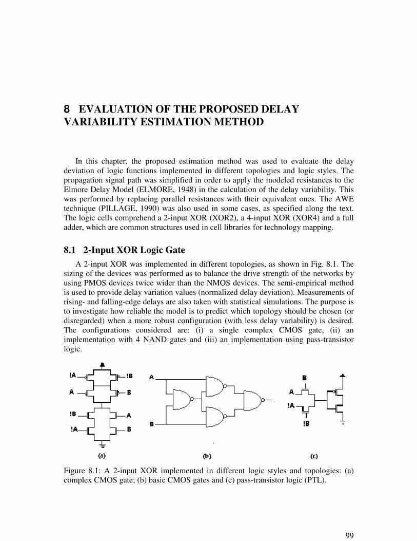
99
8 EVALUATION OF THE PROPOSED DELAYVARIABILITY ESTIMATION METHOD
In this chapter, the proposed estimation method was used to evaluate the delaydeviation of logic functions implemented in different topologies and logic styles. Thepropagation signal path was simplified in order to apply the modeled resistances to theElmore Delay Model (ELMORE, 1948) in the calculation of the delay variability. Thiswas performed by replacing parallel resistances with their equivalent ones. The AWEtechnique (PILLAGE, 1990) was also used in some cases, as specified along the text.The logic cells comprehend a 2-input XOR (XOR2), a 4-input XOR (XOR4) and a fulladder, which are common structures used in cell libraries for technology mapping.
8.1 2-Input XOR Logic GateA 2-input XOR was implemented in different topologies, as shown in Fig. 8.1. The
sizing of the devices was performed as to balance the drive strength of the networks byusing PMOS devices twice wider than the NMOS devices. The semi-empirical methodis used to provide delay variation values (normalized delay deviation). Measurements ofrising- and falling-edge delays are also taken with statistical simulations. The purpose isto investigate how reliable the model is to predict which topology should be chosen (ordisregarded) when a more robust configuration (with less delay variability) is desired.The configurations considered are: (i) a single complex CMOS gate, (ii) animplementation with 4 NAND gates and (iii) an implementation using pass-transistorlogic.
Figure 8.1: A 2-input XOR implemented in different logic styles and topologies: (a)complex CMOS gate; (b) basic CMOS gates and (c) pass-transistor logic (PTL).

100
100
The configurations presented in Fig. 8.1 were modeled in a transistor-level asexplained in CHAPTERS 6 and 7. For each cell, 2k DC simulations for each network(pull-up and pull-down) and one transient simulation for the overall logic gate were runin order to model each gate. Though some results achieved with the model present largeerrors when compared to the simulated ones, they are able to indicate the topology thatis more susceptible to threshold voltage variations among those analyzed for bothrising- and falling-edge delay (Table 8.1).
Table 8.1: Delay deviations for different implementations of a 2-input XORprovided by the proposed method and by statistical simulation.
Rise Delay Deviation Fall Delay DeviationTopology or
Logic Style Method Simulation Error
(%)
Method Simulation Error
(%)
Complex
CMOS Gate0.0258 0.0411 37.2 0.0480 0.0226 112.4
Basic Gates
(NAND)0.0339 0.0287 18.1 0.0306 0.0277 10.1
PTL 0.0252 0.0350 28.0 0.1537 0.1330 15.6
The method was able to predict the large falling-edge delay deviation presented bythe PTL style. It overestimated the falling-edge delay deviation for the complex CMOSgate and the PTL configurations analyzed. Results provided by the proposed methodand the statistical simulations points at the configuration with NAND gates as the mostimmune to variations in VTH when both rising- and falling-edge delay deviations areconsidered.
The highest error presented by the model was for the falling-edge delay deviation ofthe CMOS complex gate by considering the modeled resistances applied to the ElmoreDelay Model. However, the AWE technique was also tested for this case and a betterresult (0.0388) with an error of 71.7 % was achieved.
Complete statistical simulation results are presented in Table 8.2. Regarding themean delay values, the complex gate is the better choice among the configurations.Though it presents the worst rising-edge delay deviation (simulated), it also presents thelower falling-edge delay deviation. The pass-transistor logic revealed itself a bad choiceregarding timing analysis, since it presents the higher overall mean delay and the muchworst overall delay variation.

101
Table 8.2: Delay values and deviations for different implementations of a 2-inputXOR.
Rise Delay Fall DelayTopology or
Logic StyleMean (ps) Absolute
Deviation
(ps)
Normalized
Deviation
Mean (ps) Absolute
Deviation
(ps)
Normalized
Deviation
Complex
CMOS Gate80.003 3.289 0.0411 91.403 2.062 0.0226
Basic Gates
(NAND)190.683 5.464 0.0287 148.191 4.112 0.0277
PTL 90.310 3.163 0.0350 244.602 32.521 0.1330
Once the method presented so far proposes a solution for the delay variability, butnot for its mean value, the analysis was completed by running a single transientsimulation with nominal values of threshold voltages. These nominal delays were thenused, along with the normalized standard deviation provided by the model, to providethe delay probability density functions (normal distributions). Figures 8.2-9 show thedelay PDFs provided by statistical simulations and the PDFs provided by the estimationmethod for each topology. Figures 8.3 and 8.7 show that regarding both rising- andfalling-edge delay, a 2-input XOR implemented with NAND logic gates has its delayPDF very well predict by the proposed method. For the rising-edge delay, the method isoptimistic for the complex gate and the PTL topologies analyzed, once it presentedlower deviation values than those provided by the simulations.

102
102
6,00E-011 7,00E-011 8,00E-011 9,00E-011 1,00E-010
0,0
0,2
0,4
0,6
0,8
1,0
No
rma
lize
d P
rob
ab
ility
Simulation
Method
Rising-Edge Delay
Complex
Gate
Figure 8.2: PDF of the rising-edge delay for the complex gate implementation of a 2-input XOR.
1,60E-010 1,80E-010 2,00E-010 2,20E-010
0,0
0,2
0,4
0,6
0,8
1,0
No
rma
lize
d P
roba
bili
ty
Simulation
Method
Rising-Edge Delay
NAND
Gates
Figure 8.3: PDF of the rising-edge delay for the implementation of a 2-input XOR withNAND gates.

103
7,00E-011 8,00E-011 9,00E-011 1,00E-010 1,10E-010
0,0
0,2
0,4
0,6
0,8
1,0
Norm
aliz
ed P
rob
ab
ility
Simulation
Method
PTL
Rising-Edge Delay
Figure 8.4: PDF of the rising-edge delay for the PTL implementation of a 2-input XOR.
8,00E-011 1,20E-010 1,60E-010 2,00E-010
0,0
0,2
0,4
0,6
0,8
1,0PTLComplex
GateNAND
Gates
Rising-Edge Delay
Norm
aliz
ed P
robabili
ty
Simulation
Method
Figure 8.5: PDF of rising-edge delay for different implementations of a 2-input XOR.
Fig. 8.6 shows that the results provided by the method for the complex gateconfiguration is very pessimistic when falling-edge delay deviation is considered. Themethod was able to predict the large variability presented by the DPTL logic style, what

104
104
may cause the use of this configuration to be prohibitive in certain designs, for the sakeof parametric yield improvement.
7,00E-011 8,00E-011 9,00E-011 1,00E-010 1,10E-010
0,0
0,2
0,4
0,6
0,8
1,0
Simulation
Method
N
orm
aliz
ed P
robabili
ty
Falling-Edge Delay
Complex
Gate
Figure 8.6: PDF of the falling-edge delay for the complex gate implementation of a 2-input XOR.
1,20E-010 1,30E-010 1,40E-010 1,50E-010 1,60E-010 1,70E-010
0,0
0,2
0,4
0,6
0,8
1,0
Norm
aliz
ed P
roba
bili
ty
Falling-Edge Delay
Simulation
Model
NAND
Gates
Figure 8.7: PDF of the falling-edge delay for the implementation of a 2-input XORwith NAND gates.

105
1,00E-010 2,00E-010 3,00E-010 4,00E-010
0,0
0,2
0,4
0,6
0,8
1,0
Norm
aliz
ed P
robab
ility
Simulation
Method
Falling-Edge Delay
PTL
Figure 8.8: PDF of the falling-edge delay for the PTL implementation of a 2-inputXOR.
1,00E-010 2,00E-010 3,00E-010 4,00E-010
0,0
0,2
0,4
0,6
0,8
1,0Complex
GatePTLNAND
Gates
Norm
aliz
ed
Pro
ba
bili
ty
Falling-Edge Delay
Simulation
Method
Figure 8.9: PDF of the falling-edge delay for different implementations of a 2-inputXOR.
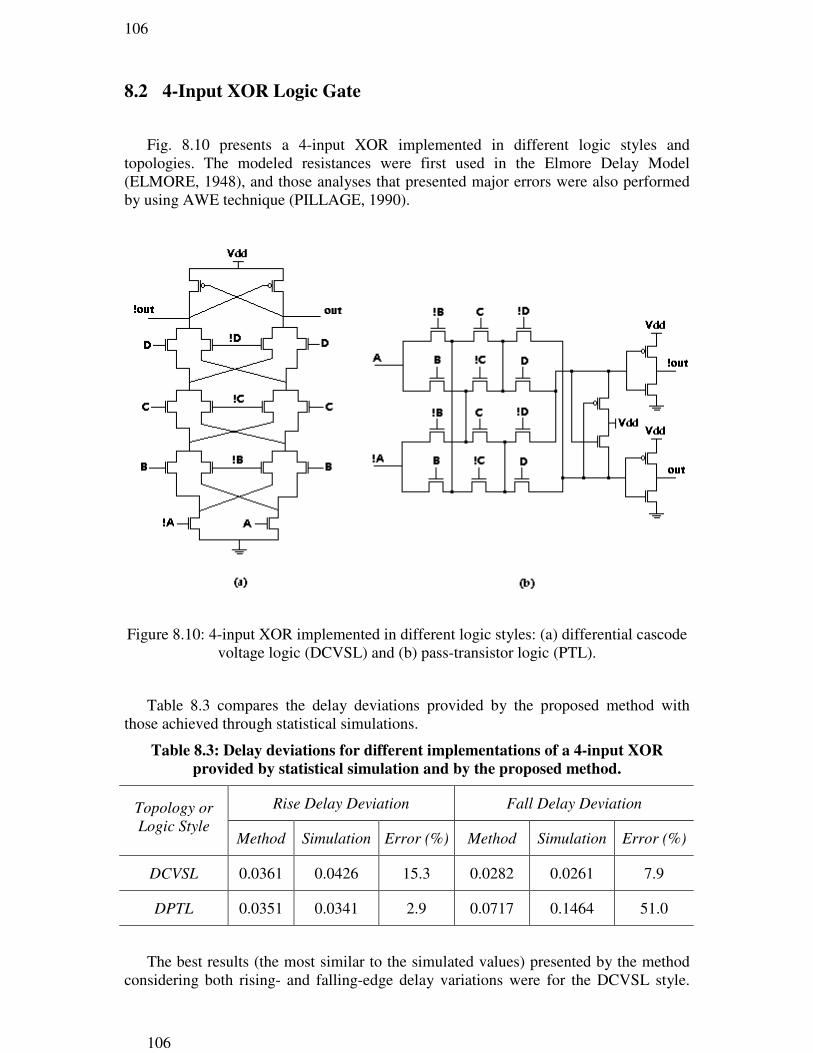
106
106
8.2 4-Input XOR Logic Gate
Fig. 8.10 presents a 4-input XOR implemented in different logic styles andtopologies. The modeled resistances were first used in the Elmore Delay Model(ELMORE, 1948), and those analyses that presented major errors were also performedby using AWE technique (PILLAGE, 1990).
Figure 8.10: 4-input XOR implemented in different logic styles: (a) differential cascodevoltage logic (DCVSL) and (b) pass-transistor logic (PTL).
Table 8.3 compares the delay deviations provided by the proposed method withthose achieved through statistical simulations.
Table 8.3: Delay deviations for different implementations of a 4-input XORprovided by statistical simulation and by the proposed method.
Rise Delay Deviation Fall Delay DeviationTopology or
Logic StyleMethod Simulation Error (%) Method Simulation Error (%)
DCVSL 0.0361 0.0426 15.3 0.0282 0.0261 7.9
DPTL 0.0351 0.0341 2.9 0.0717 0.1464 51.0
The best results (the most similar to the simulated values) presented by the methodconsidering both rising- and falling-edge delay variations were for the DCVSL style.

107
The method was able to predict the least robust configuration among those used toimplement the 4-input XOR gate. The highest error presented by the model was for thefalling-edge delay deviation of the DPTL style by considering the modeled resistancesapplied to the Elmore Delay Model. However, the AWE technique was tested for thiscase and a better result (0.1314), with an error of 10.3 % was achieved.
Rise and fall delay mean values as well as their deviations provided by statisticalsimulations are found in Table 8.4. The complex gate implementation presented goodoverall variability results and the lowest rise delay deviation among the topologiesstudied.
Table 8.4. Delay values and deviations for different implementations of a XOR4.
Rise Delay Fall DelayLogic Style
Mean (ps) Absolute
Deviation
(ps)
Normalized
Deviation
Mean (ps) Absolute
Deviation
(ps)
Normalized
Deviation
DCVSL 341.803 14.554 0.0426 67.737 1.769 0.0261
DPTL 315.539 10.749 0.0341 310.429 45.456 0.1464
Definitely, the pass-transistor logic style was the configuration that presented worstdeviation results, especially for the falling-edge delay, where it also presented the worstmean delay value. However, for the rising-edge delay it was the best topology amongthose presented.
Fig. 8.11 and 8.12 show the probability density functions of rise and fall delays foreach configuration. The method presented a reliable rising-edge delay deviation for thetopologies studied, since it provided PDFs that are very close to the statisticallysimulated ones.

108
108
2,80E-010 3,20E-010 3,60E-010 4,00E-010
0,0
0,2
0,4
0,6
0,8
1,0
Norm
aliz
ed P
robabili
ty
Simulation
Method
Rising-Edge Delay
DCVSL
Figure 8.11: PDF of the rising-edge delay for the DCVSL implementation of a 4-inputXOR.
2,80E-010 3,20E-010 3,60E-010
0,0
0,2
0,4
0,6
0,8
1,0
Norm
aliz
ed P
robabili
ty
DPTL Simulation
Method
Rising-Edge Delay
Figure 8.12: PDF of the rising-edge delay for the DPTL implementation of a 4-inputXOR.

109
2,80E-010 3,20E-010 3,60E-010 4,00E-010
0,0
0,2
0,4
0,6
0,8
1,0
No
rma
lize
d P
roba
bili
ty
Rising-edge Delay
Simulation
Method
DPTL DCVSL
Figure 8.13: PDF of rising-edge delay for different implementations of a 4-input XOR.
In Fig. 8.16 it is remarkable the high falling-edge delay deviation presented by thepass-transistor logic style. The method was very optimistic for the DPTL style,providing lower delay deviation for this topology when Elmore Delay model wasapplied to calculate the deviation. Despite of its limitation regarding the DPTL style, themethod is able to predict the configuration with the highest variability among thoseevaluated. The method presented good reliability for the DCVSL topology.

110
110
5,60E-011 6,00E-011 6,40E-011 6,80E-011 7,20E-011 7,60E-011 8,00E-011
0,0
0,2
0,4
0,6
0,8
1,0
DCVSL
Falling-Edge Delay
No
rma
lize
d P
roba
bili
ty
Simulation
Method
Figure 8.14: PDF of the falling-edge delay for the DCVSL implementation of a 4-inputXOR.
0,00E+000 2,00E-010 4,00E-010 6,00E-010
0,0
0,2
0,4
0,6
0,8
1,0 DPTL
No
rma
lize
d P
rob
abili
ty
Falling-Edge Delay
Simulation
Method
Figure 8.15: PDF of falling-edge delay for the DPTL implementation of a 4-inputXOR.

111
1,00E-010 2,00E-010 3,00E-010 4,00E-010 5,00E-010
0,0
0,2
0,4
0,6
0,8
1,0
Falling-edge Delay
Norm
aliz
ed P
rob
abili
ty
CVSL DPTL Simulation
Method
Figure 8.16: PDF of falling-edge delay for different implementations of a 4-input XOR.
Fig. 8.17 shows the probability density functions of falling-edge delay for the DPTLimplementation by considering the deviation provided by the method when AWEtechnique is used. The modeled PDF is much more similar to the simulated one than inFig. 8.15.

112
112
0,00E+000 2,00E-010 4,00E-010 6,00E-010
0,0
0,2
0,4
0,6
0,8
1,0
Norm
aliz
ed P
robabili
ty
Falling-Edge Delay
Simulation
Method
DPTL
Figure 8.17: PDF of falling-edge delay for DPTL implementation of a 4-input XORmodeled with AWE technique.
8.3 Full AdderThe full adder is a logic cell with three inputs and two outputs (WESTE, 2005) and
it presents the logic functions summarized in the truth table showed in Table 8.5:
Table 8.5. Truth table of a full adder.
Inputs Outputs
CIN B A COUT SUM
0 0 0 0 0
0 0 1 0 1
0 1 0 0 1
0 1 1 1 0
1 0 0 0 1
1 0 1 1 0
1 1 0 1 0
1 1 1 1 1
The relation between the inputs and the “SUM” output can be represented as thefollowing logic functions:
The presence of a carry-in input and a carry-out output makes the full adder highlyscalable and it is found in many cascade circuit implementations. A full adder wasimplemented in two different logic styles: (i) a complex CMOS gate and (ii) in the

113
differential pass-transistor logic (DPTL). The topologies shown in Fig. 8.18 provide the“SUM” output of the logic cell.
Figure 8.18: Full adder implemented in different logic styles and topologies: (a)complex CMOS gate; (b) differential pass-transistor logic (DPTL).
Table 8.6 compares the delay deviations provided by the proposed method withthose achieved through statistical simulations.
Table 8.6: Delay deviations for different implementations of a full adderprovided by statistical simulation and by the proposed method.
Rise Delay Deviation Fall Delay DeviationTopology or
Logic StyleMethod Simulation Error (%) Method Simulation Error (%)
Complex Gate 0.0162 0.0234 30.8 0.0376 0.0314 19.7
DPTL 0.0316 0.0207 52.7 0.1194 0.0867 37.7
The complex gate presented in Fig. 8.7a has the highest rise delay deviation and thelogic cell in Fig. 8.7b has the highest fall delay deviation according to the statisticalsimulations. The NMOS network of the complex CMOS is more susceptible tovariations than the PMOS network, as seen in CHAPTER 7. The method agrees withthe simulation results when it regards the falling-edge delay deviation, showing that theDPTL topology is the least robust.
The error presented by the method for the falling-edge delay deviation of the DPTLstyle by considering the modeled resistances applied to the Elmore Delay Model wasreduced to 17.2 % when the resistances were used in the AWE technique. In this case,

114
114
the deviation was 0.1016. No better result was achieved when AWE was used in themodel to calculate the rising-edge delay deviation of the DPTL style and the errorremained around 50%.
The results of rise and fall delay measurements for the “SUM” output node areshown in Table 8.7.
Table 8.7. “SUM” delay deviation for different implementations of a full adder.
Rise Delay Fall Delay
Topology /
Logic Style Mean (ps)
Absolute
Deviation
(ps)
Normalized
DeviationMean (ps)
Absolute
Deviation
(ps)
Normalized
Deviation
Complex
Gate267.387 6.256 0.0234 81.626 2.560 0.0314
DPTL 293.651 6.077 0.0207 221.442 19.198 0.0867
As can be seen in Fig. 8.9 and 8.10, the method is reliable for the cell in the DPTLstyle if one consider that the worst delay mean value of this logic style is the rising-edgedelay, whose variability was overestimated by the method, providing a safe margin.
The normal distributions of simulated and modeled delay deviations presented thecomplex CMOS gate as the most apropriate topology to be used in this implementation.The method was more precise when it was applied to the CMOS complex gate(especially for the falling-edge delay), but it was also reliable when used for the DPTLstyle, since it was a little bit pessimistic.
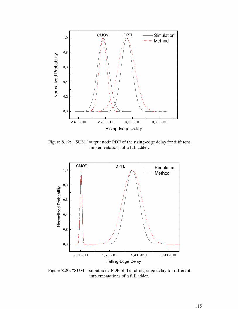
115
2,40E-010 2,70E-010 3,00E-010 3,30E-010
0,0
0,2
0,4
0,6
0,8
1,0
Norm
aliz
ed
Pro
ba
bili
ty
Rising-Edge Delay
Simulation
Method
DPTLCMOS
Figure 8.19: “SUM” output node PDF of the rising-edge delay for differentimplementations of a full adder.
8,00E-011 1,60E-010 2,40E-010 3,20E-010
0,0
0,2
0,4
0,6
0,8
1,0DPTLCMOS
No
rmaliz
ed
Pro
ba
bili
ty
Falling-Edge Delay
Simulation
Method
Figure 8.20: “SUM” output node PDF of the falling-edge delay for differentimplementations of a full adder.

116
116
8.4 Complex GateThe method was also used to evaluate the delay variability of the complex gate
configuration showed in Fig. 8.21.
Figure 8.21: A complex gate implementation;
Table 8.8: Delay deviations for a complex gateprovided by statistical simulation and by the proposed method.
Rise Delay Deviation Fall Delay DeviationTopology or
Logic StyleMethod Simulation Error (%) Method Simulation Error (%)
Complex Gate 0.0190 0.0224 15.2 0.0291 0.0311 6.4
The method was very reliable in the evaluation of both rising- and falling-edge delaydeviations of the complex gate.

117
3,20E-010 3,40E-010 3,60E-010 3,80E-010 4,00E-010
0,0
0,2
0,4
0,6
0,8
1,0
Norm
aliz
ed P
robabili
ty
Rising-Edge Delay
Simulation
Method
Figure 8.22: PDF of the rising-edge delay for the complex gate implementation.
9,00E-011 1,00E-010 1,10E-010 1,20E-010
0,0
0,2
0,4
0,6
0,8
1,0
No
rmaliz
ed
Pro
ba
bili
ty
Falling-Edge Delay
Simulation
Method
Figure 8.23: PDF of the falling-edge delay for the complex gate implementation.
8.5 Delay Equation MethodAs an alternative to the computationally expensive Monte Carlo simulations, the
here so-called Delay Equation Method (DEM) also uses a least square method in order

118
118
to derive the coefficients of the first-order model (delay equation) as a function of thetransistors threshold voltage variations by using SPICE simulations. The difference ofthis method from the estimation method proposed in this work is basically that itrequires transient simulations in spite of the DC type ones. In this sense, DEM does notuse the RC constant of the network in order to provide the delay of the logic cell. Thedelay is the metric directly provided by the transient simulations.
Variations of this method are already available in the literature (OKADA 2003) andthat is why the analysis provided by the proposed estimation method is compared to theDEM in the next sub-section, regarding the runtime. Since this approach can be used toprovide the PDF of a logic cell delay without the need of performing Monte Carlosimulations, it is fair that the proposed method is also compared with DEM.
8.6 Runtime AnalysisThe characterization of the logic gates by using Monte Carlo approach is
computationally expensive and takes a long time to be completed (see Table 8.9 for10.000 runs), what makes it prohibitive in some cases. The approach presented in thiswork to characterize the cells requires simulations that takes only a few seconds, sinceonly one of them is a transient run and all the others are DC. An impressive speedupcan be observed for all the gates analyzed.
The approaches were applied to the 2-input XOR (complex gate topology), to the 4-input XOR (DCVSL logic style) and to the complex gate topology in Fig. 8.21. Table8.9-11 shows the delay (also deviation) results and the runtime analysis of thesestructures for the three methods presented: (i) the proposed estimation method, (ii) thedelay equation method (DEM) and (iii) the statistical simulation (Monte Carlo).
Table 8.9: Delay and runtime analysis for different implementations of a XOR2.
Rise Delay Fall Delay
COMPLEX
GATEMean
Delay
(ps)
Standard
Deviation
(ps)
Normalized
Deviation
Mean
Delay
(ps)
Standard
Deviation
(ps)
Normalized
Deviation
Runtime
Analysis
Estimation
Method79.8 2.1 0.0258 91.3 4.4 0.0480 3s
Delay
Equation
Method
80.0 3.3 0.0409 92.3 2.0 0.0219 37s
Statistical
Simulation
(Monte
Carlo)
80.0 3.3 0.0411 91.4 2.1 0.0226 6.1 h

119
Table 8.10: Delay and runtime analysis of the complex gate topology by usingdifferent methods.
Rise Delay Fall Delay
COMPLEX
GATEMean
Delay
(ps)
Standard
Deviation
(ps)
Normalized
Deviation
Mean
Delay
(ps)
Standard
Deviation
(ps)
Normalized
Deviation
Runtime
Analysis
Estimation
Method359.1 6.8 0.0190 106.9 3.1 0.0291 11s
Delay
Equation
Method
362.5 6.9 0.0191 108.1 2.8 0.02632385s
~ 40min
Statistical
Simulation
(Monte
Carlo)
359.6 8.0 0.0224 107.2 3.3 0.0311 13.7 h
As already seen in SECTION 8.4, the results provided by the estimation methodwere quite close to the statistically simulated ones. Table 8.11 shows the delay and itsdeviation results and the runtime analysis of the 4-input XOR implemented with theDCVSL topology.
Table 8.11: Delay and runtime analysis of the XOR4 implemented with a DCVSLtopology by using different methods.
Rise Delay Fall DelayXOR4
DCVSL
Mean
Delay
(ps)
Standard
Deviation
(ps)
Normalized
Deviation
Mean
Delay
(ps)
Standard
Deviation
(ps)
Normalized
Deviation
Runtime
Analysis
Estimation
Method340.8 12.3 0.0361 67.6 2.0 0.0291 10s
Delay
Equation
Method
342.2 4.4 0.0128 68.3 1.5 0.02181474s
~ 25min
Statistical
Simulation
(Monte
Carlo)
341.8 14.6 0.0426 67.7 1.8 0.0261 16.6 h
Tables 8.10 and 8.11 show that the DEM also presented good results, but at theexpense of a higher simulation runtime than the proposed method.
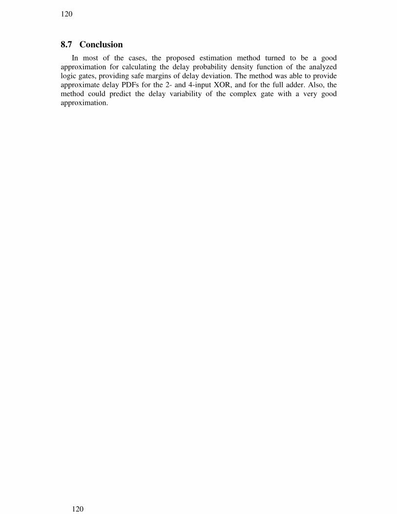
120
120
8.7 ConclusionIn most of the cases, the proposed estimation method turned to be a good
approximation for calculating the delay probability density function of the analyzedlogic gates, providing safe margins of delay deviation. The method was able to provideapproximate delay PDFs for the 2- and 4-input XOR, and for the full adder. Also, themethod could predict the delay variability of the complex gate with a very goodapproximation.

121
9 CONCLUSION
Different topologies of inverters present different delay deviations when thethreshold voltages of transistors vary. Preliminary analysis based on Monte Carlosimulations showed that, for a certain logic function, the choice of the topology and/orlogic style, the number of transistors in the network and the position of a switchingtransistor in relation to the output node influence the delay variability of the logic cell.When only a set of transistors is analyzed, as the pull-up or the pull-down network in aCMOS configuration for example, better results (less delay deviation) were achieved fora higher number of transistors in the arrangement.
The variability estimation method proposed was mainly applied to complementaryMOS (CMOS) logic style, and also presented valuable results for DCVSL, PTL andDPTL styles. For composing the method, the resistance of each transistor wascalculated as a function of the threshold voltages variations of all the devices in thenetwork. Each topology required a 2.2k DC electrical simulations, which took less than10 seconds even for logic gates with more than 10 transistors. The use of two differentregions of operation – linear and saturation – in order to achieve the resistances valuesshowed that the linear region provides more reliable resistance model functions.
The calculus of the resistances was done for each type of transistor (pull-up or pull-down configuration) at a time. In this sense, the on-resistance of NMOS transistors donot depend on the characteristics of PMOS, and vice-versa. This point may be importantto explain the differences between the delay variability provided by NAND and NORgates (CHAPTER 5) and the structures analyzed in CHAPTER 7. In this chapter, theconfigurations were simulated with Monte Carlo by considering only one type ofnetwork (only pull-up or pull-down configurations) and not a complete logic gate.
The analysis of networks with series and parallel transistors revealed considerabledifferences whether N- or PMOS devices compose the arrangement. NMOS networkshave delay deviations that are more sensitive to variations in the threshold voltages oftransistors. In general, a higher number of MOS in a stacking topology represents amore robust arrangement. According to the position of a switching transistor, it is seenthat N- and PMOS transistors switching far from the output node results in lower delaydeviations. In a pure parallel network, variations in the threshold voltages of transistorsthat are not conducting have no influence on delay variability.
In the case of inverters designed with different topologies when the VTH deviation ischanged according to the dimensions of the transistors (Pelgrom model) it is clear thatlarger MOS devices provide lower delay variability.
Results provided by both simulations and modeling also showed that for a chain ofinverters, the higher the number of inverters in the chain, the lower the rising- and
122
122
falling-edge delay deviations. Finally, the comparison of different topologies and logicstyles used to implement the same logic function – a 2-input XOR – showed that thedelay of the configuration with NAND gates suffers less influence of the thresholdvoltage variations of transistors. The pass-transistor logic presented the highest delaydeviation among the topologies analyzed. The logic gate(s) was(were) also analyzedwith the proposed method, which provided compatible results with the statisticalsimulations. In the case of a 4-input XOR, the gate implemented in the DCVSL styleappears as the most reliable configuration among those analyzed. For the full adderlogic cell, the complex CMOS gate is preferible over the DPTL style, when the delay ofthe “SUM” output node is analyzed.
The discrepancies between the simulation results and the delay deviations providedby the estimation method can be partly explained by the limitations of the later. Themethod does not take into account the effect of threshold voltage variations on the gatecapacitances of devices. Also, the logic cell has its rising- and falling-edge delay pathsanalyzed separately, then the model does not regard the influence of devices of the pull-up network on the pull-down network, and vice-versa. Other limitation is the modelingof the devices, once the calculation of the resistances of transistors is only anapproximation of their actual behavior. However, in order to provide the delayprobability density function of a certain topology, the proposed method demands aruntime that is around 3.000x smaller than that demanded by the Monte Carlo method(10.000 runs) . The runtime is also much smaller than that of the so-called DEM.

123
REFERENCES
AMIN, C. et al. A Multi-Port Current Source Model for Multiple-Input SwitchingEffects in CMOS Library Cells. In: DESIGN AUTOMATION CONFERENCE, 43rd,San Francisco, USA. Proceedings... ACM Press, p. 247-252, July 2006.
ARGAWAL, A. et al. Path-Based Statistical Timing Analysis Considering Inter andIntra-Die Correlations. IEEE Transactions on Computer-Aided Design of IntegratedCircuits and Systems, p. 621-625, 2003.
ARGAWAL, K. et al. Parametric Yield Analysis and Optimization in LeakageDominated Technologies. IEEE Transactions on VLSI Systems, New York, USA, v.15, n. 6, p. 613-623, June 2007.
ARUNACHALAM, R., DARTU, F., PILEGGI, L. CMOS Gate Delay Models forGeneral RLC Loading. IEEE International Conference on Computer Design. pp.224-229, October 1997.
BERKELAAR, M. Statistical Delay Calculation, A Linear Method, TAU, p. 15-24,1997.
BLAAUW, D., ZOLOTOV, V., SUNDARESWARAN, S. Slope Propagation in StaticTiming Analysis. IEEE Transactions on Computer-Aided Design of IntegratedCircuits and Systems, v. 21, n. 10, October 2002.
CAO, Y., CLARK, L. T. Mapping Statistical Process Variations Toward CircuitPerformance Variability: An Analytical Modeling Approach. In: DESIGNAUTOMATION CONFERENCE, 42nd, Anaheim, USA. Proceedings... ACM Press, p.13-17, June 2005.
CELIK, M., PILEGGI, L., ODABASIOGLU, A. IC Interconnect Analysis. Springer,2002.
CHIANG, C., KAWA, J. Design for Manufacturability and Yield for Nano-ScaleCMOS. Springer Netherlands, 2007.
CHOI, S., PAUL, B., ROY, K. Novel Sizing Algorithm for Yield Improvement underProcess Variation in Nanometer Technology. In: DESIGN AUTOMATIONCONFERENCE, 41st, San Diego, USA. Proceedings... ACM Press, p. 454-459, June2004.

124
124
CROIX, J., WONG, D. Blade and Razor: Cell and Interconnect Delay Analysis UsingCurrent-Based Models. In: DESIGN AUTOMATION CONFERENCE, 40th, Anaheim,USA. Proceedings... ACM Press, p. 386-389, June 2003.
DAGA, J., AUVERGNE, D. A Comprehensive Delay Macro Modeling forSubmicrometer CMOS Logics. IEEE Journal of Solid-State Circuits, v. 34, n. 1,January 1999.
DARTU, F., MENEZES, N., PILEGGI, L. Performance Computation forPrecharacterized CMOS Gates with RC Loads. IEEE Transactions on Computer-Aided Design of Integrated Circuits and Systems, v. 15, n. 5, May 1996.
DARTU, F., PILEGGI, L. Calculating Worst-Case Gate Delays due to DominantCapacitance Coupling. In: DESIGN AUTOMATION CONFERENCE, 34th, Anaheim,USA. Proceedings... ACM Press, p. 46-51, June 1997.
ELMORE, W. C. The Transient Analysis of Damped Linear Networks with ParticularRegard to Wideband Amplifiers. J. Applied Physics, v. 19, n. 1, p. 55-63, 1948.
FATEMI, H., NAZARIAN, S., PEDRAM, M. Statistical Logic Cell Delay AnalysisUsing a Current-based Model. In: DESIGN AUTOMATION CONFERENCE, 43rd, SanFrancisco, USA. Proceedings... ACM Press, p. 253-256, July 2006.
GUPTA, R., TUTUIANU, B., PILEGGI, L. The Elmore Delay as a Bound for RC Treeswith Generalized Input Signals. IEEE Transactions on Computer-Aided Design ofIntegrated Circuits and Systems, v. 16, n. 1, p. 95-104, January 1997.
HOON CHOI, S., PAUL, B., ROY, K. Novel Sizing Algorithm for Yield Improvementunder Process Variation in Nanometer Technology. In: DESIGN AUTOMATIONCONFERENCE, 41st, San Diego, USA. Proceedings... ACM Press, p. 454-459, June2004.
JAEGER, R. Introduction to Microelectronic Fabrication. Upper Saddle River:Prentice Hall, 2002.
JESS, J., KALAFALA, K., NAIDU, S., OTTEN, R., VISWESWARIAH, C. StatisticalTiming for Parametric Yield Prediction of Digital Integrated Circuits. IEEETransactions on Computer-Aided Design of Integrated Circuits and Systems, v. 25,n. 11, November 2006.
JIANG, Y., SAPATNEKAR, S., BAMJI, C., KIM, J. Combined Transistor Sizing withBuffer Insertion for Timing Optimization. In: CUSTOM INTEGRATED CIRCUITSCONFERENCE, Santa Clara, USA. Proceedings... IEEE, p. 605-608, 1998.
KOUNO, T., HASHIMOTO, M., ONODERA, H. Input Capacitance Modeling of LogicGates for Accurate Static Timing Analysis. Asian Solid-State Circuits Conference, p.453-456, November 2005.
KORSHAK, A., LEE, J. An Effective Current Source Cell Model for VDSM DelayCalculation, 2001 International Symposium on Quality Electronic Design, p.296-300, 2001.
125
MAHMOODI H., MUKHOPADHYAY S., ROY K. Estimation of delay variations dueto random-dopant fluctuations in nanoscale CMOS circuits. IEEE Journal of Solid-State Circuits, v. 40, p. 1787-1796, September 2005.
MAURINE et al. Transition Time Modeling in Deep Submicron CMOS. IEEETransactions on Computer-Aided Design of Integrated Circuits and Systems. v. 21,p. 1352-1363, November 2001.
MYERS, R. H., MONTGOMERY, D. C. Response Surface Methodology: Process andProduct Optimization Using Designed Experiments. 2 Ed. John Wiley & Sons, Inc,2002.
MODE, E. Elements of Probability and Statistics. Englewood Cliffs: Prentice-Hall,c1966.
NASSIF, S. Design for Variability in DSM Technologies. IEEE 2000 FirstInternational Symposium on Quality Electronic Design, p. 451-454, March 2000.
OKADA, K., YAMAOKA, K., ONODERA, H. Statistical Modeling of Gate DelayVariation with Consideration of Intra-Gate Variability. IEEE Transactions onComputer-Aided Design, v. 5, p. 513-516, May 2003.
OLIVIERI M., SCOTTI G., TRIFILETTI A. A novel yield optimization technique fordigital CMOS circuits design by means of process parameters run-time estimation andbody bias active control. IEEE Transactions Very Large Scale Integration (VLSI)Systems, v. 13, p. 630-638, May 2005.
ORSHANSKY, M., NASSIF, S., BONING, D. Design for Manufacturability andStatistical Design: A Constructive Approach. Springer, 2008.
PAN, M., CHU, C., ZHOU, H. Timing Yield Estimation Using Statistical Static TimingAnalysis. IEEE International Symposium on Circuits and Systems, v. 3, p. 2461-2464, May 2005.
PELGROM, M., DUINMAIJER, A., WELBERS, A. Matching Properties of MOSTransistors. IEEE Journal of Solid-State Circuits, v. 24, n.5, October 1989.
PILEGGI, L. Timing Metrics for Physical Design of Deep Sub-Micron Technologies.In: INTERNATIONAL SYMPOSIUM ON PHYSICAL DESIGN, Monterey, USA.Proceedings... ACM Press, p. 28-33, April 1998.
PILLAGE, L., ROHRER, R. Asymptotic Waveform Evaluation for Timing Analysis.
IEEE Transactions on Computer-Aided Design, v. 9, n. 4, pp. 352-366, April 1990.
QIAN, J., PULLELA, S., PILLAGE, L. Modeling the effective capacitance for the RCInterconnect of CMOS gates. IEEE Transactions on Computer-Aided Design ofIntegrated Circuits and Systems, v. 13, n. 12. December, 1994.
RABAEY, J.M.; CHANDRAKASAN. A.; NIKOLIC, B. Digital Integrated Circuits:A Design Perspective. 2nd ed. Upper Saddle River: Prentice Hall, 2005.

126
126
RAO, R., DEVGAN, A., BLAAUW, D., SYLVESTER, D. Parametric Yield EstimationConsidering Leakage Variability. In: DESIGN AUTOMATION CONFERENCE, 41st,San Diego, USA. Proceedings... ACM Press, p. 442-447, June 2004.
RATZLAF, C., PULLELA, S., PILLAGE, L. Modeling the RC-interconnect effects in ahierarchical timing analysis. In: CUSTOM INTEGRATED CIRCUITSCONFERENCE, Boston, USA. Proceedings..., IEEE, p. 1561-1564. May, 1992.
REIS, A.I. Assignation Technologique sur Bibliotheques Virtuelles de PortesComplexes CMOS. 1998. 123 f. These (Doctorate m Electronique, Optronique etSystemes) - Université de Montpellier, Montpellier, France.
ROSA JR., L. Automatic Generation and Evaluation of Transistor Networks inDifferent Logic Styles. 2008. PhD. Thesis, Universidade Federal do Rio Grande doSul.
ROY, K., MUKHOPADHYAY, S., MAHMOODI-MEIMAND, H. Leakage CurrentMechanisms and Leakage Reduction Techniques in Deep-Submicrometer CMOSCircuits. Proceedings of the IEEE..., v. 91, n. 2, February 2003.
SAKURAI, T., NEWTON, R. Alpha-Power Law MOSFET Model and its Applicationsto CMOS Inverter Delay and Other Formulas. IEEE Journal of Solid-State Circuits,v. 25, No 2, April 1990.
SAKURAI, T., NEWTON, R. Delay Analysis of Series-Connected MOSFET Circuits.IEEE Journal of Solid-State Circuits, v. 26, No 2, February 1991.
SAPATNEKAR, S. Timing. Kluwer Academic Publishers, Boston, MA, 2004.
SAPATNEKAR, S., KANG, S. Design Automation for Timing-Driven LayoutSynthesis. Kluwer Academic Publishers, 1993.
SASAO, T. Switching Theory for Logic Synthesis. Boston: Kluwer Academic, 2000.
SHAO, M., WONG, M., CAO, H., GAO, Y., YUAN, L., HUANG, L., LEE, S. ExplicitGate Delay Model for Timing Evaluation. In: INTERNATIONAL SYMPOSIUM ONPHYSICAL DESIGN, Monterey, USA. Proceedings... ACM Press p. 32-38. April,2003.
SINGH, A., MANI, M., ORSHANSKY, M. Statistical Technology Mapping forParametric Yield. In: INTERNATIONAL CONFERENCE ON COMPUTER-AIDEDDESIGN, San Jose, USA. Proceedings... ACM Press, p. 511-518, November 2005.
SRIVASTAVA, A, SYLVESTER, D., BLAAUW, D. Statistical Analysis andOptimization for VLSI: Timing and Power. New York, NY, USA: Springer, 2005.
SYNOPSYS. CCS Timing: Technical White Paper. Synopsys Inc., 2005. Availableat: http://www.opensourceliberty.org/ccspaper/ccs_timing_wp.pdf
TAUR, Y., NING, T. Fundamentals of Modern VLSI Devices. New York: CambridgeUniv. Press, 1998.

127
VISWESWARIAH, C., RAVINDRAN, K., KALAFALA, K., WALKER, S.,NARAYAN, S. First-Order Incremental Block-Based Statistical Timing Analysis.IEEE Transactions on Computer-Aided Design of Integrated Circuits andSystems, v. 25, No. 10, p. 2170-2180, October 2006.
XUEMEI, X. et al. BSIM4.3.0 MOSFET Model: User’s Manual. The Regents of theUniversity of California, 2003.
WAGNER, F., REIS, A., RIBAS, R. Fundamentos de Circuitos Digitais. PortoAlegre, RS: Sagra Luzzatto, 2006.
WEBEL, L. F., BAMPI, S. A Timing Model for VLSI CMOS Circuits Verification andOptimization. IEEE International Symposium on Circuits and Systems, v. 1, p. 439-442, June 2004.
WESTE, N.H.E.; HARRIS, D. CMOS VLSI Design: A Circuits and SystemsPerspective. 3rd ed. Boston: Pearson/Addison-Wesley, 2005.
ZHAO W., CAO Y. New generation of Predictive Technology Model for sub-45nmearly design exploration. In: INTERNATIONAL SYMPOSIUM ON QUALITYELECTRONIC DESIGN, 7th, San Jose, USA. Proceedings... IEEE, p. 585-590, 2006.
ZHAO, W. Predictive Technology Model, 2007. Available at:http://www.eas.asu.edu/~ptm/.

128
128
APPENDIX A RESISTANCE EQUATIONS SCRIPT
%Results for o Transistor 1 - R1%Linear Regression
fid = fopen('rsm_nmos_nand_3_best_case_linear.txt','w');
x11 = [-1 1 -1 1 -1 1 -1 1]';x21 = [-1 -1 1 1 -1 -1 1 1]';x31 = [-1 -1 -1 -1 1 1 1 1]';
y1=[2.3785E+032.3283E+032.3688E+032.3227E+032.7198E+032.6461E+032.7057E+032.6382E+03];
X1=[ones(size(x11)) x11 x21 x31];
a1=pinv(X1)*y1Y1=X1*a1;MaxErr1=max(abs(Y1-y1))
%Resultados para o Transistor 2 - R2
x12 = [-1 1 -1 1 -1 1 -1 1]';x22 = [-1 -1 1 1 -1 -1 1 1]';x32 = [-1 -1 -1 -1 1 1 1 1]';
y2=[2.5696E+032.4499E+033.0256E+032.8374E+032.5825E+032.4580E+033.0484E+032.8513E+03];
X2=[ones(size(x12)) x12 x22 x32];
a2=pinv(X2)*y2Y2=X2*a2;MaxErr2=max(abs(Y2-y2))
%Resultados para o Transistor 3 - R3

129
x13 = [-1 1 -1 1 -1 1 -1 1]';x23 = [-1 -1 1 1 -1 -1 1 1]';x33 = [-1 -1 -1 -1 1 1 1 1]';
y3=[7.9810E+031.2422E+048.1542E+031.2707E+048.1162E+031.2664E+048.2892E+031.2947E+04];
X3=[ones(size(x13)) x13 x23 x33];
a3=pinv(X3)*y3Y3=X3*a3;MaxErr3=max(abs(Y3-y3))
fprintf(fid,'\n %3.5f \n', a1,a2,a3,MaxErr1,MaxErr2,MaxErr3)
fclose(fid)

130
130
APPENDIX B DELAY CALCULATION SCRIPT
%Modeling the transistor using ON resistance%NMOS transistors – Simulation NAND3
%Parameters provided by the technology files
%Impurities concentrationsNa = 2e20;Nd = 2e20;
%%%%%TOXE: electrical gate equivalent oxide thickness
TOXEn = 1.75e-9;TOXEp = 1.85e-9;
%Temperature (K)T = 300;
%electron chargeq = 1.6e-19;
%%%%k: Boltzmann constant
k = 8.6173e-5;kb = 1.38e-23;
%%%%NDEP: Channel doping concentration at depletion edge for zero body bias
NDEPn = 3.24e18;NDEPp = 2.44e18;
%%%%Nsub: Nsubstrate
Nsub = 6e16;
%%%%Energy band gap of Si
Eg = 1.16-((7.02e-4)*(T^2)/(T+1108));
%%%%ni: intrinsec carrier concentration
ni = 1.45e10*(T/300.15)*(sqrt(T/300.15))*exp(21.5565981-((q*Eg)/(2*kb*T)));
%%%%EPSROX: gate dielectric constant relative to vacuum
EPSROX = 3.9;

131
eo = 8.85e-12;
%%%%%Coxe: effective oxide capacitance (used to calculate vth)
Coxen = EPSROX*eo/TOXEn;Coxep = EPSROX*eo/TOXEp;
Esi = 11.9*eo;
%%%%Source-bulk effective potential
Vbseffp = 0;Vbseffn = 0;
%%%%%Gate-source effective potential (just a trial)
%Effective channel length
Leffp = 37e-9;Leffn = 37e-9;
fid = fopen('nmos_nand_3_stack3a_delay_elmore.txt','w');
%Drain length
Ldp = (Leffp)/2;Ldn = (Leffn)/2;
%Source length
Lsp = (Leffp)/2;Lsn = (Leffn)/2;
%Channel Width
Wpload = 5*(90e-9);Wn = 135e-9;Wnload = 5*(45e-9);Wp = 90e-9;
%*************************************************************
%CAPACITANCES
%Gate capacitances for a fan-out inverter
Cgn = Coxen*Wnload*Leffn;Cgp = Coxep*Wpload*Leffp;
%Cgs and Csb series capacitance (Cgbs)%%%Drain and source area under gate (xd)
%Overlap capacitance%Cjo: junction capacitance at zero bias%MJ: bottom junction capacitance grading coefficient%PB: built-in potential
Cjo = 5e-4;

132
132
PB = (kb*T/q)*log(Nsub*Nd/(ni^2));
MJ = 0.5;
Cjn = Cjo/((1+(Vbseffn/PB))^MJ);
Cjp = Cjo/((1+(Vbseffp/PB))^MJ);
Cgdo = 1.1e-10;Cgso = 1.1e-10;
%Cgd and Cdb series capacitance (Cgbd)
%Cgbd = Coxen*Cj*Wn*xd/(Coxen+Cj)
Cgdn = Cgdo*Wn;Cgdp = Cgdo*Wp;Cgsn = Cgso*Wn;Cgsp = Cgso*Wp;
%Cdb drain-bulk capacitance (non-overlaped region)
Cdbn = Cjn*Wn*(Ldn);Cdbp = Cjp*Wp*(Ldp);
%Csb source-bulk capacitance (non-overlaped region)
Csbn = Cjn*Wn*(Lsn);Csbp = Cjp*Wp*(Lsp);
%Side-wall junction
Csjwo = 5e-10;MJSW = 0.33;
Csjwn = Csjwo/((1+(Vbseffn/PB))^MJSW);Csjwp = Csjwo/((1+(Vbseffp/PB))^MJSW);
Cswdn = Csjwn*(2*Ldn+Wn);Cswdp = Csjwp*(2*Ldp+Wp);
Cswsn = Csjwn*(2*Lsn+Wn);Cswsp = Csjwp*(2*Lsp+Wp);
%Channel capacitance for linear region
Cgchnn = (Coxen*Wn*Leffn)*1/2;Cgchnp = (Coxep*Wp*Leffp)*1/2;
%Total capacitance
%Considering Cgn and Cgp the gate capacitances of a fanout inverter%linear region
CL = Cgn + CgpC3 = Cgchnn + Cgdn + Cdbn + Cswdn + 3*(Cgdp + Cdbp + Cswdp)C2 = 2*Cgchnn + Cgsn + Cgdn + Cdbn + Csbn + Cswdn + CswsnC1 = 2*Cgchnn + Cgsn + Cgdn + Cdbn + Csbn + Cswdn + CswsnC3L = C3 + CL

133
%threshold voltage variations as coded variables (-1,1)
for x3 = -1:2:1for x2 = -1:2:1
for x1 = -1:2:1
%Resistances Equations
R1 = 2513.51250 - (29.68750*x1) - (4.66250*x2) + (163.93750*x3);R2 = 2727.83750 - (78.68750*x1) + (212.83750*x2) + (7.21250*x3);R3 = 10410.07500 + (2274.92500*x1) + (114.27500*x2) + (94.02500*x3);
%Elmore DelayT = (R1*C1) + (R1+R2)*C2 + (R3+R2+R1)*C3L
fprintf(fid,'\n %3.20e \n', T)
endend
end
fclose(fid)%************************************************
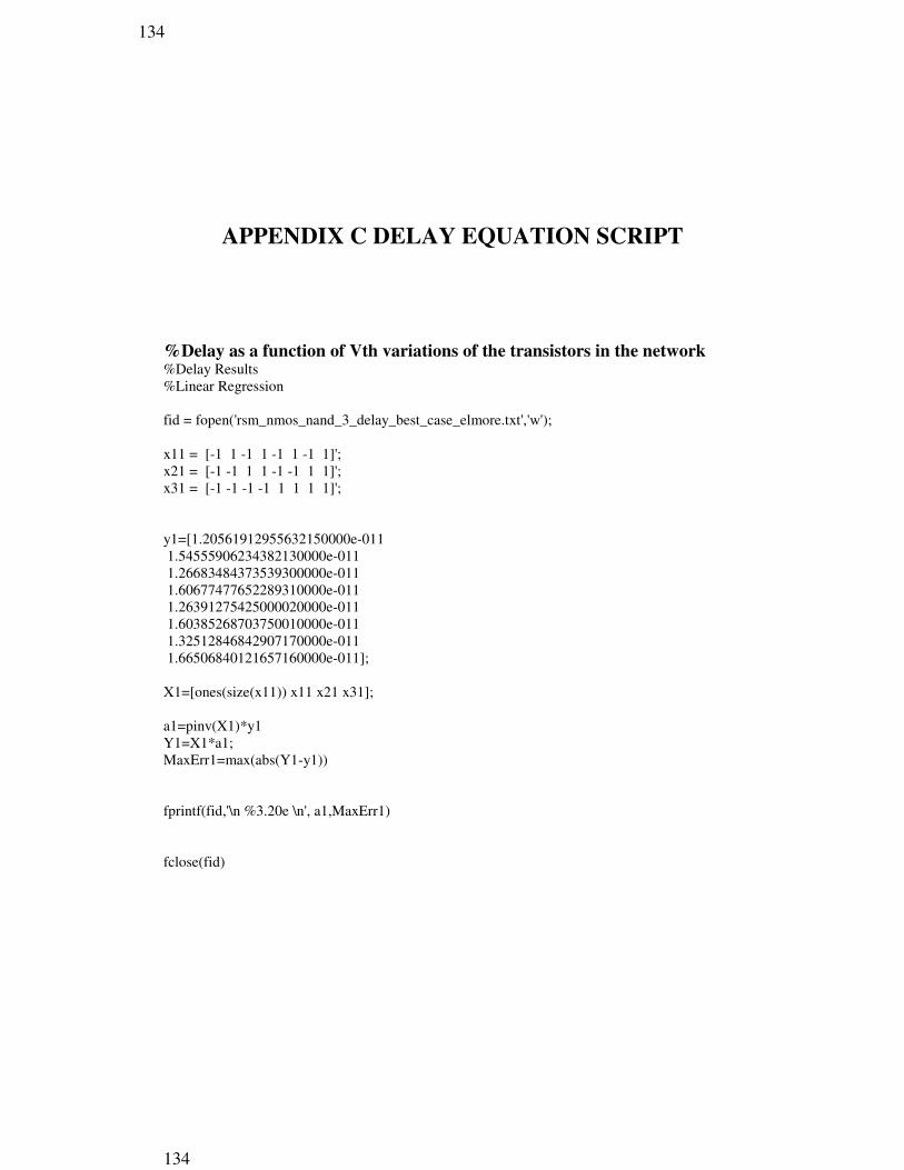
134
134
APPENDIX C DELAY EQUATION SCRIPT
%Delay as a function of Vth variations of the transistors in the network%Delay Results%Linear Regression
fid = fopen('rsm_nmos_nand_3_delay_best_case_elmore.txt','w');
x11 = [-1 1 -1 1 -1 1 -1 1]';x21 = [-1 -1 1 1 -1 -1 1 1]';x31 = [-1 -1 -1 -1 1 1 1 1]';
y1=[1.20561912955632150000e-011 1.54555906234382130000e-011 1.26683484373539300000e-011 1.60677477652289310000e-011 1.26391275425000020000e-011 1.60385268703750010000e-011 1.32512846842907170000e-011 1.66506840121657160000e-011];
X1=[ones(size(x11)) x11 x21 x31];
a1=pinv(X1)*y1Y1=X1*a1;MaxErr1=max(abs(Y1-y1))
fprintf(fid,'\n %3.20e \n', a1,MaxErr1)
fclose(fid)

135
APPENDIX D RESUMO DA TESE EM PORTUGUÊS
Método de Estimativa da Variabilidade doAtraso de Portas Lógicas em Tecnologia
CMOS

136
136
INTRODUÇÃO
Qualquer processo de produção apresenta um certo grau de variabilidade em tornodo valor nominal das especificações do produto. Este fenômeno se traduz na descriçãodas características do produto na forma de uma faixa de variação aceitável para cada umdos seus parâmetros críticos. A redução das dimensões da tecnologia MOS faz com quea variabilidade intrínseca em sua fabricação aumente. As tolerâncias de processo não seescalam proporcionalmente com as dimensões de concepção, fazendo com que oimpacto relativo das variações de dimensão crítica aumente a cada geração de novastecnologias (ARGAWAL, 2007). Este cenário exige abordagens realistas que sãocapazes de prever o impacto das variações dos parâmetros nas métricas do circuito.
Uma vez que as variações de processo tornam-se uma questão mais crítica, atransição de uma análise determinística para uma análise estatística de projetos decircuitos pode reduzir o conservadorismo da abordagem tradicional. A técnicatradicional de análise estática de atraso (STA) é uma forma razoável de se lidar com asvariações globais, mas não as locais. No caso do desempenho de um circuito, uma portalógica pode tornar-se mais lenta para uma certa variação de parâmetros e mais rápidapara outra variação, o que pode depender de sua localização em um circuito. Não apenasa importância das variações intra-die tem crescido, mas também o número deparâmetros de processo que apresentam variações consideráveis também aumentou(Srivastava, 2005).
Diferentes redes de transistores apresentam diferentes características elétricas, aindaque representem a mesma função lógica (ROSA, 2008). Nesse sentido, o objetivo destetrabalho é propor um método de estimativa de atraso que leva em conta a variabilidadeda tensão de limiar de transistores em uma rede específica. O primeiro passo foi analisarcomo a variabilidade dos parâmetros afeta as métricas das portas lógicas de acordo com(i) a topologia (a quantidade de transistores em série e em paralelo) e (ii) a posição dotransistor com um sinal de entrada transitória em relação ao nó de saída. Simulaçõeselétricas das portas foram realizadas com HSPICE, um simulador de circuito que éconsiderado referência para os circuitos elétricos. Um método de estimativa para avariação de atraso foi proposto e avaliado. Procurou-se desenvolver um método simplesde se estimar a variabilidade de atraso, levando-se em consideração diferentes portaslógicas e diferentes arranjos de transistores. O método inclui a utilização do modelo deatraso de Elmore (ELMORE, 1948) e a Avaliação de Forma de Onda Assintótica(AWE) (PILLAGE, 1990), considerando-se as resistências dos transistores obtidos emfunção de variações de tensão de limiar de transistores no arranjo. As resistências ecapacitâncias são funções dos parâmetros dos transistores. Os dados coletados atravésde simulação elétrica são comparados aos resultados gerados pelo método proposto. Os

137
resultados da análise podem ser utilizados para se alcançar implementações do circuitoque são relativamente imunes à variabilidade.
138
138
PROJETO DIGITAL E VARIABILIDADE DEPARÂMETROS EM CIRCUITOS INTEGRADOS
As portas lógicas de um circuito são constituídas basicamente por transistoresconectados a fim de se realizar uma função lógica. De uma forma bastante simplicada,um transistor pode ser concebido como um interruptor controlado pelo sinal aplicado aoterminal de porta. Um transistor NMOS está "ligado" quando o sinal de controle éelevado e "desligado" quando o sinal de controle é baixo. Um transistor PMOS age nosentido oposto, sendo "ligado" quando o sinal é baixo e "desligado" quando o sinal éalto.
Uma rede de transistor é um conjunto de dispositivos interligados atuando comochaves para implementar determinadas funções booleanas. Diferentes equaçõesbooleanas podem representar a mesma função booleana. A questão da síntese lógica édescobrir a melhor equação para uma função lógica dada. Os critérios de otimização doprojeto de um circuito estão relacionados à aplicação da equação de portas lógicas epodem ser destinados a minimizar algumas características do circuito, como área,consumo de energia ou atraso de propagação.
Um circuito pode ter suas características melhoradas através da otimização das suasredes de transistor. A otimização da rede pode ser alcançada através da reorganizaçãodos dispositivos de acordo com algumas regras para minimizar um determinado custo.No caso de se tentar reduzir o atraso de propagação em um circuito, pode acontecer quealguns sinais em blocos de lógica combinacional são mais críticos do que outros e nemtodas as entradas de uma porta transicionam ao mesmo tempo. Colocar os transistoresque estão no caminho crítico mais próximos da saída da porta pode resultar em umaredução do tempo de propagação do sinal.
A preocupação principal deste trabalho é realizar implementações que resultem ematraso de propagação de sinal com elevada imunidade às variações nos parâmetros dosdispositivos.
Fluxo de Projeto de Células-Padrão
Um fluxo de projeto é um conjunto sistemático de procedimentos que possibilita aimplementação de um chip de acordo com as especificações de uma forma que se eviteerros. Concepção de ASIC digital começa a nível comportamental e, em seguida, passapara o nível estrutural (portas e registradores), que é chamado de Register Transfer
Level (RTL), usando uma linguagem de descrição de hardware (HDL). Ferramentas desíntese lógica traduzem módulos descritos em uma linguagem HDL gerando assim um

139
netlist, que é uma descrição das células-padrão a ser usadas mais as conexões elétricasnecessárias entre elas. Como parte da etapa de síntese lógica, o mapeamentotecnológico é o processo de se implementar uma determinada rede booleana em termosde células lógicas ou portas. Normalmente, visa-se à utilização otimizada das portaslógicas de uma biblioteca para se implementar um circuito com menor atraso em seucaminho e menor área possível. As técnicas mais comuns para o mapeamentotecnológico baseiam-se em bibliotecas de células pré-caracterizadas.
Variabilidade em Circuitos IntegradosUma maneira de se classificar as variações em um circuito é de acordo com a
natureza da variação (Srivastava, 2005): (i) variações de processo, (ii) variaçõesambientais e (iii) variações de modelamento.
Variabilidade de Parâmetros de Processo
Os parâmetros de transistores que são mais suscetíveis à variações são o número e adistribuição dos átomos dopantes, o comprimento efetivo do canal do transistor, alargura e a espessura do óxido de porta. No caso de interconexões, a largura e aespessura da linha de metal são os parâmetros que sofrem maiores variações.
Variabilidade das Características dos Dispositivos
A tensão de limiar do dispositivo (VTH) é um parâmetro determinado pelo materialque implementa a porta (gate), pela espessura da camada de dióxido de silício, pelaconcentração e pelo perfil da densidade dos átomos dopantes no canal do transistor,entre outras características do processo. VTH é principalmente afetada pela variação nonúmero e na distribuição dos átomos dopantes ao longo do material e as variações naespessura do óxido. Conforme os dispositivos diminuem drasticamente de tamanho, onúmero de átomos dopantes por transistor pode ser inferior a cem, o que diminui o nívelde controle do número e da uniformidade desses átomos ao longo do canal. Nestaescala, um único átomo dopante pode alterar as características do dispositivo, resultandoem grandes variações de dispositivo para dispositivo (ORSHANSKY, 2008).

140
140
ANÁLISE DE ATRASO
Este capítulo revisa o conceito de análise de atraso estática (STA). O uso demodelos estatísticos de análise de atraso (análise de atraso estática e estatística - SSTA)também é apresentada. Esses conceitos são importantes para se compreender o objetivodesta tese, que visa à concepção de um método para avaliar as características estatísticasde redes a nível de células lógicas para ser usado em nível de circuito. A intenção destecapítulo é fornecer o contexto no qual o trabalho está inserido e para mostrar alguns dosrecentes esforços para lidar com variabilidade em projeto digital.
Statistiscal Static Timing Analysis (SSTA)A extensa pesquisa sobre análise de atraso em circuitos lógicos mostra a necessidade
de um novo método que seja capaz de lidar com as seguintes questões (ARGAWAL,2003): (i) a capacidade de controlar os parâmetros críticos do dispositivo tornam-selimitado, uma vez que as dimensões de processo continuam a encolher, o que resulta emvariações significativas destes parâmetros, (ii) o número total de parâmetros de processoque apresentam variações aumentou, fazendo com que o número de “corners” (valoresque especificam as características da porta para cada condição de processo) aumentarárapidamente, (iii) variações intra-die tornaram-se uma componente significativa davariação total, e (iv) além dos parâmetros do dispositivo, os parâmetros de interconexãodevem ser considerados.
A formulação determinística da análise de tempo trata o atraso das portas ecaminhos como números fixos, reduzindo assim um problema probabilístico a umproblema aritmético. Em SSTA as métricas de desempenho das portas lógicas e dasinterconexões são modelados a partir de valores estocásticos, resultando em funções dedensidade de probabilidade (PDF). Na análise estatística não há sentido em se tentaridentificar um único caminho do circuito como sendo o caminho crítico, ou o caminhocom o máximo de atraso. Caminhos críticos são, então, definidos como um conjunto decaminhos com alta probabilidade de se tornarem o caminho mais lento no circuito(SRIVASTAVA, 2005).

141
PROPOSTA E METODOLOGIA
Introdução
O desempenho e o consumo de energia de um circuito integrado é afetado pelasvariações do processo de fabricação (comprimento e largura do canal, espessura doóxido de porta, concentração e distribuição de átomos dopantes etc). Em relação aoprocesso de fabricação MOS, os efeitos das variações não escalam proporcionalmentecom as dimensões de concepção, fazendo com que o impacto relativo das variações dedimensão crítica aumentem a cada nova tecnologia (MAHMOODI, 2005).
Os parâmetros físicos são suscetíveis a variações aleatórias e a natureza estatísticadas características do processo faz com que seja possível considerar os parâmetros doprocesso e suas variações como variáveis aleatórias representadas pela suas funções dedensidade de probabilidade (PDF). Em (MAHMOODI, 2005) as PDFs dos atrasos deportas lógicas são estimadas considerando-se as variações de tensão de limiar devido àsflutuações aleatórias dos átomos dopantes. O desvio padrão da tensão de limiar émodelado como dependente das dimensões dos transistores (comprimento do canal elargura, espessura do óxido de porta etc) e da concentração de dopantes.
Os objetivos gerais do presente trabalho são: (i) a análise da variabilidade do atrasode diferentes redes de transistores e (ii) a concepção de um método capaz de estimar avariabilidade de determinadas topologias sem a necessidade de se fazer uso desimulações computacionalmente caras. A primeira parte do estudo se baseia emsimulações estatísticas (Monte Carlo), e destina-se a lançar uma luz sobre ocomportamento da variabilidade do desempenho de estruturas básicas de transistores ede portas lógicas. A segunda parte, principal foco deste trabalho, é a implementação deum método semi-empírico que descreve e prediz a variabilidade de acordo comdiferentes arranjos de transistores.

142
142
VARIABILIDADE NA PERFORMANCE DE PORTASLÓGICAS CMOS
Introdução
As análises apresentadas neste capítulo são resultados da pré-caracterização dealgumas células lógicas e compreendem a primeira etapa deste trabalho. Ascaracterizações proporcionaram um conhecimento inicial sobre o comportamento dasredes sob o efeito de variações de tensão de limiar de seus transistores. Esta informaçãopode ser útil no desenvolvimento de diretrizes de projeto para a melhoria de rendimentoparamétrico. Foi avaliado o impacto das variações na tensão de limiar do transistor nocomportamento do atraso de portas lógicas CMOS, de acordo com (i) a topologia darede (arranjos de transistores) e (ii) a posição relativa do transistor que possui um sinaltransiente em sua entrada em relação à fonte de alimentação e aos terminais de saída.
Simulações elétricas foram realizadas a fim de mostrar a variabilidade no atraso deum inversor CMOS, e portas lógicas NAND, NOR e AOI (AND-OR-INVERSOR). Astensões de limiar (VTH) dos transistores foram variadas e as medidas de atraso foramrealizadas para todas as configurações. O atraso médio e desvio padrão das portaslógicas foram comparados e a relação desses valores com a rede de transistor foienfatizada. Os atrasos de subida e descida das portas - inversor, NAND e NOR de 2, 3 e4 entradas, e configurações AOI-21 e AOI-32 - foram verificadas a partir de simulaçõesestatísticas (Monte Carlo). Dez mil simulações foram realizadas para cada experimento.As medidas foram feitas para um desvio 3σ de 10% da tensão de limiar nominal dostransistores. Os valores de desvio padrão normalizado (σ/µ) das métricas das diferentesconfigurações foram comparados e analizados. O desvio padrão normalizado tornapossível comparar a variabilidade de arranjos com diferentes valores médios de atraso.O nó tecnológico utilizado neste trabalho é de 45 nm e o arquivo de modelo inserido nonetlist das simulações foi fornecido pelo Predictive Tecnology Model (PTM) (ZHAO,2007), com base no BSIM4. Nenhuma correlação entre os diferentes tipos detransistores foi levada em consideração, o que significa que um PMOS colocado naproximidade de um NMOS pode apresentar variações diferentes de um mesmoparâmetro. As simulações foram realizadas utilizando-se a ferramenta HSPICE.

143
MÉTODO DE ESTIMATIVA DA VARIABILIDADE DEATRASO
O presente trabalho propõe a implementação de um método capaz de prever avariabilidade no atraso de uma porta lógica. Uma única variável - a variação da tensãolimiar – é atribuída a cada transistor da porta lógica analisada. Sempre que possível, aporta é dividida em redes pull-up e pull-down, o que reduz o número de dispositivos evariáveis com os quais se é preciso lidar.
O método de fatoriais (MYERS, 2002) é utilizado para se identificar os principaisefeitos dos fatores (∆VTH) sobre as primeiras variáveis-alvo, ou seja, sobre asresistências dos transistores. Uma vez que a cada variável de interesse são atribuídosdois níveis (valores codificados -1 e +1), cada variante de tal projeto tem 2k simulaçõesDC a serem executadas, o que é chamado de projeto fatorial 2k, onde 'k' é o número detransistores na porta lógica a ser analisada ('k' limiares de tensão).
Inicialmente, simulações elétricas do tipo DC são realizadas para extrair as'resistências-ON" de transistores para diferentes tensões de limiar (∆VTH) de acordocom a metodologia de 2k casos. O VTH de transistores são variados em ± 10% de seusvalores nominais e transformados em variáveis codificadas (normalizadas) com valores-1 e +1, que representam os valores mínimo e máximo assumidos pela VTH,respectivamente. Para o exemplo apresentado na Figura 6.1, as resistências sãofornecidas por 23 (sendo três transistores) simulações DC, dividindo-se a queda detensão em cada transistor pela corrente que passa através dele.
O efeito estimado em um método fatorial com 2k casos é então convertido em ummodelo de regressão (função de primeira ordem para a resistência do dispositivo), quepode ser usado para analisar a resposta (resistência) em qualquer ponto do espaçogerado pelos fatores codificados (∆VTH) no projeto.
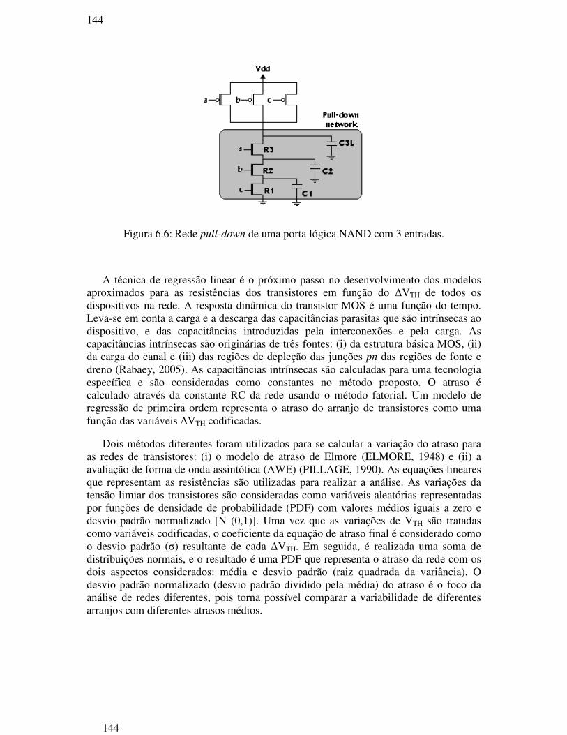
144
144
Figura 6.6: Rede pull-down de uma porta lógica NAND com 3 entradas.
A técnica de regressão linear é o próximo passo no desenvolvimento dos modelosaproximados para as resistências dos transistores em função do ∆VTH de todos osdispositivos na rede. A resposta dinâmica do transistor MOS é uma função do tempo.Leva-se em conta a carga e a descarga das capacitâncias parasitas que são intrínsecas aodispositivo, e das capacitâncias introduzidas pela interconexões e pela carga. Ascapacitâncias intrínsecas são originárias de três fontes: (i) da estrutura básica MOS, (ii)da carga do canal e (iii) das regiões de depleção das junções pn das regiões de fonte edreno (Rabaey, 2005). As capacitâncias intrínsecas são calculadas para uma tecnologiaespecífica e são consideradas como constantes no método proposto. O atraso écalculado através da constante RC da rede usando o método fatorial. Um modelo deregressão de primeira ordem representa o atraso do arranjo de transistores como umafunção das variáveis ∆VTH codificadas.
Dois métodos diferentes foram utilizados para se calcular a variação do atraso paraas redes de transistores: (i) o modelo de atraso de Elmore (ELMORE, 1948) e (ii) aavaliação de forma de onda assintótica (AWE) (PILLAGE, 1990). As equações linearesque representam as resistências são utilizadas para realizar a análise. As variações datensão limiar dos transistores são consideradas como variáveis aleatórias representadaspor funções de densidade de probabilidade (PDF) com valores médios iguais a zero edesvio padrão normalizado [N (0,1)]. Uma vez que as variações de VTH são tratadascomo variáveis codificadas, o coeficiente da equação de atraso final é considerado comoo desvio padrão (σ) resultante de cada ∆VTH. Em seguida, é realizada uma soma dedistribuições normais, e o resultado é uma PDF que representa o atraso da rede com osdois aspectos considerados: média e desvio padrão (raiz quadrada da variância). Odesvio padrão normalizado (desvio padrão dividido pela média) do atraso é o foco daanálise de redes diferentes, pois torna possível comparar a variabilidade de diferentesarranjos com diferentes atrasos médios.

145
MODELAMENTO DA VARIABILIDADE DE ATRASO DEREDES DE TRANSISTORES
Este capítulo apresenta os resultados obtidos utilizando-se o método de estimativaproposto para o cálculo do desvio do atraso das diferentes redes de transistores.Simulações elétricas do tipo DC foram realizadas com HSPICE. Os outros cálculosforam realizados com a ferramenta MATLAB ® (Matrix Laboratory).
Em uma topologia com transistores NMOS em série, o transistor mais próximo donó de saída tem uma resistência maior do que os outros quando todos os dispositivossão considerados como ligados (conduzindo corrente). Embora a tensão da porta deentrada esteja no mesmo nível para todos os dispositivos, o mesmo não acontece com atensão porta-fonte. No caso de um arranjo em série, os dispositivos têm as suas fontescom um potencial igual a VDD - VTH, exceto para o dispositivo na parte inferior doempilhamento, que tem sua fonte ligada ao nó terra. O terminal de fonte dosdispositivos no topo do empilhamento passa mais tempo perto de VDD - VTH e menostempo conduzindo fortemente do que os outros dispositivos. Isso resulta em um VTH
efetivo maior devido ao efeito de corpo, o que resulta em maior resistência efetiva.
O uso do modelo de atraso de Elmore (ELMORE, 1948) permite realizar umaoperação de soma direta de PDFs para calcular as resistências equivalentes das redes detransistores, e em seguida a constante de tempo RC. O método de avaliação de forma deonda assintótica (AWE) requer o cálculo das matrizes de condutâncias e decapacitâncias a partir das equações de estado do circuito considerado. A partir dasmatrizes, os momentos são encontrados e combinados via aproximação de Padé,resultando em modelos de forma reduzida. Em ambos os métodos, é necessário calcularo atraso para os valores de casos (casos fatoriais) de x1, x2, x3 e x4 (coded ∆VTH) eajustar uma equação.
Simulações anteriores com transistores NMOS em série revelaram menor desvio deatraso para o caso em que o transistor que possui um sinal transiente em sua entrada estápróximo do nó de saída do que para o caso em que o transistor se encontra longe do nóde saída. Para uma arranjo com transistores PMOS em série, maior imunidade àvariação das tensões de limiar é obtida quando o transistor de chaveamento está longedo terminal de saída. Os modelos semi-empíricos obtidos para as resistências eutilizados para calcular o desvio do atraso nas redes também mostraram a mesmatendência para a PMOS, mas não para a rede NMOS.
Os resultados revelaram que, em geral, a posição do transistor que chaveia impactamais fortemente os arranjos em série NMOS do que os arranjos em série PMOS. O

146
146
modelo proposto para as resistências dos transistores em uma rede permite investigarcomo as variações na tensão de limiar de cada dispositivo influenciam as resistências detodos os dispositivos do arranjo. Ao se utilizar as funções de resistência também épossível analisar a variabilidade do desempenho de acordo com o estado e posição dosdispositivos na rede. Apesar do modelo de atraso de Elmore apresentar algumaslimitações, ele é plausível de ser utilizado para se realizar a análise.

147
AVALIAÇÃO DO MÉTODO DE ESTIMATIVA DAVARIABILIDADE DE ATRASO
Neste capítulo, o método de estimativa proposto foi utilizado para avaliar o desviode atraso de portas implementadas em diferentes topologias e estilos lógicos. O caminhode propagação do sinal foi simplificado a fim de se aplicar as resistências para o modelode atraso de Elmore (ELMORE, 1948) no cálculo da variação do atraso. Isso foi feitoatravés da substituição das resistências em paralelo por uma resistência equivalente. Atécnica de AWE (Pillage 1990) foi também utilizada em alguns casos. As célulastestadas compreendem uma porta lógica XOR de 2 entradas (XOR2), uma XOR de 4entradas (XOR4) e um somador completo, que são estruturas usadas em bibliotecas decélulas para o mapeamento tecnológico.
Porta Lógica XOR de 2 EntradasA XOR de 2 entradas foi implementada em diferentes topologias, como mostrado na
figura. 8.1. O dimensionamento dos transistores foi realizado de forma a equilibrar acapacidade de corrente das diferentes redes através do projeto de dispositivos PMOScom área duas vezes maior do que a área dos dispositivos NMOS. O método proposto éusado para fornecer valores de variação no atraso. Simulações estatísticas Monte Carlotambém foram realizadas para efeito de comparação. O objetivo é investigar como ométodo é confiável em prever a topologia a ser escolhida (ou ignorada) quando umaconfiguração mais robusta (com menor variação de atraso) é desejada. As configuraçõesconsideradas são: (i) uma única porta CMOS complexa, (ii) uma implementação com 4portas NAND e (iii) uma implementação usando a lógica de transistor de passagem.
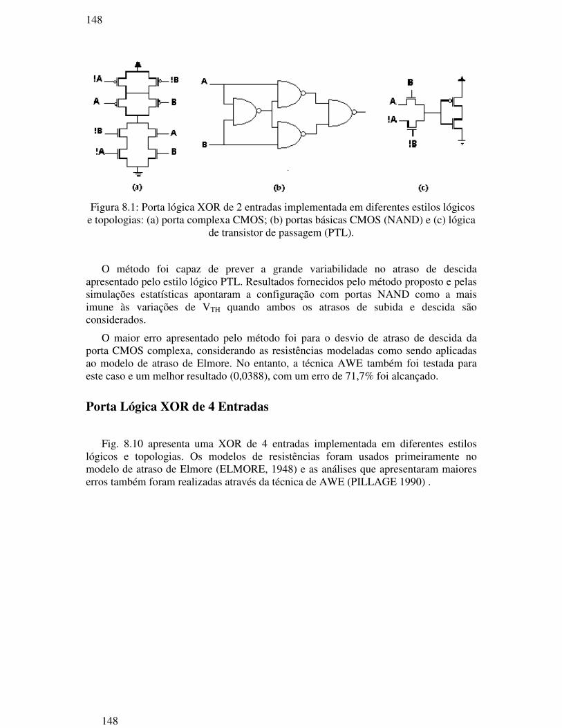
148
148
Figura 8.1: Porta lógica XOR de 2 entradas implementada em diferentes estilos lógicose topologias: (a) porta complexa CMOS; (b) portas básicas CMOS (NAND) e (c) lógica
de transistor de passagem (PTL).
O método foi capaz de prever a grande variabilidade no atraso de descidaapresentado pelo estilo lógico PTL. Resultados fornecidos pelo método proposto e pelassimulações estatísticas apontaram a configuração com portas NAND como a maisimune às variações de VTH quando ambos os atrasos de subida e descida sãoconsiderados.
O maior erro apresentado pelo método foi para o desvio de atraso de descida daporta CMOS complexa, considerando as resistências modeladas como sendo aplicadasao modelo de atraso de Elmore. No entanto, a técnica AWE também foi testada paraeste caso e um melhor resultado (0,0388), com um erro de 71,7% foi alcançado.
Porta Lógica XOR de 4 Entradas
Fig. 8.10 apresenta uma XOR de 4 entradas implementada em diferentes estiloslógicos e topologias. Os modelos de resistências foram usados primeiramente nomodelo de atraso de Elmore (ELMORE, 1948) e as análises que apresentaram maioreserros também foram realizadas através da técnica de AWE (PILLAGE 1990) .

149
Figure 8.10: 4-input XOR implemented in different logic styles: (a) differential cascodevoltage logic (DCVSL) and (b) pass-transistor logic (PTL).
Os melhores resultados (mais próximos dos valores simulados) apresentados pelométodo foram encontrados para o estilo DCVSL, considerando-se ambos os atrasos desubida e descida. O método foi capaz de prever a configuração menos robusta entre asque foram utilizadas para implementar a porta XOR de 4 entradas. O maior erroapresentado pelo modelo foi para o desvio de atraso de descida do estilo DPTLconsiderando-se as resistências aplicadas ao modelo de atraso de Elmore. No entanto, ométodo foi testado com a técnica AWE para este caso e um melhor resultado (0,1314)foi alcançado, apresentando um erro de apenas 10,3%.
Somador CompletoO somador completo é uma célula lógica com três entradas e duas saídas (Weste
2005).

150
150
Figura 8.18: Somador completo implementado em diferentes estilos lógicos: (a) portacomplexa CMOS; (b) lógica diferencial de transistores de passagem (DPTL).
A rede NMOS da porta CMOS complexa é mais suscetível às variações de tensão delimiar que a rede PMOS, como visto no CAPÍTULO 7. O método proposto está deacordo com os resultados da simulação no se refere ao desvio do atraso de descida,mostrando que a topologia DPTL é a menos robusta dentre as topologias analisadas.
O erro apresentado pelo método quanto ao desvio de atraso de descida do estiloDPTL considerando as resistências aplicadas ao modelo de atraso Elmore foi reduzidopara 17,2% quando as resistências foram utilizados com a técnica AWE. Neste caso, odesvio foi 0,1016.
Análise do Tempo de SimulaçãoA caracterização das portas lógicas a partir de simulações estatísticas Monte Carlo é
computacionalmente cara e leva muito tempo para ser completada, o que a tornaproibitiva em alguns casos. A abordagem apresentada neste trabalho para caracterizar ascélulas requer simulações que levam apenas alguns segundos, uma vez que apenas umasimulação é transiente e todas as outras são DC.
Método da Equação de AtrasoO aqui chamado Método da Equação de Atraso (DEM) também usa o método dos
mínimos quadrados a fim de obter os coeficientes do modelo de primeira ordem(equação) do atraso como uma função das variações de tensão de limiar dos transistores.A diferença desse método em relação ao método de estimativa proposto neste trabalho éque, basicamente, o primeiro exige simulações transientes ao invés de simulações dotipo DC. Nesse sentido, o DEM não utiliza a constante RC da rede a fim deproporcionar o atraso da célula lógica, pois o atraso é a métrica diretamente fornecidapelas simulações transientes.

151
Variações deste método já estão disponíveis na literatura (OKADA 2003) e é porisso que a análise fornecida pelo método de estimativa proposto é comparado com oDEM neste capítulo.

152
152
CONCLUSÃO
Diferentes topologias de inversores apresentam diferentes desvios de atraso quandoas tensões de limiar dos transistores variam. A análise preliminar com base emsimulações Monte Carlo mostrou que a escolha da topologia e estilo lógico, o númerode transistores na rede e a posição dos transistores com sinais transientes no terminal deentrada influenciam a variabilidade de atraso da célula lógica. Quando apenas uma partedo arranjo de transistores é analisada, como o pull-up ou pull-down em umaconfiguração CMOS, por exemplo, melhores resultados (desvio de atraso menor) foramalcançados para um maior número de transistores no arranjo.
O método de estimativa da variabilidade proposto foi aplicado principalmente paraconfigurações MOS complementares (CMOS), mas também apresentou resultadosimportantes para os estilos lógicos DCVSL, PTL e DPTL. Para compor o método, aresistência de cada transistor foi calculada em função das variações de tensão de limiarde todos os dispositivos na rede. Cada topologia requer 2.2k simulações elétricas DC, oque leva menos de 10 segundos, mesmo para portas lógicas com mais de 10 transistores.A análise de duas regiões diferentes de operação - linear e saturação - a fim de atingir osvalores de resistências mostraram que a região linear fornece funções de resistênciamais confiáveis.
A análise de redes com transistores em série e paralelo revelou diferençassignificativas quando dispositivos N- ou PMOS compõem o arranjo. Redes NMOS têmdesvios de atraso que são mais sensíveis às variações na tensão limiar dos transistores.Em geral, um número mais elevado de transistores MOS em uma topologia em série,torna a configuração mais robusta. Em uma rede paralela pura, variações na tensão delimiar de transistores que não estão conduzindo não têm nenhuma influência sobre avariabilidade do atraso.
No caso dos inversores concebidos a partir de diferentes topologias, quando o desvioVTH é alterado de acordo com as dimensões dos transistores (de acordo com o modelode Pelgrom), torna-se evidente que dispositivos MOS com maior área resultam emmenor variabilidade de atraso.
Resultados fornecidos pelas simulações estatísticas, bem como pelo métodoproposto mostraram que, para uma cadeia de inversores, quanto maior o número deinversores, menores os desvios dos atrasos de subida e descida. Finalmente, acomparação entre diferentes topologias e estilos lógicos usados para se implementar amesma função lógica - uma XOR de 2 entradas - mostrou que o atraso da configuraçãocom portas NAND sofre menos influência das variações das tensões de limiar dostransistores. A lógica de transistor de passagem foi a que apresentou maior desvio de

153
atraso dentre as topologias analisadas. A portas lógicas também foram analisadas com ométodo proposto, que forneceu resultados compatíveis com as simulações estatísticas.No caso de uma XOR de 4 entradas, a porta implementada no estilo DCVSL aparececomo a configuração mais confiável dentre as analisadas. Para se implementar umsomador completo, a porta complexa CMOS é preferível sobre o estilo DPTL, quando oatraso do nó de saída "SUM" é analisado.
A fim de se proporcionar a função densidade de probabilidade do atraso de umatopologia, o método proposto exige um tempo de execução que é de cerca de 3.000vezes menor que o tempo exigido pelas simulações Monte Carlo (10.000 execuções).