an abstract of the thesis of - oregon state...
TRANSCRIPT


AN ABSTRACT OF THE THESIS OF
Rick E. Presley for the degree of Master of Science in
Electrical Engineering and Computer Science presented on February 27, 2006.
Title: Transparent Electronics: Thin-Film Transistors and Integrated Circuits
Abstract approved:
John F. Wager
This thesis focuses on two aspects of transparent electronics, SnO2 transpar-
ent thin-film transistors (TTFTs) and transparent circuits. Both depletion- and
enhancement-mode SnO2 TTFTs are realized. The maximum effective mobility for
the depletion- and enhancement-mode devices are 2 cm2V−1s−1 and 0.8 cm2V−1s−1,
respectively. A variety of techniques to decrease the carrier concentration in the SnO2
channel are investigated. However, the only successful technique is to decrease the
channel thickness, which effectively decreases the channel conductivity, and is the
procedure employed for successful realization of an enhancement-mode TTFT.
The second part of this thesis focuses on the fabrication procedure and the
electrical characteristics of transparent circuits, which include inverters and ring os-
cillators. These circuits are highly transparent, exhibiting ∼75% optical transmit-
tance in the visible portion of the electromagnetic spectrum, and are fabricated using
indium gallium oxide as the active channel material and standard photolithography
techniques. The n-channel indium gallium oxide thin-film transistors exhibit a peak
incremental mobility of ∼7 cm2V−1s−1 and a turn-on voltage of ∼2 V. A five-stage
ring oscillator circuit (which does not employ level-shifting) is fabricated, and exhibits
an oscillation frequency of ∼2.2 kHz with the gate and drain of the load transistor

biased at 30 V; the maximum oscillation frequency observed is ∼9.5 kHz, with the
gate and drain of the load transistor biased at ∼80 V.

c©Copyright by Rick E. Presley
February 27, 2006
All rights reserved
Transparent Electronics: Thin-Film Transistors and Integrated Circuits
by
Rick E. Presley
A THESIS
submitted to
Oregon State University
in partial fulfillment ofthe requirements for the
degree of
Master of Science
Completed February 27, 2006Commencement June 2006

Master of Science thesis of Rick E. Presley presented on February 27, 2006
APPROVED:
Major Professor, representing Electrical Engineering and Computer Science
Director of the School of Electrical Engineering and Computer Science
Dean of the Graduate School
I understand that my thesis will become part of the permanent collection of OregonState University libraries. My signature below authorizes release of my thesis to anyreader upon request.
Rick E. Presley, Author

ACKNOWLEDGMENT
I would like to thank my major professor, Dr. John F. Wager for providing the
opportunity to work on this research topic and providing the funding and support for
this research. Without this funding and support this research could not have been
completed.
I would also like to thank Hai Chiang and David Hong for all the helpful
discussions and providing training on the equipment. I would like to thank Robert
Kykyneshi from the physics department at Oregon State University with providing
the optical measurements presented in this thesis. I would like to acknowledge Chris
Tasker, who keeps the lab running, and Manfred Dittrich for making shadow masks
and other parts used to complete this work.
This work was funded by the U. S. National Science Foundation under Grant
No. DMR-0245386, by the Army Research Office under Contract No. MURI E-18-
667-G3, and by the Hewlett-Packard Company.

TABLE OF CONTENTS
Page
1. INTRODUCTION . . . . . . . . . . . . . . . . . . . . . . . . . . . . . . . . . . . . . . . . . . . . . . . . . . . . . . . 1
2. LITERATURE REVIEW . . . . . . . . . . . . . . . . . . . . . . . . . . . . . . . . . . . . . . . . . . . . . . . 3
2.1 Thin-film transistor operation . . . . . . . . . . . . . . . . . . . . . . . . . . . . . . . . . . . . . . 3
2.2 Inverter operation. . . . . . . . . . . . . . . . . . . . . . . . . . . . . . . . . . . . . . . . . . . . . . . . . . 5
2.3 Ring oscillator operation . . . . . . . . . . . . . . . . . . . . . . . . . . . . . . . . . . . . . . . . . . . 6
2.4 Previous reported TFTs based on wide band gap semiconductors . . . 10
2.4.1 ZnO based thin-film transistors . . . . . . . . . . . . . . . . . . . . . . . . . . . . . 112.4.2 Tin oxide based thin-film transistors . . . . . . . . . . . . . . . . . . . . . . . . 122.4.3 Indium gallium zinc oxide thin-film transistors . . . . . . . . . . . . . . 132.4.4 Zinc tin oxide thin-film transistors . . . . . . . . . . . . . . . . . . . . . . . . . . 142.4.5 Thin-film transistors fabricated using zinc indium oxide . . . . . 14
2.5 Tin oxide material properties and conventional applications . . . . . . . . 14
2.5.1 Tin oxide as a transparent interconnect . . . . . . . . . . . . . . . . . . . . . 162.5.2 Tin oxide as a gas sensor . . . . . . . . . . . . . . . . . . . . . . . . . . . . . . . . . . . . 172.5.3 Tin oxide as a window coating . . . . . . . . . . . . . . . . . . . . . . . . . . . . . . 17
2.6 Pentacene organic ring oscillators . . . . . . . . . . . . . . . . . . . . . . . . . . . . . . . . . . 18
2.7 Conclusions . . . . . . . . . . . . . . . . . . . . . . . . . . . . . . . . . . . . . . . . . . . . . . . . . . . . . . . . 21
3. EXPERIMENTAL TECHNIQUE . . . . . . . . . . . . . . . . . . . . . . . . . . . . . . . . . . . . . . . 23
3.1 Thin film deposition techniques . . . . . . . . . . . . . . . . . . . . . . . . . . . . . . . . . . . . 23
3.1.1 Physical vapor deposition techniques . . . . . . . . . . . . . . . . . . . . . . . . 233.1.1.1 Thermal evaporation . . . . . . . . . . . . . . . . . . . . . . . . . . . . . . . . . 233.1.1.2 Activated reactive evaporation . . . . . . . . . . . . . . . . . . . . . . . 243.1.1.3 Radio frequency sputtering . . . . . . . . . . . . . . . . . . . . . . . . . . . 243.1.1.4 Direct current sputtering . . . . . . . . . . . . . . . . . . . . . . . . . . . . . 25
3.1.2 Chemical vapor deposition techniques . . . . . . . . . . . . . . . . . . . . . . . 253.1.2.1 Plasma-enhanced chemical vapor deposition . . . . . . . . . . 26
3.1.3 Etching processes . . . . . . . . . . . . . . . . . . . . . . . . . . . . . . . . . . . . . . . . . . . 273.1.3.1 Chemical etch . . . . . . . . . . . . . . . . . . . . . . . . . . . . . . . . . . . . . . . 27
TABLE OF CONTENTS (Continued)
Page
3.1.3.2 Physical etch . . . . . . . . . . . . . . . . . . . . . . . . . . . . . . . . . . . . . . . . 283.1.3.3 Reactive ion etch . . . . . . . . . . . . . . . . . . . . . . . . . . . . . . . . . . . . 28
3.1.4 Photolithography techniques . . . . . . . . . . . . . . . . . . . . . . . . . . . . . . . . 293.1.4.1 Types of photoresist . . . . . . . . . . . . . . . . . . . . . . . . . . . . . . . . . 293.1.4.2 Exposure and development . . . . . . . . . . . . . . . . . . . . . . . . . . . 293.1.4.3 Film patterning . . . . . . . . . . . . . . . . . . . . . . . . . . . . . . . . . . . . . . 29
3.2 Electrical characterization. . . . . . . . . . . . . . . . . . . . . . . . . . . . . . . . . . . . . . . . . . 31
3.2.1 Turn-on voltage . . . . . . . . . . . . . . . . . . . . . . . . . . . . . . . . . . . . . . . . . . . . . 313.2.2 Mobility . . . . . . . . . . . . . . . . . . . . . . . . . . . . . . . . . . . . . . . . . . . . . . . . . . . . 32
3.2.2.1 Incremental mobility . . . . . . . . . . . . . . . . . . . . . . . . . . . . . . . . . 323.2.2.2 Average mobility. . . . . . . . . . . . . . . . . . . . . . . . . . . . . . . . . . . . . 333.2.2.3 Saturation mobility . . . . . . . . . . . . . . . . . . . . . . . . . . . . . . . . . . 33
3.2.3 Drain current on-to-off ratio . . . . . . . . . . . . . . . . . . . . . . . . . . . . . . . . 333.2.4 Operating frequency . . . . . . . . . . . . . . . . . . . . . . . . . . . . . . . . . . . . . . . . 34
3.3 Conclusions . . . . . . . . . . . . . . . . . . . . . . . . . . . . . . . . . . . . . . . . . . . . . . . . . . . . . . . . 34
4. TIN OXIDE TRANSPARENT THIN-FILM TRANSISTORS . . . . . . . . . . . . 36
4.1 SnO2 TTFT device fabrication . . . . . . . . . . . . . . . . . . . . . . . . . . . . . . . . . . . . . 36
4.2 SnO2 TTFT electrical characteristics and discussion. . . . . . . . . . . . . . . . 36
4.3 Conclusions . . . . . . . . . . . . . . . . . . . . . . . . . . . . . . . . . . . . . . . . . . . . . . . . . . . . . . . . 42
5. TRANSPARENT CIRCUITS . . . . . . . . . . . . . . . . . . . . . . . . . . . . . . . . . . . . . . . . . . . . 43
5.1 Transparent circuit fabrication . . . . . . . . . . . . . . . . . . . . . . . . . . . . . . . . . . . . . 43
5.2 Electrical characterization and discussion. . . . . . . . . . . . . . . . . . . . . . . . . . . 45
5.3 Conclusions . . . . . . . . . . . . . . . . . . . . . . . . . . . . . . . . . . . . . . . . . . . . . . . . . . . . . . . . 51
6. CONCLUSIONS AND RECOMMENDATIONS FOR FUTURE WORK . 53
6.1 Conclusions . . . . . . . . . . . . . . . . . . . . . . . . . . . . . . . . . . . . . . . . . . . . . . . . . . . . . . . . 53
6.2 Recommendations for future work . . . . . . . . . . . . . . . . . . . . . . . . . . . . . . . . . . 54

TABLE OF CONTENTS (Continued)
Page
BIBLIOGRAPHY . . . . . . . . . . . . . . . . . . . . . . . . . . . . . . . . . . . . . . . . . . . . . . . . . . . . . . . . . . . 55
APPENDICES . . . . . . . . . . . . . . . . . . . . . . . . . . . . . . . . . . . . . . . . . . . . . . . . . . . . . . . . . . . . . . 58

LIST OF FIGURES
Figure Page
2.1 A bottom-gate thin-film transistor structure and several energy banddiagrams as viewed through the gate of the TFT. (a) TFT structure.(b) Energy band diagram when biased in equilibrium. (c) Energyband diagram when a negative voltage is applied to the gate. (d)Energy band diagram when a positive voltage is applied to the gatecontact. . . . . . . . . . . . . . . . . . . . . . . . . . . . . . . . . . . . . . . . . . . . . . . . . . . . . . . . . . . . . 4
2.2 A theoretical transfer curve and a circuit representation illustrat-ing the essential features of the inverters employed in this thesis.Both the control and load transistors are n-channel, accumulation-mode TFTs, operating in enhancement-mode, i.e., possessing posi-tive turn-on voltages. . . . . . . . . . . . . . . . . . . . . . . . . . . . . . . . . . . . . . . . . . . . . . . . 7
2.3 Schematic representation of a ring oscillator showing the voltagesand currents present at different times throughout device operation. . 8
3.1 Schematic drawing showing a parallel plate cold-wall plasma-enhancedchemical vapor deposition system. This configuration is used to de-posit silicon dioxide used as a gate insulator in the transparent circuits. 27
3.2 Pattern transfer using positive and negative photoresist. . . . . . . . . . . . . . 30
3.3 Log(ID) versus VGS plot for an IGO TFT indicating the turn-onvoltage, and leakage current/noise floor. . . . . . . . . . . . . . . . . . . . . . . . . . . . . 32
3.4 SPICE simulation output for an inverter stage, indicating how riseand fall times are measured. The solid line is the output voltage fromthe inverter. The dashed trace is the input voltage to the inverterstage, and the gray solid line indicates the switching voltage for theinverter stage. . . . . . . . . . . . . . . . . . . . . . . . . . . . . . . . . . . . . . . . . . . . . . . . . . . . . . . 35
4.1 Drain current-drain voltage (IDS-VDS) characteristics for a SnO2
TTFT with a SnO2 channel layer that is ∼10 nm thick, depositedby RF magnetron sputtering, and rapid thermal annealed in O2
at 600 ◦C. The channel length and width are 1524 µm and 7620µm, respectively. VGS is decreased from 40 V (top curve, showingmaximum current) to 0 V in 5 V steps. . . . . . . . . . . . . . . . . . . . . . . . . . . . . . 37
LIST OF FIGURES (Continued)
Figure Page
4.2 Log(IDS)-VGS and Log(IGS)-VGS characteristics at VDS = 35 V fora SnO2 TTFT with a channel width-to-length ratio of 5. Inset showsan extrapolation of the linear portion of an IDS-VGS curve, resultingin an estimated threshold voltage of VT ' 10 V. The SnO2 channellayer is ∼10 nm thick, deposited by RF magnetron sputtering, andrapid thermal annealed in O2 at 600 ◦C. . . . . . . . . . . . . . . . . . . . . . . . . . . . . 38
4.3 Optical transmittance as viewed through the ITO source/drain andthe channel of a SnO2 TTFT. Curve (a) is corrected for reflectance,i.e., T / (1 - R), whereas curve (b) is the raw transmission throughthe entire stack, including the substrate. Inset illustrates the bottom-gate TTFT structure and biasing scheme employed. . . . . . . . . . . . . . . . . . 39
4.4 X-ray diffraction patterns obtained from two sputter-deposited SnO2
thin films which are either furnace or rapid thermal annealed (RTA)at 600◦C, and for a SnO2 thin film prepared by evaporation of SnO2
powder in a ∼ 5×10⁻⁴ Torr pressure of microwave-activated N2 andsubsequently furnace annealed at 600◦C. The post-deposition annealleads to increased crystallinity of the sputtered films, whereas filmsprepared by activated reactive evaporation in N2 remain amorphousafter annealing. . . . . . . . . . . . . . . . . . . . . . . . . . . . . . . . . . . . . . . . . . . . . . . . . . . . . . 40
5.1 Schematic representation of (a) cross-sectional and (b) a plan viewfor a transparent inverter, where W1 and W2 are the widths of theload and control transistors respectively, LOV is the source/gate ordrain/gate overlap, and L is the channel length. . . . . . . . . . . . . . . . . . . . . . 44
5.2 The optical transmittance versus wavelength through the source/drain(black) and channel (grey) regions of IGO TTFTs. Both regionsexhibit average transmittance in the visible portion of the electro-magnetic spectrum of ∼75%. (Inset) Glass substrate containing tworing oscillators, three inverters, and several discrete transistors rest-ing atop the label “Transparent Circuits”. . . . . . . . . . . . . . . . . . . . . . . . . . . 45
5.3 Log(ID)-VGS transfer curves with VDS = 1 (square symbols) and20 V (triangle symbols) for an IGO TTFT. The channel width andlength for this device are 2400 and 60 µm, respectively. (Inset)Incremental mobility versus gate voltage, extracted from the ID-VGS
data with VDS = 1 V. . . . . . . . . . . . . . . . . . . . . . . . . . . . . . . . . . . . . . . . . . . . . . . 46

LIST OF FIGURES (Continued)
Figure Page
5.4 Transfer curve for a transparent inverter fabricated using IGO TTFTsand with VDD and Vload = 30 V. (Inset) Inverter gain magnitude asa function of VDD. . . . . . . . . . . . . . . . . . . . . . . . . . . . . . . . . . . . . . . . . . . . . . . . . . . 48
5.5 Oscillation frequency as a function of VDD for a five-stage ring os-cillator fabricated using IGO TTFTs. (Inset) Output characteristicof the transparent ring oscillator when VDD = Vload = 30 V. . . . . . . . . 49
5.6 Oscillation frequency as a function of the channel length for a five-stage ring oscillator via SPICE simulation using a width-to-lengthratio of 40 for the control transistor, width-to-length ratio of 10 forthe load transistor, a overlap capacitance of 70.8 nFcm−1, mobilityof 2.55 cm2V−1s−1 for both transistors, a turn-on voltage of 2 V forboth transistors, and biased at 30 V. . . . . . . . . . . . . . . . . . . . . . . . . . . . . . . . . 50
5.7 Oscillation frequency as a function of the contact overlap for a five-stage ring oscillator using SPICE with a width-to-length ratio of 40for the control transistor, a width-to-length ratio of 10 for the loadtransistor, a channel length of 60 µm, a mobility of 2.55 cm2V−1s−1
for both transistors, a turn-on voltage of 2 V for both transistors,and biased at 30 V. . . . . . . . . . . . . . . . . . . . . . . . . . . . . . . . . . . . . . . . . . . . . . . . . . 52

LIST OF TABLES
Table Page
2.1 Wide band gap-based TFTs, processing methods employed, and elec-trical performance characteristics for several different channel mate-rials. The maximum processing temperature, deposition method,mobility, drain current on-to-off ratio, and threshold voltage are in-cluded. . . . . . . . . . . . . . . . . . . . . . . . . . . . . . . . . . . . . . . . . . . . . . . . . . . . . . . . . . . . . . 15
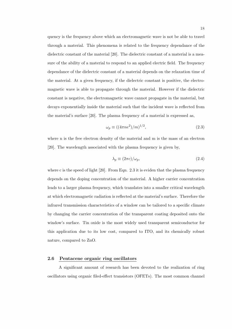
2.2 A summary of pentacene-based ring oscillator device geometry andperformance. The mobility, channel length, channel width, contactoverlap, use of level-shifting circuitry, and propagation delay areincluded. . . . . . . . . . . . . . . . . . . . . . . . . . . . . . . . . . . . . . . . . . . . . . . . . . . . . . . . . . . . 21
TRANSPARENT ELECTRONICS:THIN-FILM TRANSISTORS AND INTEGRATED CIRCUITS
1. INTRODUCTION
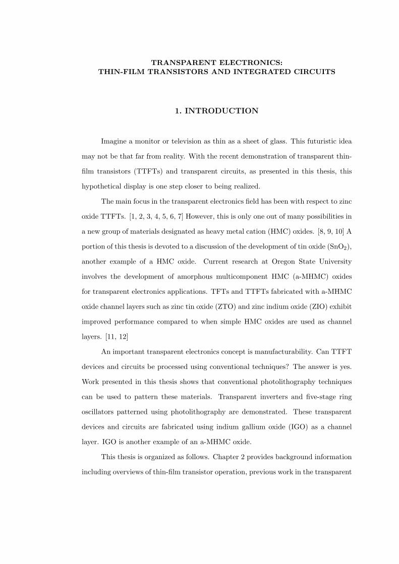
Imagine a monitor or television as thin as a sheet of glass. This futuristic idea
may not be that far from reality. With the recent demonstration of transparent thin-
film transistors (TTFTs) and transparent circuits, as presented in this thesis, this
hypothetical display is one step closer to being realized.
The main focus in the transparent electronics field has been with respect to zinc
oxide TTFTs. [1, 2, 3, 4, 5, 6, 7] However, this is only one out of many possibilities in
a new group of materials designated as heavy metal cation (HMC) oxides. [8, 9, 10] A
portion of this thesis is devoted to a discussion of the development of tin oxide (SnO2),
another example of a HMC oxide. Current research at Oregon State University
involves the development of amorphous multicomponent HMC (a-MHMC) oxides
for transparent electronics applications. TFTs and TTFTs fabricated with a-MHMC
oxide channel layers such as zinc tin oxide (ZTO) and zinc indium oxide (ZIO) exhibit
improved performance compared to when simple HMC oxides are used as channel
layers. [11, 12]
An important transparent electronics concept is manufacturability. Can TTFT
devices and circuits be processed using conventional techniques? The answer is yes.
Work presented in this thesis shows that conventional photolithography techniques
can be used to pattern these materials. Transparent inverters and five-stage ring
oscillators patterned using photolithography are demonstrated. These transparent
devices and circuits are fabricated using indium gallium oxide (IGO) as a channel
layer. IGO is another example of an a-MHMC oxide.
This thesis is organized as follows. Chapter 2 provides background information
including overviews of thin-film transistor operation, previous work in the transparent
2
electronics field, material properties of SnO2, past applications of SnO2, and previ-
ous work on organic ring oscillators for a comparison of the work presented in this
thesis. Chapter 3 consists of a discussion of thin film deposition methods and device
characterization procedures. Chapter 4 describes results obtained with regard to the
SnO2 TTFTs developed in this work. Chapter 5 presents the results obtained from
the fabrication of transparent inverters and transparent ring-oscillators. Chapter 6
consists of a summary of the conclusions drawn from the experiments performed for
this thesis and recommendations for future work on transparent electronics.
3
2. LITERATURE REVIEW
This chapter provides a background of thin-film transistor and simple circuit
operation. Also included is a summary of previous work in the transparent electronics
field. The material properties of SnO2 and conventional applications in which this
material is employed are also presented. Finally, previous work related to organic
ring oscillators is summarized so that it can be compared to results obtained in this
thesis.
2.1 Thin-film transistor operation
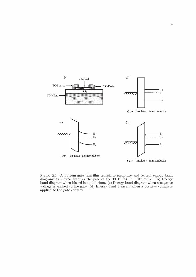
Figure 2.1 shows the basic layout of a bottom-gate thin-film transistor (TFT)
and energy band diagrams through the gate of an n-type accumulation-mode TFT
under three modes of operation. Figure 2.1b shows the equilibrium energy band
diagram, i.e., no bias is applied to the gate contact. As a negative bias is applied to
the gate, delocalized electrons in the channel are repelled from the semiconductor/gate
interface and create a depletion region, of positive charge, as indicated by the positive
curvature in the conduction and valence bands in Fig. 2.1c near the insulator. When a
positive voltage is applied to the gate contact, delocalized electrons in the channel are
attracted to the semiconductor/insulator interface, creating electron accumulation at
the interface, as indicated by the negative curvature in the conduction and valence
bands in Fig. 2.1d near the insulator.
The delocalized electrons that are accumulated near the semiconductor/insulator
interface when a positive voltage is applied to the gate contact provide a path for cur-
rent conduction, which is denoted as the channel. As a positive voltage is applied to
the drain contact of the TFT, these delocalized electrons in the accumulation layer
are extracted from the channel, giving rise to drain current through the TFT. At
small positive drain voltages, i.e., voltages significantly less than the gate voltage
minus the turn-on voltage, VDS << VGS - VON , the drain current conduction can
4
Glass
ITO/Gate
Channel
ITO/Source ITO/Drain
SiO2
Gate Insulator Semiconductor
EC
EF
EV
(a) (b)
Gate Insulator Semiconductor
EC
EF
EV
(c)
Gate Insulator Semiconductor
EC
EF
EV
(d)
Figure 2.1: A bottom-gate thin-film transistor structure and several energy banddiagrams as viewed through the gate of the TFT. (a) TFT structure. (b) Energyband diagram when biased in equilibrium. (c) Energy band diagram when a negativevoltage is applied to the gate. (d) Energy band diagram when a positive voltage isapplied to the gate contact.
5
be modeled as a linear relationship as is given by
IDS = (1/2)µCox(W/L)(2(VGS − VON )VDS − V 2DS), (2.1)
where the turn-on voltage (VON ) is the voltage at which current conduction begins
to increase with an increase in the gate voltage and is discussed in further detain in
Section 3.2.1[7], Cox is the oxide capacitance, µ is the mobility of the electrons, W is
the width of the channel, L is the length of the channel, VGS is the gate to source
voltage, and VDS is the drain to source voltage. When the drain voltage reaches the
pinch-off voltage, i.e., the voltage at which the channel near the drain is depleted of
carriers, the drain current saturates, thus becoming independent of the drain voltage,
and is given by
IDS = (1/2)µCox(W/L)((VGS − VON )2). (2.2)
Transistors are classified into two different types, based on whether drain cur-
rent flows through the TFT when no voltage is applied to the gate. If the TFT is
on, i.e., drain current flows through the TFT when no voltage is applied to the gate,
the TFT is distinguished as a depletion-mode device. If the TFT is off, i.e., only
leakage current flows through the TFT with no voltage applied to the gate, the TFT
is classified as an enhancement-mode TFT.
2.2 Inverter operation
An inverter is the simplest electronic circuit possible, consisting of a series
combination of a control transistor and a load, which is often another transistor.
An inverter is the most basic digital electronic circuit building block, allowing for
the creation of more complex logic. There are several different configurations for
inverters, as is detailed in Sedra and Smith. [13] Only one configuration involving an
enhancement-mode control and load transistor is discussed in this thesis.
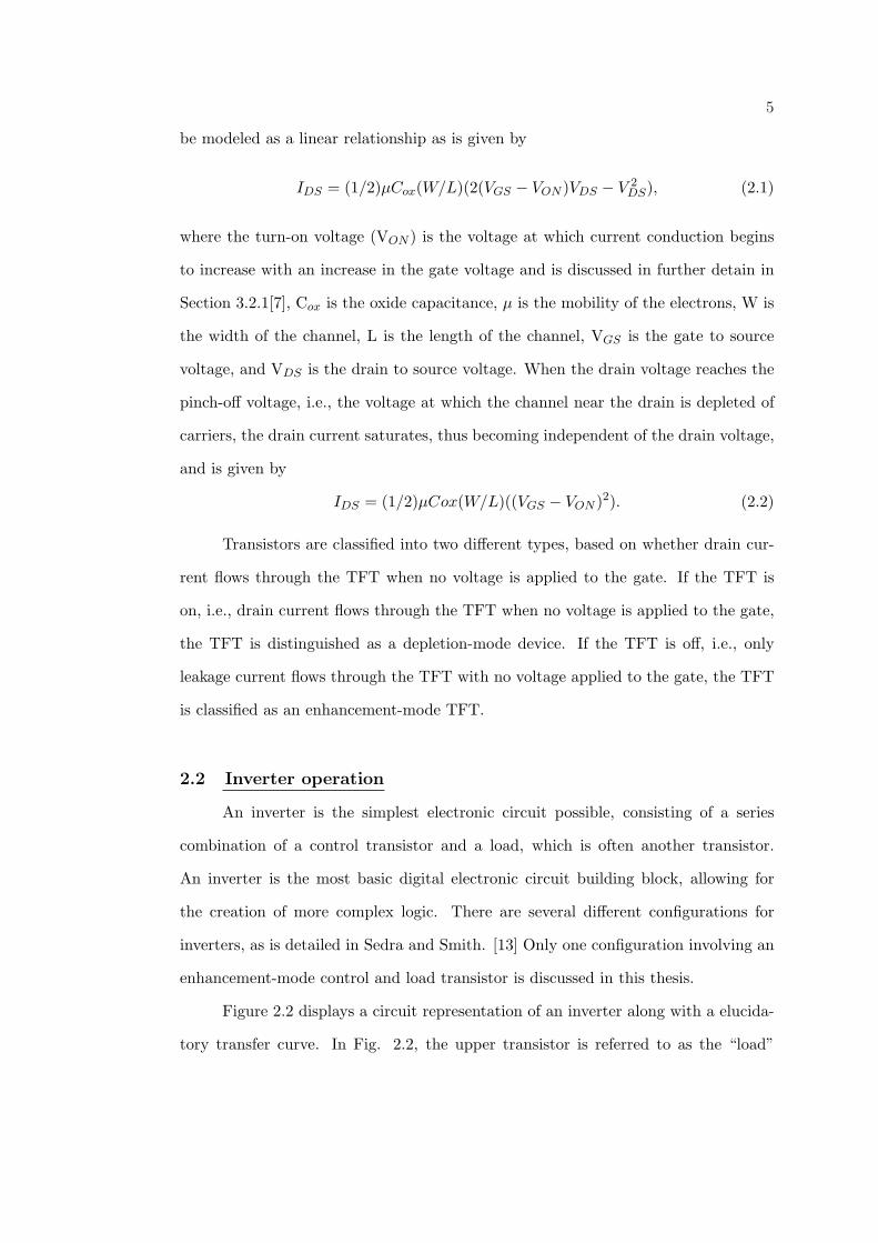
Figure 2.2 displays a circuit representation of an inverter along with a elucida-
tory transfer curve. In Fig. 2.2, the upper transistor is referred to as the “load”
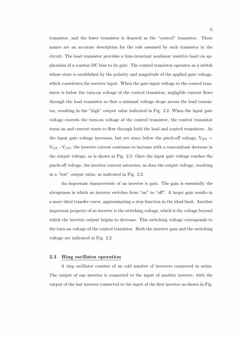
6
transistor, and the lower transistor is denoted as the “control” transistor. These
names are an accurate description for the role assumed by each transistor in the
circuit. The load transistor provides a time-invariant nonlinear resistive load via ap-
plication of a constat DC bias to its gate. The control transistor operates as a switch
whose state is established by the polarity and magnitude of the applied gate voltage,
which constitutes the inverter input. When the gate input voltage to the control tran-
sistor is below the turn-on voltage of the control transistor, negligible current flows
through the load transistor so that a minimal voltage drops across the load transis-
tor, resulting in the ”high” output value indicated in Fig. 2.2. When the input gate
voltage exceeds the turn-on voltage of the control transistor, the control transistor
turns on and current starts to flow through both the load and control transistors. As
the input gate voltage increases, but yet stays below the pinch-off voltage, VDS =
VGS - VON , the inverter current continues to increase with a concomitant decrease in
the output voltage, as is shown in Fig. 2.2. Once the input gate voltage reaches the
pinch-off voltage, the inverter current saturates, as does the output voltage, resulting
in a “low” output value, as indicated in Fig. 2.2.
An important characteristic of an inverter is gain. The gain is essentially the
abruptness in which an inverter switches from “on” to “off”. A larger gain results in
a more ideal transfer curve, approximating a step function in the ideal limit. Another
important property of an inverter is the switching voltage, which is the voltage beyond
which the inverter output begins to decrease. This switching voltage corresponds to
the turn-on voltage of the control transistor. Both the inverter gain and the switching
voltage are indicated in Fig. 2.2.
2.3 Ring oscillator operation
A ring oscillator consists of an odd number of inverters connected in series.
The output of one inverter is connected to the input of another inverter, with the
output of the last inverter connected to the input of the first inverter as shown in Fig.
7
Vout
Vin
high
low
dVout dVingain =
control
load
switchingvoltage
output
loadbias
input
Figure 2.2: A theoretical transfer curve and a circuit representation illustrating theessential features of the inverters employed in this thesis. Both the control andload transistors are n-channel, accumulation-mode TFTs, operating in enhancement-mode, i.e., possessing positive turn-on voltages.
8
Vdd
Vout
V1
I1
V2
I2
V3
I3
T1
T2
T3
T4
T5
T6
t=0V1 = 0I1 = small
t=τpV2 = highI2 = large
t=2τpV3 = lowI3 = small
Figure 2.3: Schematic representation of a ring oscillator showing the voltages andcurrents present at different times throughout device operation.
2.3. A ring oscillator is used to assess the speed of an integrated circuit technology.
The oscillation frequency of a ring oscillator is related to the switching speed of the
transistors comprising the ring oscillator. In turn, the switching speed of a transistor
is based on channel mobility, parasitic capacitances, and device dimensions.
A brief discussion of ring oscillator operation is presented here. For a more
thorough discussion see, Sedra and Smith [13]. The voltages and currents present in
a ring oscillator at various times are displayed in Fig. 2.3. At time t = 0, no voltage is
applied to the input of the first inverter, so that control transistor T1 is off. Since T1
is off, only a small amount of leakage current flows through this device. This small
leakage current also flows through the load transistor T2, resulting in a negligible
voltage drop across T2, thus producing a ”high” output of the first inverter. At time
9
t = τp, corresponding to one propagation delay or the time it takes for the output to
switch from low to high, a high voltage is applied to the input of the second inverter.
This high voltage turns on T3, thereby allowing current to flow through this second
inverter. This current produces a voltage drop across T4, resulting in a low output
voltage from the second inverter. At time t = 2τp, the input of the third inverter is
low yielding a high output voltage from the third inverter. This process continues
until the output of the fifth inverter, which is high, is applied to the input of the
first inverter at time t = 4τp. This process constitutes a voltage whose oscillation
continues as long as there are an odd number of inverters in series, and as long as the
gain for each inverter stage is greater than 1.
It should be noted that the oscillation frequency is equal to the inverse of 2nτp,
where n is the number of inverters in the ring oscillator. τp is determined by both
material properties and also by the device layout. Both the material properties and
device geometry need to be considered when comparing ring oscillator frequencies. A
large oscillation frequency does not necessarily mean superior device performance.
The material property that determines τp is mobility. Mobility is discussed
in further detail in Section 3.2.2. A higher mobility decreases the switching time,
thereby increasing the operating frequency.
The other important factor to consider when assessing oscillator frequency is
device layout. The oscillation frequency is significantly affected by parasitic capaci-
tances, which result from device layout. A large source-gate and/or drain-gate over-
lap increases the parasitic capacitance, thus decreasing the operating frequency of
the ring oscillator. The operating frequency is also effected by the device dimen-
sions, in particular, the width-to-length ratio of the control and load transistors. A
straightforward method to increase the operating frequency of a ring oscillator is to
decrease the channel length for the control and load transistors. As the channel length
decreases, the propagation delay of each inverter stage decreases, since electrons do
not have as far to travel across the channel, and the operating frequency increases.
10
Another factor that effects the ring oscillator operating frequency is the operating
voltage. As discussed in Section 3.2.2, mobility is dependant on the gate voltage
applied to the transistor, and increases as the gate voltage increases. Consequently a
higher operating voltage increases the ring oscillator operating frequency. Also, the
width-to-length ratio of the load and control transistor can be adjusted to increase
ring oscillator frequency. If the width of the load transistor is increased or the width
of the control transistor is decreased the ring oscillator oscillation frequency increases
but the voltage swing decreases. A sufficiently large voltage swing is required in or-
der to sustain oscillations, i.e., the output voltage of one inverter has to be able to
both turn-on and turn-off the control transistor of the following inverter, in order to
sustain oscillations.
In summary, when comparing different ring oscillator operating frequencies re-
ported in literature, it is important to recognize that all of these factors, i.e., transistor
dimensions (gate length and width-to-length ratio), parasitic capacitance (determined
by source/gate and gate/drain overlap capacitance), and operating voltage, be taken
into account in order to make an accurate comparison between different devices and
technologies.
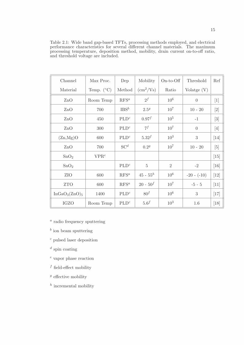
2.4 Previous reported TFTs based on wide band gap semiconductors
A significant amount of work has been reported with regard to wide band gap
semiconductors, both for use as transparent interconnects and also as TFTs. This
section summarizes only the work regarding wide band gap semiconductors for use as
TFTs, since this work is directly relevant to the research reported in this thesis. The
materials that are currently being investigated as channel materials include zinc oxide,
tin oxide, zinc indium oxide, zinc tin oxide, and indium gallium zinc oxide. Each of
these materials is briefly discussed in the following sections and is also summarized
in Table 2.1.
11
2.4.1 ZnO based thin-film transistors
Zinc oxide (ZnO) is currently the most commonly reported wide band gap semi-
conductor employed as a TTFT channel material. In 2003, Hoffman et al. fabricated
ZnO TTFTs by ion beam sputtering on glass substrates that had been coated with
indium tin oxide and a superlattice of aluminum oxide and titanium oxide [2]. The
channel material was deposited at near room temperature and then subjected to a
700 ◦C rapid thermal anneal in oxygen to increase the channel resistance. The highest
effective channel mobility achieved was 2.5 cm2V−1s−1. These devices had a thresh-
old voltage between 10 to 20 V, and an on-to-off ratio of 107. These TTFTs exhibited
little to no effect when exposed to light.
Also in 2003, Masuda et al. demonstrated ZnO TFTs in which the ZnO layer
was deposited by pulsed laser deposition (PLD). These devices used a double layer
gate insulator consisting of silicon dioxide and silicon nitride to reduce gate leakage
introduced by depositing ZnO directly onto the silicon dioxide. Masuda et al. found
that the Zn diffused into the silicon dioxide, thereby increasing the leakage current,
and that the introduction of a buffer layer of silicon nitride prevented Zn diffusion,
thus decreasing the leakage current. The best field effect mobility obtained was 0.97
cm2V−1s−1 with a threshold voltage of -1 V [3].
Additionally in 2003 Carcia et al. fabricated ZnO TFTs by rf magnetron sput-
tering on Si substrates in which the ZnO channel layer is deposited near room tem-
perature. Their best devices exhibit field-effect mobilities of more than 2 cm2V −1s−1
and an on-to-off ratio of 106[1].
In 2003, Nishii et al. fabricated ZnO TFTs using PLD [4]. These devices em-
ployed a CaHfOx buffer layer between the ZnO channel layer and the amorphous
silicon nitride gate dielectric to improve the channel mobility and decrease the pro-
cessing temperature required to achieve good device performance. These devices were
fabricated using conventional liquid crystal fabrication techniques, and mask layout.
By using the CaHfOx buffer layer the field effect mobility is increased to 7 cm2V−1s−1

12
when deposited at 300 ◦C and hysteresis was minimized. When no buffer layer was
used the films were too conductive, and possessed a large amount of hysteresis. The
ZnO deposition temperature could be reduced to 150 ◦C and no significant change in
device performance was observed.
In 2003, Norris et al. demonstrated a ZnO TTFT that had the channel layer
deposited via spin-coating [5]. The device employed a staggered, bottom-gate config-
uration, and used a superlattice of aluminum oxide and titanium oxide as the gate
dielectric. The channel was baked in air for 10 min at 600 ◦C to oxidize the chan-
nel, then rapid thermal annealed to 700 ◦C to improve crystallinity. The channel
and source/drain regions were patterned using photolithography. The devices had
an effective channel mobility of 0.2 cm2V−1s−1 and exhibited a higher sensitivity to
light when compared to ion-beam deposited channels. Norris et al. attributed this
increased light sensitivity to increased surface roughness.
In 2004, Kwon et al. fabricated TFTs using magnesium and phosphorous doped
ZnO as a channel layer. The magnesium is used to increase the band gap and the
phosphorous reduces the free carrier concentration. These TFTs were fabricated
using a top-gate configuration and used hafnium oxide as the gate dielectric. The
channel layer was deposited using PLD with a deposition temperature of 400 ◦C.
After deposition the channel layer was annealed to 600 ◦C in the presence of oxygen
to activate the phosphorous dopant and increase the resistance. The maximum field
effect mobility achieved was 5.32 cm2V−1s−1 [14].
2.4.2 Tin oxide based thin-film transistors
Even though ZnO is the most investigated wide band gap semiconductor for use
in TFTs, other materials have been investigated as well. The following summarizes
work related to tin oxide (SnO2), another wide band gap semiconductor of specific
relevance to this thesis.

13
In 1969, long before ZnO TFTs and TTFTs were investigated, Aoki et al. fab-
ricated a tin oxide (SnO2) TFT using a vapor phase reaction deposition methodology
[15]. The substrates were glazed alumina and used a dual layer silicon monoxide and
nitrocellulose gate dielectric. These TFTs operated as depletion-mode gate-controlled
resistors, which could not be turned off and did not exhibit current saturation but
which possessed a transconductance of 0.3 mmho. Since these devices could not be
turned off and did not exhibit drain current saturation, they cannot really be consid-
ered to function as true TFTs.
In 1996 almost 30 years after Aoki et al. demonstrated their SnO2 TFT, Prins
et al. fabricated a SnO2 TFT using PLD of the SnO2 channel onto a SrTiO3 substrate
[16]. The gate dielectric was PbZr0.2Ti0.8O3, a ferroelectric material which allows
the TFT to possess a memory. The TFT has a mobility of 5 cm2V−1s−1 and an
on-to-off ratio of 2. The TFT fabricated was a depletion-mode device. The voltage
shift between the positive sweep and the negative sweep was 1.6 V.
2.4.3 Indium gallium zinc oxide thin-film transistors
Another wide band gap semiconductor that has been reported as being used as
a channel material in TTFTs is indium galium zinc oxide (InGaO3(ZnO)5). In 2003,
Nomura et al. fabricated a TTFT using a single crystal superlattice of InGaO3(ZnO)5
by using a reactive solid-phase epitaxy process to deposit the epitaxial channel layer
[17]. These devices employed a hafnium oxide gate insulator on a single-crystal yttri-
astabilized zirconia substrate. InGaO3(ZnO)5 TTFTs exhibited a threshold voltage,
on-to-off ratio, and field-effect mobility of 3 V, 106, and 80 cm2V−1s−1, respectively.
This is the highest reported mobility for a TTFT.
In 2004, Nomura et al. demonstrated a flexible TTFT using an amorphous
indium gallium zinc oxide channel material, deposited by PLD onto a polyethylene
terephthalate substrate [18]. The devices utilized a yitrium oxide gate insulator. The
devices were fabricated at room temperature, and exhibited a saturation mobility and
14
on-to-off ratio of 6-9 cm2V−1s−1, 103 respectively. Only a small decrease in saturation
mobility was observed while the substrate was flexed.
2.4.4 Zinc tin oxide thin-film transistors
In 2005, Chiang et al. fabricated a TTFT using zinc tin oxide (ZTO), an
amorphous wide band gap semiconductor, as the channel layer [11]. The ZTO was
deposited using radio frequency magnetron sputtering. These devices utilized an
ATO gate insulator, and exhibited a field-effect mobility of 5-15 cm2V−1s−1 and 20-
50 cm2V−1s−1 when annealed at 300 ◦C and 600 ◦C, respectively. ZTO TFTs have
a turn-on voltage between -5 and 5 V, and have an on-to-off ratio greater than 107.
2.4.5 Thin-film transistors fabricated using zinc indium oxide
Another wide band gap semiconductor that has been reported as being used as
a channel material in TTFTs is zinc indium oxide (ZIO). Dehuff et al. demonstrated
a TTFT using amorphous ZIO as the channel material in 2005 [12]. The ZIO chan-
nel was deposited using radio frequency magnetron sputtering. Both depletion- and
enhancement-mode TTFTs were demonstrated. The TTFTs utilized an ITO-coated
glass substrate, and a superlattice of ATO as the gate insulator. These TTFTs ex-
hibited a large incremental mobility of 10 - 30 cm2V−1s−1, and 45 - 55 cm2V−1s−1
for enhancement- and depletion-mode devices, respectively. Dehuff et al. also re-
ported the fabrication of ZIO TTFTs at room temperature. These TTFTs were
enhancement-mode and had an incremental mobility of 8 cm2V−1s−1.
2.5 Tin oxide material properties and conventional applications
There are two forms of tin oxide, differing by the electronic state of the tin
atom. When the tin atom is in the 4+ oxidation state, the tin oxide that is formed is
stannic oxide (SnO2) [19]. When the tin atom is in the 2+ oxidation state, stannous
oxide (SnO) is formed [19]. Stannic tin oxide is a wide band gap semiconductor with
15
Table 2.1: Wide band gap-based TFTs, processing methods employed, and electricalperformance characteristics for several different channel materials. The maximumprocessing temperature, deposition method, mobility, drain current on-to-off ratio,and threshold voltage are included.
Channel Max Proc. Dep Mobility On-to-Off Threshold Ref
Material Temp. (◦C) Method (cm2/Vs) Ratio Volatge (V)
ZnO Room Temp RFSa 2f 106 0 [1]
ZnO 700 IBSb 2.5g 107 10 - 20 [2]
ZnO 450 PLDc 0.97f 105 -1 [3]
ZnO 300 PLDc 7f 107 0 [4]
(Zn,Mg)O 600 PLDc 5.32f 103 3 [14]
ZnO 700 SCd 0.2g 107 10 - 20 [5]
SnO2 VPRe [15]
SnO2 PLDc 5 2 -2 [16]
ZIO 600 RFSa 45 - 55h 106 -20 - (-10) [12]
ZTO 600 RFSa 20 - 50f 107 -5 - 5 [11]
InGaO3(ZnO)5 1400 PLDc 80f 106 3 [17]
IGZO Room Temp PLDc 5.6f 103 1.6 [18]
a radio frequency sputtering
b ion beam sputtering
c pulsed laser deposition
d spin coating
e vapor phase reaction
f field-effect mobility
g effective mobility
h incremental mobility

16
a band gap of 3.6 eV [19], whereas stannous tin oxide has a band gap of 2.5 - 3
eV. Stannic tin oxide has the rutile crystal structure, and starts to crystalize at 350
◦C, while the stannous form of tin oxide has the litharge structure. Stannic is the
most common form of tin oxide and is the only form that is useful in gas sensing
applications. The density of tin oxide is 6.99 g cm−3 [19]. Undoped, stoichiometric
SnO2 is an insulator, however, oxygen vacancies render it n-type. The formation
energy of oxygen vacancies and tin intersticials is very low, so it is hard to deposit a
stoichiometric film, and most films turn out to be conductive [19].
There are three major uses of tin oxide, gas sensors, transparent interconnects,
and window coatings. These applications are discussed in the following sections.
2.5.1 Tin oxide as a transparent interconnect
The most common transparent interconnect used today is indium tin oxide
(ITO). Since indium is a rare metal and is quite expensive, a significant amount of
research effort is being devoted towards the development of an alternative material
to be used as a transparent interconnect. The most popular oxides that are being
explored are zinc oxide and tin oxide. This section briefly describes techniques used
to make tin oxide conductive for use as a transparent interconnect.
Tin oxide is one of the materials being focused on as a alternative to ITO.
The most common approaches to make tin oxide conductive is by doping with an-
timony as a cation dopant or fluorine as an anion dopant [19]. Even with these
dopants the conductivity of SnO2 is still lower than that of doped ZnO and ITO.
Performance, process integration considerations, and cost normally determine which
of these transparent conducting oxides are used. ITO has the highest conductivity of
the transparent conductive oxides, but the limited amount of indium in the earth’s
crust is driving up the cost. ZnO has a higher conductivity than that of SnO2, but
ZnO is not very physically or chemically robust and can be etched very easily, so

17
process integration of ZnO can be challenging. In contrast, SnO2 is chemically and
physically robust.
2.5.2 Tin oxide as a gas sensor
There are two types of gas sensing materials, surface sensing and bulk sensing
[19]. In bulk sensing materials, their conductivity increases as a consequence of gas
exposure due to the creation of bulk vacancies. An example of a bulk sensing material
is titanium oxide [19]. Tin oxide is an example of a surface sensing material in which
the surface conductivity is increased by reduction of the tin on the surface upon as
exposure and the bulk of the material is unaffected by the presence of the gas. If the
gas to be detected is an oxidizing gas the conductivity decreases upon gas exposure
due to the formation of a depletion layer at the surface [19].
Tin oxide gas sensors are typically passive components. The tin oxide is inten-
tionally doped to make it conductive. The type of dopant used can effect the sensors
sensitivity to certain gases [19]. The conductivity of the SnO2 is measured as the
sensor is exposed to the gas. The tin oxide surface, when it is exposed to normal air
atmosphere, adsorbs a layer of negatively charged O2 atoms, leading to the creation
of a depletion region at the surface and a corresponding decrease in the conductivity.
When a reducing gas is then introduced, negatively charged surface oxygen atoms
react with the gas and are replaced by other molecules which results in a decrease in
the depletion layer and an increase in the conductivity [19].
2.5.3 Tin oxide as a window coating
Certain wide band gap oxide semiconductors have another useful characteristic.
Since they have a wide band gap, the visible portion of the electromagnetic spectrum
can pass through, but the infrared part is reflected. This is a useful property for win-
dow coating applications. Visible light is passed, but the infrared light, i.e., radiant
heat is reflected, based on the plasma frequency of the material. The plasma fre-
18
quency is the frequency above which an electromagnetic wave is not be able to travel
through a material. This phenomena is related to the frequency dependance of the
dielectric constant of the material [20]. The dielectric constant of a material is a mea-
sure of the ability of a material to respond to an applied electric field. The frequency
dependance of the dielectric constant of a material depends on the relaxation time of
the material. At a given frequency, if the dielectric constant is positive, the electro-
magnetic wave is able to propagate through the material. However if the dielectric
constant is negative, the electromagnetic wave cannot propagate in the material, but
decays exponentially inside the material such that the incident wave is reflected from
the material’s surface [20]. The plasma frequency of a material is expressed as,
ωp ≡ ((4πne2)/m)1/2, (2.3)
where n is the free electron density of the material and m is the mass of an electron
[20]. The wavelength associated with the plasma frequency is given by,
λp ≡ (2πc)/ωp, (2.4)
where c is the speed of light [20]. From Eqn. 2.3 it is eviden that the plasma frequency
depends on the doping concentration of the material. A higher carrier concentration
leads to a larger plasma frequency, which translates into a smaller critical wavelength
at which electromagnetic radiation is reflected at the material’s surface. Therefore the
infrared transmission characteristics of a window can be tailored to a specific climate
by changing the carrier concentration of the transparent coating deposited onto the
window’s surface. Tin oxide is the most widely used transparent semiconductor for
this application due to its low cost, compared to ITO, and its chemically robust
nature, compared to ZnO.
2.6 Pentacene organic ring oscillators
A significant amount of research has been devoted to the realization of ring
oscillators using organic filed-effect transistors (OFETs). The most common channel

19
material used in OFETs and OFET ring oscillators is pentacene. This section sum-
marizes published literature related to pentacene OFET ring oscillators and thereby
serves as a comparison to the inorganic TTFT ring oscillators presented in this the-
sis. Table 2.2 summarizes the results of published ring oscillators fabricated using
pentacene as an active channel material.
In 1999, Klauk et al. demonstrated a pentacene ring oscillator on a glass sub-
strate using ion beam sputtered silicon dioxide as the gate insulator [21]. The pen-
tacene OFETs have a field-effect mobility of 0.5 cm2V−1s−1, and an on-to-off ratio
of 107. The pentacene OFETs are depletion-mode. Therefore, a level-shifting circuit
is required to fabricate a ring oscillator. The control transistor has a channel length
of 5 µm and a width of 800 µm, when the load transistor had a channel length of 30
µm and a width of 300 µm. The pentacene ring oscillators with level-shifting have a
minimum propagation delay of 73 µs. This propagation delay is limited by the use of
the level-shifting circuit, and not by the performance of the pentacene OFETs.
In 2000, Gelinck et al. reported pentacene OFET seven-stage ring oscillators
that have a frequency of 2 kHz at a supply voltage of less than 5 V, with a channel
length of 1 µm [22]. When the channel length is increased to 5 µm the frequency
drops to 60 Hz. These devices were fabricated using a bottom-gate design, and
deposited onto a glass substrate. The pentacene OFETs exhibited a mobility of 10−2
cm2V−1s−1. After being exposed to air for one month the pentacene OFETs only
showed a small degradation in performance.
Also in 2000, Kane et al. demonstrated a five-stage OFET ring oscillator on a
polyester substrate using pentacene as the active channel layer [23]. When biased at
20 V, these ring oscillators operated at a frequency of 1.7 kHz, which translates into
a propagation delay of 52 µs per stage. The pentacene OFETs had a mobility of 0.45
cm2V−1s−1, and a threshold voltage of 3.2 V. Due to the positive threshold voltage of
these p-channel pentacene OFETs, level-shifting circuits were incorporated into the
ring oscillator design. The OFETs used to fabricate the five-stage ring oscillator had
20
a channel length of 10 µm. Kane et al. claim that a propagation delay of 52 µs is the
shortest delay reported on plastic substrates.
In 2000, Sheraw et al. reported pentacene OFET five-stage ring oscillators with
a propagation delay as low as 40 µs on flexible substrates [24]. The pentacene OFETs
exhibited a mobility of 0.4 cm2V−1s−1, threshold voltage of 0.9 V and an on-to-off
ratio of 107. With the positive threshold voltage of these p-channel pentacene OFETs,
the ring oscillators had to employ level-shifting circuitry. Sheraw et al. also report
that the ring oscillators had a propagation delay of under 50 µs when biased at 8
V. These are very low propagation delays for pentacene circuits processed on flexible
substrates. However, device dimensions were not specified for the ring oscillator
circuit, so a direct comparison to other reports cannot be made. The propagation
delay of a ring oscillator circuit is strongly based on the circuit layout and device
geometries.
Zschieschang et al. demonstrated pentacene OFET ring oscillators on flexible
substrates using a printed gate electrode in 2003 [25]. The pentacene OFETs had
a saturation mobility of 0.06 cm2V−1s−1, a threshold voltage of 1 V, and an on-to-
off ratio of 106. The ring oscillators were fabricated using pentacene OFETs with
a channel length of 5 µm, channel width of 20 µm, and a contact overlap of 5 µm.
The ring oscillators implemented a level-shifting circuit to accommodate the positive
threshold voltage of the pentacene OFETs. The five-stage ring oscillators fabricated
using a printed gate electrode had a propagation delay of 200 - 300 µs.
In 2004, Eder el al. demonstrated five-stage ring oscillators using both a paper
substrate and a flexible polyetherether ketone film substrate. These five-stage ring
oscillators used an organic pentacene channel layer [26]. The pentacene layer was
deposited using thermal evaporation, and had a saturation mobility of 0.3 cm2V−1s−1
and an on-to-off ratio of 106 when deposited onto a polyetherether ketone film. The
OFET circuits fabricated on polyetherether ketone film employed a 5 µm channel
length and had a contact overlap of 5 µ, and had an oscillation frequency of 4.5 kHz,
21
Table 2.2: A summary of pentacene-based ring oscillator device geometry and per-formance. The mobility, channel length, channel width, contact overlap, use of level-shifting circuitry, and propagation delay are included.
Mobility Channel Channel Contact delay Level- Ref
(cm2/Vs) Length(µm) Width(µm) Overlap(µm) (µs) shifting
0.5a 5 800 - 73 yes [21]
10−2a 1 - - 36 yes [22]
0.45a 10 - - 59 yes [23]
0.4a - - - 37 yes [24]
0.06b 5 20 5 200 - 300 yes [25]
0.2b 5 - 5 22 yes [26]
a field-effect mobility
b saturation mobility
which translates into a propagation delay of 22 µseconds. Due to surface roughness
the ring oscillators fabricated on a paper substrate had a channel length of 10 µm, and
had a contact overlap of 10 µm. These ring oscillators had an oscillation frequency
of 8 Hz, which is equivalent to a propagation delay of 12 milliseconds. All of these
circuits employ level shifting due to the positive turn-on voltage of the p-channel
pentacene OFETs.
2.7 Conclusions
In this chapter basic operation of several different devices and circuits is pre-
sented, including thin-film transistors, inverters, and ring oscillators. A brief review
of the literature pertaining to transparent electronics is presented. The material
properties and conventional applications for tin oxide are discussed. Finally, a brief

22
review of pentacene ring oscillator literature is offered as a basis of comparison to the
transparent ring oscillators presented in this thesis.
23
3. EXPERIMENTAL TECHNIQUE
In this chapter the deposition techniques used to fabricate the devices presented
in this thesis are discussed. Also device and integrated circuit figures-of-merit are
presented and discussed.
3.1 Thin film deposition techniques
This section contains information on the methods and tools used in the depo-
sition of the semiconductor materials utilized in this work. These methods include
physical vapor deposition, chemical vapor deposition, and photolithography.
3.1.1 Physical vapor deposition techniques
A brief discussion of different physical vapor deposition (PVD) methods used
for this work is presented. The PVD methods discussed include evaporation, radio
frequency magnetron (RF), and direct current (DC) sputtering.
3.1.1.1 Thermal evaporation
Thermal evaporation is a PVD method used to deposit materials with relatively
low melting points. Evaporation is performed under high vacuum ≤ 5 × 10⁻⁶ Torr.
Evaporation of the material takes place as current is passed through a filament, or a
boat, containing the material to be evaporated. As current flows through the boat the
boat heats up, due to resistive heating, until the material either melts and evaporates
or sublimes, i.e., changes directly from a solid to a vapor.
The evaporation system used in this work is a VECO Thermal Evaporator. The
system has three evaporation sources, which allows for deposition of multiple materials
without breaking vacuum. This allows for higher efficiency and less contamination
of the deposited films. Evaporation is an alternative method investigated for the
deposition of SnO2 and indium in this work.

24
3.1.1.2 Activated reactive evaporation
Activated reactive evaporation (ARE) is another form of thermal evaporation.
ARE also uses resistive heating to evaporate the source material. The only difference
is that ARE uses a plasma source to ionize gas ions that reacts with the evaporated
material. An example of a material deposited using ARE is titanium oxide. Titanium
metal is evaporated and oxygen is ionized and reacts with the evaporated Ti, resulting
in titanium oxide.
ARE is investigated as an alternative method for depositing tin oxide. Tin
metal is evaporated in the presence of activated O2 ions to produce SnO2 films.
The ARE system at OSU has two thermal sources, and uses an electron cyclotron
resonance (ECR) source to ionize the reactive gas.
3.1.1.3 Radio frequency sputtering
RF sputtering uses a radio frequency power supply, operating at 13.56 MHz, to
generate a plasma, which creates ions which are used to sputter the target material.
The ions are accelerated towards the target by a negative DC bias on the target
due to the flux of electrons. The ions hit the target with enough energy to dislodge
the target atoms, which are then redeposited onto the substrate. RF sputtering is
performed under vacuum, typically between 1 mTorr and 50 mTorr, to improve the
quality and the deposition rate of the deposited film. A lower pressure increases the
mean free path, the distance between collisions, and results in the deposited species
having more energy to diffse along the substrate surface in order to find the lowest
energy state possible. A more thorough discussion of plasmas and sputtering can be
found in Lieberman. [27]
RF sputtering can be used to sputter both insulating and conducting targets,
since charge does not build up on the surface of the target. The major disadvan-
tages of RF sputtering are cost and deposition rate. A RF power supply is more
expensive than an equivalent DC power supply, and the deposition rate is lower than
25
that obtained using DC sputtering, as a result of the alternating nature of the RF
waveform.
3.1.1.4 Direct current sputtering
The only major change from RF to direct current (DC) sputtering is the power
supply used. In DC sputtering, as the name suggests, a DC power supply is used
to create the plasma. The physics of the sputtering process is unchanged. Direct
current sputtering allows for higher deposition rates and is less expensive than RF
sputtering.
Conventional DC sputtering can only be used to sputter conductive targets.
The flux of electrons from the DC supply causes charge to build-up on the surface of
an insulating target, rendering the plasma unstable so that it eventually extinguishes.
One method used to sputter insulating targets using DC sputtering involves the use
of a pulsed DC source. When using a pulsed DC source, the voltage is periodically
pulsed positive for a very short time to remove the charge on the insulating target.
This positive pulse duration is a very small fraction of the entire period, resulting in
a higher sputter rate than that of RF sputtering.
Another method utilized to allow DC sputtering of insulating targets is a sec-
ondary ion beam sputtering system. In this configuration, the plasma is generated
in a chamber separate from that of the substrate. The ions are extracted from the
plasma chamber and are accelerated towards the target. A neutralizer is used in this
configuration to neutralize the ions, which eliminates the build up of charge on the
surface of an insulating target. Therefore this configuration allows for sputtering of
insulating targets, and is the configuration of the DC sputtering system used in this
work.
3.1.2 Chemical vapor deposition techniques
Unlike PVD, chemical vapor deposition (CVD) relies on a chemical reaction
to deposit the film rather than a physical process. In CVD, multiple reactive gases
26
are combined and the reaction takes place at the heated substrate, resulting in the
deposition of the film. There are many different types of CVD reactors including,
atmospheric, low-pressure, and plasma-enhanced (PECVD). During this work only a
PECVD system is used and is the only type of reactor discussed in this thesis.
3.1.2.1 Plasma-enhanced chemical vapor deposition
In a PECVD system a plasma provides some of the activation energy required
for the chemical reaction, in effect reducing the processing temperature required dur-
ing the film deposition. PECVD systems allow for high deposition rates and the
ability to deposit films on substrates with lower thermal stability than with other
CVD systems.[28]
Silicon dioxide (SiO2) deposited in a PECVD system is used as a gate insulator
for the transparent circuits presented in this thesis. The PECVD system at Oregon
State University is a Semi Group PECVD system and uses silane and nitrous oxide
as precursors. The chemical reaction to create silicon dioxide using these precursors
is
SiH4(gas) + 2N2O(gas)200−400◦C,rf−−−−−−−−−→ SiO2(solid) + 2N2(gas) + 2H2(gas). (3.1)
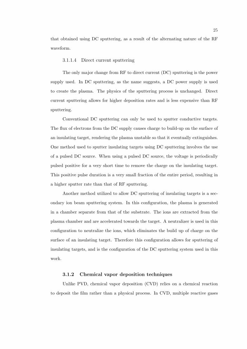
The Semi Group PECVD system is a cold-wall reactor, the configuration of which is
shown in Fig. 3.1. In a cold-wall reactor the chamber is actively cooled to reduce film
formation on chamber walls, reducing a source of contamination. The PECVD system
used for this research has been modified with an additional lamp heater to reduce
particulate contamination, arising from poorly adhered films on the gas diffuser plate
flaking off and being incorporated in the growing film. A detailed operating and
maintenance procedure for the Semi Group PECVD system is presented in Appendix
A.
27
Vacuum Pump
heater/bottom electrode
cooling water inlet cooling water inlet
Gas and RF inlet
gas diffuser plate/ top electrode
Figure 3.1: Schematic drawing showing a parallel plate cold-wall plasma-enhancedchemical vapor deposition system. This configuration is used to deposit silicon dioxideused as a gate insulator in the transparent circuits.
3.1.3 Etching processes
Etching is the process of removing material from a substrate. There are two
major qualities that distinguish an etch process. These qualities are etch profile and
selectivity. Etch profile refers to the topography of the etched film’s surface, and is
either isotropic or anisotropic. Isotropic etches remove the material in all directions
at an equal rate. Anisotropic etches are directional etches; they remove the film in
one direction much faster than in the other directions. Selectivity refers to how fast
an etch process etches one film compared to the etch rate of a different film. There are
three different types of etch processes discussed in the following sections, including
chemical etch, physical etch, or a combination of both chemical and physical etches.
3.1.3.1 Chemical etch
Often a chemical etch is referred to as a wet etch, since most chemical etches
require the substrate to be exposed to a liquid etchant. Wet etches have a higher se-

28
lectivity than physical etches, with the ability to remove one film off of an existing film
without damaging the bottom film. Chemical etches are commonly used to pattern
devices with larger dimensions, since etch chemistries typically are well understood
and greater selectivity can be achieved compared to physical etches. Wet etches are
isotropic, which limits the minimum device dimensions that can be patterned. [28]
Chemical etches are used to pattern gate contacts and channel layers in the
transparent circuits described in Chapter 5. Both the gate contacts and the channel
are etched using hydrochloric (HCl) acid. The gate contacts are etched using undi-
luted HCl, 37.5% HCl. When etching the channel layer, HCl is diluted with deionized
water at a ratio of five parts deionized water to one part HCl.
3.1.3.2 Physical etch
A physical etch, or dry etch as it is often called, uses a physical ion bombard-
ment, i.e., sputtering, to remove unwanted material. A physical etch is an anisotropic
etch, since the etch is directed in one direction. One disadvantage of a physical etch
is poor selectivity. An example of a physical etching system is an ion beam etcher.
An ion beam etcher uses a focussed beam of ions, as the name suggests, to sputter
away unwanted material. No physical etches are used in this work, but the concept
is presented to better understand the reactive ion etching process, which is used in
this work.
3.1.3.3 Reactive ion etch
Reactive ion etch (RIE) uses both a chemical and a physical process to remove
unwanted material. In a RIE process, a reactive gas is introduced into the chamber
and a glow discharge is created. The reactive gas reacts with the film and the ions
created in the glow discharge are directed towards the substrate, weakening bonds
and creating a more anisotropic etch. A RIE is used to etch the silicon dioxide gate
dielectric in transparent circuits.

29
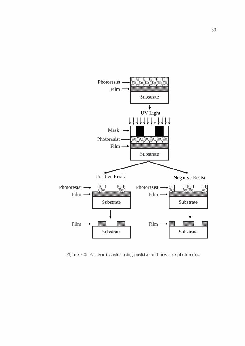
3.1.4 Photolithography techniques
Photolithography is used in semiconductor processing to pattern films down
to less than one micron. Photolithography involves transferring an image from a
mask to the photoresist, an organic polymer which becomes soluble when exposed to
ultraviolet light. The transparent circuits presented in this thesis are patterned using
photolithography.
3.1.4.1 Types of photoresist
There are two types of photoresist which differ from each other by the resulting
pattern after development. A positive resist transfers an exact copy of the mask to
the film, in other words what is exposed is removed in the developer. A negative
photoresist transfers an inverted mask pattern to the film, or what is not exposed is
removed while being developed. Figure 3.2 shows the pattern transfer for the different
photoresist types.
3.1.4.2 Exposure and development
Once the photoresist is spun onto the substrate, the pattern needs to be trans-
ferred into the resist. This is accomplished by exposure and development. Exposure
refers to when the photoresist is placed under an ultraviolet light source. For a posi-
tive photoresist, the bonds in the exposed area are weakened. When using a negative
resist, the bonds in the exposed area are cross-linked and become stronger. After the
photoresist is exposed, the substrate is submersed in a developer bath. The developer
removes the photoresist with the weaker bonds and leaves behind the desired pattern.
3.1.4.3 Film patterning
The two methods used in this work to pattern thin films are etching and lift-off.
Etching is the preferred process since the photoresist is spun on after the film has
been deposited, which does not affect any of the deposition parameters. There is
also no chance of contaminating the interface between the two films when etching is
30
Photoresist
Film
Substrate
Photoresist
Film
Substrate
Mask
UV Light
Photoresist
Film
Substrate
Photoresist
Film
Substrate
Positive Resist Negative Resist
Film
Substrate
Film
Substrate
Figure 3.2: Pattern transfer using positive and negative photoresist.

31
employed. Lift-off is a technique used to remove unwanted material that cannot be
etched. This technique requires pattering of the photoresist prior to the deposition of
the film. After the film is deposited, the photoresist and unwanted film are removed
by submersing the substrate in an acetone bath. After a long soak, the substrate is
placed in an ultrasonic cleaner to help remove any remaining unwanted film. Lift-
off has several disadvantages and is only used when etching is not feasible. One of
these disadvantages is that the photoresist is on the substrate while the film is being
deposited, which limits the deposition temperature. Another disadvantage of using
lift-off is the possible contamination of the interface between the two films, since the
photoresist is spun on before depositing the film.
3.2 Electrical characterization
Electrical characterization is used to evaluate the performance of devices. The
main figures-of-merit used to characterize a TTFT are turn-on voltage, mobility, and
drain current on-to-off ratio. The main figure-of-merit used to characterize a ring
oscillator is operating frequency. These figures-of-merit are discussed in the following
sections.
3.2.1 Turn-on voltage
Turn-on voltage (VON ) is the voltage at which current conduction begins to
increase with an increase in the gate voltage. [7] VON is determined by plotting
log(ID) versus VGS and finding the voltage at which the drain current starts to
increase from the leakage current/noise floor, as indicated in Fig. 3.3. A n-type
device that has a positive turn-on voltage is distinguished as enhancement-mode and
requires a gate voltage to be applied before drain conduction begins. When a n-type
device has a negative turn-on voltage, it is identified as depletion-mode and requires
a negative voltage to be applied to the gate to turn off the device.

32
-10 0 10 20 30 40
VGS(V)
-14
-12
-10
-8
-6
-4
-2
Lo
g(I
D)
-14
-12
-10
-8
-6
-4
-2
Lo
g(I
G)
VON
Leakae current/noise floor
Figure 3.3: Log(ID) versus VGS plot for an IGO TFT indicating the turn-on voltage,and leakage current/noise floor.
3.2.2 Mobility
Mobility is a measurement of how fast carriers can move through a material. A
higher mobility allows for a faster switching time, i.e., the time it takes for the device
to toggle between the off state and on state. In the off state, a minimal amount of
current flows through the device. In the on state, a significant amount of current
flows. A larger mobility value means that the device can conduct more current.
Three different mobilities used to characterize a device are incremental, average, and
saturation mobility. [7] These mobilities are discussed briefly in the following sections.
A more thorough discussion can be found in Hoffman’s article. [7]
3.2.2.1 Incremental mobility
The incremental mobility is the mobility of differentially induced carriers intro-
duced into the channel by a small increase in the gate voltage. [7] The incremental
33
mobility is calculated as [7]
µINC(VGS) =G′
D(VGS)WL CI
∣∣∣∣∣VDS→0
, (3.2)
where G′D(VGS) is the change in channel conductance with a change in gate voltage
as
G′D(VGS) =
∂GD(VGS)∂VGS
,
∣∣∣∣∣VDS→0
, (3.3)
where the channel conductance as a function of gate bias is given by [7]
GD(VGS) =ID
VDS
∣∣∣∣∣VDS→0
, (3.4)
and where CI is the capacitance of the insulator, W and L are the width and length
of the device, respectively, and∣∣∣VDS→0 indicates the device is biased in the linear
regime of transistor operation.
3.2.2.2 Average mobility
The average mobility is the average of all the carriers present in the channel
and can be calculated as [7]
µAV G(VGS) =GD(VGS)
WL CI(VGS − VON )
∣∣∣∣∣VDS→0
. (3.5)
3.2.2.3 Saturation mobility
The saturation mobility is the least used type of mobility. It is extracted from
an ID-VGS curve when the device is biased in saturation.[29] The saturation mobility
is calculated as [29]
µSAT =2m2
WL CI
∣∣∣∣∣saturation
, (3.6)
where m is the slope of the IDS versus VGS curve.
3.2.3 Drain current on-to-off ratio
The drain current on-to-off ratio is an indicator of how well a device will work
as a switch. The drain current on-to-off ratio is obtained by plotting the log(ID)
34
versus VGS at a large VDS . A large drain current on-to-off ratio is required for
certain switching applications, typically larger than 106 is preferred. The off current
translates into how much power is lost when the device is off, whereas the on current
indicates the maximum current drive for the device.
3.2.4 Operating frequency
The operating frequency refers to the frequency of oscillation of a ring oscillator
and is determined by the device physics, properties of the transistor, and the circuit
layout. The operating frequency for a ring oscillator can be obtained as
f =1T
=1
N2td, (3.7)
where N is the number of stages in the ring oscillator, and td is the propagation delay
for a single stage. SPICE simulation is an easy way to obtain an estimate of the
propagation delay, as demonstrated in Fig. 3.4. The propagation delay for each stage
is the sum of the rise time and the fall time of the output curve. The rise time and
fall time is the amount of time between the input voltage switching and the switching
voltage, when the output voltage reaches half of the maximum output voltage, as
indicated in Fig. 3.4.
3.3 Conclusions
In this chapter the deposition techniques used to fabricate the devices presented
in this thesis are discussed. These deposition techniques include physical and chemical
vapor deposition, as well as photolithography. A brief discussion of mobility, turn-on
voltage, on-to-off ratio, and operating frequency is presented.

35
trtf
-1.0
4.0
9.0
14.0
19.0
24.0
29.0
34.0
Vo
lta
ge
(V)
0.0 5.0E-6 1.0E-5 1.5E-5 2.0E-5 2.5E-5 3.0E-5
Time (sec)
3.5E-5 4.0E-5
Figure 3.4: SPICE simulation output for an inverter stage, indicating how rise andfall times are measured. The solid line is the output voltage from the inverter. Thedashed trace is the input voltage to the inverter stage, and the gray solid line indicatesthe switching voltage for the inverter stage.
36
4. TIN OXIDE TRANSPARENT THIN-FILM TRANSISTORS
This chapter is devoted to a discussion of the fabrication and characterization
of SnO2 TTFTs.
4.1 SnO2 TTFT device fabrication
Bottom-gate SnO2 TTFTs are fabricated on glass substrates, manufactured by
Nippon Sheet Glass Company, coated with 200 nm sputtered indium tin oxide (ITO)
and a 220 nm atomic layer deposited superlattice of Al2O3 and TiO2 (ATO) provided
by Planar Systems, Inc. The ITO and ATO layers constitute the gate contact and
insulator, respectively. Typically, the channel layer is deposited by RF magnetron
sputtering using a tin oxide target (Cerac) in Ar/O2 (97%/3%) at a pressure of 5
mTorr, power density of ∼3 W cm−2, target-to-substrate distance of ∼7.5 cm, and
no intentional substrate heating. The channel layers are typically 10-20 nm thick.
The channel length and width are 1524 µm and 7620 µm, respectively. Alternatively,
SnO2 channel layers are formed either by thermal evaporation at a pressure of ∼10−6
Torr or by activated reactive evaporation in either microwave-activated O2 or N2 at
a pressure of ∼ 5×10⁻⁴ Torr. In both cases, SnO2 powder is used as the evaporation
source material. After deposition of the SnO2 channel layer the sample is annealed,
typically via furnace or rapid thermal annealing (RTA) in O2 at 600 ◦C. Finally, ITO
source and drain contacts are formed by ion-beam sputtering.
4.2 SnO2 TTFT electrical characteristics and discussion
Figure 4.1 displays the DC drain current-drain voltage (IDS-VDS) character-
istics for a SnO2 TTFT. The slopes of most of the IDS curves shown in Fig. 4.1
are extremely flat at large VDS , indicating that a condition of ’hard saturation’ is
achieved, due to complete pinch-off of the channel. However, the two uppermost IDS
curves exhibit a small slope since the condition for pinch-off, i.e., VDS ≥ VGS - VT

37
0 10 15 20 25 30 35 405
VDS (V)
-10
10
30
50
70
90
I DS
(µA
)
Figure 4.1: Drain current-drain voltage (IDS-VDS) characteristics for a SnO2 TTFTwith a SnO2 channel layer that is ∼10 nm thick, deposited by RF magnetron sputter-ing, and rapid thermal annealed in O2 at 600 ◦C. The channel length and width are1524 µm and 7620 µm, respectively. VGS is decreased from 40 V (top curve, showingmaximum current) to 0 V in 5 V steps.
(where VT is the threshold voltage), is not achieved. It is evident from Fig. 4.1 that
the TTFT is essentially off, at least on 90 µA scale used for this figure. This implies
enhancement-mode behavior.
A positive threshold voltage, VT ' 10 V, is obtained from extrapolation of
the linear portion of the DC drain current-gate voltage (IDS-VGS) characteristic, as
shown in the insert of Fig. 4.2, indicating this to be an enhancement-mode device,
i.e., negligible current flows at zero gate voltage; a positive gate voltage is required
to turn on the drain current). However, as evident from the log(IDS)-VGS transfer
characteristics shown in Fig. 4.2, the turn-on voltage, corresponding to the gate
voltage at which the channel current first begins to increase [7], is approximately -20
V. Thus, a very large negative voltage is required to completely turn off the device.
Note also from Fig. 4.2 that the gate leakage current for this device is very small,
less than 1 nA, and that the drain current on-to-off ratio is quite large, ∼ 105. It
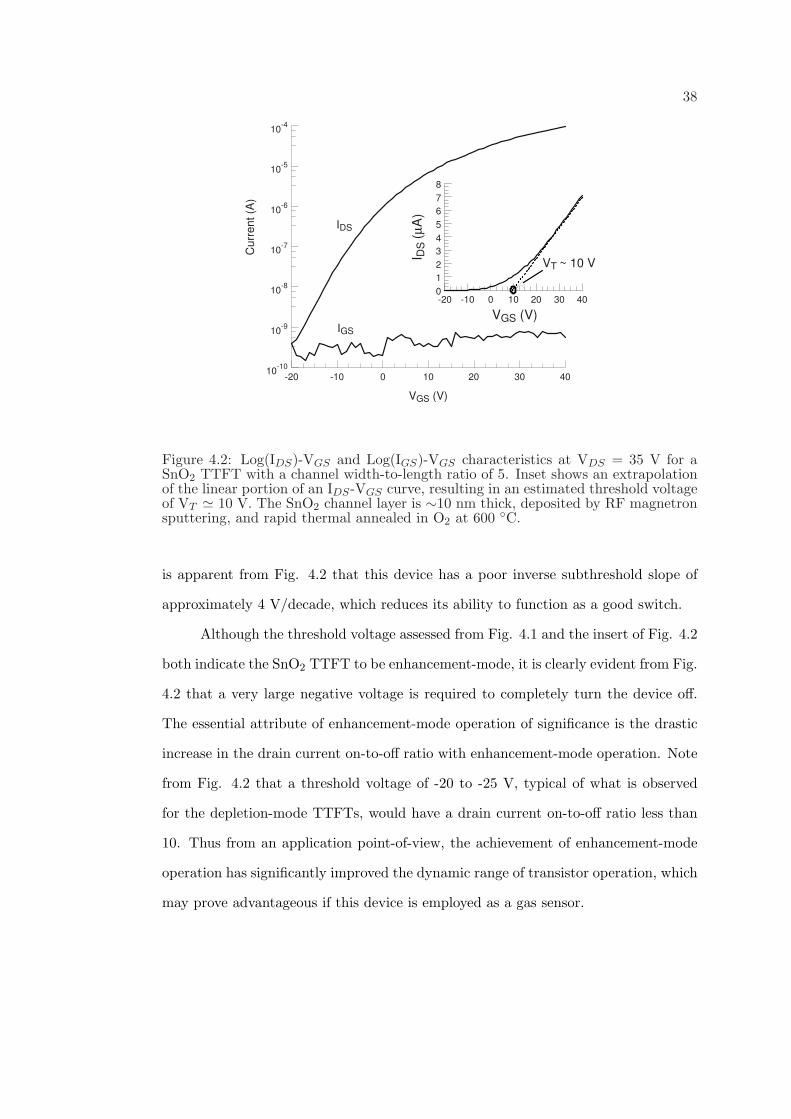
38
IDS
IGS
10-10
10-9
10-8
10-7
10-6
10-5
10-4
Curr
ent
(A)
-20 -10 0 10 20 30 40
VGS (V)
VT ~ 10 V
0
1
2
3
4
5
6
7
8
I DS
(µA
)
-20 -10 0 10 20 30 40
VGS (V)
Figure 4.2: Log(IDS)-VGS and Log(IGS)-VGS characteristics at VDS = 35 V for aSnO2 TTFT with a channel width-to-length ratio of 5. Inset shows an extrapolationof the linear portion of an IDS-VGS curve, resulting in an estimated threshold voltageof VT ' 10 V. The SnO2 channel layer is ∼10 nm thick, deposited by RF magnetronsputtering, and rapid thermal annealed in O2 at 600 ◦C.
is apparent from Fig. 4.2 that this device has a poor inverse subthreshold slope of
approximately 4 V/decade, which reduces its ability to function as a good switch.
Although the threshold voltage assessed from Fig. 4.1 and the insert of Fig. 4.2
both indicate the SnO2 TTFT to be enhancement-mode, it is clearly evident from Fig.
4.2 that a very large negative voltage is required to completely turn the device off.
The essential attribute of enhancement-mode operation of significance is the drastic
increase in the drain current on-to-off ratio with enhancement-mode operation. Note
from Fig. 4.2 that a threshold voltage of -20 to -25 V, typical of what is observed
for the depletion-mode TTFTs, would have a drain current on-to-off ratio less than
10. Thus from an application point-of-view, the achievement of enhancement-mode
operation has significantly improved the dynamic range of transistor operation, which
may prove advantageous if this device is employed as a gas sensor.

39
0
20
40
60
80
100
Tra
nsm
itta
nce
(%)
200 300 400 500 600 700 800
Wavelength (nm)
900
(b)
(a)
Figure 4.3: Optical transmittance as viewed through the ITO source/drain and thechannel of a SnO2 TTFT. Curve (a) is corrected for reflectance, i.e., T / (1 - R),whereas curve (b) is the raw transmission through the entire stack, including thesubstrate. Inset illustrates the bottom-gate TTFT structure and biasing schemeemployed.
As seen from the IDS-VDS curves shown in Fig.4.1, the TTFT exhibits a maxi-
mum drain current near 90 µA, a modest value for a TTFT with a channel width-to-
length ratio of 5. The magnitude of IDS depends on the mobility of the electrons in
the channel. The maximum effective mobility [7] for the enhancement-mode device
corresponding to Fig. 4.1 is equal to 0.8 cm2V−1s−1. The maximum effective mobility
is 2 cm2V−1s−1 for the depletion-mode SnO2 TTFTs.
The optical transmittance versus wavelength through the ITO source/drain
and channel of a SnO2 TTFT is shown in Fig. 4.3. Curve (a) is the transmittance
corrected for reflectance, i.e., T / (1 - R), indicating an average transmission of ∼90%
across the visible spectrum (400-700 nm). Curve (b) is the raw transmittance through
the entire stack, including the substrate, indicating an average transmission of ∼75%
across the visible spectrum.

40
0 20 40 60 80
SnO2
Inte
nsity
(a.u
.)
sputtered, 600oC furnace, ~300 nm
sputtered, 600oC RTA, ~300 nm
N2
plasma, 600oC furnace, ~200 nm
2 θ (degrees)
Figure 4.4: X-ray diffraction patterns obtained from two sputter-deposited SnO2 thinfilms which are either furnace or rapid thermal annealed (RTA) at 600◦C, and for aSnO2 thin film prepared by evaporation of SnO2 powder in a ∼ 5×10⁻⁴ Torr pressureof microwave-activated N2 and subsequently furnace annealed at 600◦C. The post-deposition anneal leads to increased crystallinity of the sputtered films, whereas filmsprepared by activated reactive evaporation in N2 remain amorphous after annealing.
It is very difficult to fabricate enhancement-mode SnO2 TTFTs. Although
the ’as deposited’ SnO2 thin films are invariably extremely insulating, they exhibit
little or no gate modulation when employed as TTFT channel layers due to poor
crystallinity, thus requiring a post-deposition anneal.
Figure 4.4 shows an X-ray diffraction (XRD; performed with a Siemens D-5000
X-ray diffractometer using Cu Kα radiation) comparison of two sputter-deposited
SnO2 thin films, which are heated at 600 ◦C with a furnace or RTA. Peak identification
confirms these films to be SnO2. Assessment of the XRD peak widths, using the
Scherrer formula and a Lorentzian peak shape, yields an estimated average crystal
size of 11 nm (furnace) and 7.5 nm (RTA), whereas Williamson-Hall plots give average
crystal size, strain estimates of 17.1 nm, 0.023% (furnace) and 16.5 nm, 0.036% (RTA)
41
[30]. The Williamson-Hall analysis suggests that the RTA film is more strained than
the furnace annealed film, and that the Scherrer formula significantly underestimates
the crystal size due to the neglect of strain.
Improving the crystallinity of the SnO2 thin film via a post-deposition anneal
does not ensure enhancement-mode TTFT behavior. Typically the annealed SnO2
thin films are too conductive for TTFT applications, presumably due to the ten-
dency of SnO2 to form oxygen vacancies, which are shallow double-donors providing
conduction-band electrons [31, 32]. Often the channel-layer conductivity is so high, to
many free carriers, that it cannot be appreciably modulated by a gate voltage, making
transistor operation impossible. If the channel-layer conductivity is sufficiently low-
ered, transistor behavior is possible, although such TFTs operate in depletion-mode
unless the conductivity can be decreased to an appropriate level.
Several methods for reducing the conductivity of the SnO2 channel layer have
been explored. One approach is to evaporate SnO2 powder in a partial pressure of
microwave-activated N2. The idea here is to incorporate nitrogen into the SnO2 film,
since nitrogen substitution onto an oxygen atomic site results in acceptor doping
which would compensate oxygen vacancies or other SnO2 donors, thereby reduc-
ing both the carrier concentration and the conductivity of the film. Although films
prepared in this manner are indeed highly resistive, they unfortunately remain amor-
phous after heat treatment at 600 ◦C. Thus, TTFTs fabricated with such films as
channel layers do not exhibit transistor action, presumably due to the very poor mo-
bility of these amorphous films. Figure 4.4 includes the XRD pattern of such a film,
confirming its amorphous nature. Compensation of SnO2 films by indium diffusion
doping was also explored, since indium substitution onto a tin atomic site also results
in acceptor doping. Although indium incorporation into the SnO2 film did result in a
decrease in conductivity, as expected, this decrease was not sufficient to achieve the
required degree of conductivity control of the channel. To date, the most successful
approach for minimizing the channel-layer conductivity is to increase the resistance
42
of a relatively conductive SnO2 channel by simply decreasing the channel thickness;
this is the motivation for employing very thin channel layers (∼10-20 nm).
4.3 Conclusions
A highly transparent SnO2 TTFT with prototypical IDS-VDS characteristics,
a modest channel mobility, and enhancement-mode behavior has been fabricated.
The enhancement-mode nature of these SnO2 TTFTs results in an IDS on-to-off
ratio of ∼ 105, which is approximately four orders of magnitude larger than that
of a depletion-mode device. This improvement in the IDS on-to-off ratio should
dramatically increase the dynamic range of SnO2 TFT gas sensors as proposed by
Wollenstein et al [33]. Moreover, the transparent nature of SnO2 TTFTs may lead
to improved sensor performance and new sensor applications, since heterogeneous
processes occurring at the active sensor surface may be optically stimulated or probed
from the sensor side opposite gas/analyte exposure.

43
5. TRANSPARENT CIRCUITS
This chapter is devoted to a discussion of the fabrication and characterization
of transparent circuits including, inverters and ring oscillators.
5.1 Transparent circuit fabrication
Transparent circuits are fabricated using a staggered, bottom-gate TFT config-
uration; the fabrication process includes seven primary steps and employs four mylar
masks (CAD/Art Services, Inc.). A schematic representation of an inverter cross-
section and a plan view of a transparent inverter are shown in Fig. 5.1. The process
begins with a Corning 1737 glass substrate, coated with ∼200 nm sputtered indium
tin oxide (ITO, Delta Technologies).
1. Mask A: Gate electrodes are defined using standard photolithographic pattern-
ing and an 11.8M hydrochloric acid (HCl) wet etch. The etch rate is ∼0.33
nm/sec.
2. The silicon dioxide gate dielectric layer (∼100 nm) is deposited via plasma-
enhanced chemical vapor deposition (PECVD) using SiH4 + He and N2O pre-
cursors.
3. Mask B: Contact to the gate electrodes is established through vias opened using
photolithography and reactive ion etching.
4. The IGO channel layer (40-50 nm) is deposited by rf magnetron sputtering from
a 2 inch target (Cerac, Inc.; 1:1 molar ratio of In2O3:Ga2O3). Process pressure,
process ambient, rf power density, and target-to-substrate distance are 5 mTorr,
Ar/O2 (90%/10%), ∼3.7 Wcm−2, and ∼10 cm, respectively.
5. Mask C: The channel is patterned using an ∼2M HCl wet etch. The etch rate
is ∼0.63 nm/sec.
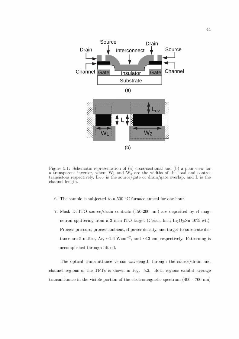
44
���������������������������������������������������������������������������������������������������������������������������������������������������������������������������������������������������������������������������������������������������������������������������������������������������������������������������������������������������������������������������������������������������������������������������������������������������������������������������������������������������������������������������������������������������������������������������������������������������������������������������������������������������������������������������
���������������������������������������������������������������������������������������������������������������������������������������������������������������������������������������������������������������������������������������������������������������������������������������������������������������������������������������������������������������������������������������������������������������������������������������������������������������������������������������������������������������������������������������������������������������������������������������������������������������������������������������������������������������������������������������������������������������������������������������������������������������������������������������������������������������������������������������������������������������������������������������������������������������������������������������
Insulator
(a)
���
L���������
W1 �
�������������������������
W2
���
Lov
(b)
���
Substrate
GateGateChannel Channel
������� �������
Source
DrainDrain
SourceInterconnect�������
����
���
���
���������
���
����
����
����
����
Figure 5.1: Schematic representation of (a) cross-sectional and (b) a plan view fora transparent inverter, where W1 and W2 are the widths of the load and controltransistors respectively, LOV is the source/gate or drain/gate overlap, and L is thechannel length.
6. The sample is subjected to a 500 ◦C furnace anneal for one hour.
7. Mask D: ITO source/drain contacts (150-200 nm) are deposited by rf mag-
netron sputtering from a 3 inch ITO target (Cerac, Inc.; In2O3:Sn 10% wt.).
Process pressure, process ambient, rf power density, and target-to-substrate dis-
tance are 5 mTorr, Ar, ∼1.6 Wcm−2, and ∼13 cm, respectively. Patterning is
accomplished through lift-off.
The optical transmittance versus wavelength through the source/drain and
channel regions of the TFTs is shown in Fig. 5.2. Both regions exhibit average
transmittance in the visible portion of the electromagnetic spectrum (400 - 700 nm)
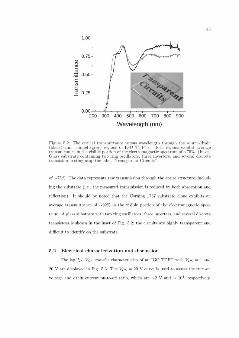
45
200 300 400 500 600 700 800 9000.00
0.25
0.50
0.75
1.00
Tra
nsm
ittan
ce
Wavelength (nm)
Figure 5.2: The optical transmittance versus wavelength through the source/drain(black) and channel (grey) regions of IGO TTFTs. Both regions exhibit averagetransmittance in the visible portion of the electromagnetic spectrum of ∼75%. (Inset)Glass substrate containing two ring oscillators, three inverters, and several discretetransistors resting atop the label “Transparent Circuits”.
of ∼75%. The data represents raw transmission through the entire structure, includ-
ing the substrate (i.e., the measured transmission is reduced by both absorption and
reflection). It should be noted that the Corning 1737 substrate alone exhibits an
average transmittance of ∼92% in the visible portion of the electromagnetic spec-
trum. A glass substrate with two ring oscillators, three inverters, and several discrete
transistors is shown in the inset of Fig. 5.2; the circuits are highly transparent and
difficult to identify on the substrate.
5.2 Electrical characterization and discussion
The log(ID)-VGS transfer characteristics of an IGO TTFT with VDS = 1 and
20 V are displayed in Fig. 5.3. The VDS = 20 V curve is used to assess the turn-on
voltage and drain current on-to-off ratio, which are ∼2 V and ∼ 104, respectively.
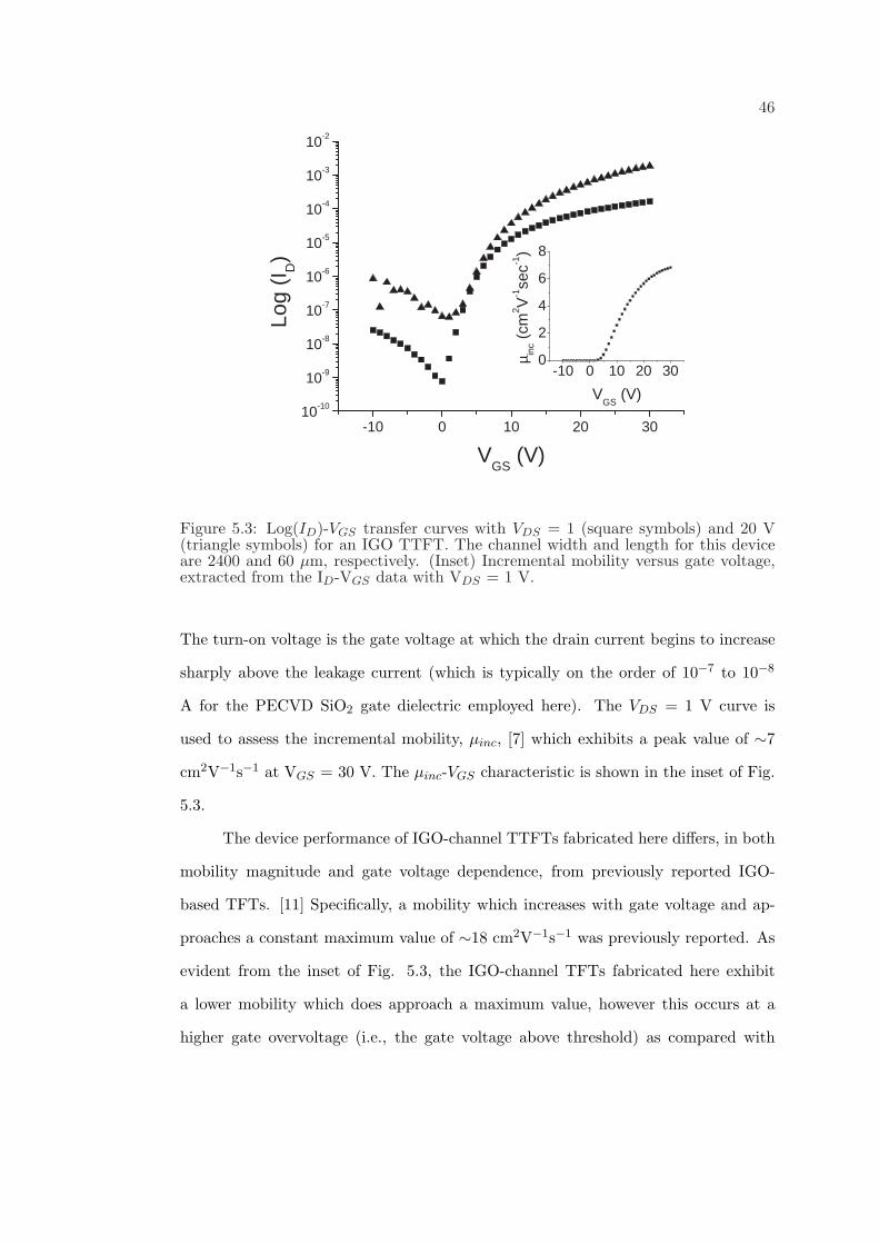
46
-10 0 10 20 3010-10
10-9
10-8
10-7
10-6
10-5
10-4
10-3
10-2
-10 0 10 20 300
2
4
6
8
Log
(ID)
VGS
(V)
µ inc (
cm2 V
-1se
c-1)
VGS
(V)
Figure 5.3: Log(ID)-VGS transfer curves with VDS = 1 (square symbols) and 20 V(triangle symbols) for an IGO TTFT. The channel width and length for this deviceare 2400 and 60 µm, respectively. (Inset) Incremental mobility versus gate voltage,extracted from the ID-VGS data with VDS = 1 V.
The turn-on voltage is the gate voltage at which the drain current begins to increase
sharply above the leakage current (which is typically on the order of 10−7 to 10−8
A for the PECVD SiO2 gate dielectric employed here). The VDS = 1 V curve is
used to assess the incremental mobility, µinc, [7] which exhibits a peak value of ∼7
cm2V−1s−1 at VGS = 30 V. The µinc-VGS characteristic is shown in the inset of Fig.
5.3.
The device performance of IGO-channel TTFTs fabricated here differs, in both
mobility magnitude and gate voltage dependence, from previously reported IGO-
based TFTs. [11] Specifically, a mobility which increases with gate voltage and ap-
proaches a constant maximum value of ∼18 cm2V−1s−1 was previously reported. As
evident from the inset of Fig. 5.3, the IGO-channel TFTs fabricated here exhibit
a lower mobility which does approach a maximum value, however this occurs at a
higher gate overvoltage (i.e., the gate voltage above threshold) as compared with
47
previously reported IGO channel TFTs. These differences are attributed primarily
to differences in the gate dielectric. Previously reported IGO-channel TFTs employ
thermally grown silicon dioxide, whereas the fabrication process reported here uses
PECVD silicon dioxide. Similar observations have been reported for other material
systems; Nomura et al. observed a dramatic difference in TFT channel mobility be-
tween aluminum oxide and hafnium oxide gate dielectric layers. [17] Additionally,
non-idealities associated with photolithographic processing, including residual pho-
toresist or interaction of the surface with photoresist and associated chemicals may
impact device performance.
The transfer characteristic for a transparent inverter is shown in Fig. 5.4.
The inverters consist of two n-channel IGO TTFTs: a control transistor and a load
transistor. In Fig. 5.4, the gate and drain of the load transistor (Vload and VDD,
respectively) are biased at 30 V. The width and length of the control transistor are
2400 µm and 60 µm, respectively; the width and length of the load transistor are 600
µm and 60 µm, respectively.
The inverter shown in Fig. 5.4 exhibits the requisite characteristics needed
to fabricate a ring oscillator using n-channel transistors, without the use of level-
shifting circuitry. First, the switching voltage (the input voltage at which the output
voltage begins to decrease) occurs at a positive Vin value; this ensures that the control
transistor can be shut off during ring oscillator operation and corresponds to a positive
turn-on voltage for the control transistor. Additionally, the peak gain magnitude
(—dVout/dVin—) is ∼1.5 for the transfer curve shown in Fig. 5.4; a gain magnitude
greater than 1 is required for sustained signal propagation (i.e., switching of the next
inverter). The gain is affected by the ratio between drive and load TFT impedance
and is thus affected by the channel mobility, device geometry, and biasing conditions.
The inset of Fig. 5.4 shows the inverter gain as a function of VDD (with Vload = VDD)
for an IGO-based inverter; as VDD is increased from 10 to 35 V, the inverter gain
increases with increasing VDD.

48
0.75
1.00
1.25
1.50
1.75
Gai
n
10 15 20 25 30 35
VDD (V)
0
5
10
15
20
25
30
Vo
ut (
V)
-5 0 5 10 15 20 25
Vin (V)
30
Figure 5.4: Transfer curve for a transparent inverter fabricated using IGO TTFTsand with VDD and Vload = 30 V. (Inset) Inverter gain magnitude as a function ofVDD.
A ring oscillator consists of any odd number of inverters connected in series;
here, a five-stage ring oscillator circuit is employed. The oscillation frequency as a
function of VDD is shown in Fig. 5.5 (in all cases, Vload is equivalent to VDD). As ex-
pected, the oscillation frequency increases as VDD increases; the maximum frequency
of oscillation is ∼9.5 kHz for VDD = 80 V. This corresponds to an propagation delay
of 10.5 µs. A linear trendline is overlaid on the data, showing a nearly linear depen-
dence of the oscillation frequency on VDD; the deviation from linearity at low-VDD
is a consequence of the non-ideal VGS dependence observed in the channel mobility
(shown in the inset of Fig. 5.3).
The inset of Fig. 5.5 shows the output characteristic of a five-stage transparent
ring oscillator, with Vload and VDD = 30 V. Measurements are obtained through an
output inverter stage which is used for non-intrusive electrical probing. The DC offset
voltage is ∼11 V and the peak-to-peak voltage and frequency of oscillation are ∼6.6
V and ∼2.2 kHz, respectively.

49
0
2
4
6
8
10
Fre
qu
ency
(kH
z)
10 20 30 40 50 60 70 80
VDD (V)
-500 0 500Time (µµµµs)
7
11
15
Vo
ut (
V)
Figure 5.5: Oscillation frequency as a function of VDD for a five-stage ring oscillatorfabricated using IGO TTFTs. (Inset) Output characteristic of the transparent ringoscillator when VDD = Vload = 30 V.
The oscillation frequency of these IGO-based ring oscillators is significantly
affected by the device and circuit structure. For ease of fabrication, a relatively
large source/gate and drain/gate overlap of 200 µm is employed, adding a large
parasitic capacitance of ∼141.7 nF/cm to each TTFT, which directly reduces the
frequency of oscillation. In addition, the observed VGS dependence of the channel
mobility effects the oscillation frequency. SPICE simulations suggest that a ring
oscillator with structure and layout as reported here, with a channel mobility of 7
cm2V−1s−1 and biased at VDD = 30 V, should have an oscillation frequency of∼8 kHz,
approximately four times larger than the measured frequency. However, the use of the
peak incremental channel mobility (7 cm2V−1s−1) is inappropriate for this simulation,
as it is not representative of the “operational” mobility of devices operating in this
circuit. Instead, if the average of the incremental mobility over the voltage swing of
the ring oscillator is assessed, a more appropriate value of 2.55 cm2V−1s−1 is obtained.

50
0 10 20 30 40 50 60
Channel length (µm)
0
20
40
60
80
100
120
140
160
Fre
quency
(kH
z)
Figure 5.6: Oscillation frequency as a function of the channel length for a five-stagering oscillator via SPICE simulation using a width-to-length ratio of 40 for the controltransistor, width-to-length ratio of 10 for the load transistor, a overlap capacitanceof 70.8 nFcm−1, mobility of 2.55 cm2V−1s−1 for both transistors, a turn-on voltageof 2 V for both transistors, and biased at 30 V.
When this mobility is used in SPICE simulation, the resultant oscillation frequency
is ∼2.2 kHz, which is identical to the measured value of 2.2 kHz.
Comparing these transparent IGO ring oscillators with the pentacene OFET
ring oscillators presented in Section 2.6, it is evident that these transparent ring
oscillators operate at similar frequencies. However, when the larger device dimen-
sions and much larger parasitic capacitances used in the transparent ring oscillators
are compared to the OFET dimensions discussed in Section 2.6, it is clear that the
transparent ring oscillators have much higher performance.
Figure 5.6 shows the relationship between operating frequency and channel
length as simulated in SPICE. As the channel length decreases, the operating fre-
51
quency increases; this increase is particularly pronounced for gate lengths less than
about 10 µm.
Figure 5.7 illustrates the oscillation frequency dependence on the contact over-
lap as determined from SPICE simulation. As the contact overlap decreases the
frequency increases; this increase is especially significant when the contact overlap is
less than about 40 µm.
Using device geometries common in the OFET ring oscillators discussed in Sec-
tion 2.6, i.e., channel length of 1 µm and a contact overlap of 5 µm, SPICE simulation
indicates that the operating frequency of the transparent IGO ring oscillator would
increase to 5.36 MHz. However, it should be noted that OFET ring oscillators are
fabricated at low temperatures, and are thus compatible with plastic and paper sub-
strates, thereby facilitating fabrication onto flexible substrates. In contrast, the IGO
transparent circuits presented here are processed at a maximum temperature of 500
◦C, making them incompatible with plastic substrates.
5.3 Conclusions
Highly transparent circuits, including inverters and five-stage ring oscillators,
are fabricated using photolithographic patterning techniques; seven primary steps
and four masks are required in the fabrication process. The resulting five-stage ring
oscillators operate at a frequency of ∼2.2 kHz when the gate and drain of the load
transistor are biased at 30 V; the maximum oscillation frequency obtained is ∼9.5
kHz, with the gate and drain of the load transistor biased at 80 V. This demonstra-
tion comprises evidence for the viability of TTFTs based on indium gallium oxide
and, in general, for the viability of oxide semiconductor TTFTs within the emerging
transparent electronics arena.

52
0 50 100 150 200
contact overlap (µm)
0
5
10
15
20
25
Fre
quency
(kH
z)
30
Figure 5.7: Oscillation frequency as a function of the contact overlap for a five-stage ring oscillator using SPICE with a width-to-length ratio of 40 for the controltransistor, a width-to-length ratio of 10 for the load transistor, a channel length of60 µm, a mobility of 2.55 cm2V−1s−1 for both transistors, a turn-on voltage of 2 Vfor both transistors, and biased at 30 V.
53
6. CONCLUSIONS AND RECOMMENDATIONS FOR FUTUREWORK
6.1 Conclusions
This thesis focuses on two aspects of transparent electronics, SnO2 TTFTs
and transparent circuits. Conclusions related to these two areas are summarized as
follows.
First, the fabrication procedure and electrical characteristics of SnO2 TTFTs
are presented. Both depletion- and enhancement-mode devices are realized. The
maximum effective mobility for the depletion- and enhancement-mode devices are
2 cm2V−1s−1 and 0.8 cm2V−1s−1, respectively. A variety of techniques to decrease
the carrier concentration in the SnO2 channel are investigated, includng compensa-
tion doping using indium and nitrogen. Both of these techniques are found to be
unsuccessful for decreasing the carrier concentration to an acceptable level in order
to create an enhancement-mode TTFT. Decreasing the channel thickness, which ef-
fectively decreases the channel conductivity, is the procedure employed for successful
realization of an enhancement-mode TTFT.
Second, the fabrication procedure and the electrical characteristics of trans-
parent circuits, which include inverters and ring oscillators, are presented. These
circuits are highly transparent, exhibiting ∼75% optical transmittance in the visible
portion of the electromagnetic spectrum, and are fabricated using indium gallium
oxide as the active channel material and standard photolithography techniques. The
n-channel indium gallium oxide thin-film transistors exhibit a peak incremental mo-
bility of ∼7 cm2V−1s−1 and a turn-on voltage of ∼2 V. A five-stage ring oscillator
circuit (which does not employ level-shifting) is fabricated, and exhibits an oscillation
frequency of ∼2.2 kHz with the gate and drain of the load transistor biased at 30 V;
54
the maximum oscillation frequency observed is ∼9.5 kHz, with the gate and drain of
the load transistor biased at ∼80 V.
6.2 Recommendations for future work
The purpose of this section is to summarize recommended directions of future
work based on findings presented in this thesis.
More work should be undertaken to optimize the performance of SnO2 TTFTs.
The use of the SnO2 TTFTs as active gas sensors should be investigated. An etch
process to pattern the SnO2 channel needs to be developed to ease device integration.
Also, device dimensions should be reduced using photolithographic patterning.
The transparent circuits presented in this thesis are based on exclusive use
of IGO as a channel material. There are many other possible channel materials.
Future work should investigate other transparent semiconductors as possible channel
materials. Also, the work presented in this thesis utilized large device dimensions
to ease device fabrication. Layout optimization and decreasing device size should be
investigated for improving circuit performance.
This work demonstrates the ability to use conventional photolithography tech-
niques to integrate these wide band gap semiconductors into viable circuits. Further
work should be pursued to develop a ”tool box” of both digital and analog building
block components in order to further demonstrate the viability of these materials.
This tool box could include, but is not limited to the following components: NAND
gate, static D-flip-flop, frequency divider (a cascade of D-flip-flops), common-source
amplifier, differential amplifier, current mirror, and a 2-stage operational amplifier.
55
BIBLIOGRAPHY
1. P. F. Carcia, R. S. McLean, M. H. Reily, and G. Nunes, “Transparent ZnOthin-film transistor fabricated by rf magnetron sputtering,” Appl. Phys. Lett.,vol. 82, pp. 1117–1119, 2003.
2. R. L. Hoffman, B. J. Norris, and J. F. Wager, “ZnO-based transparent thin-filmtransistors,” Appl. Phys. Lett., vol. 82, pp. 733–735, 2003.
3. S. Masuda, K. Kitamura, Y. Okumura, S. Miyatake, H. Tabata, and T. Kawai,“Transparent thin film transistors using ZnO as an active channel layer and theirelectrical properties,” J. Appl. Phys., vol. 93, pp. 1624–1630, 2003.
4. J. Nishii, F. M. Hossain, S. Takagi, T. Aita, K. Saikusa, Y. Ohmaki,I. Ohkubo, S. Kishimoto, A. ira Ohtomo, T. Fukumura, F. Matsukura, Y. Ohno,H. Koinuma, A. H. Ohno, and M. Kawasaki, “High mobility thin film transistorswith transparent ZnO channels,” Jpn. J. Appl. Phys., vol. 42, pp. L347–L349,2003.
5. B. J. Norris, J. Anderson, J. F. Wager, and D. A. Keszler, “Spin-coated zincoxide transparent transistors,” J. Phys. D: Appl. Phys., vol. 36, pp. L105–L107,2003.
6. J. F. Wager, “Transparent electronics,” Science, vol. 300, pp. 1245–1246, 2003.
7. R. L. Hoffman, “ZnO-channel thin-film transistors: Channel mobility,” J. Appl.Phys., vol. 95, pp. 5813–5819, 2004.
8. H. Hosono, N. Kikuchi, N. Ueda, and H. Kawazoe, “Working hypothesis toexplore novel wide band gap electrically conducting amorphous oxides and ex-amples,” J. Non-Cryst. Sol., vol. 165, pp. 198–200, 1996.
9. H. Hosono, M. Yasukawa, and H. Kawazoe, “Novel oxide amorphous semiconduc-tors: transparent conducting amorphous oxides,” J. Non-Cryst. Sol., vol. 203,p. 334, 1996.
10. S. Narushima, M. Orita, M. Hirano, and H. Hosono, “Electronic structureand transport properties in the transparent amorphous oxide semiconductorcadmium oxide-germanium oxide,” Phys. Rev. B: Condens. Matter, vol. 66,p. 035203, 20032.
11. H. Q. Chiang, J. F. Wager, R. L. Hoffman, J. Jeong, and D. A. Keszler, “Highmobility transparent thin-film transistors with amorphous zinc tin oxide channellayer,” Appl. Phys. Lett., vol. 86, 2005.

56
12. N. L. Dehuff, E. S. Kettenring, D. Hong, H. Q. Chiang, J. F. Wager, R. L.Hoffman, C.-H.Park, and D. A. Keszler, “Transparent thin-film transistors withzinc indium oxide channel layer,” J. Appl. Phys., vol. 97, pp. 064505–1 – 064505–5, 2005.
13. A. S. Sedra and K. C. Smith, Microelectronic Circuits. Oxford, New York:Oxford University Press, fourth ed., 1998.
14. Y. Kwon, Y. Li, Y. W. Heo, M. Jones, P. H. Holloway, D. P. Norton, Z. V. Park,and S. Li, “Enhancement-mode thin-film field-effect transistor using phosphorus-doped (zn,mg)o channel,” Appl. Phys. Lett., vol. 84, pp. 2685–2687, 2004.
15. A. Aoki and H. Sasakura, “Tin oxide thin film transistors,” Jpn. J. Appl. Phys.,vol. 9, p. 582, 1970.
16. M. W. J. Prins, K.-O. Grosse-Holz, G. Muller, J. F. M. Cillessen, J. B. Gies-bers, R. P. Weening, and R. M. Wolfd, “A ferroelectric transparent thin-filmtransistor,” Appl. Phys. Lett., vol. 68, pp. 3650–3652, 1996.
17. K. Nomura, H. Ohta, K. Ueda, T. Kamiya, M. Hirano, and H. Hosono, “Thin-film transistor fabricated in single-crystalline transparent oxide semiconductor,”Science, vol. 300, pp. 1269–1272, 2003.
18. K. Nomura, H. Ohta, A. Takagi, T. Kamiya, M. Hirano, and H. Hosono, “Room-temperature fabrication of transparent flexible thin-film transistors using amor-phous oxide semiconductors,” Nature, vol. 432, pp. 488–492, 2004.
19. M. Batzill and U. Diebold, “The surface and materials science of tin oxide,”Progress in surface science, vol. 79, pp. 47–154, 2005.
20. C. Kittel, Introduction to solid state physics. New York: John Wiley and SonsInc., third ed., 1953.
21. H. Klauk, J. G. D, and T. N. Jackson, “Fast organic thin-film transistor circuits,”IEEE Electron Device Letters, vol. 20, pp. 289–291, 1999.
22. G. H. Gelinck, T. C. T. Geuns, and D. M. de Leeuw, “High-performance all-polymer integrated circuits,” Appl. Phys. Lett., vol. 77, pp. 1487–1489, 2003.
23. M. G. Kane, J. Campi, M. S. Hammond, F. P. Cuomo, B. Greening, C. D.Sheraw, J. A. Nichols, D. J. Gundlach, J. R. Huang, C. C. Kuo, L. Jia, H. Klauk,and T. N. Jackson, “Analog and digital circuits using organic thin-film transis-tors on polyester substrates,” IEEE Electron Device Letters, vol. 21, pp. 534–536,2000.
24. C. D. Sheraw, J. A. Nichols, D. J. Gundlach, J. R. Huang, C. C. Kuo, H. Klauk,T. N. Jackson, M. G. Kane, J. Campi, F. P. Cuomo, and B. K. Greening, “Fastorganic circuits on flexible polymeric substrates,” IEEE International ElectronDevices Meeting, vol. 00, pp. 619–622, 2000.

57
25. U. Zschieschang, H. Klauk, M. Halik, G. Schmid, and C. Dehm, “Flexible organiccircuits with printed gate electrodes,” Advanced materials, vol. 15, pp. 1147–1151, 2003.
26. F. Eder, H. Klauk, M. Halik, U. Zschieschang, G. Schmid, and C. Dehm, “Or-ganic electronics on paper,” Appl. Phys. Lett., vol. 84, pp. 2673–2675, 2004.
27. M. A. Lieberman and A. J. Lichtenberg, Principles of plasma discharges andmaterials processing. New York: John Wiley and Sons Inc., first ed., 1994.
28. S. Wolf and R. N. Tauber, Silicon Processing for the VLSI Era. Sunset Beach,Caifornia: Lattice Press, fourth ed., 2000.
29. D. K. Schroder, Semiconductor Material and Device Characterization. NewYork, New York: John Wiley and Sons Inc., 2nd ed., 1998.
30. B. D. Cullity and S. R. Stock, Elements of X-ray Diffraction. Upper SaddleRiver, NJ: Prentice Hall, 3rd ed., 2001.
31. S. Samson and C. G. Fonstad, “Defect structure and electronic donor levels instannic oxide crystals,” J. Appl. Phys., vol. 44, pp. 4618–4621, 1973.
32. H. L. Hartnagel, A. L. Dawar, A. K. Jain, and C. Jagadish, SemiconductingTransparent Thin Films. Bristol, United Kingdom.: Institute of Physics, 1995.
33. J. Wollenstein, M. Jagle, and H. Bottner, Advanced Gas Sensing, pp. 85–99.Kluwer Academic, 2003.

58
APPENDICES

59
A. PECVD OPERATION PROCEDURE AND
ROUTINE MAINTENANCE
This appendix is divided into two main sections, normal operation and routine
maintenance for the PECVD system in the Advanced Materials Laboratory in Owen
Hall at Oregon State University.
A.1 Normal Operation
This section describes normal operation of the PECVD for depositing silicon
dioxide. It is sub-divided into system startup, film deposition, and system shut-down
sections.
A.1.1 System startup
1. Turn on the cooling water to the vacuum pumps, which are located in the
storage closet.
(a) Trace out the water lines to make sure that you turn on the correct valves
at the back of the chiller.
(b) Open the return valve.
(c) Open the supply valve.
2. Turn on the vacuum pumps. There is one dryvac pump and a RuVac pump in
series for the PECVD system.
(a) Locate an electrical panel with four red light emitting diodes (LEDs) and
two push buttons on the left hand side of the dryvac pump.
(b) Press and hold the back push button so the lighted LED turns-off, this
bypasses the oil pressure interlock.
(c) Press the start button on the electrical box that is labeled ”mechanical
pump”.
(d) Release the push button so the interlocks will be enabled.
60
(e) Wait 1 min, then press the start button on the electrical box labeled
”blower”; this will start the RuVac pump.
3. Turn on the cooling water to the system.
(a) Locate the water valves behind the PECVD system on the wall.
(b) Open the return valve.
(c) Open the supply valve.
(d) Make sure the flow meter on the right hand of the system reads 0.9 gallons
per minute.
4. Set the heater controller to 350 ◦C.
(a) Turn the key on the front of the system to ”modify memory”.
(b) Press and hold the ”set” button on the front of the system.
(c) Press the button labeled ”heater” while still holding down the set button.
(d) Enter the desired temperature (350 ◦C) and press enter.
(e) Turn the key back to manual on the front of the system.
(f) Press and hold the ”manual” button on the front of the system.
(g) Press the button labeled ”heater” while still holding down the manual but-
ton. The heater will turn on and start ramping up to the set temperature,
and will be maintained at that temperature.
5. Rough out the chamber.
(a) Press and hold the manual button.
(b) Press the ”rough” button, while still holding the manual button. This
opens the rough valve and starts to pump the chamber using the mechan-
ical pump.

61
6. Wait until the heater and pressure reach operating values. Wait until the heater
controller on the front of the machine reads 350 ◦C. Also wait until the chamber
pressure is below 1 mTorr.
(a) To check the chamber pressure press and hold the ”read” button on the
front of the system.
(b) Press and hold the ”pressure” button, while still holding the read button.
This will display the chamber pressure.
7. Open the Silane tank.
(a) To access the silane tank open the glass door on the gas cabinet located
to the left of the system.
(b) Open the valve located on the top of the silane tank, do not adjust any of
the other valves in the gas cabinet.
8. Fill the silane delivery line with silane.
(a) Set the flow rate for the silane mass flow controller to 100%.
i. Turn key on the front of the system to modify memory.
ii. Press and hold the set button.
iii. While holing the set button press the desired ”gas” button, silane is
currently connected to the channel labeled ”gas 3”.
iv. Enter the desired flow rate. Note that the display reads in percentage
of the total flow rate for each mass flow controller, so a setting of 100
will set the mass flow controller to the maximum flow rate.
(b) Flow the gas for 5 min to fill the line with silane.
i. Press and hold the manual button.
ii. Press the ”gas 3” button.
9. Do a dummy run to finish filling the silane line with silane.

62
(a) Set the silane flow rate to 10% by following the same procedure as described
in 8a.
(b) Set the nitrous oxide flow rate to 50%, the nitrous oxide is currently con-
nected to the ”gas 2” mass flow controller. The nitrous oxide flow rate is
set the same way as the silane flow rate is adjusted.
(c) Flow the nitrous oxide into the chamber.
i. Press and hold the manual button.
ii. Press the ”gas 2” button.
(d) Increase the chamber pressure to 600 mTorr.
i. Press and hold the manual button.
ii. While holding the manual button press the ”throttle” button.
(e) Wait until the chamber pressure has reached and stabilized around 600 mTorr.
(f) Flow the silane.
i. Press and hold the manual button.
ii. Press the ”gas 3” button.
(g) Wait for the pressure to stabilize around 600 mTorr.
(h) Turn on rf power.
i. Press the rocker switch on the front of the rf power supply to on.
ii. Adjust the rf power to 125 W.
(i) Adjust the matching network.
i. Place the toggle switch on the front of the rf power supply to reflected.
ii. Place the toggle switch on the front of the matching network to man-
ual, and use the buttons labeled ”+” or ”-” to adjust the reflected
power down to zero.
(j) Do a 20 min run to make sure the silane line is completely filled with silane.

63
(k) Turn off he rf power.
i. Press the rocker button on the front of the rf power supply to off.
(l) Stop flowing the silane.
i. Press and hold the manual button.
ii. Press the ”gas 3” button.
(m) Stop flowing the nitrous oxide.
i. Press and hold the manual button.
ii. Press the ”gas 2” button.
(n) Evacuate the chamber to less than 1 mTorr.
i. Press and hold the manual button.
ii. Press the ”throttle” button. This opens the throttle valve and allows
the mechanical pump to evacuate the chamber.
A.1.2 Film Deposition
1. Load the substrates into the chamber.
(a) Vent the chamber.
i. Press and hold down the manual button.
ii. Press the ”rough” button. This will close the rough valve.
iii. Press and hold down the manual button.
iv. Press the ”vent” button.
v. Wait for light next to the vent button to stop flashing.
(b) Turn on the heater.
i. Press and hold the manual button.
ii. Press the heater button.
(c) Raise the hoist.

64
i. Press and hold the manual button.
ii. Press the ”hoist up” button.
(d) Use a dry chemwipe to wipe down the shower head to remove any lose
particles.
(e) Place the substrates into the chamber, for the highest quality dielectric
place only two samples in the chamber at a time and keep them close
to the lamp heater. The ”sweet spot” is located in front of the lamp
heater, but you need to stay away from the edge of the lower electrode by
approximately one inch.
(f) Lower the hoist.
i. Press and hold the manual button.
ii. Press the ”hoist down” button.
(g) Rough out the chamber.
i. Press and hold the manual button.
ii. Press the rough button.
2. Turn on the nitrogen cooling for the lamp heater.
(a) Locate the ball valve on the left side of the system and open the valve.
The leak valve should already be set at a reasonable rate.
3. Flip the switch on the variac that is mounted on the front of the system to on.
4. Slowly turn up the variac until the dial is at 75.
5. Wait for 1 hr for the lamp heater to thoroughly heat the sower head.
6. Set the silane flow rate to 20% by following the same procedure as described in
the startup procedure.
65
7. Set the nitrous oxide flow rate to 100%, the nitrous oxide is currently connected
to the ”gas 2” mass flow controller. The nitrous oxide flow rate is set the same
way as the silane flow rate is adjusted.
8. Flow the nitrous oxide into the chamber.
(a) Press and hold the manual button.
(b) Press the ”gas 2” button.
9. Increase the chamber pressure to 600 mTorr.
(a) Press and hold the manual button.
(b) While holding the manual button press the ”throttle” button.
10. Wait until the chamber pressure has reached and stabilized around 600 mTorr.
11. Flow the silane.
(a) Press and hold the manual button.
(b) Press the ”gas 3” button.
12. Wait for the pressure to stabilize around 600 mTorr.
13. Turn on rf power.
(a) Press the rocker switch on the front of the rf power supply to on.
(b) Adjust the rf power to 125 W.
14. Adjust the matching network.
(a) Place the toggle switch on the front of the rf power supply to reflected.
(b) Place the toggle switch on the front of the matching network to manual,
and use the buttons labeled ”+” or ”-” to adjust the reflected power down
to zero.

66
15. Deposit the desired thickness of silicon dioxide.
16. Turn off rf power.
(a) Press the rocker button on the front of the rf power supply to off.
17. Stop flowing the silane.
(a) Press and hold the manual button.
(b) Press the ”gas 3” button.
18. Stop flowing the nitrous oxide.
(a) Press and hold the manual button.
(b) Press the ”gas 2” button.
19. Turn off the lamp heater.
(a) Slowly turn down the variac to zero.
(b) Flip the toggle switch on the variac to off.
20. Turn off the nitrogen cooling for the lamp heater.
(a) Locate the ball valve on the left side of the system, and close the valve.
21. Evacuate the chamber to less than 1 mTorr.
(a) Press and hold the manual button.
(b) Press the ”throttle” button. This will open the throttle valve and allow
the mechanical pump to evacuate the chamber.
22. Retrieve your samples.
(a) Vent the chamber.
i. Press and hold down the manual button.
ii. Press the ”rough” button. This will close the rough valve.

67
iii. Press and hold down the manual button.
iv. Press the ”vent” button.
v. Wait for light next to the vent button to stop flashing.
(b) Turn on the heater
i. Press and hold the manual button.
ii. Press the heater button.
(c) Raise the hoist.
i. Press and hold the manual button.
ii. Press the ”hoist up” button.
(d) Retrieve your substrates. Note that the substrates are at 350 ◦C so do not
place on anything that will melt.
(e) Lower the hoist.
i. Press and hold the manual button.
ii. Press the ”hoist down” button.
(f) Rough the chamber out.
i. Press and hold the manual button.
ii. Press the rough button.
A.1.3 System shutdown
1. Make sure the chamber pressure is below 1 mTorr, and the rough valve is open,
red light next to the rough button is on.
2. Fill silane line with nitrogen.
(a) Close the valve on the top of the silane tank.
(b) Set the mass flow controller for the silane line to 100%. Follow the same
procedure for adjusting flow rate as described in the previous section.

68
(c) Flow the silane, which is now off at the tank and filling with nitrogen, for
20 min.
(d) Close the valve on top of the nitrogen tank located to the left of the system.
(e) Wait for the pressure in the chamber, and all the way back to the nitrogen
tank to get below 1 mTorr.
(f) Open the valve on top of the nitrogen tank.
(g) Continue to flow the nitrogen for 5 min to completely fill the silane line
with nitrogen.
(h) Turn off the silane mass flow controller.
3. Wait for the chamber pressure to get below 1 mTorr.
4. Close the rough valve.
(a) Press and hold the manual button.
(b) Press the ”rough” button.
5. Turn off the cooling water to the system. Note when the cooling water is shut-off
the system will start to beep.
(a) Close the supply valve that is located on the wall.
(b) Close the return valve located on the wall.
6. Press the stop button on the front of the machine to stop the beeping.
7. Turn off vacuum pumps located in the storage closet.
(a) Press the stop button that is located on the electrical panel labeled ”blower”.
(b) Wait 1 min.
(c) Press the stop button that is located on the electrical panel labeled ”me-
chanical pump”

69
(d) Wait 5 min for pumps to cool.
(e) Turn off cooling water to pumps.
i. Trace the water lines from the pumps to the back of the chiller.
ii. Turn off the supply valve.
iii. Turn off the return valve. Note that it is important that you only turn
off these two valves and the chiller must stay on.
A.2 Routine maintenance
This section describes maintenance procedures that need to be performed pe-
riodically in order to maintain high quality dielectrics. Note that this maintenance
involves the use of hazardous chemicals, hydrofluoric acid, and should only be pre-
formed by qualified personnel. Also note that reinstalling the o-ring requires two
people.
1. Turn on pumps as described in the startup procedure.
2. Rough chamber to less than 1 mTorr.
3. Vent chamber.
4. Raise the hoist.
5. Remove shower head.
(a) Loosen all the allen bolts that hold up the shower head.
(b) Remove all but two of the allen bolts on either side of the shower head.
(c) Hold up on the shower head with one hand while removing the final two
bolts.
(d) Lower the shower head and remove from chamber.
6. Put on all appropriate chemical safety equipment.
70
7. Under a fume hood use hydrofluoric acid to etch the deposited silicon dioxide
from the shower head.
8. Using hydrofluoric acid etch off the deposited silicon dioxide from the lower
platen and chamber walls. Note a respirator has to be worn during this process
since this will be preformed outside of a fume hood.
9. With the help of another person reinstall the shower head, making sure the
o-ring stays in the o-ring grove.
10. Tighten the allen bolts in a star configuration, to avoid warping of the shower
head.
11. Lower hoist
12. Rough chamber.
13. Turn on heater.
14. Wait for chamber pressure to be less than 1 mTorr.
15. Turn on lamp cooling nitrogen.
16. Turn on lamp heater, to 75 on the variac.
17. Bake chamber for 1 hour.
18. Run the ”freon etch” recipe that is located in the log book for the system. This
will remove any residual silicon dioxide missed during the cleaning.
19. Do a 20 min dummy run, described in the startup procedure, before depositing
silicon dioxide onto your substrates.
20. Turn off the lamp heater.
21. Turn off the nitrogen cooling for the lamp heater.
22. Follow the shutdown procedure if you are not depositing any films.