an-8015 fms6501 evaluation board application note
TRANSCRIPT

To learn more about ON Semiconductor, please visit our website at www.onsemi.com
Is Now Part of
ON Semiconductor and the ON Semiconductor logo are trademarks of Semiconductor Components Industries, LLC dba ON Semiconductor or its subsidiaries in the United States and/or other countries. ON Semiconductor owns the rights to a number of patents, trademarks, copyrights, trade secrets, and other intellectual property. A listing of ON Semiconductor’s product/patent coverage may be accessed at www.onsemi.com/site/pdf/Patent-Marking.pdf. ON Semiconductor reserves the right to make changes without further notice to any products herein. ON Semiconductor makes no warranty, representation or guarantee regarding the suitability of its products for any particular purpose, nor does ON Semiconductor assume any liability arising out of the application or use of any product or circuit, and specifically disclaims any and all liability, including without limitation special, consequential or incidental damages. Buyer is responsible for its products and applications using ON Semiconductor products, including compliance with all laws, regulations and safety requirements or standards, regardless of any support or applications information provided by ON Semiconductor. “Typical” parameters which may be provided in ON Semiconductor data sheets and/or specifications can and do vary in different applications and actual performance may vary over time. All operating parameters, including “Typicals” must be validated for each customer application by customer’s technical experts. ON Semiconductor does not convey any license under its patent rights nor the rights of others. ON Semiconductor products are not designed, intended, or authorized for use as a critical component in life support systems or any FDA Class 3 medical devices or medical devices with a same or similar classification in a foreign jurisdiction or any devices intended for implantation in the human body. Should Buyer purchase or use ON Semiconductor products for any such unintended or unauthorized application, Buyer shall indemnify and hold ON Semiconductor and its officers, employees, subsidiaries, affiliates, and distributors harmless against all claims, costs, damages, and expenses, and reasonable attorney fees arising out of, directly or indirectly, any claim of personal injury or death associated with such unintended or unauthorized use, even if such claim alleges that ON Semiconductor was negligent regarding the design or manufacture of the part. ON Semiconductor is an Equal Opportunity/Affirmative Action Employer. This literature is subject to all applicable copyright laws and is not for resale in any manner.

AN-8015 Rev. 1.0
1
www.fairchildsemi.com©2006 Fairchild Semiconductor Corporation
February 2006
AN
-8015 FM
S6501 E
valuatio
n B
oard
Ap
plicatio
n N
ote
AN-8015FMS6501 Evaluation Board Application Note
Description
The FMS6501 evaluation board is a full functional 12x9 crosspoint matrix for evaluating the performance of the FMS6501.The demo board operates from standard supply voltages of +5V±5% and +3.3V ±5%. This device may be driven by a DC-coupledDAC output or an AC-coupled input signal and inputs can beprogrammed for clamp or bias mode. Device outputs can beeither DC or AC coupled and may also be programmed for again of 6, 7, 9 or 12dB. In addition unused outputs may be dis-abled to reduce power dissipation.
The FMS6501 provides 12 inputs that can be routed to any of 9outputs. Each input can be routed to one or more output butonly one input may be routed to any output. Programming of
the FMS6501 is controlled via an I
2
C set of inputs or manualregister and data settings
Applications
Cable and Satellite set top boxes
TV and HDTV sets
A/V switches
Security/surveillance
Personal Video Recorders (PVR)
Video distribution
Automotive (in-cabin entertainment)
For a complete description of the FMS6501 please refer to theFMS6501 data sheet.
Evaluation Board Block Diagram
FMS6501
IN3
IN9
IN8
IN7
IN6
IN5
IN4
IN2
IN1 OUT1
OUT2
OUT3
OUT4
OUT5
OUT6
IN12
IN11
IN10
OUT7
OUT8
OUT9
I2CConnector/
5V GND 5.3V
Address Data

www.fairchildsemi.com
2
AN-8015 Rev. 1.0
AN
-801
5 F
MS
6501
Eva
luat
ion
Bo
ard
Ap
plic
atio
n N
ote
Evaluation Kit Contents
The FMS6501 Evaluation Kit contains the following items:
• AN-8015 – FMS6501 Evaluation Board Application Note
• The latest revision of the FMS6501 data sheet, which also can be obtained from
http://www.fairchildsemi.com
.
• Fully functional FMS6501 eval board
• VIPDEMO™ control software
• Female power connector
Board Setup and Test
The following test equipment is necessary to fully test the FMS6501evaluation board.
• Installed VIPDEMO™ control software for program controlof FMS6501. (follow directions on CD)
• Power supplies +5V ±5%, 250mA and +3.3v ±5%, 250mA
• One high resolution CRT monitor (YC, CV, GBR, Component)
• One HDTV monitor (480I, 480P, 720I, 720P, 1080I)
• One NTSC or PAL video signal source capable of generatingnecessary outputs. (GBR, Y, C, & Composite)
• One PS/HD video signal source capable of generatingnecessary outputs. (480I, 480P 720I, 720P, 1080I)
• One video measurement set (VM700)
• One video measurement set (VM5000)
• Assorted video cables
DO NOT turn on power supply until all connections are completed.
1. Set the power supply 1 to 5.0V and supply 2 to +3.3V.Connect the power supplies to the input voltage terminalsof the demonstration board.
2. Connect G
OUT
signal source to the In1 input BNC connector.
3. Connect B
OUT
signal source to the In2 input BNC connector.
4. Connect R
OUT
signal source to the In3 input BNC connector.
5. Connect G
IN
of monitor to Out1.
6. Connect Bin of monitor to Out2.
7. Connect Rin of monitor to Out3.
8. Turn on the power supplies.
9. Check that address select jumper is in place.This sets device address to 0x 06.
10. Execute VIPDEMO™ control software by clicking on VIPdemo icon. See test setup configuration diagram below.
11. Click “Show Config” button and verify that Bus_Addr is set to 0x06.
12. Program In1 - Bias, In2 - bias and In3 - bias mode.
13. Program In1 to out1, In2 to Out2 and In3 to Out3.
14. Program Out1 6dB, Out2 6dB and Out3 6dB.
15. Program “ON” Out1 enable, Out2, enable andOut3 enable.
16. Verify monitor is setup to receive GBR signals.
17. Verify test pattern that is produced from the signalgenerator is the same as the pattern on the monitor. Example 100% color bars.
18. Testing is now complete
Figure 1. VIPDEMO™ Test Setup Configuration
AN-8015 Rev. 1.0
3
www.fairchildsemi.com
AN
-8015 FM
S6501 E
valuatio
n B
oard
Ap
plicatio
n N
ote
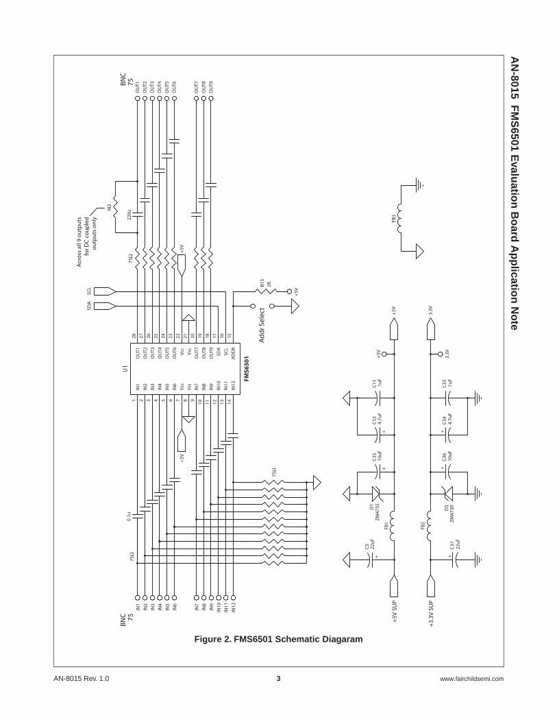
Figure 2. FMS6501 Schematic Diagaram
220u
0.1u
BN
C 7575
Ω
0Ω
75Ω
Ad
dr S
elec
t
BN
C75
75Ω
Acr
oss
all
9 o
utp
uts
for D
C c
ou
ple
do
utp
uts
on
ly
FB1
C35
10u
F
+
D3
ZM
4730
C37
22u
F
+
R13
2K
C34
4.7u
F
+
D1
ZM
4735
C33
.1u
F
U1
FMS6
50
1
C36
10u
F
+
C11
.1u
F
FB3
C5
22u
F
+
C13
4.7u
F
+
FB2
OU
T9
OU
T5
OU
T4
IN6
IN3
OU
T3IN
2O
UT2
OU
T7
IN12
IN10
IN1
IN11
IN9
IN5
OU
T8
OU
T1
IN8
IN4
IN7
OU
T6
+5V
+5V
3.3V
SCL
SDA
+5V
3.3V
+5V
+5V
+5V
SU
P
+3.
3V S
UP
IN1
1
IN2
2
IN3
3
IN4
4
IN5
5
IN6
6
Vcc
7
Vss
8
IN7
9
IN8
10
IN9
11
IN10
12
IN11
13
IN12
14
OU
T128
OU
T227
OU
T326
OU
T425
OU
T524
OU
T623
Vcc
22
Vss
21
OU
T720
OU
T819
OU
T918
SDA
17
SCL
16
AD
DR
15

www.fairchildsemi.com
4
AN-8015 Rev. 1.0
AN
-801
5 F
MS
6501
Eva
luat
ion
Bo
ard
Ap
plic
atio
n N
ote
cloc
k ou
t
load
in
rese
t in
para
llel l
oad
out
LSB
MS
B
LSB
MS
B
Add
ress
Dat
a
SC
L
SD
A
Ack
now
ledg
e
Mom
enta
ry
At U
3,4,
5
88
16 16
At U
1
seria
l out
seria
l out
U4 74HC166
C19 .01
R23 75
Res
et
J3
C31
.001
C1
.01
R17
10K
RP
2
1K
R24 75
Load
J4 J1
R18
10K
RP
1
1KC
1.1
R20
10K
C30
.01
U5 74HC166
C20
.1
J2
C32
.47u
R27 47
0
C18
.01
R21
10K
U3
AC
E15
02
3.3V
3.3V
3.3V
3.3V
3.3V
3.3V
3.3V
+5V
SD
AS
CL
+5V
3.3V
CLK
7
QH
13S
DI
1
CK
E6
H14
G12
F11
E10
D5
C4
B3
A2
CLR
9
PE
15
1 2 3 4 5 6 7 8
16 15 14 13 12 11 10 9
1 2 3 4 5 6 7 8
16 15 14 13 12 11 10 9
1234
CLK
7
QH
13S
DI
1
CK
E6
H14
G12
F11
E10
D5
C4
B3
A2
CLR
9
PE
15
G3
1G
42
NC
3G
64
G7
5G
56
G0
7
Vcc
14G
ND
13N
C12
G2
11N
C10
RE
SE
T/
9G
18
Figure 3. I
2
C Input/Manual Register Data Control Schematic Diagaram

AN-8015 Rev. 1.0
5
www.fairchildsemi.com
AN
-8015 FM
S6501 E
valuatio
n B
oard
Ap
plicatio
n N
ote
Pin Configuration Pin Assignments
Pin# Pin Type Description
1 IN1 Input Input, channel 1
2 IN2 Input Input, channel 2
3 IN3 Input Input, channel 3
4 IN4 Input Input, channel 4
5 IN5 Input Input, channel 5
6 IN6 Input Input, channel 6
7 VCC Input Positive power supply
8 GND Input Must be tied to GND
9 IN7 Input Input, channel 7
10 IN8 Input Input, channel 8
11 IN9 Input Input, channel 9
12 IN10 Input Input, channel 10
13 IN11 Input Input, channel 11
14 IN12 Input Input, channel 12
15 ADDR Input Selects I
2
C address. “0” = 0x06 (0000 0110),“1” = 0x86 (1000 0110)
16 SCL Input Serial clock for I
2
C port
17 SDA Input Serial data for I
2
C port
18 OUT9 Output Output, channel 9
19 OUT8 Output Output, channel 8
20 OUT7 Output Output, channel 7
21 GNDO Input Must be tied to GND
22 VCCO Input Positive power supply for output drivers
23 OUT6 Output Output, channel 6
24 OUT5 Output Output, channel 5
25 OUT4 Output Output, channel 4
26 OUT3 Output Output, channel 3
27 OUT2 Output Output, channel 2
28 OUT1 Output Output, channel 1
1IN1 28 OUT1
2IN2 27 OUT2
3IN3 26 OUT3
4IN4 25 OUT4
5IN5 24 OUT5
6IN6 23 OUT6
7VCC 22 VCCO
8GND 21 GNDO
9IN7 20 OUT7
10IN8 19 OUT8
11IN9 18 OUT9
12IN10 17 SDA
13IN11 16 SCL
14IN12 15 ADDR
FMS650128L SSOP
www.fairchildsemi.com
6
AN-8015 Rev. 1.0
AN
-801
5 F
MS
6501
Eva
luat
ion
Bo
ard
Ap
plic
atio
n N
ote
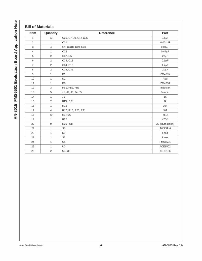
Bill of Materials
Item Quantity Reference Part
1 13 C20, C7-C9, C17-C26 0.1
µ
F
2 1 C31 0.001
µ
F
3 4 C1, CC18, C19, C30 0.01
µ
F
4 1 C32 0.47
µ
F
5 2 C37, C5 22
µ
F
6 2 C33, C11 0.1
µ
F
7 2 C34, C13 4.7
µ
F
8 2 C35, C36 10
µ
F
9 1 D1 ZM4735
10 1 D2 Red
11 1 D3 ZM4730
12 3 FB1, FB2, FB3 Inductor
13 5 J1, J2, J3, J4, J5 Jumper
14 1 J1 1k
15 2 RP2, RP1 2k
16 1 R13 10k
17 4 R17, R18, R20, R21 3M
18 29 R1-R29 75
Ω
19 1 R27 470
Ω
20 9 R30-R38 0
Ω
(stuff option)
21 1 S1 SW DIP-8
22 1 S1 Load
23 1 S2 Reset
24 1 U1 FMS6501
25 1 U3 ACE1502
26 2 U4, U5 74HC166

AN-8015 Rev. 1.0
7
www.fairchildsemi.com
AN
-8015 FM
S6501 E
valuatio
n B
oard
Ap
plicatio
n N
ote
Applications Information
Input Clamp/Bias Circuitry
The FMS6501 can accommodate either AC or DC coupledinputs.
Internal clamping and bias circuitry are provided to support ACcoupled inputs. These are selectable through the CLMP bits viathe I
2
C compatible interface.
For DC coupled inputs, the device should be programmed touse the 'bias' input configuration. In this configuration, the inputis internally biased to 625mV through a 100k
Ω
resistor. Distortionis optimized with the output levels set between 250mV aboveground and 500mV below the power supply. These constraintsalong with the desired channel gain need to be consideredwhen configuring the input signal levels for input DC coupling.
With AC coupled inputs, the FMS6501 uses a simple clamprather than a full DC-restore circuit. For video signals with andwithout sync, (Y,CV,GBR) the lowest voltage at the output pinswill be clamped to approximately 300mV above ground whenthe 6dB gain setting is selected.
If symmetric AC coupled input signals are used, (chroma, Pb,Pr, Cb, Cr) the bias circuit mentioned above can be used to centerthem within the input common range. The average DC value atthe output will be approximately 1.27V with a 6dB gain setting.This value will change, depending upon the selected gain setting.
The following diagram shows the clamp mode input circuit andthe internally controlled voltage at the input pin for AC coupledinputs:
Figure 4. Clamp Mode Input Circuit
The following diagram shows the bias mode input circuit and theinternally controlled voltage at the input pin for AC coupledinputs.
Figure 5. Bias Mode Input Circuit
Output Configuration
The FMS6501 outputs may be either AC or DC coupled. Resis-tive output loads can be as low as 75
Ω
, representing a dualdoubly terminated video load. High impedance, capacitive loadsup to 20pF can also be driven without loss of signal integrity. Forstandard 75
Ω
video loads a 75
Ω
matching resistor should beplaced in series to allow for a doubly terminated load. DC cou-pled outputs should be connected as follows:
Figure 6. DC-Coupled Load Connection
AC-coupled loads should be configured as shown in Figure 6:
Figure 7. AC-Coupled Load Connection
GainSetting
ClampVoltage
BiasVoltage
6dB 300mV 1.27V
7dB 330mV 1.43V
8dB 370mV 1.60V
9dB 420mV 1.80V
FMS6501Input
Clamp
0.1uF
Video sourcemust be
AC-coupledLowest voltage
set to 125mV75Ω
FMS6501InputBias
0.1uF
Video sourcemust be
AC-coupledLowest voltage
set to 625mV75Ω
FMS6501Output
Amplifier
75Ω
75Ω
FMS6501Output
Amplifier
75Ω
75Ω 220uF

AN-8015 Rev. 1.0
8
www.fairchildsemi.com
AN
-8015 FM
S6501 E
valuatio
n B
oard
Ap
plicatio
n N
ote
Thermal Considerations
If multiple low impedance loads are DC coupled, increasedpower and thermal issues will need to be addressed. In thiscase, the use of a multi-layer board with a large ground plane tohelp dissipate heat is recommended. If a 2-layer board is usedunder these conditions, use of an extended ground planedirectly under the device is recommended. This plane shouldextend at least 0.5" beyond the device. Other PC board layoutissues are covered in the “Layout Considerations” section.
Thermal issues are significantly reduced with AC coupled out-puts, alleviating the need for special PC layout requirements.
Each of the FMS6501 outputs can be independently disabledand placed in a high impedance state with the ENABLE bit. Thisfunction can be used to mute video signals, to parallel multipleFMS6501 outputs, or to save power. When the output amplifieris disabled, the high impedance output presents a 3kW load toground. The output amplifier will typically enter and recover fromthe power down state in less than 300ns after being pro-grammed.
When an output channel is not connected to an input, the inputto that particular channels amplifier is forced to approximately150mV. The output amplifier is still active, unless specificallydisabled by the I
2
C interface. Voltage output levels will dependon the programmed gain for that channel.
Layout Considerations
General layout and supply bypassing play major roles in highfrequency performance and thermal characteristics. TheFMS6501DEMO is a 4-layer board with a full power and groundplane. For optimum results of your system board, follow thesteps below as a basis for high frequency layout:
• Include 10
µ
F and 0.1
µ
F bypass capacitors
• Place the 10
µ
F capacitor within 0.75 inches of the power pin
• Place the 0.1
µ
F capacitor within 0.1 inches of the power pin
• Connect all external ground pins as tightly as possible, preferably with a large ground plane under the package
• Layout channel connections to reduce mutual trace inductance
• Minimize all trace lengths to reduce series inductances. Ifrouting across a board, place device such that longer tracesare at the inputs rather than the outputs
If using multiple, low impedance DC coupled outputs, speciallayout techniques may be employed to help dissipate heat.
If a multi-layer board is used, a large ground plane directlyunder the device will help reduce package case temperature.
For dual layer boards, an extended plane can be used.
Worse case additional die power due to DC loading can beestimated at (V
cc
2/4R
load
) per output channel. This assumes aconstant DC output voltage of V
cc
/2. For 5V V
cc
with a dual DCvideo load, add 25/(4*75) = 83mW, per channel.
Applications for the FMS6501 Video Switch Matrix
The increased demand for consumer multimedia systems hascreated a large challenge for system designers to provide cost-effective solutions to capitalize on the growth potential in graph-ics display technologies. These applications will require costeffective video switching and filtering solutions to deploy high-quality display technologies rapidly and effectively to the targetaudience. Areas of specific interest include HDTV, Media Cen-ters, and Automotive Infotainment (includes navigation, in cabinentertainment, and back up camera). In all cases, the advan-tages the integrated video switch matrix provides are high qual-ity video switching specific to the application as well as videoinput clamps and on chip low impedance output cable driverswith selectable gain.
Generally the largest application for a video switch is for thefront end of an HDTV. This is used to take multiple inputs androute them to their appropriate signal paths (main picture andpicture in picture - PiP). These are normally routed into ADCsthat are followed by decoders. There are many different technol-ogies for HDTV including: LCD,Plasma, and CRT that have sim-ilar analog switching circuitry.
VIPDEMO™ Control Software
The FMS6501 is configured via an I2C compatible digital inter-face. In order to facilitate ease of demonstration, Fairchild Semi-conductor had developed the VIPDEMOTM GUI based controlsoftware to write to the FMS6501 register map. This software isincluded when ordering an FMS6501DEMO kit. Also included isa Parallel port I2C adapter and an interface cable to connect tothe demo board. Besides using the full FMS6501 interface, theVIPDEMOTM can also be used to control single register readand writes for I2C.
AN-8015 Rev. 1.0
9
www.fairchildsemi.com
AN
-8015 FM
S6501 E
valuatio
n B
oard
Ap
plicatio
n N
ote
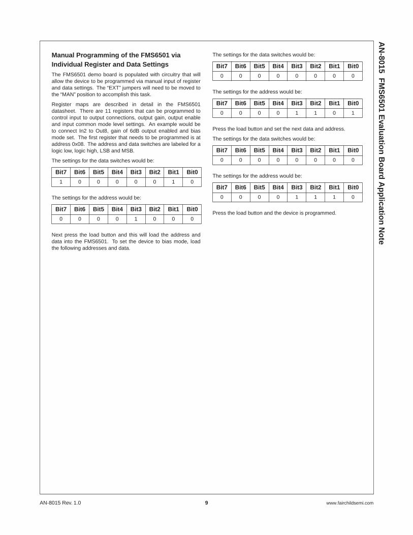
Manual Programming of the FMS6501 viaIndividual Register and Data Settings
The FMS6501 demo board is populated with circuitry that willallow the device to be programmed via manual input of registerand data settings. The “EXT” jumpers will need to be moved tothe “MAN” position to accomplish this task.
Register maps are described in detail in the FMS6501datasheet. There are 11 registers that can be programmed tocontrol input to output connections, output gain, output enableand input common mode level settings. An example would beto connect In2 to Out8, gain of 6dB output enabled and biasmode set. The first register that needs to be programmed is ataddress 0x08. The address and data switches are labeled for alogic low, logic high, LSB and MSB.
The settings for the data switches would be:
The settings for the address would be:
Next press the load button and this will load the address anddata into the FMS6501. To set the device to bias mode, loadthe following addresses and data.
The settings for the data switches would be:
The settings for the address would be:
Press the load button and set the next data and address.
The settings for the data switches would be:
The settings for the address would be:
Press the load button and the device is programmed.
Bit7 Bit6 Bit5 Bit4 Bit3 Bit2 Bit1 Bit0
1 0 0 0 0 0 1 0
Bit7 Bit6 Bit5 Bit4 Bit3 Bit2 Bit1 Bit0
0 0 0 0 1 0 0 0
Bit7 Bit6 Bit5 Bit4 Bit3 Bit2 Bit1 Bit0
0 0 0 0 0 0 0 0
Bit7 Bit6 Bit5 Bit4 Bit3 Bit2 Bit1 Bit0
0 0 0 0 1 1 0 1
Bit7 Bit6 Bit5 Bit4 Bit3 Bit2 Bit1 Bit0
0 0 0 0 0 0 0 0
Bit7 Bit6 Bit5 Bit4 Bit3 Bit2 Bit1 Bit0
0 0 0 0 1 1 1 0
AN-8015 Rev. 1.0
10
www.fairchildsemi.com
AN
-8015 FM
S6501 E
valuatio
n B
oard
Ap
plicatio
n N
ote
DISCLAIMER
FAIRCHILD SEMICONDUCTOR RESERVES THE RIGHT TO MAKE CHANGES WITHOUT FURTHER NOTICE TO ANYPRODUCTS HEREIN TO IMPROVE RELIABILITY, FUNCTION OR DESIGN. FAIRCHILD DOES NOT ASSUME ANY LIABILITYARISING OUT OF THE APPLICATION OR USE OF ANY PRODUCT OR CIRCUIT DESCRIBED HEREIN; NEITHER DOES ITCONVEY ANY LICENSE UNDER ITS PATENT RIGHTS, NOR THE RIGHTS OF OTHERS.
LIFE SUPPORT POLICY
FAIRCHILD’S PRODUCTS ARE NOT AUTHORIZED FOR USE AS CRITICAL COMPONENTS IN LIFE SUPPORTDEVICES OR SYSTEMS WITHOUT THE EXPRESS WRITTEN APPROVAL OF FAIRCHILD SEMICONDUCTOR CORPORATION.As used herein:1. Life support devices or systems are devices orsystems which, (a) are intended for surgical implant intothe body, or (b) support or sustain life, or (c) whosefailure to perform when properly used in accordancewith instructions for use provided in the labeling, can bereasonably expected to result in significant injury to theuser.
2. A critical component is any component of a lifesupport device or system whose failure to perform canbe reasonably expected to cause the failure of the lifesupport device or system, or to affect its safety oreffectiveness.
www.onsemi.com1
ON Semiconductor and are trademarks of Semiconductor Components Industries, LLC dba ON Semiconductor or its subsidiaries in the United States and/or other countries.ON Semiconductor owns the rights to a number of patents, trademarks, copyrights, trade secrets, and other intellectual property. A listing of ON Semiconductor’s product/patentcoverage may be accessed at www.onsemi.com/site/pdf/Patent−Marking.pdf. ON Semiconductor reserves the right to make changes without further notice to any products herein.ON Semiconductor makes no warranty, representation or guarantee regarding the suitability of its products for any particular purpose, nor does ON Semiconductor assume any liabilityarising out of the application or use of any product or circuit, and specifically disclaims any and all liability, including without limitation special, consequential or incidental damages.Buyer is responsible for its products and applications using ON Semiconductor products, including compliance with all laws, regulations and safety requirements or standards,regardless of any support or applications information provided by ON Semiconductor. “Typical” parameters which may be provided in ON Semiconductor data sheets and/orspecifications can and do vary in different applications and actual performance may vary over time. All operating parameters, including “Typicals” must be validated for each customerapplication by customer’s technical experts. ON Semiconductor does not convey any license under its patent rights nor the rights of others. ON Semiconductor products are notdesigned, intended, or authorized for use as a critical component in life support systems or any FDA Class 3 medical devices or medical devices with a same or similar classificationin a foreign jurisdiction or any devices intended for implantation in the human body. Should Buyer purchase or use ON Semiconductor products for any such unintended or unauthorizedapplication, Buyer shall indemnify and hold ON Semiconductor and its officers, employees, subsidiaries, affiliates, and distributors harmless against all claims, costs, damages, andexpenses, and reasonable attorney fees arising out of, directly or indirectly, any claim of personal injury or death associated with such unintended or unauthorized use, even if suchclaim alleges that ON Semiconductor was negligent regarding the design or manufacture of the part. ON Semiconductor is an Equal Opportunity/Affirmative Action Employer. Thisliterature is subject to all applicable copyright laws and is not for resale in any manner.
PUBLICATION ORDERING INFORMATIONN. American Technical Support: 800−282−9855 Toll FreeUSA/Canada
Europe, Middle East and Africa Technical Support:Phone: 421 33 790 2910
Japan Customer Focus CenterPhone: 81−3−5817−1050
www.onsemi.com
LITERATURE FULFILLMENT:Literature Distribution Center for ON Semiconductor19521 E. 32nd Pkwy, Aurora, Colorado 80011 USAPhone: 303−675−2175 or 800−344−3860 Toll Free USA/CanadaFax: 303−675−2176 or 800−344−3867 Toll Free USA/CanadaEmail: [email protected]
ON Semiconductor Website: www.onsemi.com
Order Literature: http://www.onsemi.com/orderlit
For additional information, please contact your localSales Representative
© Semiconductor Components Industries, LLC