amp display inc · this is a color active matrix tft-lcd that uses amorphous silicon tft as a...
TRANSCRIPT

Date : 2009/3/17 1
CUSTOMER
CUSTOMER PART NO.
AMPIRE PART NO. AM-640480GBTNQW-02H
APPROVED BY
DATE
Approved For Specifications Approved For Specifications & Sample
APPROVED BY CHECKED BY ORGANIZED BY
AMP DISPLAY INC.
SPECIFICATIONS
9856 SIXTH STREET RANCHO CUCAMONGA CA 91730 TEL: 909-980-13410 FAX: 909-980-1419
WWW.AMPDISPLAY.COM
AMP DISPLAY INC
Date: 2012/12/05 2
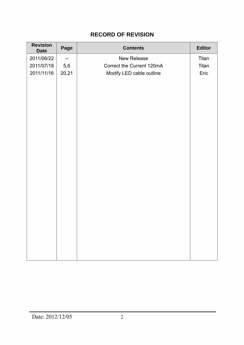
RECORD OF REVISION
Revision Date
Page Contents Editor
2011/06/22
2011/07/18
2011/11/16
--
5,6
20,21
New Release
Correct the Current 120mA
Modify LED cable outline
Titan
Titan
Eric

Date: 2012/12/05 3
1. INTRODUCTION
This is a color active matrix TFT-LCD that uses amorphous silicon TFT as a
switching device . This model is composed of a 5.7inch TFT-LCD panel, a driving
circuit. This TFT-LCD has a high resolution (640(R.G.B) X 480) and can display up to
262,144 colors .
1-1. Features
VGA Resolution
6 Bits color driver with 1 channel TTL interface
Wide range operation temperature
Improved inner FPC material to better reliability.
2. PHYSICAL SPECIFICATIONS
Item Specifications unit
Display resolution(dot) 640RGB (W) x 480(H) dots
Display area 115.2 (W) x 86.4 (H) mm
Pixel pitch 0.18 (W) x 0.18 (H) mm
Color configuration R.G.B Vertical stripe
Overall dimension 127.0(W)x99.63(H)x9.26(D) mm
Surface treatment Antiglare , Hard-Coating(3H)
Brightness 1000 cd/m2
Contrast ratio 600 : 1
Backlight unit LED
Display color 262,144 colors
Viewing Direction 6 o’clock (Gray Inversion)
Display Mode Normally White
Date: 2012/12/05 4
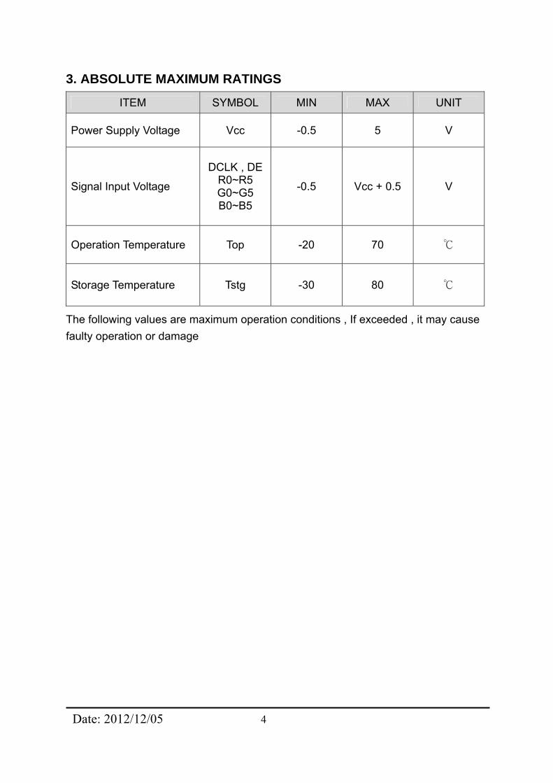
3. ABSOLUTE MAXIMUM RATINGS
ITEM SYMBOL MIN MAX UNIT
Power Supply Voltage Vcc -0.5 5 V
Signal Input Voltage
DCLK , DE R0~R5 G0~G5 B0~B5
-0.5 Vcc + 0.5 V
Operation Temperature Top -20 70
Storage Temperature Tstg -30 80
The following values are maximum operation conditions , If exceeded , it may cause
faulty operation or damage

4. ELECTRICAL CHARACTERISTICS
4-1 TFT LCD Module voltage
ITEM SYMBOL MIN TYP MAX UNIT NOTE
Power Voltage For LCD VCC 3.0 3.3 3.6 V
VIH VCC*0.
7 -- VCC V
VIL 0 -- VCC*0.
3 V Logic Input Voltage
VIL GND -- 0.3 V
4-2 LED B ht Conditacklig ions
ITEM MIN TYP MAXSYMBOL UNIT NOTE
LED Backlight Voltage VBL 17.4 19.2 21.6 V
LED Backlight Current I T BL - 120 - mA a=25LED Life Time 30K Hr Note*
Note*:Brightness to be decreased to 50% of the initial value.
LED_A
LED_K
120mA
40m
A
Date: 2012/12/05 5
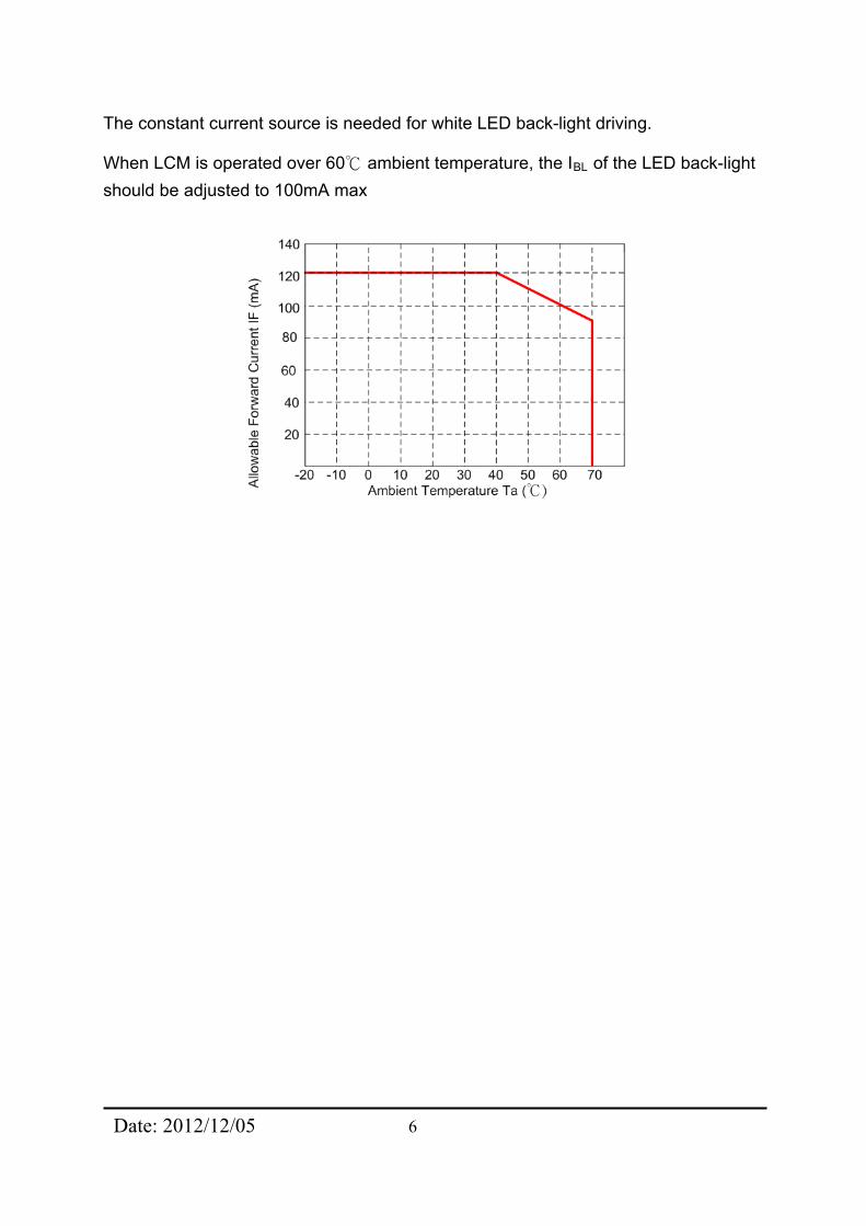
The constant current source is needed for white LED back-light driving.
When LCM is operated over 60 ambient temperature, the IBL of the LED back-light
should be adjusted to 100mA max
Date: 2012/12/05 6

Date: 2012/12/05 7
5. INTERFACE
Pin No Symbol Function 1 U/D Up or Down Display Control 2 DMS(NC) No connection 3 Hsync(NC) Honizontal SYNC. (Sync mode used) 4 VLED No connection 5 VLED No connection 6 VLED No connection 7 Vcc Power Supply for LCD 8 Vsync(NC) Vertical SYNC. (Sync mode used) 9 DE Data Enable
10 Vss Power Ground 11 Vss Power Ground 12 ADJ No connection 13 B5 Blue Data 5 (MSB) 14 B4 Blue Data 4 15 B3 Blue Data 3 16 Vss Power Ground 17 B2 Blue Data 2 18 B1 Blue Data 1 19 B0 Blue Data 0 (LSB) 20 Vss Power Ground 21 G5 Green Data 5 (MSB) 22 G4 Green Data 4 23 G3 Green Data 3 24 Vss Power Ground 25 G2 Green Data 2 26 G1 Green Data 1 27 G0 Green Data 0 (LSB) 28 Vss Power Ground 29 R5 Red Data 5 (MSB) 30 R4 Red Data 4 31 R3 Red Data 3 32 Vss Power Ground 33 R2 Red Data 2 34 R1 Red Data 1 35 R0 Red Data 0 (LSB) 36 Vss Power Ground 37 Vss Power Ground 38 DCLK Clock Signals 39 Vss Power Ground 40 L/R Left or Right Display Control
NOTE: 1. VSS Pin must ground contact, can not be floating.

Date: 2012/12/05 8
2. U/D and L/R are controlled function
L/R U/D Function
1 0 Normally display
0 0 Left and Right opposite
1 1 Up and Down opposite
0 1 Left and Right opposite , Up and Down opposite
Date: 2011/12/05 9
6. INPUT SIGNAL
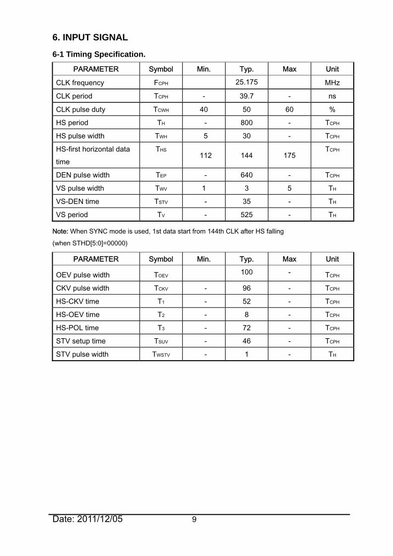
6-1 Timing Specification.
PARAMETER Symbol Min. Typ. Max Unit CLK frequency FCPH 25.175 MHz
CLK period TCPH - 39.7 - ns
CLK pulse duty TCWH 40 50 60 %
HS period TH - 800 - TCPH
HS pulse width TWH 5 30 - TCPH
HS-first horizontal data time
THS 112 144 175
TCPH
DEN pulse width TEP - 640 - TCPH
VS pulse width TWV 1 3 5 TH
VS-DEN time TSTV - 35 - TH
VS period TV - 525 - TH
Note: When SYNC mode is used, 1st data start from 144th CLK after HS falling
(when STHD[5:0]=00000)
PARAMETER Symbol Min. Typ. Max Unit
OEV pulse width TOEV 100 - TCPH CKV pulse width TCKV - 96 - TCPH
HS-CKV time T1 - 52 - TCPH
HS-OEV time T2 - 8 - TCPH
HS-POL time T3 - 72 - TCPH
STV setup time TSUV - 46 - TCPH
STV pulse width TWSTV - 1 - TH
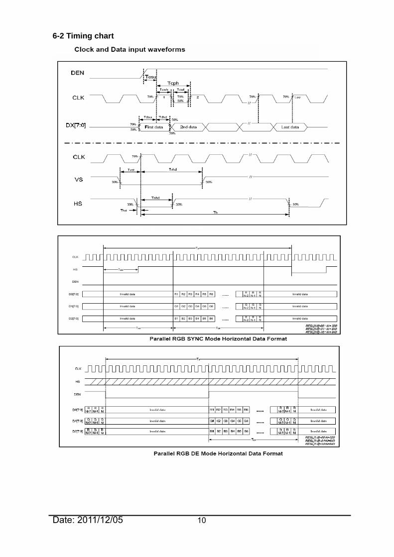
6-2 Timing chart
Date: 2011/12/05 10

Date: 2011/12/05 11
6-3 Color Data Assignment
R DATA G DATA B DATA COLOR
Input
Data R5 MSB R4 R3 R2 R1
R0LSB
G5MSB G4 G3 G2 G1
G0LSB
B5 MSB B4 B3 B2 B1
B0LSB
BLACK 0 0 0 0 0 0 0 0 0 0 0 0 0 0 0 0 0 0
RED(63) 1 1 1 1 1 1 0 0 0 0 0 0 0 0 0 0 0 0
GREEN(63) 0 0 0 0 0 0 1 1 1 1 1 1 0 0 0 0 0 0
BLUE(63) 0 0 0 0 0 0 0 0 0 0 0 0 1 1 1 1 1 1
CYAN 0 0 0 0 0 0 1 1 1 1 1 1 1 1 1 1 1 1
MAGENTA 1 1 1 1 1 1 0 0 0 0 0 0 1 1 1 1 1 1
YELLOW 1 1 1 1 1 1 1 1 1 1 1 1 0 0 0 0 0 0
BASIC
COLOR
WHITE 1 1 1 1 1 1 1 1 1 1 1 1 1 1 1 1 1 1
RED(0) 0 0 0 0 0 0 0 0 0 0 0 0 0 0 0 0 0 0
RED(1) 0 0 0 0 0 1 0 0 0 0 0 0 0 0 0 0 0 0
RED(2) 0 0 0 0 1 0 0 0 0 0 0 0 0 0 0 0 0 0
∣
RED(62) 1 1 1 1 1 0 0 0 0 0 0 0 0 0 0 0 0 0
RED
RED(63) 1 1 1 1 1 1 0 0 0 0 0 0 0 0 0 0 0 0
GREEN (0) 0 0 0 0 0 0 0 0 0 0 0 0 0 0 0 0 0 0
GREEN (1) 0 0 0 0 0 0 0 0 0 0 0 1 0 0 0 0 0 0
GREEN (2) 0 0 0 0 0 0 0 0 0 0 1 0 0 0 0 0 0 0
∣
GREEN (62) 0 0 0 0 0 0 1 1 1 1 1 0 0 0 0 0 0 0
GREEN
GREEN (63) 0 0 0 0 0 0 1 1 1 1 1 1 0 0 0 0 0 0
BLUE (0) 0 0 0 0 0 0 0 0 0 0 0 0 0 0 0 0 0 0
BLUE (1) 0 0 0 0 0 0 0 0 0 0 0 0 0 0 0 0 0 1
BLUE (2) 0 0 0 0 0 0 0 0 0 0 0 0 0 0 0 0 1 0
∣
BLUE (62) 0 0 0 0 0 0 0 0 0 0 0 0 0 0 0 0 0 1
BLUE
BLUE (63) 0 0 0 0 0 0 0 0 0 0 0 0 0 0 0 0 1 0
NOTE: (1) Definition of Gray Scale, Color (n): n is series of Gray Scale The more n value is the bright Gray Scale (2) Data: 1-High, 0-Low

7. OPTICAL CHARACTERISTICS
Item Symbol Condition Min. Typ. Max. Unit Note
Contrast ratio CR 500 600 -- -- (1)(2)(3)
Luminance Lw -- 1000 - cd/m2 (1)(3)
Luminance Uniformity ΔL 70 75 - % (1)(3)
Response Time ( White – Black )
Tr +Tf
Point - 5Θ=Φ=0°
-- 50 -- ms (1)(3)(5)
Vertical Θ 100 130 -- Viewing Angle
Horizontal Φ
CR≧10
120 150 --
Deg. (1)(2)(4)
Rx 0.566 0.616 0.666 Red
Ry 0.302 0.352 0.402
Gx 0.308 0.358 0.408 Green
Gy 0.518 0.568 0.618
Bx 0.096 0.146 0.196 Blue
By 0.086 0.136 0.186
Wx 0.279 0.329 0.379
Color chromaticity
White Wy
Point - 5Θ=Φ=0°
0.301 0.351 0.401
-- (1)(3)
NOTE:
(1) Measure conditions : 25 ± 2 , 60±10%RH under 10Lux , in the dark
room by BM-7TOPCON) ,viewing 2° , VCC=3.3V , VDD=3.3V
(2) Definition of Contrast Ratio :
Contrast Ratio (CR) = (White) Luminance of ON ÷ (Black) Luminance of
OFF
(3) Definition of Luminance : Definition of Luminance Uniformity Measure white luminance on the point 5 as figure8-1 Measure white luminance on the point 1 ~ 9 as figure8-1
ΔL = [ L(MIN) / L(MAX)] X 100%
Date: 2011/12/05 12

Figure 8-1
(4) Definition of Viewing Angle(Θ,Φ), refer to Fig8-2 as below :
Figure 8-2
(5) Definition of Response Time.(White – Black)
Date: 2011/12/05 13

Date: 2011/12/05 14
8. QUALITY AND RELIABILITY
8.1. INSPECTION QUALITY CRITERIA
8.1.1. Scope
Specifications contain 8.1.1.1 Display Quality Evaluation 8.1.1.2 Mechanics Specification
8.1.2. Sampling Plan
Unless there is other agreement, the sampling plan for incoming inspection shall follow MIL-STD-105E LEVEL II.
8.1.2.1 Lot size: Quantity per shipment as one lot (different model as different lot ). 8.1.2.2 Sampling type: Normal inspection, single sampling. 8.1.2.3 Sampling level: Level II. 8.1.2.4 AQL: Acceptable Quality Level Major defect: AQL=0.65 Minor defect: AQL=1.0
8.1.3. Panel Inspection Condition
8.1.3.1 Environment: Room Temperature: 25±5°C. Humidity: 65±5% RH. Illumination: 300 ~ 700 Lux. 8.1.3.2 Inspection Distance: 35-40 cm 8.1.3.3 Inspection Angle: The vision of inspector should be perpendicular to the surface of the Module. 8.1.3.4 Inspection time: Perceptibility Test Time: 20 seconds max.
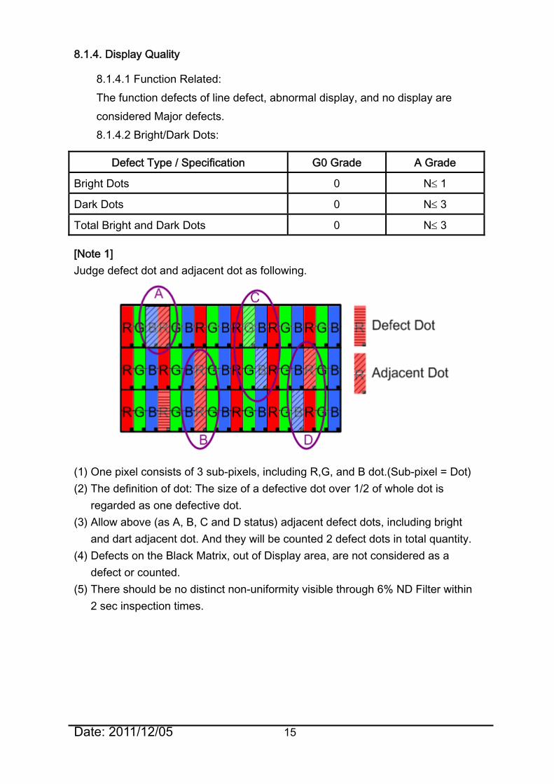
8.1.4. Display Quality
8.1.4.1 Function Related: The function defects of line defect, abnormal display, and no display are considered Major defects. 8.1.4.2 Bright/Dark Dots:
Defect Type / Specification G0 Grade A Grade
Bright Dots 0 N1
Dark Dots 0 N3
Total Bright and Dark Dots 0 N3
[Note 1] Judge defect dot and adjacent dot as following.
(1) One pixel consists of 3 sub-pixels, including R,G, and B dot.(Sub-pixel = Dot) (2) The definition of dot: The size of a defective dot over 1/2 of whole dot is
regarded as one defective dot. (3) Allow above (as A, B, C and D status) adjacent defect dots, including bright
and dart adjacent dot. And they will be counted 2 defect dots in total quantity. (4) Defects on the Black Matrix, out of Display area, are not considered as a
defect or counted. (5) There should be no distinct non-uniformity visible through 6% ND Filter within
2 sec inspection times.
Date: 2011/12/05 15
8.1.4.3 Visual Inspection specifications:
Defect Type Specification Count(N)
D0.15mm Ignored
0.15mm<D0.3mm N3
Dot Shape (Particle、Scratch and Bubbles in display area) D>0.3mm N=0
W0.05mm Ignored
0.05mm<W0.1mm,L3mm N3
Line Shape (Particles、Scratch、Lint and Bubbles in display area) W>0.1mm, L>3mm N=0
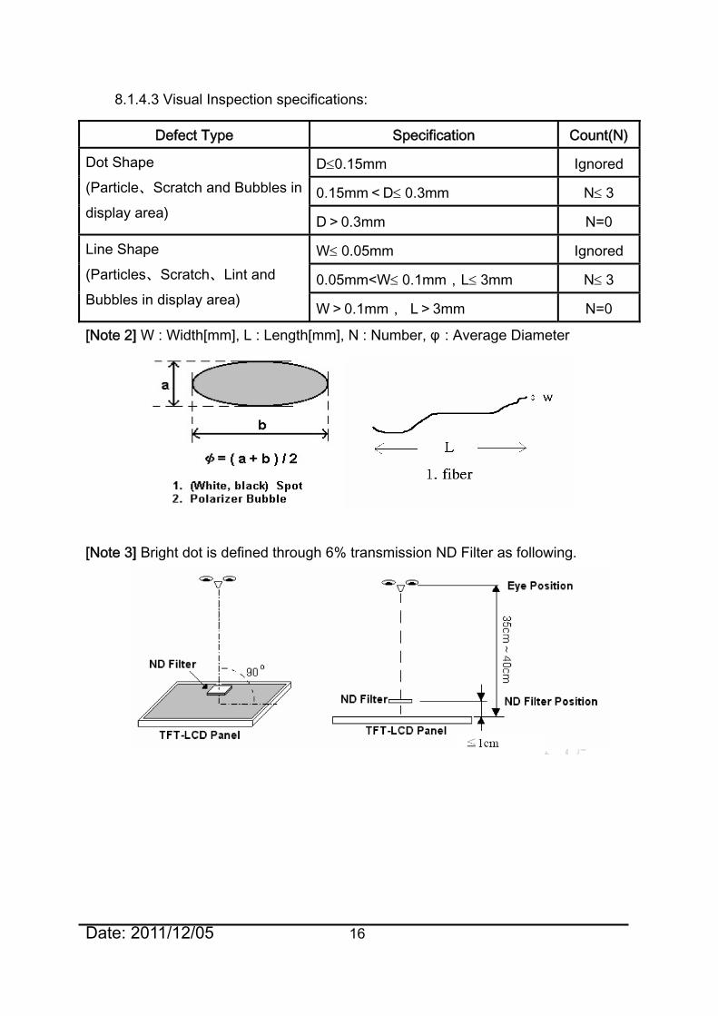
[Note 2] W : Width[mm], L : Length[mm], N : Number, φ : Average Diameter
[Note 3] Bright dot is defined through 6% transmission ND Filter as following.
Date: 2011/12/05 16

Date: 2011/12/05 17
9. RELIABILITY TEST CONDITIONS
ITEM CONDITIONS
HIGH TEMPERATURE OPERATION 70 , 240Hrs
HIGH TEMPERATURE AND HIGH HUMIDITY OPERATION
60 , 90%RH , 240Hrs
HIGH TEMPERATURE STORAGE 80 , 240Hrs
LOW TEMPERATURE OPERATION -20 , 240Hrs
LOW TEMPERATURE STORAGE -30 , 240Hrs
THERMAL SHOCK -30(0.5Hr) ~80(0.5Hr)
200Cycle

Date: 2011/12/05 18
10. USE PRECAUTIONS
10-1 Handling precautions
(1) The polarizing plate may break easily so be careful when handling it. Do not touch, press or rub it with a hard-material tool like tweezers.
(2) Do not touch the polarizing plate surface with bare hands so as not to make it dirty. If the surface or other related part of the polarizing plate is dirty, soak a soft cotton cloth or chamois leather in benzine and wipe off with it. Do not use chemical liquids such as acetone, toluene and isopropyl alcohol. Failure to do so may bring chemical reaction phenomena and deteriorations.
(3) Remove any spit or water immediately. If it is left for hours, the suffered part may deform or decolorize.
(4) If the LCD element breaks and any LC stuff leaks, do not suck or lick it. Also if LC stuff is stuck on your skin or clothing, wash thoroughly with soap and water immediately.
10-2 Installing precautions
(1) The PCB has many ICs that may be damaged easily by static electricity. To prevent breaking by static electricity from the human body and clothing, earth the human body properly using the high resistance and discharge static electricity during the operation. In this case, however, the resistance value should be approx. 1MΩ and the resistance should be placed near the human body rather than the ground surface. When the indoor space is dry, static electricity may occur easily so be careful. We recommend the indoor space should be kept with humidity of 60% or more. When a soldering iron or other similar tool is used for assembly, be sure to earth it.
(2) When installing the module and ICs, do not bend or twist them. Failure to do so may crack LC element and cause circuit failure.
(3) To protect LC element, especially polarizing plate, use a transparent protective plate (e.g., acrylic plate, glass etc) for the product case.
(4) Do not use an adhesive like a both-side adhesive tape to make LCD surface (polarizing plate) and product case stick together. Failure to do so may cause the polarizing plate to peel off
10-3 Storage precautions
(1) Avoid a high temperature and humidity area. Keep the temperature between 0°C and 35°C and also the humidity under 60%.
(2) Choose the dark spaces where the product is not exposed to direct sunlight or fluorescent light.
(3) Store the products as they are put in the boxes provided from us or in the same conditions as we recommend.

Date: 2011/12/05 19
10-4 Operating precautions
(1) Do not boost the applied drive voltage abnormally. Failure to do so may break ICs. When applying power voltage, check the electrical features beforehand and be careful. Always turn off the power to the LC module controller before removing or inserting the LC module input connector. If the input connector is removed or inserted while the power is turned on, the LC module internal circuit may break.
(2) The display response may be late if the operating temperature is under the normal standard, and the display may be out of order if it is above the normal standard. But this is not a failure; this will be restored if it is within the normal standard.
(3) The LCD contrast varies depending on the visual angle, ambient temperature, power voltage etc. Obtain the optimum contrast by adjusting the LC dive voltage.
(4) When carrying out the test, do not take the module out of the low-temperature space suddenly. Failure to do so will cause the module condensing, leading to malfunctions.
(5) Make certain that each signal noise level is within the standard (L level: 0.2Vdd or less and H level: 0.8Vdd or more) even if the module has functioned properly. If it is beyond the standard, the module may often malfunction. In addition, always connect the module when making noise level measurements.
(6) The CMOS ICs are incorporated in the module and the pull-up and pull-down function is not adopted for the input so avoid putting the input signal open while the power is ON.
(7) The characteristic of the semiconductor element changes when it is exposed to light emissions, therefore ICs on the LCD may malfunction if they receive light emissions. To prevent these malfunctions, design and assemble ICs so that they are shielded from light emissions.
(8) Crosstalk occurs because of characteristics of the LCD. In general, crosstalk occurs when the regularized display is maintained. Also, crosstalk is affected by the LC drive voltage. Design the contents of the display, considering crosstalk.
10-5 Other
(1) Do not disassemble or take the LC module into pieces. The LC modules once disassembled or taken into pieces are not the guarantee articles.
(2) The residual image may exist if the same display pattern is shown for hours. This residual image, however, disappears when another display pattern is shown or the drive is interrupted and left for a while. But this is not a problem on reliability.
(3) AMIPRE will provide one year warrantee for all products and three months warrantee for all repairing products..

11. OUTLINE DIMENSION
Date: 2011/12/05 20

Date: 2011/12/05 21