alternatives to cross-sectional sample preparation for ... · alternatives to cross-sectional...
TRANSCRIPT

Microelectronic Failure Analysis Desk Reference 2001 Supplement. Copyright © 2001. ASM International®
ALTERNATIVES TO CROSS-SECTIONAL SAMPLE PREPARATION FOR PACKAGE AND BOARD-LEVEL FAILURE ANALYSIS
Roger J. Stierman and Charles A. Odegard
DSPS Packaging Development Texas Instruments
ABSTRACT Cross sectioning plays a central role in failure analysis within the semiconductor industry. A well prepared cross section often provides physical evidence of the failure mode and fail site isolation that may or may not have been suspected from nondestructive methods such as x-ray analysis, scanning acoustic microscopy, and time domain reflectometry. In many cases, information derived from a cross section is adequate for determining the root cause leading to failure. In addition to its usefulness in failure analysis, cross sectioning also finds use as a screening technique at the package and board level (e.g., dimensional analysis of features on a package substrate). There are cases, however, in which information provided by sample preparation methods other than cross sectioning is needed to determine the root cause of failure. This paper will describe several such cases, along with recommended failure analysis (FA) approaches that serve to supplement cross sectioning for root cause analysis. INTRODUCTION Upon receiving a device for package-level failure analysis or characterization, the analyst faces an important decision in deciding which FA approach is the best to determine the root cause of failure or to properly characterize the package construction. The selected approach, which will establish the sample preparation methods and characterization tools that are used, can lead to vastly different views and information about the packaged device. There are many cases for which cross sectioning is the best approach. For
example, cross sectioning is an obvious choice for characterizing thin-film metal and interlevel dielectric (ILD) thicknesses, inspecting interfaces for evidence of nonwetting or delamination, and inspecting the bottoms of etch holes such as vias and contacts [1,2]. There are other cases, however, in which cross sectioning is not the best approach. The purpose of this paper is to highlight several alternative destructive FA approaches that can serve to supplement cross sectioning. Because the nature of the failure often dictates which approach is most appropriate, this paper will be organized according to case studies with various failure modes. These include Au-Sn embrittlement, electroless NiAu embrittlement, brittle Cu intermetallic formation, solder fatigue, and solder bridging. The alternative approaches include EDX analysis of failed interface area, parallel lapping of package substrates, dye-penetrant inspection, and surface texture analysis. Brittle Au-Sn When failures occur in Sn-containing solders on components that use Au as part of the metallization stack, the possibility for brittle Au-Sn intermetallic compounds exists. However, in these cases, problems from the intermetallic compound arise only if the Au is too thick. Because time and temperature drive intermetallic-compound formation, the limit of ‘too thick’ varies. Previous guidelines stated Au thicknesses less than 1.5 microns were ‘safe’, but in today’s applications, a better guide is Au thickness less than 0.5 microns (5000 angstroms) [11]. The root cause of Au-Sn brittleness from such low concentrations of Au (less than 1 vol. % in the solder joint) is Au migration to
© 2001 ASM International. All Rights Reserved.Microelectronic Failure Analysis Desk Reference (#09106Z)
www.asminternational.org
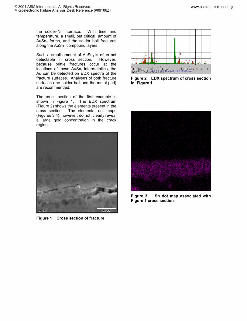
the solder-Ni interface. With time and temperature, a small, but critical, amount of AuSn4 forms, and the solder ball fractures along the AuSn4 compound layers. Such a small amount of AuSn4 is often not detectable in cross section. However, because brittle fractures occur at the locations of these AuSn4 intermetallics, the Au can be detected on EDX spectra of the fracture surfaces. Analyses of both fracture surfaces (the solder ball and the metal pad) are recommended. The cross section of the first example is shown in Figure 1. The EDX spectrum (Figure 2) shows the elements present in the cross section. The elemental dot maps (Figures 3,4), however, do not clearly reveal a large gold concentration in the crack region.
Figure 1 Cross section of fracture
Figure 2 EDX spectrum of cross section in Figure 1.
Figure 3 Sn dot map associated with Figure 1 cross section
© 2001 ASM International. All Rights Reserved.Microelectronic Failure Analysis Desk Reference (#09106Z)
www.asminternational.org

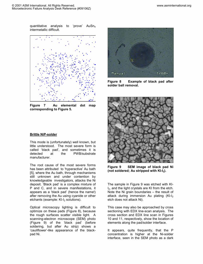
Figure 4 Au dot map associated with Figure 1 cross section An alternative approach to find the Au and brittle-fracture correlation is to examine the fracture interfaces of a failed solder ball, shown in Figure 5. Note the flat area on the substrate compared with the ‘rough’ areas around it. Sn is detected (except in the void) on the flat fractured surface and the rough parts of the fracture as shown in Figure 6. Examination of the gold dot map in Figure 7, though, shows more localized gold concentrations in the flat area. This is the signature of brittle Au-Sn failure.
Figure 5 SEM image of solder ball/pad fracture interface.
Figure 6 Sn elemental dot map corresponding to Figure 5. Sometimes the Au is detected on the fracture surface of the solder ball, sometimes on the substrate, sometimes both – therefore, for good failure analysis, both the solder ball and pad fracture surfaces must be analyzed. Detection of Au on either surface will confirm brittle Au-Sn failure as the root cause. Note that the Au signal is still small. The thin intermetallic layers (much less than the typical 1-micron penetration depth of EDX) makes
© 2001 ASM International. All Rights Reserved.Microelectronic Failure Analysis Desk Reference (#09106Z)
www.asminternational.org
quantitative analysis to ‘prove’ AuSn4 intermetallic difficult.
Figure 7 Au elemental dot map corresponding to Figure 5.
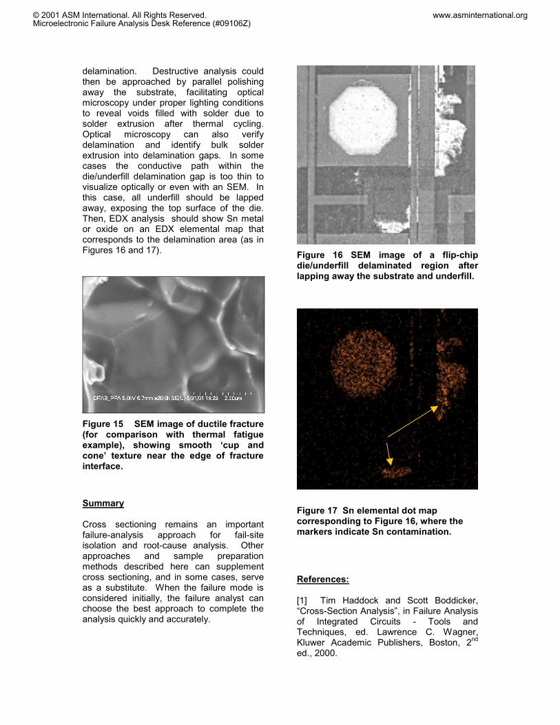
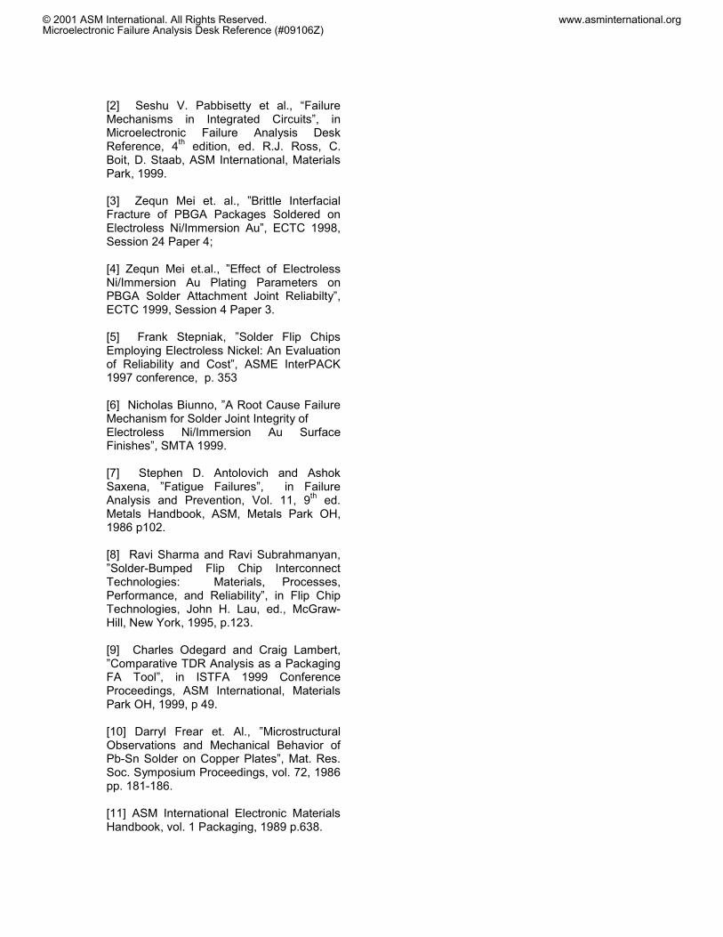
Brittle NiP-solder This mode is (unfortunately) well known, but little understood. The most severe form is called ‘black pad’, and sometimes it is detected at the PWB/substrate manufacturer. The root cause of the most severe forms has been attributed to ‘hyperactive’ Au bath [5], where the Au bath, through mechanisms still unknown and under contention by knowledgeable investigators, attacks the Ni deposit. ‘Black pad’ is a complex mixture of P and C, and in severe manifestations, it appears as a ‘black pad’ (hence the name!) after removing the Au using cyanide or other etchants (example: KI-I2 solutions). Optical microscopy lighting is difficult to optimize on these pads (Figure 8), because the rough surfaces scatter visible light. A scanning-electron microscope (SEM) photo (Figure 9) of the ‘black pad’ (before soldering, but after Au strip) shows a ‘cauliflower’-like appearance of the black-pad Ni.
Figure 8 Example of black pad after solder ball removal.
Figure 9 SEM image of black pad Ni (not soldered; Au stripped with KI-I2). The sample in Figure 9 was etched with KI-I2, and the light crystals are KI from the etch. Note the Ni grain boundaries – the result of attack during immersion Au plating (KI-I2 etch does not attack Ni). This case may also be approached by cross sectioning with EDX line-scan analysis. The cross section and EDX line scan in Figures 10 and 11, respectively, show the location of elements along the pad/solder interface. It appears, quite frequently, that the P concentration is higher at the Ni-solder interface, seen in the SEM photo as a dark
© 2001 ASM International. All Rights Reserved.Microelectronic Failure Analysis Desk Reference (#09106Z)
www.asminternational.org

line. It is also noted that there is a significant buildup of P in the solder above this interface, significantly higher in the solder than the X-ray count background. The reason is not yet understood, but it is theorized that buildup of P occurs in the Au during Au deposition (from excess replacement reaction of Ni by Au). Then, during solder reflow, the P does not mix in the solder (when the Au dissolves), but tends to agglomerate near the Ni surface. Given enough time and temperature, P can react with Ni to form brittle Ni3P intermetallic compound.
Figure 10. Cross section of solder/pad interface. If this theory has validity, then controls that prevent Au hyperactivity on Ni – such as processes that slow Au deposition or less-active Au baths - will minimize P buildup and thereby delay Ni3P formation over useful product lifetimes. The best-understood method for slowing Au deposition is to use an Ni-P alloy with high P content (11-13 wt. % P). There are reports of critical solder applications using high-P alloys that do not exhibit brittle failures [5].
0
200
400
600
800
1000
1200
1400
1 5 9 13 17 21 25 29 33 37 41 45 49 53 57 61 65 69 73 77 81 85 89 93 97 101
105
109
113
117
121
125
Relative Position
Cou
nts/
sec.
PNiCuSnPb
Figure 11 EDX spectrum corresponding to Figure 10. Note slight peak in P at Ni-solder border. There does appear to be some latency time involved with this P [3, 4, 6]. This can also explain why some packages (or even pads on the same packages) can test good when others fail miserably. The quest for this theory (or its replacement) continues. Brittle Cu intermetallic failure This has occurred infrequently, but deserves some mention. In this case, the solder ball is attached to a Cu/OSP substrate, yet it had a brittle ball failure as shown in Figure 12.
Figure 12 Fracture at Cu(OSP)/Solder interface. It appears that the fracture occurred in the Cu-Sn intermetallic region. One clue is that the intermetallics are rather thin (less than 1 micron total thickness). This is much
© 2001 ASM International. All Rights Reserved.Microelectronic Failure Analysis Desk Reference (#09106Z)
www.asminternational.org

thinner than one should expect from most furnace soldering profiles. However, there is a distinct Cu-Sn intermetallic layer, and it appears uniform, so soldering did occur (this is not a non-wet). From the phase diagram, the first compound that forms between Sn and Cu is Cu3Sn, a very brittle intermetallic that tends to form at the Cu surface [10]. The equilibrium compound, Cu6Sn5, has greater strength. This failure was, therefore, ascribed to insufficient solder reflow time. A slightly longer time above reflow temperature (10-15 seconds additional) was suggested. The preceding three cases illustrate the various FA approaches that can be used to determine solder balloff failure modes. Selecting the best approach will facilitate failure analysis in a manner that collects maximum information without prematurely contaminating the sample from further analyses. An outline of FA approaches, in summary, is as follows: Ni-Au metallized substrates: 0) Is there Au, or lack of Sn, on the pad
surface? (Yes = non-wet. Analyze by FTIR first, scanning Auger second).
1) Is Au detected on either of the fracture surfaces? Does it correlate with flat fracture areas? (Yes, then Au-Sn embrittlement).
2) Is there a buildup of P at the Ni-solder interface? (Yes, then suspect hyperactive Au bath).
Cu-OSP substrates: 0) Is there Sn on the surface? (No, then
probably a non-wet. Analyze FTIR & troubleshoot OSP).
1) If Sn on surface = Yes, then compare thickness & quantitative analysis of layer – Cu3Sn is much more brittle than Cu6Sn5, and longer reflow time may be needed.
Solder Thermal Fatigue Open-circuit failure due to solder thermal fatigue can occur when a solder connection,
such as a flip-chip bump or ball-grid-array (BGA) solder ball, experiences temperature cycling [7]. Fatigue crack initiation and growth occur over the operating life as the device is turned on and off, where the device heats up and consequently experiences thermal stress (due to coefficient of thermal expansion (CTE) mismatch of package materials) with each on/off cycle. Environmental tests such as thermal cycling are performed during package development to establish whether or not the device will survive the desired life span before failing by solder thermal fatigue. At the package level, thermal fatigue is becoming a less common failure mode. This is due to improvements in underfill-to-die adhesion, resulting in fewer cases of delamination and therefore uniform distribution of packaging stress over the entire die/underfill interface area [8]. At the board level, however, underfill is typically not used between the package and the PCB around the BGA solder balls to minimize assembly costs. Thermal stress is, therefore, concentrated at the BGA solder-ball connections. Because solder fatigue is inevitable under cyclic loading, time to failure is assessed by thermal cycle testing of the board assembly. No nondestructive technique has yet been shown to identify all solder fatigue failure sites for a BGA array. X-ray and scanning-acoustic microscopy (SAM) analyses are obscured by the numerous metal, organic, and/or oxide layers of the package and board assemblies. Time domain reflectometry can be an effective tool for this case [9], but it may be limited to test boards with isolated paths to each BGA connection (rather than functional board assemblies with multiple pin connections and branched path connections). Cross-sectional analysis is a possible approach for solder-fatigue failure-site isolation. However, this can be a very tedious task when attempting to inspect all BGA solder ball connections (typically in the range of tens to hundreds of BGA ball connections). In this approach, a row of solder balls is cross sectioned, inspected, and documented, and then the process is repeated until every solder ball row has
© 2001 ASM International. All Rights Reserved.Microelectronic Failure Analysis Desk Reference (#09106Z)
www.asminternational.org

been sectioned. A better approach is one that would facilitate fast inspection of all BGA connections for evidence of complete or partial solder fatigue cracks. One alternative approach is dye penetrant inspection. The first step involves saturating the interconnect region between the package and board with liquid dye penetrant. This is achieved by submersing the entire board assembly into a container filled with liquid dye penetrant. The container is then placed in a sealed vacuum chamber and then evacuated with a floor pump. This step draws air out of the small gaps and cracks that may exist within the solder. After a few minutes the vacuum is released, forcing the liquid dye penetrate to backfill into evacuated gaps and cracks. The board assembly is then removed from the container of liquid dye penetrant and heated on a hot plate to dry the dye penetrant. After the dye penetrant has dried, the package is pried away from the board. The exposed package and board are inspected for evidence of solder cracks wherever dye penetrant is found within a fracture surface area of solder. Another approach is to inspect fracture surfaces for striations. Striations are finely spaced parallel marks on the solder fracture surface resulting from fatigue crack propagation with each thermal cycle [41]. In this approach, the package is simply pried away from the board and inspected for striations under high magnification SEM. Figure 13 and 14 show striations at the fracture surface edge and center, respectively, of a thermal fatigue failure. Figure 15 shows an example of a ductile fracture (not thermally fatigued) of a different unit (but the same device type) as a comparison. Another approach would be EDX inspection, which would show solder on both sides of fracture interface. Note that the x-ray activation volume is about a micron at typical accelerating-voltage setting of 25 keV, so fractures within about a micron of the pad may show pad metallurgy in the spectrum.
Figure 13 SEM image of solder thermal fatigue fractured interface showing striations near the edge of fracture interface.
Figure 14 SEM image of solder thermal fatigue fractured interface showing striations near the center of fracture interface. Solder Bridging Solder bridging in flip-chip devices results in electrical short and/or leakage failures. Two scenarios that can lead to solder bridging include 1) presence of underfill voids that fill by solder extrusion after thermal cycling and 2) presence of delamination at the die/underfill interface, which allows a conductive path of solder metal thin film across die surface. A preliminary nondestructive approach would be scanning acoustic microscopy inspection, where we expect to see voids or
© 2001 ASM International. All Rights Reserved.Microelectronic Failure Analysis Desk Reference (#09106Z)
www.asminternational.org
delamination. Destructive analysis could then be approached by parallel polishing away the substrate, facilitating optical microscopy under proper lighting conditions to reveal voids filled with solder due to solder extrusion after thermal cycling. Optical microscopy can also verify delamination and identify bulk solder extrusion into delamination gaps. In some cases the conductive path within the die/underfill delamination gap is too thin to visualize optically or even with an SEM. In this case, all underfill should be lapped away, exposing the top surface of the die. Then, EDX analysis should show Sn metal or oxide on an EDX elemental map that corresponds to the delamination area (as in Figures 16 and 17).
Figure 15 SEM image of ductile fracture (for comparison with thermal fatigue example), showing smooth ‘cup and cone’ texture near the edge of fracture interface. Summary Cross sectioning remains an important failure-analysis approach for fail-site isolation and root-cause analysis. Other approaches and sample preparation methods described here can supplement cross sectioning, and in some cases, serve as a substitute. When the failure mode is considered initially, the failure analyst can choose the best approach to complete the analysis quickly and accurately.
Figure 16 SEM image of a flip-chip die/underfill delaminated region after lapping away the substrate and underfill.
Figure 17 Sn elemental dot map corresponding to Figure 16, where the markers indicate Sn contamination. References: [1] Tim Haddock and Scott Boddicker, “Cross-Section Analysis”, in Failure Analysis of Integrated Circuits - Tools and Techniques, ed. Lawrence C. Wagner, Kluwer Academic Publishers, Boston, 2nd ed., 2000.
© 2001 ASM International. All Rights Reserved.Microelectronic Failure Analysis Desk Reference (#09106Z)
www.asminternational.org
[2] Seshu V. Pabbisetty et al., “Failure Mechanisms in Integrated Circuits”, in Microelectronic Failure Analysis Desk Reference, 4th edition, ed. R.J. Ross, C. Boit, D. Staab, ASM International, Materials Park, 1999. [3] Zequn Mei et. al., ”Brittle Interfacial Fracture of PBGA Packages Soldered on Electroless Ni/Immersion Au”, ECTC 1998, Session 24 Paper 4; [4] Zequn Mei et.al., ”Effect of Electroless Ni/Immersion Au Plating Parameters on PBGA Solder Attachment Joint Reliabilty”, ECTC 1999, Session 4 Paper 3. [5] Frank Stepniak, ”Solder Flip Chips Employing Electroless Nickel: An Evaluation of Reliability and Cost”, ASME InterPACK 1997 conference, p. 353 [6] Nicholas Biunno, ”A Root Cause Failure Mechanism for Solder Joint Integrity of Electroless Ni/Immersion Au Surface Finishes”, SMTA 1999. [7] Stephen D. Antolovich and Ashok Saxena, ”Fatigue Failures”, in Failure Analysis and Prevention, Vol. 11, 9th ed. Metals Handbook, ASM, Metals Park OH, 1986 p102. [8] Ravi Sharma and Ravi Subrahmanyan, ”Solder-Bumped Flip Chip Interconnect Technologies: Materials, Processes, Performance, and Reliability”, in Flip Chip Technologies, John H. Lau, ed., McGraw-Hill, New York, 1995, p.123. [9] Charles Odegard and Craig Lambert, ”Comparative TDR Analysis as a Packaging FA Tool”, in ISTFA 1999 Conference Proceedings, ASM International, Materials Park OH, 1999, p 49. [10] Darryl Frear et. Al., ”Microstructural Observations and Mechanical Behavior of Pb-Sn Solder on Copper Plates”, Mat. Res. Soc. Symposium Proceedings, vol. 72, 1986 pp. 181-186. [11] ASM International Electronic Materials Handbook, vol. 1 Packaging, 1989 p.638.
© 2001 ASM International. All Rights Reserved.Microelectronic Failure Analysis Desk Reference (#09106Z)
www.asminternational.org

ASM International is the society for materials engineers and scientists, a worldwide network dedicated to advancing industry, technology, and applications of metals and materials. ASM International, Materials Park, Ohio, USA www.asminternational.org
This publication is copyright © ASM International®. All rights reserved.
Publication title Product code Microelectronic Failure Analysis Desk Reference 2001 Supplement
#09106Z
To order products from ASM International:
Online Visit www.asminternational.org/bookstore
Telephone 1-800-336-5152 (US) or 1-440-338-5151 (Outside US) Fax 1-440-338-4634
Mail Customer Service, ASM International 9639 Kinsman Rd, Materials Park, Ohio 44073-0002, USA
Email [email protected]
In Europe
American Technical Publishers Ltd. 27-29 Knowl Piece, Wilbury Way, Hitchin Hertfordshire SG4 0SX, United Kingdom Telephone: 01462 437933 (account holders), 01462 431525 (credit card) www.ameritech.co.uk
In Japan Neutrino Inc. Takahashi Bldg., 44-3 Fuda 1-chome, Chofu-Shi, Tokyo 182 Japan Telephone: 81 (0) 424 84 5550
Terms of Use. This publication is being made available in PDF format as a benefit to members and customers of ASM International. You may download and print a copy of this publication for your personal use only. Other use and distribution is prohibited without the express written permission of ASM International. No warranties, express or implied, including, without limitation, warranties of merchantability or fitness for a particular purpose, are given in connection with this publication. Although this information is believed to be accurate by ASM, ASM cannot guarantee that favorable results will be obtained from the use of this publication alone. This publication is intended for use by persons having technical skill, at their sole discretion and risk. Since the conditions of product or material use are outside of ASM's control, ASM assumes no liability or obligation in connection with any use of this information. As with any material, evaluation of the material under end-use conditions prior to specification is essential. Therefore, specific testing under actual conditions is recommended. Nothing contained in this publication shall be construed as a grant of any right of manufacture, sale, use, or reproduction, in connection with any method, process, apparatus, product, composition, or system, whether or not covered by letters patent, copyright, or trademark, and nothing contained in this publication shall be construed as a defense against any alleged infringement of letters patent, copyright, or trademark, or as a defense against liability for such infringement.