aixtron investor presentation investor presentation ... in particular in the chapter risks in the...
TRANSCRIPT
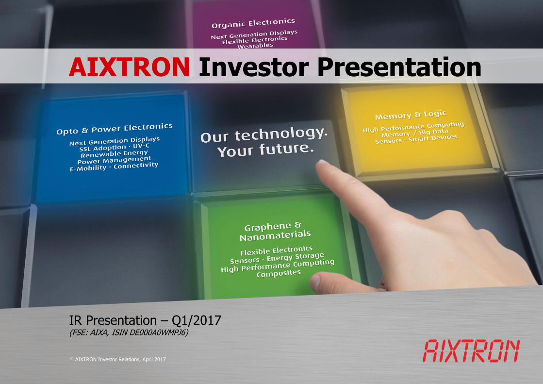
AIXTRON Investor Presentation
IR Presentation – Q1/2017(FSE: AIXA, ISIN DE000A0WMPJ6)
© AIXTRON Investor Relations, April 2017
Disclaimer 2
Forward-Looking Statements
This document may contain forward-looking statements regarding the business, results of operations, financial condition andearnings outlook of AIXTRON. These statements may be identified by words such as “may”, “will”, “expect”, “anticipate”,“contemplate”, “intend”, “plan”, “believe”, “continue” and “estimate” and variations of such words or similar expressions. Theseforward-looking statements are based on our current assessments, expectations and assumptions, of which many are beyondcontrol of AIXTRON, and are subject to risks and uncertainties. You should not place undue reliance on these forward-lookingstatements. Should these risks or uncertainties materialize, or should underlying expectations not occur or assumptions proveincorrect, actual results, performance or achievements of AIXTRON may materially vary from those described explicitly or implicitlyin the relevant forward-looking statement. This could result from a variety of factors, such as actual customer orders received byAIXTRON, the level of demand for deposition technology in the market, the timing of final acceptance of products by customers,the condition of financial markets and access to financing for AIXTRON, general conditions in the market for deposition plants andmacroeconomic conditions, cancellations, rescheduling or delays in product shipments, production capacity constraints, extendedsales and qualification cycles, difficulties in the production process, the general development in the semi-conductor industry,increased competition, fluctuations in exchange rates, availability of public funding, fluctuations and/or changes in interest rates,delays in developing and marketing new products, a deterioration of the general economic situation and any other factors discussedin any reports or other announcements , in particular in the chapter Risks in the Annual Report, filed by AIXTRON. Any forward-looking statements contained in this document are based on current expectations and projections of the executive board based oninformation available the date hereof. AIXTRON undertakes no obligation to revise or update any forward-looking statements as aresult of new information, future events or otherwise, unless expressly required to do so by law.
This document is an English language translation of a document in German language. In case of discrepancies, the Germanlanguage document shall prevail and shall be the valid version.
Due to rounding, numbers presented throughout this presentation may not add up precisely to the totals indicated and percentagesmay not precisely reflect the absolute figures for the same reason.
Our registered trademarks: AIXACT®, AIXTRON®, Atomic Level SolutionS®, Close Coupled Showerhead®, CRIUS®, Gas FoilRotation®, OVPD®, Planetary Reactor®, PVPD®, TriJet®, Optacap™
Our Vision
Technology. Materials. Performance.
Technology.
We are the recognized technology leader in complex material deposition.
Materials.
We enable our customers to successfully shape the markets of the future, exploiting the potential offered by new materials.
Performance.
We deliver the performance driving economic success through our expertise, our employees and the quality of our products.
ABOUT AIXTRON 3
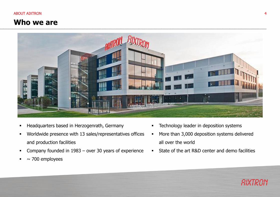
Who we are
Headquarters based in Herzogenrath, Germany
Worldwide presence with 13 sales/representatives offices
and production facilities
Company founded in 1983 – over 30 years of experience
~ 700 employees
Technology leader in deposition systems
More than 3,000 deposition systems delivered
all over the world
State of the art R&D center and demo facilities
4ABOUT AIXTRON
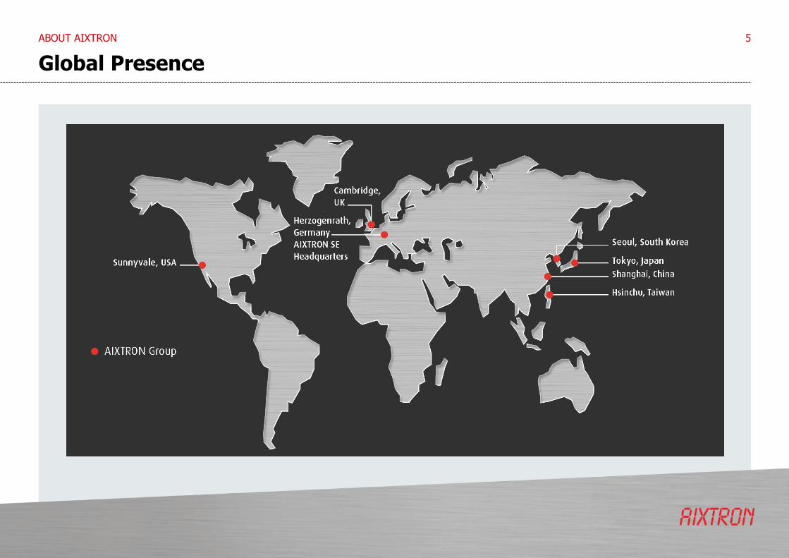
Global Presence
ABOUT AIXTRON 5
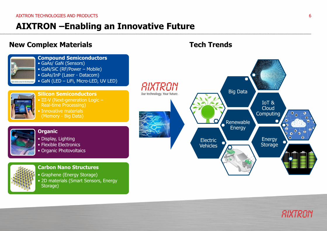
AIXTRON –Enabling an Innovative Future
AIXTRON TECHNOLOGIES AND PRODUCTS 6
Compound Semiconductors• GaAs/ GaN (Sensors)
• GaN/SiC (RF/Power – Mobile)
• GaAs/InP (Laser - Datacom)
• GaN (LED – LiFi, Micro-LED, UV LED)
Silicon Semiconductors • III-V (Next-generation Logic –
Real-time Processing)
• Innovative materials(Memory - Big Data)
Organic
• Display, Lighting
• Flexible Electronics
• Organic Photovoltaics
Carbon Nano Structures
• Graphene (Energy Storage)
• 2D materials (Smart Sensors, Energy Storage)
New Complex Materials
LOREM
LOREM
LOREM
LOREM
LOREM
Renewable Energy
IoT & Cloud
Computing
Big Data
Electric Vehicles
Energy Storage
Tech Trends

Compound Semiconductors
MOCVD ALD/CVD/MOCVD
LEDs, Lasers and
Optoelectronics
• LEDs for display:TVs, mobile phones,tablets, etc.
• LEDs for lighting
• LEDs for automotive
• LEDs for datacom
• Lasers for telecom,
consumer electronics
• Photovoltaics
Increasing demand for
Advanced Optoelectronics
Our Technology Portfolio
7
SiliconSemiconductors
• RF transistors
• AC-DC converters
• DC-DC converters
• Solar inverters
• Motor drives inindustrial applicationsautomotive andconsumer electronics
Power ManagementGaN / SiC
• DRAM Dielectric and Metal Electrode
• Flash Inter Poly Dielectric and Metals
• ReRAM and PCRAM Active element and Electrode
• Logic Gate stack
• Logic High MobilityChannel
SiliconSemiconductors
Growth in NAND Flash driving Demand
TFOS in Early Development
New Applications driving Demand
• OLEDs for display:TVs, mobile phones,tablets, etc.
• Thin Film Encapsulation
• OLEDs for lighting
• Organic, flexible electronics
• Organic Photovoltaics
• Transistors
• Interconnects
• Flexible Electronics
• Energy Storage
• Sensors, etc.
Organic ElectronicsGraphene, 2D Nano
CNTs and CNWs
OrganicCarbon
Nanomaterials
OVPD®/PVPD®/TFE PECVD
Production Qualification withRelevant Customers
Increasing equipment
demand expected by
2018 and beyond
AIXTRON TECHNOLOGIES AND PRODUCTS
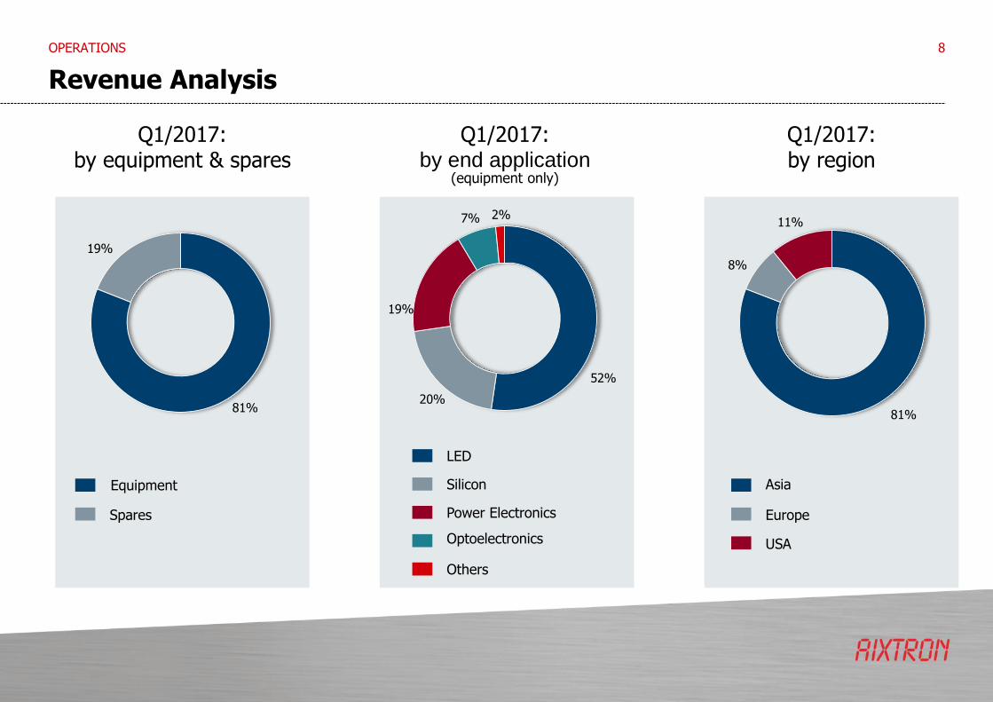
Revenue Analysis
OPERATIONS 8
Q1/2017:by region
Q1/2017:by equipment & spares
Spares
Equipment
Q1/2017:by end application
(equipment only)
USA
Europe
Asia
Power Electronics
Silicon
LED
Optoelectronics
Others
81%
19%
52%
20%
19%
7% 2%
81%
8%
11%
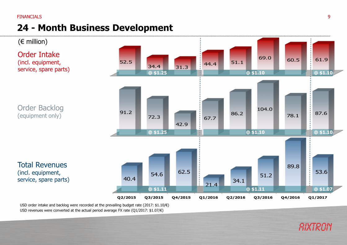
Q2/2015 Q3/2015 Q4/2015 Q1/2016 Q2/2016 Q3/2016 Q4/2016 Q1/2017
40.454.6 62.5
21.434.1
51.2
89.853.6
52.5 34.4 31.3
44.4 51.1 69.0 60.5 61.9
91.2 72.3
42.9
67.7 86.2
104.0
78.1 87.6
24 - Month Business Development
FINANCIALS 9
USD order intake and backlog were recorded at the prevailing budget rate (2017: $1.10/€)
USD revenues were converted at the actual period average FX rate (Q1/2017: $1.07/€)
@ $1.25
@ $1.25
@ $1.11
@ $1.10
@ $1.10
@ $1.11
Order Intake(incl. equipment, service, spare parts)
(€ million)
Total Revenues(incl. equipment, service, spare parts)
Order Backlog(equipment only)
@ $1.10
@ $1.10
@ $1.07
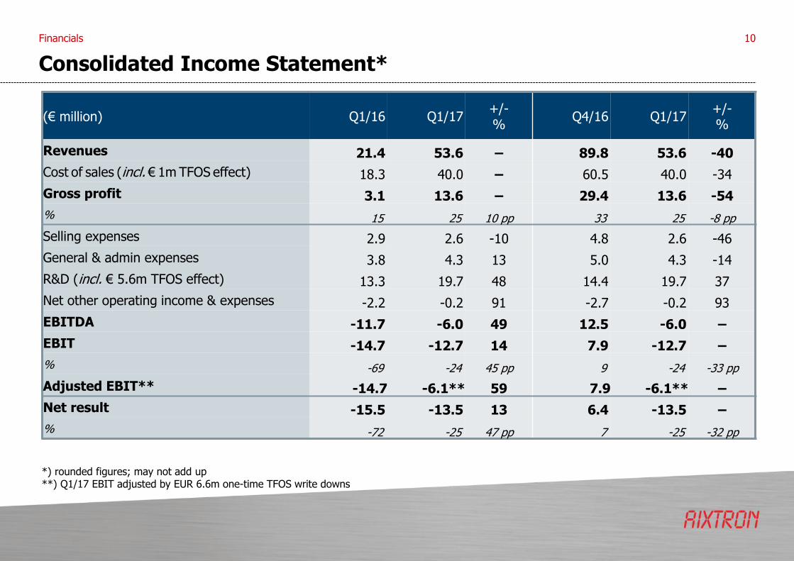
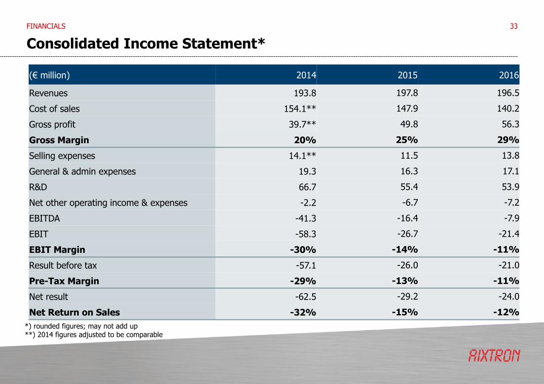
Consolidated Income Statement*
10Financials
(€ million) Q1/16 Q1/17+/-%
Q4/16 Q1/17+/-%
Revenues 21.4 53.6 – 89.8 53.6 -40
Cost of sales (incl. € 1m TFOS effect) 18.3 40.0 – 60.5 40.0 -34
Gross profit 3.1 13.6 – 29.4 13.6 -54
% 15 25 10 pp 33 25 -8 pp
Selling expenses 2.9 2.6 -10 4.8 2.6 -46
General & admin expenses 3.8 4.3 13 5.0 4.3 -14
R&D (incl. € 5.6m TFOS effect) 13.3 19.7 48 14.4 19.7 37
Net other operating income & expenses -2.2 -0.2 91 -2.7 -0.2 93
EBITDA -11.7 -6.0 49 12.5 -6.0 –
EBIT -14.7 -12.7 14 7.9 -12.7 –
% -69 -24 45 pp 9 -24 -33 pp
Adjusted EBIT** -14.7 -6.1** 59 7.9 -6.1** –
Net result -15.5 -13.5 13 6.4 -13.5 –
% -72 -25 47 pp 7 -25 -32 pp
*) rounded figures; may not add up**) Q1/17 EBIT adjusted by EUR 6.6m one-time TFOS write downs
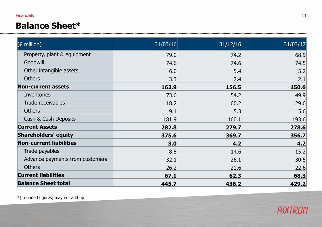
Balance Sheet*
11
*) rounded figures; may not add up
(€ million) 31/03/16 31/12/16 31/03/17
Property, plant & equipment 79.0 74.2 68.9
Goodwill 74.6 74.6 74.5
Other intangible assets 6.0 5.4 5.2
Others 3.3 2.4 2.1
Non-current assets 162.9 156.5 150.6
Inventories 73.6 54.2 49.9
Trade receivables 18.2 60.2 29.6
Others 9.1 5.3 5.6
Cash & Cash Deposits 181.9 160.1 193.6
Current Assets 282.8 279.7 278.6
Shareholders' equity 375.6 369.7 356.7
Non-current liabilities 3.0 4.2 4.2
Trade payables 8.8 14.6 15.2
Advance payments from customers 32.1 26.1 30.5
Others 26.2 21.6 22.6
Current liabilities 67.1 62.3 68.3
Balance Sheet total 445.7 436.2 429.2
Financials

Consolidated Statement of Cash Flows*
12
(€ million) Q1/16 Q1/17 Q4/16 Q1/17
Net Result-15.5 -13.5 6.4 -13.5
Adjust for
Non Cash Items 3.7 7.3 5.9 7.3
Changes in Working Capital -7.6 40.8 -15.0 40.8
Cash Flow from Operating Activities -19.4 34.6 -2.7 34.6
Capital Expenditures -5.1 -1.3 -2.2 -1.3
Financing / FX effects -2.7 0.3 1.3 0.3
Total Cash Flow (excl. Changes in Deposits) -27.2 33.6 -3.6 33.6
Cash & Deposits181.9 193.6 160.1 193.6
Financials
*) rounded figures; may not add up

Market Prospects
Short-Term• Further increasing adoption of LEDs and specialty LEDs (in particular Red-Orange-Yellow, UV or IR) for Display and other
applications
• Increased emergence of wide-band-gap GaN or SiC based devices for energy efficient power management and communications in automotive, consumer electronics and mobile applications
• Development of next generation NAND and DRAM memory devices
• Increasing emergence of compound semiconductor based laser devices for ultrafast data transfer and sensors in infrastructure and mobile applications
• Increasing emergence of compound semiconductor based sensor devices for autonomous driving
Mid- to Long-Term• Further progress in the development of GaN-on-Silicon LEDs and Wafer Level Packaging
• Development of new wide-band-gap applications such as RF and System-on-Chip with integrated power management
• Progress in the development of large area OLED devices requiring efficient deposition technologies
• Progress in the development of flexible and rigid OLED devices requiring thin-film encapsulation
• Increased development activity for specialized compound solar cell applications
• Increasing requirements for High-k and interconnect components, implying a new approach to production technologies
• Progress in the development of future logic chips applying wide band gap and high electron mobility materials (III-V-on-Silicon)
• Development of applications using Carbon Nanostructures (Carbon Nanotubes, Carbon Nanowires, Graphene)
• Development of alternative LED applications such as Visual Light Communication technology or Micro-LED Displays
FUTURE MARKETS 13
AIXTRON INVESTOR PRESENTATION 14
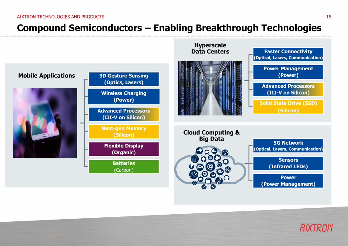
Compound Semiconductors – Enabling Breakthrough Technologies
AIXTRON TECHNOLOGIES AND PRODUCTS 15
3D Gesture Sensing
(Optics, Lasers)
Wireless Charging
(Power)
Advanced Processors
(III-V on Silicon)
Next-gen Memory
(Silicon)
Flexible Display
(Organic)
Batteries
(Carbon)
Faster Connectivity(Optical, Lasers, Communication)
Power Management
(Power)
Advanced Processors
(III-V on Silicon)
Solid State Drive (SSD)
(Silicon)
5G Network(Optical, Lasers, Communication)
Sensors
(Infrared LEDs)
Power
(Power Management)
Mobile Applications
HyperscaleData Centers
Cloud Computing & Big Data
AIXTRON – Enabling Emerging Global Mega Trends
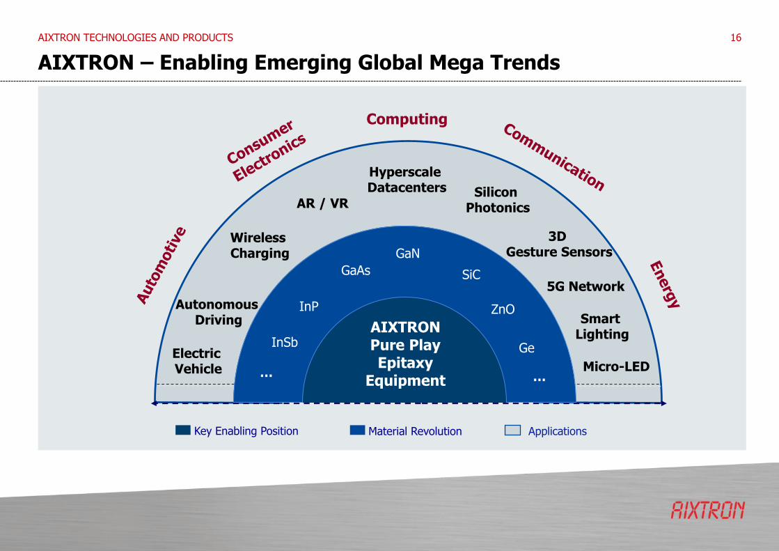
AIXTRON TECHNOLOGIES AND PRODUCTS 16
Key Enabling Position Material Revolution Applications
AIXTRONPure Play Epitaxy
Equipment
GaAs
InP
GaN
SiC
InSb
…
ZnO
Ge
…
Wireless Charging
Autonomous Driving
5G Network
Electric Vehicle
AR / VR
HyperscaleDatacenters
Smart Lighting
Micro-LED
Silicon Photonics
3D Gesture Sensors
Computing
AIXTRON – Enabling Emerging Global Mega Trends
AIXTRON TECHNOLOGIES AND PRODUCTS 17
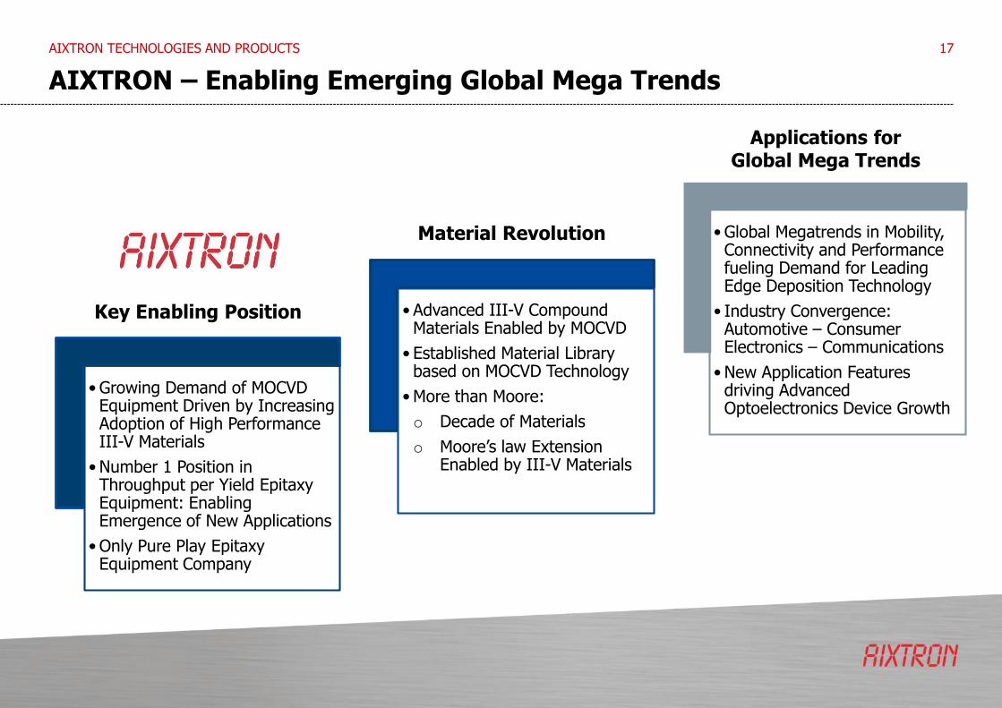
• Growing Demand of MOCVD Equipment Driven by Increasing Adoption of High Performance III-V Materials
• Number 1 Position in Throughput per Yield Epitaxy Equipment: Enabling Emergence of New Applications
• Only Pure Play Epitaxy Equipment Company
• Advanced III-V Compound Materials Enabled by MOCVD
• Established Material Library based on MOCVD Technology
• More than Moore:
o Decade of Materials
o Moore’s law Extension Enabled by III-V Materials
• Global Megatrends in Mobility, Connectivity and Performance fueling Demand for Leading Edge Deposition Technology
• Industry Convergence: Automotive – Consumer Electronics – Communications
• New Application Features driving Advanced Optoelectronics Device Growth
Key Enabling Position
Material Revolution
Applications forGlobal Mega Trends
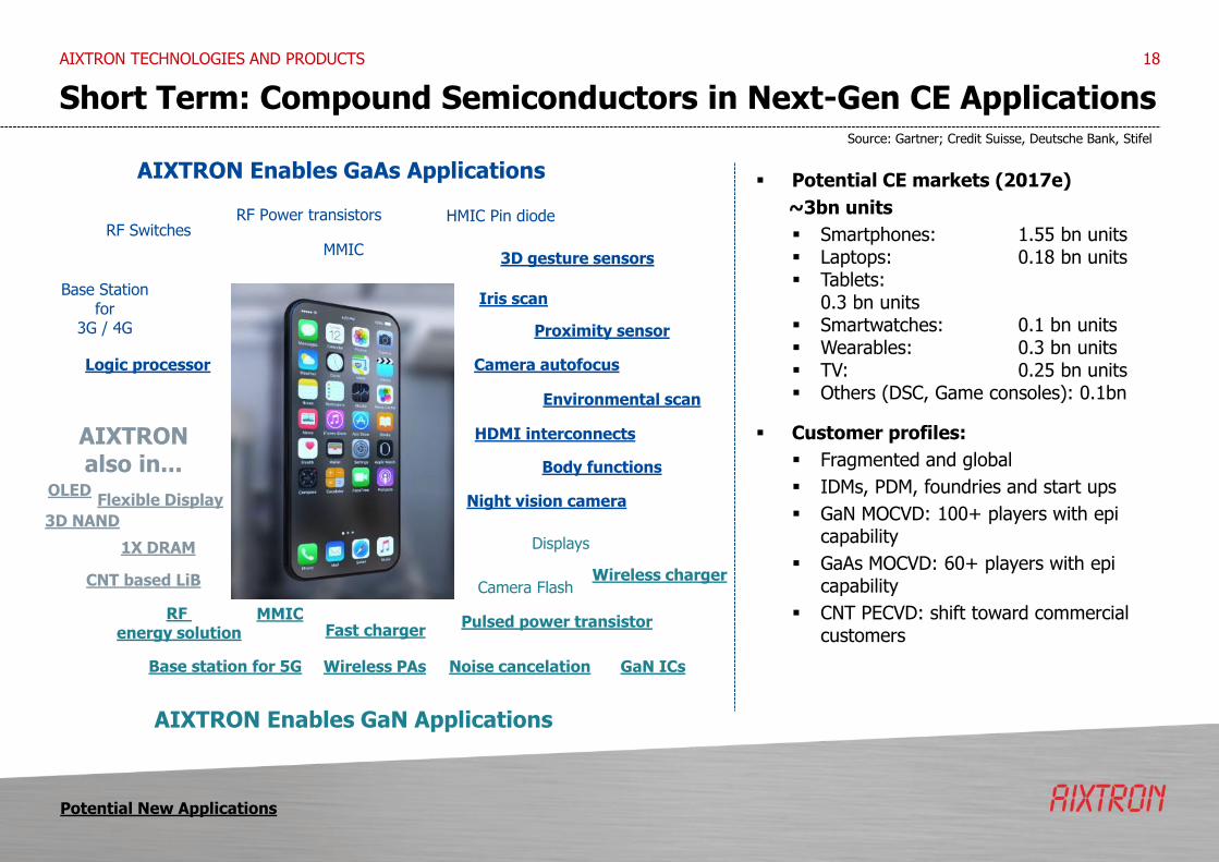
Short Term: Compound Semiconductors in Next-Gen CE Applications
AIXTRON TECHNOLOGIES AND PRODUCTS 18
AIXTRON Enables GaAs Applications
MMIC
AIXTRON Enables GaN Applications
AIXTRON also in...
RF SwitchesRF Power transistors HMIC Pin diode
Base Station for
3G / 4G
Displays
Camera Flash
OLED
Iris scan
3D gesture sensors
Proximity sensor
Camera autofocus
Environmental scan
HDMI interconnects
Body functions
Night vision camera
Logic processor
Pulsed power transistorMMICRF
energy solution
Base station for 5G
Fast charger
Wireless charger
Wireless PAs Noise cancelation GaN ICs
3D NAND
1X DRAM
CNT based LiB
Flexible Display
Potential CE markets (2017e)
~3bn units
Smartphones: 1.55 bn units Laptops: 0.18 bn units Tablets:
0.3 bn units Smartwatches: 0.1 bn units Wearables: 0.3 bn units TV: 0.25 bn units Others (DSC, Game consoles): 0.1bn
Customer profiles:
Fragmented and global
IDMs, PDM, foundries and start ups
GaN MOCVD: 100+ players with epi capability
GaAs MOCVD: 60+ players with epi capability
CNT PECVD: shift toward commercial customers
Source: Gartner; Credit Suisse, Deutsche Bank, Stifel
Potential New Applications
Mid Term: Compound Semiconductors in Connected Vehicles
AIXTRON TECHNOLOGIES AND PRODUCTS 19
Potential EV, BEV and PHEV~ 4m units in 2020e
Power Semiconductor content per car internal combustion engine: $50
Power Semiconductor content per car electrical vehicle: $350
Potential ADAS
~ 25m units in 2019e
Semiconductor content partially automated: sub $100 per car
Semiconductor content fully automated: $580 per car
Customer profiles:
Fragmented and global
IDMs, PDM, foundries and start ups
GaN MOCVD: 100+ players with epi capability
GaAs MOCVD: 60+ players with epi capability
CNT PECVD: shift toward commercial customers
Headlights
Interior Lighting LED
Exterior Lighting LED
Night vision IR
Adaptive cruise control (IR)Emergency break assist (IR)
Vehicle speed sensing (IR)
Pedestrian detection (IR)
Driver condition monitoring (VCSEL)
OLED
CNT based LiB
Wireless charger
Head up Displays
Infotainment
Lidar
48V system
Charging infrastructure
On board battery charger
DC/DC conversion
Main inverter
AIXTRON Enables GaAs Applications
AIXTRON Enables GaN Applications
AIXTRON also in...
AIXTRON Enables SiC Applications
Source: Gartner; Baader, Bernstein, Deutsche Bank, Stifel
Potential New Applications
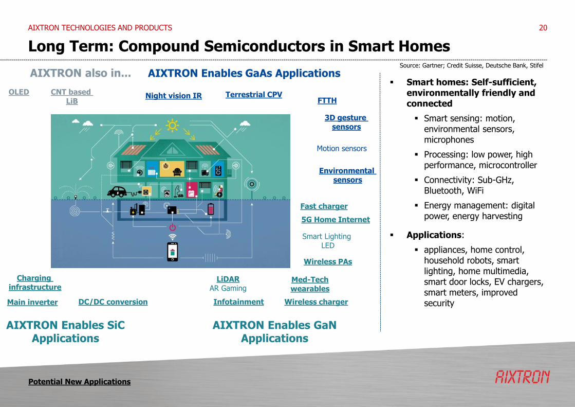
Long Term: Compound Semiconductors in Smart Homes
AIXTRON TECHNOLOGIES AND PRODUCTS 20
Motion sensors
Smart Lighting LED
5G Home Internet
Fast charger
OLED CNT based LiB
Charging infrastructure
DC/DC conversionMain inverter
Night vision IR
Environmental sensors
Terrestrial CPV
3D gesture sensors
FTTH
Wireless chargerInfotainment
Wireless PAs
Med-Tech wearables
LiDARAR Gaming
AIXTRON Enables GaAs Applications
AIXTRON Enables GaN Applications
AIXTRON Enables SiC Applications
AIXTRON also in... Smart homes: Self-sufficient,
environmentally friendly and connected
Smart sensing: motion, environmental sensors, microphones
Processing: low power, high performance, microcontroller
Connectivity: Sub-GHz, Bluetooth, WiFi
Energy management: digital power, energy harvesting
Applications:
appliances, home control, household robots, smart lighting, home multimedia, smart door locks, EV chargers, smart meters, improved security
Source: Gartner; Credit Suisse, Deutsche Bank, Stifel
Potential New Applications

Compound Semiconductors – Evolving Applications
AIXTRON TECHNOLOGIES AND PRODUCTS 21
AIXTRON Revenues CAGR 2013 -2016
2%
-9%
10%
25%
AIXTRONGroup
LEDEquipment
PowerEquipment
OptoelectronicEquipment
LED; 26%
Silicon; 21%Power
Electronics; 14%
Optoelectronics; 34%
Others; 5%
AIXTRON 2016 Revenuesby end application
(equipment only)

Compound Semiconductors – Wide-Band-Gap (WBG) Power Electronics
AIXTRON TECHNOLOGIES AND PRODUCTS 22
Consumer Electronics & IT Automotive Energy Industrial
Power Management
GaN
• Electronic appliances
• Computing
• Wireless charging
• Power supplies
• PFC
• Infotainment
• GPS
• Connected car
• Autonomous driving
• EMI/EMC
• Adaptive cruise control
GaN / SiC
• General automotive electronic
• HEV/EV
• Charging station
• Inverter / motor drives
• Converter
• Radar test applications
• Power Grid / Smart meter / appliances
• Solar / Wind inverters
• Solar / Wind power DC distribution
• storage
• UPS
• UPS
• Industrial machines
• Building
• Mining, oil, gas power generation
• Shipping/Rail
SiC
Power Switching
30V 600V 1.2 kV ≥2kV
Volume segment Niche segment
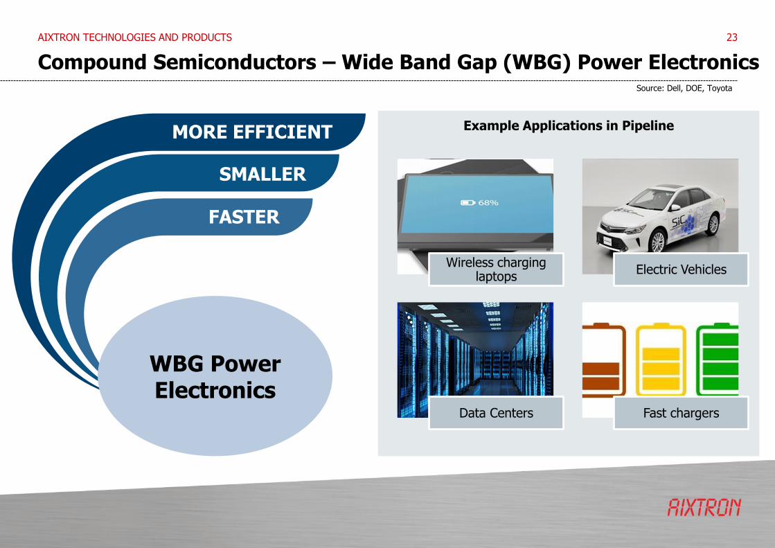
Example Applications in Pipeline
Compound Semiconductors – Wide Band Gap (WBG) Power Electronics
AIXTRON TECHNOLOGIES AND PRODUCTS 23
Source: Dell, DOE, Toyota
MORE EFFICIENT
SMALLER
FASTER
WBG Power Electronics
Wireless charging laptops
Electric Vehicles
Data Centers Fast chargers

Silicon Semiconductors – Leading Edge Technologies
24AIXTRON TECHNOLOGIES AND PRODUCTS
(2016: Indexed=1x)
Interconnects(Graphene/CNT)
Logic transistor(MOCVD- III-V)
Memory(ALD)
At the forefront to extend Moore’s Law
Source: Gartner 2016
2016 2020
~1.1x
>5x
To
tal
Fa
b C
ap
acit
ies ≤14nm Fab Capacities
“More than Moore”
Year
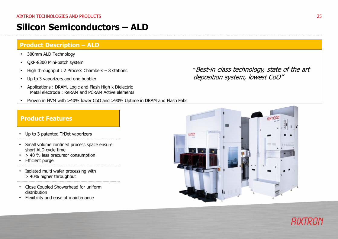
Silicon Semiconductors – ALD
25
Product Description – ALD
• Up to 3 patented TriJet vaporizers
• Small volume confined process space ensureshort ALD cycle time
• > 40 % less precursor consumption• Efficient purge
• Isolated multi wafer processing with> 40% higher throughput
• Close Coupled Showerhead for uniformdistribution
• Flexibility and ease of maintenance
• 300mm ALD Technology
• QXP-8300 Mini-batch system
• High throughput : 2 Process Chambers – 8 stations
• Up to 3 vaporizers and one bubbler
• Applications : DRAM, Logic and Flash High k Dielectric Metal electrode : ReRAM and PCRAM Active elements
• Proven in HVM with >40% lower CoO and >90% Uptime in DRAM and Flash Fabs
“Best-in class technology, state of the art deposition system, lowest CoO”
AIXTRON TECHNOLOGIES AND PRODUCTS
Product Features

Carbon Nanomaterials – PECVD
26
Product features
• Proprietary thermal and plasma enhanced chemical vapor deposition technology
• Excellent uniformity and reproducibility with fast turnaround cycle times
• BM platform: BM R&D (2-inch), BM Pro (4-inch and 6-inch), BM GB (4-inch glovebox), BM HT (high temperature, 1,700C), BM300T (300mm)
• Graphene and carbon nanotube films for electronics, energy storage, thermal management, sensors and flexible/transparent applications
Graphene and Carbon Nanotube Deposition Systems
• Fast response heater and turnaround
• Thermal CVD
• Substrate and top heating
• Closed loop infrared wafer temperature control
• Plasma enhanced CVD with frequency control
• Flexible processing for different applications
• Low cost of ownership
• Easy maintenance and cleaning
• User management features and growth library
Graphene (2D) and Carbon nanotube (1D)
Unique combination of high electrical/ thermal conductivity, mobility, flexibility and transparency
Serving R&D market today
AIXTRON BM Pro
Production ready for tomorrow
AIXTRON BM Pro 300
MaterialProperties
AIXTRONTechnology
EnablingApplications
AIXTRON TECHNOLOGIES AND PRODUCTS
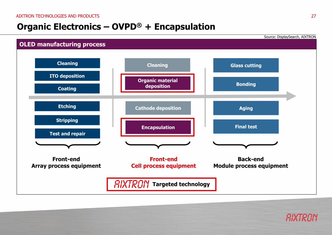
Organic Electronics – OVPD® + Encapsulation
AIXTRON TECHNOLOGIES AND PRODUCTS 27
Source: DisplaySearch, AIXTRON
Front-endArray process equipment
Front-endCell process equipment
Coating
Etching
Stripping
Test and repair
ITO deposition
Cleaning
Organic material deposition
Encapsulation
Cathode deposition
Cleaning Glass cutting
Bonding
Aging
Final test
Back-endModule process equipment
Targeted technology
OLED manufacturing process

Proprietary carrier-gas enhanced gas phase deposition approach for organic thin films
Based on AIXTRON‘s core competence of carrier gas enhanced vapor phase deposition
Free scalability: suitable for all relevant substrate generations
Manufacturing technology applicable for OLED displays, OLED lighting, organic semiconductors, and organic photovoltaic
Proprietary STExS™ evaporation source technology: low thermal stress, high rates, continuous operation
High deposition rates for high throughput Reduced thermal stress for organic materials
High material utilization efficiency Flexible process control
Simplified scaling due to Close Coupled Showerhead and Decoupled source technology
Flexible integration solutions batch and inline Reduced number of deposition chamber and
footprint Scalable: Available for substrate sizes
up to Gen8.5 (=2.3 x 2.5 m²)
Organic Electronics – OVPD®
Product Description – OVPD
“Disruptive deposition technology for cost efficient OLED manufacturing”
AIXTRON TECHNOLOGIES AND PRODUCTS
Product Features
28
OVPD demonstrator OLAD (Organic Large Area Demonstrator)(optimized for Generation 8.5 substrate sizes)

Proprietary PECVD technology based on linear plasma sources
Based on AIXTRON‘s core competence of carrier gas enhanced vapor phase deposition
Free scalability: suitable for all relevant substrate generations
Manufacturing technology applicable for barrier applications, i.e. thin film encapsulation:highly flexible, low film stress, high transparent, high water and oxygen permeation barrier,
High deposition rates for high throughput Flexible process control
Simplified scaling due to Linear PECVD source technology Multiple source configurations
Scalable: Available for substrate sizes up to Gen3.5, future: up to Gen8.5
Highly flexible SiNx-based barrier films at high rates
Low temperature process (<80°) with low film stress
Organic Electronics – OPTACAP™ PECVD
Product Description – OptaCap™ PECVD
“Disruptive deposition technology for cost efficient deposition of flexible barrier films”
AIXTRON TECHNOLOGIES AND PRODUCTS
Product Features
OPTACAP-200 200x200 mm² Substrates
29
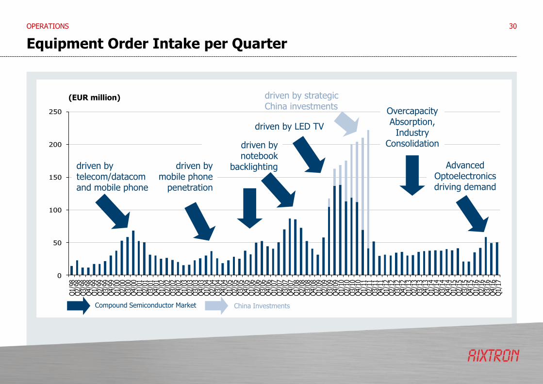
Equipment Order Intake per Quarter
OPERATIONS 30
0
50
100
150
200
250
Q1/
98Q
2/98
Q3/
98Q
4/98
Q1/
99Q
2/99
Q3/
99Q
4/99
Q1/
00Q
2/00
Q3/
00Q
4/00
Q1/
01Q
2/01
Q3/
01Q
4/01
Q1/
02Q
2/02
Q3/
02Q
4/02
Q1/
03Q
2/03
Q3/
03Q
4/03
Q1/
04Q
2/04
Q3/
04Q
4/04
Q1/
05Q
2/05
Q3/
05Q
4/05
Q1/
06Q
2/06
Q3/
06Q
4/06
Q1/
07Q
2/07
Q3/
07Q
4/07
Q1/
08Q
2/08
Q3/
08Q
4/08
Q1/
09Q
2/09
Q3/
09Q
4/09
Q1/
10Q
2/10
Q3/
10Q
4/10
Q1/
11Q
2/11
Q3/
11Q
4/11
Q1/
12Q
2/12
Q3/
12Q
4/12
Q1/
13Q
2/13
Q3/
13Q
4/13
Q1/
14Q
2/14
Q3/
14Q
4/14
Q1/
15Q
2/15
Q3/
15Q
4/15
Q1/
16Q
2/16
Q3/
16Q
4/16
Q1/
17
Compound Semiconductor Market China Investments
driven by notebook
backlighting
driven by LED TV
driven by strategic China investments
(EUR million)
driven by mobile phone
penetration
driven by telecom/datacomand mobile phone
Overcapacity Absorption,
Industry Consolidation
Advanced Optoelectronics driving demand

Annual Equipment Revenues by Application (excl. spares)
OPERATIONS 31
0
100
200
300
400
500
600
700
800
1999 2000 2001 2002 2003 2004 2005 2006 2007 2008 2009 2010 2011 2012 2013 2014 2015 2016
LED Silicon Power Electronics Optoelectronics* Others
(EUR million)
* Optoelectronics includes applications in Consumer Optoelectronics, Telecom/Datacom, Solar, etc.

Organic
Silicon
Competitive Landscape
INDUSTRY 32
MOCVD
GaAs/InP: Advanced Optoelectronics, ROY LEDs
GaN LED
GaN Power
SiC Power
(TOPEC)
Consolidated Income Statement*
FINANCIALS 33
(€ million) 2014 2015 2016
Revenues 193.8 197.8 196.5
Cost of sales 154.1** 147.9 140.2
Gross profit 39.7** 49.8 56.3
Gross Margin 20% 25% 29%
Selling expenses 14.1** 11.5 13.8
General & admin expenses 19.3 16.3 17.1
R&D 66.7 55.4 53.9
Net other operating income & expenses -2.2 -6.7 -7.2
EBITDA -41.3 -16.4 -7.9
EBIT -58.3 -26.7 -21.4
EBIT Margin -30% -14% -11%
Result before tax -57.1 -26.0 -21.0
Pre-Tax Margin -29% -13% -11%
Net result -62.5 -29.2 -24.0
Net Return on Sales -32% -15% -12%
*) rounded figures; may not add up**) 2014 figures adjusted to be comparable
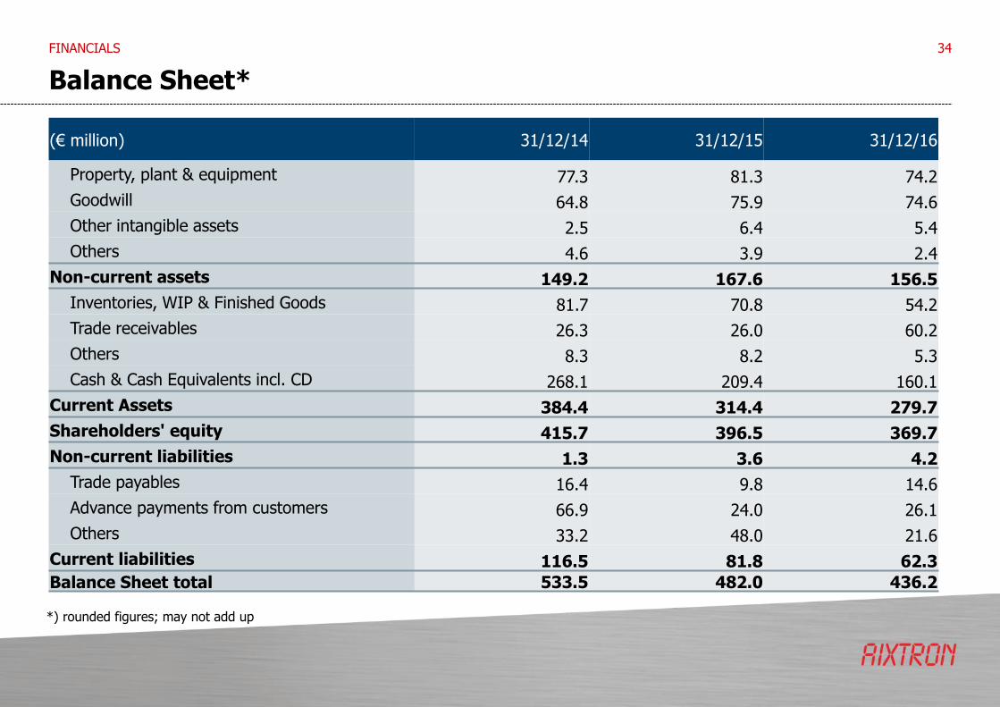
Balance Sheet*
34
*) rounded figures; may not add up
(€ million) 31/12/14 31/12/15 31/12/16
Property, plant & equipment 77.3 81.3 74.2
Goodwill 64.8 75.9 74.6
Other intangible assets 2.5 6.4 5.4
Others 4.6 3.9 2.4
Non-current assets 149.2 167.6 156.5
Inventories, WIP & Finished Goods 81.7 70.8 54.2
Trade receivables 26.3 26.0 60.2
Others 8.3 8.2 5.3
Cash & Cash Equivalents incl. CD 268.1 209.4 160.1
Current Assets 384.4 314.4 279.7
Shareholders' equity 415.7 396.5 369.7
Non-current liabilities 1.3 3.6 4.2
Trade payables 16.4 9.8 14.6
Advance payments from customers 66.9 24.0 26.1
Others 33.2 48.0 21.6
Current liabilities 116.5 81.8 62.3
Balance Sheet total 533.5 482.0 436.2
FINANCIALS

Consolidated Statement of Cash Flows*
FINANCIALS 35
(€ million) 2014 2015 2016
Cash Flow from operating activities -33.8 -45.7 -37.7
Cash Flow from investing activities -23.2 41.2 43.4
Cash Flow from financing activities 0.2 -0.1 0.3
Exchange rate changes 5.9 4.3 -2.3
Net change in Cash & Cash Equivalents -50.9 -0.3 3.7
Cash & Cash Equivalents (beginning of period) 167.5 116.6 116.3
Cash & Cash Equivalents (end of period) 116.6 116.3 120.0
Change in Cash deposits 9.9 -60.5 -52.8
Free Cash Flow** -47.0 -57.3 -42.9
Capex 13.4 13.3 5.3
*) rounded figures; may not add up**) Operating CF + Investing CF + Changes in Cash Deposits, adjusted for acquisition effects
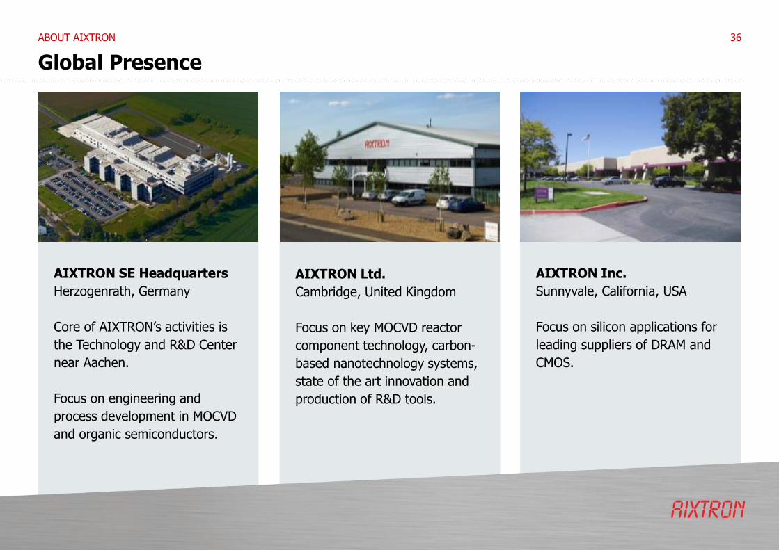
Global Presence
AIXTRON SE Headquarters
Herzogenrath, Germany
Core of AIXTRON’s activities is
the Technology and R&D Center
near Aachen.
Focus on engineering and
process development in MOCVD
and organic semiconductors.
AIXTRON Inc.
Sunnyvale, California, USA
Focus on silicon applications for
leading suppliers of DRAM and
CMOS.
AIXTRON Ltd.
Cambridge, United Kingdom
Focus on key MOCVD reactor
component technology, carbon-
based nanotechnology systems,
state of the art innovation and
production of R&D tools.
36ABOUT AIXTRON

Financial Calendar & Contact Data
• May 9, 2017 Annual General Meeting, Aachen
• July 25, 2017 H1/2017 Results, Conference Call
• October 26, 2017 9M/2017 Results, Conference Call
• February 2018 FY/2017 Results, Conference Call
For further information please contact:
Investor Relations & Corporate CommunicationsAIXTRON SE Dornkaulstr. 2 52134 Herzogenrath, Germany
IR Team EuropePhone: +49 (2407) 9030-444 E-Mail: [email protected]
IR Team USA – Andrea SuPhone: +1 (408) 747-7140 ext. 1292 E-Mail: [email protected]
37
AIXTRON SEDornkaulstr. 252134 HerzogenrathGermanyPhone +49 (2407) 9030-0Fax +49 (2407) 9030-40E-Mail [email protected]
Thank you very much for your attention.