aim: - apparatus: - s.no theory:- -...
TRANSCRIPT

LENDI Power Electronics Laboratory
Dept. of EEE 1
CHARACTERISTICS OF SCR
Aim: - 1. To get the characteristics of the SCR for different gate currents.
2. To obtain the Holding current and Latching current of the SCR Apparatus: -
s.no Item Type & Range Quantity
1. SCR TYN 616s;Vrrm = 600V, Itrms - 16amps,
1No
2. Volt meter Moving Coil ( 0-50 volts) 1No
3. Ammeters Moving Coil ( 0-500 mA ) & ( 0-25mA)
1No 1 No
4. Patch Cards Adequate
Theory:-
Circuit diagram:-
IA
VAK
IG
R2
V2
0-500mA R1
V10-50V10K
4K
Exp. - 1

LENDI Power Electronics Laboratory
Dept. of EEE 2
Procedure: -
a) SCR characteristics
i)V-I Characteristics :
Make the connections as given in the circuit diagram. Now switch ON the mains supply to the unit and initially keep V1 & V2 at minimum. Set load potentiometer R1 in the minimum position.. Adjust Ig – Ig1 say 10 mA by varying V2 or gate current potentiometer R2. Slowly vary V1 and note down VAK and IA readings for every 5 volts and enter the readings in the tabular column. Further vary V1 till SCR conducts, this can be noticed by sudden drop of VAK and rise of IA readings. Note down this reading and tabulate. Vary V1 further and note down IA and VAK readings. Draw the graph of VAK v/s IA.Repeat the same for Ig = Ig2 / Ig3 mA and draw the graph.
ii) Tabular Column:
Ig2 (mA)
VAK (Volts) IA (mA)
iii) To find latching current: Apply about 20 V between anode and cathode by varying V1. Keep the load potentiometer R1at minimum position. The device must be in the OFF state with gate open. Gradually increase Gate voltage – V2 till the device turns )N. This is the minimum gate current (Igmin) required to turn ON the device. Adjust the gate voltage to a slightly higher value. Set the load potentiometer at the maximum resistance position. The gate voltage to OFF state, otherwise decrease V1 till the device comes to OFF state. The gate voltage should be kept constant in this experiment. By varying R1, gradually increase anode current IA in steps. Open and close the Gate voltage V2 switch after each step . If the anode current is greater than the latching current of the device goes into blocking mode as soon as the gate switch is opened. Note the latching current. Obtain more accurate value of the latching current by taking small steps of IA near the latching current value.
Increase the anode current from the latching current level by load pot R1 or V1. Open the gate switch permanently. The thyristor must be fully ON. Now start reducing the anode current gradually by adjusting R1. If the thyristor does not turns OFF even after the R1 at maximum position, then reduce V1. Observe when the device goes to blocking mode. The anode current through the device at this instant is the holding current of the device. Repeat the steps again to accurately get the IH. Normally IH < IL.
b)MOSFET
i)Trans Conductance Chracteristics:
Make the connections as shown in the circuit digram including meters. Initially keep V1 and V2 minimum. Set V1= VDS1= say 10v . Slowly vary V2 (VGS) and note down ID and VGS Readings for every 1 Volt and enter in the tabular column. The minimum gate voltage VGS that is required for conduction to start the MOSFET is called Threshold Voltage VGS(tH). The Drain current depends on magnitude of the Gate Voltage VGS which may vary from 2 to 5 volts.Repeat the same for different VDS and draw the graph of VGS V/s ID.
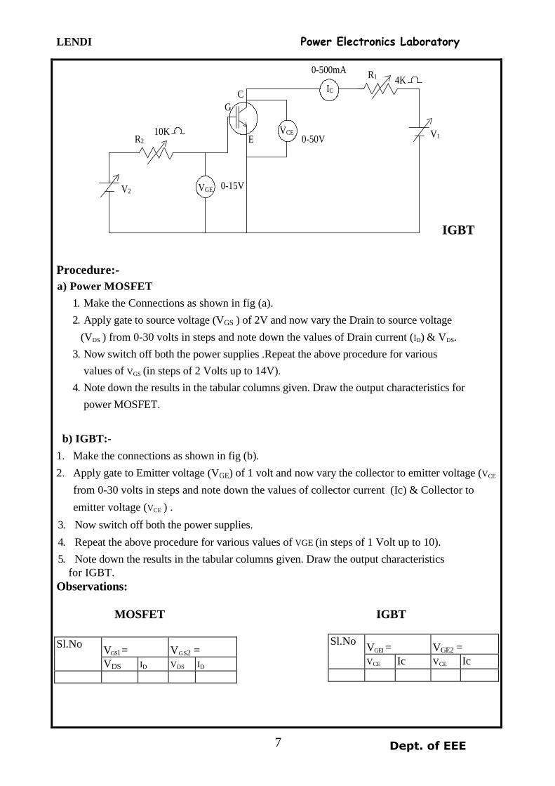
C)IGBT
Ig1 (mA)
VAK (Volts) IA (mA)

LENDI Power Electronics Laboratory
Dept. of EEE 3
i) Transfer Characteristics:
Make the connections as shown in the circuit diagram with meters. Initially keep V1 and V2 minimum. Set V1 = VCE1 = say 10 V. Slowly vary V2 (VGE) and note down Ic and VGE readings for every 1.0 Volt and enter in the tabular column. The minimum gate voltage VGE which is required for conduction to start the IGBT is called threshold Voltage VGE(Th). If VGE is greater than VGE(Th) only very small leakage current flows from Collector to Emitter. If VGE is greater than VGE(Th), The collector current depends on magnitude of the Gate Voltage. VGE Varies from 4 to 8 Volts. Repeat the same for Vc and draw the graph of VGE V/S IC.
ii) Tabular Column:
VCE1(Volts) VCE2 (Volts)
VGE (volts) IC (mA) VGE(Volts) IC (mA)
iii) Collector Characteristics:
Initially set V2 to VGE1 = 5 Volts. Slowly vary V1 and note down IC and VGE. For a particular value of VGE1 there is a pinch off voltage (Vp) between Collector and Emitter.
If VGE is lower than Vp the device works in the constant resistance region and IC is directlyl proportional to VGE. If VGE is more than Vp constant IC flows from the device and this operating region is called constant current region.Repeat the above for different values of VGE and note down VCE V/S IC.Draw the graph of VCE V/S IC for different values of VGE.
iv) Drain Characteristics:
Initially set V2 to VGS1 = 3.5 Volts. Slowly vary V1 and note down ID and VDS. For a particular value of VGS1 there is a pinch off voltage (Vp) between drain and source. If VDS is lower than Vp’ the device works in the constant resistance region and ID flows from the device and this operating region is called constant current region.
Repeat the above for different values of VGS and note down VDS Vs ID.Draw the graph of VDS Vs ID for different values of VGS.
v) Tabular Column:
VDS1(Volts) VDS2 (Volts)
VGS (volts) ID (mA) VGS(Volts) ID (mA)
VGS1(Volts) VGS2 (Volts)

LENDI Power Electronics Laboratory
Dept. of EEE 4
VDS (volts) ID (mA) VDS(Volts) ID (mA)
b) To get Latching current:-
1. Connections are made as per circuit diagram.
2. Adjust the DC1 potentiometer to some voltage (say 2v) and apply gate signal so that the flowing of anode current in the circuit and the voltage across anode to cathode falls indicates SCR fires and it.
3. Now open the gate terminal and observe whether the SCR is in ON state or OFF state.
4. If the SCR is in OFF state, the anode current is not sufficient to keep the device in conduction.
5. Increase the anode current gradually (by varying DC1 Pot) so that the device continues to conduct even after the gate drive is removed.
Read the minimum anode current as Latching current.
c) To get Holding current
1. Connections are made as per circuit diagram.
2. Adjust the DC1 potentiometer to some voltage (say 2v) and apply gate signal so that SCR fires and it is indicated by the flowing of anode current in the circuit and the
- voltage across anode to cathode falls.
3. Reduce the anode current gradually (by varying DC1 pot & DC2 pot till the device gets turned OFF).
4. Read the minimum anode current below which SCR turns OFF. It is holding current. Observations:-
S.No Vak Volts Iak mA
S.No Vak Volts IakmA

LENDI Power Electronics Laboratory
Dept. of EEE 5
Model graph:-
Precautions:-
1) Ensure that connections are given properly before switching on power supply. 2) The readings must be noticed carefully without parallax error. 3) The student must wear leather chappels or shoes in the laboratory. 4) One must be aware of first-Aid techniques for elelctric-shock
Review Questions :-
1. How many methods of gate control are available for triggering SCRs &what are they?
2. What are the different operating regions of SCR? And explain them?
3. Give some industrial applications of the SCR ?
Results:- The characteristics of SCR for different values of gate current was obtained . Holding current IH = , Latching current Ic= ,
CHARACTERISTICS OF POWER MOSFET & IGBT

LENDI Power Electronics Laboratory
Dept. of EEE 6
Aim:- To study the static characteristics of MOSFET & IGBT. Apparatus:-
Theory:-
Circuit Diagram :
ID
VDSR2
V2
0-500mA R1
V10-50V10K
4KD
S
VGS
MOS FET
S.No Item Type / Range Quantity
1. MOSFET
IRF 840, VDS : 400V, Max I D : 10Amps,
1No 2. IGBT IMBH60D, VCE : 500Volts Max Ic 8A 1No
3. Volt meter DC, 0-50volts 1No
4. Ammeter DC, 0- 500mA 1No
5. Voltmeter DC, 0-15volts 1No
6. DC Regulated Power supply 0-30 volts/5A 1No
7. Connecting probes Adequate
LENDI Power Electronics Laboratory
Dept. of EEE 7
IC
VCER2
V2
0-500mA R1
V10-50V10K
4KC
E
VGE
G
0-15V
IGBT
Procedure:- a) Power MOSFET
1. Make the Connections as shown in fig (a).
2. Apply gate to source voltage (VGS ) of 2V and now vary the Drain to source voltage
(VDS ) from 0-30 volts in steps and note down the values of Drain current (ID) & V DS.
3. Now switch off both the power supplies .Repeat the above procedure for various
values of VGS (in steps of 2 Volts up to 14V).
4. Note down the results in the tabular columns given. Draw the output characteristics for
power MOSFET.
b) IGBT:-
1. Make the connections as shown in fig (b).
2. Apply gate to Emitter voltage (VGE) of 1 volt and now vary the collector to emitter voltage (VCE
from 0-30 volts in steps and note down the values of collector current (Ic) & Collector to
emitter voltage (VCE ) .
3. Now switch off both the power supplies.
4. Repeat the above procedure for various values of VGE (in steps of 1 Volt up to 10).
5. Note down the results in the tabular columns given. Draw the output characteristics for IGBT. Observations: MOSFET IGBT
Sl.No VGS1 = VGS2 = VDS ID VDS ID
Sl.No VGEI = VGE2 = VCE Ic VCE Ic

LENDI Power Electronics Laboratory
Dept. of EEE 8
Model graphs :-
Precautions:- 1) Ensure that connections are given properly before switching on the power supply.
2) The readings must be noticed carefully without parallax error.
3) One must be aware of first-Aid techniques for electric-shock
Review Questions :-
1. What is MOSFET ? What are the types of MOSFETs?
2. Discuss pinch off voltage , Treshold voltage ,turn on., turn off with reference to MOSFET?
3. What are the advantages & disadvantage of a MOSFET?
4. What is IGBT ?
5. IGBT imparts the characteristics of two devices, what are they?
6. Among IGBT, MOSFET, BJT and Thyristor which belongs to current controlled device category. And rest of them belongs to which category?

LENDI Power Electronics Laboratory
Dept. of EEE 9
GATE FIRING CIRCUITS FOR SCR
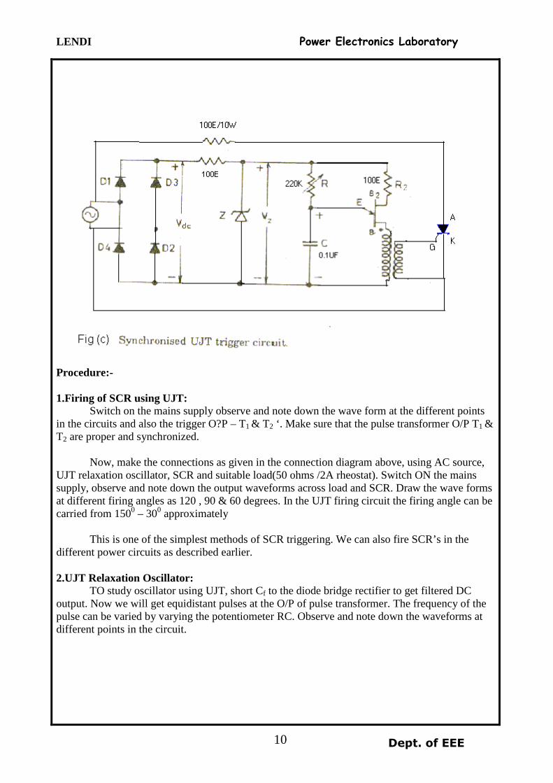
Aim:- To study various firing schemes for triggering of SCRs when they are connected in different converter topologies employing line commutation. They are (a) Resistance firing circuit (b) RC trigger circuit (C) U.J.T trigger circuit.
Apparatus:- Resistance firing circuit kit, RC Firing circuit kit , UJT firing circuit kit.
-
Theory:- Circuit diagram:-
S. No Item Type & Range Quantity 1. SCR f i r ing un i t TYN612 600V/ 12A, 1 No 2. Diode IN4002 1NO 3. UJT 2N2646 1NO
4. Isolation transformer 230/115-0-115, 1:1 ratio 1 NO 5. Resistive load 100E/10W 1 NO
6 Zener diode 15v/1w 1 NO
7. Patch Cards Adequate
Exp. - 2
LENDI Power Electronics Laboratory
Dept. of EEE 10
Procedure:- 1.Firing of SCR using UJT: Switch on the mains supply observe and note down the wave form at the different points in the circuits and also the trigger O?P – T1 & T2 ‘. Make sure that the pulse transformer O/P T1 & T2 are proper and synchronized. Now, make the connections as given in the connection diagram above, using AC source, UJT relaxation oscillator, SCR and suitable load(50 ohms /2A rheostat). Switch ON the mains supply, observe and note down the output waveforms across load and SCR. Draw the wave forms at different firing angles as 120 , 90 & 60 degrees. In the UJT firing circuit the firing angle can be carried from 1500 – 300 approximately This is one of the simplest methods of SCR triggering. We can also fire SCR’s in the different power circuits as described earlier. 2.UJT Relaxation Oscillator: TO study oscillator using UJT, short Cf to the diode bridge rectifier to get filtered DC output. Now we will get equidistant pulses at the O/P of pulse transformer. The frequency of the pulse can be varied by varying the potentiometer RC. Observe and note down the waveforms at different points in the circuit.
LENDI Power Electronics Laboratory
Dept. of EEE 11
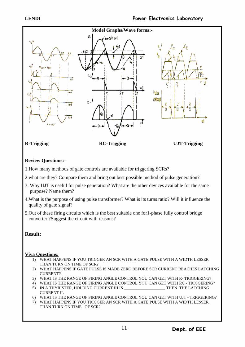
Model Graphs/Wave forms:-
R-Trigging RC-Trigging UJT-Trigging
Review Questions:-
1.How many methods of gate controls are available for triggering SCRs?
2.what are they? Compare them and bring out best possible method of pulse generation?
3. Why UJT is useful for pulse generation? What are the other devices available for the same purpose? Name them?
4.What is the purpose of using pulse transformer? What is its turns ratio? Will it influence the quality of gate signal?
5.Out of these firing circuits which is the best suitable one for1-phase fully control bridge converter ?Suggest the circuit with reasons?
Result:
Viva Questions:
1) WHAT HAPPENS IF YOU TRIGGER AN SCR WITH A GATE PULSE WITH A WIDTH LESSER THAN TURN ON TIME OF SCR?
2) WHAT HAPPENS IF GATE PULSE IS MADE ZERO BEFORE SCR CURRENT REACHES LATCHING CURRENT?
3) WHAT IS THE RANGE OF FIRING ANGLE CONTROL YOU CAN GET WITH R- TRIGGERING? 4) WHAT IS THE RANGE OF FIRING ANGLE CONTROL YOU CAN GET WITH RC - TRIGGERING? 5) IN A THYRISTER, HOLDING CURRENT IH IS ____________________ THEN THE LATCHING
CURRENT IL 6) WHAT IS THE RANGE OF FIRING ANGLE CONTROL YOU CAN GET WITH UJT - TRIGGERING? 7) WHAT HAPPENS IF YOU TRIGGER AN SCR WITH A GATE PULSE WITH A WIDTH LESSER
THAN TURN ON TIME OF SCR?

LENDI Power Electronics Laboratory
Dept. of EEE 12
1-Ф AC VOLTAGE CONTROLLER WITH R AND RL LOADS
Aim:- To study the operation of an AC voltage controller.
Apparatus:-
Theory:-
Circuit Diagram:-
230V,50Hz AC
230V,50Hz AC
24V
24V
0VT2
T1
LOAD
R&RL
24V
24V
0V
LOAD
R&RL
STEP DOWN TRANSFORMER
S. No Item Type & Range Quantity 1. l - � AC voltage
controller power circuit circuitcircuit converter
- 1 No
2. 1 -�avc firing unit - 1NO 3. CRO - 1NO
4. Connecting wires - Required No 5. Rheostat 50ohm/5A 1 NO
6. Inductor with tappings
50mH / 2 A,
1 NO 1 NO
Exp. - 3
LENDI Power Electronics Laboratory
Dept. of EEE 13
Procedure:-
1. Make the connections as per circuit diagram .Switch on the mains supply to the firing circuit and observe the trigger out puts by varying firing angle potentiometer and by operating ON/OFF and SCR/Triac selector switch. Make sure that the trigger pulses are coming properly before connecting to the power circuit .
2. Connect the trigger pulses from the firing circuit to the corresponding SCRs in the power ckt.
3. Connect AC supply to the power circuit through step down transformer.
4. Connect 50 ohms / 5w resistive load in Fig (a).
5. Switch ON the power supply and trigger outputs and observe the output voltage wave
forms across load and SCR.
6. For a given input voltage note down the out put voltage and current for different values of firing angle.
7. Repeat the steps 5 & 6 by connecting the 100mH inductive load in series with
50 ohms / 5w rheostat.
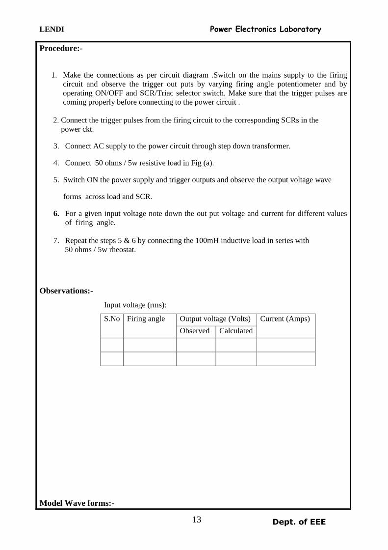
Observations:-
Input voltage (rms):
S.No Firing angle Output voltage (Volts) Current (Amps) Observed Calculated
Model Wave forms:-

LENDI Power Electronics Laboratory
Dept. of EEE 14
a) Resistive load
(b) R-L Load

LENDI Power Electronics Laboratory
Dept. of EEE 15
Precautions:-
1) Ensure that connections are given properly before switching on the power supply.
2) The readings must be noticed care fully without parallax error.
3) One must be aware of first-Aid techniques for electric shock.
4) If there is no output even after all the proper connections, switch OFF the supply and just Interchange the connections at step down transformer terminals. This is to make the power circuit and firing circuit to synchronize.
Review Questions:- 1. What is phase angle control? What are the advantages and disadvantages of phase
angle control ?
2. What is the effect of load inductance on the performance of AC Voltage controller?
3. What is the relationship between firing angle and RMS out put voltage?
4. What are the applications of A.C. voltage controller?
5. What is the semiconductor device that can be used as an AC voltage controller?
6. What are its limitations? How we can turn off SCR in A.C. voltage controller? Results:
l-� FULLY CONTROLLED BRIDGE CONVERTER WITH R & RL LOAD S
Aim:- To study the voltage waveforms across R and RL loads connected to single phase fully controlled converter.
Apparatus:-
Exp. - 4

LENDI Power Electronics Laboratory
Dept. of EEE 16
Theory:-
Circuit diagram:-
230V,50HzAC
T1T3
T4 T2
Dm
R
L
V0
Procedure:-
1. Switch ON the firing circuit, and check the firing pulses. 2. Connect the power circuit, Firing circuit, Load as per the circuit diagram. 3. Give 1-� ,230V 50Hz supp ly to the power c i r cu i t b y c los ing PST
swi tch
S. No Item Type & Range Quantity 1. l - � full converter
power circuit 230V/ 5A, 1 No
2. 1 -� converter firing unit 5V, 200mA 1NO 3. 1-� Isolation transformer 230/230V 1NO
4. Resistor 50ohm/5A 1 NO 5. Inductor 150mH,2A 1 NO 6
Ammeter
0-5A,M.C 1 NO
7. Voltmeter 0-300V,M.C 1 NO 8. Attenuation Probes 10:1 1 NO
LENDI Power Electronics Laboratory
Dept. of EEE 17
4. Switch ON the firing pulses to SCRs by keeping ON/OFF soft switch in ON position.
5. Observe the load voltage wave and current wave (using shunt element of 1 ohm) 6. Record load voltage and current by varying firing angle of SCR from voltmeter and
ammeter. 7. After completion of experiment switch OFF power circuit first then firing circuit. 8. Plot the graph between firing angle and output voltage.
Note : If the output shows zero even after making the connections properly, switch off the
input supply and interchange the input supply terminals. This is to make the input supply
to the firing unit and the power circuit in the same phase. If they are just opposite in
phase, none of the SCRs will trigger and output will be zero.
Observations:-
S.No Input voltage, Vin Firing Angle Load current, IL Load voltage VL Practical Theoretical
Sample Calculations:-
Vo = π
mV2cos a,
Io = Vo / R
Vignan’s IIT, Vizag Power Electronics Laboratory
Dept. of EEE 18
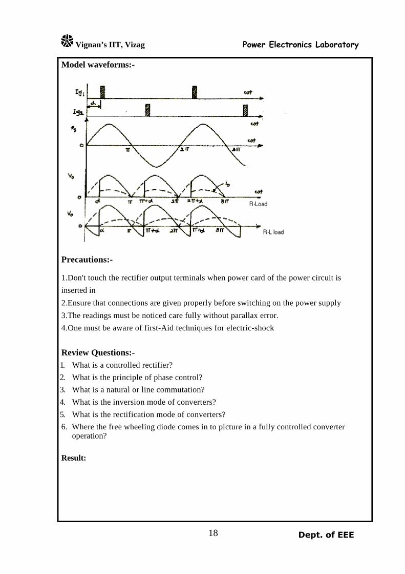
Model waveforms:-
Precautions:-
1.Don't touch the rectifier output terminals when power card of the power circuit is
inserted in
2.Ensure that connections are given properly before switching on the power supply
3.The readings must be noticed care fully without parallax error.
4.One must be aware of first-Aid techniques for electric-shock
Review Questions:- 1. What is a controlled rectifier?
2. What is the principle of phase control?
3. What is a natural or line commutation?
4. What is the inversion mode of converters?
5. What is the rectification mode of converters?
6. Where the free wheeling diode comes in to picture in a fully controlled converter operation?
Result:
Vignan’s IIT, Vizag Power Electronics Laboratory
Dept. of EEE 19
FORCED COMMUTATION CIRCUITS
Aim:- To study the four types of commutation circuits (Class A, Class B, Class C and Class D)
Apparatus:- Name Plate details:- SCR V =1200V, I = 40 amps, Diode V:1200V, I = 40amps, Capacitors: C1– 2.2 uF, C2 – 10uf , Inductor L – 250 uH, 500uH,1mH . Theory:-
SI.No Item Type / Range Quantity 1. Force commutation kit I No 2. CRO with 10:1 probe 20MHz 1 No 3. Connecting wires Adequate 4. Rheostats 50ohm/2A 2 Nos
Exp. - 5
Vignan’s IIT, Vizag Power Electronics Laboratory
Dept. of EEE 20
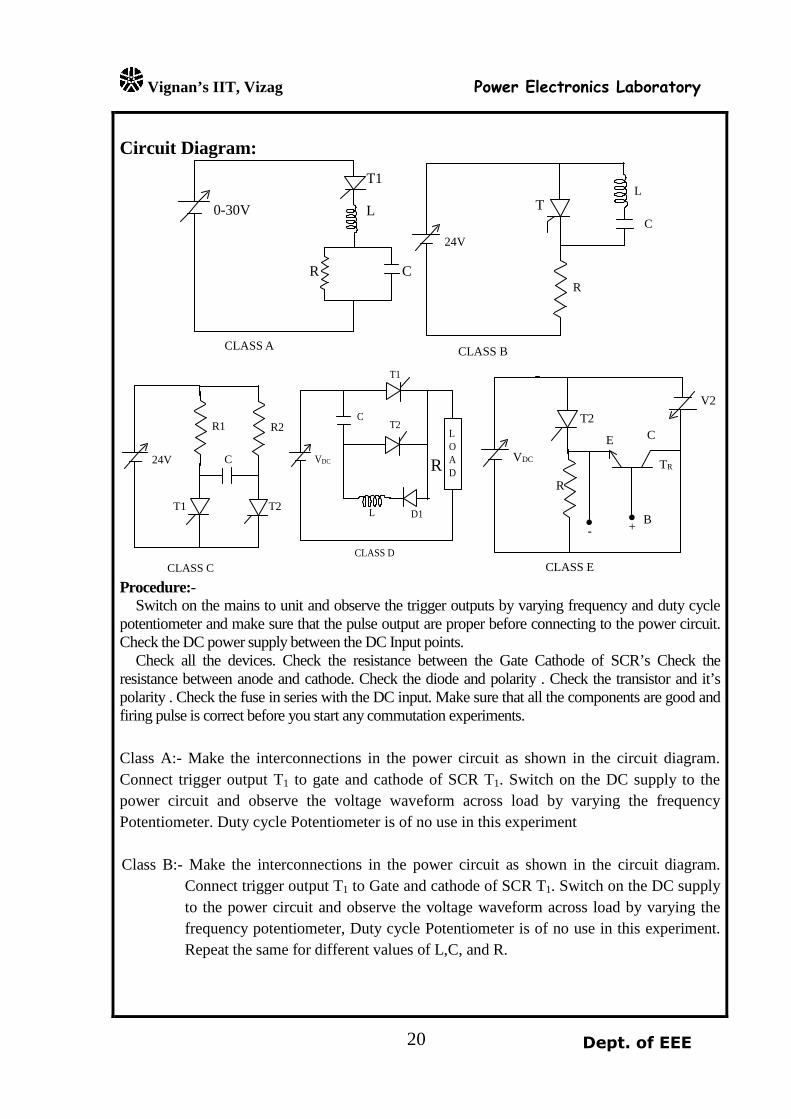
Circuit Diagram:
L
C
R
24V
24V
R1 R2
T1 T2
C VDC
T1
CT2
D1L
LOADR
VDC
T2
V2
- +
E C
TR
B
R
T0-30V L
R C
T1
CLASS A CLASS B
CLASS CCLASS D
CLASS E Procedure:- Switch on the mains to unit and observe the trigger outputs by varying frequency and duty cycle potentiometer and make sure that the pulse output are proper before connecting to the power circuit. Check the DC power supply between the DC Input points. Check all the devices. Check the resistance between the Gate Cathode of SCR’s Check the resistance between anode and cathode. Check the diode and polarity . Check the transistor and it’s polarity . Check the fuse in series with the DC input. Make sure that all the components are good and firing pulse is correct before you start any commutation experiments. Class A:- Make the interconnections in the power circuit as shown in the circuit diagram. Connect trigger output T1 to gate and cathode of SCR T1. Switch on the DC supply to the power circuit and observe the voltage waveform across load by varying the frequency Potentiometer. Duty cycle Potentiometer is of no use in this experiment Class B:- Make the interconnections in the power circuit as shown in the circuit diagram.
Connect trigger output T1 to Gate and cathode of SCR T1. Switch on the DC supply to the power circuit and observe the voltage waveform across load by varying the frequency potentiometer, Duty cycle Potentiometer is of no use in this experiment. Repeat the same for different values of L,C, and R.

Vignan’s IIT, Vizag Power Electronics Laboratory
Dept. of EEE 21
Class C:- Make the inter connections as shown in the circuit diagram. Connect T1 and T2 from firing circuit to gate and cathode of Thyristor T1 and T2 . Observe the wave forms across R1, R2 C by varying frequency and also duty cycle potentiometers. Repeat the same for different values of C and R . In this circuit L is of no use. Class D:- Make the connections as given in the circuit diagram. Connect T1 and T2 gate pulse from the firing circuit to the corresponding SCR’s in the power circuit. Initially keep the trigger ON/OFF at OFF position to initially change the capacitor, this can be observed by connecting CRO across the capacitor. Now Switch ON the trigger O/P switch and observe the voltage wave forms at different frequencies of chopping and also different duty cycles. Repeat the experiments for different values of load resistance, communication inductance and capacitance. Class E: Make the connections as shown in the circuit diagram. Connect the trigger output T1 from the firing circuit to the SCr. Connect T2 to the transistor base and emitter points. Switch on the DC supply and external Dc supply. Switch on the trigger output and observe and note down waveforms across the load. Repeat the same by varying frequency and duty cycle. Model waveforms:-

Vignan’s IIT, Vizag Power Electronics Laboratory
Dept. of EEE 22
Precautions :-
1) Ensure that connections are given properly before switching on the power supply. 2) The readings must be noticed care fully without parallax error. 3) One must be aware of first-Aid techniques for electric-shock
Review questions:-
1 .What is the difference between self and natural commutation? 2. What is principle of self commutation? 3. what are the differences between Voltage and current commutation?
4. what is the purpose of commutation circuit? 5. Why should be the reverse bias time greater than the turn-off time of an SCR? 6. How the voltage of commutation capacitor is reversed in a commutation circuit? Results:-

Vignan’s IIT, Vizag Power Electronics Laboratory
Dept. of EEE 23
JONES CHOPPER Aim:- To observe the load voltage wave forms of JONES CHOPPER
Apparatus:-
Sl. No Item Type / Range Quantity
1. DC Chopper power circuit 30V/2A 1N0
2. DC Chopper firing circuit 5V/200mA 1No
3. Regulated Power supply, 30 volts@ 2Amps 1No
4. C.R.O. with 10:1Probe, - 1No
5. Connecting wires Few
6. Rheostat 50 Ohms, 2Amp 1No
7. Inductor 150mH/2A 1No
Theory:- Circuit diagram:-
LOAD
DM
D1
T2
T1
C10uFVDC
L1 L2LM
500MH
500MH
Exp. - 6

Vignan’s IIT, Vizag Power Electronics Laboratory
Dept. of EEE 24
Procedure:-
1. Switch on the Chopper firing circuit and check the trigger output signal by varying duty
cycle and frequency pots keeping control switch in to INT position.
2. Connect the power supply, chopper power circuit, chopper firing circuit and load as per
circuit diagram.
3. Switch ON the 30V DC supply to the chopper power circuit.
4. Switch ON the 1 - Ф, 230 V 50 Hz input supply of chopper firing circuit.
5. Apply main SCR trigger pulses by pressing ON/OFF switch to ON position.
6. Observe the DC output voltage waveform across load on CRO.
7. Record the output Dc voltage and current by
i) varying switching frequency keeping Ton constant.
ii) varying Ton keeping switching frequency constant.
iii) varying duty cycle.
8. After completion of experiment first switch OFF 30V DC supply to power circuit then
switch OFF pulses.
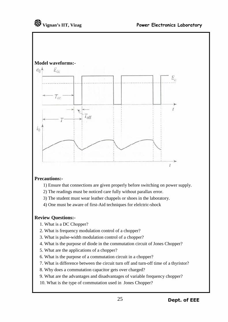
Observations:- Sample Calculations:- Eo = Edc * Ton / T
S.No Duty ratio Load voltage
Theoretical Practical
Vignan’s IIT, Vizag Power Electronics Laboratory
Dept. of EEE 25
Model waveforms:-
Precautions:- 1) Ensure that connections are given properly before switching on power supply.
2) The readings must be noticed care fully without parallax error.
3) The student must wear leather chappels or shoes in the laboratory.
4) One must be aware of first-Aid techniques for elelctric-shock
Review Questions:- 1. What is a DC Chopper?
2. What is frequency modulation control of a chopper?
3. What is pulse-width modulation control of a chopper?
4. What is the purpose of diode in the commutation circuit of Jones Chopper?
5. What are the applications of a chopper?
6. What is the purpose of a commutation circuit in a chopper?
7. What is difference between the circuit turn off and turn-off time of a thyristor?
8. Why does a commutation capacitor gets over charged?
9. What are the advantages and disadvantages of variable frequency chopper?
10. What is the type of commutation used in Jones Chopper?
Vignan’s IIT, Vizag Power Electronics Laboratory
Dept. of EEE 26
11. What is the principle of operation of step down and step up chopper? Results:-
1-� PARALLEL INVERTER
Aim:- To study the principle of operation of single Phase parallel inverter with R and RL- Loads and Observe the variation in the load voltage.
Apparatus:- Sl. No Item Type / Range Quantity
1. Parallel inverter power
circuit
300V/2A 1N0
2. Parallel inverter firing
circuit
2V/200mA 1No
3. Regulated Power supply, 30 volts/ 2Amps 1No
4. C.R.O. - 1No
5. Rheostat 50 ohm/2A 1No
6. Inductor 150mH/2A 1No
7. Connecting wires 5A
Theory:-
This circuit is typical class ‘C’ Parallel Inverter . Assume TN to be ON and Tp to be OFF. The lower end of the commutating capacitor is charged to twice the supply voltage and remains at this value until Tp is turned on. When Tp is turned on, The current flows through lower half of the primary, Tp and commutation inductance (L), Since the voltage across C cannot be instantaneous, the common SCR cathode point raises approximately to 2V dc and reverse biases TN. Thus TN turns off and C discharges through L, the supply circuit and then recharges in the reverse direction. The autotransformer action makes C to charge making now its upper point to reach +2V dc volts ready to commutate Tp, when TN is again turned on and the cycle repeats. The major purpose of commutation inductor (L) is to limit commutation capacitor charging current during switching.
Free wheeling diodes Dp and DN assist the inverter in handling a wide range of loads
and the value of C may be reduced since the capacitor now does not have to carry the reactive
Exp. - 7

Vignan’s IIT, Vizag Power Electronics Laboratory
Dept. of EEE 27
current. To dampen the feedback diode currents with in the half period, feed back diodes are connected to tapping of the transformer of 25V.
Circuit Diagram:-
L
D1
D2
SCR2
CKV L
RL
+
-
VDC
SCR1
Procedure:-
1. Switch on the inverter firing circuit and check the trigger output signal TP and
TN by varying frequency pot and by operating ON/OFF switch.
2. Connect the power supply, inverter power circuit, inverter firing circuit and load as
per circuit diagram.
3. Switch ON the 30V DC supply to the inverter power circuit.
4. Switch ON the 1-Ф, 230V 50Hz input supply of inverter firing circuit.
5. Apply main SCR trigger pulses by pressing ON/OFF switch to ON position.
6. Observe the output voltage waveform across load on CRO
7. Observe the output voltage by varying the switching frequency of the inverter
8. After completion of experiment first switch OFF 30V DC supply to power circuit then
switch OFF the trigger pulses.
Vignan’s IIT, Vizag Power Electronics Laboratory
Dept. of EEE 28
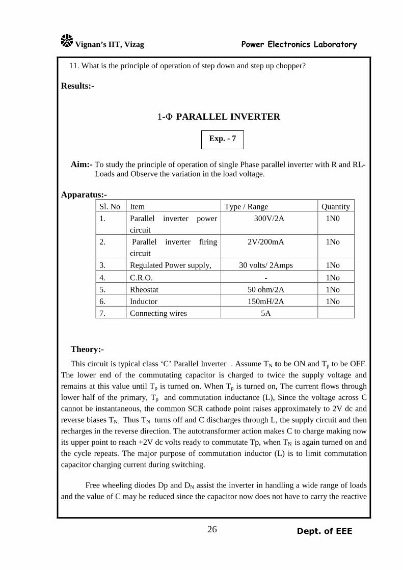
Model Waveforms:-
Precautions:-
1.To Switch OFF the inverter switch off DC input supply only. Switching off of the
trigger pulses will lead to short circuit.
2. Ensure that connections are given properly before switching on the power supply.
3. The readings must be noticed care fully without parallax error.
4. One must be aware of first-Aid techniques for electric-shock
Review Questions:-
1.What type of commutation is used in parallel Inverter ? 2. Why the name parallel ?
3. What is the shape of the output voltage wave form of Parallel Inverter? Why it is
so?
4.What is the minimum and maximum frequency of output voltage in this parallel inverter?
Results:

Vignan’s IIT, Vizag Power Electronics Laboratory
Dept. of EEE 29
1-φ CYCLO-CONVERTER
Aim:- To study the output voltage wave forms of a Single Phase Cyclo-Converter with R and RL loads
Apparatus:-
S.No Item Type & Range Quantity 1. l - � Isolation
Transformer 230/230V,1KVA 1 No
2. 1 -�cyclo-converter Power circuit
230V,5A 1NO
3. 1-� Cyclo-converter firing circuit
5V,200mA 1NO
4. Resistance 50ohm/5A 1 NO
5. CRO - 1 NO 6. Attenuation probe 10:1 1 NO
Theory:-
Circuit diagram:-
T1
T3
T4
T2
VS R-LOAD230V,50Hz
AC
Exp. - 8
Vignan’s IIT, Vizag Power Electronics Laboratory
Dept. of EEE 30
Procedure:-
1.Switch ON micro controlled based firing circuit and check the firing pulses of
deferent SCR’S.
2.Connect Cyclo converter Power circuit, Firing circuit and load as per the circuit
diagram.
3.Give 1- Ф, 230V 50Hz ac SUPPLY TO POWER CIRCUIT BY CLOSING dpst
SWITCH.
4.switch ON power supply to firing circuit
5.Set frequency division , firing angle keeping ON/OFF button on OFF state.
6.Apply firing pulses to SCR’s by keeping ON/OFF button in ON state.
7.Observe the output voltage waveform on CRO for the specified frequency.
8.Repeat SNO. 7 for different frequency divisions.
9.After completion of experiment switch OFF power circuit first that firing circuit.
Note:- If the out put shows zero even after making the connections properly, switch off the
input supply and inter change the input supply. This is to make the input supply to the
firing unit and the power circuit in the same phase. If they are just opposite in phase,
none of the SCRs will trigger and output will be zero.
Observations:-
S.No Input voltage, Vin Firing Angle Load current, IL Load voltage VL

Vignan’s IIT, Vizag Power Electronics Laboratory
Dept. of EEE 31
Model Wave forms:-
Precautions:-
1) Ensure that connections are given properly before switching on the power supply.
2) The readings must be noticed care fully without parallax error.
3) One must be aware of first-Aid techniques for electric-shock
4) ) Always change the frequency division only after switching off the trigger output
Review Questions:-
1.Explain working principle of cyclo-converter?
2.What type of commutation is used in cyclo-converter?
3.What happens to the out put if the frequency of operation is beyond suggested limit?
4. What is the major difference between an AC voltage controller and a cyclo-
converter?
Results:

Vignan’s IIT, Vizag Power Electronics Laboratory
Dept. of EEE 32
l-� HALF-CONTROLLED BRIDGE CONVERTER
Aim:- To study the operation of a single phase half controlled converter.
Apparatus:-
Theory:-
Circuit diagram:-
230V,50HzAC
T1T2
D1 D2
Dm
R
L
V0
s. no Item Type & Range Quantity
1.
l-� Isolation Transformer
230/230V,1KVA 1No
2. Half Converter power circuit
230V/5A 1 No
3. Half converter Firing circuit
5V,200mA 1 No
4. Resistor 50ohm,5A 1 No
5. Inductor 150mH,2A 1 No
6. Ammeter 0-5A,M.C 1 No
7. Voltmeter 0-300V,M.C 1No
8. CRO - 1No
9. Attenuation Probes 10:1 1NO
Exp. - 9

Vignan’s IIT, Vizag Power Electronics Laboratory
Dept. of EEE 33
Procedure:-
1.Switch On firing circuit and check the firing pulses.
2. Connect the power circuit, firing circuit, Load as per the circuit diagram.
3. Give 1-Ф, 230V 50HZ supply to the power circuit by closing DPST switch.
4. Switch on firing pulses to SCR s by keeping ON/OFF soft switch in ON position.
5. Observe the load voltage Wave and current Wave (using shunt element of 1 ohm)
6.Record load voltage and current by varying firing angle of SR from voltmeter and
ammeter.
7.After completion of experiment switch OFF power circuit first then firing circuit.
8. Plot the graph between firing angle and output voltage. Observations:-
S.No Input voltage, Vin Firing Angle Load current, IL Load voltage VL Practical Theoretical
Sample Calculations:-
The average output can be found from )(2
2wtSinwtdVmVo ∫=
π
απ= Vm (1+cos α) / п
I0 = Vo/R Model waveforms:-

Vignan’s IIT, Vizag Power Electronics Laboratory
Dept. of EEE 34
Precautions:- 1. Don't touch the rectifier output terminals when the power card of the power circuit is inserted in.
2. Ensure that connections are given properly before switching on the power supply.
3. The readings must be noticed care fully without parallax error.
4. One must be aware of first-Aid techniques for electric-shock
Review Questions :-
1. What are the advantages of semi converter over full converter?
2. What is the effect of freewheeling diode in Half-Controlled converter?
3. What is meant by one quadrant operation of converters?
4. Which converter gives two quadrant operation?
5. Sketch the load voltage and current wave forms for Semi- converter with RL load? Result:

Vignan’s IIT, Vizag Power Electronics Laboratory
Dept. of EEE 35
1-Ф SERIES INVERTER WITH R AND RL LOADS
Aim:- To observe the effect of variation of trigger frequency on output voltage of a series
inverter
Apparatus:-
Name Plate details: - SCR TYN 612, 12A/600V, Diodes BYW51-200 4A/200V. C1 6.8 µ Farad /100V, C2 6.8 µ Farad /100V, L I 5mH/2A, L2 10mH/2A.
Theory:-
Circuit diagram:-
LOAD
T1
T2
L
L
D1
D2
FUSE
MCB
C1 (C2)
C1(C2)
S.NO Item Type/Range Quantity
1. Modified Series inverter kit 1 No 2. C.R.O. With Probe - 1No 3. Connecting wires Adequate 4. DC Regulated power supply 0-30 Volts ,2A. 1No
5. Rheostat 50mH/2A 1No
6. Inductor with tapping 50mH/2A 1NO
Exp. - 10
Vignan’s IIT, Vizag Power Electronics Laboratory
Dept. of EEE 36
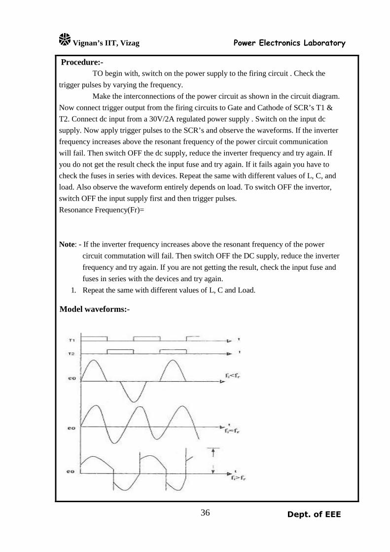
Procedure:- TO begin with, switch on the power supply to the firing circuit . Check the
trigger pulses by varying the frequency.
Make the interconnections of the power circuit as shown in the circuit diagram.
Now connect trigger output from the firing circuits to Gate and Cathode of SCR’s T1 &
T2. Connect dc input from a 30V/2A regulated power supply . Switch on the input dc
supply. Now apply trigger pulses to the SCR’s and observe the waveforms. If the inverter
frequency increases above the resonant frequency of the power circuit communication
will fail. Then switch OFF the dc supply, reduce the inverter frequency and try again. If
you do not get the result check the input fuse and try again. If it fails again you have to
check the fuses in series with devices. Repeat the same with different values of L, C, and
load. Also observe the waveform entirely depends on load. To switch OFF the invertor,
switch OFF the input supply first and then trigger pulses.
Resonance Frequency(Fr)=
Note: - If the inverter frequency increases above the resonant frequency of the power
circuit commutation will fail. Then switch OFF the DC supply, reduce the inverter
frequency and try again. If you are not getting the result, check the input fuse and
fuses in series with the devices and try again.
1. Repeat the same with different values of L, C and Load. Model waveforms:-

Vignan’s IIT, Vizag Power Electronics Laboratory
Dept. of EEE 37
Precautions:-
1. Ensure that connections are given properly before switching on the power supply.
2. Use unearthed Oscilloscope
Review questions:- 1. What is an inverter?
2. What is the basic principle of Series inverter?
3. What type of commutation is used in Series Inverter?
4. Why Inverter output is not pure sinusoidal? Result: