afe5851 16-channel variable gain ampl w/octal high-speed
TRANSCRIPT
User's GuideSLOU258C–March 2009–Revised March 2015
AFE5851 16-Channel Variable Gain Amplifier (VGA) withOctal High-Speed ADC
The AFE5851EVM is an evaluation tool designed for the ultrasound analog front-end (AFE) deviceAFE5851. In order to deserialize the outputs of AFE5851, an ADSDeSer-50EVM or TSW1400EVM isneeded during the evaluation.
Contents1 Introduction ................................................................................................................... 3
1.1 AFE5851EVM Kit Contents........................................................................................ 51.2 Features.............................................................................................................. 51.3 Power Supplies ..................................................................................................... 51.4 Indicators............................................................................................................. 6
2 Board Configuration ......................................................................................................... 82.1 Board Connections Overview ..................................................................................... 92.2 I/O and Power Connectors ....................................................................................... 102.3 Jumpers and Setup ............................................................................................... 102.4 Test Points ......................................................................................................... 11
3 Board Operation ............................................................................................................ 113.1 Software Installation and Operation ............................................................................ 123.2 USB Driver Installation ........................................................................................... 123.3 GUI Startup ........................................................................................................ 143.4 Hardware Setup ................................................................................................... 173.5 Clock Selection .................................................................................................... 183.6 Data Analysis ...................................................................................................... 18
4 Schematics, Layout and Bill of Materials................................................................................ 194.1 Schematics ......................................................................................................... 194.2 PCB Layout ........................................................................................................ 254.3 Bill of Materials .................................................................................................... 34
5 Typical Performance ....................................................................................................... 37Appendix A TSW1400 for Evaluating AFE5851 ............................................................................. 39Appendix B High Speed Data Converter Pro (HSDCPro) GUI Installation .............................................. 52
List of Figures
1 AFE5851 Block Diagram.................................................................................................... 42 Block Diagram of Test Setup............................................................................................... 53 AFE5851EVM LED Locations.............................................................................................. 64 AFE5851EVM Top and Bottom Views .................................................................................... 95 Locations of Jumpers, Headers and Switches on the AFE5851EVM ............................................... 106 Default Setup for Jumpers ................................................................................................ 117 AFE5851EVM USB SPI Interface for General Registers ............................................................. 148 AFE5851EVM USB SPI Fixed Gain Mode.............................................................................. 159 AFE5851EVM USB SPI Interface for Variable Gain Mode ........................................................... 1610 Typical AFE5851 Bench Setup ........................................................................................... 1711 Clock selection jumper configurations: (a) Transformer (default); (b) Single-ended clock; (c) Future CLK
input option based on U1. Both (b) and (c) configurations need some modifications on the PCB. ............. 18
1SLOU258C–March 2009–Revised March 2015 AFE5851 16-Channel Variable Gain Amplifier (VGA) with Octal High-SpeedADCSubmit Documentation Feedback
Copyright © 2009–2015, Texas Instruments Incorporated
www.ti.com
12 Schematic Page 1.......................................................................................................... 1913 Schematic Page 2.......................................................................................................... 2014 Schematic Page 3.......................................................................................................... 2115 Schematic Page 4.......................................................................................................... 2216 Schematic Page 5.......................................................................................................... 2317 Schematic Page 6.......................................................................................................... 2418 Top Layer – Signal ......................................................................................................... 2619 Inner Layer 1 – Ground.................................................................................................... 2720 Inner Layer 2 – Signal ..................................................................................................... 2821 Inner Layer 3 – Power ..................................................................................................... 2922 Inner Layer 4 – Ground.................................................................................................... 3023 Bottom Layer – Signal ..................................................................................................... 3124 Top Silk Screen Layer ..................................................................................................... 3225 Bottom Silk Screen Layer ................................................................................................. 3326 Typical Performance of AFE5851 — (a) Fixed Gain Mode; (b) Variable Gain Mode ............................. 3827 Connection Between TSW1400EVM and AFE5851................................................................... 3928 Connecting the Instruments............................................................................................... 4029 AFE5851 EVM GUI –Run Mode ......................................................................................... 4130 AFE5851 EVM GUI – START Button.................................................................................... 4231 AFE5851 EVM GUI – Variable Gain..................................................................................... 4332 AFE5851 EVM GUI – Setting Fixed Gain ............................................................................... 4433 User Interface: Initial Setup Screen...................................................................................... 4534 User Interface: Step-by-Step Setup...................................................................................... 4635 User Interface: Frequency Load Value to Signal Generator.......................................................... 4736 User Interface: Final Setup Screen ...................................................................................... 4837 User Interface: Single FFT Format....................................................................................... 4938 User Interface: Time Domain Format.................................................................................... 5039 Plot of Saved Sample Data ............................................................................................... 5140 HSDCPro Install (Begin)................................................................................................... 5241 HSDCPro Install (Install Directory) ....................................................................................... 5342 HSDCPro Install (TI License Agreement) ............................................................................... 5443 HSDCPro Install (NI License Agreement)............................................................................... 5544 HSDCPro Install (Start Installation) ...................................................................................... 5645 HSDCPro Install (Installation Progress) ................................................................................. 5746 HSDCPro Install (Installation Complete) ................................................................................ 5847 HSDCPro Install (h) ........................................................................................................ 5948 HSDCPro Install ............................................................................................................ 59
List of Tables
1 Channel to Channel Matching Between the AFE5851EVM and ADSDeSER-50EVM ........................... 17
2 AFE5851 16-Channel Variable Gain Amplifier (VGA) with Octal High-Speed SLOU258C–March 2009–Revised March 2015ADC Submit Documentation Feedback
Copyright © 2009–2015, Texas Instruments Incorporated
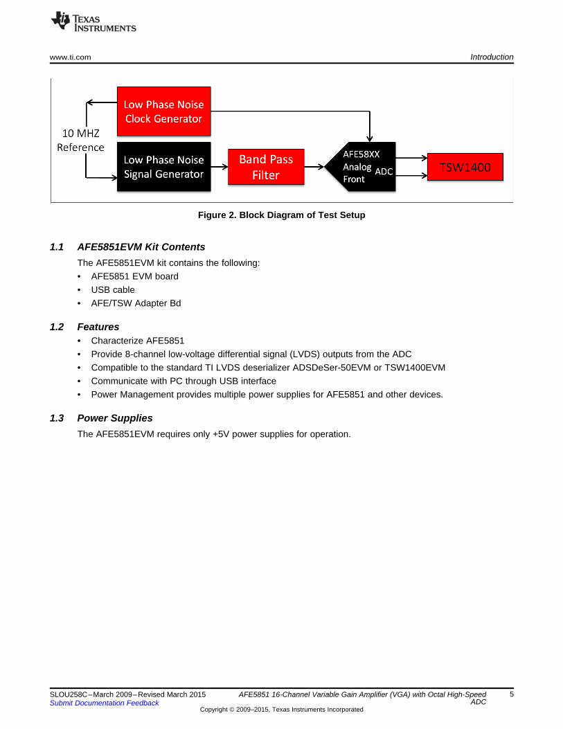
www.ti.com Introduction
1 IntroductionThe AFE5851 includes an 16-channel Voltage-Controlled-Amplifier (VCA) with digital control and an 8-channel 65MSPS analog-to-digital converter (ADC). The 16 analog input signals will be processed by theanalog front-end circuit of AFE5851; the outputs of the analog front-end will then be digitalized by the ADCwithin the device. There are only eight ADCs within the AFE5851; therefore the odd and even channelsare multiplexed into one LVDS output pair. The output of the ADC is streamed out in serial format. In orderto process the sample data, the Texas Instruments' TSW1400EVM is recommended. The TSW1400includes a High-Speed LVDS Deserializer, Demultiplexer, and Analysis System which provide acomprehensive set of hardware and user interface software to effectively evaluate the performance ofAFE5851.
3SLOU258C–March 2009–Revised March 2015 AFE5851 16-Channel Variable Gain Amplifier (VGA) with Octal High-SpeedADCSubmit Documentation Feedback
Copyright © 2009–2015, Texas Instruments Incorporated

AAF
VCA1
IN1
AAF
VCA2
IN2
AAF
VCA3
IN3
AAF
VCA4
IN4
AAF
VCA15
IN15
AAF
VCA16
IN16
ADC 1 SERIALIZER
LVDS
D1PD1M
ADC 2 SERIALIZERD2PD2M
ADC 8 SERIALIZERD8PD8M
AVDD3
AVDD18
CLKINP
CLKINM
TIME GAIN BLOCK
CONTLOL
MEMORYSERIAL
INTERFACE
TIME GAINCurve 1
TIME GAINCurve 2
TIME GAINCurve 3
LVDD18
TG
C S
YN
C
PD
N
SC
LK
SD
ATA
SE
N
RE
SE
T
SD
OU
T
fCLKIN
fADC
Clock Divider(by 2)
PLL6X fCLKIN
fCLKIN/2
FRAME CLOCK
BIT CLOCK
FCLKPFCLKM
DCLKP
DCLKM
Introduction www.ti.com
Figure 1. AFE5851 Block Diagram
4 AFE5851 16-Channel Variable Gain Amplifier (VGA) with Octal High-Speed SLOU258C–March 2009–Revised March 2015ADC Submit Documentation Feedback
Copyright © 2009–2015, Texas Instruments Incorporated
www.ti.com Introduction
Figure 2. Block Diagram of Test Setup
1.1 AFE5851EVM Kit ContentsThe AFE5851EVM kit contains the following:• AFE5851 EVM board• USB cable• AFE/TSW Adapter Bd
1.2 Features• Characterize AFE5851• Provide 8-channel low-voltage differential signal (LVDS) outputs from the ADC• Compatible to the standard TI LVDS deserializer ADSDeSer-50EVM or TSW1400EVM• Communicate with PC through USB interface• Power Management provides multiple power supplies for AFE5851 and other devices.
1.3 Power SuppliesThe AFE5851EVM requires only +5V power supplies for operation.
5SLOU258C–March 2009–Revised March 2015 AFE5851 16-Channel Variable Gain Amplifier (VGA) with Octal High-SpeedADCSubmit Documentation Feedback
Copyright © 2009–2015, Texas Instruments Incorporated
Introduction www.ti.com
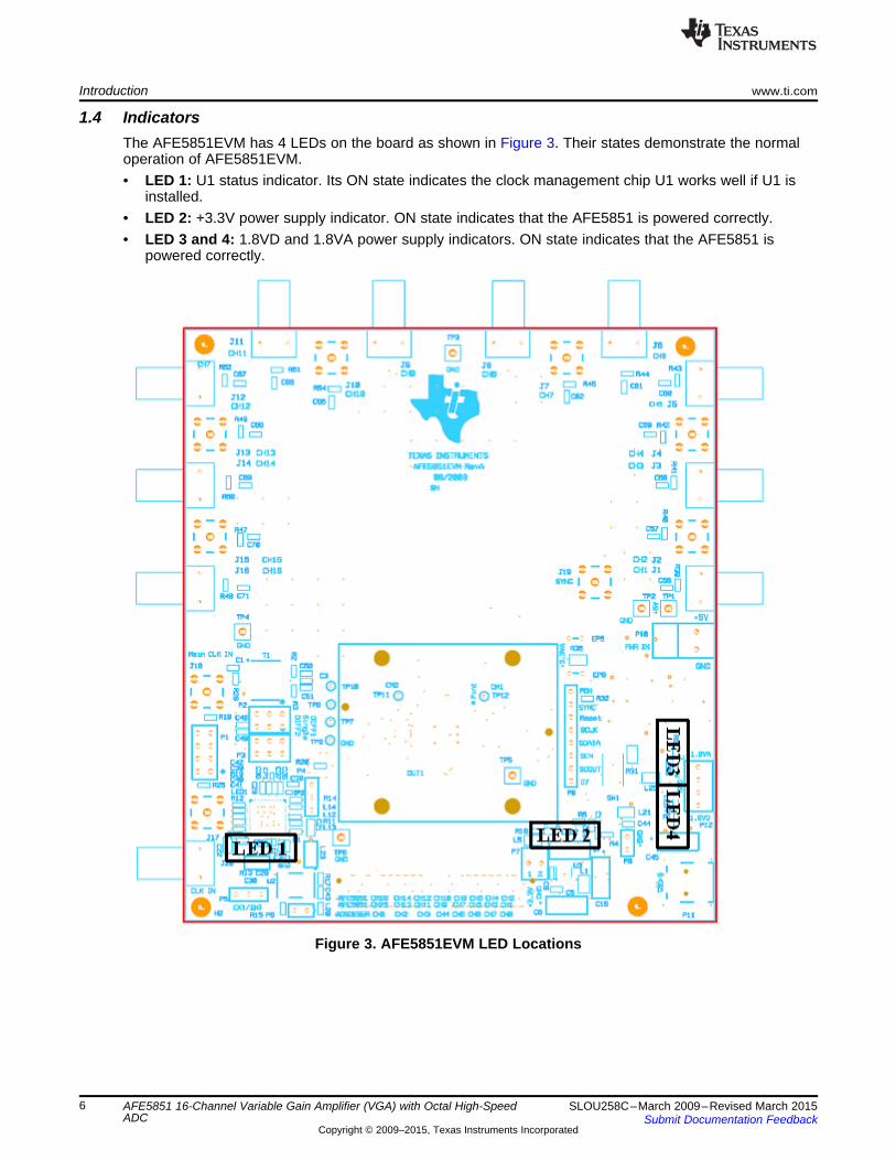
1.4 IndicatorsThe AFE5851EVM has 4 LEDs on the board as shown in Figure 3. Their states demonstrate the normaloperation of AFE5851EVM.• LED 1: U1 status indicator. Its ON state indicates the clock management chip U1 works well if U1 is
installed.• LED 2: +3.3V power supply indicator. ON state indicates that the AFE5851 is powered correctly.• LED 3 and 4: 1.8VD and 1.8VA power supply indicators. ON state indicates that the AFE5851 is
powered correctly.
Figure 3. AFE5851EVM LED Locations
6 AFE5851 16-Channel Variable Gain Amplifier (VGA) with Octal High-Speed SLOU258C–March 2009–Revised March 2015ADC Submit Documentation Feedback
Copyright © 2009–2015, Texas Instruments Incorporated
www.ti.com Introduction
7SLOU258C–March 2009–Revised March 2015 AFE5851 16-Channel Variable Gain Amplifier (VGA) with Octal High-SpeedADCSubmit Documentation Feedback
Copyright © 2009–2015, Texas Instruments Incorporated

Board Configuration www.ti.com
2 Board ConfigurationThis chapter describes the locations and functionalities of inputs, outputs, jumpers, test points of theAFE5851EVM in detail.
8 AFE5851 16-Channel Variable Gain Amplifier (VGA) with Octal High-Speed SLOU258C–March 2009–Revised March 2015ADC Submit Documentation Feedback
Copyright © 2009–2015, Texas Instruments Incorporated
www.ti.com Board Configuration
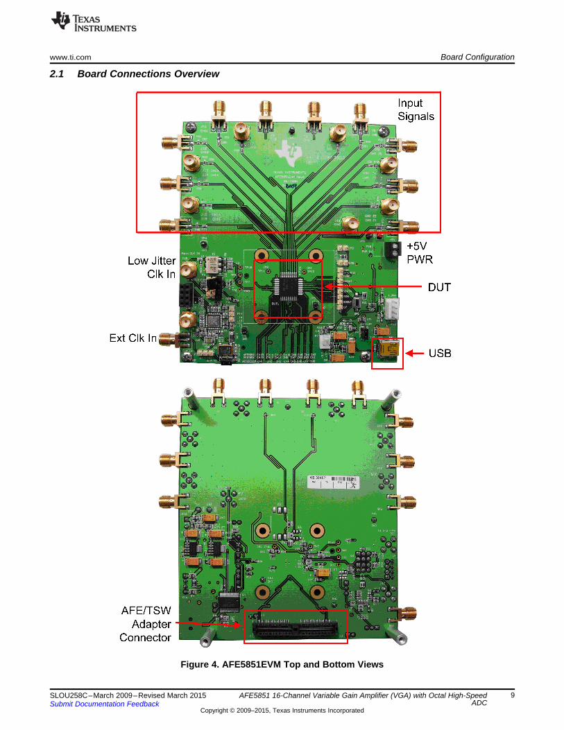
2.1 Board Connections Overview
Figure 4. AFE5851EVM Top and Bottom Views
9SLOU258C–March 2009–Revised March 2015 AFE5851 16-Channel Variable Gain Amplifier (VGA) with Octal High-SpeedADCSubmit Documentation Feedback
Copyright © 2009–2015, Texas Instruments Incorporated
Board Configuration www.ti.com
2.2 I/O and Power ConnectorsThe positions and functions of the AFE5851EVM connectors are discussed in this section.• Analog Inputs Ch1~Ch16 (J1~J16): Single-end analog signals.• Low Jitter CLK Source Input (J18): This input accepts clocks with low jitter noise, such as HP8644
output. 20~65MHz 50% duty cycle clock with 1~2Vrms amplitude can be used. When J18 is used,make sure shunt P4,5,6 are removed.
• CLK output (J17): The output of either the U1 output or the on-board 40MHz oscillator outputdepending on jumper P4’s connection.
• External CLK Input (J20): ADC Clock input, such as FPGA outputs. FPGA outputs must be processedby U1. Otherwise, the ADC of AFE5851 will not achieve satisfactory SNR performance.
• +5V PWR connector(P10): Power supply input• USB input (P11): USB interface to control the AFE5851.• LVDS Outputs Ch1~Ch8 (P13): Differential LVDS data outputs.
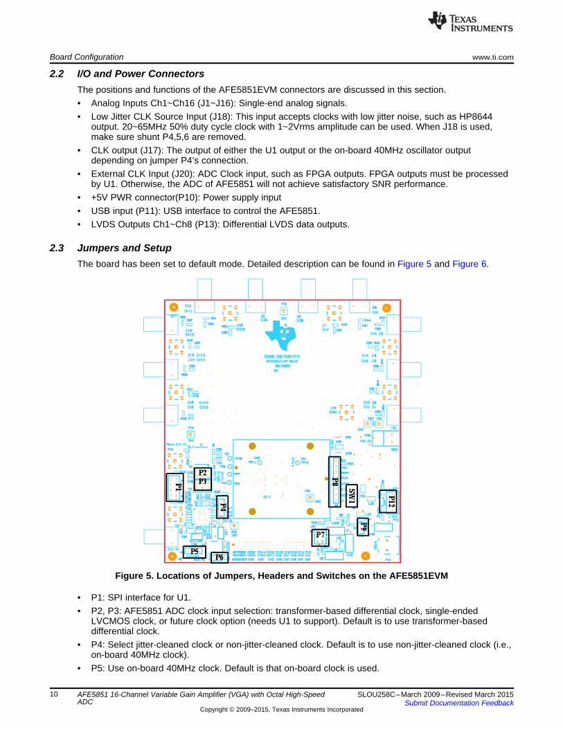
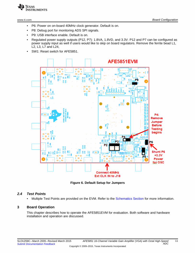
2.3 Jumpers and SetupThe board has been set to default mode. Detailed description can be found in Figure 5 and Figure 6.
Figure 5. Locations of Jumpers, Headers and Switches on the AFE5851EVM
• P1: SPI interface for U1.• P2, P3: AFE5851 ADC clock input selection: transformer-based differential clock, single-ended
LVCMOS clock, or future clock option (needs U1 to support). Default is to use transformer-baseddifferential clock.
• P4: Select jitter-cleaned clock or non-jitter-cleaned clock. Default is to use non-jitter-cleaned clock (i.e.,on-board 40MHz clock).
• P5: Use on-board 40MHz clock. Default is that on-board clock is used.
10 AFE5851 16-Channel Variable Gain Amplifier (VGA) with Octal High-Speed SLOU258C–March 2009–Revised March 2015ADC Submit Documentation Feedback
Copyright © 2009–2015, Texas Instruments Incorporated
www.ti.com Board Configuration
• P6: Power on on-board 40MHz clock generator. Default is on.• P8: Debug port for monitoring ADS SPI signals.• P9: USB interface enable. Default is on.• Regulated power supply outputs (P12, P7): 1.8VA, 1.8VD, and 3.3V. P12 and P7 can be configured as
power supply input as well if users would like to skip on board regulators. Remove the ferrite bead L1,L2, L3, L7 and L24,
• SW1: Reset switch for AFE5851.
Figure 6. Default Setup for Jumpers
2.4 Test Points• Multiple Test Points are provided on the EVM. Refer to the Schematics Section for more information.
3 Board OperationThis chapter describes how to operate the AFE5851EVM for evaluation. Both software and hardwareinstallation and operation are discussed.
11SLOU258C–March 2009–Revised March 2015 AFE5851 16-Channel Variable Gain Amplifier (VGA) with Octal High-SpeedADCSubmit Documentation Feedback
Copyright © 2009–2015, Texas Instruments Incorporated
Board Operation www.ti.com
3.1 Software Installation and OperationThe AFE5851EVM comes with a software install. To Dowload the software, visit the AFE5851 productfolder and select Tools & software . Once the zip folder is downloaded, run setup.exe to install thesoftware. The software to use the TSW1400EVM is called HSDCPro (High Speed Data Converter Pro).For information on how to download this software, please see Appendix B.
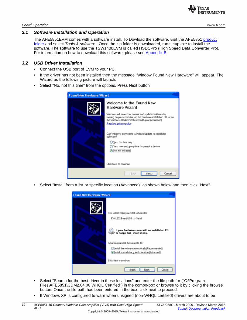
3.2 USB Driver Installation• Connect the USB port of EVM to your PC.• If the driver has not been installed then the message “Window Found New Hardware” will appear. The
Wizard as the following picture will launch.• Select "No, not this time" from the options. Press Next button
• Select "Install from a list or specific location (Advanced)" as shown below and then click "Next".
• Select "Search for the best driver in these locations" and enter the file path for ("C:\ProgramFiles\AFE5851\CDM2.04.06 WHQL Certified") in the combo-box or browse to it by clicking the browsebutton. Once the file path has been entered in the box, click next to proceed.
• If Windows XP is configured to warn when unsigned (non-WHQL certified) drivers are about to be
12 AFE5851 16-Channel Variable Gain Amplifier (VGA) with Octal High-Speed SLOU258C–March 2009–Revised March 2015ADC Submit Documentation Feedback
Copyright © 2009–2015, Texas Instruments Incorporated
www.ti.com Board Operation
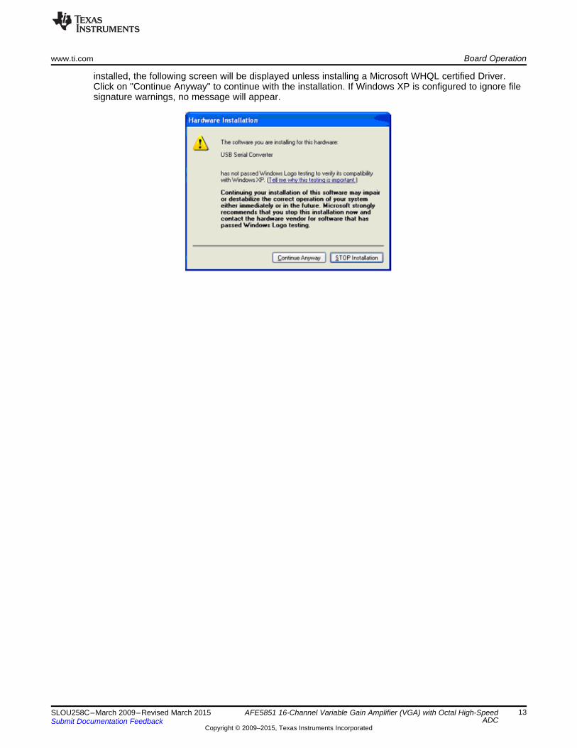
installed, the following screen will be displayed unless installing a Microsoft WHQL certified Driver.Click on "Continue Anyway" to continue with the installation. If Windows XP is configured to ignore filesignature warnings, no message will appear.
13SLOU258C–March 2009–Revised March 2015 AFE5851 16-Channel Variable Gain Amplifier (VGA) with Octal High-SpeedADCSubmit Documentation Feedback
Copyright © 2009–2015, Texas Instruments Incorporated
Board Operation www.ti.com
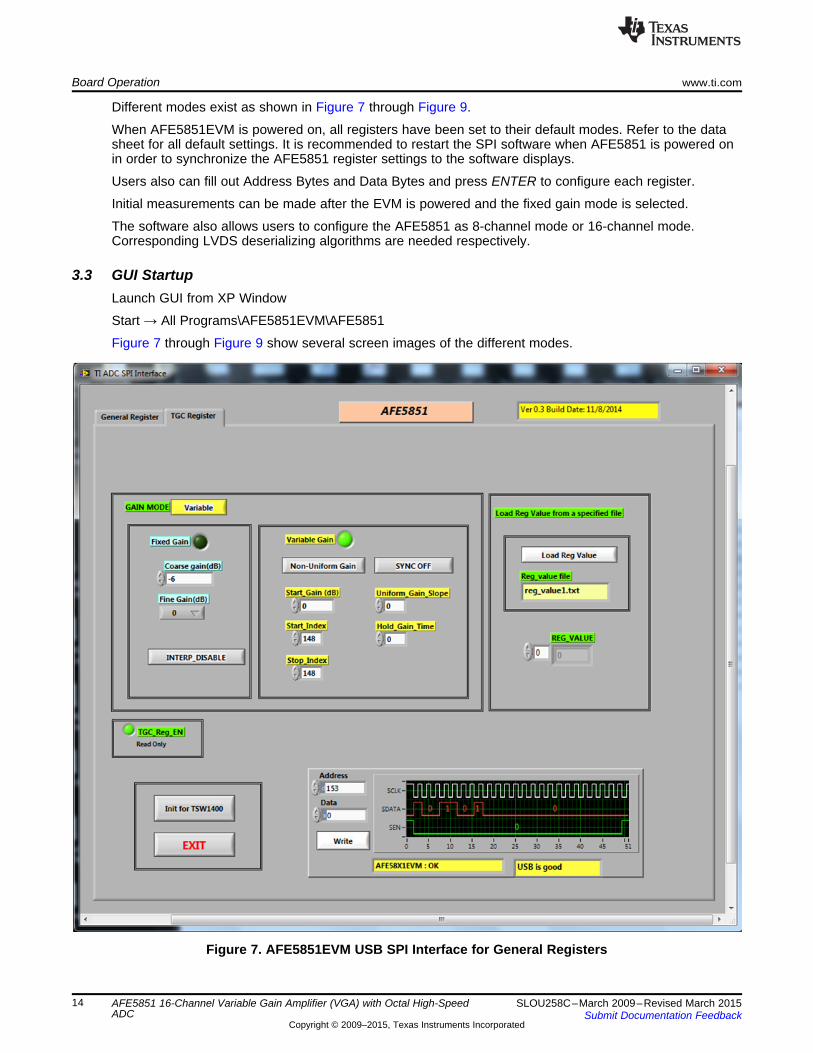
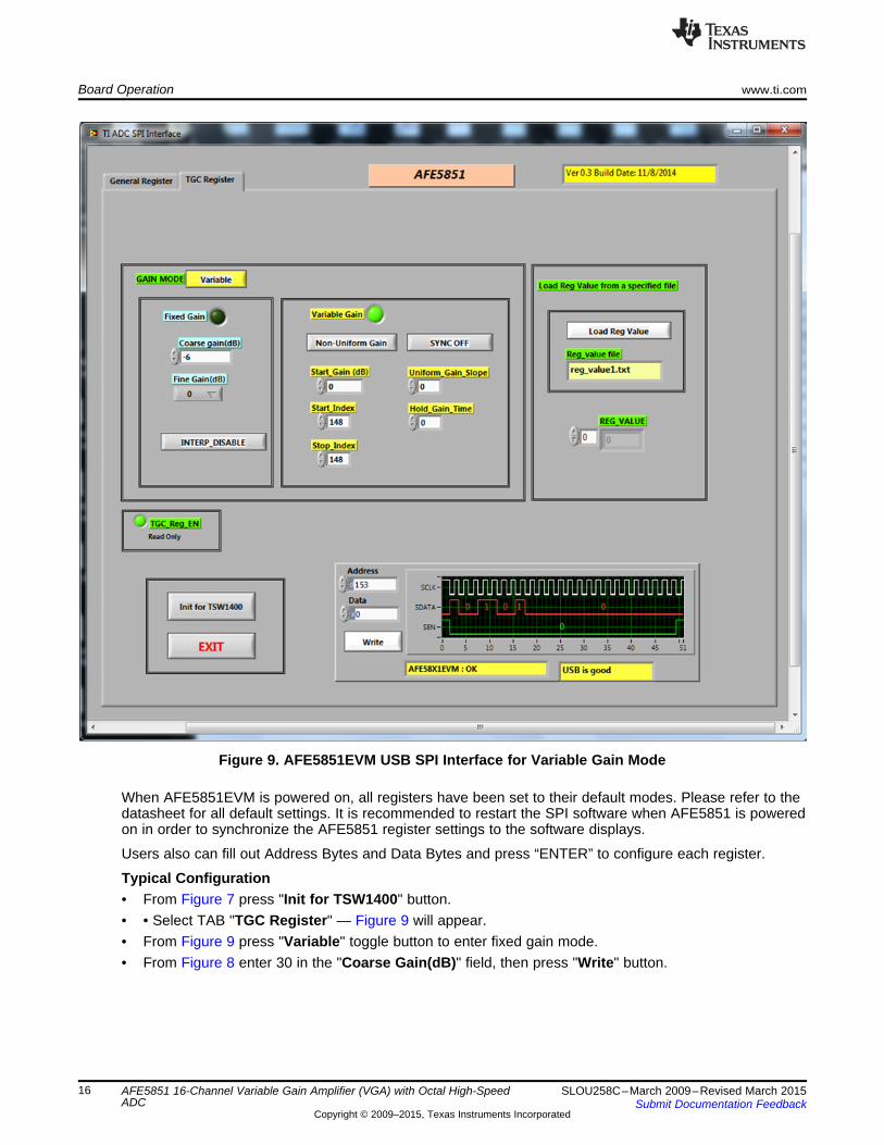
Different modes exist as shown in Figure 7 through Figure 9.
When AFE5851EVM is powered on, all registers have been set to their default modes. Refer to the datasheet for all default settings. It is recommended to restart the SPI software when AFE5851 is powered onin order to synchronize the AFE5851 register settings to the software displays.
Users also can fill out Address Bytes and Data Bytes and press ENTER to configure each register.
Initial measurements can be made after the EVM is powered and the fixed gain mode is selected.
The software also allows users to configure the AFE5851 as 8-channel mode or 16-channel mode.Corresponding LVDS deserializing algorithms are needed respectively.
3.3 GUI StartupLaunch GUI from XP Window
Start → All Programs\AFE5851EVM\AFE5851
Figure 7 through Figure 9 show several screen images of the different modes.
Figure 7. AFE5851EVM USB SPI Interface for General Registers
14 AFE5851 16-Channel Variable Gain Amplifier (VGA) with Octal High-Speed SLOU258C–March 2009–Revised March 2015ADC Submit Documentation Feedback
Copyright © 2009–2015, Texas Instruments Incorporated

www.ti.com Board Operation
Figure 8. AFE5851EVM USB SPI Fixed Gain Mode
15SLOU258C–March 2009–Revised March 2015 AFE5851 16-Channel Variable Gain Amplifier (VGA) with Octal High-SpeedADCSubmit Documentation Feedback
Copyright © 2009–2015, Texas Instruments Incorporated
Board Operation www.ti.com
Figure 9. AFE5851EVM USB SPI Interface for Variable Gain Mode
When AFE5851EVM is powered on, all registers have been set to their default modes. Please refer to thedatasheet for all default settings. It is recommended to restart the SPI software when AFE5851 is poweredon in order to synchronize the AFE5851 register settings to the software displays.
Users also can fill out Address Bytes and Data Bytes and press “ENTER” to configure each register.
Typical Configuration• From Figure 7 press "Init for TSW1400" button.• • Select TAB "TGC Register" — Figure 9 will appear.• From Figure 9 press "Variable" toggle button to enter fixed gain mode.• From Figure 8 enter 30 in the "Coarse Gain(dB)" field, then press "Write" button.
16 AFE5851 16-Channel Variable Gain Amplifier (VGA) with Octal High-Speed SLOU258C–March 2009–Revised March 2015ADC Submit Documentation Feedback
Copyright © 2009–2015, Texas Instruments Incorporated
www.ti.com Board Operation
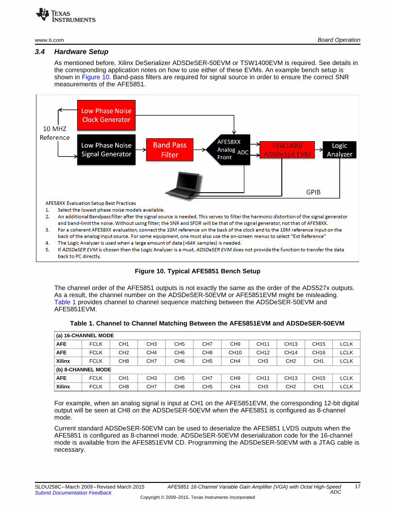
3.4 Hardware SetupAs mentioned before, Xilinx DeSerializer ADSDeSER-50EVM or TSW1400EVM is required. See details inthe corresponding application notes on how to use either of these EVMs. An example bench setup isshown in Figure 10. Band-pass filters are required for signal source in order to ensure the correct SNRmeasurements of the AFE5851.
Figure 10. Typical AFE5851 Bench Setup
The channel order of the AFE5851 outputs is not exactly the same as the order of the ADS527x outputs.As a result, the channel number on the ADSDeSER-50EVM or AFE5851EVM might be misleading.Table 1 provides channel to channel sequence matching between the ADSDeSER-50EVM andAFE5851EVM.
Table 1. Channel to Channel Matching Between the AFE5851EVM and ADSDeSER-50EVM
(a) 16-CHANNEL MODEAFE FCLK CH1 CH3 CH5 CH7 CH9 CH11 CH13 CH15 LCLKAFE FCLK CH2 CH4 CH6 CH8 CH10 CH12 CH14 CH16 LCLKXilinx FCLK CH8 CH7 CH6 CH5 CH4 CH3 CH2 CH1 LCLK(b) 8-CHANNEL MODEAFE FCLK CH1 CH3 CH5 CH7 CH9 CH11 CH13 CH15 LCLKXilinx FCLK CH8 CH7 CH6 CH5 CH4 CH3 CH2 CH1 LCLK
For example, when an analog signal is input at CH1 on the AFE5851EVM, the corresponding 12-bit digitaloutput will be seen at CH8 on the ADSDeSER-50EVM when the AFE5851 is configured as 8-channelmode.
Current standard ADSDeSER-50EVM can be used to deserialize the AFE5851 LVDS outputs when theAFE5851 is configured as 8-channel mode. ADSDeSER-50EVM deserialization code for the 16-channelmode is available from the AFE5851EVM CD. Programming the ADSDeSER-50EVM with a JTAG cable isnecessary.
17SLOU258C–March 2009–Revised March 2015 AFE5851 16-Channel Variable Gain Amplifier (VGA) with Octal High-SpeedADCSubmit Documentation Feedback
Copyright © 2009–2015, Texas Instruments Incorporated
Board Operation www.ti.com
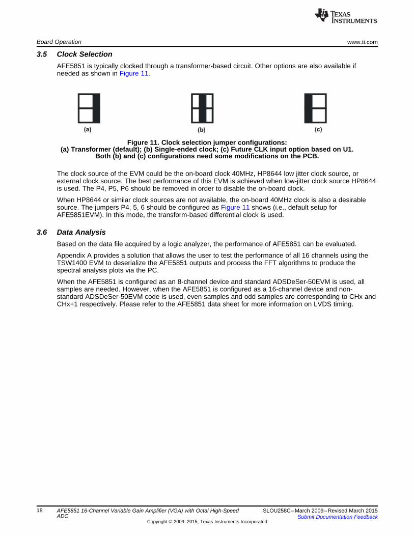
3.5 Clock SelectionAFE5851 is typically clocked through a transformer-based circuit. Other options are also available ifneeded as shown in Figure 11.
Figure 11. Clock selection jumper configurations:(a) Transformer (default); (b) Single-ended clock; (c) Future CLK input option based on U1.
Both (b) and (c) configurations need some modifications on the PCB.
The clock source of the EVM could be the on-board clock 40MHz, HP8644 low jitter clock source, orexternal clock source. The best performance of this EVM is achieved when low-jitter clock source HP8644is used. The P4, P5, P6 should be removed in order to disable the on-board clock.
When HP8644 or similar clock sources are not available, the on-board 40MHz clock is also a desirablesource. The jumpers P4, 5, 6 should be configured as Figure 11 shows (i.e., default setup forAFE5851EVM). In this mode, the transform-based differential clock is used.
3.6 Data AnalysisBased on the data file acquired by a logic analyzer, the performance of AFE5851 can be evaluated.
Appendix A provides a solution that allows the user to test the performance of all 16 channels using theTSW1400 EVM to deserialize the AFE5851 outputs and process the FFT algorithms to produce thespectral analysis plots via the PC.
When the AFE5851 is configured as an 8-channel device and standard ADSDeSer-50EVM is used, allsamples are needed. However, when the AFE5851 is configured as a 16-channel device and non-standard ADSDeSer-50EVM code is used, even samples and odd samples are corresponding to CHx andCHx+1 respectively. Please refer to the AFE5851 data sheet for more information on LVDS timing.
18 AFE5851 16-Channel Variable Gain Amplifier (VGA) with Octal High-Speed SLOU258C–March 2009–Revised March 2015ADC Submit Documentation Feedback
Copyright © 2009–2015, Texas Instruments Incorporated
www.ti.com Schematics, Layout and Bill of Materials
4 Schematics, Layout and Bill of MaterialsThis chapter provides the schematics and layout of the AFE5851EVM as well as the bill of materials.
4.1 Schematics
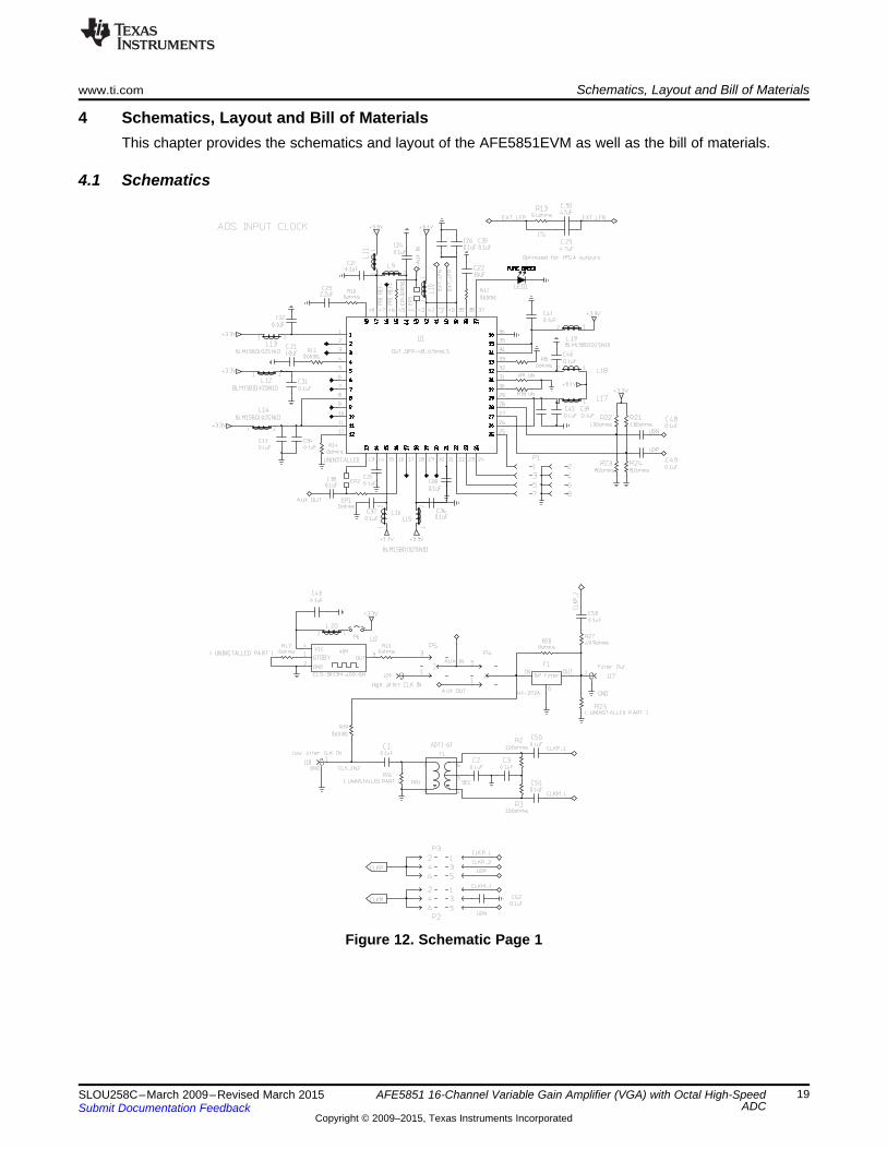
Figure 12. Schematic Page 1
19SLOU258C–March 2009–Revised March 2015 AFE5851 16-Channel Variable Gain Amplifier (VGA) with Octal High-SpeedADCSubmit Documentation Feedback
Copyright © 2009–2015, Texas Instruments Incorporated
Schematics, Layout and Bill of Materials www.ti.com
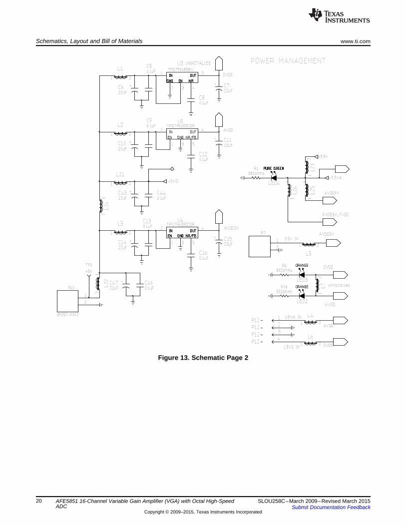
Figure 13. Schematic Page 2
20 AFE5851 16-Channel Variable Gain Amplifier (VGA) with Octal High-Speed SLOU258C–March 2009–Revised March 2015ADC Submit Documentation Feedback
Copyright © 2009–2015, Texas Instruments Incorporated
www.ti.com Schematics, Layout and Bill of Materials
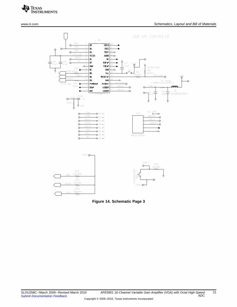
Figure 14. Schematic Page 3
21SLOU258C–March 2009–Revised March 2015 AFE5851 16-Channel Variable Gain Amplifier (VGA) with Octal High-SpeedADCSubmit Documentation Feedback
Copyright © 2009–2015, Texas Instruments Incorporated
Schematics, Layout and Bill of Materials www.ti.com
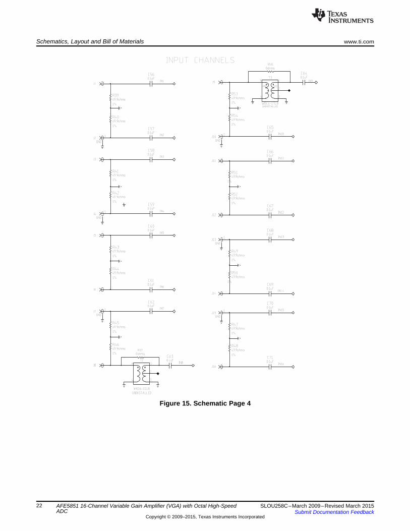
Figure 15. Schematic Page 4
22 AFE5851 16-Channel Variable Gain Amplifier (VGA) with Octal High-Speed SLOU258C–March 2009–Revised March 2015ADC Submit Documentation Feedback
Copyright © 2009–2015, Texas Instruments Incorporated

www.ti.com Schematics, Layout and Bill of Materials
Figure 16. Schematic Page 5
23SLOU258C–March 2009–Revised March 2015 AFE5851 16-Channel Variable Gain Amplifier (VGA) with Octal High-SpeedADCSubmit Documentation Feedback
Copyright © 2009–2015, Texas Instruments Incorporated

Schematics, Layout and Bill of Materials www.ti.com
Figure 17. Schematic Page 6
24 AFE5851 16-Channel Variable Gain Amplifier (VGA) with Octal High-Speed SLOU258C–March 2009–Revised March 2015ADC Submit Documentation Feedback
Copyright © 2009–2015, Texas Instruments Incorporated
www.ti.com Schematics, Layout and Bill of Materials
4.2 PCB LayoutA six-layer printed-circuit board is used:• Top Layer, signal• Inner Layer 1, ground• Inner Layer 2, signal• Inner Layer 3, power• Inner Layer 4, ground• Bottom Layer, signal• Top Silk Screen Layer• Bottom Silk Screen Layer
25SLOU258C–March 2009–Revised March 2015 AFE5851 16-Channel Variable Gain Amplifier (VGA) with Octal High-SpeedADCSubmit Documentation Feedback
Copyright © 2009–2015, Texas Instruments Incorporated
Schematics, Layout and Bill of Materials www.ti.com
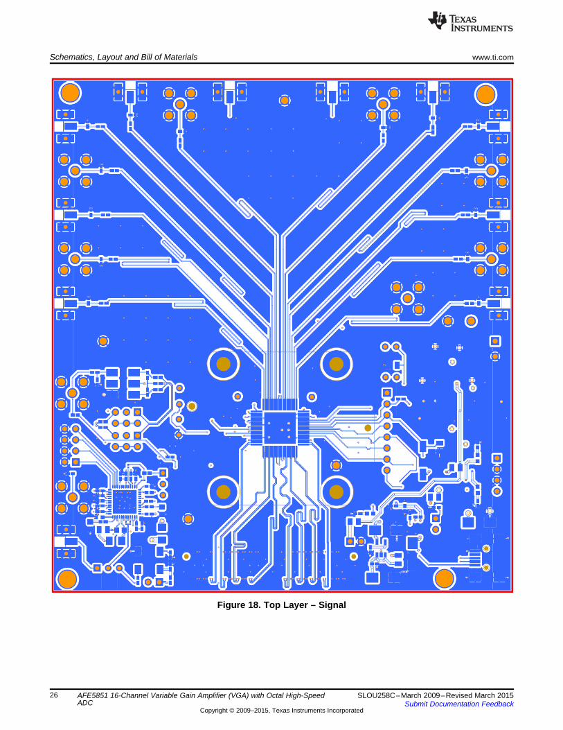
Figure 18. Top Layer – Signal
26 AFE5851 16-Channel Variable Gain Amplifier (VGA) with Octal High-Speed SLOU258C–March 2009–Revised March 2015ADC Submit Documentation Feedback
Copyright © 2009–2015, Texas Instruments Incorporated
www.ti.com Schematics, Layout and Bill of Materials
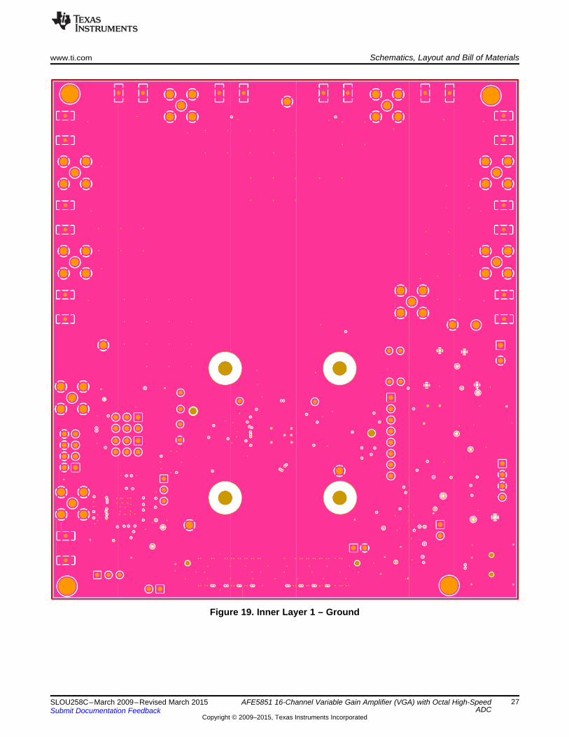
Figure 19. Inner Layer 1 – Ground
27SLOU258C–March 2009–Revised March 2015 AFE5851 16-Channel Variable Gain Amplifier (VGA) with Octal High-SpeedADCSubmit Documentation Feedback
Copyright © 2009–2015, Texas Instruments Incorporated

Schematics, Layout and Bill of Materials www.ti.com
Figure 20. Inner Layer 2 – Signal
28 AFE5851 16-Channel Variable Gain Amplifier (VGA) with Octal High-Speed SLOU258C–March 2009–Revised March 2015ADC Submit Documentation Feedback
Copyright © 2009–2015, Texas Instruments Incorporated
www.ti.com Schematics, Layout and Bill of Materials
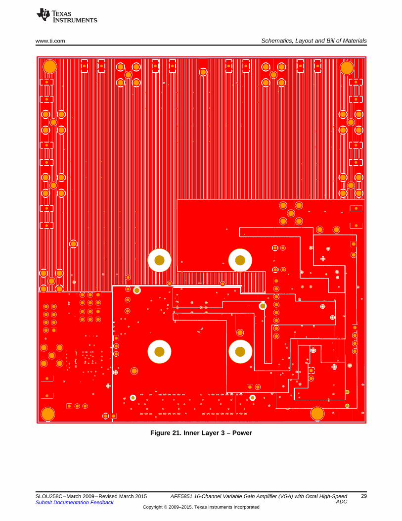
Figure 21. Inner Layer 3 – Power
29SLOU258C–March 2009–Revised March 2015 AFE5851 16-Channel Variable Gain Amplifier (VGA) with Octal High-SpeedADCSubmit Documentation Feedback
Copyright © 2009–2015, Texas Instruments Incorporated

Schematics, Layout and Bill of Materials www.ti.com
Figure 22. Inner Layer 4 – Ground
30 AFE5851 16-Channel Variable Gain Amplifier (VGA) with Octal High-Speed SLOU258C–March 2009–Revised March 2015ADC Submit Documentation Feedback
Copyright © 2009–2015, Texas Instruments Incorporated
www.ti.com Schematics, Layout and Bill of Materials
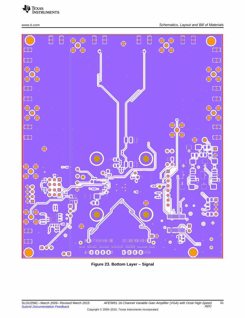
Figure 23. Bottom Layer – Signal
31SLOU258C–March 2009–Revised March 2015 AFE5851 16-Channel Variable Gain Amplifier (VGA) with Octal High-SpeedADCSubmit Documentation Feedback
Copyright © 2009–2015, Texas Instruments Incorporated
Schematics, Layout and Bill of Materials www.ti.com
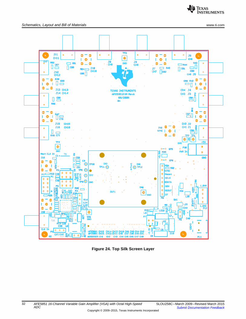
Figure 24. Top Silk Screen Layer
32 AFE5851 16-Channel Variable Gain Amplifier (VGA) with Octal High-Speed SLOU258C–March 2009–Revised March 2015ADC Submit Documentation Feedback
Copyright © 2009–2015, Texas Instruments Incorporated
www.ti.com Schematics, Layout and Bill of Materials
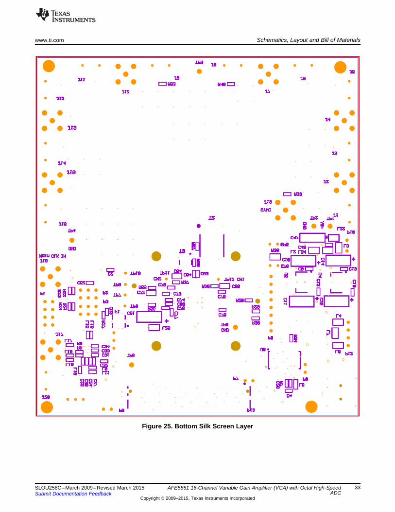
Figure 25. Bottom Silk Screen Layer
33SLOU258C–March 2009–Revised March 2015 AFE5851 16-Channel Variable Gain Amplifier (VGA) with Octal High-SpeedADCSubmit Documentation Feedback
Copyright © 2009–2015, Texas Instruments Incorporated
Schematics, Layout and Bill of Materials www.ti.com
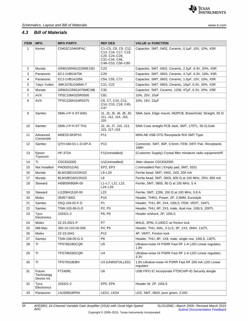
4.3 Bill of Materials
ITEM MFG MFG PART# REF DES VALUE or FUNCTION1 Kemet C0402C104K8PAC C1–C5, C8, C9, C12, Capacitor, SMT, 0402, Ceramic, 0.1μF, 10V, 10%, X5R
C13, C16, C17, C19,C20, C24–C28,C31–C44, C46,C48–C53, C56–C80
2 Murata GRM155R60J225ME15D C23 Capacitor, SMT, 0402, Ceramic, 2.2μF, 6.3V, 20%, X5R3 Panasonic ECJ-1VB0J475K C29 Capacitor, SMT, 0603, Ceramic, 4.7μF, 6.3V, 10%, X5R4 Panasonic ECJ-1VB1A105K C54, C55, C72 Capacitor, SMT, 0603, Ceramic, 1.0μF, 10V, 10%, X5R5 Taiyo Yuden JMK107BJ106MA-T C21, C22 Capacitor, SMT, 0603, Ceramic, 10μF, 6.3V, 20%, X5R6 Murata GRM31CR60J476ME19B C30 Capacitor, SMT, Ceramic, 1206, 47μF, 6.3V, 20%, X5R7 AVX TPSC106K025R0500 C81 10%, 25V, 10uF8 AVX TPSC226K016R0375 C6, C7, C10, C11, 10%, 16V, 22μF
C14, C15, C18, C45,C47
9 Samtec SMA-J-P-X-ST-EM1 J1, J3, J5, J6, J8, J9, SMA Jack, Edge mount, 062PCB, Brass/Gold, Straight, 50 ΩJ11, J12, J14, J16,J20
10 Samtec SMA-J-P-H-ST-TH1 J2, J4, J7, J10, J13, SMA Coax straight PCB Jack, SMT, 175TL, 50 Ω,GoldJ15, J17–J19
11 Advanced MNE20-5K5P10 P11 MINI-AB USB OTG Receptacle R/A SMT TypeConnectek
12 Samtec QTH-040-01-L-D-DP-A P13 Connector, SMT, 80P, 0,5mm, FEM, DIFF Pair, Receptacle,168H
13 Epson HF-372A F1(Uninstalled) (Customer Supply) Crystal filter miniature radio equipment/IFToyocom
14 TI CDCE62005 U1(Uninstalled) Jitter cleaner CDCE6200515 Not Installed PAD0201(UN) EP2, EP3 ( Uninstalled Part ) Empty pad, SMT, 020116 Murata BLM15BD102SN1D L9–L20 Ferrite bead, SMT, 0402, 1kΩ, 200 mA17 Murata BLM18EG601SN1D L8 Ferrite bead, SMT, 0603, 600 Ω at 100 MHz, 25%, 800 mA18 Steward HI0805R800R-00 L1–L7, L21, L22, Ferrite, SMT, 0805, 80 Ω at 100 MHz, 5 A
L24–L2619 Steward LI1206H151R-00 L23 Ferrite, SMT, 1206, 150 Ω at 100 MHz, 0.8 A20 Molex 39357-0002 P10 Header, THRU, Power, 2P, 3.5MM, Eurostyle21 Samtec SSQ-104-02-F-D P1 Header, THU, 8P, 2X4, 100LS, FEM, VERT, 194TL22 Samtec TSW-103-08-G-D P2, P3 Header, THU, 6P, 2X3, male, dual row, 100LS, 200TL23 Tyco 103321-2 P6, P9 Header w/shunt, 2P, 100LS
Electronics24 Molex 22-23-2021-P P7 MALE, 2PIN, 0.100CC w/ friction lock25 Mill-Max 350-10-103-00-006 P4, P5 Header, THU, MAL, 0.1LS, 3P, 1X3, 284H, 110TL26 Molex 22-23-2041 P12 4P, VERT, Friction lock27 Samtec TSW-108-05-G-S P8 Header, THU, 8P, 1X8, male, single row, 100LS, 130TL28 TI TPS79618DCQR U5 Ultralow-noise HI PSRR Fast RF 1-A LDO Linear regulator,
1.8V29 TI TPS79633DCQR U4 Ultralow-noise HI PSRR Fast RF 1-A LDO Linear regulator,
3.3V30 TI TPS79318DBV U3 (UNINSTALLED) 1.8V,Ultralow-noise HI PSRR Fast RF 200 mA LDO Linear
regulator31 Future FT245RL U6 USB FIFO IC Incorporate FTDICHIP-ID Security dongle
TechnologyDevice Int.
32 Tyco 103321-2 EP5, EP6 Header W, 2P, 100LSElectronics
33 Panasonic LNJ308G8PRA LED1, LED4 LED, SMT, 0603, pure green, 2.03V
34 AFE5851 16-Channel Variable Gain Amplifier (VGA) with Octal High-Speed SLOU258C–March 2009–Revised March 2015ADC Submit Documentation Feedback
Copyright © 2009–2015, Texas Instruments Incorporated
www.ti.com Schematics, Layout and Bill of Materials
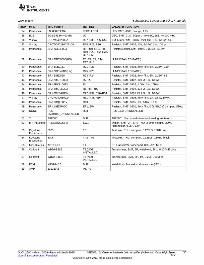
ITEM MFG MFG PART# REF DES VALUE or FUNCTION34 Panasonic LNJ808R8ERA LED2, LED3 LED, SMT, 0603, orange, 1.8V35 ECS ECS-3953M-400-BN U2 OSC, SMT, 3.3V, 50ppm, -40~85C, 5nS, 40.000 MHz36 Vishay CRCW0402000Z R37, R38, R55, R56 0 Ω Jumper,SMT, 0402, thick film, 0 Ω, 1/16W, 5%37 Vishay CRCW04021002F100 R28, R29, R30 Resistor, SMT, 0402, 10K, 1/16W, 1%, 100ppm38 Panasonic ERJ-2GE0R00X R8, R10–R12, R15, Resistor/jumper,SMT, 0402, 0 Ω, 5%, 1/16W
R19, R20, R32, R34,R57, R58
39 Panasonic ERJ-2GEJ0000(UN) R5, R7, R9, R14, ( UNINSTALLED PART )R17, R18
40 Panasonic ERJ-2GEJ131 R21, R22 Resistor, SMT, 0402, thick film, 5%, 1/16W, 13041 Panasonic ERJ-2GEJ49R9(UN) R25, R26 ( UNINSTALLED PART )42 Panasonic ERJ-2GEJ820 R23, R24 Resistor, SMT, 0402, thick film, 5%, 1/16W, 8243 Panasonic ERJ-2RKF1000X R2, R3 Resistor, SMT, 0402, 100 Ω, 1%, 1/16W44 Panasonic ERJ-2RKF1001X R4 Resistor, SMT, 0402, 1.00K, 1%, 1/16W45 Panasonic ERJ-2RKF3320X R1, R6, R16 Resistor, SMT, 0402, 332 Ω, 1%, 1/16W46 Panasonic ERJ-2RKF49R9X R27, R39, R40–R54 Resistor, SMT, 0805 49.9 Ω, 1%, 1/16W47 Vishay CRCW08051002F R31, R35, R36 Resistor, SMT, 0805, thick film, 1%, 1/8W, 10.0K48 Panasonic ERJ-6RQF5R1V R13 Resistor, SMT, 0805, 1%, 1/8W, 5.1 Ω49 Panasonic ERJ-1GE0R00C EP1, EP4 Resistor, SMT, 0201, thick film, 0 Ω, 5%,0 Ω Jumper, 1/20W50 NONE RES- R33 RES 0402 UNINSTALLED
SMT0402_UNINSTALLED51 TI AFE5851 DUT1 AFE5851 16-channel ultrasound analog front-end52 ITT Industries PTS635SK25SM SW1 Switch, SMT, 2P, SPST-NO, 2.5mm Height, MOM,
rectangular, 0.05A, 12V53 Keystone 5005 TP1 Testpoint, THU, compact, 0.125LS, 130TL, red
Electronics54 Keystone 5006 TP2–TP6 Testpoint, THU, compact, 0.125LS, 130TL, black
Electronics55 Mini-Circuits ADTT1-6T T1 RF Transformer wideband, 0.03–125 MHz56 Coilcraft WB36-1SLB T2 (NOT Transformer, SMT, 6P, wideband, 36:1, 0.100–45MHz
INSTALLED)57 Coilcraft WBC4-1TLB T3 (NOT Transformer, SMT, 6P, 1:4, 0.250~750MHz
INSTALLED)58 PEM KFS2-M2.5 DUT1 Install first ( Manually calculate the QTY )59 AMP 531220-2 P6, P9
35SLOU258C–March 2009–Revised March 2015 AFE5851 16-Channel Variable Gain Amplifier (VGA) with Octal High-SpeedADCSubmit Documentation Feedback
Copyright © 2009–2015, Texas Instruments Incorporated
Schematics, Layout and Bill of Materials www.ti.com
36 AFE5851 16-Channel Variable Gain Amplifier (VGA) with Octal High-Speed SLOU258C–March 2009–Revised March 2015ADC Submit Documentation Feedback
Copyright © 2009–2015, Texas Instruments Incorporated
www.ti.com Typical Performance
5 Typical PerformanceThis chapter provides some typical performance of the AFE5851EVM to assist users to verify their setup.
A typical performance plot of the AFE5851 is shown in Figure 26 with 30dB digital gain setting in the 8-CHmode.
37SLOU258C–March 2009–Revised March 2015 AFE5851 16-Channel Variable Gain Amplifier (VGA) with Octal High-SpeedADCSubmit Documentation Feedback
Copyright © 2009–2015, Texas Instruments Incorporated
Typical Performance www.ti.com
Figure 26. Typical Performance of AFE5851 — (a) Fixed Gain Mode; (b) Variable Gain Mode
38 AFE5851 16-Channel Variable Gain Amplifier (VGA) with Octal High-Speed SLOU258C–March 2009–Revised March 2015ADC Submit Documentation Feedback
Copyright © 2009–2015, Texas Instruments Incorporated
Appendix ASLOU258C–March 2009–Revised March 2015
TSW1400 for Evaluating AFE5851
A.1 IntroductionThis application note goes through the steps of evaluating the AFE5851 using the TSW1400EVM.
Step 1: Hardware Setup
Figure 27. Connection Between TSW1400EVM and AFE5851
39SLOU258C–March 2009–Revised March 2015 TSW1400 for Evaluating AFE5851Submit Documentation Feedback
Copyright © 2009–2015, Texas Instruments Incorporated

Introduction www.ti.com
Figure 28. Connecting the Instruments
40 TSW1400 for Evaluating AFE5851 SLOU258C–March 2009–Revised March 2015Submit Documentation Feedback
Copyright © 2009–2015, Texas Instruments Incorporated

www.ti.com Introduction
Step 2: Launch AFE5851 GUIFrom PC click Start Menu → All Programs → Texas Instruments → AFE58X1EVM USB SPI →AFE58X1EVM USB SPI
The GUI may be running if the following screen appears.
Figure 29. AFE5851 EVM GUI –Run Mode
41SLOU258C–March 2009–Revised March 2015 TSW1400 for Evaluating AFE5851Submit Documentation Feedback
Copyright © 2009–2015, Texas Instruments Incorporated
Introduction www.ti.com
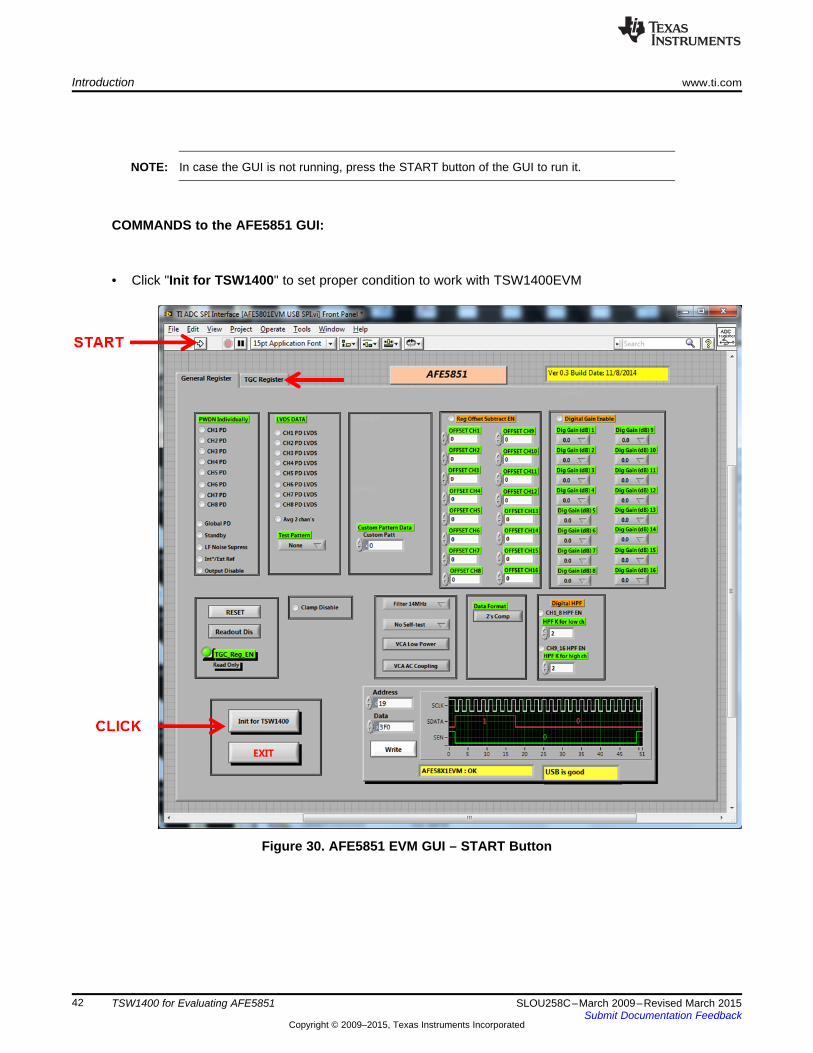
NOTE: In case the GUI is not running, press the START button of the GUI to run it.
COMMANDS to the AFE5851 GUI:
• Click "Init for TSW1400" to set proper condition to work with TSW1400EVM
Figure 30. AFE5851 EVM GUI – START Button
42 TSW1400 for Evaluating AFE5851 SLOU258C–March 2009–Revised March 2015Submit Documentation Feedback
Copyright © 2009–2015, Texas Instruments Incorporated
www.ti.com Introduction
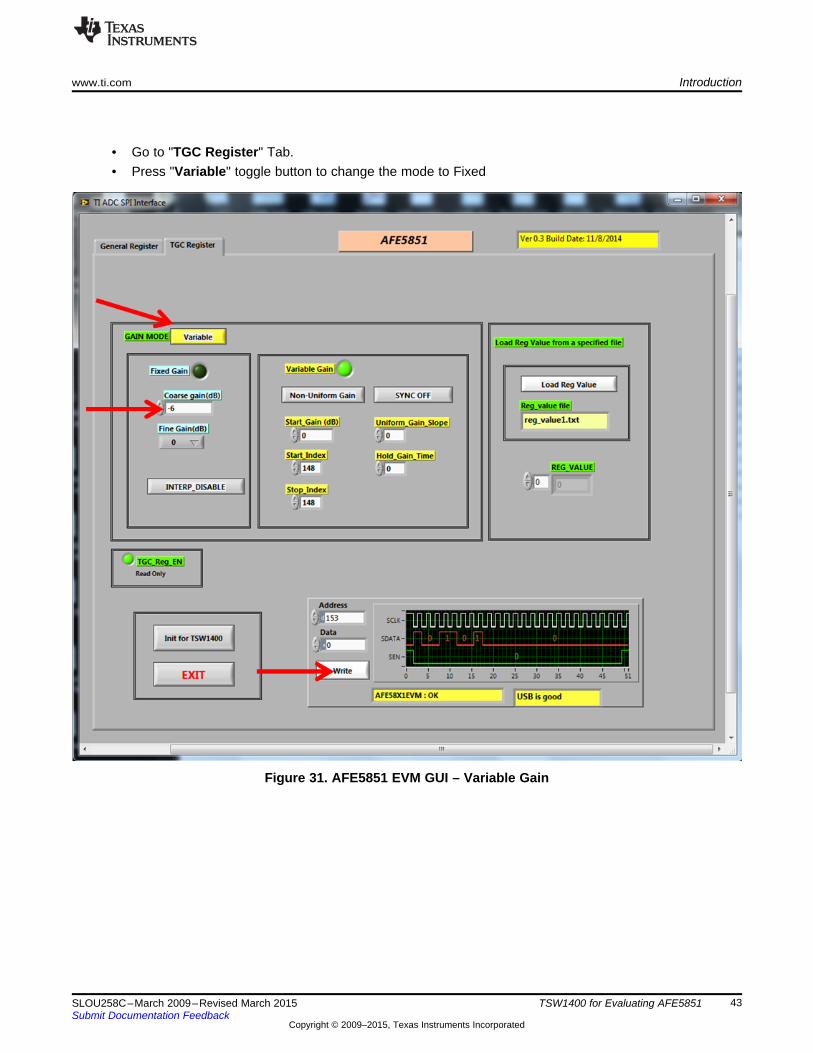
• Go to "TGC Register" Tab.• Press "Variable" toggle button to change the mode to Fixed
Figure 31. AFE5851 EVM GUI – Variable Gain
43SLOU258C–March 2009–Revised March 2015 TSW1400 for Evaluating AFE5851Submit Documentation Feedback
Copyright © 2009–2015, Texas Instruments Incorporated

Introduction www.ti.com
• Type 30 and press "Write" button
Figure 32. AFE5851 EVM GUI – Setting Fixed Gain
• At this stage the AFE5851 is ready.
44 TSW1400 for Evaluating AFE5851 SLOU258C–March 2009–Revised March 2015Submit Documentation Feedback
Copyright © 2009–2015, Texas Instruments Incorporated
www.ti.com Introduction
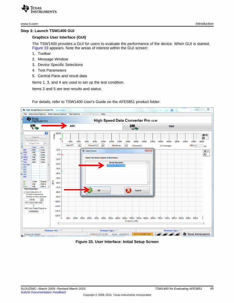
Step 3: Launch TSW1400 GUIGraphics User Interface (GUI)The TSW1400 provides a GUI for users to evaluate the performance of the device. When GUI is started,Figure 33 appears. Note the areas of interest within the GUI screen:1. Toolbar2. Message Window3. Device Specific Selections4. Test Parameters5. Central Pane and result data
Items 1, 3, and 4 are used to set up the test condition.
Items 2 and 5 are test results and status.
For details, refer to TSW1400 User's Guide on the AFE5851 product folder.
Figure 33. User Interface: Initial Setup Screen
45SLOU258C–March 2009–Revised March 2015 TSW1400 for Evaluating AFE5851Submit Documentation Feedback
Copyright © 2009–2015, Texas Instruments Incorporated
Introduction www.ti.com
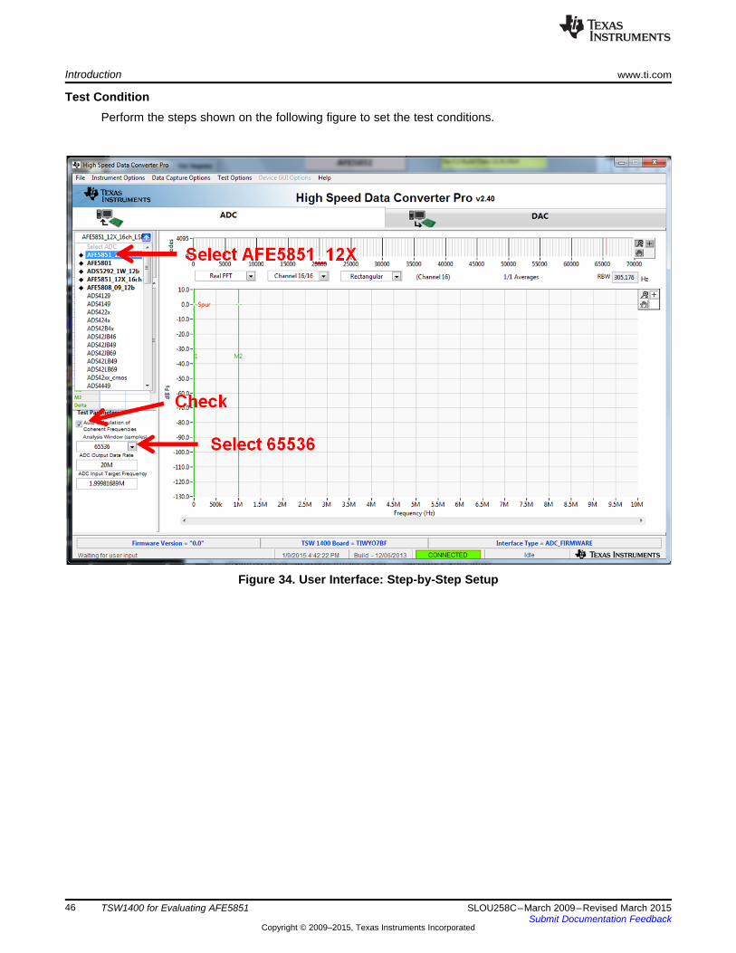
Test ConditionPerform the steps shown on the following figure to set the test conditions.
Figure 34. User Interface: Step-by-Step Setup
46 TSW1400 for Evaluating AFE5851 SLOU258C–March 2009–Revised March 2015Submit Documentation Feedback
Copyright © 2009–2015, Texas Instruments Incorporated
www.ti.com Introduction
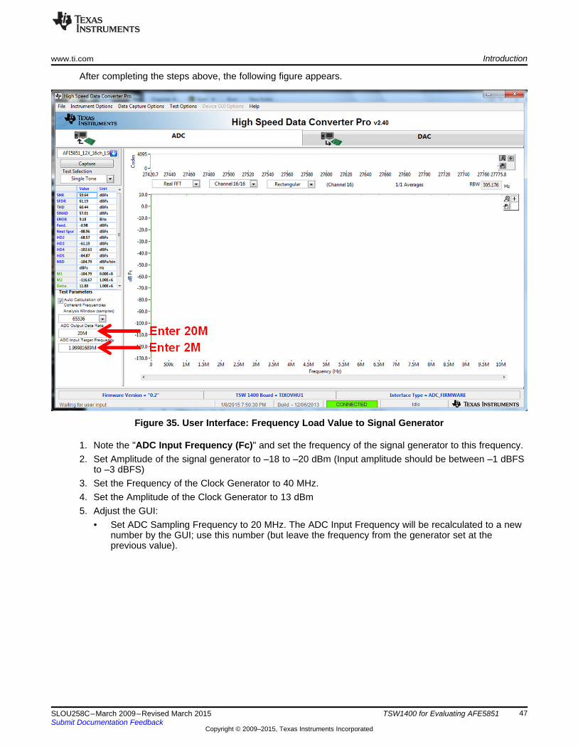
After completing the steps above, the following figure appears.
Figure 35. User Interface: Frequency Load Value to Signal Generator
1. Note the "ADC Input Frequency (Fc)" and set the frequency of the signal generator to this frequency.2. Set Amplitude of the signal generator to –18 to –20 dBm (Input amplitude should be between –1 dBFS
to –3 dBFS)3. Set the Frequency of the Clock Generator to 40 MHz.4. Set the Amplitude of the Clock Generator to 13 dBm5. Adjust the GUI:
• Set ADC Sampling Frequency to 20 MHz. The ADC Input Frequency will be recalculated to a newnumber by the GUI; use this number (but leave the frequency from the generator set at theprevious value).
47SLOU258C–March 2009–Revised March 2015 TSW1400 for Evaluating AFE5851Submit Documentation Feedback
Copyright © 2009–2015, Texas Instruments Incorporated
Introduction www.ti.com
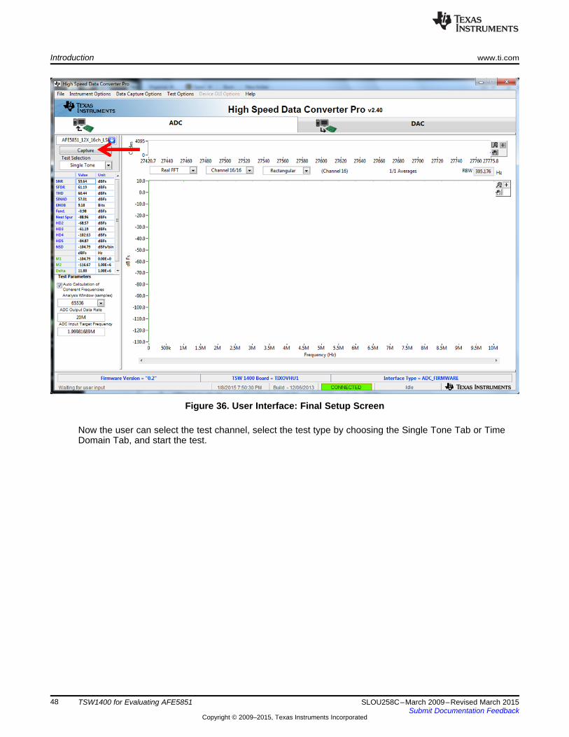
Figure 36. User Interface: Final Setup Screen
Now the user can select the test channel, select the test type by choosing the Single Tone Tab or TimeDomain Tab, and start the test.
48 TSW1400 for Evaluating AFE5851 SLOU258C–March 2009–Revised March 2015Submit Documentation Feedback
Copyright © 2009–2015, Texas Instruments Incorporated

www.ti.com Introduction
Single Tone FFTThe Single Tone FFT test is shown in Figure 37. The larger central pane displays the FFT powerspectrum, whereas the calculated statistics are grouped into categories on the right of the screen. Settingsand inputs relevant to the test are entered in drop-down menus or text input boxes on the left portion ofthe window.
Figure 37. User Interface: Single FFT Format
49SLOU258C–March 2009–Revised March 2015 TSW1400 for Evaluating AFE5851Submit Documentation Feedback
Copyright © 2009–2015, Texas Instruments Incorporated

Introduction www.ti.com
Time DomainThe Time Domain test is shown in Figure 38. The larger central pane displays the raw sampled datawhereas the calculated statistics are grouped into categories on the right of the screen. Settings andinputs relevant to the test are entered in drop-down menus or text input boxes on the left portion of thewindow.
Figure 38. User Interface: Time Domain Format
50 TSW1400 for Evaluating AFE5851 SLOU258C–March 2009–Revised March 2015Submit Documentation Feedback
Copyright © 2009–2015, Texas Instruments Incorporated
www.ti.com Introduction
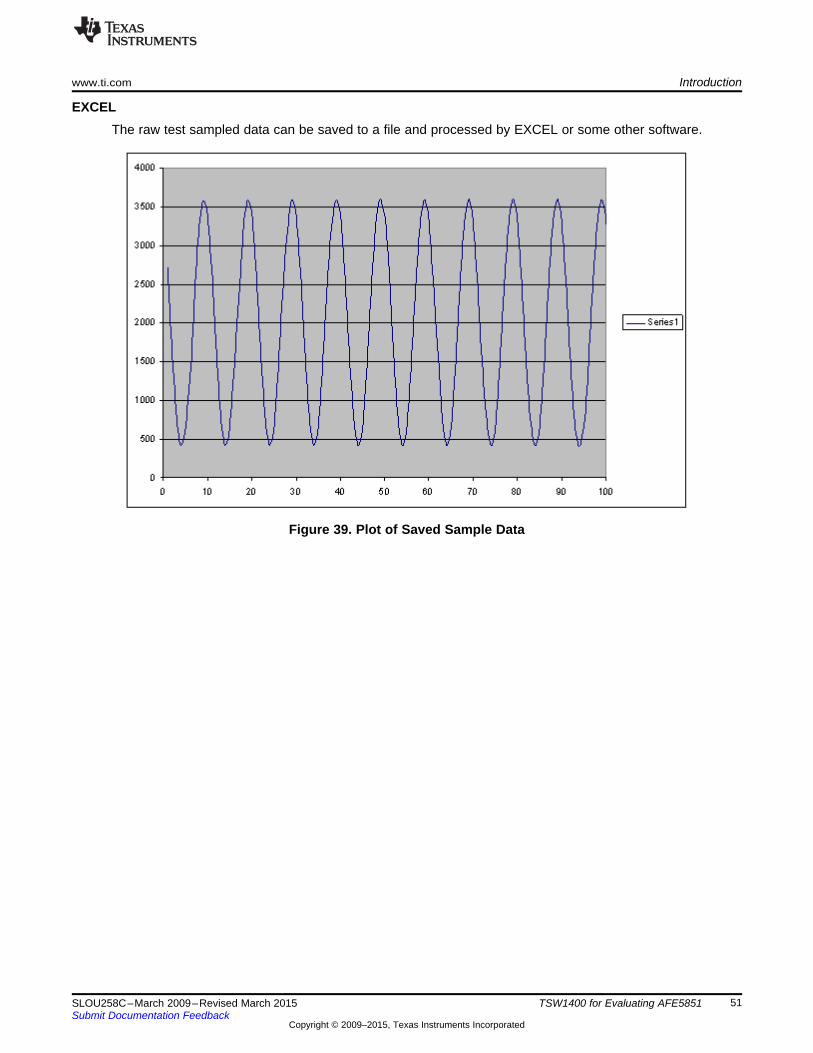
EXCELThe raw test sampled data can be saved to a file and processed by EXCEL or some other software.
Figure 39. Plot of Saved Sample Data
51SLOU258C–March 2009–Revised March 2015 TSW1400 for Evaluating AFE5851Submit Documentation Feedback
Copyright © 2009–2015, Texas Instruments Incorporated
Appendix BSLOU258C–March 2009–Revised March 2015
High Speed Data Converter Pro (HSDCPro) GUIInstallation
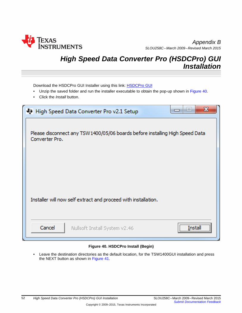
Download the HSDCPro GUI Installer using this link: HSDCPro GUI• Unzip the saved folder and run the installer executable to obtain the pop-up shown in Figure 40.• Click the Install button.
Figure 40. HSDCPro Install (Begin)
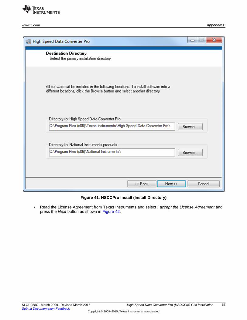
• Leave the destination directories as the default location, for the TSW1400GUI installation and pressthe NEXT button as shown in Figure 41.
52 High Speed Data Converter Pro (HSDCPro) GUI Installation SLOU258C–March 2009–Revised March 2015Submit Documentation Feedback
Copyright © 2009–2015, Texas Instruments Incorporated
www.ti.com Appendix B
Figure 41. HSDCPro Install (Install Directory)
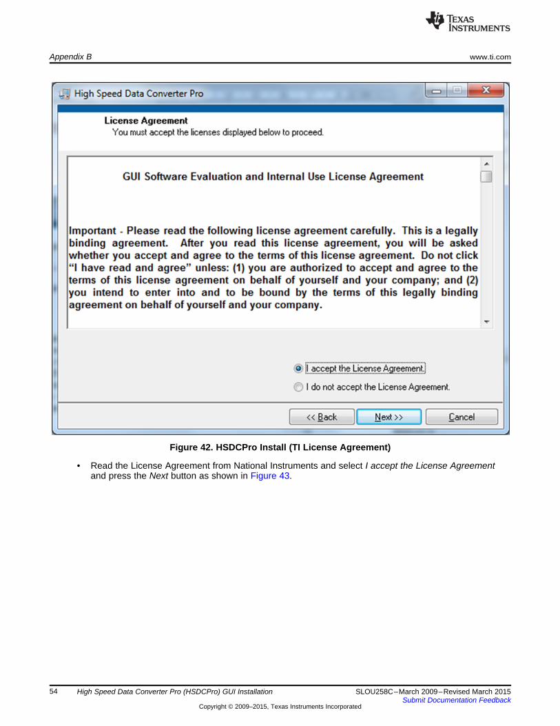
• Read the License Agreement from Texas Instruments and select I accept the License Agreement andpress the Next button as shown in Figure 42.
53SLOU258C–March 2009–Revised March 2015 High Speed Data Converter Pro (HSDCPro) GUI InstallationSubmit Documentation Feedback
Copyright © 2009–2015, Texas Instruments Incorporated
Appendix B www.ti.com
Figure 42. HSDCPro Install (TI License Agreement)
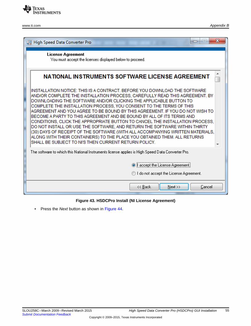
• Read the License Agreement from National Instruments and select I accept the License Agreementand press the Next button as shown in Figure 43.
54 High Speed Data Converter Pro (HSDCPro) GUI Installation SLOU258C–March 2009–Revised March 2015Submit Documentation Feedback
Copyright © 2009–2015, Texas Instruments Incorporated
www.ti.com Appendix B
Figure 43. HSDCPro Install (NI License Agreement)
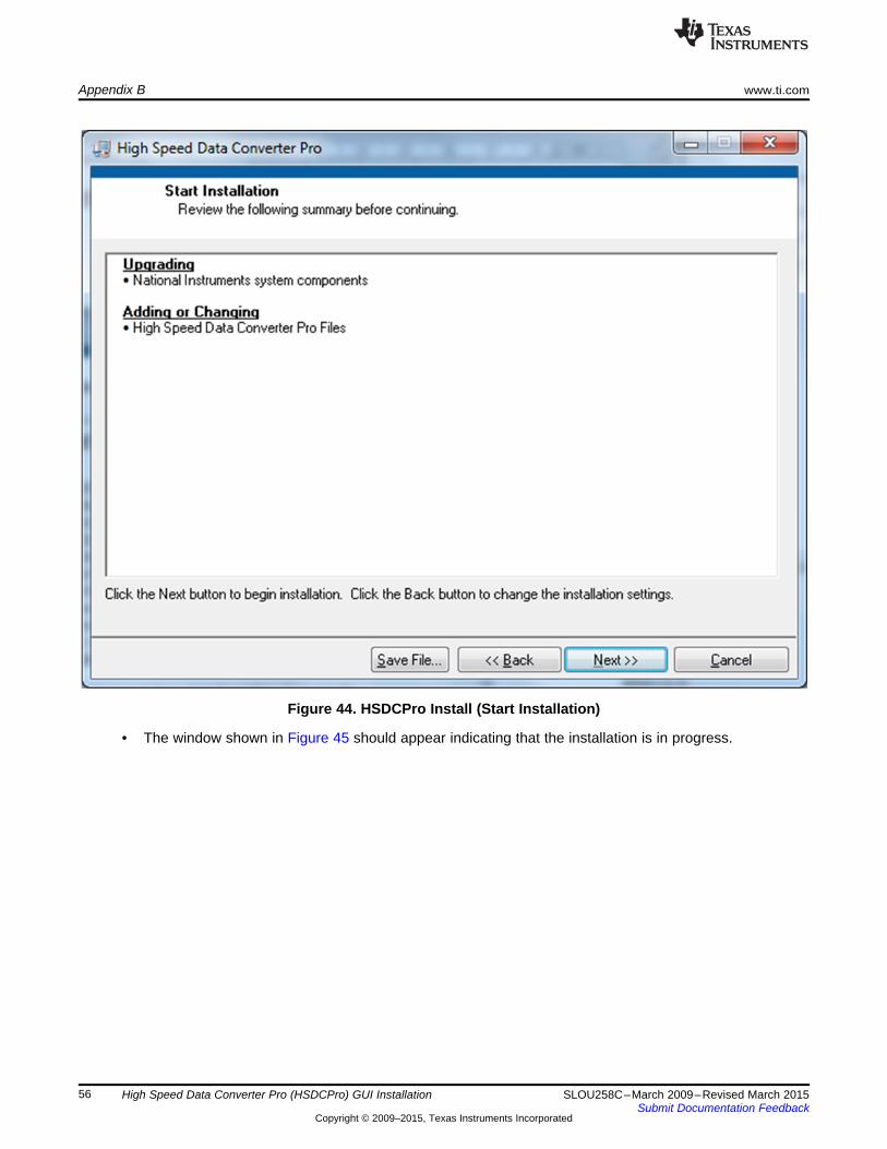
• Press the Next button as shown in Figure 44.
55SLOU258C–March 2009–Revised March 2015 High Speed Data Converter Pro (HSDCPro) GUI InstallationSubmit Documentation Feedback
Copyright © 2009–2015, Texas Instruments Incorporated
Appendix B www.ti.com
Figure 44. HSDCPro Install (Start Installation)
• The window shown in Figure 45 should appear indicating that the installation is in progress.
56 High Speed Data Converter Pro (HSDCPro) GUI Installation SLOU258C–March 2009–Revised March 2015Submit Documentation Feedback
Copyright © 2009–2015, Texas Instruments Incorporated

www.ti.com Appendix B
Figure 45. HSDCPro Install (Installation Progress)
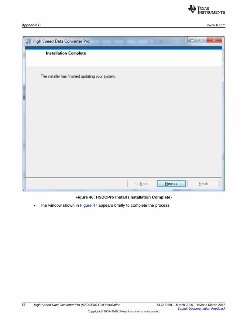
• The window shown in Figure 46 appears indicating Installation Complete. Press the Next button.
57SLOU258C–March 2009–Revised March 2015 High Speed Data Converter Pro (HSDCPro) GUI InstallationSubmit Documentation Feedback
Copyright © 2009–2015, Texas Instruments Incorporated
Appendix B www.ti.com
Figure 46. HSDCPro Install (Installation Complete)
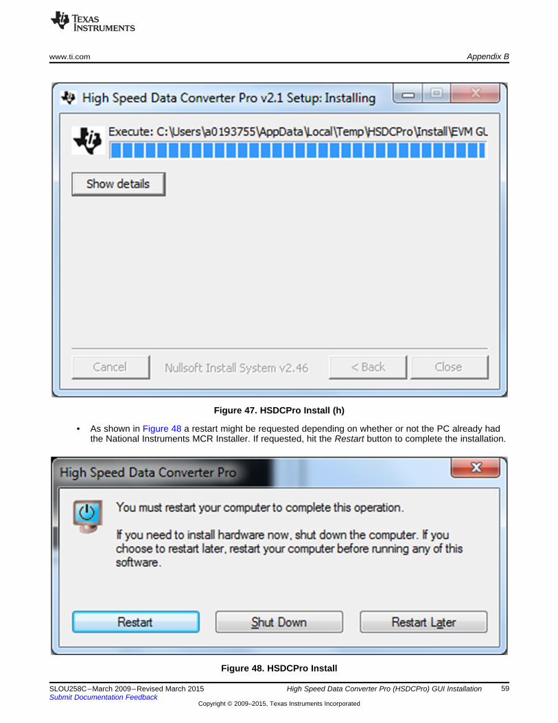
• The window shown in Figure 47 appears briefly to complete the process.
58 High Speed Data Converter Pro (HSDCPro) GUI Installation SLOU258C–March 2009–Revised March 2015Submit Documentation Feedback
Copyright © 2009–2015, Texas Instruments Incorporated
www.ti.com Appendix B
Figure 47. HSDCPro Install (h)
• As shown in Figure 48 a restart might be requested depending on whether or not the PC already hadthe National Instruments MCR Installer. If requested, hit the Restart button to complete the installation.
Figure 48. HSDCPro Install
59SLOU258C–March 2009–Revised March 2015 High Speed Data Converter Pro (HSDCPro) GUI InstallationSubmit Documentation Feedback
Copyright © 2009–2015, Texas Instruments Incorporated
STANDARD TERMS AND CONDITIONS FOR EVALUATION MODULES1. Delivery: TI delivers TI evaluation boards, kits, or modules, including any accompanying demonstration software, components, or
documentation (collectively, an “EVM” or “EVMs”) to the User (“User”) in accordance with the terms and conditions set forth herein.Acceptance of the EVM is expressly subject to the following terms and conditions.1.1 EVMs are intended solely for product or software developers for use in a research and development setting to facilitate feasibility
evaluation, experimentation, or scientific analysis of TI semiconductors products. EVMs have no direct function and are notfinished products. EVMs shall not be directly or indirectly assembled as a part or subassembly in any finished product. Forclarification, any software or software tools provided with the EVM (“Software”) shall not be subject to the terms and conditionsset forth herein but rather shall be subject to the applicable terms and conditions that accompany such Software
1.2 EVMs are not intended for consumer or household use. EVMs may not be sold, sublicensed, leased, rented, loaned, assigned,or otherwise distributed for commercial purposes by Users, in whole or in part, or used in any finished product or productionsystem.
2 Limited Warranty and Related Remedies/Disclaimers:2.1 These terms and conditions do not apply to Software. The warranty, if any, for Software is covered in the applicable Software
License Agreement.2.2 TI warrants that the TI EVM will conform to TI's published specifications for ninety (90) days after the date TI delivers such EVM
to User. Notwithstanding the foregoing, TI shall not be liable for any defects that are caused by neglect, misuse or mistreatmentby an entity other than TI, including improper installation or testing, or for any EVMs that have been altered or modified in anyway by an entity other than TI. Moreover, TI shall not be liable for any defects that result from User's design, specifications orinstructions for such EVMs. Testing and other quality control techniques are used to the extent TI deems necessary or asmandated by government requirements. TI does not test all parameters of each EVM.
2.3 If any EVM fails to conform to the warranty set forth above, TI's sole liability shall be at its option to repair or replace such EVM,or credit User's account for such EVM. TI's liability under this warranty shall be limited to EVMs that are returned during thewarranty period to the address designated by TI and that are determined by TI not to conform to such warranty. If TI elects torepair or replace such EVM, TI shall have a reasonable time to repair such EVM or provide replacements. Repaired EVMs shallbe warranted for the remainder of the original warranty period. Replaced EVMs shall be warranted for a new full ninety (90) daywarranty period.
3 Regulatory Notices:3.1 United States
3.1.1 Notice applicable to EVMs not FCC-Approved:This kit is designed to allow product developers to evaluate electronic components, circuitry, or software associated with the kitto determine whether to incorporate such items in a finished product and software developers to write software applications foruse with the end product. This kit is not a finished product and when assembled may not be resold or otherwise marketed unlessall required FCC equipment authorizations are first obtained. Operation is subject to the condition that this product not causeharmful interference to licensed radio stations and that this product accept harmful interference. Unless the assembled kit isdesigned to operate under part 15, part 18 or part 95 of this chapter, the operator of the kit must operate under the authority ofan FCC license holder or must secure an experimental authorization under part 5 of this chapter.3.1.2 For EVMs annotated as FCC – FEDERAL COMMUNICATIONS COMMISSION Part 15 Compliant:
CAUTIONThis device complies with part 15 of the FCC Rules. Operation is subject to the following two conditions: (1) This device may notcause harmful interference, and (2) this device must accept any interference received, including interference that may causeundesired operation.Changes or modifications not expressly approved by the party responsible for compliance could void the user's authority tooperate the equipment.
FCC Interference Statement for Class A EVM devicesNOTE: This equipment has been tested and found to comply with the limits for a Class A digital device, pursuant to part 15 ofthe FCC Rules. These limits are designed to provide reasonable protection against harmful interference when the equipment isoperated in a commercial environment. This equipment generates, uses, and can radiate radio frequency energy and, if notinstalled and used in accordance with the instruction manual, may cause harmful interference to radio communications.Operation of this equipment in a residential area is likely to cause harmful interference in which case the user will be required tocorrect the interference at his own expense.
SPACER
SPACER
SPACER
SPACER
SPACER
SPACER
SPACER
SPACER
FCC Interference Statement for Class B EVM devicesNOTE: This equipment has been tested and found to comply with the limits for a Class B digital device, pursuant to part 15 ofthe FCC Rules. These limits are designed to provide reasonable protection against harmful interference in a residentialinstallation. This equipment generates, uses and can radiate radio frequency energy and, if not installed and used in accordancewith the instructions, may cause harmful interference to radio communications. However, there is no guarantee that interferencewill not occur in a particular installation. If this equipment does cause harmful interference to radio or television reception, whichcan be determined by turning the equipment off and on, the user is encouraged to try to correct the interference by one or moreof the following measures:
• Reorient or relocate the receiving antenna.• Increase the separation between the equipment and receiver.• Connect the equipment into an outlet on a circuit different from that to which the receiver is connected.• Consult the dealer or an experienced radio/TV technician for help.
3.2 Canada3.2.1 For EVMs issued with an Industry Canada Certificate of Conformance to RSS-210
Concerning EVMs Including Radio Transmitters:This device complies with Industry Canada license-exempt RSS standard(s). Operation is subject to the following two conditions:(1) this device may not cause interference, and (2) this device must accept any interference, including interference that maycause undesired operation of the device.
Concernant les EVMs avec appareils radio:Le présent appareil est conforme aux CNR d'Industrie Canada applicables aux appareils radio exempts de licence. L'exploitationest autorisée aux deux conditions suivantes: (1) l'appareil ne doit pas produire de brouillage, et (2) l'utilisateur de l'appareil doitaccepter tout brouillage radioélectrique subi, même si le brouillage est susceptible d'en compromettre le fonctionnement.
Concerning EVMs Including Detachable Antennas:Under Industry Canada regulations, this radio transmitter may only operate using an antenna of a type and maximum (or lesser)gain approved for the transmitter by Industry Canada. To reduce potential radio interference to other users, the antenna typeand its gain should be so chosen that the equivalent isotropically radiated power (e.i.r.p.) is not more than that necessary forsuccessful communication. This radio transmitter has been approved by Industry Canada to operate with the antenna typeslisted in the user guide with the maximum permissible gain and required antenna impedance for each antenna type indicated.Antenna types not included in this list, having a gain greater than the maximum gain indicated for that type, are strictly prohibitedfor use with this device.
Concernant les EVMs avec antennes détachablesConformément à la réglementation d'Industrie Canada, le présent émetteur radio peut fonctionner avec une antenne d'un type etd'un gain maximal (ou inférieur) approuvé pour l'émetteur par Industrie Canada. Dans le but de réduire les risques de brouillageradioélectrique à l'intention des autres utilisateurs, il faut choisir le type d'antenne et son gain de sorte que la puissance isotroperayonnée équivalente (p.i.r.e.) ne dépasse pas l'intensité nécessaire à l'établissement d'une communication satisfaisante. Leprésent émetteur radio a été approuvé par Industrie Canada pour fonctionner avec les types d'antenne énumérés dans lemanuel d’usage et ayant un gain admissible maximal et l'impédance requise pour chaque type d'antenne. Les types d'antennenon inclus dans cette liste, ou dont le gain est supérieur au gain maximal indiqué, sont strictement interdits pour l'exploitation del'émetteur
3.3 Japan3.3.1 Notice for EVMs delivered in Japan: Please see http://www.tij.co.jp/lsds/ti_ja/general/eStore/notice_01.page 日本国内に
輸入される評価用キット、ボードについては、次のところをご覧ください。http://www.tij.co.jp/lsds/ti_ja/general/eStore/notice_01.page
3.3.2 Notice for Users of EVMs Considered “Radio Frequency Products” in Japan: EVMs entering Japan are NOT certified byTI as conforming to Technical Regulations of Radio Law of Japan.
If User uses EVMs in Japan, User is required by Radio Law of Japan to follow the instructions below with respect to EVMs:1. Use EVMs in a shielded room or any other test facility as defined in the notification #173 issued by Ministry of Internal
Affairs and Communications on March 28, 2006, based on Sub-section 1.1 of Article 6 of the Ministry’s Rule forEnforcement of Radio Law of Japan,
2. Use EVMs only after User obtains the license of Test Radio Station as provided in Radio Law of Japan with respect toEVMs, or
3. Use of EVMs only after User obtains the Technical Regulations Conformity Certification as provided in Radio Law of Japanwith respect to EVMs. Also, do not transfer EVMs, unless User gives the same notice above to the transferee. Please notethat if User does not follow the instructions above, User will be subject to penalties of Radio Law of Japan.
SPACER
SPACER
SPACER
SPACER
SPACER
【無線電波を送信する製品の開発キットをお使いになる際の注意事項】本開発キットは技術基準適合証明を受けておりません。本製品のご使用に際しては、電波法遵守のため、以下のいずれかの措置を取っていただく必要がありますのでご注意ください。1. 電波法施行規則第6条第1項第1号に基づく平成18年3月28日総務省告示第173号で定められた電波暗室等の試験設備でご使用
いただく。2. 実験局の免許を取得後ご使用いただく。3. 技術基準適合証明を取得後ご使用いただく。
なお、本製品は、上記の「ご使用にあたっての注意」を譲渡先、移転先に通知しない限り、譲渡、移転できないものとします。上記を遵守頂けない場合は、電波法の罰則が適用される可能性があることをご留意ください。
日本テキサス・インスツルメンツ株式会社東京都新宿区西新宿6丁目24番1号西新宿三井ビル
3.3.3 Notice for EVMs for Power Line Communication: Please see http://www.tij.co.jp/lsds/ti_ja/general/eStore/notice_02.page電力線搬送波通信についての開発キットをお使いになる際の注意事項については、次のところをご覧ください。http://www.tij.co.jp/lsds/ti_ja/general/eStore/notice_02.page
SPACER4 EVM Use Restrictions and Warnings:
4.1 EVMS ARE NOT FOR USE IN FUNCTIONAL SAFETY AND/OR SAFETY CRITICAL EVALUATIONS, INCLUDING BUT NOTLIMITED TO EVALUATIONS OF LIFE SUPPORT APPLICATIONS.
4.2 User must read and apply the user guide and other available documentation provided by TI regarding the EVM prior to handlingor using the EVM, including without limitation any warning or restriction notices. The notices contain important safety informationrelated to, for example, temperatures and voltages.
4.3 Safety-Related Warnings and Restrictions:4.3.1 User shall operate the EVM within TI’s recommended specifications and environmental considerations stated in the user
guide, other available documentation provided by TI, and any other applicable requirements and employ reasonable andcustomary safeguards. Exceeding the specified performance ratings and specifications (including but not limited to inputand output voltage, current, power, and environmental ranges) for the EVM may cause personal injury or death, orproperty damage. If there are questions concerning performance ratings and specifications, User should contact a TIfield representative prior to connecting interface electronics including input power and intended loads. Any loads appliedoutside of the specified output range may also result in unintended and/or inaccurate operation and/or possiblepermanent damage to the EVM and/or interface electronics. Please consult the EVM user guide prior to connecting anyload to the EVM output. If there is uncertainty as to the load specification, please contact a TI field representative.During normal operation, even with the inputs and outputs kept within the specified allowable ranges, some circuitcomponents may have elevated case temperatures. These components include but are not limited to linear regulators,switching transistors, pass transistors, current sense resistors, and heat sinks, which can be identified using theinformation in the associated documentation. When working with the EVM, please be aware that the EVM may becomevery warm.
4.3.2 EVMs are intended solely for use by technically qualified, professional electronics experts who are familiar with thedangers and application risks associated with handling electrical mechanical components, systems, and subsystems.User assumes all responsibility and liability for proper and safe handling and use of the EVM by User or its employees,affiliates, contractors or designees. User assumes all responsibility and liability to ensure that any interfaces (electronicand/or mechanical) between the EVM and any human body are designed with suitable isolation and means to safelylimit accessible leakage currents to minimize the risk of electrical shock hazard. User assumes all responsibility andliability for any improper or unsafe handling or use of the EVM by User or its employees, affiliates, contractors ordesignees.
4.4 User assumes all responsibility and liability to determine whether the EVM is subject to any applicable international, federal,state, or local laws and regulations related to User’s handling and use of the EVM and, if applicable, User assumes allresponsibility and liability for compliance in all respects with such laws and regulations. User assumes all responsibility andliability for proper disposal and recycling of the EVM consistent with all applicable international, federal, state, and localrequirements.
5. Accuracy of Information: To the extent TI provides information on the availability and function of EVMs, TI attempts to be as accurateas possible. However, TI does not warrant the accuracy of EVM descriptions, EVM availability or other information on its websites asaccurate, complete, reliable, current, or error-free.
SPACER
SPACER
SPACER
SPACER
SPACER
SPACER

SPACER6. Disclaimers:
6.1 EXCEPT AS SET FORTH ABOVE, EVMS AND ANY WRITTEN DESIGN MATERIALS PROVIDED WITH THE EVM (AND THEDESIGN OF THE EVM ITSELF) ARE PROVIDED "AS IS" AND "WITH ALL FAULTS." TI DISCLAIMS ALL OTHERWARRANTIES, EXPRESS OR IMPLIED, REGARDING SUCH ITEMS, INCLUDING BUT NOT LIMITED TO ANY IMPLIEDWARRANTIES OF MERCHANTABILITY OR FITNESS FOR A PARTICULAR PURPOSE OR NON-INFRINGEMENT OF ANYTHIRD PARTY PATENTS, COPYRIGHTS, TRADE SECRETS OR OTHER INTELLECTUAL PROPERTY RIGHTS.
6.2 EXCEPT FOR THE LIMITED RIGHT TO USE THE EVM SET FORTH HEREIN, NOTHING IN THESE TERMS ANDCONDITIONS SHALL BE CONSTRUED AS GRANTING OR CONFERRING ANY RIGHTS BY LICENSE, PATENT, OR ANYOTHER INDUSTRIAL OR INTELLECTUAL PROPERTY RIGHT OF TI, ITS SUPPLIERS/LICENSORS OR ANY OTHER THIRDPARTY, TO USE THE EVM IN ANY FINISHED END-USER OR READY-TO-USE FINAL PRODUCT, OR FOR ANYINVENTION, DISCOVERY OR IMPROVEMENT MADE, CONCEIVED OR ACQUIRED PRIOR TO OR AFTER DELIVERY OFTHE EVM.
7. USER'S INDEMNITY OBLIGATIONS AND REPRESENTATIONS. USER WILL DEFEND, INDEMNIFY AND HOLD TI, ITSLICENSORS AND THEIR REPRESENTATIVES HARMLESS FROM AND AGAINST ANY AND ALL CLAIMS, DAMAGES, LOSSES,EXPENSES, COSTS AND LIABILITIES (COLLECTIVELY, "CLAIMS") ARISING OUT OF OR IN CONNECTION WITH ANYHANDLING OR USE OF THE EVM THAT IS NOT IN ACCORDANCE WITH THESE TERMS AND CONDITIONS. THIS OBLIGATIONSHALL APPLY WHETHER CLAIMS ARISE UNDER STATUTE, REGULATION, OR THE LAW OF TORT, CONTRACT OR ANYOTHER LEGAL THEORY, AND EVEN IF THE EVM FAILS TO PERFORM AS DESCRIBED OR EXPECTED.
8. Limitations on Damages and Liability:8.1 General Limitations. IN NO EVENT SHALL TI BE LIABLE FOR ANY SPECIAL, COLLATERAL, INDIRECT, PUNITIVE,
INCIDENTAL, CONSEQUENTIAL, OR EXEMPLARY DAMAGES IN CONNECTION WITH OR ARISING OUT OF THESETERMS ANDCONDITIONS OR THE USE OF THE EVMS PROVIDED HEREUNDER, REGARDLESS OF WHETHER TI HASBEEN ADVISED OF THE POSSIBILITY OF SUCH DAMAGES. EXCLUDED DAMAGES INCLUDE, BUT ARE NOT LIMITEDTO, COST OF REMOVAL OR REINSTALLATION, ANCILLARY COSTS TO THE PROCUREMENT OF SUBSTITUTE GOODSOR SERVICES, RETESTING, OUTSIDE COMPUTER TIME, LABOR COSTS, LOSS OF GOODWILL, LOSS OF PROFITS,LOSS OF SAVINGS, LOSS OF USE, LOSS OF DATA, OR BUSINESS INTERRUPTION. NO CLAIM, SUIT OR ACTION SHALLBE BROUGHT AGAINST TI MORE THAN ONE YEAR AFTER THE RELATED CAUSE OF ACTION HAS OCCURRED.
8.2 Specific Limitations. IN NO EVENT SHALL TI'S AGGREGATE LIABILITY FROM ANY WARRANTY OR OTHER OBLIGATIONARISING OUT OF OR IN CONNECTION WITH THESE TERMS AND CONDITIONS, OR ANY USE OF ANY TI EVMPROVIDED HEREUNDER, EXCEED THE TOTAL AMOUNT PAID TO TI FOR THE PARTICULAR UNITS SOLD UNDERTHESE TERMS AND CONDITIONS WITH RESPECT TO WHICH LOSSES OR DAMAGES ARE CLAIMED. THE EXISTENCEOF MORE THAN ONE CLAIM AGAINST THE PARTICULAR UNITS SOLD TO USER UNDER THESE TERMS ANDCONDITIONS SHALL NOT ENLARGE OR EXTEND THIS LIMIT.
9. Return Policy. Except as otherwise provided, TI does not offer any refunds, returns, or exchanges. Furthermore, no return of EVM(s)will be accepted if the package has been opened and no return of the EVM(s) will be accepted if they are damaged or otherwise not ina resalable condition. If User feels it has been incorrectly charged for the EVM(s) it ordered or that delivery violates the applicableorder, User should contact TI. All refunds will be made in full within thirty (30) working days from the return of the components(s),excluding any postage or packaging costs.
10. Governing Law: These terms and conditions shall be governed by and interpreted in accordance with the laws of the State of Texas,without reference to conflict-of-laws principles. User agrees that non-exclusive jurisdiction for any dispute arising out of or relating tothese terms and conditions lies within courts located in the State of Texas and consents to venue in Dallas County, Texas.Notwithstanding the foregoing, any judgment may be enforced in any United States or foreign court, and TI may seek injunctive reliefin any United States or foreign court.
Mailing Address: Texas Instruments, Post Office Box 655303, Dallas, Texas 75265Copyright © 2015, Texas Instruments Incorporated
spacer
IMPORTANT NOTICE
Texas Instruments Incorporated and its subsidiaries (TI) reserve the right to make corrections, enhancements, improvements and otherchanges to its semiconductor products and services per JESD46, latest issue, and to discontinue any product or service per JESD48, latestissue. Buyers should obtain the latest relevant information before placing orders and should verify that such information is current andcomplete. All semiconductor products (also referred to herein as “components”) are sold subject to TI’s terms and conditions of salesupplied at the time of order acknowledgment.TI warrants performance of its components to the specifications applicable at the time of sale, in accordance with the warranty in TI’s termsand conditions of sale of semiconductor products. Testing and other quality control techniques are used to the extent TI deems necessaryto support this warranty. Except where mandated by applicable law, testing of all parameters of each component is not necessarilyperformed.TI assumes no liability for applications assistance or the design of Buyers’ products. Buyers are responsible for their products andapplications using TI components. To minimize the risks associated with Buyers’ products and applications, Buyers should provideadequate design and operating safeguards.TI does not warrant or represent that any license, either express or implied, is granted under any patent right, copyright, mask work right, orother intellectual property right relating to any combination, machine, or process in which TI components or services are used. Informationpublished by TI regarding third-party products or services does not constitute a license to use such products or services or a warranty orendorsement thereof. Use of such information may require a license from a third party under the patents or other intellectual property of thethird party, or a license from TI under the patents or other intellectual property of TI.Reproduction of significant portions of TI information in TI data books or data sheets is permissible only if reproduction is without alterationand is accompanied by all associated warranties, conditions, limitations, and notices. TI is not responsible or liable for such altereddocumentation. Information of third parties may be subject to additional restrictions.Resale of TI components or services with statements different from or beyond the parameters stated by TI for that component or servicevoids all express and any implied warranties for the associated TI component or service and is an unfair and deceptive business practice.TI is not responsible or liable for any such statements.Buyer acknowledges and agrees that it is solely responsible for compliance with all legal, regulatory and safety-related requirementsconcerning its products, and any use of TI components in its applications, notwithstanding any applications-related information or supportthat may be provided by TI. Buyer represents and agrees that it has all the necessary expertise to create and implement safeguards whichanticipate dangerous consequences of failures, monitor failures and their consequences, lessen the likelihood of failures that might causeharm and take appropriate remedial actions. Buyer will fully indemnify TI and its representatives against any damages arising out of the useof any TI components in safety-critical applications.In some cases, TI components may be promoted specifically to facilitate safety-related applications. With such components, TI’s goal is tohelp enable customers to design and create their own end-product solutions that meet applicable functional safety standards andrequirements. Nonetheless, such components are subject to these terms.No TI components are authorized for use in FDA Class III (or similar life-critical medical equipment) unless authorized officers of the partieshave executed a special agreement specifically governing such use.Only those TI components which TI has specifically designated as military grade or “enhanced plastic” are designed and intended for use inmilitary/aerospace applications or environments. Buyer acknowledges and agrees that any military or aerospace use of TI componentswhich have not been so designated is solely at the Buyer's risk, and that Buyer is solely responsible for compliance with all legal andregulatory requirements in connection with such use.TI has specifically designated certain components as meeting ISO/TS16949 requirements, mainly for automotive use. In any case of use ofnon-designated products, TI will not be responsible for any failure to meet ISO/TS16949.
Products ApplicationsAudio www.ti.com/audio Automotive and Transportation www.ti.com/automotiveAmplifiers amplifier.ti.com Communications and Telecom www.ti.com/communicationsData Converters dataconverter.ti.com Computers and Peripherals www.ti.com/computersDLP® Products www.dlp.com Consumer Electronics www.ti.com/consumer-appsDSP dsp.ti.com Energy and Lighting www.ti.com/energyClocks and Timers www.ti.com/clocks Industrial www.ti.com/industrialInterface interface.ti.com Medical www.ti.com/medicalLogic logic.ti.com Security www.ti.com/securityPower Mgmt power.ti.com Space, Avionics and Defense www.ti.com/space-avionics-defenseMicrocontrollers microcontroller.ti.com Video and Imaging www.ti.com/videoRFID www.ti-rfid.comOMAP Applications Processors www.ti.com/omap TI E2E Community e2e.ti.comWireless Connectivity www.ti.com/wirelessconnectivity
Mailing Address: Texas Instruments, Post Office Box 655303, Dallas, Texas 75265Copyright © 2015, Texas Instruments Incorporated