afe#43 phase 2 report - federal aviation administration project limitations 1-5 2. microprocessor...
TRANSCRIPT

DOT/FAA/AR-08/14 Air Traffic Organization Operations Planning Office of Aviation Research and Development Washington, DC 20591
Microprocessor Evaluations for Safety-Critical, Real-Time Applications: Authority for Expenditure No. 43 Phase 2 Report June 2008 Final Report This document is available to the U.S. public through the National Technical Information Service (NTIS), Springfield, Virginia 22161.
U.S. Department of Transportation Federal Aviation Administration

NOTICE
This document is disseminated under the sponsorship of the U.S. Department of Transportation in the interest of information exchange. The United States Government assumes no liability for the contents or use thereof. The United States Government does not endorse products or manufacturers. Trade or manufacturer's names appear herein solely because they are considered essential to the objective of this report. This document does not constitute FAA certification policy. Consult your local FAA aircraft certification office as to its use. This report is available at the Federal Aviation Administration William J. Hughes Technical Center’s Full-Text Technical Reports page: actlibrary.tc.faa.gov in Adobe Acrobat portable document format (PDF).

Technical Report Documentation Page
1. Report No.
DOT/FAA/AR-08/14
2. Government Accession No. 3. Recipient's Catalog No.
4. Title and Subtitle
MICROPROCESSOR EVALUATIONS FOR SAFETY-CRITICAL, REAL-TIME APPLICATIONS: AUTHORITY FOR EXPENDITURE NO. 43 PHASE 2 REPORT
5. Report Date
June 2008
6. Performing Organization Code
7. Author(s)
Rabi N. Mahapatra, Praveen Bhojwani, and Jason Lee
8. Performing Organization Report No.
TAMU-CS-AVSI-72005 9. Performing Organization Name and Address
Aerospace Vehicle Systems Institute Texas Engineering Experiment Station Texas A&M University
10. Work Unit No. (TRAIS)
Department of Computer Science College Station, TX 77843-3141
11. Contract or Grant No.
DTFACT-03-Y-90018 12. Sponsoring Agency Name and Address
U.S. Department of Transportation Federal Aviation Administration Office of Aviation Research and Development Washington, DC 20591
13. Type of Report and Period Covered
Final Report August 2005-March 2007
14. Sponsoring Agency Code AIR-120
15. Supplementary Notes
The Federal Aviation Administration Airport and Aircraft Safety R&D Division COTR was Charles Kilgore. 16. Abstract
The intent of this report was to provide findings about safety issues in using today’s microprocessors on aircraft. The research effort considered the applicability of RTCA/DO-254 to microprocessors, documented potential safety concerns when using modern microprocessors on aircraft, and proposed potential approaches for addressing these safety concerns. The project was performed in multiple phases with participation from avionic system developers (BAE Systems, The Boeing Company, Lockheed Martin, and Smiths Aerospace) and Federal Aviation Administration organizations responsible for aircraft safety research and development. Phase 1 established the project scope and identified the research parameters. Phase 1 reviewed the available literature and surveyed microprocessor users to identify the issues and potential solutions associated with the use of microprocessors in regulated safety-critical applications. Phase 2, documented in this report, developed the project objectives and found an approach to work toward the solution of these issues and the achievement of these objectives. Phase 3 is intended to validate this approach and continue the development of processes, services, and prototype tool development. These results will be documented in a Microprocessor Selection and Evaluation Handbook to facilitate application to real-world, safety-critical applications. Current trends toward using commercial off-the-shelf (COTS) microprocessors present safety challenges, especially with growing design complexity, the vast array of supported features, and limited design documentation. A formal framework for the approval of COTS microprocessors in aerospace systems is essential. This report proposes a Microprocessor Approval Framework that is applicable to COTS microprocessors. 17. Key Words
Microprocessor, System-on-a-chip, Qualification, Safety, Critical systems, Avionics, Certification
18. Distribution Statement
This document is available to the U.S. public through the National Technical Information Service (NTIS), Springfield, Virginia 22161.
19. Security Classif. (of this report) Unclassified
20. Security Classif. (of this page) Unclassified
21. No. of Pages 82
22. Price
Form DOT F 1700.7 (8-72) Reproduction of completed page authorized

TABLE OF CONTENTS
Page
EXECUTIVE SUMMARY ix
1. INTRODUCTION 1-1
1.1 Open Project Issues 1-5 1.2 Project Limitations 1-5
2. MICROPROCESSOR APPROVAL FRAMEWORK 2-1
2.1 Microprocessor Approval Framework Overview 2-1 2.2 Fault Effect Categories 2-4 2.3 Feature Identification 2-5 2.4 Feature Risk Identification 2-5 2.5 Feature Modeling 2-6 2.6 Feature Verification 2-6 2.7 Risk Analysis 2-7 2.8 Reference Documentation 2-7
3. APPROVAL FRAMEWORK PRODUCTS 3-1
3.1 Overview 3-1 3.2 Feature Identification 3-1 3.3 Microprocessor Failure Modes 3-2 3.4 Feature Risk Identification 3-4 3.5 Feature Models 3-5
3.5.1 Freescale MPC7447 3-5 3.5.2 Freescale MPC8540 3-22
3.6 Coverage Results 3-36 3.7 Feature Verification 3-36 3.8 Feature Risk Analysis 3-36
4. SAFETY PROCESS FOR SoC 4-1
4.1 Overview 4-1 4.2 The SoC Safety Process Steps 4-1
4.2.1 Core Identification 4-1 4.2.2 Core Accessibility 4-1 4.2.3 Core Interaction 4-2 4.2.4 Modeling the Core Interaction 4-2
iii

4.2.5 Generating Test Sequences 4-3 4.2.6 Core Isolation 4-3
4.3 Third-Party Tools and Evaluation Boards 4-3 4.4 Reference Documentation 4-3
5. SAFETY PROCESS PRODUCTS FOR SoC 5-1
5.1 Product Overview—MPC8540 5-1 5.2 Core Identification 5-1 5.3 Core Accessibility 5-1 5.4 Core Interaction 5-3 5.5 Core Isolation 5-3 5.6 Third-Party Tools and Evaluation Boards 5-4
6. UNTAKEN PATHS 6-1
6.1 Overview 6-1 6.2 Tools 6-1
6.2.1 Genesys and Genesys-Pro 6-1 6.2.2 RAVEN 6-1
6.3 Quality Metrics 6-1 6.4 SoC Testers 6-2
7. CONCLUSIONS 7-1
7.1 Summary 7-1 7.2 Findings 7-2 7.3 Recommendations 7-3
8. REFERENCES 8-1
APPENDICES A—Buffer-Oriented Modeling and Validation B—OpenSPARC
iv

LIST OF FIGURES Figure Page
2-1 The COTS Microprocessor Selection Cycle 2-2 2-2 Microprocessor Approval Framework 2-4 3-1 MPC7447 Load Miss Queue 3-5 3-2 MPC7447 Finished Store Queue 3-6 3-3 MPC7447 Completed Store Queue 3-7 3-4 MPC7447 L1 Castout Queue 3-9 3-5 MPC7447 Load Push Buffer 3-10 3-6 MPC7447 MESI Cache Coherency 3-12 3-7 MPC7447 Branch History Table 3-14 3-8 MPC7447 Branch Target Instruction Cache 3-16 3-9 MPC7447 Completion Queue 3-18 3-10 MPC7447 Rename Buffer 3-20 3-11 MPC7447 Reservation Station 3-21 3-12 MPC8540 Load Miss Queue 3-23 3-13 MPC8540 L1 Store Queue 3-24 3-14 MPC8540 Data Write Buffer 3-25 3-15 MPC8540 Data Line Fill Buffer 3-26 3-16 MPC8540 MESI Cache Coherency 3-28 3-17 MPC8540 Branch History Table 3-30 3-18 MPC8540 Completion Unit 3-32 3-19 MPC8540 Rename Buffer 3-34 3-20 MPC8540 Reservation Station 3-35 5-1 Core Interaction Graph for MPC8540 5-3
v

LIST OF TABLES Table Page
3-1 Feature Failure and Effects Identification 3-2 3-2 Data Cache Status Bits 3-11 5-1 Core Accessibility Summary for MPC8540 5-1
vi

LIST OF ACRONYMS
AFE Authority for Expenditure AVSI Aerospace Vehicle Systems Institute BOMV Buffer-Oriented Microarchitecture Validation BPU Branch Prediction Unit BTIC Branch Target Instruction Cache CIG Core Interaction Graph COTS Commercial off-the-shelf CQ Completion Queue CSQ Committed Store Queue DDR Double Data Rate DLFB Data line fill buffer DFS Dynamic Frequency Switching DMA Direct Memory Access DPM Dynamic Power Management DUART Dual Universal Asynchronous Receiver Transmitter DWB Data write buffer ECM e500 Coherency Model EPIC Embedded Programmable Interrupt Controller FAA Federal Aviation Administration FPU Floating-Point Unit FSM Finite state machine HID0 Hardware Implementation-Dependent Register 0 IBIS I/O Buffer Information Specification I2C Interintegrated Circuit IP Intellectual property IQ Instruction Queue ISA Instruction set architecture IU Integer Unit JTAG Joint Test Access Group L1 Cache Level 1 cache L2 Cache Level 2 cache (secondary cache) L3 Cache Level 3 cache LBC Local Bus Controller LCA Limited Customer Availability LCQ L1 Castout Queue LMQ Load miss queue LPB Load Push Buffer LRU Least recently used LSU Load/Store unit MAF Microprocessor Approval Framework MESI Modified/exclusive/shared/invalid MMU Memory Management Unit MR Most recent NonMR No longer most recent
vii

OOE Out-of-Order Execution PCI-X Peripheral component interconnect - extended PLRU Pseudo least recently used PMC Program Management Committee QIP Quality IP R&D Research and development RAVEN Random Architecture Verification Engine RISC Reduced Instruction Set Computer RTG Random Test Generator RTL Register transfer level S Stage SIMD Single Instruction Multiple Data SoC System-on-a-chip T Transition TPG Test Program Generator VIU Vector Integer Unit VSI Virtual Socket Interface VSIA VSI Alliance WB Write Back
viii

EXECUTIVE SUMMARY The Microprocessor Evaluations Project researched methods to assess microprocessors for safety-critical aerospace applications. Neither RTCA/DO-254 nor RTCA/DO-178B documents specify how microprocessors should be ensured. This project investigates assessment criteria and safety concerns for microprocessors and develops methods and procedures to (1) permit the safe, economical qualification of microprocessor applications with complex, nondeterministic architectures, (2) select microprocessors for safety-critical aerospace applications that can be proven to be safe, and (3) provide input to the Federal Aviation Administration for regulations and policy development regarding the design and test of commercial off-the-shelf (COTS) microprocessor components.
Current trends toward using COTS microprocessors present safety challenges, especially with growing design complexity, the vast array of supported features, and limited design documentation. A formal framework for the approval of COTS microprocessors in aerospace systems is essential. This report proposes a Microprocessor Approval Framework that is applicable to COTS microprocessors. The Freescale MPC7447 microprocessor and Freescale MPC8540 systems-on-a-chip (SoC) were used as candidate processors for applying the Microprocessor Approval Framework. The manufacturer reference documentation identified 15 on-chip cores for the MPC8540. The framework generates by-products such as microprocessor feature lists, failure modes and effects of microprocessor features, microarchitecture feature models, and microprocessor coverage results. Buffer-Oriented Microarchitectural Verification was used to identify and evaluate the microarchitectural features of the microprocessors. It extracts critical buffers of the microarchitecture features from specifications and models them as finite state machines. It was chosen since it was the only modeling technique that allowed for feature modeling using user-level documentation. Feature models can be used to develop test vectors that are then applied to COTS microprocessors to ensure correct feature operation and to analyze feature risks. The use of SoCs will be predominant in future aerospace systems. Safety analysis of these complex designs is more complicated than COTS microprocessors due to extensive intellectual property reuse. These are usually made up of processor cores and other complex intellectual property cores such as interface controllers, on-chip interconnects, co-processors, on-chip memory, and memory controllers. The task of ascertaining the safety considerations of SoCs is further complicated by the variety of designs. SoC verification and approval is based on the following processes: (1) core identification, (2) core accessibility, (3) core interaction, and (4) core isolation.
ix/x

1. INTRODUCTION. The Aerospace Vehicle Systems Institute (AVSI) Authority for Expenditure (AFE) #43 Supplement 1 (S1) Microprocessor Evaluations Project researched methods to assess microprocessors for safety-critical aerospace applications. Neither RTCA/DO-254 [1] nor RTCA/DO-178B [2] documents specify how microprocessors should be ensured. This project investigated assessment criteria and safety concerns for microprocessors, and developed methods and procedures to (1) permit the safe, economical qualification of microprocessor applications with complex, nondeterministic architectures, (2) select microprocessors for safety-critical aerospace applications that can be proven to be safe, and (3) provide input to the Federal Aviation Administration (FAA) for regulations and policy development regarding the design and test of commercial off-the-shelf (COTS) microprocessor components.
Pooling industry and government resources, as well as their respective goals, not only expands feasible research and development (R&D) considerations, but provides real-world guidance across a much broader span of responsibilities with tighter focus on realistic long-term success. As the R&D partnership is mirrored in the requirements of the resultant systems and products to meet regulatory requirements, it provides a laboratory to identify, refine, and meld common requirements to smooth the entry of new technologies into the future aerospace infrastructure. Government participation ameliorates the perception of providing information to competitors and ensures that contributors have their issues considered by members with public responsibilities, while industry ensures that the project goals are practical and worthwhile to commercial concerns. Many AVSI projects and tasks require contributors to provide knowledge, data, skills, experience, and issues to the related R&D. The AFE#43 Microprocessor Evaluations Project has already resulted in a more comprehensive Memorandum of Agreement and associated Nondisclosure Agreement that protects contributor’s data rights, extracts information to support Government goals (e.g., safety issues), and provides input to new regulatory policy while protecting the member’s rights to developed project technology. There may be overlapping elements between the AFE#43 Microprocessor Evaluations Project, and the two major AVSI projects now being planned: (1) Reliability and (2) Software System Integration and Verification. The Project Management Committees (PMC) will identify, plan, and coordinate common efforts and issues to minimize redundancy and unnecessary expense. Current trends toward using COTS microprocessors present safety challenges, especially with growing design complexity, the vast array of supported features, and limited design documentation. A formal framework for the approval of COTS microprocessors in aerospace systems is essential. This report proposes a Microprocessor Approval Framework (MAF) that is applicable to COTS microprocessors. The emergence of COTS microprocessors and systems-on-a-chip (SoC) as essential design components to meet performance requirements in target systems and the relative lack of complete design information available on these present safety issues to system designers and regulators. These issues are further heightened by increasing complexity in microarchitectural features and on-chip functionality, making safety assessment more difficult. The need for a
1-1

standard microprocessor and SoC approval framework is essential to meeting safety requirements set forth by qualification and certification authorities. Phase 1 of this project • reviewed the available literature and surveyed microprocessor users to identify the issues
and potential solutions associated with the use of microprocessors in regulated safety-critical applications;
• addressed the suitability of DO-254; • listed possible evaluation criteria and categories; discussed tentative classification of some
of these criteria in safety-critical levels; • described the potential issues with obsolescence management; • presented feature modeling as a potential approach to identify risks; • presented testing and validation aspects, as well as safety concerns related to these
aspects; • outlined risk-related issues that arise in a SoC that integrates microprocessor intellectual
properties (IP) with peripheral components. Phase 2, documented in this report, developed three major project objectives and found an approach to work toward the solution of the issues and achievement of these objectives. These objectives included • formulating a process for assessing safety of emerging microprocessor features and SoCs; • developing tools and guidelines to aid in the safety assessment process; • preparing a draft Microprocessor Selection and Evaluation Handbook. This draft
Handbook is only considered an initial version that identifies preliminary evaluation criteria and safety concerns for microprocessors. The Handbook will be completed in later phases.
As a summary of the major Phase 1 and 2 findings, the following concerns were identified with respect to COTS microprocessors and SoCs: • In Phase 1, unpredictable worse-case execution times due to the unpredictable nature of
microprocessor features. In addition, approval frameworks for microprocessors and SoCs were identified to provide standard processes that could be implemented by aerospace industries. The research staff applied the proposed frameworks on candidate
1-2

microprocessors (Freescale™ MPC7447 and MPC8540), but due to time constraints, was unable to completely apply the steps.
• In Phase 2, safety issues presented by emerging microprocessor features and increased
levels of feature integration into SoCs. Additional phases are being planned to validate the approach begun in Phases 1 and 2 and continue the development of processes, services, and prototype tool development. These results will be placed in the Microprocessor Selection and Evaluation Handbook to facilitate application to real-world, safety-critical applications. The proposed AFE#43 activities will be a direct continuation of Phase 2 activities and will realize the value of completed Phases 1 and 2 research by building on the ideas and preliminary evaluation criteria of Phase 1, as well as completing and implementing the Phase 2 methods and models. In addition, future phase activities will also establish the feasibility of more complete future solutions for safety assurance of systems employing future microprocessors and SoCs. In future phases, the research team, under PMC direction, will address the following questions as resources and results allow: 1. Is there a better process to certify a design that includes complex hardware (e.g.,
microprocessor), which has design details that the least recently used (LRU) supplier does not have complete knowledge of?
2. What are the key features to model that would ensure a safe design at the airplane level?
3. Is there a modeling approach, using only available design documentation (including model libraries), that can be included in the safety argument?
4. Can this modeling approach be either at the buffer level or at the behavioral level?
5. What steps are required to ensure that the model reflects the complex hardware (i.e., testing, qualified tool, formal verification, etc.)?
6. To what extent can an instruction set simulation effectively emulate microprocessor behavior with regards to timing and function?
7. To what extent can a hardware certification credit on emulation hardware be given for operational software (i.e., no application software) (instruction set simulation and system modeling or test on hardware similar to target hardware)?
8. Are there features in contemplated and future microprocessor designs that would prevent the implementation of robust partitioning?
9. Are there any differences in the key features of a microprocessor between a dissimilar design approach and a similar design approach that are needed for safe designs?
1-3

10. Are there features in contemplated and future microprocessor designs that would require dissimilar hardware?
11. Is the hardware still dissimilar if the instruction set is the same, but the manufacturer of the microprocessor is different (design and/or manufacturing process)?
12. Can architectural standards be established to achieve the required safety levels?
13. What tools exist or can be modified or used to evaluate existing software or system performance (cache hits, cache misses, and cache jitter) and provide manual or automatic modifications to increase overall performance?
14. What software design, compiler, and build guidelines can be developed for modern complex microprocessors?
15. What possibilities exist for disabling microprocessor features and instruction set elements that provide risks for safety?
16. What affect do interdependencies between microprocessor features and limitations to feature accessibility have on safety evaluation?
17. What affect does the increasing rate of microprocessor updates and obsolescence have on system and application safety evaluation and the requirements for safety evaluation and proof of safety through regulation?
18. How is the microprocessor’s affect on performance, performance tuning, and safety interrelated?
An output of this Microprocessor Evaluations Project is a Microprocessor Selection and Evaluation Handbook to be used by both the aerospace industry and the FAA to facilitate application of the MAF and other AFE#43 products and results to safety-critical aerospace applications of COTS microprocessors and SoCs. The output of this project may also include results from the following activities: • Developing a project roadmap to align and prioritize activities to develop answers to
these questions and build solutions to the project goals
• Validating the proposed MAF processes by applying the remaining steps to the selected microprocessors
• Continuing development of the MAF and associated products, tools, and processes
• Demonstrating the validity and usefulness of the Buffer-Oriented Microarchitectural Validation (BOMV) modeling approach and/or development of additional modeling approaches
• Performing feasibility study of system simulators
1-4

• Investigating the application of simulated hardware environments to the development of aerospace software and systems and the early accumulation of safety evidence
• Determining the possibility of desktop test benches based on simulated component and system environments
• Developing test vectors and associated tools to use the AFE#43 products and processes
• Studying the execution time-related challenges presented by unpredictable features of the microprocessors
• Determining possible ways to develop reusable, industrywide solutions to safety issues to facilitate economic and effective ways to ensure safe performance of avionics systems
1.1 OPEN PROJECT ISSUES. The AFE#43 and AFE#43S1 Microprocessor Evaluations Projects have identified some issues that were not addressed through Phase 2 due to cost and schedule constraints. These activities use the output of Phase 2 as input for the issues to be addressed. The issues currently identified include, but are not limited to:
• identifying critical features beyond those previously identified for modeling.
• identifying any other fault effects that are associated with the emerging features.
• implementing features that were modeled in Phase 2 as tools to gain confidence on the modeling and verification approach.
• providing an exhaustive analysis for risk evaluation of specified features and identifying a tool-based approach for estimating risks in a complete system.
• analyzing risks specific to SoCs.
1.2 PROJECT LIMITATIONS. The issues associated with the assurance of safety of evolving microprocessors are growing and changing faster than the research associated with their solution. Serial development of methods, tools, and processes may have to be implemented in parallel by a dedicated staff to keep up with the changes. Continuing to develop solutions in the absence of detailed design information and the support of microprocessor manufacturers adds unnecessary risk, expense, and delays. The problem of microprocessor safety in critical applications extends far beyond aerospace applications (e.g., nuclear applications, medical systems, pharmaceutical research and implementation, and automotive and marine applications).
1-5
Once solutions are established, centralized services by a trusted source need to be provided. These services (provided across a wide range of industrial domains) must include continued development to match on-going evolution of complex electronic hardware and software; maintenance of models, tools, and processes; library services; and associated regulatory policy, procedures, and tools. The size of the AFE#43 problem set requires additional phases, replanning of project activities and priorities based on R&D results and the probable expansion of the project membership as the project results become refined into effective solutions. The need for solutions to the issues is vital to industrial, national, and global economies. Government support and funding and the development of consortia involving manufacturing, system developers, integrators, maintainers, and users may be the only feasible long-term approach. All of this requires significant cultural, legal, and commercial changes to augment new infrastructure.
1-6

2. MICROPROCESSOR APPROVAL FRAMEWORK. Traditional system designs use custom microprocessors built specifically for aerospace systems. With detailed design information available on these systems, safety assessment was relatively easy. But current trends toward using COTS microprocessors presents safety challenges, especially with growing design complexity, the vast array of supported features and limited design documentation. A formal framework for the approval of COTS microprocessors in aerospace systems is essential. The absence of a standard framework leads to redundant and varied approaches toward ensuring safety. This report proposes an MAF that is applicable to a COTS microprocessor-based system design. 2.1 MICROPROCESSOR APPROVAL FRAMEWORK OVERVIEW. The proposed framework fits into the COTS microprocessor selection cycle shown in figure 2-1 with the following steps: 1. New System Requirements—The initial step of this cycle is the creation of a system
specification. A COTS microprocessor is the primary component for these systems. Necessary microprocessor functionality, performance, power, and reliability attributes are specified.
2. Preliminary Microprocessor Selection—Due to the limited information available on
COTS microprocessors, the initial selection criteria is usually based on manufacturer history and processor family history, along with other considerations.
3. Apply Qualification Framework—Candidate COTS microprocessors are verified
according to a methodical process to ensure compliance with the system specification. The rest of this section details this framework.
4. System Qualification—Following the integration of a COTS microprocessor into a
system, further testing and verification is conducted. In addition to ensuring functional correctness, a broader system safety assessment occurs, which includes exposure to environmental and operational stresses.
5. Update Qualification Criteria—Throughout the system specification and qualification
processes, new information is collected and lessons are learned. This knowledge is incorporated into the next specified system.
2-1

Figure 2-1. The COTS Microprocessor Selection Cycle The MAF is a cooperative effort between aviation and aerospace authorities (e.g., the FAA) and aerospace companies on how to assess COTS microprocessors for safe use in aircraft. This framework seeks to establish the need for industry-standard guidelines, techniques, and metrics to acceptably complete this assessment. The framework relies on the following inputs: • Limited (user level) Information of COTS Microprocessor: Due to manufacturer liability
issues, COTS microprocessor specifications are usually in the form of publicly available documents. These may include operational and functional specifications, user guides, reference manuals, and errata.
• Feature Modeling Technique (Model of Computation): Because full microarchitectural
details of the COTS microprocessor are not usually publicly available, the selected modeling technique should rely on specification-level information.
• Operational Environment Criticality: Reliability and safety requirements depend on
system criticality. System malfunction can result in failures that range from minor to catastrophic, according to criticality levels defined in documents such as references 2 and 3.
• Microprocessor Fault Effect Categories: Refer to section 2.2 for a list of fault effect
categories developed in Phase 2 of AFE#43.
2-2

Applying the framework produces the following outputs: • Risk Assessment of COTS Microprocessor: The final output of the framework is a
quantitative risk assessment of the microprocessor keyed to its features. As figure 2-2 shows, this assessment is based on both the criticality of fault effects of microprocessor features and feature verification results.
• Artifacts Generated by MAF: Throughout the framework, safety assessment artifacts are
generated, i.e., microprocessor feature lists, fault mode and effect criticalities, feature models, and verification results. These materials can assist aerospace companies and authorities during the microprocessor approval process.
The steps constituting this framework include: 1. Feature Identification: The initial step of this framework is the identification of all COTS
microprocessor features. These features are microarchitectural elements of the microprocessor that were disclosed by any specification or other reference documentation. This microprocessor feature list serves as a catalog for other steps of the framework. (Refer to section 2.3 for more information.)
2. Feature Risk Identification: For each feature identified in the first step of this
framework, feature failure modes and fault effects are generated. Feature failure modes are derived from possible malfunctions of each mode of operation. These failure modes are then mapped to the fault effect categories input of the framework. (Refer to section 2.4 for more information.)
3. Feature Modeling: Based on the prescribed Model of Computation, feature models are
generated for each identified feature. These models are the basis for creating functional tests that exercise the features to ensure they conform to their specified behaviors. (Refer to section 2.5 for more information.)
4. Feature Verification: Using feature models, feature functions are verified against
specification. (Refer to section 2.6 for more information.) 5. Feature Risk Analysis: A final quantitative measure of risk is calculated based on results
from the Feature Risk Identification and Feature Verification steps of the framework. (Refer to section 2.7 for more information.)
Figure 2-2 shows the complete framework steps and the relationship between the inputs and outputs.
2-3

Feature
Risk Analysis
Figure 2-2. Microprocessor Approval Framework
The following sections discuss the proposed fault effect categories for microarchitectural features of microprocessors and each step of the proposed framework. 2.2 FAULT EFFECT CATEGORIES. To characterize fault effects due to microarchitectural feature failures, the following terms were used from reference 5: • Wrong Answer: The results produced by the faulty processor are different from those
produced by the fault-free processor. • Effect-less: The results produced by the faulty processor are equal to those produced by
the fault-free processor. • Latent: The results produced by the faulty processor are equal to those produced by the
fault-free processor, but at the end of the program execution, the content of the pipeline of the fault-free processor differs from the faulty one.
• Exception: The injected fault is detected by the error detection mechanisms the
processor embeds, which forces the processor to generate an exception or invalid address exception.
• Timeout: The faulty processor is not able to produce the expected result after a given
amount of time.
2-4

• Stall: The faulty processor computes the expected results in a time greater than the fault-free one. Examples of faults belonging to this category are those that originate an unexpected flush of the pipeline or that invalidate a valid cache line.
Since the focus of reference 4 is on cache failure effects on microprocessors and does not provide for all possible failure effects, the following failure effect was introduced (to consider failures in the power management units present in most modern-day microprocessors and SoCs):
• Power Budget Violation: The faulty processor exceeds the allocated power budget and
uses more power compared to a fault-free processor.
Definitions:
- Faulty Processor: A processor that does not function according to a documented specification.
- Fault-Free Processor: A processor that functions according to a documented
specification. The fault-free processor is sometimes also referred to as the golden reference model. It should be noted that the fault-free processor is used only for comparison purposes, as in reality, no processor is fault-free.
2.3 FEATURE IDENTIFICATION. Before assessing the safety of features provided by the COTS microprocessors, it is necessary to identify these features and document their operations. This can be achieved using available user-level documentation, as listed in section 2.8. The focus of this research is on the microarchitectural features of the COTS microprocessors. 2.4 FEATURE RISK IDENTIFICATION. After identifying all the COTS microprocessor features considered for safety and reliability concerns, feature risks must be identified. The risks of each feature can be enumerated into a list of failure modes and fault effects. This technique is similar to Failure Mode and Effect Analysis, except no final analysis is done. Instead, the failure modes and effects are considered in the final step of the framework, Feature Risk Analysis (refer to section 2.7). For each identified feature of a COTS microprocessor, failure modes are generated based on all specified modes of operation. These failure modes are then mapped to potential system and operation worst-case severities (independent of architectural mitigation) by only examining the effect an output has on the system. The failure modes are correlated to potential severities using reference 5.
2-5

Fault effects of microprocessors can result in failures of five severity levels. These severity levels are based on previous guidelines set by RTCA DO-178B [2] and AC 25.1309-1A [3]. The severity levels are: • Catastrophic • Hazardous • Major • Minor • No Effect Refer to section 3.4 for an example of feature risk identification for the Freescale MPC7447 and MPC8540 microprocessors. 2.5 FEATURE MODELING. Modeling features enables verification teams to create directed tests exercising specified functionality. These models are generated using user-level documentation and are exercised in the Feature Verification step of the framework. Model types can range from register transfer level (RTL) specification (usually not available from the vendors) to user-level documentation. This research proposed the use of the BOMV technique in reference 7. BOMV extracts critical buffers of the microarchitecture features from specifications and models them as finite state machines. BOMV was chosen since it is the only modeling technique allowing for feature modeling using user-level documentation. A complete description of all BOMV models generated for this project, based on the Freescale MPC7447 and MPC8540 microprocessors, is included in section 3.5. Several other candidate modeling techniques were identified throughout the two phases of this project. These alternative techniques also rely on finite state machines to model microprocessors and their components. However, all techniques identified in research literature required full RTL knowledge of the microprocessor to be modeled. Because this level of knowledge was not available to verification teams, none of these alternative techniques were feasible. Refer to the AFE#43 Phase 1 report [4] for a complete listing of other candidate modeling techniques. (See appendix A for more details on BOMV.) Confidence in the chosen modeling technique has to be established by comparing test vector quality generated in the Feature Verification step of the framework. Section 3.6 describes the approach that demonstrates this. 2.6 FEATURE VERIFICATION. Feature models can be used to develop test vectors that are then applied to COTS microprocessors to verify the correct operation of the features. Test Program Generators (TPG) capable of generating test vectors need to be developed. The inputs to these TPGs would be the feature models and instruction set architecture (ISA). Executing tests provided by the TPGs will produce a level of coverage for each feature. Coverage is a quantitative measurement for the
2-6

completeness of a test. If a test is able to fully exercise a feature, that test achieves complete coverage. There are often many instructions within an ISA that have similar functionality. For example, modern ISAs, such as the Book Enhanced PowerPC® Architecture, can contain over 30 integer addition instructions. These instructions can usually be distinguished by the types of operands they accept, the special exceptions that they can generate, or other small differences in functionality. Any one of these similar instructions can be used to exercise a certain general behavior of a feature; however, each instruction may exercise a different specific set of structures in the microprocessor. Since specification-level or functional TPGs can only measure coverage in terms of functionality, there may be a discrepancy between functional coverage and RTL coverage. This is an important consideration when using coverage results of specification-level or functional TPGs. 2.7 FEATURE RISK ANALYSIS. Quantifying risk associated with a particular microarchitectural feature failure requires the application of real-life benchmarks on an analysis platform capable of injecting faults into the target system. The quality of the test programs generated in the Feature Verification step can also be assessed. Criticality measures of a particular feature in the processor can also be made along with a study of the fault effects on the output. Feature risks identified in section 2.4 can be verified and further enhanced with this activity. 2.8 REFERENCE DOCUMENTATION. The following types of documentation and the type of information they provide are typically available from vendors. a. Reference manual—This document provides information regarding:
• Reliability and quality information • Programming environment • Programming interface • Feature specifications • Modes of operation
b. User guide:
• Programming model • Cache operation • Exceptions • Memory management • Instruction timing • Emerging features (i.e., AltiVec/Performance Monitors) • Signal descriptions
2-7

• System interface operations • Power management • Instruction set listing • Document revision status
c. Data sheets—Typical information provided in the data sheets include:
• Feature summary • Electrical characteristics • Power characteristics • Clock configuration • Reset initialization • Memory characteristics • Features operating specifications • Interfaces operating specifications • Thermal specifications • Design information • Pin assignments • Packaging description • Ordering information
d. Errata documents:
• Errata revision level to part marking cross reference • Summary table of all known errata and cross reference to silicon revision level • Detailed errata information
– Errata number – Overview – Detailed description – Project impacts – Work-arounds – Projected solution
e. Application notes—These typically demonstrate how particular features are used.
Example code sequences are usually provided to illustrate the same. f. White papers g. Mechanical packaging h. Roadmaps
2-8

i. Product change notices j. Models
• BSDL (Boundary-Scan Description Language). This language is used in designing electronic test logic.
• Bus functional models
• Full functional models
• IBIS (I/O Buffer Information Specification). A format for defining the analog characteristics of the input and output of integrated circuits. IBIS models are ASCII files that provide the behavioral information required to model the device without divulging the proprietary design of the circuit.
• Timing Models k. References to third-party companion chips and third-party software support
2-9/2-10

3. APPROVAL FRAMEWORK PRODUCTS. 3.1 OVERVIEW. Through Phase 2, the Freescale MPC7447 and MPC8540 were used as candidate processors for applying the MAF. Using the framework generates by-products such as microprocessor feature lists, failure modes and effects of microprocessor features, microarchitecture feature models, and microprocessor coverage results. This section contains and describes the by-products generated for these two microprocessors to the conclusion of this phase. 3.2 FEATURE IDENTIFICATION. During the Feature Identification step, the following list of features was identified for the Freescale MPC7447 and MPC8450. See section 2.8 for the types of documentation used to compile this list. • MPC7447
Branch Prediction Unit (BPU) Register Renaming Reorder Buffering (Out-of-Order Execution (OOE)) Reservation Stations (OOE) Load/Store Units (LSU) AltiVec (Vector Processing) Instruction/Data Block Address Translation (IBAT/DBAT) MPX Bus Interface Controller Dynamic Power Management (DPM) Dynamic Frequency Switching (DFS) Performance Monitor Joint Test Access Group (JTAG) Direct Memory Access (DMA) Cache Memory Management Unit (MMU)
• MPC8540
Branch Prediction Unit Register Renaming Reorder Buffering (OOE) Reservation Stations (OOE) Load/Store Units MPX Bus Interface Controller Dynamic Power Management Dynamic Frequency Switching Performance Monitor Instruction/Data Block Address Translation
3-1

Joint Test Access Group Direct Memory Access Cache Cache Coherency Module Memory Management Unit Integrated Interface Controller Embedded Programmable Interrupt Controller (EPIC) RapidIO Universal Asynchronous Receiver-Transmitter (UART)
3.3 MICROPROCESSOR FAILURE MODES. Table 3-1 is a product of the Feature Risk Identification step described in section 2.4 For each feature identified in the Feature Identification step, feature functionality was determined from the product documentation. Based on the described functionality, failure modes were created based on each mode of operation. Although the following failure modes for microarchitectural features were based on the Freescale MPC7447 and MPC8540, these features and failure modes can be generalized to cover most modern COTS microprocessors. This information is used for the Features Risk Identification.
Table 3-1. Feature Failure and Effects Identification
Feature Functions Failure Mode—Identifying How the
Feature can Fail 1. Incorrect branch prediction 2. Incorrect branch target address lookup
Branch Prediction Unit
The process of guessing the direction or target of a branch. Branch direction prediction involves guessing whether or not a branch will be taken. Target prediction involves guessing the target address of a branch instruction. The PowerPC architecture defines a means for static branch prediction as part of the instruction encoding.
1. Incorrect SIMD instruction handling
Vector Processing
Executes SIMD (Single Instruction, Multiple Data) operations. These operations allow for execution of identical instructions to be parallelized across an array of data elements.
1. Use of invalid data 2. Loss of data
Register Renaming
Eliminates name dependencies of using registers by allowing values generated by instructions to be stored in temporary registers.
3-2

Table 3-1. Feature Failure and Effects Identification (Continued)
Feature Functions Failure Mode—Identifying How the
Feature can Fail 1. Premature instruction commit Reorder Buffer Forces a pipelined processor using OOE
to commit instruction in order. This guarantees the serialization of store instructions and allows for precise interrupts.
1. Loss of instruction 2. Use of incorrect data
Reservation Station
Halts execution of an instruction until its operands are available. As operands become available, the reservation station stores the values in a buffer. Once all operands are available, the reservation station issues the instruction to the attached functional unit. Eliminates data hazards and name dependencies between instructions.
1. Incorrect state 2. Failure to write back modified memory 3. Failure to monitor memory reads
Modified/ Exclusive/ Shared/Invalid Cache Coherency Controller
The primary objective of a coherent memory system is to provide the same image of memory to all devices using the system. Coherency allows synchronization and cooperative use of shared resources. Otherwise, multiple copies of a memory location, some containing stale values, could exist in a system resulting in errors when the stale values are used. Each potential bus master must follow rules for managing the state of its cache.
1. Incorrect translation 2. False translation success 3. False translation failure
Instruction/Data Block Address Translation
Translates virtual addresses to real addresses. Uses register pairs (Instruction register and data register).
1. Locked in high frequency 2. Locked in low frequency
Dynamic Frequency Switching
The DFS feature in the MPC7447A conserves power by lowering processor operating frequency.
1. Interrupt generator failure 2. Temperature sensor failure 3. Incorrect threshold values
Thermal Assist Unit [8]
The thermal assist unit is no longer supported on the MPC7441, MPC7450, or MPC7451.
3-3

Table 3-1. Feature Failure and Effects Identification (Continued)
Feature Functions Failure Mode—Identifying How the
Feature can Fail 1. Incorrect translation 2. Failed protection 3. Access control 4. Delayed translation
Memory Management Unit
The MMUs control access privileges for these spaces on block and page granularities. Referenced and changed status is maintained by the processor for each page to support demand-paged virtual memory systems. The MMUs are contained within the LSU and translate the effective address calculated by the LSU to determine the correct physical address for the memory access.
1. Incorrect power state transitions 2. Interlocking mechanism failed 3. Ignore interrupts
Dynamic Power Management
DPM automatically supplies or withholds power to execution units individually, based upon the contents of the instruction stream. The operation of DPM is transparent to software or any external hardware.
1. Incorrect effective address calculation 2. Incorrect data handling (floating point, int) 3. Incorrect store commit 4. MMU control failure 5. External access failure
Load/Store Unit The LSU executes all load and store instructions as well as AltiVec LRU and transient instructions and provides the data transfer interface between the general purpose registers, floating point registers, vector registers, and the cache/memory subsystem. The LSU also calculates effective addresses and aligns data. The LSU calculates effective addresses for data loads and stores, and the instruction unit calculates effective addresses for instruction fetching.
3.4 FEATURE RISK IDENTIFICATION. With the help of the PMC, the research team has been able to identify potential functional severity effects due to microarchitectural feature failures as identified above. These have been correlated using reference 6. Prioritizing between the identified severities is essential to assigning risk to features and is currently being explored by the research team. Once completed, that report will be incorporated into the documentation.
3-4

3.5 FEATURE MODELS. The following models were created using publicly available documentation provided by Freescale concerning their MPC7447 and MPC8540 COTS microprocessors. For each feature, the source documentation used to generate the model, the finite state machine (FSM) generated, and all FSM state and transition descriptions are included. 3.5.1 Freescale MPC7447. 3.5.1.1 Feature 1—Load/Store Unit.
3.5.1.1.1 Critical Buffer: Load Miss Queue. Source Documentation—MPC7450 RISC Microprocessor Family Reference Manual, pg. 6-73 [9]:
“Loads that miss go to the 5-entry load miss queue (LMQ), where they are held while the line transaction proceeds to the Level 2 (L2) cache, the Level 3 (L3) cache, and/or the system bus. Critical data forwarding can occur from the L3 cache or system bus to directly update the required rename. A load that receives critical data can finish.”
Figure 3-1 shows the MPC7447 load miss queue.
Figure 3-1. MPC7447 Load Miss Queue The FSM state (S) description is as follows: • S1: Free—Default state. No pending load instructions.
3-5

• S2: Allocated—This entry currently contains a pending load instruction that is awaiting data due to a cache miss.
The FSM transition (T) description is as follows: • T1: Level 1 (L1) Cache Miss—LSU receives load instruction, cache miss occurs. • T2: Complete—Data returns from Level 2 (L2) cache, Level 3 (L3) cache, and/or the
system bus. 3.5.1.1.2 Critical Buffer: Finished Store Queue. Source Documentation—MPC7450 RISC Microprocessor Family Reference Manual, pg. 6-73 [9]:
“Stores that have required address source operands (input registers rA and possibly rB) available start execution similar to loads. However, they are transferred to the three entry finished store queue (FSQ). The FSQ holds stores until they have been retired by the completion unit.”
Figure 3-2 shows the MPC7447 finished store queue.
Figure 3-2. MPC7447 Finished Store Queue The FSM state description is as follows: • S1: Free—Default state. No pending store instructions. • S2: Allocated—A pending store instruction has all required operands and is being
executed.
3-6

The FSM transition description is as follows: • T1: L1 Cache Write Executed—LSU receives store instruction. • T2: Commit—Completion Unit retires store instruction. 3.5.1.1.3 Critical Buffer: Completed Store Queue. Source Documentation—MPC7450 RISC Microprocessor Family Reference Manual, pg. 3-7 [9]:
“When the store is committed, it moves to the 5-entry committed store queue (CSQ). A store remains in the CSQ until the data cache is updated if the access is cacheable. If a store is cache-inhibited, the operation moves through the CSQ on to the rest of the memory subsystem.”
MPC7450 RISC Microprocessor Family Reference Manual, pg. 6-73 [9]:
“Once retired, the stores travel through wb0 and wb1, two write-back stages (not shown in Figure 6-18), while acquiring data (integer register rS, floating-point register frS, or vector register vS) from the appropriate register file, and are written into the 5-entry committed store queue (CSQ). Stores in the CSQ arbitrate into the L1 data cache. When arbitration is successful, the data is written and the store is removed from the CSQ.” Note: the term Committed Store Queue CSQ was used in the reference manual; however, the process should be titled as Completed Store Queue, as shown in this report.
Figure 3-3 shows the MPC7447 completed store queue.
Figure 3-3. MPC7447 Completed Store Queue
3-7

The FSM state description is as follows: • S1: Free—Default state. No pending store instructions.
• S2: Allocated Cache-Inhibited—The corresponding cache-inhibited store data is waiting to enter the Memory Subsystem.
• S3: Allocated Cacheable—The corresponding cacheable store data is waiting to enter the L1 cache.
The FSM transition description is as follows: • T1: Cache-Inhibited Store—LSU receives store instruction. Store is cache-inhibited. • T2: Completed—Store is transferred to memory subsystem. • T3: Cache Updated—L1 cache is updated. • T4: Cacheable Store—LSU receives store instruction. Store is cacheable. 3.5.1.1.4 Critical Buffer: L1 Castout Queue. Source Documentation—MPC7450 RISC Microprocessor Family Reference Manual, pg. 3-8 [9]:
“The LSU also maintains a 6-entry L1 castout queue (LCQ) as a place-holder for data cache castouts caused by the PLRU replacement algorithm until they can be serviced. Note that castouts are only selected (by the replacement algorithm) when the new cache line is ready to be loaded into the L1. Because all L1 data cache misses can potentially require a castout, misses do not access the L2, L3, or system bus until a slot is available in the LCQ for the potential castout operation.”
MPC7450 RISC Microprocessor Family Reference Manual, pg. 6-73 [9]:
“However (for a cacheable load), the LMQ entry can be deallocated only when the full line returns. As the full line is available, the L1 data cache is updated. If an L1 data cache update requires that a line currently in the cache be evicted, that line is cast out and placed into the 6-entry L1 castout queue.”
3-8

Figure 3-4 shows the MPC7447 L1 castout queue.
Figure 3-4. MPC7447 L1 Castout Queue The FSM state description is as follows: • S1: Free—Default state. No data has been selected as a castout from the L1 cache.
• S2: Write Back—Modified data is being written back to the L2 cache, L3 cache, or memory subsystem.
• S3: Allocated—Data has been selected for castout from the L1 cache.
The FSM transition description is as follows: • T1: Psuedo least recently used (PLRU) Castout—L1 cache update requires cache line
eviction.
• T2: Free Entry—Cast out line is clean, no write-back required.
• T3: Commit—Cast out line is dirty, data needs to be updated in L2 cache, L3 cache, or system bus.
• T4: Free Entry—Cast out line is dirty, data is written back.
3.5.1.1.5 Critical Buffer: L1 Push Buffer (LPB). Source Documentation—MPC7450 RISC Microprocessor Family Reference Manual, pg. 3-8 [9]
3-9

“Finally, the LSU also maintains an L1 push buffer (LPB) for holding a cache push operation caused by a snoop hit of modified data in the L1 data cache until it can complete. Note that all entries in the LCQ and LPB are snooped when other masters are accessing the MPC7450 bus.” Note: the term entry push buffer (LPB) was used in the reference manual; however, the correct term for this request is L1 push buffer.
Figure 3-5 shows the MPC7447 load push buffer.
Figure 3-5. MPC7447 Load Push Buffer The FSM state description is as follows: • S1: Free—Default state. No pending cache push operation. • S2: Allocated—Snoop hit occurred, entry is holding a pending cache push operation. The FSM transition description is as follows: • T1: Snoop Hit—Modified cache line detects snoop hit from another bus master.
• T2: Complete—Modified data is transferred to the L1 cache, L2 cache, L3 cache, or memory subsystem.
3.5.1.2 Feature 2—L1 Cache.
3.5.1.2.1 Critical Buffer: MESI Cache Coherency. Source Documentation—MPC7450 RISC Microprocessor Family Reference Manual, pg. 1-10 [9]:
3-10

“L1 cache has the following characteristics: • Instruction and data caches have 32-byte cache blocks. A cache block is the
block of memory that a coherency state describes—it corresponds to a cache line for the L1 data cache.
• Supports a four-state modified/exclusive/shared/invalid (MESI) coherency protocol
• Two status bits (MESI[0–1]) for each data cache block allow encoding for coherency, as follows: • 00 = invalid (I) • 01 = shared (S) • 10 = exclusive (E) • 11 = modified (M)”
See table 3-2, which uses MPC7450 RISC Microprocessor Family Reference Manual, pg. 3-17, table 3-1 [9]. Table 3-2 describes the data cache status bits.
Table 3-2. Data Cache Status Bits
MESI [0-1] Name Meaning Set Conditions Clear Conditions
11 Modified (M)
The cache block is modified with respect to the external system interface
• Store miss reload from bus, L2 or L3 cache • Write-back store hit on ¬S
Snoop hit
10 Exclusive (E)
The cache block is valid
Reload from bus, L2 or L3 cache
• dcbi, dcbf, and dcbst* hit• Write-back store hit to S (see Section 3.5.5, “Store Hit to a Data Cache Block Marked Shared”) • Snoop clean hit • Snoop invalidate hit
01 Shared (S) The cache block is shared with other processors and is read-only
• Load miss reload from bus with SHD response • Load miss reload from L2 cache with L2 cache status = S • Load miss reload from L3 cache with L3 cache status = S
None
00 Invalid (I) - - -
*Cache block manipulation instructions: invalidating, flushing, or storing.
3-11

Figure 3-6 shows the MPC7447 MESI cache coherency.
T9: P
roc
Rea
d H
it
T2: S
noop
Writ
e H
it
T14:
Pro
c W
rite
Mis
s
T7: S
noop
Rea
d H
it
T11: P
roc W
rite H
it
T3: Sno
op R
ead H
it
T13: Proc Read MissT6: Snoop W
rite Hit
Figure 3-6. MPC7447 MESI Cache Coherency
The FSM state description is as follows: • S1: Modified—The line is in the cache and has been modified with respect to main
memory. It does not reside in any other coherent caches.
• S2: Exclusive—This line is present in the cache, and this cache has exclusive ownership of the line. It is not present in any other coherent cache, and it is the same as main memory. This processor may subsequently modify this line without notifying other bus masters.
• S3: Shared—The addressed line is in the cache, it may be in another coherent cache, and it is the same as main memory. It cannot be modified by any processor.
• S4: Invalid—The cache location does not contain valid data.
The FSM transition description is as follows: • T1: Processor Read/Write Hit—Processor cache read/write hit detected. • T2: Snoop Write Hit—Snooping cache write hit detected. • T3: Snoop Read Hit—Snooping cache read hit detected. • T4: Processor Read Hit—Processor cache read hit detected. • T5: Processor Read/Write Hit—Processor cache read/write hit detected.
3-12

• T6: Snoop Write Hit—Snooping cache write hit detected. • T7: Snoop Read Hit—Snooping cache read hit detected. • T8: Snoop Read Hit—Snooping cache read hit detected. • T9: Processor Read Hit—Processor cache read hit detected. • T10: Snoop Write Hit—Snooping cache write hit detected. • T11: Processor Write Hit—Processor cache write hit detected. • T12: Snoop Write Miss—Snooping cache write miss detected. • T13: Processor Read Miss—Processor cache read miss detected. • T14: Processor Write Miss—Processor cache write miss detected. 3.5.1.3 Feature 3—Branch Prediction Unit.
3.5.1.3.1 Critical Buffer: Branch History Table. Source Documentation—MPC7450 RISC Microprocessor Family Reference Manual, pg. 1-14 [9]:
“Dynamic prediction is implemented using a 2048-entry branch history table (BHT), a cache that provides two bits per entry that together indicate four levels of prediction for a branch instruction—not-taken, strongly not-taken, taken, strongly taken.”
Computer Architecture: A Quantitative Approach, pg. 198 [10]:
“The 2-bit [branch prediction] scheme is actually a specialization of a more general scheme that has an n-bit saturating counter for each entry in the prediction buffer. With an n-bit counter, the counter can take on values between 0 and 2n – 1: When the counter is greater than or equal to one-half of its maximum value (2n – 1), the branch is predicted as taken; otherwise, it is predicted untaken. As in the 2-bit scheme, the counter is incremented on a taken branch and decremented on an untaken branch.”
3-13

Figure 3-7 shows the MPC7447 branch history table.
S3: Not-TakenS2: Taken
S4: Strongly
Not-Taken
S1: Strongly Taken
T7: RT T1: RNT T3: RNT T5: RT
T2: RNT
T6: RT
T8: RT T4: RNT
Figure 3-7. MPC7447 Branch History Table
The FSM state description is as follows: • S1: Strongly Taken—BPU prediction will be Taken. • S2: Taken—BPU prediction will be Taken. • S3: Not-Taken—BPU prediction will be Not-Taken. • S4: Strongly Not-Taken—BPU prediction will be Not-Taken. The FSM transition description is as follows: • T1-4: Resolved Not-Taken (RNT)—The corresponding conditional branch instruction
has resolved to not-taken.
• T5-8: Resolved Taken (RT)—The corresponding conditional branch instruction has resolved to taken.
3.5.1.3.2 Critical Buffer: Branch Target Instruction Cache. Figure 6-5 below is from the reference manual and is not part of this report’s figures. Source Documentation—MPC7450 RISC Microprocessor Family Reference Manual, pg. 6-12 [9]:
“Branch target instruction cache (BTIC)—The 128-entry, four-way-associative BTIC, shown in Figure 6-5, holds as many as four branch target instructions in each entry, so when a branch is encountered in a repeated loop, usually the first
3-14

four instructions in the target stream can be fetched into the instruction queue on the next two clock cycles. The BTIC can be disabled and invalidated through bits in HID0.
Figure 6-5. BTIC Organization BTIC entries are indexed not from the address of the first target instruction but from the address of the branching instruction, so multiple branches sharing a target generate duplicate BTIC entries. Each entry can hold as many as four instructions, depending on where the first target instruction falls in the cache block.”
3-15

Figure 3-8 shows the MPC7447 branch target instruction cache.
Figure 3-8. MPC7447 Branch Target Instruction Cache The FSM state description is as follows: • S1: Strongly Taken (ST)—BPU prediction will be Taken. • S2: Strongly Taken (ST)—BPU prediction will be Not-Taken. • S3: Taken (T)—BPU prediction will be Taken. • S4: Taken (T)—BPU prediction will be Not-Taken. • S5: Not-Taken (NT)—BPU prediction will be Not-Taken • S6: Strongly Not-Taken (SNT)—BPU prediction will be Not-Taken. The FSM transition description is as follows: • T1,3,6,8,13,14: Resolved Not-Taken (RNT)—The corresponding conditional branch
instruction has resolved to not-taken.
• T4,5,9-11,15: Resolved Taken (RT)—The corresponding conditional branch instruction has resolved to Taken.
• T2,7,12,16: Remove—Remove transitions occur upon the arrival of a new conditional branch. This will clear the entry of the buffer and signify that no branch should be predicted Taken from this entry.
3-16

3.5.1.4 Feature 4—Out-of-Order Execution.
3.5.1.4.1 Critical Buffer: Completion Queue. Source Documentation—MPC7450 RISC Microprocessor Family Reference Manual, pg. 6-8,9 [9]:
“Fetch—Instructions are fetched from memory and placed in the 12-entry IQ. The latency associated with accessing an instruction depends on whether the instruction is in the BTIC, the on-chip caches, the off-chip L3 cache, or system memory (in which case latency is further affected by bus traffic, bus clock speed, and address translation issues). Therefore, in the examples in this chapter, the diagrams and fetch stage shown is for the common case of instructions hitting in the instruction cache. Branch execute—The operations specified by a branch instruction are being performed by the BPU. In some cases, the branch direction or target may be predicted. The white stripe is a reminder that the branch instruction occupies an entry in the IQ. Dispatch—As many as three eligible instructions move, in order, from the IQ0–IQ2 to the appropriate issue queue. Note that branch, isync (instruction synchronize), rfi (return from interrupt), and sc (system call) instructions do not go to issue queues. At the same time, the instruction is assigned an entry in the completion queue. Issue—Instructions are dispatched to issue queues from the instruction queue entries. At the end of the issue stage, instructions and their operands are latched into execution unit reservation stations. The black stripe is a reminder that the instruction occupies an entry in the CQ, described in Figure 6-3. Execute—The operations specified by an instruction are being performed by the appropriate execution unit. The black stripe is a reminder that the instruction occupies an entry in the CQ, described in Figure 6-3. Finish (FPU, IU2, and VIU1 only)—The single-cycle finish stage is required for all FPU, IU2, and VIU1 instructions to notify the completion logic that an instruction has executed and its results have been made available to rename registers. Complete—Execution has finished. When all completion requirements are met, the instruction is retired from the CQ. The results are written back to architecture-defined registers in the clock cycle after retirement. Write back—The instruction has retired and its results are written back to the architecture-defined registers.
3-17
The following events are associated with the stages described above: • Dispatch—An instruction is dispatched to the appropriate issue queue at the end of the dispatch stage. At dispatch, the instruction passes to the issue pipeline stage by taking a place in the completion queue and in one of the three issue queues. • Issue—The issue stage ends when the instruction is issued to the appropriate execution unit. • Finish—An instruction finishes when the CQ is signaled that execution results are available to subsequent instructions. Architecture-defined registers are not updated until the instruction is retired. For FPU, IU2, and VIU2, finishing occurs at the end of a separate, one-cycle stage after the final execution stage. • Retire—An instruction is retired when it has updated architecture-defined registers with its results and is removed from the completion queue. • Write back—The results of a retired instruction are written back to the architecture-defined register.”
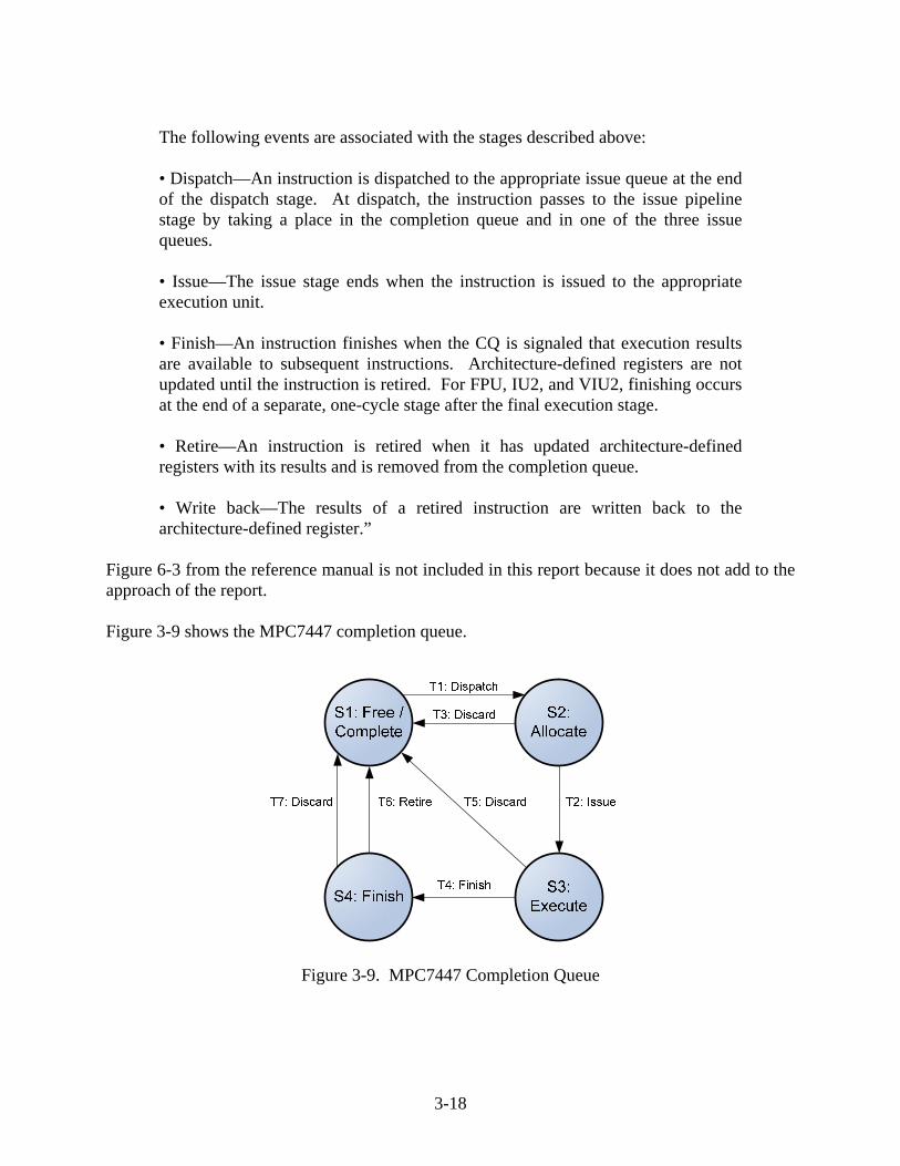
Figure 6-3 from the reference manual is not included in this report because it does not add to the approach of the report. Figure 3-9 shows the MPC7447 completion queue.
Figure 3-9. MPC7447 Completion Queue
3-18

The FSM state description is as follows: • S1: Free/Complete—Default state. No pending instructions. • S2: Allocate—Instruction is currently in issue pipeline. • S3: Execute—Execution units are currently processing instruction. • S4: Finish—Execution results are ready. Registers are being updated. The FSM transition description is as follows: • T1: Dispatch—Instruction is dispatched to the appropriate issue queue.
• T2: Issue—Instruction and operands are latching into appropriate reservation station.
• T3: Discard—Instruction follows an instruction that causes exception, or flush instruction issued, causing a discard.
• T4: Finish—Execution results are available to subsequent instructions; CQ signals this event.
• T5: Discard—Instruction follows an instruction that causes exception, or flush instruction issued, causing a discard.
• T6: Retire—Instruction has updated registers with execution results.
• T7: Discard—Instruction follows an instruction that causes exception, or flush instruction issued, causing a discard.
3.5.1.4.2 Critical Buffer: Rename Buffer. Source Documentation—MPC7450 RISC Microprocessor Family Reference Manual, pg. 6-3 [9]:
“Rename registers—Temporary buffers for holding results of instructions that have finished execution but have not completed.”
A Buffer-Oriented Methodology for Microarchitecture Validation, pg. 55 [7]:
“An entry is Free until the dispatch unit allocates an entry for an instruction in the dispatch stage. This occurs if an instruction modifies any register. The entry remains allocated until the instruction completes and the result is written back to the register file. There are two states for an allocated entry. At the time of renaming, each newly allocated rename entry will always hold the most recent (MR) value for the renamed register denoted by the MR Allocate state of Fig. 7. If a rename entry is allocated to a register which is then later renamed by another instruction, the previously allocated entry will no longer hold the most recent value and will therefore transition from the MR Allocate state to the NonMR
3-19

Allocate state. Once the instruction finishes, the content of the rename entry becomes valid which causes a transition from MR Allocate (NonMR Allocate) to MR Valid (NonMR Valid). The FSM stays in the valid state until the result is written to the register file (WB transition) or a prior instruction causes an exception that requires all subsequent instructions to be discarded (discard transition).”
Figure 3-10 shows the MPC7447 rename buffer.
Figure 3-10. MPC7447 Rename Buffer The FSM state description is as follows: • S1: Free—Default state. No pending instructions.
• S2: MR Allocate—Entry holds most recent (MR) value.
• S3: MR Valid—Instruction is finished. MR value is valid.
• S4: NonMR Allocate—Subsequent instruction has renamed associated register. Entry value is no longer most recent (NonMR).
• S5: NonMR Valid—Instruction is finished. NonMR value is valid.
The FSM transition description is as follows: • T1: Dispatch—Newly dispatched instruction requires register renaming, entry holds
most recent value.
3-20

• T2: Finish—Completion unit retires instruction.
• T3: Stale—A subsequent instruction renames this register, current entry does not hold most recent value.
• T4: Write Back—Completed result is written back to register file.
• T5: Stale—A subsequent instruction renames this register, current entry does not hold most recent value.
• T6: Finish—Completion unit retires instruction.
• T7: Write Back—Completed result is written back to register file.
• T8: Discard—Not pictured. Prior instruction causes an exception that requires all subsequent instructions to be discarded.
3.5.1.4.3 Critical Buffer: Reservation Station. Source Documentation—MPC7450 RISC Microprocessor Family Reference Manual, pg. 6-3 [9]:
“Reservation station—A buffer between the dispatch and execute stages that allows instructions to be dispatched even though the results of instructions on which the dispatched instruction may depend are not available.”
Figure 3-11 shows the MPC7447 reservation station.
Figure 3-11. MPC7447 Reservation Station
3-21

The FSM state description is as follows: • S1: Free—Default state. No pending instruction. • S2: Allocate Non-Valid—A pending instruction is awaiting its operand(s). • S3: Allocate Valid—A pending instruction has all operands, and is ready to execute. The FSM transition description is as follows: • T1: Allocate—Dispatch Unit allocates entry, operand(s) not available.
• T2: Discard—Instruction follows an instruction that causes exception, or flush instruction issued, causing a discard.
• T3: Operand Valid—Operand(s) for allocated instruction are available.
• T4: Allocate—Dispatch Unit allocates, entry, operand(s) available.
• T5: Issue—Instruction is issued.
• T6: Discard—Instruction follows an instruction that causes exception, or flush instruction issued, causing a discard.
3.5.2 Freescale MPC8540. 3.5.2.1 Feature 1—Load/Store Unit.
3.5.2.1.1 Critical Buffer: Load Miss Queue. Source Documentation—PowerPC e500 Core Family Reference Manual, pg. 4-26, table 4-1 [11]:
“As loads reach the LSU, it tries to access the cache. On a hit, the cache returns the data. If there is a miss, the LSU allocates an LMQ entry and a DLFB entry. The LSU then queues a bus transaction to read the line. If a subsequent load hits, the cache returns the results. If a subsequent load misses, the LSU allocates a second LMQ entry and, if the load is to a different cache line than the outstanding miss, it allocates the second DLFB entry and queues a second read transaction on the bus. If the load miss is to the same cache line as an outstanding miss, the LSU need not allocate a new DLFB entry. The LSU continues processing load hits and load misses until one of the following conditions occurs: • The LMQ is full and another load miss occurs. • The LSU tries to perform a load miss, all of the DLFB entries are full, and the load is not to any of the cache lines that are represented in the DLFB.”
3-22

Figure 3-12 shows the MPC8540 LMQ.
Figure 3-12. MPC8540 Load Miss Queue The FSM state description is as follows: • S1: Free—Default state. No pending load instructions.
• S2: Allocated—This entry currently contains a pending load instruction that is awaiting data due to a cache miss.
The FSM transition description is as follows: • T1: L1 Cache Miss—LSU receives load instruction, cache miss occurs. • T2: Complete—Data returns from L2 cache, L3 cache, or the system bus. 3.5.2.1.2 Critical Buffer: L1 Store Queue. Source Documentation—PowerPC e500 Core Family Reference Manual, pg. 4-26, table 4-1 [11]:
“Stores cannot execute speculatively and are held in the seven-entry store queue, shown in Figure 4-10, until completion logic indicates that the store instruction is to be committed. The store queue arbitrates for L1 data cache access. When arbitration succeeds, data is written to the data cache and the store is removed from the store queue. If a store is caching-inhibited, the operation moves through the store queue to the rest of the memory subsystem.”
3-23

Figure 3-13 shows the MPC8540 L1 store queue.
Figure 3-13. MPC8540 L1 Store Queue The FSM state description is as follows: • S1: Free—Default state. No pending store instructions.
• S2: Allocated—A pending store instruction has all required operands and is being executed.
• S3: Store Cache-Inhibited—The corresponding CI store data is waiting to enter the memory subsystem.
• S4: Store Cacheable—The corresponding cacheable store data is waiting to enter the L1 cache.
The FSM transition description is as follows: • T1: Store—LSU receives store instruction. • T2: Cache-Inhibited Store—LSU receives store instruction. Store is cache-inhibited. • T3: Completed—Store is transferred to Memory Subsystem. • T4: Cacheable Store—LSU receives store instruction. Store is cacheable. • T5: Cache Updated—L1 cache is updated. 3.5.2.1.3 Critical Buffer: Data Write Buffer. Source Documentation—PowerPC e500 Core Family Reference Manual, pg. 4-27, table 4-1 [11]:
3-24

“When a full line of data is available in the DLFB, the data cache is updated. If a data cache update requires a cache line to be evicted, the line is cast out and placed in the DWB until the data has been transferred through the core interface unit to the core complex bus. If global memory’s coherency needs to be maintained as a result of bus snooping, the L1 cache can also evict a line to the DWB. (This is a snoop push.) Cast-out and snoop push writes from the L1 cache are cache-line aligned (critical word is not written first), regardless of which word in a modified cache line is accessed. One DWB entry is dedicated for snoop pushes, one is for cast outs, and one can be used for either.”
Figure 3-14 shows the MPC8540 data write buffer.
Figure 3-14. MPC8540 Data Write Buffer The FSM state description is as follows: • S1: Free—Default state. No data has been selected as a castout from the L1 cache.
• S2: Write Back—Modified data is being written back to the L2 cache, L3 cache, or memory subsystem.
• S3: Allocated—Data has been selected for castout from the L1 cache.
• S4: Free—Default state. No pending cache push operation.
• S5: Allocated—Snoop hit occurred, entry is holding a pending cache push operation.
The FSM transition description is as follows: • T1: PLRU Castout—L1 cache update requires cache line eviction.
3-25

• T2: Free Entry—Cast out line is clean, no write-back required.
• T3: Commit—Cast out line is dirty, data needs to be updated in L2 cache, L3 cache, and/or system bus.
• T4: Free Entry—Cast out line is dirty, data is written back.
• T5: Snoop Hit—Modified cache line detects snoop hit from another bus master.
• T6: Complete—Modified data is transferred to the L1 cache, L2 cache, L3 cache, or memory subsystem.
3.5.2.1.4 Critical Buffer: Data Line Fill Buffer. Source Documentation—PowerPC e500 Core Family Reference Manual, pg. 4-27, table 4-1 [11]:
“DLFB entries are used for loads and cacheable stores. Stores are allocated in the DLFB so loads can access data from the store immediately (loads cannot access data from the L1 store queue). Also, by using the DLFB entries for stores, the LSU frees L1 store queue entries, even on store misses. Multiple cacheable store misses to the same cache line are merged in a DLFB.”
Figure 3-15 shows the MPC8540 data line fill buffer.
Figure 3-15. MPC8540 Data Line Fill Buffer
3-26

The FSM state description is as follows: • S1: Free—Default state. No pending load or store instructions.
• S2: Allocated Store—A pending store instruction has all required operands and is being executed.
• S3: Merge—Newly modified data for a pending store instruction will be written to cache.
• S4: Allocated Load—This entry currently contains a pending load instruction that is awaiting data due to a cache miss.
The FSM transition description is as follows: • T1: Store—LSU receives store instruction.
• T2: Store to Same Cache Line—LSU receives another store instruction to the same cache line.
• T3: Cache Updated—L1 cache is updated.
• T4: Cache Updated—L1 cache is updated.
• T5: Load Miss—LSU Receives load instruction, cache miss occurs.
• T6: Complete—Data returns from L2 cache, L3 cache, and/or the system bus.
3.5.2.2 Feature 3—L1 Cache.
3.5.2.2.1 Critical Buffer: MESI Cache Coherency. Source Documentation—PowerPC e500 Core Family Reference Manual, pg. 11-10 [11]:
“Each 32-byte data cache block contains status bits that define the MESI state of the cache line. The core complex uses these bits to support coherency protocols and to direct reload operations. Table 11-1 describes data cache states.”
3-27

Table 11-1. Cache Line State Definitions
Status Bits Name Description 101 Modified (M) The line is in the cache and has been modified with
respect to main memory. It does not reside in any other coherent caches.
100 Exclusive (E) This line is present in the cache, and this cache has exclusive ownership of the line. It is not present in any other coherent cache and it is the same as main memory. This processor may subsequently modify this line without notifying other bus masters.
110 Shared (S) The addressed line is in the cache, it may be in another coherent cache, and it is the same as main memory. It cannot be modified by any processor.
0xx Invalid (I) The cache location does not contain valid data. Figure 3-16 shows the MPC8540 MESI cache coherency.
S3: SharedS4: Invalid
S2: Exclusive
S1: Modified
T10: Snoop Write Hit
T12: Snoop Write Miss
T8: Snoop Read Hit
T9: P
roc
Rea
d H
it
T2: S
noop
Writ
e H
it
T14:
Pro
c W
rite
Mis
s
T7: S
noop
Rea
d H
it
T4: Proc Read HitT1: Proc Rd/Wr Hit
T5: Proc Rd/Wr Hit
T11: P
roc W
rite H
it
T3: Sno
op R
ead H
it
T13: Proc Read MissT6: Snoop Write Hit
Figure 3-16. MPC8540 MESI Cache Coherency The FSM state description is as follows: • S1: Modified—The line is in the cache and has been modified with respect to main
memory. It does not reside in any other coherent caches.
3-28

• S2: Exclusive—This line is present in the cache, and this cache has exclusive ownership of the line. It is not present in any other coherent cache, and it is the same as main memory. This processor may subsequently modify this line without notifying other bus masters.
• S3: Shared—The addressed line is in the cache, it may be in another coherent cache, and it is the same as main memory. It cannot be modified by any processor.
• S4: Invalid—The cache location does not contain valid data.
The FSM transition description is as follows: • T1: Processor Read/Write Hit—Processor cache read/write hit detected. • T2: Snoop Write Hit—Snooping cache write hit detected. • T3: Snoop Read Hit—Snooping cache read hit detected. • T4: Processor Read Hit—Processor cache read hit detected. • T5: Processor Read/Write Hit—Processor cache read/write hit detected. • T6: Snoop Write Hit—Snooping cache write hit detected. • T7: Snoop Read Hit—Snooping cache read hit detected. • T8: Snoop Read Hit—Snooping cache read hit detected. • T9: Processor Read Hit—Processor cache read hit detected. • T10: Snoop Write Hit—Snooping cache write hit detected. • T11: Processor Write Hit—Processor cache write hit detected. • T12: Snoop Write Miss—Snooping cache write miss detected. • T13: Processor Read Miss—Processor cache read miss detected. • T14: Processor Write Miss—Processor cache write miss detected. 3.5.2.3 Feature 4—Branch Prediction Unit.
3.5.2.3.1 Critical Buffer: Branch History Table. Source Documentation—PowerPC e500 Core Family Reference Manual, pg. 10-2 [11]:
“…each with a 2-bit, dynamically updated branch history table that indicates four levels of likelihood that the branch will be taken (strongly taken, taken, not taken, strongly not taken).”
Computer Architecture: A Quantitative Approach, pg. 198 [10]:
“The 2-bit [branch prediction] scheme is actually a specialization of a more general scheme that has an n-bit saturating counter for each entry in the prediction buffer. With an n-bit counter, the counter can take on values between 0 and 2n – 1: When the counter is greater than or equal to one-half of its maximum value (2n – 1), the branch is predicted as taken; otherwise, it is predicted untaken. As in the
3-29

2-bit scheme, the counter is incremented on a taken branch and decremented on an untaken branch.”
Figure 3-17 shows the MPC8540 branch history table.
S3: Not-TakenS2: Taken
S4: Strongly
Not-Taken
S1: Strongly Taken
T7: RT T1: RNT T3: RNT T5: RT
T2: RNT
T6: RT
T8: RT T4: RNT
Figure 3-17. MPC8540 Branch History Table The FSM state description is as follows: • S1: Strongly Taken—BPU prediction will be Taken. • S2: Taken—BPU prediction will be Taken. • S3: Not-Taken—BPU prediction will be Not-Taken. • S4: Strongly Not-Taken—BPU prediction will be Not-Taken. The FSM transition description is as follows: • T1-4: Resolved Not-Taken (RNT)—The corresponding conditional branch instruction has
resolved to not-taken.
• T5-8: Resolved Taken (RT)—The corresponding conditional branch instruction has resolved to taken.
3-30

3.5.2.4 Feature 5—Out-of-Order Execution.
3.5.2.4.1 Critical Buffer: Completion Queue. Source Documentation—PowerPC e500 Core Family Reference Manual, pg. 4-9,10 [11]:
“Fetch—Instructions are fetched from memory and placed in the 12-entry IQ. The latency associated with accessing an instruction depends on whether the instruction is in the on-chip cache or system memory (in which case latency is further affected by bus traffic, bus clock speed, and address translation issues). Therefore, in the examples in this chapter, the diagrams and fetch stage shown is for the common case of instructions hitting in the instruction cache. Decode—As many as two eligible instructions dispatch from IQ0–IQ1 to the appropriate issue queue. Note that isync, rfi, sc, and some other instructions do not go to issue queues. At the same time, the instruction is assigned an entry in the completion queue. Issue—Instructions are dispatched to issue queues from the instruction queue entries. At the end of the issue stage, instructions and their operands, if available, are latched into execution unit reservation stations. The black stripe is a reminder that the instruction occupies an entry in the CQ, described in Figure 4-4. Execute—The operations specified by an instruction are being performed by the appropriate execution unit. The black stripe is a reminder that the instruction occupies an entry in the CQ, described in Figure 4-4. Complete—Execution has finished. When all completion requirements are met, the instruction is retired from the CQ. The results are written back to architecture-defined registers in the clock cycle after retirement. Write back—The instruction has retired and its results are written back to the architecture-defined registers. The events are described as follows: • Dispatch (at the end of decode)—An instruction is dispatched to the appropriate issue queue at the end of the decode stage. At dispatch, the instruction passes to the issue pipeline stage by taking a place in the CQ and in one of the two issue queues. • Issue (at the end of the issue stage)—The issue stage ends when the instruction is issued to the appropriate execution unit.
3-31

• Finish (at the end of the execute stage)—An instruction finishes when the CQ is signaled that execution results are available to subsequent instructions. Architecture-defined registers are not updated until the instruction is retired. • Retire (at the end of the complete stage)—An instruction retires from the CQ after execution is finished and serializing conditions are met. • Write back (at the end of the write-back stage)—The results of a retired instruction are written back to the architecture-defined register.”
Figure 4-4 from the reference manual is not included in this report because it does not add to the approach of this report. Figure 3-18 shows the MPC8540 completion unit.
Figure 3-18. MPC8540 Completion Unit The FSM state description is as follows: • S1: Free/Complete—Default state. No pending instructions. • S2: Allocate—Instruction is currently in issue pipeline. • S3: Execute—Execution units are currently processing instruction. • S4: Finish—Execution results are ready. Registers are being updated. The FSM transition description is as follows: • T1: Dispatch—Instruction is dispatched to the appropriate issue queue.
• T2: Issue—Instruction and operands are latching into appropriate reservation station.
• T3: Discard—Instruction follows an instruction that causes exception, or flush instruction issued, causing a discard.
3-32
• T4: Finish—Execution results are available to subsequent instructions; CQ signals this event.
• T5: Discard—Instruction follows an instruction that causes exception, or flush instruction issued, causing a discard.
• T6: Retire—Instruction has updated registers with execution results.
• T7: Discard—Instruction follows an instruction that causes exception, or flush instruction issued, causing a discard.
3.5.2.4.2 Critical Buffer: Rename Buffer. Source Documentation—MPC7450 RISC Microprocessor Family Reference Manual, pg. 6-3 [9]:
“Rename registers—Temporary buffers for holding results of instructions that have finished execution but have not completed.”
A Buffer-Oriented Methodology for Microarchitecture Validation, pg. 55 [7]:
“An entry is Free until the dispatch unit allocates an entry for an instruction in the dispatch stage. This occurs if an instruction modifies any register. The entry remains allocated until the instruction completes and the result is written back to the register file. There are two states for an allocated entry. At the time of renaming, each newly allocated rename entry will always hold the most recent (MR) value for the renamed register denoted by the MR Allocate state of Fig. 7. If a rename entry is allocated to a register which is then later renamed by another instruction, the previously allocated entry will no longer hold the most recent value and will therefore transition from the MR Allocate state to the NonMR Allocate state. Once the instruction finishes, the content of the rename entry becomes valid which causes a transition from MR Allocate (NonMR Allocate) to MR Valid (NonMR Valid). The FSM stays in the valid state until the result is written to the register file (WB transition) or a prior instruction causes an exception that requires all subsequent instructions to be discarded (discard transition).”
3-33

Figure 3-19 shows the MPC8540 rename buffer.
Figure 3-19. MPC8540 Rename Buffer
The FSM state description is as follows: • S1: Free—Default state. No pending instructions.
• S2: MR Allocate—Entry holds most recent (MR) value.
• S3: MR Valid—Instruction is finished. MR value is valid.
• S4: NonMR Allocate—Subsequent instruction has renamed associated register. Entry value is no longer most recent (NonMR).
• S5: NonMR Valid—Instruction is finished. NonMR value is valid.
The FSM transition description is as follows: • T1: Dispatch—Newly dispatched instruction requires register renaming, entry holds
most recent value.
• T2: Finish—Completion unit retires instruction.
• T3: Stale—A subsequent instruction renames this register, current entry does not hold most recent value.
• T4: Write Back—Completed result is written back to register file.
3-34

• T5: Stale—A subsequent instruction renames this register, current entry does not hold most recent value.
• T6: Finish—Completion unit retires instruction.
• T7: Write Back—Completed result is written back to register file.
• T8: Discard—Not pictured. Prior instruction causes an exception that requires all subsequent instructions to be discarded.
3.5.2.4.3 Critical Buffer: Reservation Station. Source Documentation—PowerPC e500 Core Family Reference Manual, pg. 4-3 [11]:
“Reservation station—A buffer between the issue and execute stages that allows instructions to be issued even though resources necessary for execution or results of other instructions on which the issued instruction may depend are not yet available.”
Figure 3-20 shows the MPC8540 reservation station.
Figure 3-20. MPC8540 Reservation Station The FSM state description is as follows: • S1: Free—Default state. No pending instruction. • S2: Allocate Non-Valid—A pending instruction is awaiting its operand(s). • S3: Allocate Valid—A pending instruction has all operands and is ready to execute.
3-35

The FSM transition description is as follows: • T1: Allocate—Dispatch Unit allocates entry, operand(s) not available.
• T2: Discard—Instruction follows an instruction that causes exception, or flush instruction issued, causing a discard.
• T3: Operand Valid—Operand(s) for allocated instruction are available.
• T4: Allocate—Dispatch unit allocates, entry, operand(s) available.
• T5: Issue—Instruction is issued.
• T6: Discard—Instruction follows an instruction that causes exception, or flush instruction issued, causing a discard.
3.6 COVERAGE RESULTS. The gathering coverage results for BOMV-based tests was not completed in Phase 2. Refer to appendix B for more details on the coverage metrics required and the status of building confidence in BOMV. 3.7 FEATURE VERIFICATION. In this phase of the project, the research team was unable to apply the Feature Verification stage due to time constraints. The Feature Verification step of this framework will be studied and tested more thoroughly in the next phase of this project. Proper feature verification requires that sufficient confidence in the verification methodology exists. Currently, the feature verification methodology proposed is being assessed for completeness and accuracy. Successful feature verification will allow system verification engineers to ensure that a COTS microprocessor conforms to its specification. 3.8 FEATURE RISK ANALYSIS. In this phase of the project, the research team was unable to apply the Feature Risk Analysis stage due to time constraints. The Feature Risk Analysis step will go through complete specification in the next phase of this project. This will involve the cooperative guidance of the PMC members to ensure that the formulation of the risk assessment of a COTS microprocessor meets the safety requirements set forth by the FAA. Currently, this risk assessment formulation depends on the microarchitecture feature risks and the results of feature verification.
3-36

4. SAFETY PROCESS FOR SoC.
4.1 OVERVIEW. Using SoCs will be predominant in future aerospace systems. Safety analysis of these complex designs is more complicated than of COTS microprocessors due to extensive IP reuse. These are usually composed of processor cores and other complex IP cores such as interface controllers, on-chip interconnects, coprocessors, on-chip memory, and memory controllers. The task of ascertaining the safety considerations of SoCs is further complicated by the variety of designs. Unlike the case of COTS microprocessors, where the majority of features of interest are similar across microprocessors, SoC components tend to vary based on the product selected, making safety analysis more complicated. Not only are the safety concerns due to the individual IP cores an issue, but interaction among them presents a verification challenge to the system designers. Certain systems using SoCs may not require particular on-chip core and, for safety reasons, would require the disabling of that core. These issues need to be considered when formulating a safety assessment process for SoCs. The following sections present a four-step process documenting four aspects of SoCs critical to the safety of the systems into which they are deployed. 4.2 THE SoC SAFETY PROCESS STEPS. Assessing the safety of SoCs involves identification of cores that compose the SoC. Determining accessibility of cores via SoC interfaces is critical towards formulating a safety assessment plan for a particular on-chip core. Interaction among cores may contribute to an unsafe state in the SoC and should be exhaustively studied. Isolating on-chip cores may be desirable in particular system configurations and must be assessed. The following sections discuss these aspects in further detail. 4.2.1 Core Identification. This step involves the identification of on-chip cores in the SoC selected for approval. Identifying the variety of on-chip cores allows system designers to establish the necessary steps needed to complete the analysis. Processing elements, interface controllers, on-chip memory, on-chip interconnects, and any other on-chip components are just some of the varieties that need to be identified and documented. This process is accomplished by studying the available documentation listed in section 4.4. 4.2.2 Core Accessibility. For the safety analysis of SoCs, it is critical to ascertain the accessibility constraints of all on-chip cores. Accessibility may vary for both stimulation with test vectors and observation of the outputs once vectors are applied. The accessibility of one core may be dependent on other cores. For example, when testing on-chip cache, the processor executes test programs that populate the
4-1

cache allowing the test. This dependence in accessibility must be identified and documented. Accessibility also has an impact on the test for core interaction and core isolation. As with traditional circuit testing, focus is placed on the observability and controllability aspects of the SoC and its IP core components. Observability is defined as the ease or difficulty in observing the state of a particular logic device (IP core), while controllability refers to the ease or difficulty of setting the state in a particular logic device (IP core). These principles are also applicable to IP core testing. 4.2.3 Core Interaction. Higher levels of integration in SoCs prevent the visibility of transactions within the SoC infrastructure. Ensuring that operation of the SoC is safe requires guaranteeing that communication and interaction between cores is limited to the specified entities and does not affect other cores. Documenting core interaction of the SoC selected for approval aids system designers in formally identifying possible issues to safety. This process involves the following activities: • Identify communicating partners in the SoC • Determine the types of communications between these communicating partners • Develop a core interaction graph (CIG) highlighting these communicating partners • Generate a sequence of tests to validate correct operation between communicating
partners 4.2.4 Modeling the Core Interaction. Core interaction is modeled with the help of a CIG. The nodes of the CIG represent IP cores, while the directional edges indicate possible communication (data and control) between the cores. The purpose of this type of modeling is to formally identify the interaction aspects that need to be assessed when qualifying SoC. As a special note: • External inputs also contribute to edges on the cores. • Components on the bus tend to form cliques, since there is a possibility of
communication—intentional and inadvertent.
4-2

4.2.5 Generating Test Sequences. After identifying the interactions among IP cores, test programs to exercise and verify these interactions have to be developed. Test programs will have to ensure that only communicating cores are involved in the interactions and that other cores are not modified. Core accessibility concerns regarding the observability and controllability of IP cores and their dependents need to be considered. 4.2.6 Core Isolation. Since SoCs may provide more cores than what is actually required by the system in which it is deployed, the designer may want the ability to disable or isolate a particular core. The Core Accessibility and Core Interaction steps need to be considered. The ability to disable a particular core needs to be documented and demonstrated using a set of test programs. Inputs into the SoC should not affect disabled cores. Using the Core Accessibility and Core Interaction details ensure that disabled cores are not affected once isolated. This is achieved by ensuring that any changes in core interaction with disabled cores does not affect the disabled core state. 4.3 THIRD-PARTY TOOLS AND EVALUATION BOARDS. Third-party tools and evaluation boards may also be available from vendors, which may be used for debugging certain components (i.e., processors, interfaces, controllers, etc.) of the SoC. Using SoCs, system designers need to identify available third-party tools and assess their capabilities and limitations. 4.4 REFERENCE DOCUMENTATION. The types of documentation typically available from vendors and the information they provide are listed below. 1. Reference manual:
a. Reliability and quality information b. Programming environment c. Programming interface d. Feature specifications e. Modes of operation
2. User guide:
a. Programming model b. Cache operation c. Exceptions
4-3

d. Memory management e. Instruction timing f. Emerging features (i.e., AltiVec/Performance Monitors) g. Signal descriptions h. System interface operations i. Power management j. Instruction set listing k. Document revision status
3. Data sheets:
a. Feature summary b. Electrical characteristics c. Power characteristics d. Clock configuration e. Reset initialization f. Memory characteristics g. Features operating specifications h. Interfaces operating specifications i. Thermal specifications j. Design information k. Pin assignments l. Packaging description n. Ordering information
4. Errata documents:
a. Errata revision level to part marking cross reference b. Summary table of all known errata and cross reference to silicon revision level c. Detailed errata information
– Errata number – Overview – Detailed description – Project impacts – Work-arounds – Projected solution
5. Application notes: These typically demonstrate how particular features are used.
Example code sequences are usually provided to illustrate the same. 6. White papers 7. Mechanical packaging
4-4

8. Roadmaps 9. Product change notices 10. Models
a. BSDL—Boundary-Scan Description Language (language used in design of electronic test logic)
b. Bus functional models
c. Full functional models
d. IBIS—I/O Buffer Information Specification. A format for defining the analog characteristics of the input and output of integrated circuits. IBIS models are ASCII files that provide the behavioral information required to model the device without divulging the proprietary design of the circuit.
e. Timing models
11. References to third-party companion chips and third-party software support.
4-5/4-6

5. SAFETY PROCESS PRODUCTS FOR SoC. 5.1 PRODUCT OVERVIEW—MPC8540. In Phase 1, two microprocessors were selected as candidates for this research: Freescale MPC7447 and Freescale MPC8540. The MPC8540 is an SoC, and this section presents products developed during the implementation of the process steps. 5.2 CORE IDENTIFICATION. Using the reference documentation available from the manufacturer, the following on-chip cores were identified for the MPC8540. 1. e500 processor core 2. e500 Coherency Module (ECM) 3. OCeaN on-chip network 4. DMA controller 5. RapidIO interface controller 6. Peripheral component interconnect-extended (PCI-X) controller 7. Embedded Programmable Interrupt Controller 8. Interintegrated circuit (I2C) 9. Double data rate (DDR) memory controller 10. General-Purpose Chip-Select Machine 11. On-chip cache 12. Ethernet™ controllers 13. Dual Universal Asynchronous Receiver Transmitter (DUART) 14. Local Bus Controller (LBC) 15. JTAG boundary scan 5.3 CORE ACCESSIBILITY. Table 5-1 summarizes the core accessibility for MPC8540.
Table 5-1. Core Accessibility Summary for MPC8540
No. Core Reference Document Comments
1 e500 processor core
– Programs to be executed need to be loaded into the instruction memory and then executed. These programs would be determined in the Microprocessor Safety Process.
2 ECM MPC8540RM (reference 12)
Configuration registers are specified along with individual fields.
5-1

Table 5-1. Core Accessibility Summary for MPC8540 (Continued)
No. Core Reference Document Comments
3 OCeaN on-chip network
– Insufficient documentation is available on this feature.
4 DMA controller MPC8540RM (reference 12)
Reference 12 provides modes of operation, signal description, memory map, and register specification.
5 RapidIO interface controller
AN2923 (reference 13), AN2741 (reference 14), AN2753 (reference 15)
Sample application code to be run in conjunction with U-Boot, for proving functionality of messaging unit. AN2753 also provides bring-up procedure for the PowerQUICC.
6 PCI-X controller MPC8540RM (reference 12)
Debug interface provided. See Section 20.4.2 – “PCI/PCI-X Interface Debug” in reference 12.
7 EPIC MPC8540RM (reference 12)
PIC specification: signal inputs, outputs provided in reference 12.
8 I2C MPC8540RM (reference 12)
Reference 12 provides signal information, configuration register information, I2C modes of operation.
9 PowerQUICC III DDR memory controller
AN2583 (reference 16)
This document provides programming guidelines for using the memory controller.
11 On-chip cache (DDR SDRAM)
MPC8540RM (reference 12)
Debug interface provided. See Section 20.4.3—“DDR SDRAM Interface Debug” in reference 12.
12 Ethernet Controller (TSEC—triple speed ethernet controller)
AN2925 (reference 17), AN2745 (reference 18)
AN2925 provides software for TSEC initialization. AN2745 demonstrates how to set-up TSEC hash tables.
13 DUART MPC8540RM (reference 12)
Reference manual describes registers to be modified for DUART control.
14 LBC MPC8540RM (reference 12)
Debug interface provided. See Section 20.4.4—“Local Bus Interface Debug” in reference 12.
DDR = Double data rate PIC = Programmable interrupt controller SDRAM = Synchronous Dynamic Random-Access Memory TSEC = Triple speed Ethernet controller
5-2

Due to the lack of available documentation on core accessibility, the evaluation of the SoC Safety Process and a report on artifacts and products generated from applying the SoC Safety Process to the Freescale MPC8540 is currently incomplete and will be completed in Phase 3. Because there was only access to the publicly available reference manual for the MPC8540, it was not possible to fully apply the SoC Safety Process. Specifically, it was not possible to complete the core accessibility step of the SoC Safety Process due to a lack of information. Other details to be included in this research are identifying other cores involved in the accessibility of any given core. 5.4 CORE INTERACTION. Using reference 12, possible interactions between the on-chip components were identified and represented using the CIG discussed in section 4.2.3. In figure 5-1, the clique is represented as a single unit to provide a cleaner view of the interactions. The elements of this clique are attached to a single on-chip bus, presenting additional safety challenges to core isolation and core interaction.
L2-Cache
5.5 CORE ISOLATION. Core isolation will be completed in a following phase of this project.
DMA Controller
PCI Controller
RapidIO Controller
OCeaN
ECM e500 core
I2C Controller
TSEC
LBC
TSEC
CLIQUE
DUART
PIC
ENET
SDRAM Controller
Figure 5-1. Core Interaction Graph for MPC8540
5-3

5.6 THIRD-PARTY TOOLS AND EVALUATION BOARDS. The QUICCStart MPC8540 Evaluation System platform allows for the evaluation of target applications for the MPC8540 system. Initial experiments with the board allowed access to register and memory content, allowing for processor core evaluation. Further experimentation is needed to assess its capability in analyzing other on-chip cores.
5-4

6. UNTAKEN PATHS. 6.1 OVERVIEW. This section discusses some options identified by the research staff. 6.2 TOOLS. Manufacturers typically use in-house verification and validation tools. These use the complete knowledge of the microprocessor design for configuring tools to generate test vectors, i.e., test instruction sets, for testing. With limited availability of microprocessor design information, the research staff explored the possibility of using third-party test generation tools to generate necessary test programs. Two such tools were identified and are discussed in the following sections. 6.2.1 Genesys and Genesys-Pro. Genesys (IBM Haifa Research Lab) [19] is a model-based, pseudo-random, state-of-the-art test generator that dynamically generates tests using a generation-simulation cycle for each instruction. Its primary aim is to enable the implementation of comprehensive verification plans. Genesys gives the user control to guide the generation of test programs, which range from completely deterministic to totally random. The model-based structure of Genesys makes it applicable to any architecture, which is one of its most significant characteristics. Clearly, this structure also makes it easy to implement and maintain common architecture changes and upgrades. Another important asset is the fact that the structure of Genesys allows for the external incorporation of complex testing knowledge, which represents accumulated testing-engineer expertise. Users can add this knowledge in an incremental and localized manner, thereby providing a virtually unlimited generation platform, in terms of scope and smartness. 6.2.2 RAVEN. RAVEN (Random Architecture Verification Engine) (Obsidian Software, Austin, TX) is a random test generator (RTG) for functional verification of complex processors. The tool provides a biased RTG for a set of microprocessor architectures (the MIPS32, MIPS64, x86-Pentium 4, and ARMx family). A brief introduction regarding how RAVEN can be used in a design environment for processor verification is given in reference 20. Note that this RTG is meant to be used by microprocessor vendors to allow for design verification. A list of the microprocessor features handled by the tool is enumerated in reference 21. 6.3 QUALITY METRICS. With current SoC design trends focusing around IP reuse, manufacturers are investigating techniques to reduce verification overheads prior to IP integration. Quality metrics can aid system integrators in making informed decisions regarding the quality of the chosen IP core.
6-1

The VSI Alliance (VSIA) Quality IP (QIP) Metric [22] is a tool that can aggressively reduce the time typically required to make an IP purchase decision and to integrate the core. The VSIA QIP Metric helps the IP vendor and the consumer communicate based on an objective foundation. Besides setting up the basis for measuring a core’s characteristics against an industry-approved list of attributes, the QIP Metric provides a view of the IP vendor’s general approach to IP development. This enables a continuous improvement mechanism, and in turn, levels the playing field for vendors and allows an integrator to evaluate similar cores from competing vendors. In Version 2.0, the VSIA QIP Metric is more streamlined and easier to use than its predecessor. This version also has simpler IP-qualification metrics covering documentation, deliverables, and information specific to the IP integrator as well as IP development practices. The VSIA QIP Metric 2.0 includes the newly added vendor assessment, and the requirements for Soft IP have been restructured and revisited. This VSIA QIP Metric was proposed primarily for the purpose of SoC design and IP integration. In the proposed process, this VSIA QIP Metric could also be used to give the system design the ability to decide on the feasibility of using a specific SoC design containing particular IP cores. Specific sections that are of interest in the VISA QIP Metric worksheets include the following: • 2.1: Design Quality, Verification Documentation
This section examines the quality of the test plan documentation from the manufacturer. It examines coverage targets, tool and platform configurations, IP verification environment, test bench documentation, verification steps for the IP integrator, and reuse of test documentation for system-level integration.
• 2.3: Verification Quality
This section takes a detailed look at coverage, simulation messaging, verification environment, verification components, and formal methods of verification.
6.4 SoC TESTERS. The research team identified the possibility of using SoC testers to aid in the safety assessment of SoCs. These are used by SoC manufacturers in the verification of their designs. The Advantest T6682 SoC tester is owned by an AFE#43 team member and is intended for use on a radiation-hardened IBM PowerPC microprocessor. The cost of SoC testers is a major hurdle during safety assessment, with typical costs around $4 million. The aspect of safety assessment can be further explored, given access to such testers.
6-2

7. CONCLUSIONS. 7.1 SUMMARY. Avionics system developers BAE Systems, The Boeing Company, Lockheed Martin, and Smiths Aerospace joined with the Federal Aviation Administration (FAA) in sponsoring this research at Texas A&M University. The purpose was to develop the techniques and methodologies to integrate industry approaches to using the evolving microprocessor technology in future avionics and safety-critical applications. This project offered a laboratory for both industry and the FAA to meld their composite requirements and evaluate new technologies and evolving commercial off-the-shelf (COTS) microprocessors for any impact on safety. The output may be used by the FAA to develop regulatory policy, guidelines, and procedures for safety. This project considers the applicability of RTCA/DO-254 and RTCA/DO-178B to microprocessors, documents potential safety concerns when using modern microprocessors on aircraft, and proposes potential approaches for addressing those safety concerns. Both ground and airborne avionics are dependent upon the use of COTS microprocessors. Evolving microprocessor architectures include concepts such as caching, pipelining, and other advanced features that can affect system performance, predictability, and safety. Qualification and certification policy and procedures of safety-critical avionics require proof of safety. There is a risk of these regulatory activities becoming exorbitantly expensive and less effective in ensuring safety requirements are met. Microprocessors (including systems-on-a-chip (SoCs)) are driven by market forces that generally do not consider avionics safety requirements and are rushed into production to meet competitive goals. Due to the need to select COTS components that are less expensive, meet evolving system requirements, and are still being produced and maintained by the manufacturers, designers, and integrators, maintainers are forced to use the ever-more complex hardware. In most cases, the detailed design and test information held by component manufacturers are not available due to the competitive, proprietary nature of the market. Microprocessor manufacturers are generally not designing (insufficient test and fault-tolerant support within the microprocessors) or testing their products to meet safety-critical application requirements. Current trends toward using COTS microprocessors presents safety challenges, especially with growing design complexity, the vast array of supported features, and limited design documentation. A formal framework for the approval of COTS microprocessors in aerospace systems is essential. This report proposes a Microprocessor Approval Framework that is applicable to COTS microprocessors. The use of SoCs will be predominant in future aerospace systems. Safety analysis of these complex designs is more complicated than COTS microprocessors due to extensive IP reuse. SoCs are usually made up of processor cores and other complex IP cores such as interface controllers, on-chip interconnects, co-processors, on-chip memory, and memory controllers. The task of ascertaining the safety considerations of SoCs is further complicated by the variety of designs. SoC verification and approval can be based on the following processes: (1) core identification, (2) core accessibility, (3) core interaction, and (4) core isolation.
7-1

Buffer-Oriented Microarchitechtural Validation (BOMV) is used to identify and evaluate the microarchitectural features of microprocessors. It extracts the critical buffers of the microarchitecture features from specifications and then models them as finite state machines. BOMV was chosen since it is the only modeling technique that allows feature modeling using user-level documentation. Feature models can be used to develop test vectors that can be applied to COTS microprocessors to ensure correct feature operation and to analyze feature risks. Commercial tools are being developed that will enable testing and simulation of modern microprocessors and may be used to mitigate the risks associated with these components. Use of emerging tools and processes may be useful in ensuring the safety of future avionics systems based on microprocessors and other complex hardware. Further modeling of target hardware components may result in high-fidelity simulation of system hardware, desktop test benches, early integration of software in the simulated hardware environments, and the early accumulation of safety evidence. These evolving capabilities may result in the development of reusable, industrywide tools and methods for developing safe aerospace systems with a significant reduction in cost and the enhancement of system safety characteristics. 7.2 FINDINGS. The safety analysis of continually evolving modern microprocessors in aeronautical and space applications has received little research attention. The combination of high return-on-investment for successful microprocessor safety evaluation techniques and high economic and safety impacts, without these techniques, make this project critical. The trend towards nondeterministic complexity of COTS microprocessors and the resultant increase in cost and chance of unensured safety in avionics certification portends significant risk to a vital part of the U.S. economy. BOMV can be used to identify and evaluate the microarchitectural features of microprocessors. Additional phases of this project will determine and demonstrate if BOMV can be used to develop high-fidelity hardware simulations and the resultant cost-effective toolsets for system development, test, and proof of safety. It was chosen since detailed descriptive information about the design of microprocessors and SoCs is normally unavailable (it is considered proprietary), and it is the only modeling technique allowing for feature modeling using user-level documentation. Microprocessor obsolescence is becoming a significant problem due to rapidly changing microprocessor designs and the difficulties associated with proving the safety of the continuously more complex microprocessor microarchitectures. Feature modeling can identify risk involved in a feature and then in the microprocessor as a whole. Feature models can be used to develop test vectors that are then applied to COTS microprocessors to ensure correct feature operation and to analyze feature risks.
7-2

7.3 RECOMMENDATIONS. The following list of recommended research activities can provide support to both regulatory agencies and industry: • Identify methods and tools to facilitate the safe, economical qualification of
microprocessor applications (including components containing microprocessors, e.g., SoCs) with complex, nondeterministic architectures.
• Identify microprocessors and/or microprocessor architectures and features for safety-
critical aerospace applications that can be proven to be safe. • Provide input to the FAA for regulations and policy development regarding the design
and test of COTS microprocessor components. • Determine how to economically and realistically test modern, complex microprocessors
and related avionics systems to meet safety requirements. • Identify probable faults in a manner that limits test and evaluation efforts and optimizes
the likelihood of meeting safety requirements. • Identify and/or provide tools to support the design, development, qualification,
certification, and life-cycle maintenance processes and to provide safety evidence. • Determine possible ways to maintain and share failure mode information and safety
evaluation methods and techniques to facilitate growth and viability of aeronautical and space industries while protecting proprietary interests.
The continuing project activities identified in section 1 will not only realize the value of the research accomplished to this point, it will also establish the feasibility of more complete future solutions for safety assurance of systems employing future microprocessors (including SoCs).
7-3/7-4

8. REFERENCES. 1. RTCA/DO-254, “Design Assurance Guidance for Airborne Electronic Hardware,” April
19, 2000.
2. RTCA/DO-178B, “Software Considerations in Airborne Systems and Equipment Certification,” December 1, 1992.
3. Advisory Circular 25.1309-1A, “System Design and Analysis,” June 21, 1998.
4. R. Mahapatra and S. Ahmad, “Microprocessor Evaluation for Safety-Critical, Real-Time Applications Authority for Expenditure No. 43 Phase 1 Report,” FAA report DOT/FAA/AR-06/34, December 2006.
5. M. Rebaudengo, M. Sonza Reorda, and M. Violante, “An Accurate Analysis of the Effects of Soft Errors in the Instruction and Data Caches of a Pipelined Microprocessor,” Proceedings of the Design, Automation and Test in Europe Conference and Exhibition, 2003.
6. V. Halwan and J. Krodel, “Study of Commercial Off-The-Shelf (COTS) Real-Time Operating Systems (RTOS) in Aviation Applications,” FAA report DOT/FAA/AR-02/118, December 2002.
7. N. Utamaphethai, R.D. Blanton, and J.P. Shen, “A Buffer-Oriented Methodology for Microarchitecture Validation,” Journal of Electronic Testing, Vol. 16, No. 1-2, February 2000, pp. 49-65.
8. H. Sanchez, B. Kuttanna, T. Olson, M. Alexander, G. Gerosa, R. Philip, and J. Alvarez, “Thermal Management System for High Performance PowerPC Microprocessors,” 1997.
9. “MPC7450 RISC Microprocessor Family Reference Manual,” Freescale Semiconductor, Rev. 5, 2005.
10. John L. Hennessy and David A. Patterson, Computer Architecture Quantitative Approach, 3rd Edition, Morgan Kaufman, 2003.
11. “PowerPC e500 Core Family Reference Manual,” Freescale Semiconductor, Rev. 1, 2005.
12. MPC8540 PowerQUICC III Integrated Host Processor Reference Manual, MPC8540RM, Rev. 1, 07/2004.
13. AN2923: Using the Serial RapidIO Messaging Unit on PowerQUICC III, http://www.freescale.com/files/32bit/doc/app_note/AN2923.pdf.
14. AN2741: Using the RapidIO Messaging Unit on PowerQUICC III, http://www.freescale.com/files/32bit/doc/app_note/AN2741.pdf.
8-1

15. AN2753: RapidIO bring-up procedure on PowerQUICC III, http://www.freescale.com/ files/32bit/doc/app_note/AN2753.pdf.
16. AN2583: Programming the PowerQUICC III DDR SDRAM Controller, http://www.freescale.com/files/32bit/doc/app_note/AN2583.pdf.
17. AN2925: Initializing the TSEC Controller, http://www.freescale.com/files/32bit/doc/ app_note/AN2925.pdf.
18. AN2745: Setting up TSEC hash tables http://www.freescale.com/files/32bit/doc/ app_note/AN2745.pdf.
19. Genesys—http://www.haifa.ibm.com/projects/verification/genesys.html (Contact Itai Jaeger at [email protected])
20. RAVEN—Theory of Operation, https://www.obsidiansoft.com/images/pdf/operation.pdf?phpMyAdmin=cqCG3SFk04v-sLzWAM-%2ChThcpl1
21. RAVEN—Datasheet, https://www.obsidiansoft.com/images/pdf/datasheet.pdf?php MyAdmin=cqCG3SFk04v-sLzWAM-%2ChThcpl1
22. VSIA IP Quality Metric, http://www.vsi.org/pillars/IP_Quality_Pillar.htm
8-2

APPENDIX A—BUFFER-ORIENTED MODELING AND VALIDATION Buffer-Oriented Modeling and Validation (BOMV) was identified as a candidate for testing emerging features required by the Authority for Expenditure research project. To better understand the big picture of this methodology, the relevant papers are briefly summarized in this appendix. The BOMV introduced a method to extract microarchitecture-level models of features (represented as finite state machines), coverage metrics, and hazard models. A strong correlation between finite state machine transition coverage and fault coverage exists, and it may be possible to ensure features through the use of microarchitecture-level hazards. A.1 INTRODUCTION. A microarchitecture-level validation methodology is required, due to the restriction of access to register transfer level (RTL) code of any target microprocessor. Because of this constraint, the typical lines of code coverage metric cannot be applied. Similarly, since the RTL design is not provided, RTL faults are nonexistent. Therefore, microarchitecture-level faults and coverage metrics will need to be considered. A buffer-oriented methodology for microarchitecture validation was recently identified as a candidate to ensure the safety of emerging features within modern microprocessors. To gain confidence with this methodology, features implemented in currently available microprocessors will first be identified and ensured. These features include branch prediction, register renaming, and reorder buffers. Once these features are ensured, the feature set can be extended to include emerging features of next-generation microprocessors. A.2 LITERATURE REVIEW. Utamaphethai, Blanton, and Shen formalize the BOMV methodology in references A-1 and A-2. In their first work, the authors have identified a benefit to creating an alternative standardized method to validate control behaviors in microprocessors. In their first publication, they apply a preliminary version of BOMV to test branch prediction. The second publication extends this idea to multiple features within a processor; the BOMV methodology is also completely specified. At the time of their first publication, the regular methods of testing these control behaviors were through formal verification, random test generation, or real application testing. Formal verification is subject to complexity explosion when applied to modern microprocessors [A-1 and A-2]. Random testing offered nominal coverage results at the price of very large test volumes, and real-application testing, although useful, is not suited to validate a processor’s corner cases [A-1 and A-2]. The BOMV methodology can be divided into the following steps: partitioning a microarchitecture into its critical buffers, generating the finite state machine (FSM) models for each critical buffer entry, constructing a transition tour for each FSM model, synthesizing a test sequence of instructions to carry out each transition tour, and simulation of the resulting test
A-1

program to verify coverage of each transition tour [A-1]. Each of these steps is described in detail in the next section. It is important to note that motivation of Utama Phethai, Blanton, and Shen for creating this methodology does not satisfy the needs. Their motivation was to generate acceptable FSM transition coverage rates without the testing volumes associated with random test generation. Features need to be verified in a processor at the microarchitecture level with some fault coverage mechanism. Because of this, there is a gap between the BOMV authors’ results and the researchers’ requirements. The BOMV methodology reports coverage in terms of FSM transitions covered. This leaves the question: How do FSM transition coverage and fault coverage relate? After publishing their methodology, the authors published two supplementary works [A-3 and A-4]. In reference A-3, the authors attempt to answer the question; the effectiveness of the BOMV methodology is tested. Faults associated with each feature covered by BOMV are injected into the design. Fault detection is then classified in terms of deviation. If BOMV is run on a correct model, it is shown that 100% transition coverage is achieved at a certain cycle count. A faulty model will result in less transition coverage, a different cycle count, or both. Observing both FSM transitions and timing allow for functional and timing faults to be detected. Their publication showed that only 1 out of 20 injected faults were not detected by BOMV. The final publication introduces a relationship between the FSMs created in BOMV and hazards at the microarchitectural level [A-4]. In this case, the read-after-write hazard is modeled using the renaming buffer and reservation station critical buffer FSM states. The authors mention that their future work will involve determining hazard coverage using BOMV-generated tests. This publication is significant to the research needs because hazards might be a mechanism to ensure emerging feature safety. A.3 THE BOMV METHODOLOGY. The BOMV methodology takes features described in architecture specifications, generates FSMs based on their behaviors, and fully verifies each FSM in the most efficient way possible. A.3.1 Feature Identification. Any feature that depends on a critical buffer may be modeled with this methodology, such as branch prediction, register renaming, reservation stations, and the reorder buffer. For example, the branch prediction feature of the PowerPC® 604 (the processor used to test this methodology) relies on two critical buffers: the Branch Target Address Cache and the Branch History Table.
A-2

A.3.2 The FSM Construction. For any feature, a set of control signals dictate the state of each critical buffer entry. Any change in the control signals for an entry can be viewed as a state transition. Therefore, any entry in a critical buffer can be viewed as a finite state machine. A.3.3 Test Generation. To achieve 100% FSM transition coverage, transition tours or checking sequences may be used. Once a sequence of state transitions is selected, it is translated into instructions through the use of atomic sequences. An atomic sequence is a set of instructions that maps to a specific transition in the FSM. The test generator merely connects atomic sequences together forming a complete transition tour. A.3.4 Simulation. Once a sequence of instructions has been constructed, a simulator is then used to track transition coverage. Since the test generator will always construct a complete transition tour, the simulator will always return 100% FSM transition coverage. A.4 SUGGESTIONS AND FUTURE RESEARCH POSSIBILITIES. Although the authors attempt to bridge the gap between fault coverage and FSM transition coverage, more research and testing is required to formulate a more exact relationship between the two coverage metrics. Also, the methods of reference A-4 can be adapted to construct hazard coverage for any emerging feature to be studied. This can possibly be a method to ensure the safety of a feature. If all hazards associated with a feature are covered by a test, then it could possibly be shown that the feature is safe. A.5 REFERENCES. A-1. N. Utamaphethai, R.D. Blanton, and J.P. Shen, “A Buffer-Oriented Methodology for
Microarchitecture Validation,” Journal of Electronic Testing, Vol. 16, No. 1-2, February 2000, pp. 49-65.
A-2. N. Utamaphethai, R.D. Blanton, and J.P. Shen, “Superscalar Processor Validation at the Microarchitecture Level,” Proceedings of the International Conference on VLSI Design, January 1999, pp. 300-305.
A-3. N. Utamaphethai, R.D. Blanton, and J.P. Shen,, “Effectiveness of Microarchitecture Test Program Generation,” IEEE Design & Test of Computers, October-December 2000, pp. 38-49.
A-4. N. Utamaphethai, R.D. Blanton, and J.P. Shen, “Relating Buffer-Oriented Microarchitecture Validation to High-Level Pipeline Functionality,” IEEE High-Level Design Validation and Test Workshop, November 2001, pp. 3-8.
A-3/A-4

APPENDIX B—OpenSPARC B.1 OVERVIEW. To gain confidence with the buffer-oriented modeling and validation (BOMV) for feature modeling and verification, the research team conducted experiments with this methodology on the Sun® Microsystems, Inc. OpenSPARC [B-1] architecture. The OpenSPARC project is an open-source initiative that provides verified intellectual property (OpenSPARC T1 processor), synthesis tools, and a validation and verification environment, including simulation tools and test vectors. The OpenSPARC T1 is a superscalar multicore processor that includes many features of the Freescale MPC7447 and MPC8540, such as branch prediction, a load/store unit, and cache coherency. Modeling and verifying features of this additional architecture provide the following advantages over modeling and verifying features of only the Freescale architectures identified in Phase 1. • The correlation between finite state machine transition coverage and the level of
coverage with various register transfer level (RTL)-based metrics can be measured. In addition to providing standard user documentation, which includes reference manuals and specifications, the entire RTL “gold model” is included. RTL coverage metrics will be generated by the Synopsys® VCS [B-2] simulation tool.
• Modeling features of this architecture may create insight that modeling only Freescale
architectures cannot provide. B.2 CHALLENGES FACED. The main challenges faced while using Synopsys VCS and OpenSPARC were licensing issues. Most coverage metrics provided with Synopsys VCS are available through their standard license; however, more sophisticated metrics that are necessary to continue this research are only available through their limited customer availability (LCA) license program. Obtaining an LCA license was extremely difficult and time-consuming. So far, measured correlations have been weak between the BOMV coverage metric and most coverage metrics available through Synopsys VCS. After analyzing these results, this can be attributed to the coding style used in implementing the OpenSPARC T1 processor and the types of behaviors being exercised by the generated tests. First, RTL for the OpenSPARC T1 processor was implemented primarily with continuous assign statements; this hinders the effectiveness of metrics such as conditional and line coverage. Second, the generated tests aim to fully exercise the state machines associated with certain buffers within the processor. Since the state machines of the OpenSPARC T1 were coded as continuous assign statements, it was expected that tracking the amount of bit toggling of appropriate assign statements will yield favorable coverage results. For these reasons, measuring coverage with the “assigntgl” metric provided with the LCA license is important.
B-1

B.3 REFERENCES. B-1. Sun Microsystems, Inc., OpenSPARC. http://www.opensparc.org.
B-2. Synopsys VCS. http://www.synopsys.com/products/simulation/simulation.html.
B-2