aes120 id 258 final paper - toneprints.com · point links such as aes3/spdif and adat. in this...
TRANSCRIPT
Audio Engineering Society Convention Paper
Presented at the 120th Convention 2006 May 20 –23 Paris, France
This convention paper has been reproduced from the author's advance manuscript, without editing, corrections, or consideration by the Review Board. The AES takes no responsibility for the contents. Additional papers may be obtained by sending request and remittance to Audio Engineering Society, 60 East 42nd Street, New York, New York 10165-2520, USA; also see www.aes.org. All rights reserved. Reproduction of this paper, or any portion thereof, is not permitted without direct permission from the Journal of the Audio Engineering Society.
Clean Clocks, Once and for All? Christian G. Frandsen1 and Chris Travis2
1 R&D, TC Electronic A/S, 8240 Risskov, Denmark [email protected]
2 Sonopsis Ltd, Wotton-under-Edge, Gloucestershire, UK [email protected]
ABSTRACT
Network-based digital audio interfaces are becoming increasingly popular. But they do pose a significant jitter problem wherever high-quality conversion to/from analog is required. This is true even with networks such as 1394 that provide dedicated support for isochronous flows. Conventional PLL solutions have too little jitter attenuation, too much intrinsic jitter, and/or too narrow a frequency range. More advanced solutions tend to have too high a cost. A new clocking technology that boasts high performance and low cost is presented. It has been implemented in a recent audio-over-1394 chip. We show comparative performance results and explore system-level implications, including for systems that use point-to-point links such as AES3, SPDIF and ADAT.
1. BACKGROUND
So, did we discover a way to clean clocks “once and for all”? The question implies that there can be clean clocks and that is a utopian idea - the answer will always be relative. But that being said we believe to be able to present a new clocking technology JET (Jitter “Elimina-tion” Technology), which is a few steps closer to the ideal and has good potential not least in relation to audio conversion to/from analog. JET simultaneously features high performance and low cost. It has been implemen-ted in the DICE II chip by TC Applied Technologies [1].
1.1. The need for clean clocks
Equipment synchronization and clock cleanness (the ability to have low jitter) are important issues in all digi-tal audio installations that aspire to high analog quality.
Jitter is variation in time on e.g. a clock signal from the ideal. Typical sources of jitter are related to finite rise/fall times, ground loops, cable induced noise and poorly designed or executed clock circuits. These poor clock circuits may have jitter transfer functions that are peaking, leading to jitter accumulation across a number of clock circuits. For more information on jitter and jitter sources refer to [2].

Frandsen and Travis Clean Clocks, Once and for All?
AES 120th Convention, Paris, France, 2006 May 20–23
Page 2 of 21
Jitter is critical in two places: In digital interfacing where too much jitter can lead to loss of lock in a digital receiver and thereby a broken link or even crash of systems. Such high jitter levels are not the focus of this paper. The other place is where a jittery clock is used as the reference clock for an audio converter shifting between analog and digital domains (AD-converters, DA-converters) or from one sample clock domain to another using ASRCs (Asynchronous Sample Rate Converters). This is often referred to as sampling jitter. As commercially available low cost codecs are be-coming very good there is an increasing focus on the quality of the sampling clock.
It is known that a hi-Q free-running crystal oscillator is the least jittery clock source commonly available and this paper will underline this statement; that is, however of little value in most digital audio systems as there can be only one clock master a digital audio system. All other products will need to slave to this master and thereby not be able to use hi-Q crystal oscillator. The clock must be regenerated. Therefore this paper focuses on jitter generated by this clock regeneration operating in slave mode or slave mode locking to a house clock.
Sampling jitter modulates the net rate of change of an audio signal which means that a large slew, full scale 20 kHz audio tone is a revealing signal to use, when examining the sampling clock jitter level artifacts. Any domain change sampling clock jitter will modulate into the converted audio. This means that it is imperative to have high jitter reduction between the reference clock and the converter clock in order to reduce jitter from cable induced noise and poor clock circuits. High jitter rejection is a key performance measure figure in any well designed clock reconstruction circuit.
In Figure 1 a DAC convert ing a 20 kHz full scale signal has been set to clock master mode and to clock slave mode. 25 ns wide band jitter has been applied to the reference clock in DAC slave mode. The DAC has no jitter rejection within the audio band and therefore the wideband jitter translates to a noise floor at approx. -80dB. This amount of jitter is close to the level on the extracted SYT match clock in a 1394 setup [3]. For the current 1394 node to be able to slave to another 1394 node it has to use the SYT match clock as the reference signal for its clock reconstruction circuit. In professional audio equipment it will be required to reduce this amount of jitter in order to get an acceptable dynamic range. On a linear frequency axis jitter will show as symmetric skirts around the 20 kHz tone.
-150
+ 0
-140
-130
-120
-110
-100
-90
-80
-70
-60
-50
-40
-30
-20
-10
dBr A
1 6 k 2 4 k1 7 k 1 8 k 1 9 k 20k 2 1 k 2 2 k 2 3 k
H z
Figure 1 DAC in clock master mode (lower trace) and in clock slave mode with 25 ns peak wide band jitter
applied (upper trace).
1.2. Point-to-point systems
Big and complex digital systems can be built using point-to-point links such as AES3/SPDIF, ADAT and TDIF. In such systems, there are various approaches to clock distribution. They can be characterized according to where the clock cleaning is carried out.
Often a central master clock pro duct (house clock) fea-tures clock cleaning before the cleaned clock is distri-buted to as many of the products in the system as possible. This approach implies extra cabling for the clock to be distributed. The general understanding is that by using a good master clock product and feeding its output to the other products most clocking problems in the system are eliminated. This is not always the case [4] and it does not remove the risk of noise induced in the clock cables and poorly designed clock circuits in the clock receiving products. Well performing clock cleaning in each domain -converting product might be a better solution.
Another clocking approach in point-to-point systems is to send clock along with audio on the same links. It is a simple matter of using the audio link as the clock refe-rence also. In a system link like this any clock cleaning is done locally by those products featuring this. The disadvantage is that the overall clock setup is complex but clock cleaning is done locally and optimally close to the domain converter. But the typical clock cleaning circuit is expensive and therefore probably not featured in every domain converting product.

Frandsen and Travis Clean Clocks, Once and for All?
AES 120th Convention, Paris, France, 2006 May 20–23
Page 3 of 21
This highlights the need for clock regeneration circuits that have high performance and low cost.
1.3. Network systems
Network-based audio interfaces have a number of clear advantages over point-to-point ones. However, they also present equipment designers with some tough challen-ges. One of the toughest is the clock cleaning task [3]. The rising importance of networked audio again puts spotlight on the need for local clock regeneration circuits that have high performance and low cost. We investigate the requirement for an ideal clock regene-ration circuit in this paper.
1.4. Asynchronous sample rate converters
There is an alternative to synchronous interfacing and jitter rejection creating locked conversion clocks. This alternative is using ASRC on the digital input on a pro-duct. In the sample rate converter the incoming signal is converted to a local crystal rate, and thereby the incoming jitter is eliminated. The solution is very con-venient for the user because handling the interface is similar to handling analog links – no extra handling is needed to ensure correct clocking.
But ASRCs introduce an audio delay of e.g. 1.5 ms due to the interpolation filters. As a comparison, a standard synchronous digital interface introduces e.g. 4 samples delay (83 µs at 48 kHz sampling rate). The cost is currently approx. 2.5 USD to 10 USD for a stereo ASRC. Handling signals with a high peak content like on a finalized CD is critical – signals with a true peak value exceeding 0 dBFS often get distorted [5]. The THD and dynamic range of ASRCs is often better than 115dB so that is not a significant issue anymore. Most ASRCs feature jitter rejection to some or even a large extent, so jitter in the reference clocks will typically not affect the converted audio much.
1.5. JET – the new clocking technology
In this paper we will show that conventional PLL solutions designed to deal with the described challenges have too little jitter attenuation, too mu ch intrinsic jitter, and/or too narrow a frequency lock range. More advan-ced solutions tend to have too high a cost.
A new clocking technology (JET) featuring high perfor-mance at low cost is presented. We show comparative performance results with a well performing clock design
on TC Electronic System 6000 [6] as well as other clocking technologies. Measurements are made using tools by Audio Precision [7], oscilloscope by LeCroy [8] and high performance phase noise spectrum analyzer by Aeroflex [9].
We explore system-level implications for both audio networks and for complex systems based on point-to-point links such as AES3/SPDIF and ADAT.
In this paper we compare the cost efficient JET results to high-end converter products and high-end master clock products. Comparison to a typical audio product has also been made to show that the high-end clock solutions are not standard in the professional audio in-dustry.
2. DESIGN REQUIREMENTS
To find the ideal clock regeneration circuit specification user requirements and product designer requirements are taken into account.
2.1. Users
Users of the final products that include the ideal clock regeneration will need a circuit, which works with no or at least minimum interaction. Until now many clocking control approaches have been made in the products on the market and a significant number of them work less impressively [4]. The problem is that the users have little chance of knowing exactly how the clocking circuit behaves unless using expensive measuring tools. Few end users would probably like to or know how to measure their products and would prefer that the pro-ducts will perform and behave well to begin with.
Users also need the clock circuit to handle clock failing situations without the clock circuit bringing the com-plete audio system to fail simultaneously.
2.2. Product designer
Product designers will need a circuit which is easily imported and implemented into their design. A well described interface for the clock regeneration module is needed. The cost of the circuit needs to be competitive or even better; lower than other solutions. A way to raise the performance by adding cost will give the designer the choice to tailor the circuit for the specific design needs.

Frandsen and Travis Clean Clocks, Once and for All?
AES 120th Convention, Paris, France, 2006 May 20–23
Page 4 of 21
Product designers also need to trust the clock circuit they intend to use. Earlier investigations [4] argue that the chip industry could assist the product designers better by for example designing chips that comply with the current standards e.g. AES11-2003 [10] .
The ideal clock regeneration circuit should be able to lock to a timing reference and generate a high frequency clock e.g. 512xBase Rate (24.576 MHz at 48 kHz base rate) and a low frequency frame sync e.g. base rate (48 kHz). The circuit must be able to phase lock the frame sync output to the timing reference input.
When locking to frequencies higher than the actual audio sampling rate e.g. 48 kHz phase information will be lost. The loss of phase information was observed to be one of the deficiencies in the least well performing audio products in investigations made earlier [4]. The loss of phase information in an audio system link can lead to unpredictable audio delays, continuous sample slips, and/or breaking the audio stream.
These specific parameters are included in the following discussion
• Suppression of input jitter
• Intrinsic jitter
• Frequency range
• Lock time
• Cost
2.3. Suppression of input jitter
Investigations on the clocking issues in a 1394 network are presented in [3] and [11]. The resulting jitter in the 1394 clock reference signal is calculated to 20 to 40 ns RMS and it is recommended by [11] to reduce this by at least 60 dB from 200 Hz and up.
Another way to determine how much input jitter attenuation may be needed is to combine the jitter tole-rance template from AES3 -1992 amendment 1 and the audible amount of jitter template from [12].
The AES tolerance template dictates 4 UI at 500 Hz jitter frequency, which at 48 KHz frame rate amounts to 640 ns. The audible jitter template suggests 1 ns at 500 Hz jitter frequency when attenuating jitter using a 4’th order low pass filter. Therefore the attenuation of 1/640 = -56dB at 500 Hz is required.
Another paper [13] found jitter to be at 10 ns RMS to 20 ns RMS levels before becoming audible depending on the audio material, therefore the above may seem over cautious. However [12] indicates that jitter below 100 Hz is more than 40 dB less audible than jitter above 500 Hz, which support the -56 dB requirement at 500 Hz.
In this paper we use 1394 requirement of -60 dB from 200 Hz and up.
2.4. Intrinsic jitter
The circuit's intrinsic jitter is the jitter at its output when an effectively jitter-free reference is applied to its input. The criteria for the resulting jitter of the ideal clock regeneration circuit can be jitter level and spectrum, which does not influence the measurable domain shift performance of e.g. common ADCs, DACs, ASRCs and PWM type DACs. It can also be the audibility of the jitter in the sampling clock for the mentioned conver-ters.
For discussion on audible jitter levels and jitter relations to converters refer to [12] and [13]. For descriptions on jitter relations to PWM type DACs refer to [14] and [15].
In this paper we have chosen the level of which the jitter does not generate 0 to 20 kHz modulation noise above -100 dB from full scale when converting a jitter wise difficult audio signal: 20 kHz full scale. We want the noise floor to remain clean while converting this signal through a high performance DAC. In music signals full scale 20 kHz components are rare so the requirement might seem tough.
The target jitter level is specified below.
• Baseband jitter (100 Hz to 40 kHz): Less than 50 ps RMS
• Wideband jitter (100 Hz corner): Less than 500 ps RMS
For the calculations we refer to [14]. The wideband jitter number is found on the basis of calculation and experience in converter design.
2.5. Frequency range
The specific frequency locking/tracking range needed is one of the parameters that has changed over time. A few years ago 30 kHz to 50 kHz would be enough but cur-

Frandsen and Travis Clean Clocks, Once and for All?
AES 120th Convention, Paris, France, 2006 May 20–23
Page 5 of 21
rently the numbers will probably increase to 30 kHz to 200 kHz in order to deal with professional audio pro-ducts. But in a broader perspective one can argue for locking to other references such as 256x "superclock", video "color-black" and off -air frequency references.
2.6. Lock time
The needed clock circuit lock time from available and valid reference clock to locked resulting clocks is from the end users point of view probably just as fast as possible. Known lock time examples include e.g. few hundred milliseconds for an AES receiver with no extra jitter rejection circuit and e.g. 20 seconds for an AES receiver including a dual PLL jitter rejection solution.
A wish for few hundred milliseconds lock time for a jitter rejecting solution is probably what the user would have.
2.7. Cost
The implementation cost of complex clock regeneration circuits is often high due to the cost of multiple crystals, VCXOs and VCOs in order to be able to handle all the possible audio and video rates in both clock master and clock slave mode. 60 USD for circuits like that is not uncommon.
Bringing the cost down will enable the good clock per-formance and features going into more products and giving end users in lower price segments a chance to experience this.
3. EXISTING APPROACHES
In this section we assess the ability of several known circuit types to meet the design targets established above.
3.1. Phase-locked loop with crystal oscillator
In pro audio equipment it is common to find phase-locked loops (PLLs) incorporating voltage-controlled crystal oscillators (VCXOs). The principles of PLL ope-ration are covered in many texts. Negative feedback brings the oscillator into lock with the applied timing reference. Below the closed-loop corner frequency, the PLL tracks the reference. Above that frequency, refe-rence jitter receives increasing attenuation, and the PLL's jitter performance becomes that of the oscillator. Because crystal oscillators are highly stable, the loop
corner frequency can be placed relatively low. In audio applications it might typically be put between on e and ten Hertz.
The first problem with such circuits is that VCXOs have very narrow frequency ranges, e.g. ±100 parts per million (PPM). This is fine in some broadcasting and telecoms environments, and e.g. when receiving terres-trial and satellite transmissions. But many semi-pro and consumer products output signals that are beyond the frequency reach of VCXO-based PLLs.
In many contexts a second problem is simply the cost of the VCXO. This relates in part to the fact that the crystal cannot be integrated on chip.
3.2. Phase-locked loop with low-Q oscillator
So why not simply replace the VCXO with a low-Q oscillator? For example, ring oscillators tend to have wide frequency range and are routinely integrated on chip. But of course, there is a hitch. Such oscillators are relatively unstable. With low loop corner frequen-cies they give the PLL unacceptably high levels of intrinsic jitter. This can be fixed by raising the corner frequency e.g. to >10 kHz. But then it is the jitter attenuation that becomes unacceptable.
PLLs that incorporate low-Q oscillators are fine for such tasks as locking onto and decoding AES3/SPDIF sig-nals. They may also have a place in systems where no clock cleaning is required. But they cannot be success-fully adapted to audio clock cleaning applications.
3.3. Direct digital synthesis
Many frequency synthesizers use a technique call direct digital synthesis (DDS). In DDS the sample values of an appropriate sinewave are generated and passed to a DAC. The DAC's output may be filtered, either conven-tionally or using a PLL. The resulting sinewave may be sliced to produce a squarewave clock. The frequency of the clock can be under precise numeric control.
DDS can give low intrinsic jitter over a wide frequency range. This makes it appealing for audio clock cleaning applications, as detailed in [19] for example. It also paves the way for features such as frequency freeze on disconnection of the timing reference signal.
One concern is that sensitivity to interference may put a practical limit on the jitter performance of this type of
Frandsen and Travis Clean Clocks, Once and for All?
AES 120th Convention, Paris, France, 2006 May 20–23
Page 6 of 21
circuit. Factors include the signal's low slew rate, the slicer's high input bandwidth and the absence of signi-ficant feedback.
For many applications, a greater concern is the cost. The numeric part poses no major problems, but the high speed DAC and the other mixed-signal blocks may be more troublesome. They are certainly unattractive from the point of view of integration with other functions.
3.4. Fractional frequency division
Many varieties of all-digital frequency synthesizer are known. They can typically be regarded as fractional frequency dividers (FFDs). They divide a master clock by a value that is typically a fractional number. The edges of the output signal are justified to those of the master clock. In most FFDs the justification jitter contains strong discrete spectral components at beat frequencies. Such circuits are generally unsuitable for clock cleaning applications.
Sigma -delta and other techniques can be used to smooth and shape the justification jitter spectrum [20], [21] , and [24]. Such spectral control is one of the ingredients of our new clocking technology.
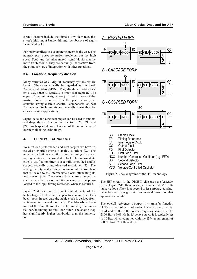
4. THE NEW TECHNOLOGY
To meet our performance and cost targets we have fo-cused on hybrid numeric + analog solutions [22]. The numeric part attenuates jitter from the timing reference, and generates an intermediate clock. The intermediate clock's justification jitter is spectrally smoothed and/or shaped, typically using advanced techniques [23]. The analog part typically has a continuous-time oscillator that is locked to the intermediate clock, attenuating its justification jitter. The various blocks are arranged in such a way that an output frame sync can be phase-locked to the input timing reference, when so required.
Figure 2 shows three different embodiments of the technology, all of which happen to contain dual feed-back loops. In each case the stable clock is derived from a free-running crystal oscillator. The black-box dyna-mics of the overall circuit are determined by the nume-ric loop, including the first loop filter. The analog loop has significantly higher bandwidth than the numeric loop.
A - NESTED FORM
C - COUPLED FORM
FD FLF NCOTR
SD SLF VCOIC
÷
÷
FD FLF NCOTR
SD SLF VCOIC
÷
÷
FD FLF NCOTR
SD SLF VCOIC
÷
B - CASCADE FORM
TR Timing Reference
FD First Detector FLF First Loop Filter NCO Number-Controlled Oscillator (e.g. FFD) SD Second Detector SLF Second Loop Filter VCO Voltage-Controlled Oscillator
IC Intermediate Clock OC Output Clock
SC Stable Clock
SC
OC
OC
OC
SC
SC
Figure 2 Block diagrams of the JET technology
The JET circuit in the DICE II chip uses the 'cascade form', Figure 2-B. Its numeric parts run at ~50 MHz. Its numeric loop filter is a second-order software-configu-rable bit -serial design, with an internal resolution that approaches 96 bits.
The overall reference-to-output jitter transfer function (JTF) is that of a third order lowpass filter, i.e. 60 dB/decade rolloff. Its corner frequency can be set to 2800 Hz to 0.09 Hz in 15 octave steps. It is typically set to 10 Hz, which complies with the 1394-requirement of -60 dB from 200 Hz and up.

Frandsen and Travis Clean Clocks, Once and for All?
AES 120th Convention, Paris, France, 2006 May 20–23
Page 7 of 21
Figure 3 Jitter Transfer Function of JET when the bandwidth is set to 10 Hz.
The jitter peaking, which is how much jitter is gained through the JET approx. one 3’rd of the corner frequen-cy is 1 dB. The AES3-1992 standard specifies jitter peaking of maximum 2 dB. This is specified to reduce the risk of jitter accumulution through a series of clock circuits.
From the unlocked state, a bandwidth ramping feature keeps the lock time low.
The justification jitter is given a highpass spectrum with second-order slope. This is synergistic with the fact that the analog loop lowpass-filters the jitter on the intermediate clock. It lets us keep the bandwidth of the analog loop above 100 kHz, which in turn lets us use a low Q oscillator. An ordinary on chip ring oscillator is used. The high loop bandwidth reflects the fact that a lot of feedback is being applied. The feedback suppresses interference from various paths, including the oscil-lator's supply rail. Provision is also made for an off-chip oscillator to be used.
To minimize fold down of the justification jitter, the phase detector in the analog loop is of a naturally linear type. Note also that it has more inputs than most phase detectors. This is apparent in Figure 2-B. This detector does phase comparisons at the clock rate, but also phase locks the frame syncs [24].
Our work on the various strands of this new clocking technology started in 1998, and led to patent applica-tions in 1999 and 2003 [22], [23], and [24] .
5. PERFORMANCE
5.1. General approach
The new technology has been implemented in the DICE II chip from TC Applied Technologies [1]. In order to investigate the performance level of the JET different approaches have been made. These include simple oscilloscope measurements [8] plus investigations made using an audio measurement tool by Audio Precision (S2C) [7] and phase noise analyzer by Aeroflex [9]. Refer to [14] and [2] for more info on appropriate jitter measurements.
The mentioned methods represent different ways of analysing the behaviour of the resulting clock of the technology. This would be the clock (24.576 MHz @ 48 kHz sampling rate) that in typical designs would be used as a sampling clock for ADC or DAC converters and as a reference for digital audio interfaces e.g. AES3 transmitters.
Focus has been directed towards intrinsic jitter of the different examined clock circuits. This means the resul-ting jitter in the clock circuit when being a clock master or when slaving to a very low jitter reference clock.
Measuring Jitter Transfer Function (the ability to sup-press jitter) and jitter tolerance (the ability to track in-coming jitter) goes beyond this paper but they have been thoroughly verified on JET through measurements to be as theory describes. Reference to theory in chapter 4 The new technology for more information.
All measurements are carried out at 48 kHz sampling rate.
Primary results are presented in this chapter. For the re-maining results we refer to the appendix.
This paper is not evaluating audibility of jitter – only measurable parameters are evaluated. For information on audibility we refer to [12] and [13].
5.1.1. The JET setup
This paper examines two different setups of the JET both implemented on the DICE II chip. One using the on-chip ring oscillator type VCO and one using an external LC-type VCO [16]. Due to the performance of the specific LC-type VCO, which is typically an order of magnitude better than the on-chip equivalent, the

Frandsen and Travis Clean Clocks, Once and for All?
AES 120th Convention, Paris, France, 2006 May 20–23
Page 8 of 21
bandwidth of the external analog JET loop is set to 50kHz where the on-chip loop is 200kHz. Refer to the appendix for a circuit diagram for driving the external VCO.
The two different bandwidths show compromises be-tween the JET NCO noise shaped jitter, the analog loop jitter transfer function (NCO jitter rejection) and the analog loop VCO self noise.
The reference clock for the numeric part of the JET is 50.0 MHz.
5.1.2. Comparisons
Performance of the JET is measured in both clock mas-ter mode and clock slave mode, slaving to the S2C without any jitter being applied.
For comparison the performance of a standard crystal oscillator module is measured. A crystal oscillator is commonly known as being the best performing clock master solution for any type of audio converter.
Further measurements are made on other clocking technologies including TC Electronic System 6000 [6], which is a dual stage Phase Locked Loop (PLL) solution, well known for excellent jitter performance in relation with ADCs and DACs. The internal 256Fs (12.288 MHz @ 48 kHz sampling rate) clock has been examined. Reference to [17] for more information.
Furthermore measurements for other well performing clocking technologies based on DDS (direct digital synthesis) are presented. External 256Fs (12.288 MHz @ 48 kHz sampling rate) clock output has been exa-mined on two products (product A and B). Both clock products feature extensive jitter rejection on the refe-rence clock input.
Finally measurements on a typical audio product are presented. The internal ADC 256Fs signal has been carefully buffered to reflect the ADC clock, brought out and examined.
5.1.3. Wideband jitter spectrum and bandpass filtered jitter
The PN8000 phase noise analyzer plus 2023A low phase noise signal generator from Aeroflex [9] features a method for measuring phase noise on stable clock sources like a crystal oscillator module or a locked PLL
circuit. This is done by tuning the signal generator to have the same frequency as the device under test (DUT) and then analyzing the resulting demodulated phase noise after an RF phase detector. This method offers an extremely low residual noise close to the carrier provi-ding a minimum FFT frequency of 0.01 Hz offset to the carrier. 10Hz offset to the carrier is chosen as the mini-mum FFT frequency is this paper.
The FFTs are presented as seconds/root(Hz) on the y-axis and frequency offset to the carrier on the x-axis.
The Aeroflex system is able to calculate the peak-peak and the RMS jitter in settable frequency bands from the FFT measurement.
A number for the full FFT band 10 Hz to 1 MHz is cal-culated, a 100 Hz to 40 kHz band has been chosen to calculate a baseband jitter number (suggested by [14]) and finally a 100 kHz to 1 MHz band has been chosen. The latter represents a frequency band in which PWM type DACs typically are sensitive to jitter.
5.1.4. DAC jitter susceptibility
Recall that jitter only affects audio quality when changing domain (D to A, A to D or D to D asynchro-nously). Any sampling clock jitter will modulate into the converted audio. Sampling jitter affects the slew rate of the audio signal which means that a full scale 20 kHz audio tone will be a good signal to use when examining the jitter level on the sampling clock. We examine the JET and System 6000 clock performance by feeding a high-end DAC with the regenerated clock from each technology. On a linear frequency axis jitter will show as symmetric skirts around the 20 kHz tone.
5.1.5. Jitter extracted from AES3 signal
The System 2 Cascade from Audio Precision [7] features ways to extract jitter transferred by an AES3 carrier signal. The measurement chosen for this paper extracts the jitter as the error signal in the digital input phase locked loop and presents a bandpass filtered number. There are different filters; in this paper 700 Hz to 100 kHz (s tandard AES3-1992 [18] interface filter) and 50 Hz to 100 kHz are chosen.
5.1.6. Long-term jitter (interval jitter)
Using an oscilloscope long-term jitter or interval jitter can be measured delaying the trigger and this way

Frandsen and Travis Clean Clocks, Once and for All?
AES 120th Convention, Paris, France, 2006 May 20–23
Page 9 of 21
capture the accumulated jitter within that interval. There are suggestions [14] using 1ms trigger delay and mea-sure the RMS jitter because this interval gives a loose approximation to the 100 Hz highpass response of wide-band jitter. This paper presents the interval jitter measured in peak-peak using two intervals (2 µs and 8 µs) – the oscilloscope used did not feature 1 ms trigger delay.
5.2. Measurement results
5.2.1. DAC jitter susceptibility on System 6000 and JET
-150
+0
-140
-130
-120
-110
-100
-90
-80
-70
-60
-50
-40
-30
-20
-10
dBr A
0 24k2k 4k 6k 8k 10k 12k 14k 16k 18k 20k 22k
Hz
Figure 4 System 6000 DAC, in clock master mode (lower trace) and in clock slave mode (upper trace). No
jitter was applied on reference clock.
-150
+0
-140
-130
-120
-110
-100
-90
-80
-70
-60
-50
-40
-30
-20
-10
dBr A
0 24k2k 4k 6k 8k 10k 12k 14k 16k 18k 20k 22k
Hz
Figure 5 JET with on-chip VCO and DAC, in clock slave mode. No jitter was applied on refe rence clock.
A 20 kHz tone has been DA-converted on both System 6000 and a JET/DAC setup. Audio Precision FFT de-tails are: 65536 Hz sample rate, 32k points, bin width 1 Hz, equiripple window, 32 averages, plotted in 1023 steps (23Hz stepsize), 0 to 24 kHz.
The sidebands on the JET/DAC 20 kHz tone are lower than on System 6000 in clock slave mode (upper trace in Figure 4). There are spikes at maximum -134 dB below the 20 kHz on the JET/DAC and on System 6000 in clock slave mode the sampling jitter forms skirts starting at -130 dB below the 20 kHz and ending in the noise floor at 2 kHz offset from the 20 kHz.
In general the jitter modulation effect on the JET/DAC is low and compares well to a dual PLL solution as on System 6000.
There is a difference on System 6000 from clock master mode to clock slave mode. This is due to the fact that System 6000 is clocked directly from a crystal oscillator in master mode and though a costly dual PLL design (which reduces incoming interface jitter to a high extent, see [17]) in clock slave mode.
5.2.2. Jitter spectral density plots on System 6000 and JET
Figure 6 Jitter spectral density. System 6000 in clock slave mode. No jitter was applied on reference clock.
Aeroflex FFT details are: 400 points/decade, Hanning window, 10 averages, 10 Hz to 1 MHz.
Figure 6 and Figure 7 shows the jitter spectral density of System 6000 and JET (with on-chip VCO). Note the difference on the two plots concerning the y-axis scale.
baseband jitter (100Hz to 40kHz) = 55 ps RMS bandpass jitter (10Hz to 1MHz)= 106 ps RMS

Frandsen and Travis Clean Clocks, Once and for All?
AES 120th Convention, Paris, France, 2006 May 20–23
Page 10 of 21
Figure 7 Jitter spectral density. JET with on-chip VCO in clock slave mode. No jitter was applied on reference
clock.
From 3 kHz and down the JET has lower jitter spectral density (the noise part) than the System 6000. This compares well with the observations on DAC measurements in Figure 4 and Figure 5. The jitter spec-tral density tendency can be confirmed in Table 1 where summed RMS values of the different bands can be compared. In the baseband (100 Hz to 40 kHz) JET and System 6000 are close to the same level. The reason for this is that the spurs on JET are a bit higher than on System 6000.
Comparing the “PWM” band (100 kHz to 1MHz) both on the jitter density figures and in the table JET shows higher level than System 6000. This is due to the cost efficient on-chip VCO, which is noisier than its external LC-type equivalent. This is not proven to have any effects on audio quality on common converters.
Because the bin width of the DAC plots is 1 Hz the jitter level readings in the DAC plots can be compared to the jitter spectral density plots. Sampling jitter will modula-te an audio tone and produce side bands according to this formula [13], [12]:
Side band level = -107 + 20log(F) + 20log(J) dBr, for sine wave signals at F kHz with J ns RMS of clock jitter.
The sidebands on the JET/DAC FFT plot Figure 5 reads at 150Hz offset to -134 dBr. This level calculates to 2.2 ps RMS. A corresponding reading can be done on the jitter spectral density plot Figure 7 where a spur at 100 Hz reads to 3 ps RMS.
System 6000 jitter density plot Figure 6 reads at 500 Hz to 2 ps RMS. This level would create 500 Hz sidebands to the 20 kHz tone at -135 dBr. The corresponding rea-ding from the DAC plot Figure 4 at 500 Hz offset to the 20 kHz reads -133 dBr.
A factor to include would be the window scaling factor, which is 4.2 dB for an equiripple window [2]. The use of this window lifts the noise part of the DAC FFT plots and should be compensated for in the readings from the System 6000 plot because these readings are done on the noise part of the plot. This means that the -133 dBr reading would be -137 dBr instead.
Spur often appears on the jitter spectral density plots. It can be hard to locate the source of these discrete frequency spikes similar to the detective work needed for cleaning the noise floor of an audio converter for spikes. The sources of both types of spikes can be the same e.g. noise in power rails or beating clocks or switching circuitry.
Figure 8 Jitter spectral density. Typical audio product, clock slave mode. No jitter was applied on reference
clock.
baseband jitter (100Hz to 40kHz) = 42 ps RMS bandpass jitter (10Hz to 1MHz)= 152 ps RMS
baseband jitter (100Hz to 40kHz) = 4300 ps RMS bandpass jitter (10Hz to 1MHz)= 4300 ps RMS
Frandsen and Travis Clean Clocks, Once and for All?
AES 120th Convention, Paris, France, 2006 May 20–23
Page 11 of 21
Audio Precision Aeroflex LeCroy
700Hz-100kHz
50Hz-100kHz
Full band 10Hz-1MHz
Baseband 100Hz-40kHz
”PWM” band 100kHz-1MHz 2µs 8µs
Clock ref. peak Peak ps RMS ps p-p ps RMS ps p-p ps RMS ps p-p p-p p-p
Master 1ns 1.5ns 184 880 25 132 175 830 1ns 1.6ns On-chip VCO
Slave 1ns 1.5ns 152 754 42 194 116 619 1ns 1.6ns
Master 800ps 1.5ns 27 143 23 120 5 26 150ps 200ps
JET
External LC-type VCO Slave 800ps 1.5ns 89 339 26 140 69 227 300ps 350ps
Master 500ps 600ps 25 133 5 24 10 43 150ps 200ps TC System 6000
Slave 500ps 600ps 106 530 55 328 39 135 200ps 300ps
Crystal oscillator Master NA NA 79 298 0.5 3 1 4 100ps 100ps
Master 560ps 1ns 150 640 78 324 77 273 400ps 600ps Clock product A
Slave 560ps 1.2ns 325 1700 63 269 76 270 400ps 600ps
Master 800ps 1ns 82 460 4 22 26 124 400ps 400ps Clock product B
Slave 800ps 2ns 628 3200 119 715 23 116 500ps 500ps
Master 1.1ns 3.6ns 1800 7900 1800 7900 10 63 NA NA Typical audio product
Slave 2ns 5.2ns 4300 22000 4300 22000 11 65 NA NA
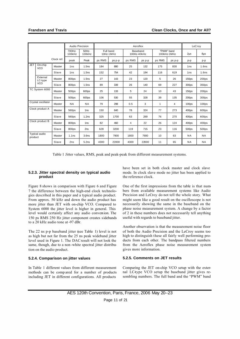
Table 1 Jitter values, RMS, peak and peak-peak from different measurement systems.
5.2.3. Jitter spectral density on typical audio product
Figure 8 shows in comparison with Figure 6 and Figure 7 the difference between the high-end clock technolo-gies described in this paper and a typical audio product. From approx. 50 kHz and down the audio product has more jitter than JET with on-chip VCO. Compared to System 6000 the jitter level is higher in general. This level would certainly affect any audio conversion. The 150 ps RMS 250 Hz jitter component creates sidebands to a 20 kHz audio tone at -97 dBr.
The 22 ns p-p baseband jitter (see Table 1) level is not as high but not far from the 25 ns peak wideband jitter level used in Figure 1. The DAC result will not look the same, though, due to a non -white spectral jitter distribu-tion on the audio product.
5.2.4. Comparison on jitter values
In Table 1 different values from different measurement methods can be comp ared for a number of products including JET in different configurations. All products
have been set in both clock master and clock slave mode. In clock slave mode no jitter has been applied to the reference clock.
One of the first impressions from the table is that num-bers from available measurement systems like Audio Precision and LeCroy do not tell the whole story. What might seem like a good result on the oscilloscope is not necessarily showing the same in the baseband on the phase noise measurement system. A change by a factor of 2 in these numbers does not necessarily tell anything useful with regards to baseband jitter.
Another observation is that the measurement noise floor of both the Audio Precision and the LeCroy seems too high to distinguish these all fairly well performing pro-ducts from each other. The bandpass filtered numbers from the Aeroflex phase noise measurement system gives more information.
5.2.5. Comments on JET results
Comparing the JET on-chip VCO setup with the exter-nal LC-type VCO setup the baseband jitter gives re-sembling numbers. The full band and the “PWM” band
Frandsen and Travis Clean Clocks, Once and for All?
AES 120th Convention, Paris, France, 2006 May 20–23
Page 12 of 21
are approx. half the size with the external LC-type VCO. This indicates that the LC-type VCO could be used with benefit when clocking a PWM type DAC because this DAC type is known to be sensitive to jitter in that frequency band due to a full scale carrier often placed at 384 kHz [14], [15].
Note that the “PWM” jitter band does affect normal DACs also due to the signal aliases typically located around 8 times Fs e.g. 384 kHz. When DA-converting a 20 kHz tone aliases at 384 kHz +/ - 20 kHz will often be present at approx. 30 dB below the 20kHz tone. This is due to the digital regeneration filter in the DAC and any jitter (spurs and noise) located in the 384 kHz area would be modulated down into the audio band via the aliases and create complex jitter products in the audio band.
The aliases are often as sensitive to jitter as the 20kHz tone due to the frequency being the same factor higher than 20kHz as it is reduced in level (jitter affects the audio signal slew rate, equally affecting frequency and level). But because typical crystals and VCXO based PLLs often have little jitter in the “PWM” band, jitter modulated down into the audio band from this higher band is typically not dominant. When using clocking technologies that generate more jitter in the “PWM” band the jitter modulation products from the 8Fs aliases can become significant in the audio band.
Basically there is no difference in the setup when run-ning JET as a clock master or as a clock slave. In both cases the numeric loop is locked to a reference clock (either an external clock or a clock divided down from a local crystal oscillator) and via the analog loop is gene-rating the resulting clocks. Comparing the JET with external LC-type VCO in clock master mode and clock slave mode indicates a difference especially in the “PWM” band, which can be confirmed by studying the jitter spectral density plot in the appendix. Spurs seem to be the difference but the authors did not locate the source of this.
Comparing clock slave results of the baseband jitter of the JET (both on-chip and external VCO) to System 6000 it is clear that JET has even better performance. Using the System 6000 as a reference for user’s satis-faction on high quality converter performance supports that JET is well performing. In the “PWM” band the System 6000 performs better than JET.
5.2.6. Other observations
We refer to the appendix for jitter spectral density plots for the remaining products in Table 1.
Note the spectrum of a crystal oscillator, which is com-monly accepted as the least jittery clock source. Results in Table 1 seem to underline this. System 6000 in clock master mode is using a crystal oscillator module. By comparing the crystal and System 6000 in clock master mode difference in this technology alone can be ob-served. System 6000 has approx. 10 times higher RMS jitter in “PWM” band and in the baseband.
Comparing JET to the two clock products it is clear that JET does well. In both full band and baseband the JET performs better than the two clock products. Only in the “PWM” band one of the products is performing better than JET. One of them has a fairly large jitter amount in the baseband. According to the Audio Precision mea-surement this jitter is located below 700Hz and the jitter spectral density plot confirms this - 2 “bumps” located at 100Hz and 5 0Hz.
It will be fair to claim that the DAC measurement and the Aeroflex measurement are what we gain most information from in this paper. The simpler jitter num-bers measured with the oscilloscope and via the extrac-ted jitter from an AES3 carrier signal are vague descrip-tions of the resulting sampling jitter audio consequence of any of the investigated products.
In this chapter a number of clocking technologies have been investigated. All technologies would normally be referred to as well performing except the tested audio product. The JET compares well with the other techno-logies with regards to intrinsic jitter and receives further credit by offering wide locking range and its excep-tionally high ability to suppress jitter at a much lower cost. By referring to chapter 2 Design requirements we can see that the JET actually meets the target values we set on baseband and wideband jitter.
6. FEATURES
The main features of the JET are extensive jitter reduction, extremely low intrinsic jitter, wide frequency range, fast lock time, and low cost. The use of numeric techniques enables several additional features to be in-cluded at low marginal cost.

Frandsen and Travis Clean Clocks, Once and for All?
AES 120th Convention, Paris, France, 2006 May 20–23
Page 13 of 21
These features include
• Flexible master clock rate generation
• Flexible locking
• Ability to freeze the current rate
• Clock and sync analysing tools
6.1. Flexible master clock rate generation
Registers in JET can be set to generate internal master clock rates with frequency resolution and precision that in many cases will comply with standards like AES11-2003 (grade 1 clock precision = +/- 1 PPM ) [10]. A 49.152 MHz is used as the JET reference crystal os-cillator in Table 2. For the output rates shown, the ratio locking imposes no additional deviation on the frequency error of this reference crystal. For a design with strong needs for a low sampling rate deviation a reference oscillator with low deviation should be used.
Output base rate
Hz Comment Deviation
PPM
44100 Std. audio rate 0
44144.1 44.1k x 1001/1000 0 44055.9… 44.1k x 1000/1001 0 45937.5 44.1k x 25/24 0 42336 44.1k x 24/25 0 48000 Std. audio rate 0 48048 48k x 1001/1000 0
47952.04… 48k x 1000/1001 0 50000 48k x 25/24 0
46080 48k x 24/25 0
Table 2 Example of different sampling rates generated from a 49.152 MHz crystal reference.
6.2. Flexible locking
The JET design is able to lock to very low frequencies and create phase locked standard audio rates. E.g. locking to 25 Hz while generating a phase locked base rate at 48k kHz and a 512xBase Rate at 24.567 MHz. All of the rates in Table 2 can be generated while locking to a 48k AES3/wordclock, 1394 Cycle Time, video 27 MHz, MPEG 90 kHz, and common off-air frequency references . Other known reference signals include 256x "superclock" and video "color-black".
6.3. Ability to freeze the current rate
JET features ability to freeze the actual current sampling rate. It can be done both manually and automatically if the input clock reference is lost on e.g. an AES 3, ADAT or a wordclock input. When the reference input clock is reestablished the JET can smoothly regain lock.
This feature is useful in a number of situations e.g. a broadcast installation where the reference for one of the audio processing products is lost. If this product freezes the actual rate prior to the reference loss the down stream products might not get disturbed by this incident.
Another example could be a computer IO product which is in clock slave mode to a 48 kHz digital input. If the reference input fails the IO product might switch to a different sampling rate (e.g. default 44.1 kHz) instan-taneously and bring the computer audio host application (e.g. a music sequencer) into a failing state. If the IO product froze the actual 48 kHz when the reference was lost the host application would still be running.
In general bigger systems with critical live demands (broad cast, PA etc.) will potentially benefit greatly from this feature.
6.4. Clock and sync analysing tools – pinpointing errors
Few audio processing products analyse the digital audio inputs other than verifying the sampling rate. The JET features counters from which sampling rate can be cal-culated including statistics. The DICE II chip, which include the first implementation of JET further offers phase offset calculation on the different digital inputs on the chip. The user will potentially benefit greatly from this by being able to pinpoint which digital interface is the failing one.
A number of potential digital interface deficiencies are described [4]. If the user could monitor all interfaces in an audio network system based on different interface types e.g. AES, ADAT, 1394 etc. then the general sys-tem fault tolerance could be raised because the user would be able to locate and replace the failing products.
The increasing availability of such features hopefully will affect operational practice like in the example above.

Frandsen and Travis Clean Clocks, Once and for All?
AES 120th Convention, Paris, France, 2006 May 20–23
Page 14 of 21
7. IMPLICATIONS
Having presented a new clocking technology that features low-cost high-performance clock cleaning it is of interest to discuss if this is likely to affect clock dis-tribution scheme practices at the system level.
Often digital audio systems uses a master clock distributor scheme which sends the house clock to all products that can receive it. This master clock product may reference to an outside clock source and reduce jitter on this clock before distributing it.
Reasons for this may be that well performing jitter rejection circuits are expensive and therefore mainly placed in one central place. Another reason for having a central clock is that the clock distribution is fixed and easily handled because it is independent of the signal routing.
But jitter is important in relation with domain shifts (ADC, DAC and ASRC). This is where any jitter in the sampling clock will be modulated into the audio and knowing that jitter may be induced across cables and added in poorly designed clock circuits then centrally clock cleaning may not be the best solution.
Local clock cleaning in every product in a digital system or every domain shifting product in a system could be the alternative solution and for that to be an option it has to be cost efficient and well performing. It will make the converters in the system fairly indepen-dent of the potential jit ter sources.
The benefits apply equally for network based system e.g. 1394 and for point-to-point links such as AES3/SPDIF and ADAT.
In broadcast audio/video systems it is commonly accepted that using AES11 (AES3 with no audio) as a reference signal carrier is less robust than its square-wave wordclock equivalent. A reason for this is that the bi-phase coding characteristic in AES11 enables jitter build up across long cable distances. Therefore this signal is often replaced by the simpler wordclock sig-nal. The problem is that the wordclock signal carries less timing information than AES11 e.g. not the X/Y/Z preambles, which gives information on audio relation to picture. Fixed and controlled relation between audio and picture is of big interest in broadcast in these installa-tions.
If local clock cleaning was implemented in all broad-cast products the AES11 signal would probably be accepted as the standard timing reference signal. This way the audio relation to picture would be controlled better.
8. CONCLUSION
In conclusion, we have presented JET (Jitter “Elimi-nation” Technology) as a new clock regeneration solu-tion, which combines extensive jitter rejection, low in-trinsic jitter, wide frequency range, fast lock time and low cost. JET has been implemented on the DICE II chip by TC Applied Technologies.
We have found a specification set for the ideal clock regeneration circuit through user requirements and pro-duct designer requirements. The following specific pa-rameters have been included: Ability to suppress jitter, intrinsic jitter, frequency locking range, lock time, and cost.
While touching on alternative approaches like dual PLL and DDS (Direct Digital Synthesis) solutions the theory of the JET has been presented.
The performance level of the JET has been investigated through different approaches. These include simple oscilloscope measurements plus investigations made using an Audio Precision measurement tool and a high performance phase noise analyzer from Aeroflex.
The use of numeric techniques in JET enables several additional features to be included in the technology at low marginal cost. This include: Flexible master clock rate generation, flexible locking, ability to freeze the current rate, and clock and sync analysing tools.
Having presented a new clocking technology that fea-tures low-cost high-performance clock cleaning it is likely to affect clock distribution practices at the system level. Local clock cleaning in every product in a digital system could be the alternative solution to a central clock cleaning (master clock product, house clock). It will make all the domain converters in the system inde-pendent of the potential jitter sources.
9. ACKNOWLEDGEMENTS
The authors wish to thank Guillaume De Giovanni, Di-rector of Business Development Phase noise, Aeroflex

Frandsen and Travis Clean Clocks, Once and for All?
AES 120th Convention, Paris, France, 2006 May 20–23
Page 15 of 21
France and Tonni Brammer, Sales manager, Aeroflex Denmark for support during the measurement period of this paper.
The authors also wish to thank Morten Lave, CEO / Managing Director, TC Applied Technologies and Kim Rishoej, CTO, TC Group for assistance and corrections to the paper.
10. REFERENCES
[1] DICE II chip from TC Applied Technologies www.tctechnologies.tc and distributed by Wave-front semiconductor www.wavefrontsemi.com. The chip features multiple audio interface types: AES3, ADAT, TDIF, ADC and DAC ports. Additionally JET high-order jitter rejection and IEEE1394B IEC 61883-6 audio streaming is featured.
[2] Audio Precision, Application note #5: Measure-ment Techniques for Digital Audio by Julian Dunn. Associated AP measurement files. Available at www.ap.com.
[3] Julian Dunn, IEEE 1394 and sampling jitter, presented at AES UK Conference: Moving Audio - Pro-Audio Networking and Transfer, 2000 April .
[4] Christian G. Frandsen, Morten Lave, Plug and Play? An investigation into problems and solutions of digital audio networks, presented at AES116th Convention, Berlin, Germany, 2005 May 8-11.
[5] Soren Nielsen & Thomas Lund, Overload in Signal Conversion, presented at AES 23rd International Conference, Copenhagen, Denmark, 2003 May 23-25.
[6] TC Electronic, System 6000, high end audio pro-cessor, www.tcelectronic.com.
[7] Audio Precision, System 2 Cascade, dual domain audio measurement tool, www.ap.com.
[8] LeCroy, LT364L, oscilloscope, www.lecroy.com.
[9] Aeroflex, PN8000, phase noise analyser + 2023A signal generator, www.aeroflex.com.
[10] AES11-2003, AES recommended practice for digi-tal audio engineering – Synchronization of digital audio equipment in studio operations.
[11] IEC 61883-6 Ed. 2: Consumer audio/video equipment – Digital interface – Part 6: Audio and music data transmission (TA4).
[12] Julian Dunn, Jitter and Digital Audio Performance Measurements, presented at AES UK Conference: Managing the Bit Budget, 1994 April.
[13] Eric Benjamin and Benjamin Gannon, Theoretical and Audible Effects of Jitter on Digital Audio Quality, presented at the AES105th Convention, San Francisco California, 1998 September 26-29.
[14] Chris Travis, Paul Lesso, Specifying the Jitter Performance of Audio Components, presented at the AES117th Convention, San Fransico, CA, USA, 2004 October 28-31.
[15] Bruno Putzeys and Renaud de Saint Moulin, Effects of Jitter on AD/DA conversion. Speci-fication of Clock Jitter Performance, presented at the AES116th Convention, Berlin, Germany, 2004 May 8–11.
[16] Mini Circuits, LC-type VCO, POS -50, www.minicircuits.com
[17] Christian G. Frandsen, Clock and Synchronization in System 6000, a whitepaper on available on www.tcelectronic.com
[18] AES3-1992 (r1997) incl. amendment 1-4, AES re-commended practice for digital audio engineering – Serial transmission format for two -channel linear-ly represented digital audio data.
[19] US patent 1996 000635234, "Digital audio re-solving apparatus and method", Avid Technologies, Inc., US, Jeffrey C. Mock.
[20] US patent 1989 000439662, "Frequency synthesi-zers having dividing ratio controlled by sigma -delta modulator", Carleton University, Canada, Thomas A. D. Riley.
[21] US patent 1998 5825253, "Phase-locked loop with noise shaper", Qualcomm, Inc., US, Lennart Karl-Axel Mathe and Saed G. Younis.

Frandsen and Travis Clean Clocks, Once and for All?
AES 120th Convention, Paris, France, 2006 May 20–23
Page 16 of 21
[22] "Hybrid numeric-analog clock synchronizer". Part one of international patent application WO 2004/088845, "Method of establishing an oscillator clock signal". Chris Travis.
[23] "High-performance number-controlled oscillator". Part two of international patent application WO 2004/088845, "Method of establishing an oscillator clock signal". Chris Travis.
[24] "Clock-and-frame asynchrony detector". Part three of international patent application WO 2004/088845, "Method of establishing an oscillator clock signal". Chris Travis.

Frandsen and Travis Clean Clocks, Once and for All?
AES 120th Convention, Paris, France, 2006 May 20–23
Page 17 of 21
11. APPENDIX
Jitter spectral density. JET on-chip VCO, clock master mode, carrier 24.576 MHz.
Jitter spectral density. JET on-chip VCO, clock slave mode, carrier 24.576 MHz. Same as Figure 7. No jitter was applied on reference clock.
Jitter spectral density. JET external LC-type VCO, clock master mode, carrier 24.576 MHz.
Jitter spectral density. JET external LC-type VCO, clock slave mode, carrier 24.576 MHz. No jitter was applied on reference clock.
baseband jitter (100Hz to 40kHz) = 25 ps RMS bandpass jitter (10Hz to 1MHz)= 184 ps RMS
baseband jitter (100Hz to 40kHz) = 23 ps RMS bandpass jitter (10Hz to 1MHz)= 27 ps RMS
baseband jitter (100Hz to 40kHz) = 26 ps RMS bandpass jitter (10Hz to 1MHz)= 89 ps RMS
baseband jitter (100Hz to 40kHz) = 42 ps RMS bandpass jitter (10Hz to 1MHz)= 152 ps RMS

Frandsen and Travis Clean Clocks, Once and for All?
AES 120th Convention, Paris, France, 2006 May 20–23
Page 18 of 21
Jitter spectral density. TC Electronic System 6000, clock master mode, carrier 12.228 MHz.
Jitter spectral density. TC Electronic System 6000, clock slave mode, carrier 12.228 MHz. Same as Figure 6. No jitter was applied on reference clock.
Jitter spectral density. Crystal oscillator module, carrier 49.152 MHz.
Jitter spectral density. Clock product A, DDS design, clock master mode, carrier 12.228 MHz.
baseband jitter (100Hz to 40kHz) = 5 ps RMS bandpass jitter (10Hz to 1MHz)= 25 ps RMS
baseband jitter (100Hz to 40kHz) = 0.5 ps RMS bandpass jitter (10Hz to 1MHz)= 78 ps RMS
baseband jitter (100Hz to 40kHz) = 78 ps RMS bandpass jitter (10Hz to 1MHz)= 150 ps RMS
baseband jitter (100Hz to 40kHz) = 55 ps RMS bandpass jitter (10Hz to 1MHz)= 106 ps RMS

Frandsen and Travis Clean Clocks, Once and for All?
AES 120th Convention, Paris, France, 2006 May 20–23
Page 19 of 21
Jitter spectral density. Clock product A, DDS design, clock slave mode, carrier 12.228 MHz. No jitter was applied on reference clock.
Jitter spectral density. Clock product B, DDS design, clock master mode, carrier 12.228 MHz.
Jitter spectral density. Clock product B, DDS design, clock slave mode, carrier 12.228 MHz. No jitter was applied on reference clock.
Jitter spectral density. Typical audio product, clock master mode, carrier 12.228 MHz.
baseband jitter (100Hz to 40kHz) = 63 ps RMS bandpass jitter (10Hz to 1MHz)= 325 ps RMS
baseband jitter (100Hz to 40kHz) = 119 ps RMS bandpass jitter (10Hz to 1MHz)= 628 ps RMS
baseband jitter (100Hz-40kHz) = 4300 ps RMS bandpass jitter (10Hz to 1MHz)= 4300 ps RMS
baseband jitter (100Hz to 40kHz) = 1800 ps RMS bandpass jitter (10Hz to 1MHz)= 1800 ps RMS
baseband jitter (100Hz to 40kHz) = 4 ps RMS bandpass jitter (10Hz to 1MHz)= 82 ps RMS

Frandsen and Travis Clean Clocks, Once and for All?
AES 120th Convention, Paris, France, 2006 May 20–23
Page 20 of 21
Jitter spectral density. Typical audio product, clock slave mode, carrier 12.228 MHz. No jitter was applied on reference clock. Same as Figure 8.
Circuit for driving the external LC-type VCO for JET.
baseband jitter (100Hz to 40kHz) = 4300 ps RMS bandpass jitter (10Hz to 1MHz)= 4300 ps RMS

Frandsen and Travis Clean Clocks, Once and for All?
AES 120th Convention, Paris, France, 2006 May 20–23
Page 21 of 21
-150
+0
-140
-130
-120
-110
-100
-90
-80
-70
-60
-50
-40
-30
-20
-10
dBr A
0 24k2k 4k 6k 8k 10k 12k 14k 16k 18k 20k 22k
Hz
Audio Precision, Jitter susceptibility, sampling jitter using a DAC. JET and DAC, in clock slave mode. No jitter was applied on reference clock. Same as Figure 5.
-150
+0
-140
-130
-120
-110
-100
-90
-80
-70
-60
-50
-40
-30
-20
-10
dBr A
0 24k2k 4k 6k 8k 10k 12k 14k 16k 18k 20k 22k
Hz
Audio Precision, Jitter susceptibility, sampling jitter using a DAC. S6k and DAC in clock master mode (lower trace) and in clock slave mode (upper trace). No jitter was applied on reference clock. Same as Figure 4.