advantages of using cmos - the henry samueli school of...
TRANSCRIPT
EECS 270C / Winter 2014 Prof. M. Green / U.C. Irvine 1
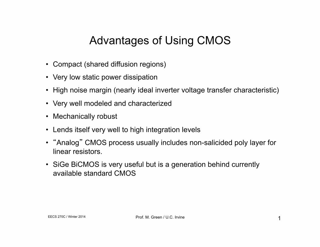
Advantages of Using CMOS
• Compact (shared diffusion regions)
• Very low static power dissipation
• High noise margin (nearly ideal inverter voltage transfer characteristic)
• Very well modeled and characterized
• Mechanically robust
• Lends itself very well to high integration levels
• “Analog” CMOS process usually includes non-salicided poly layer for linear resistors.
• SiGe BiCMOS is very useful but is a generation behind currently available standard CMOS
EECS 270C / Winter 2014 Prof. M. Green / U.C. Irvine 2
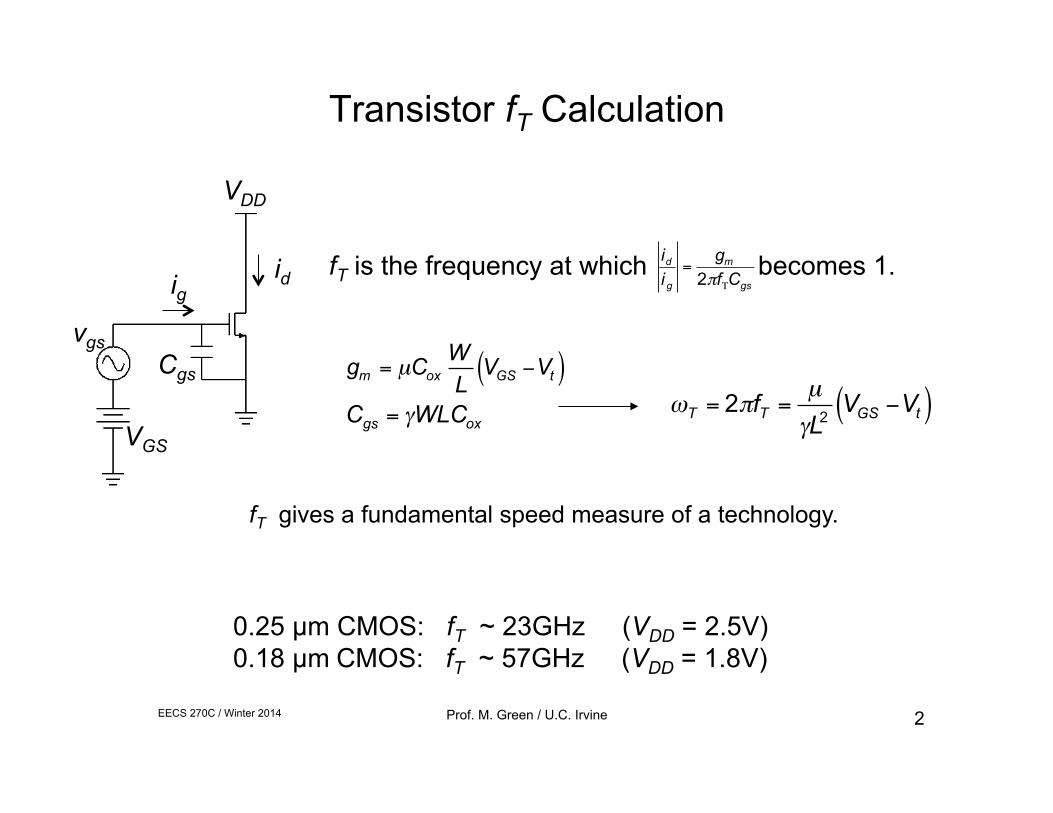
fT is the frequency at which becomes 1.
€
idi g
=gm
2πfΤCgs
€
gm = µCoxWL
VGS −Vt( )
€
Cgs = γWLCox
fT gives a fundamental speed measure of a technology.
0.25 µm CMOS: fT ~ 23GHz (VDD = 2.5V) 0.18 µm CMOS: fT ~ 57GHz (VDD = 1.8V)
€
ωT = 2πfT =µ
γL2VGS −Vt( )
VDD
Cgs
VGS
vgs
ig id
Transistor fT Calculation
EECS 270C / Winter 2014 Prof. M. Green / U.C. Irvine 3
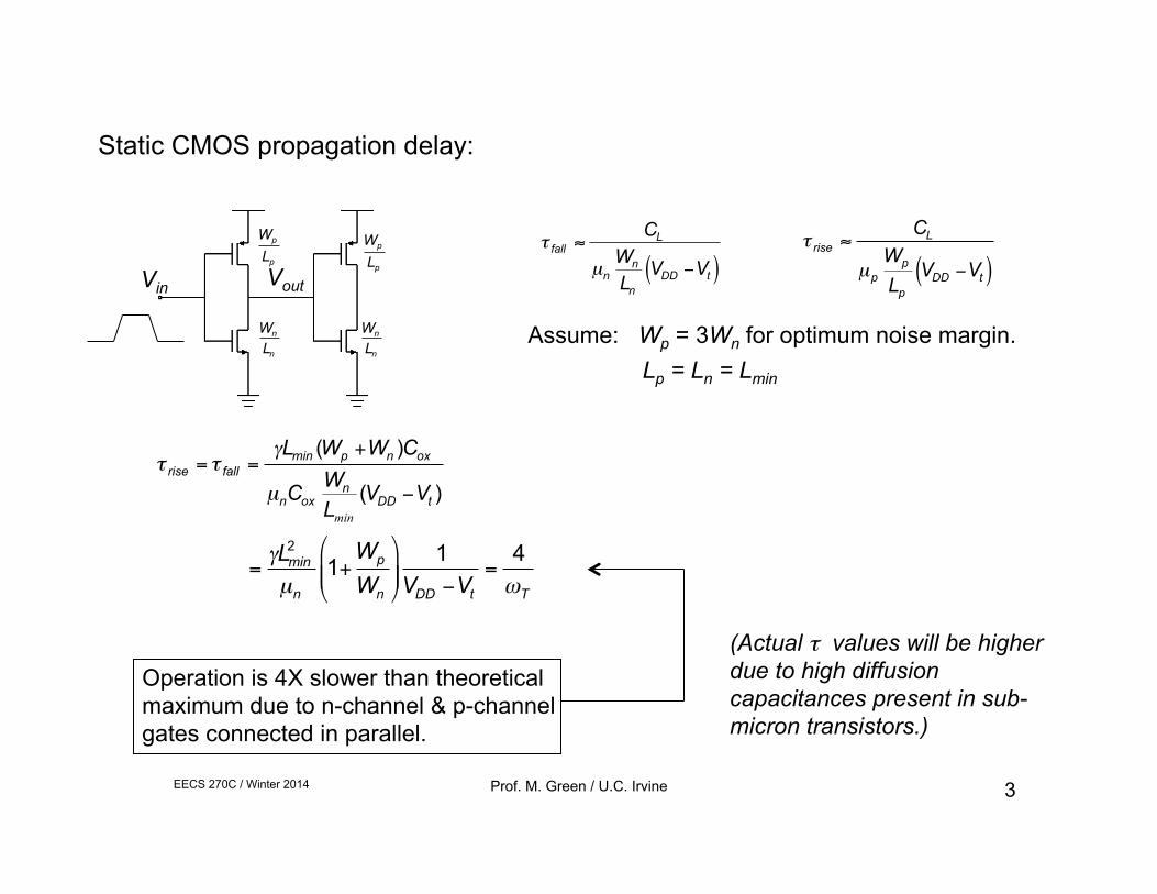
Static CMOS propagation delay:
€
τ fall ≈CL
µnWn
Ln
VDD −Vt( )
€
τ rise ≈CL
µpWp
Lp
VDD −Vt( )
Assume: Wp = 3Wn for optimum noise margin. Lp = Ln = Lmin
€
τ rise = τ fall =γLmin (Wp +Wn )Cox
µnCoxWn
Lmin
(VDD −Vt )
€
=γLmin
2
µn
1+Wp
Wn
#
$ % %
&
' ( (
1VDD −Vt
=4ωT
Operation is 4X slower than theoretical maximum due to n-channel & p-channel gates connected in parallel.
(Actual τ values will be higher due to high diffusion capacitances present in sub-micron transistors.)
Vin Vout
€
Wn
Ln
€
Wn
Ln
€
Wp
Lp
€
Wp
Lp
EECS 270C / Winter 2014 Prof. M. Green / U.C. Irvine 4
IG
ID
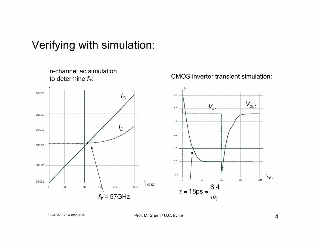
fT = 57GHz
Vout Vin
€
τ = 18ps ≈ 6.4ωT
n-channel ac simulation to determine fT: CMOS inverter transient simulation:
Verifying with simulation:
EECS 270C / Winter 2014 Prof. M. Green / U.C. Irvine 5
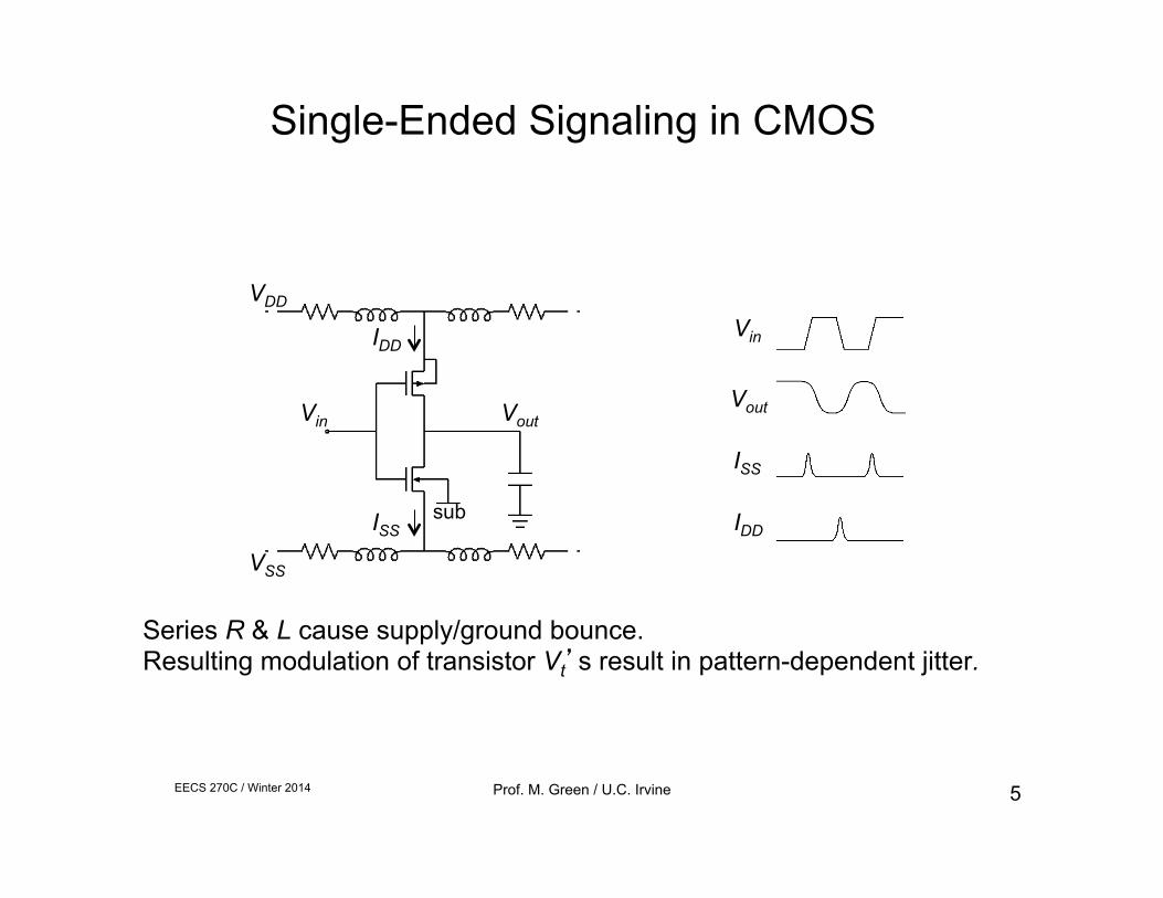
Single-Ended Signaling in CMOS
Series R & L cause supply/ground bounce. Resulting modulation of transistor Vt’s result in pattern-dependent jitter.
Vin Vout
sub
IDD
ISS
VDD
VSS
Vin
Vout
ISS
IDD
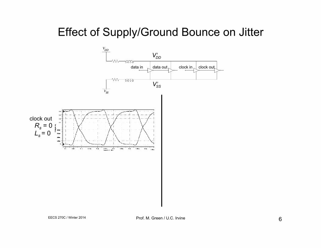
EECS 270C / Winter 2014 Prof. M. Green / U.C. Irvine 6
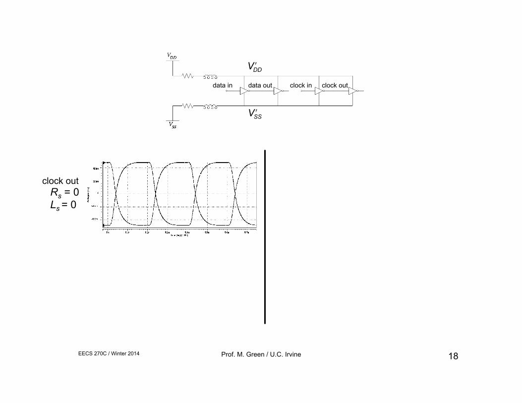
Rs = 0 Ls = 0
clock out
Rs = 5Ω Ls = 5nH
clock out
data in clock in clock out data out
€
" V DD
€
" V SS
€
" V DD
€
" V SS
data out
Rs = 5Ω Ls = 5nH
Effect of Supply/Ground Bounce on Jitter
EECS 270C / Winter 2014 Prof. M. Green / U.C. Irvine 7
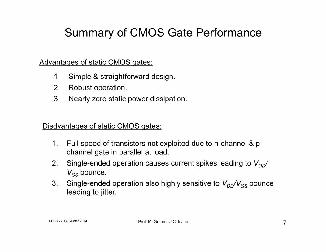
Summary of CMOS Gate Performance
1. Simple & straightforward design. 2. Robust operation. 3. Nearly zero static power dissipation.
Advantages of static CMOS gates:
1. Full speed of transistors not exploited due to n-channel & p-channel gate in parallel at load.
2. Single-ended operation causes current spikes leading to VDD/VSS bounce.
3. Single-ended operation also highly sensitive to VDD/VSS bounce leading to jitter.
Disdvantages of static CMOS gates:
EECS 270C / Winter 2014 Prof. M. Green / U.C. Irvine 8
Current-Mode Logic (CML)
• Based on conventional differential pair
• Differential operation
• Inherent common-mode rejection
• Very robust in the presence of common- mode disturbances (e.g., VDD / VSS bounce)
CML inverter: VDD
Vin+ Vin-
Vout- Vout+
ISS
R R
CL CL
EECS 270C / Winter 2014 Prof. M. Green / U.C. Irvine 9
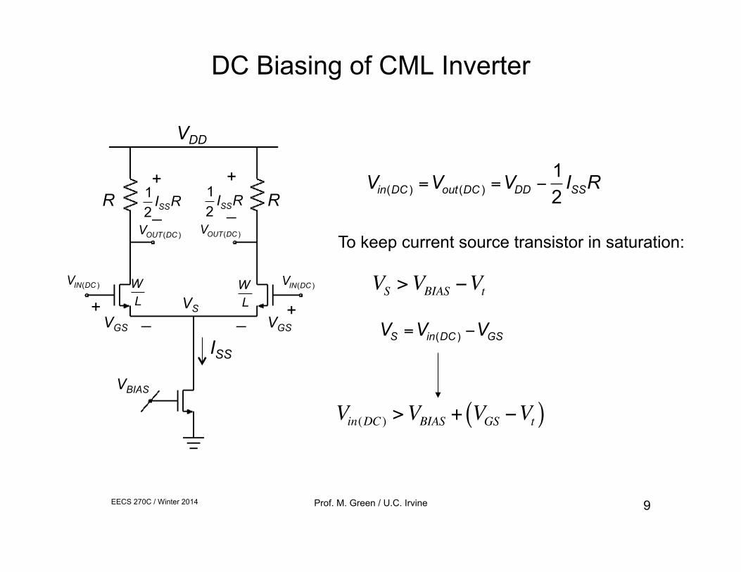
€
Vin(DC ) =Vout (DC ) =VDD −12
ISSR
To keep current source transistor in saturation:
VS >VBIAS −Vt
€
VS =Vin(DC ) −VGS
Vin(DC ) >VBIAS + VGS −Vt( )
€
12
ISSR+
_
€
12
ISSR+
_
VDD
R R
€
WL
€
WL
ISS
€
VIN(DC )
€
VOUT(DC )
€
VOUT(DC )
VS VGS
+ _ VGS
+ _
VBIAS
DC Biasing of CML Inverter
€
VIN(DC )
EECS 270C / Winter 2014 Prof. M. Green / U.C. Irvine 10
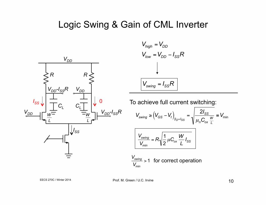
€
Vhigh =VDD
Vlow =VDD − ISSR
€
Vswing = ISSR
To achieve full current switching:
€
Vswing ≥ VGS −Vt( )|ID=ISS
=2ISS
µnCoxWL
≡Vmin
€
Vswing
Vmin
> 1 for correct operation
€
Vswing
Vmin
= R 12
µCoxWL
ISS
Logic Swing & Gain of CML Inverter
VDD
VDD VDD-ISSR
ISS
R R
CL CL
€
WL
€
WL
VDD-ISSR VDD
ISS 0
EECS 270C / Winter 2014 Prof. M. Green / U.C. Irvine 11
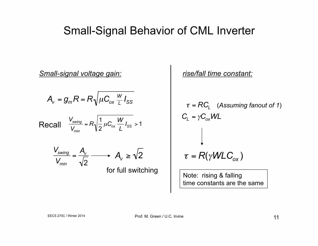
€
Av = gmR = R µCoxWL
ISS
Small-signal voltage gain:
Note: rising & falling time constants are the same
Recall
€
Vswing
Vmin
= R 12
µCoxWL
ISS > 1
for full switching
€
Vswing
Vmin
=Av
2
€
Av ≥ 2
(Assuming fanout of 1)
rise/fall time constant:
€
τ = RCL
€
CL = γCoxWL
€
τ = R(γWLCox )
Small-Signal Behavior of CML Inverter
EECS 270C / Winter 2014 Prof. M. Green / U.C. Irvine 12
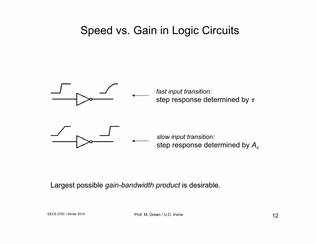
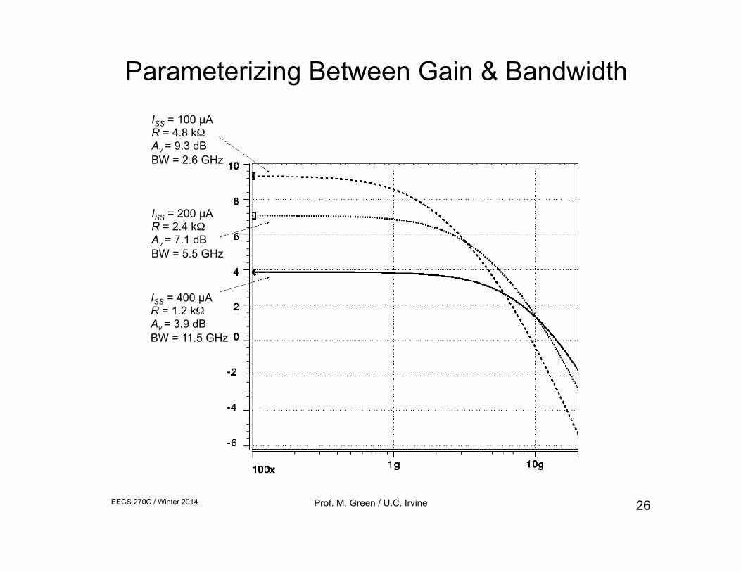
Speed vs. Gain in Logic Circuits
Largest possible gain-bandwidth product is desirable.
fast input transition: step response determined by τ
slow input transition: step response determined by Av
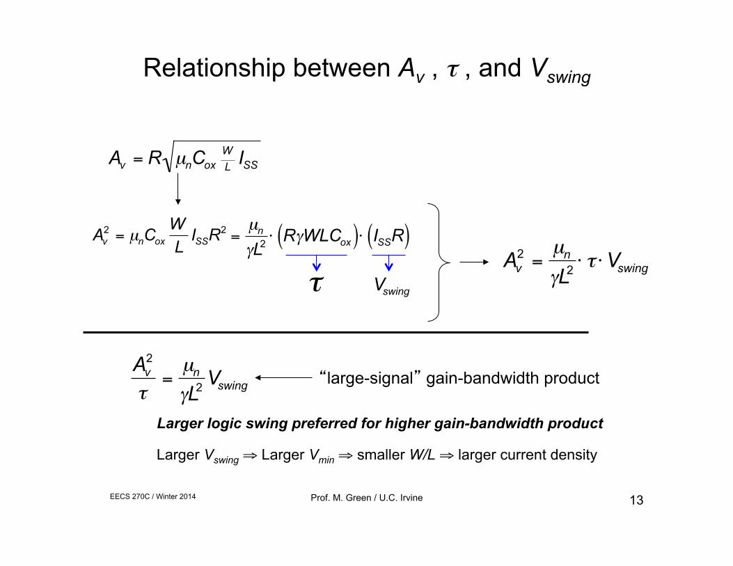
EECS 270C / Winter 2014 Prof. M. Green / U.C. Irvine 13
€
Av = R µnCoxWL ISS
€
Av2 = µnCox
WL
ISSR2
€
=µn
γL2 ⋅ RγWLCox( )⋅ ISSR( )
€
Av2 =
µn
γL2 ⋅ τ ⋅Vswing
“large-signal” gain-bandwidth product
€
Av2
τ=
µn
γL2 Vswing
Relationship between Av , τ , and Vswing
Larger logic swing preferred for higher gain-bandwidth product
Larger Vswing ⇒ Larger Vmin ⇒ smaller W/L ⇒ larger current density
€
τ
€
Vswing
EECS 270C / Winter 2014 Prof. M. Green / U.C. Irvine 14
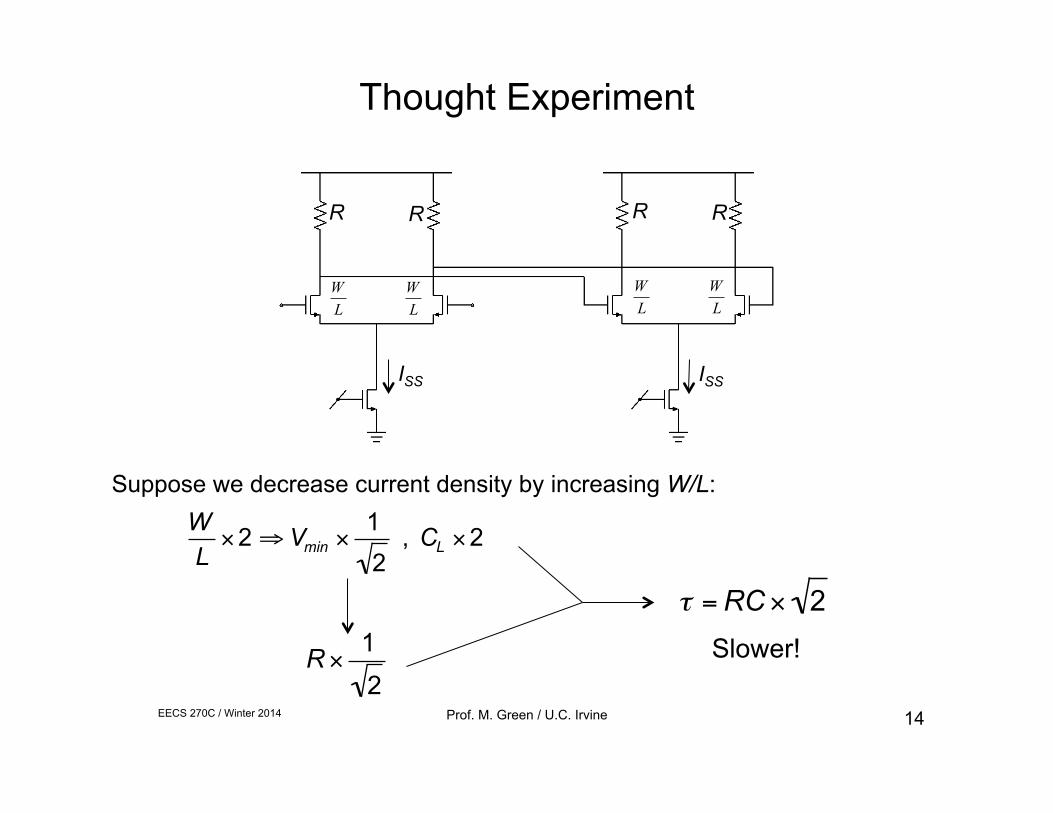
Suppose we decrease current density by increasing W/L:
€
WL×2 ⇒ Vmin ×
12
, CL ×2
€
R ×12
€
τ = RC × 2Slower!
Thought Experiment
R R
€
WL
€
WL
R R
€
WL
€
WL
ISS ISS
EECS 270C / Winter 2014 Prof. M. Green / U.C. Irvine 15
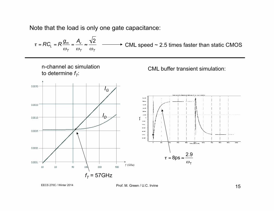
Note that the load is only one gate capacitance:
CML speed ~ 2.5 times faster than static CMOS
IG
ID
fT = 57GHz
n-channel ac simulation to determine fT:
CML buffer transient simulation:
€
τ = RCL = R gm
ωT
=Av
ωT
≈2
ωT
€
τ = 8ps ≈ 2.9ωT
EECS 270C / Winter 2014 Prof. M. Green / U.C. Irvine 16
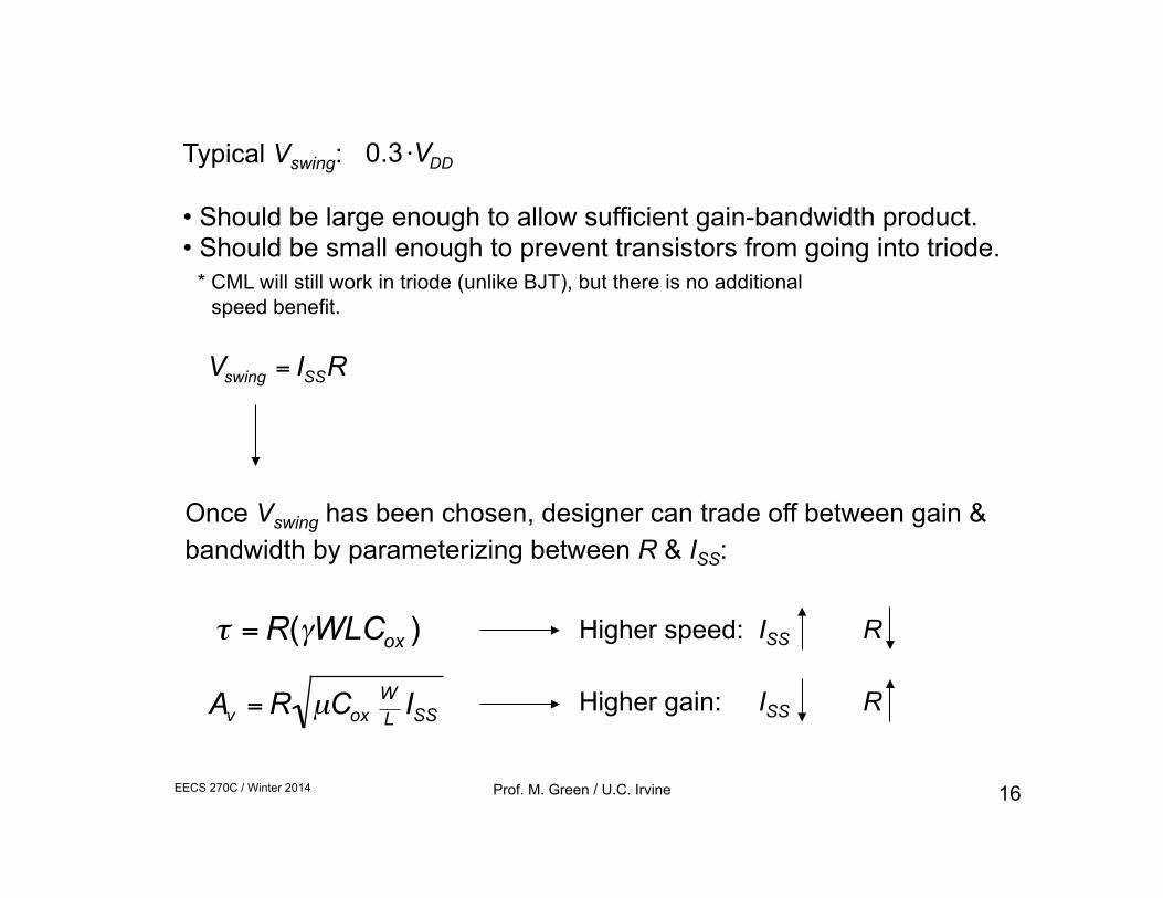
Typical Vswing: • Should be large enough to allow sufficient gain-bandwidth product. • Should be small enough to prevent transistors from going into triode. * CML will still work in triode (unlike BJT), but there is no additional speed benefit.
€
Vswing = ISSR
Once Vswing has been chosen, designer can trade off between gain & bandwidth by parameterizing between R & ISS:
Higher speed: ISS R
Higher gain: ISS R
€
Av = R µCoxWL
ISS
€
τ = R(γWLCox )
€
0.3 ⋅VDD
EECS 270C / Winter 2014 Prof. M. Green / U.C. Irvine 17
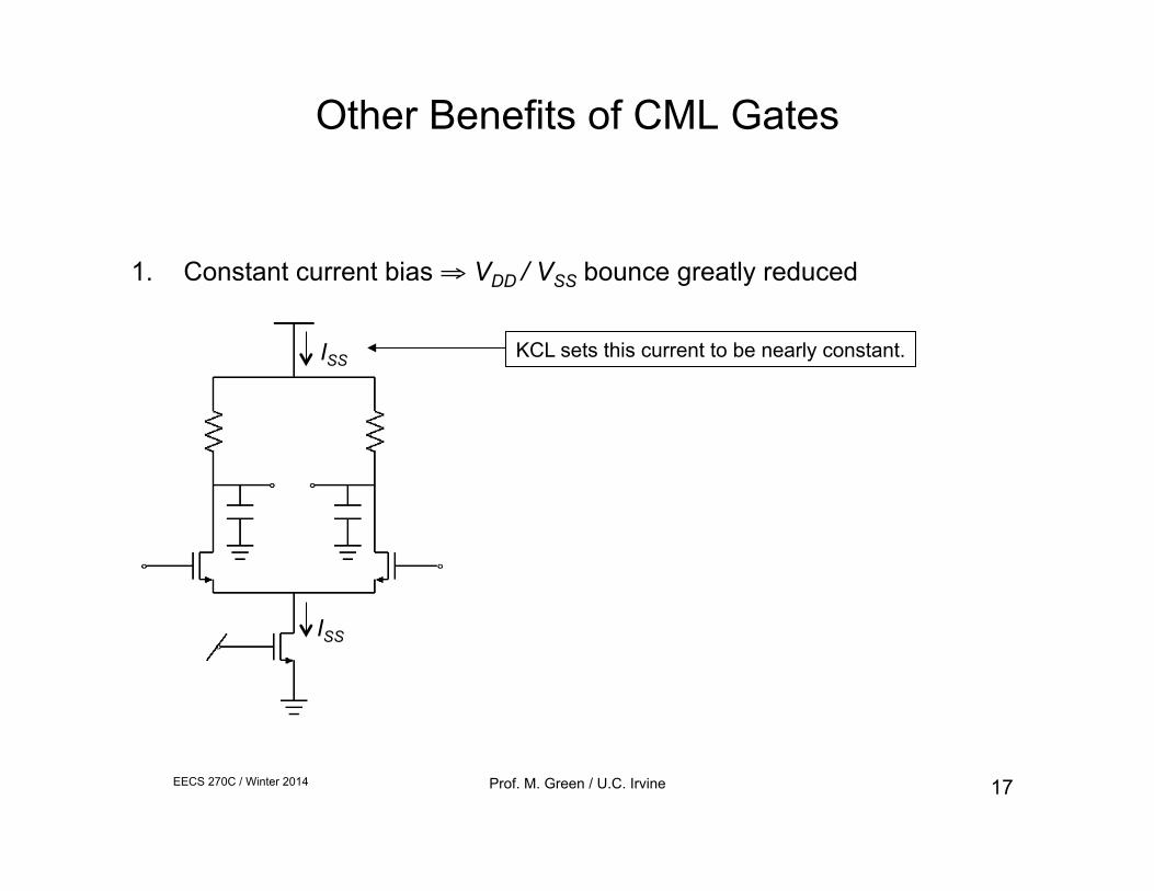
Other Benefits of CML Gates
1. Constant current bias ⇒ VDD / VSS bounce greatly reduced
KCL sets this current to be nearly constant.
ISS
ISS
EECS 270C / Winter 2014 Prof. M. Green / U.C. Irvine 18
data in clock in
Rs = 0 Ls = 0
clock out
clock out
Rs = 5Ω Ls = 5nH
clock out
data out
€
" V DD
€
" V SS
€
" V DD
€
" V SS
data out
Rs = 5Ω Ls = 5nH
EECS 270C / Winter 2014 Prof. M. Green / U.C. Irvine 19
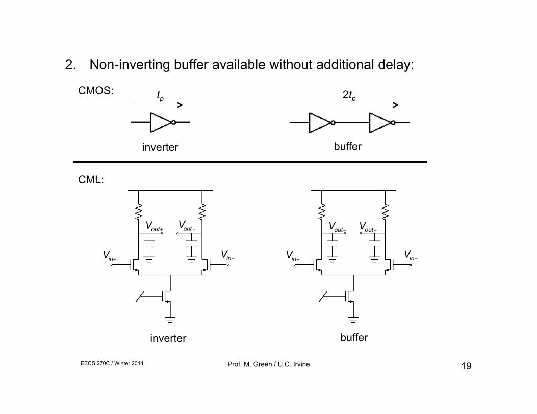
2. Non-inverting buffer available without additional delay:
CMOS:
inverter buffer
CML:
inverter buffer
€
Vin+
€
Vin−
€
Vout+
€
Vout−
€
Vin+
€
Vin−
€
Vout−
€
Vout+
tp 2tp
EECS 270C / Winter 2014 Prof. M. Green / U.C. Irvine 20
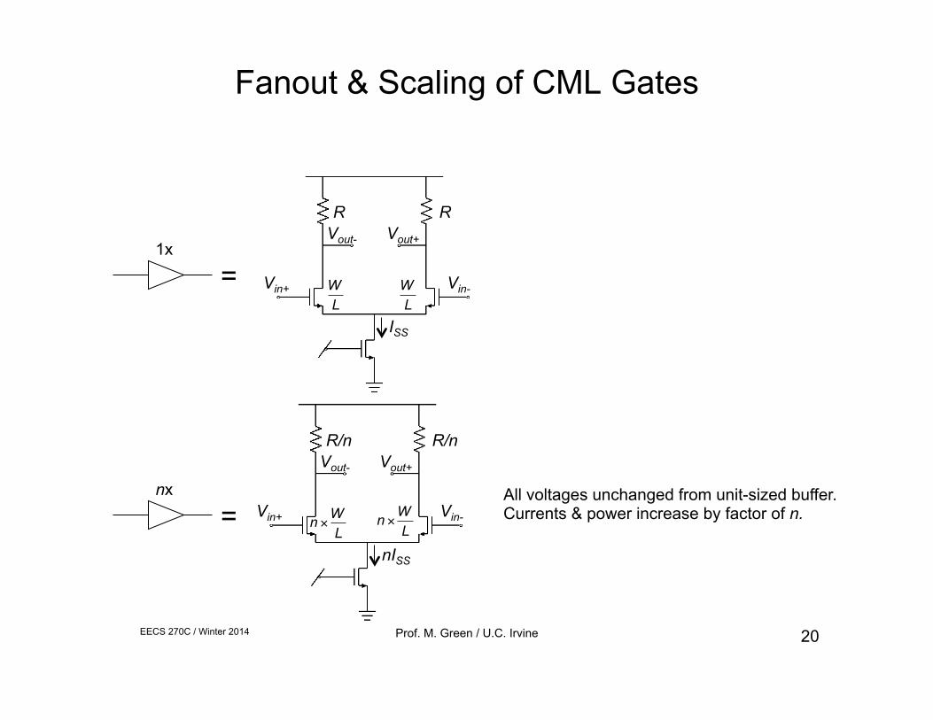
Fanout & Scaling of CML Gates
1x
=
nx
= All voltages unchanged from unit-sized buffer. Currents & power increase by factor of n.
ISS
Vin+ Vin-
Vout- Vout+ R R
€
WL
€
WL
nISS
Vin+ Vin-
Vout- Vout+ R/n R/n
€
n ×WL
€
n ×WL
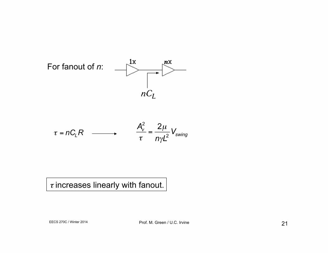
EECS 270C / Winter 2014 Prof. M. Green / U.C. Irvine 21
For fanout of n:
€
τ = nCLR
€
Av2
τ=
2µ
nγL2Vswing
τ increases linearly with fanout.
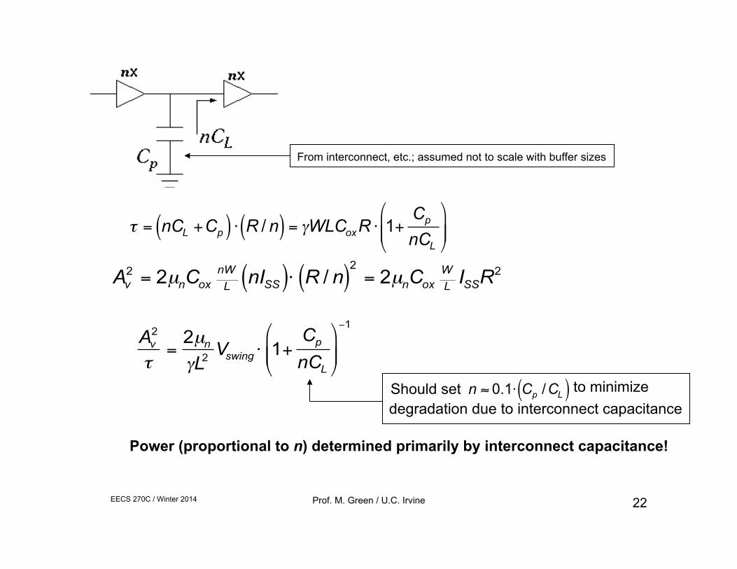
EECS 270C / Winter 2014 Prof. M. Green / U.C. Irvine 22
From interconnect, etc.; assumed not to scale with buffer sizes
€
τ = nCL +Cp( ) ⋅ R / n( ) = γWLCoxR ⋅ 1+Cp
nCL
%
& ' '
(
) * *
€
Av2 = 2µnCox
nWL nISS( )⋅ R / n( )2
= 2µnCoxWL ISSR2
€
Av2
τ=
2µn
γL2 Vswing ⋅ 1+Cp
nCL
%
& ' '
(
) * *
−1
Should set
€
n ≈ 0.1⋅ Cp /CL( )degradation due to interconnect capacitance
to minimize
Power (proportional to n) determined primarily by interconnect capacitance!
EECS 270C / Winter 2014 Prof. M. Green / U.C. Irvine 23
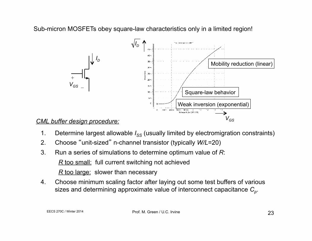
Sub-micron MOSFETs obey square-law characteristics only in a limited region!
CML buffer design procedure:
1. Determine largest allowable ISS (usually limited by electromigration constraints) 2. Choose “unit-sized” n-channel transistor (typically W/L=20) 3. Run a series of simulations to determine optimum value of R:
R too small: full current switching not achieved R too large: slower than necessary
4. Choose minimum scaling factor after laying out some test buffers of various sizes and determining approximate value of interconnect capacitance Cp.
VGS
€
ID
Mobility reduction (linear)
Square-law behavior
Weak inversion (exponential)
+ _ VGS
€
ID
EECS 270C / Winter 2014 Prof. M. Green / U.C. Irvine 24
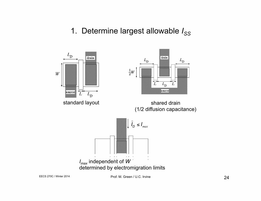
1. Determine largest allowable ISS
€
I D ≤ Imax
standard layout shared drain (1/2 diffusion capacitance)
Imax independent of W determined by electromigration limits
EECS 270C / Winter 2014 Prof. M. Green / U.C. Irvine 25
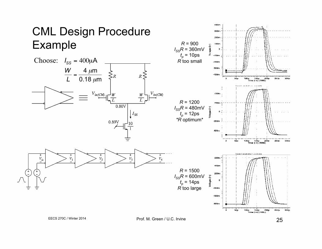
R = 1200 ISSR = 480mV
tp = 12ps *R optimum*
R = 900 ISSR = 360mV
tp = 10ps R too small
R = 1500 ISSR = 600mV
tp = 14ps R too large
CML Design Procedure Example
€
ISS = 400µA
€
WL
=4 µm
0.18 µm
Choose:
EECS 270C / Winter 2014 Prof. M. Green / U.C. Irvine 26
Parameterizing Between Gain & Bandwidth ISS = 100 µA R = 4.8 kΩ Av = 9.3 dB BW = 2.6 GHz
ISS = 200 µA R = 2.4 kΩ Av = 7.1 dB BW = 5.5 GHz
ISS = 400 µA R = 1.2 kΩ Av = 3.9 dB BW = 11.5 GHz
EECS 270C / Winter 2014 Prof. M. Green / U.C. Irvine 27
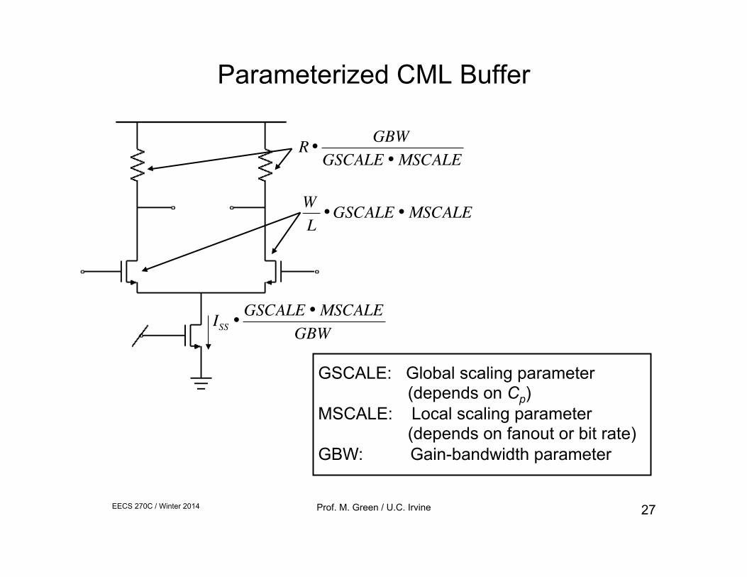
€
R •GBW
GSCALE •MSCALE
€
ISS •GSCALE •MSCALE
GBW
€
WL
•GSCALE •MSCALE
GSCALE: Global scaling parameter (depends on Cp) MSCALE: Local scaling parameter (depends on fanout or bit rate) GBW: Gain-bandwidth parameter
Parameterized CML Buffer
EECS 270C / Winter 2014 Prof. M. Green / U.C. Irvine 28
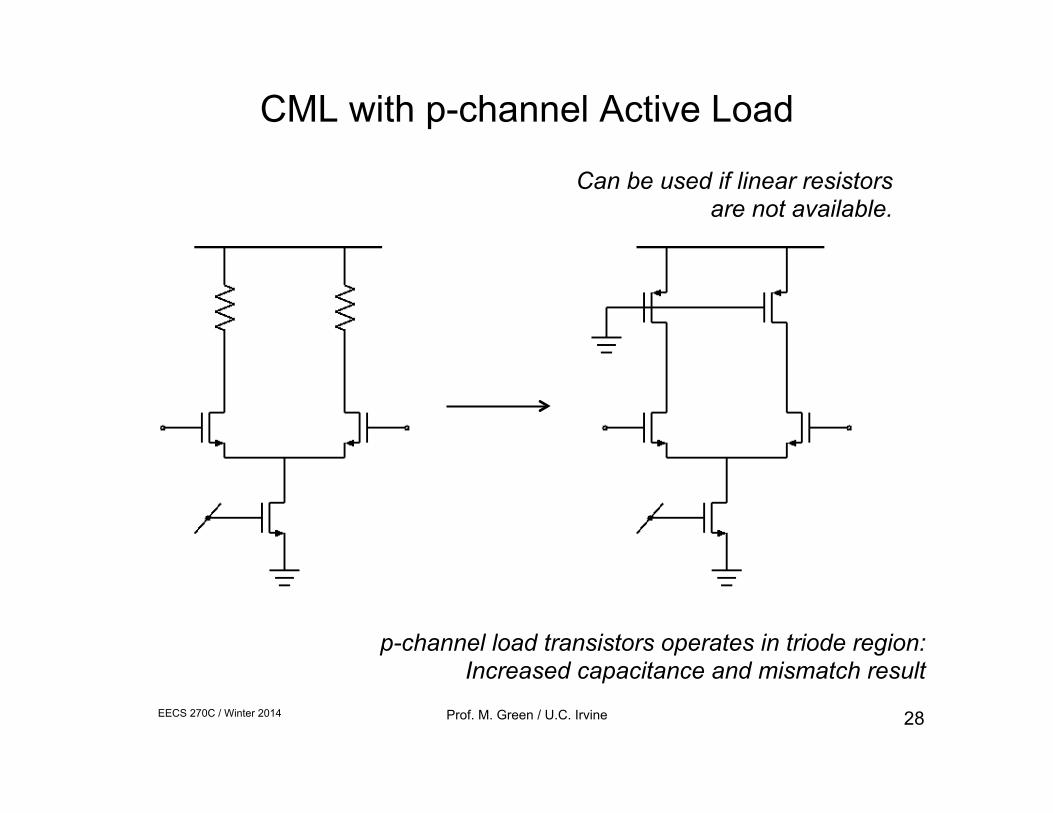
CML with p-channel Active Load
p-channel load transistors operates in triode region: Increased capacitance and mismatch result
Can be used if linear resistors are not available.
EECS 270C / Winter 2014 Prof. M. Green / U.C. Irvine 29
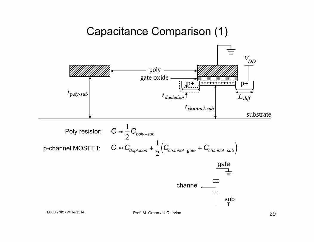
Capacitance Comparison (1)
Poly resistor:
p-channel MOSFET:
€
C ≈12
Cpoly−sub
€
C ≈Cdepletion +12
Cchannel−gate + Cchannel−sub( )gate
sub
channel
EECS 270C / Winter 2014 Prof. M. Green / U.C. Irvine 30
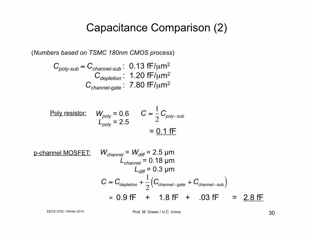
Cpoly-sub ≈ Cchannel-sub : 0.13 fF/µm2
Cdepletion : 1.20 fF/µm2
Cchannel-gate : 7.80 fF/µm2
Poly resistor:
p-channel MOSFET:
€
C ≈12
Cpoly−sub
€
C ≈Cdepletion +12
Cchannel−gate + Cchannel−sub( )
Wchannel = Wdiff = 2.5 µm Lchannel = 0.18 µm
Ldiff = 0.3 µm
Wpoly = 0.6 Lpoly = 2.5
= 0.1 fF
= 0.9 fF + 1.8 fF + .03 fF = 2.8 fF
Capacitance Comparison (2)
(Numbers based on TSMC 180nm CMOS process)
EECS 270C / Winter 2014 Prof. M. Green / U.C. Irvine 31
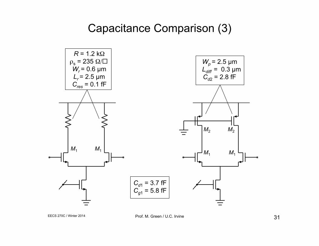
R = 1.2 kΩ ρs = 235 Ω/! Wr = 0.6 µm Lr = 2.5 µm Cres = 0.1 fF
Wp = 2.5 µm Ldiff = 0.3 µm
Cd2 = 2.8 fF
M2 M2
M1 M1 M1 M1
Cd1 = 3.7 fF Cg1 = 5.8 fF
Capacitance Comparison (3)
EECS 270C / Winter 2014 Prof. M. Green / U.C. Irvine 32
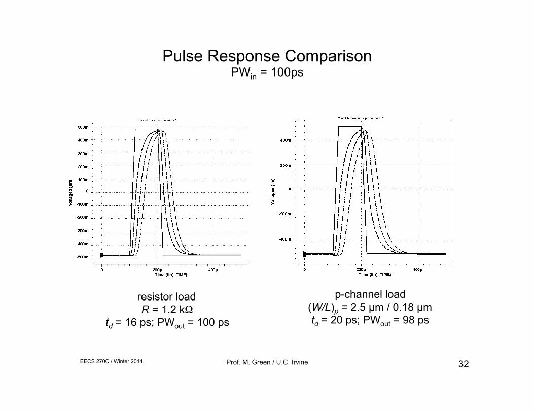
Pulse Response Comparison PWin = 100ps
resistor load R = 1.2 kΩ
td = 16 ps; PWout = 100 ps
p-channel load (W/L)p = 2.5 µm / 0.18 µm td = 20 ps; PWout = 98 ps
EECS 270C / Winter 2014 Prof. M. Green / U.C. Irvine 33
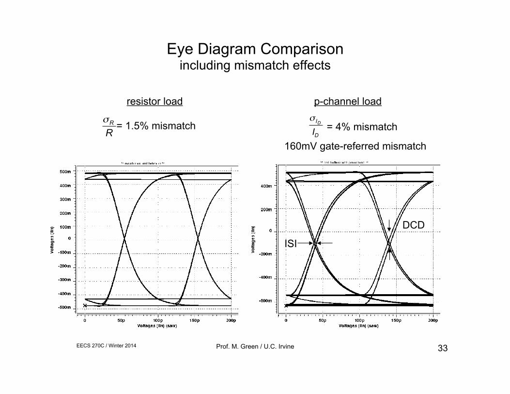
Eye Diagram Comparison including mismatch effects
resistor load
= 1.5% mismatch
€
σR
R160mV gate-referred mismatch
€
σ ID
ID= 4% mismatch
p-channel load
ISI
DCD
EECS 270C / Winter 2014 Prof. M. Green / U.C. Irvine 34
MA MA
MB MB
MA MA
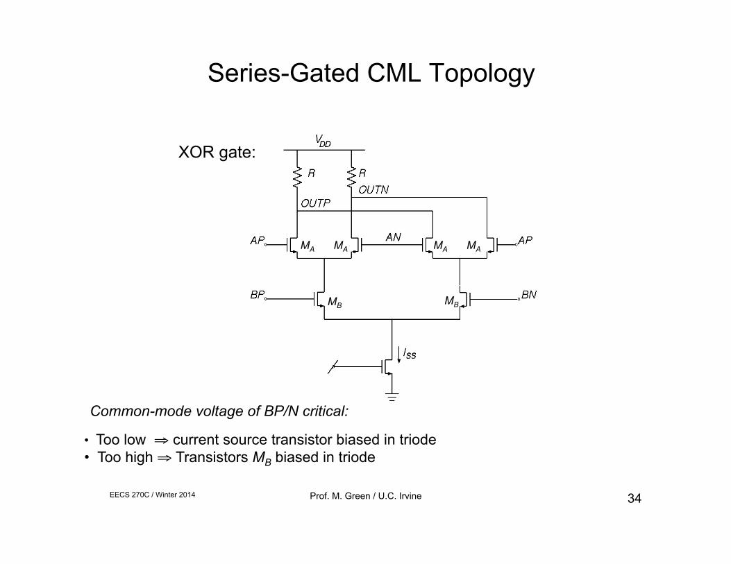
Series-Gated CML Topology
XOR gate:
Common-mode voltage of BP/N critical:
• Too low ⇒ current source transistor biased in triode • Too high ⇒ Transistors MB biased in triode
EECS 270C / Winter 2014 Prof. M. Green / U.C. Irvine 35
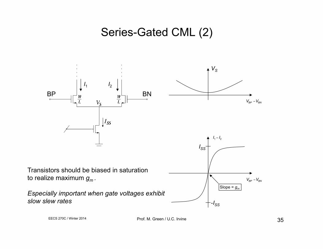
€
VBP −VBN
VS
I1 I2
€
I1 − I2
-ISS
ISS
Slope = gm
Transistors should be biased in saturation to realize maximum gm . Especially important when gate voltages exhibit slow slew rates
BP BN
€
VBP −VBN
Series-Gated CML (2)
EECS 270C / Winter 2014 Prof. M. Green / U.C. Irvine 36
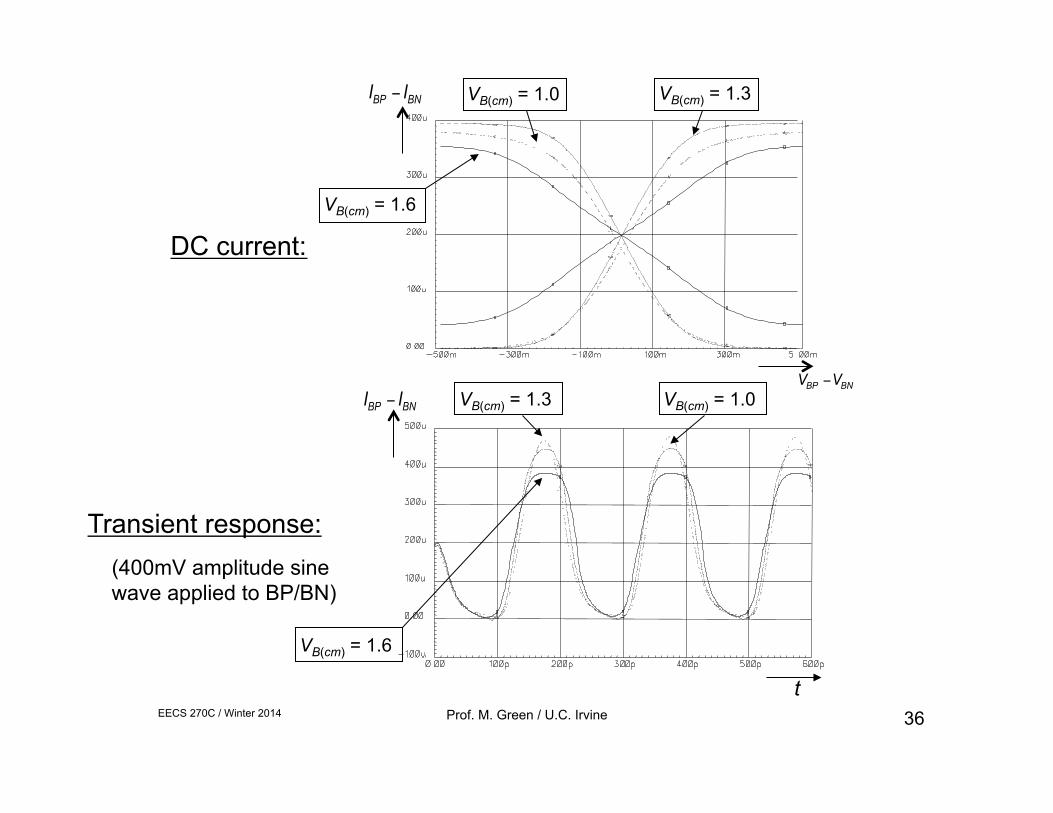
VB(cm) = 1.6
VB(cm) = 1.3 VB(cm) = 1.0
€
VBP −VBN
t
VB(cm) = 1.6
VB(cm) = 1.3 VB(cm) = 1.0
DC current:
Transient response: (400mV amplitude sine wave applied to BP/BN)
€
IBP − IBN
€
IBP − IBN
EECS 270C / Winter 2014 Prof. M. Green / U.C. Irvine 37
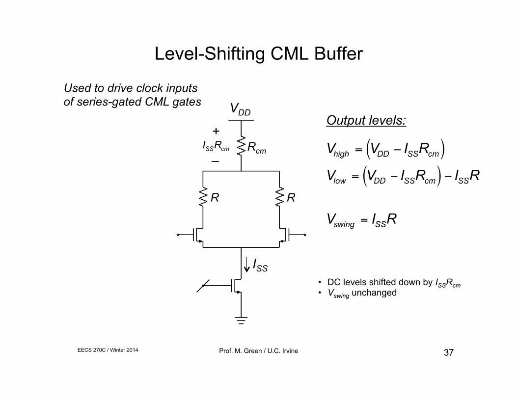
Level-Shifting CML Buffer
VDD
Rcm
ISS
R R
+
_
€
ISSRcm
Output levels:
€
Vhigh = VDD − ISSRcm( )
€
Vlow = VDD − ISSRcm( ) − ISSR
Used to drive clock inputs of series-gated CML gates
€
Vswing = ISSR
• DC levels shifted down by ISSRcm • Vswing unchanged
EECS 270C / Winter 2014 Prof. M. Green / U.C. Irvine 38
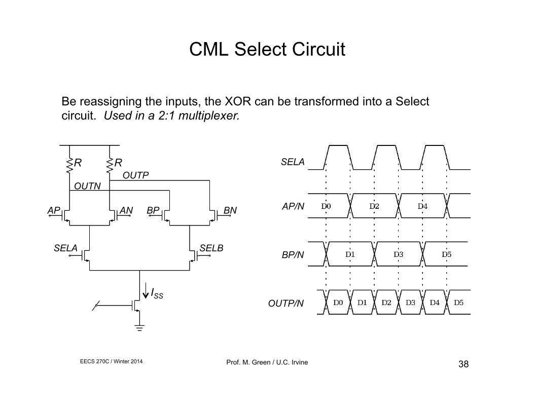
Be reassigning the inputs, the XOR can be transformed into a Select circuit. Used in a 2:1 multiplexer.
CML Select Circuit
ISS
R R
AP AN BP BN
SELA SELB
OUTP OUTN
SELA
AP/N
BP/N
OUTP/N
EECS 270C / Winter 2014 Prof. M. Green / U.C. Irvine 39
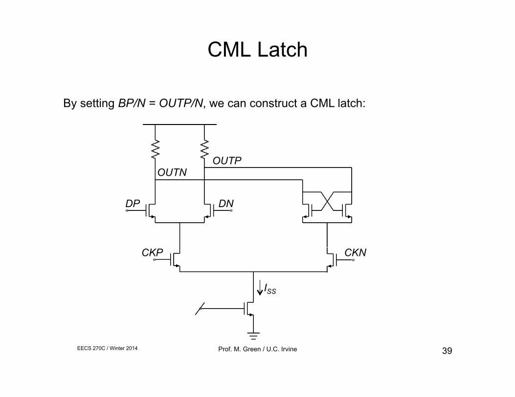
CML Latch
By setting BP/N = OUTP/N, we can construct a CML latch:
ISS
DP DN
OUTP OUTN
CKP CKN
EECS 270C / Winter 2014 Prof. M. Green / U.C. Irvine 40
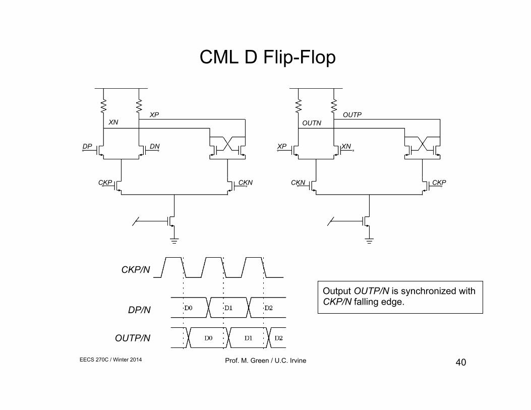
CML D Flip-Flop
Output OUTP/N is synchronized with CKP/N falling edge.
DP DN
CKP CKN
XN XP
XP XN
OUTN OUTP
CKP CKN
CKP/N
DP/N
OUTP/N
EECS 270C / Winter 2014 Prof. M. Green / U.C. Irvine 41
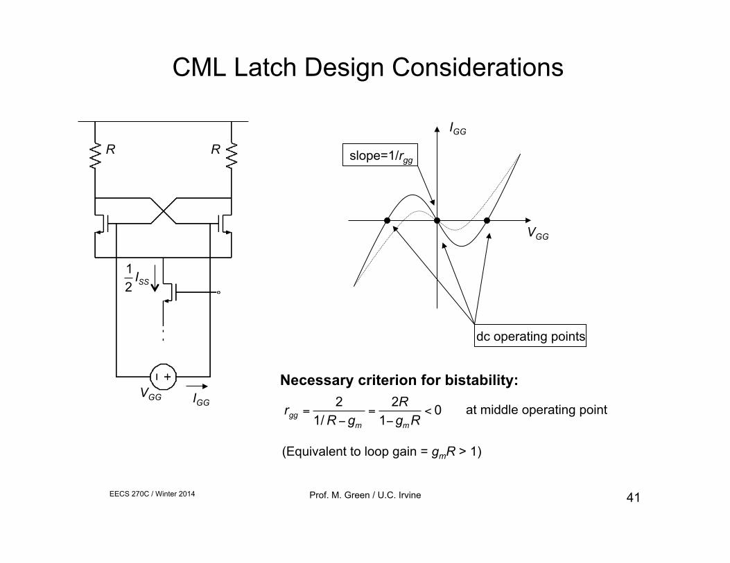
CML Latch Design Considerations
IGG
VGG
dc operating points
Necessary criterion for bistability:
€
rgg =2
1/ R −gm
=2R
1−gmR< 0 at middle operating point
(Equivalent to loop gain = gmR > 1)
slope=1/rgg
IGG VGG
€
12
ISS
R R
EECS 270C / Winter 2014 Prof. M. Green / U.C. Irvine 42
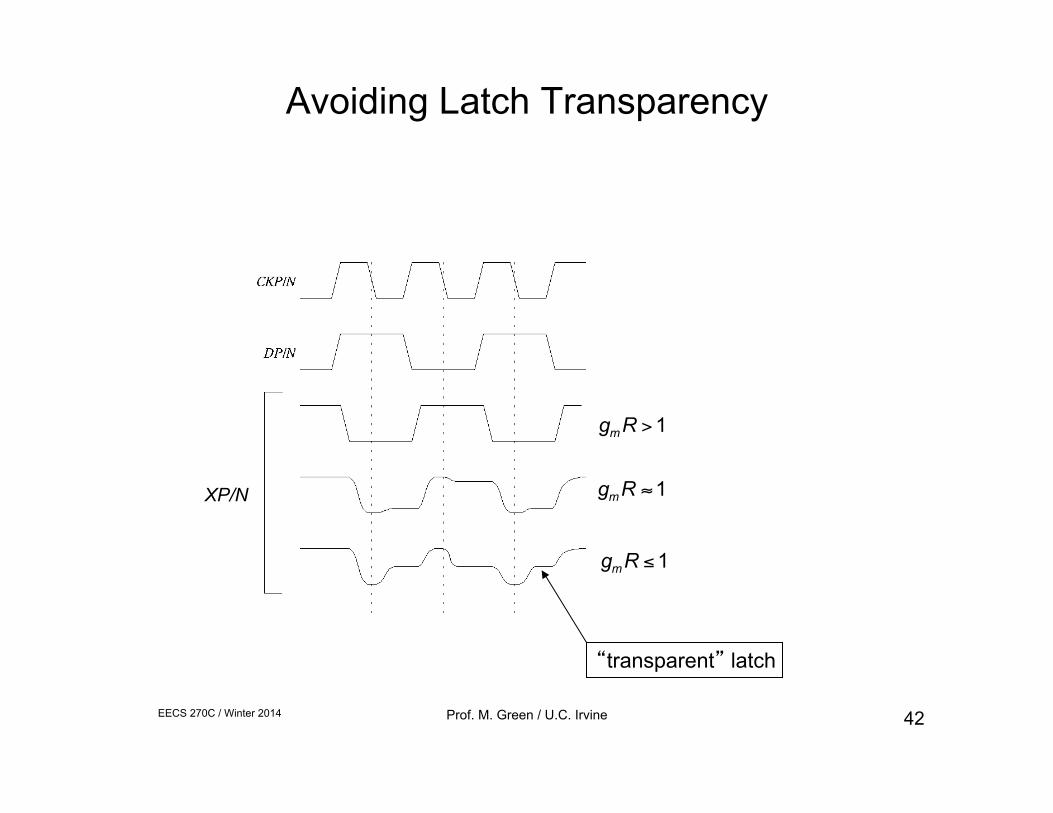
€
gmR > 1
€
gmR ≈1
€
gmR ≤1
“transparent” latch
Avoiding Latch Transparency
XP/N
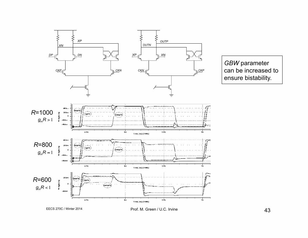
EECS 270C / Winter 2014 Prof. M. Green / U.C. Irvine 43
R=1000
R=800
R=600
GBW parameter can be increased to ensure bistability.
€
gmR > 1
€
gmR ≈ 1
€
gmR < 1
DP DN
CKP CKN
QINQIP
QIP QIN
OUTNOUTP
CKPCKN
XP XN
XP XN
EECS 270C / Winter 2014 Prof. M. Green / U.C. Irvine 44
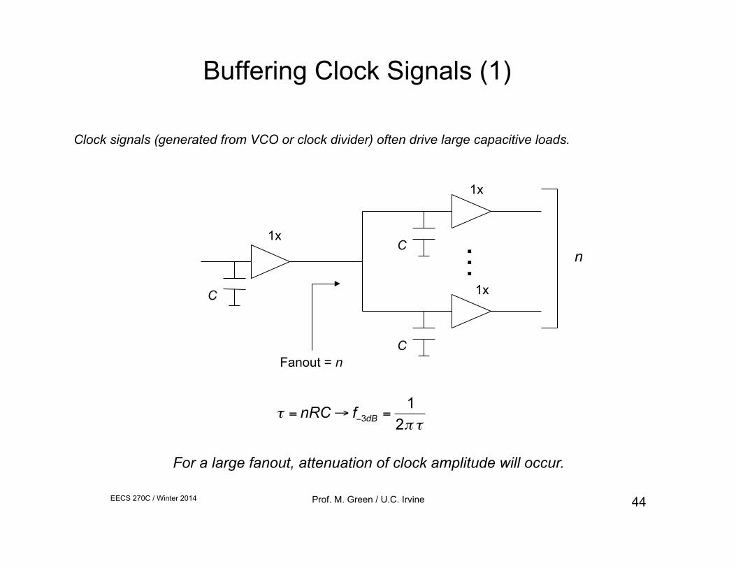
Buffering Clock Signals (1)
Clock signals (generated from VCO or clock divider) often drive large capacitive loads.
1x
…
Fanout = n
€
τ = nRC → f−3dB =1
2π τ
C
C
C
For a large fanout, attenuation of clock amplitude will occur.
1x
1x
n
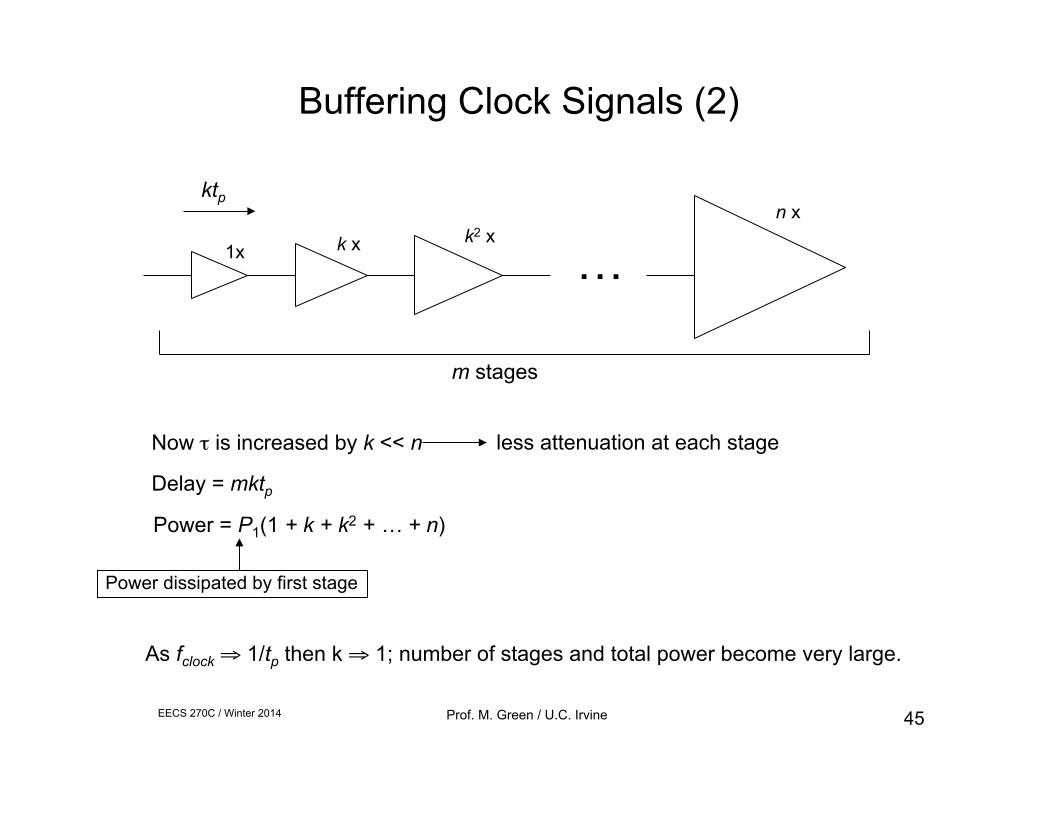
EECS 270C / Winter 2014 Prof. M. Green / U.C. Irvine 45
… 1x k x k2 x n x
m stages
Now τ is increased by k << n less attenuation at each stage
Delay = mktp
ktp
Power = P1(1 + k + k2 + … + n)
As fclock ⇒ 1/tp then k ⇒ 1; number of stages and total power become very large.
Power dissipated by first stage
Buffering Clock Signals (2)
EECS 270C / Winter 2014 Prof. M. Green / U.C. Irvine 46
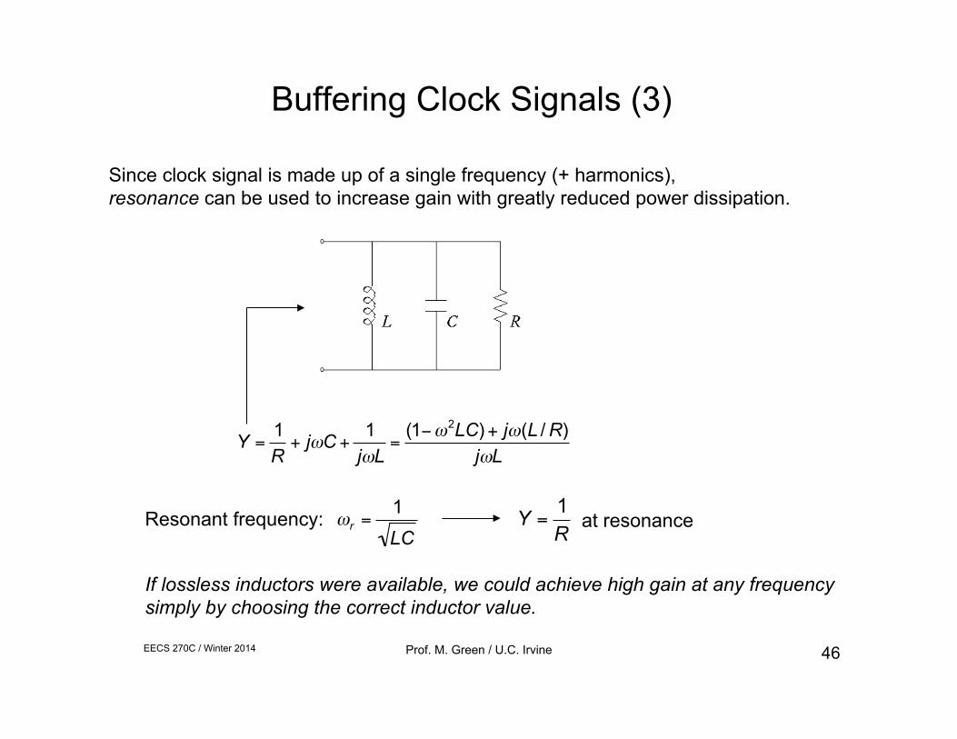
Since clock signal is made up of a single frequency (+ harmonics), resonance can be used to increase gain with greatly reduced power dissipation.
€
Y =1R
+ jωC +1
jωL=
(1−ω2LC) + jω(L / R)jωL
Resonant frequency:
€
ωr =1LC
€
Y =1R
at resonance
If lossless inductors were available, we could achieve high gain at any frequency simply by choosing the correct inductor value.
Buffering Clock Signals (3)
EECS 270C / Winter 2014 Prof. M. Green / U.C. Irvine 47
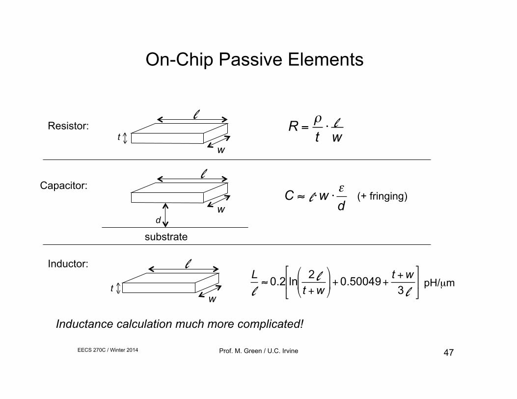
On-Chip Passive Elements
€
R =ρt⋅w
Resistor:
€
C ≈ ⋅w ⋅εd
Capacitor:
d w
substrate
(+ fringing)
Inductor:
t
t w
l
w
Inductance calculation much more complicated!
l
l
l
l
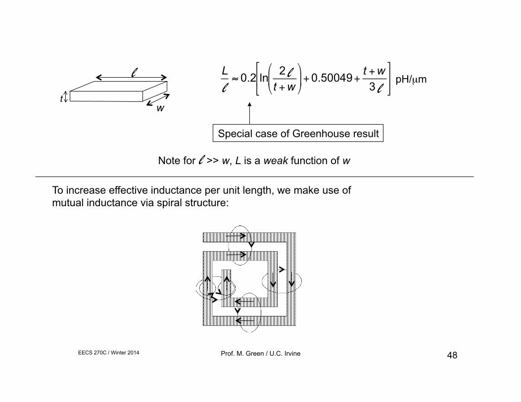
€
L≈ 0.2 ln 2
t + w
#
$ %
&
' ( + 0.50049+
t + w3
)
* +
,
- . pH/µm l
l l
EECS 270C / Winter 2014 Prof. M. Green / U.C. Irvine 48
t w
Special case of Greenhouse result
Note for l >> w, L is a weak function of w
To increase effective inductance per unit length, we make use of mutual inductance via spiral structure:
€
L≈ 0.2 ln 2
t + w
#
$ %
&
' ( + 0.50049+
t + w3
)
* +
,
- . pH/µm l
l l
l
EECS 270C / Winter 2014 Prof. M. Green / U.C. Irvine 49
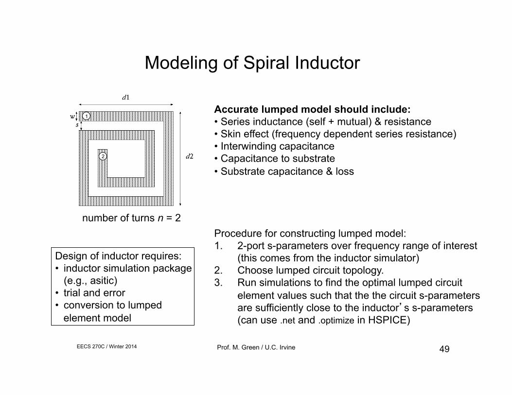
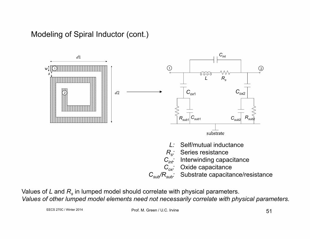
Modeling of Spiral Inductor
Design of inductor requires: • inductor simulation package (e.g., asitic) • trial and error • conversion to lumped
element model
number of turns n = 2
1
2
Accurate lumped model should include: • Series inductance (self + mutual) & resistance • Skin effect (frequency dependent series resistance) • Interwinding capacitance • Capacitance to substrate • Substrate capacitance & loss
Procedure for constructing lumped model: 1. 2-port s-parameters over frequency range of interest
(this comes from the inductor simulator) 2. Choose lumped circuit topology. 3. Run simulations to find the optimal lumped circuit
element values such that the the circuit s-parameters are sufficiently close to the inductor’s s-parameters (can use .net and .optimize in HSPICE)
EECS 270C / Winter 2014 Prof. M. Green / U.C. Irvine 50
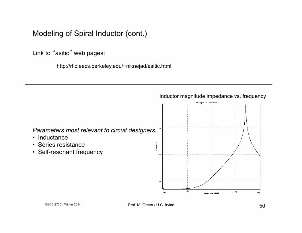
Parameters most relevant to circuit designers: • Inductance • Series resistance • Self-resonant frequency
http://rfic.eecs.berkeley.edu/~niknejad/asitic.html
Link to “asitic” web pages:
Modeling of Spiral Inductor (cont.)
Inductor magnitude impedance vs. frequency
EECS 270C / Winter 2014 Prof. M. Green / U.C. Irvine 51
1
2
Cint
L Rs
Cox2 Cox1
Csub1 Csub2 Rsub1 Rsub2
1 2
L: Rs:
Cint: Cox:
Csub/Rsub:
Self/mutual inductance Series resistance Interwinding capacitance Oxide capacitance Substrate capacitance/resistance
Values of L and Rs in lumped model should correlate with physical parameters. Values of other lumped model elements need not necessarily correlate with physical parameters.
Modeling of Spiral Inductor (cont.)
EECS 270C / Winter 2014 Prof. M. Green / U.C. Irvine 52
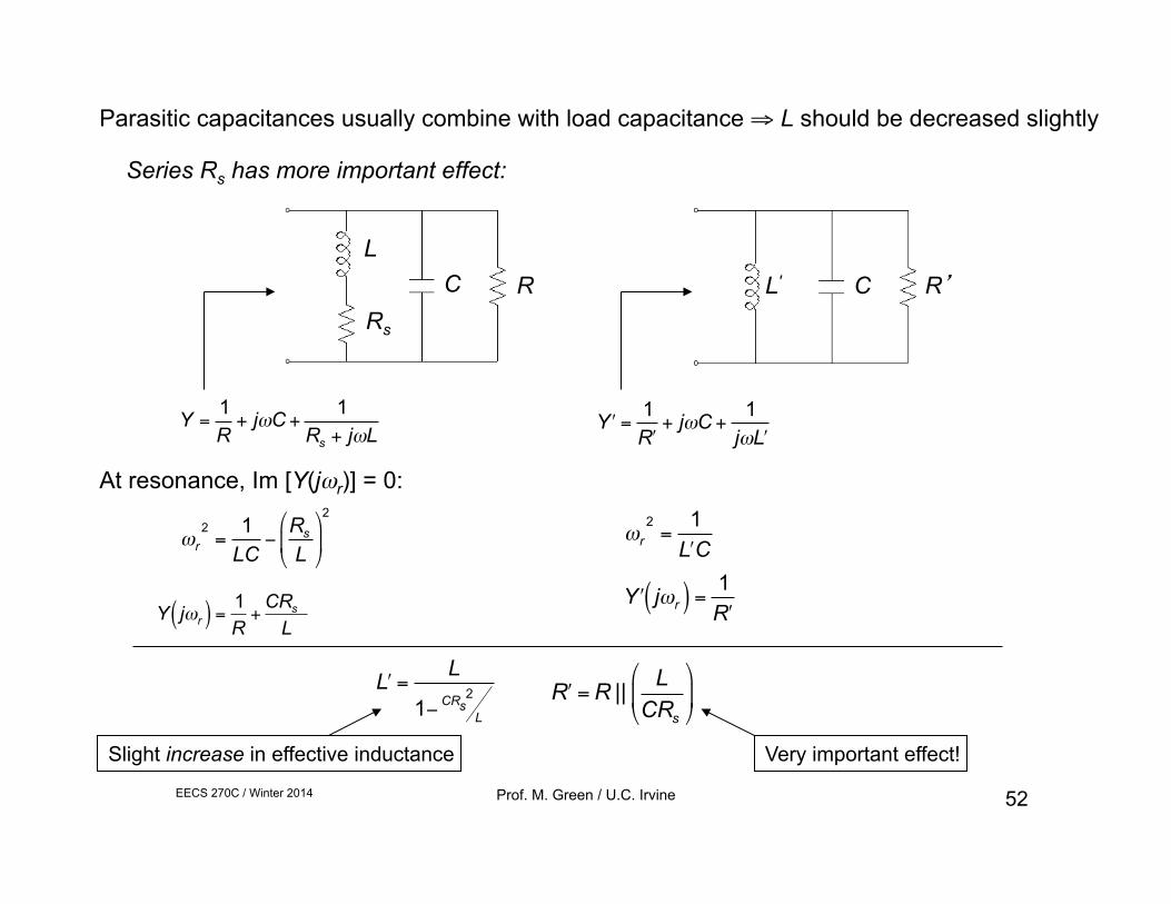
Parasitic capacitances usually combine with load capacitance ⇒ L should be decreased slightly
Series Rs has more important effect:
€
Y =1R
+ jωC +1
Rs + jωL
L
Rs
C R
€
" Y =1" R
+ jωC +1
jω " L
R’ C L'
At resonance, Im [Y(jωr)] = 0:
€
ωr2
=1
LC−
Rs
L
$
% &
'
( )
2
€
ωr2
=1# L C
€
Y jωr( ) =1R
+CRs
L
€
" Y jωr( ) =1" R
€
" L =L
1− CRs2
L
€
" R = R || LCRs
#
$ %
&
' (
Slight increase in effective inductance Very important effect!
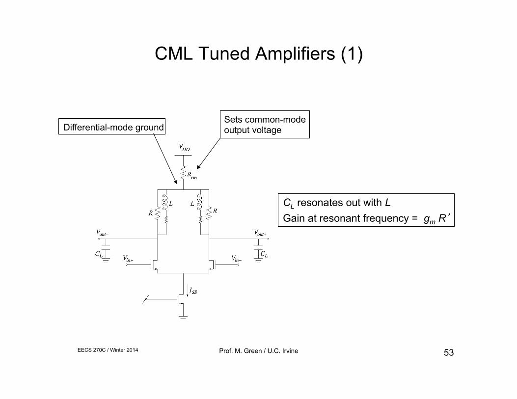
EECS 270C / Winter 2014 Prof. M. Green / U.C. Irvine 53
Differential-mode ground Sets common-mode output voltage
Gain at resonant frequency = gm R’
CL resonates out with L
CML Tuned Amplifiers (1)
EECS 270C / Winter 2014 Prof. M. Green / U.C. Irvine 54
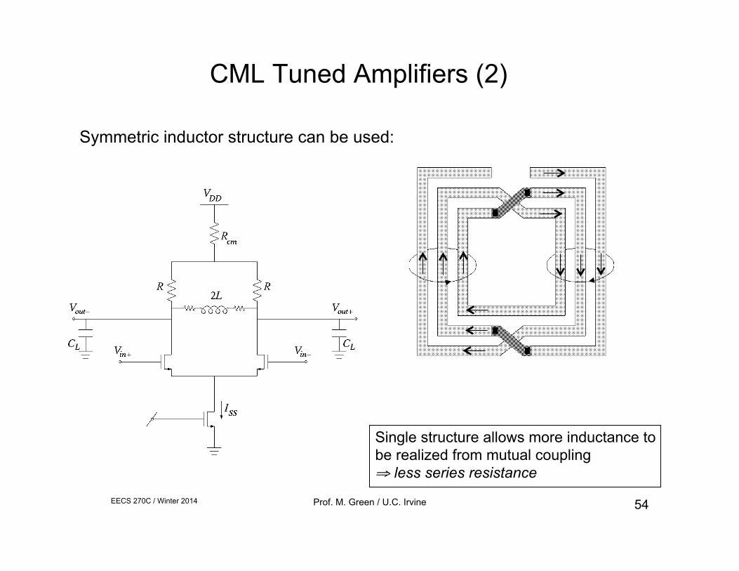
Symmetric inductor structure can be used:
Single structure allows more inductance to be realized from mutual coupling ⇒ less series resistance
CML Tuned Amplifiers (2)
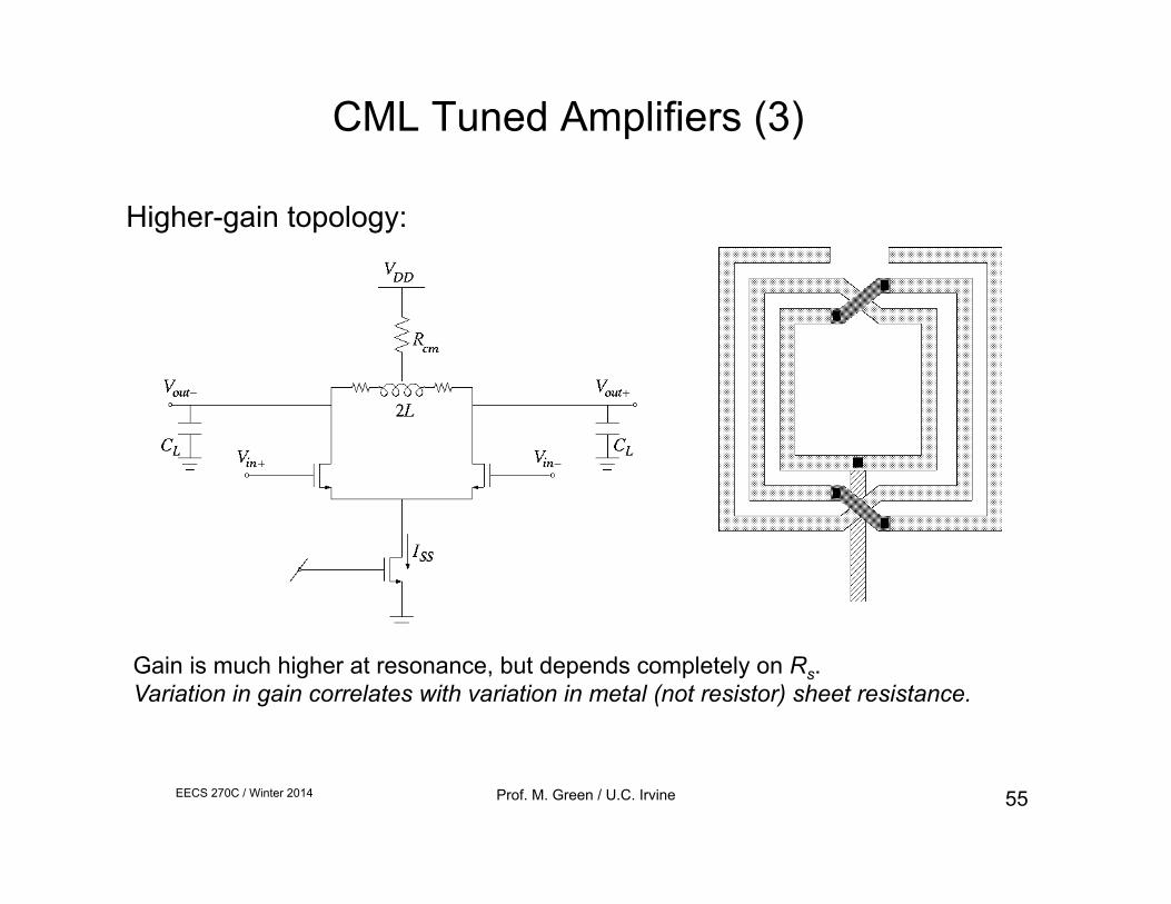
EECS 270C / Winter 2014 Prof. M. Green / U.C. Irvine 55
Gain is much higher at resonance, but depends completely on Rs. Variation in gain correlates with variation in metal (not resistor) sheet resistance.
CML Tuned Amplifiers (3)
Higher-gain topology:
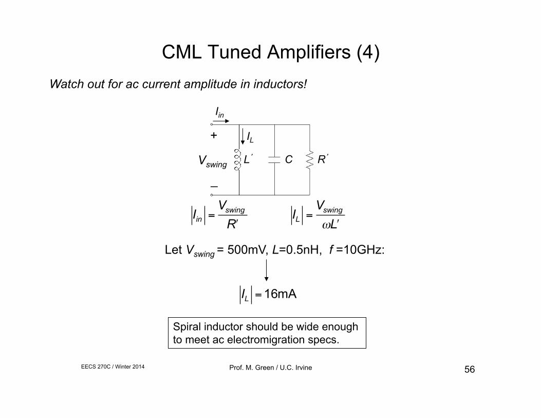
EECS 270C / Winter 2014 Prof. M. Green / U.C. Irvine 56
R’ C L’ Vswing
+
_
Iin
IL
Let Vswing = 500mV, L=0.5nH, f =10GHz:
Spiral inductor should be wide enough to meet ac electromigration specs.
€
Iin =Vswing
" R
€
IL =Vswing
ω # L
€
IL = 16mA
Watch out for ac current amplitude in inductors!
CML Tuned Amplifiers (4)
EECS 270C / Winter 2014 Prof. M. Green / U.C. Irvine 57
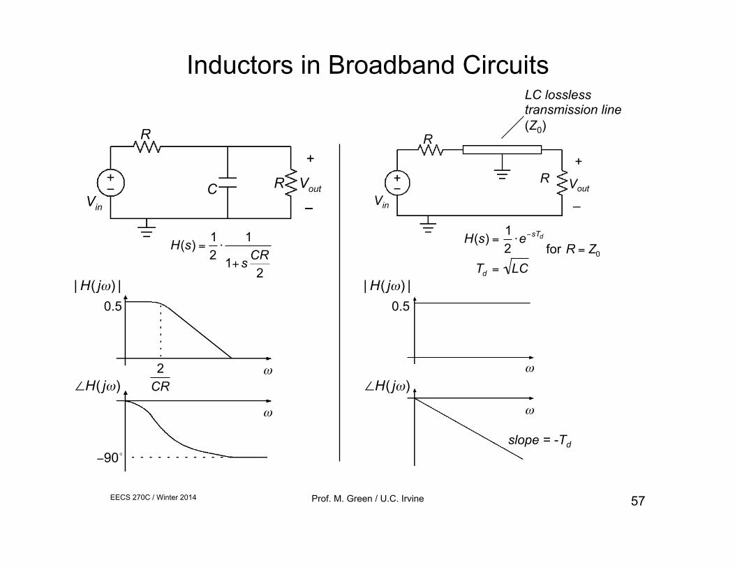
Inductors in Broadband Circuits
R
R
Vin Vout
+
_
LC lossless transmission line (Z0) R
RCVin
Vout
+
€
H(s) =12⋅
1
1+ s CR2
ω
ω
€
| H( jω) |
€
∠H( jω)
€
−90!
€
2CR
€
H(s) =12⋅e−sTd
Td = LC
€
for R = Z0
€
| H( jω) |
€
∠H( jω)
0.5 0.5
ω
ω
slope = -Td
EECS 270C / Winter 2014 Prof. M. Green / U.C. Irvine 58
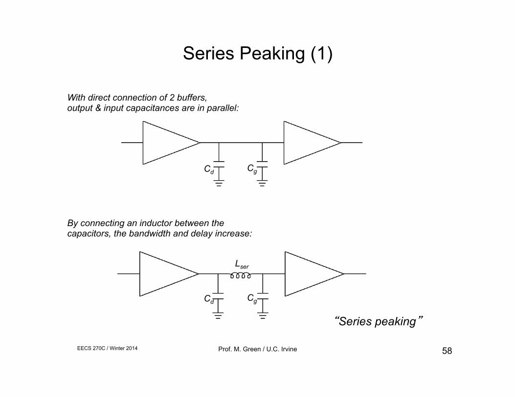
Series Peaking (1)
Cd Cg
Cd Cg
Lser
With direct connection of 2 buffers, output & input capacitances are in parallel:
By connecting an inductor between the capacitors, the bandwidth and delay increase:
“Series peaking”
EECS 270C / Winter 2014 Prof. M. Green / U.C. Irvine 59
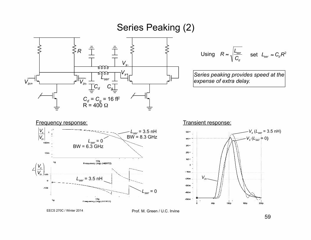
Series Peaking (2)
Cd = Cg = 16 fF R = 400 Ω
Lser
Cd Cg
R
Vin+ Vin-
Vx+
Vx-
€
R ≈Lser
Cd
Using
€
Lser ≈CdR2set
€
Vx
Vin
€
∠Vx
Vin
#
$ %
&
' (
Lser = 0 BW = 6.3 GHz
Lser = 3.5 nH BW = 8.3 GHz
Lser = 3.5 nH
Lser = 0
Frequency response:
Vin
Vx (Lser = 0)
Transient response: Vx (Lser = 3.5 nH)
Vin
Vx (Lser = 0)
Series peaking provides speed at the expense of extra delay.
EECS 270C / Winter 2014 Prof. M. Green / U.C. Irvine 60
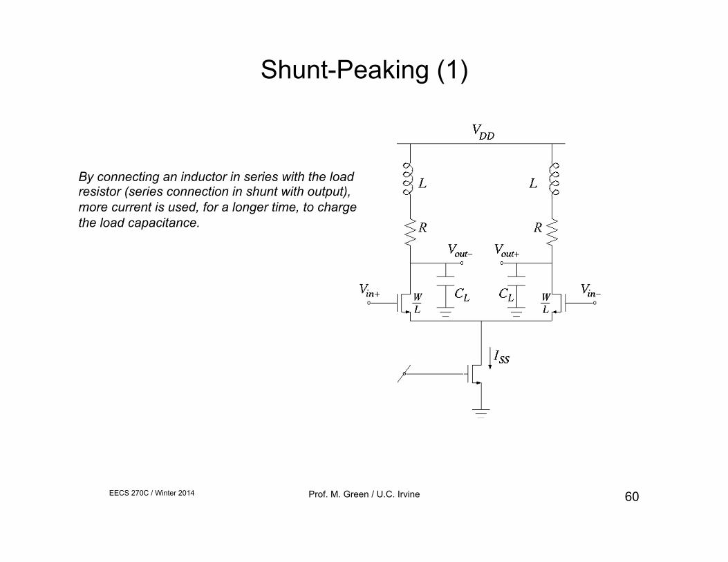
Shunt-Peaking (1)
By connecting an inductor in series with the load resistor (series connection in shunt with output), more current is used, for a longer time, to charge the load capacitance.
EECS 270C / Winter 2014 Prof. M. Green / U.C. Irvine 61
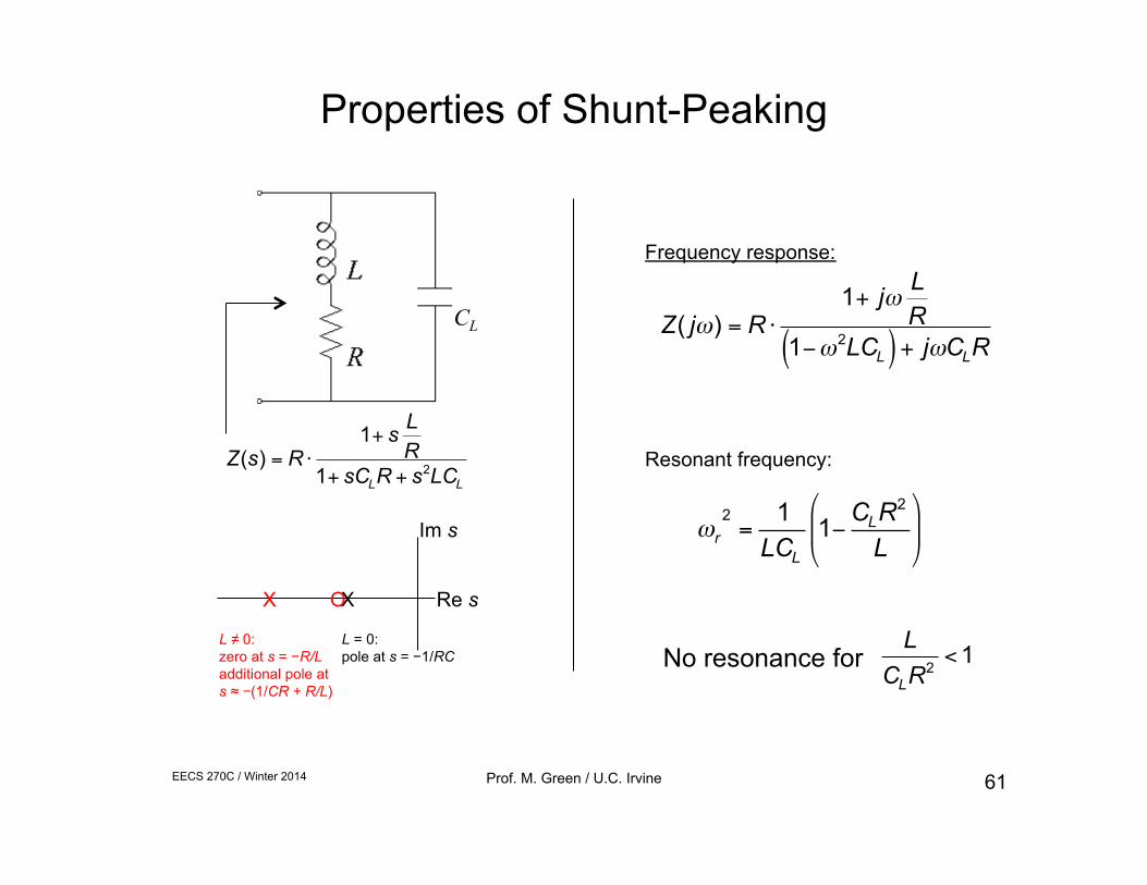
Properties of Shunt-Peaking
€
ωr2
=1
LCL
1−CLR2
L
$
% &
'
( )
Resonant frequency:
No resonance for
€
LCLR2
< 1
CL
X Re s
Im s
L = 0: pole at s = −1/RC
X O
L ≠ 0: zero at s = −R/L additional pole at s ≈ −(1/CR + R/L)
€
Z(s) = R ⋅1+ s L
R1+ sCLR + s2LCL
€
Z( jω) = R ⋅1+ jω L
R1−ω2LCL( ) + jωCLR
Frequency response:
EECS 270C / Winter 2014 Prof. M. Green / U.C. Irvine 62
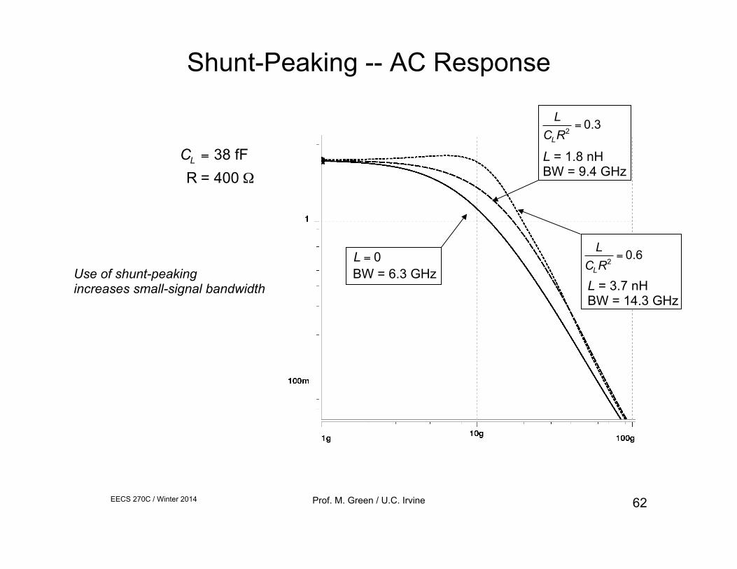
€
L = 0BW = 6.3 GHz
€
LCLR2
= 0.3
L = 1.8 nH BW = 9.4 GHz
€
LCLR2
= 0.6
L = 3.7 nH BW = 14.3 GHz
Shunt-Peaking -- AC Response
Use of shunt-peaking increases small-signal bandwidth
€
CL = 38 fFR = 400 Ω
EECS 270C / Winter 2014 Prof. M. Green / U.C. Irvine 63
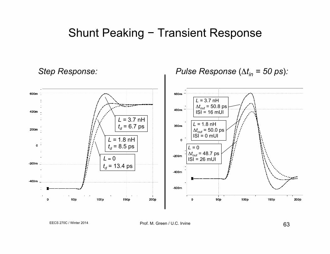
Shunt Peaking − Transient Response
Step Response:
€
L = 0td = 13.4 ps
L = 1.8 nH td = 8.5 ps
L = 3.7 nH td = 6.7 ps
Pulse Response (Δtin = 50 ps):
L = 3.7 nH Δtout = 50.8 ps ISI = 16 mUI
L = 1.8 nH Δtout = 50.0 ps ISI = 0 mUI
L = 0 Δtout = 48.7 ps ISI = 26 mUI
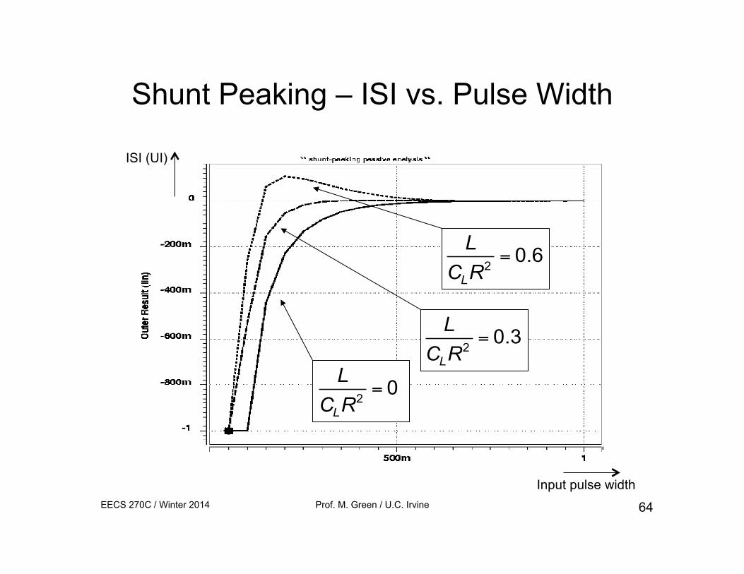
EECS 270C / Winter 2014 Prof. M. Green / U.C. Irvine 64
€
LCLR2
= 0
€
LCLR2
= 0.3
€
LCLR2
= 0.6
Shunt Peaking – ISI vs. Pulse Width
ISI (UI)
Input pulse width
EECS 270C / Winter 2014 Prof. M. Green / U.C. Irvine 65
Other Advantages of Shunt-Peaking
• CML load is passive & linear
• Can be shown to be very robust in the presence of parasitic series resistance and shunt capacitance ⇒ inductors can be placed far away from other CML circuit elements.
EECS 270C / Winter 2014 Prof. M. Green / U.C. Irvine 66
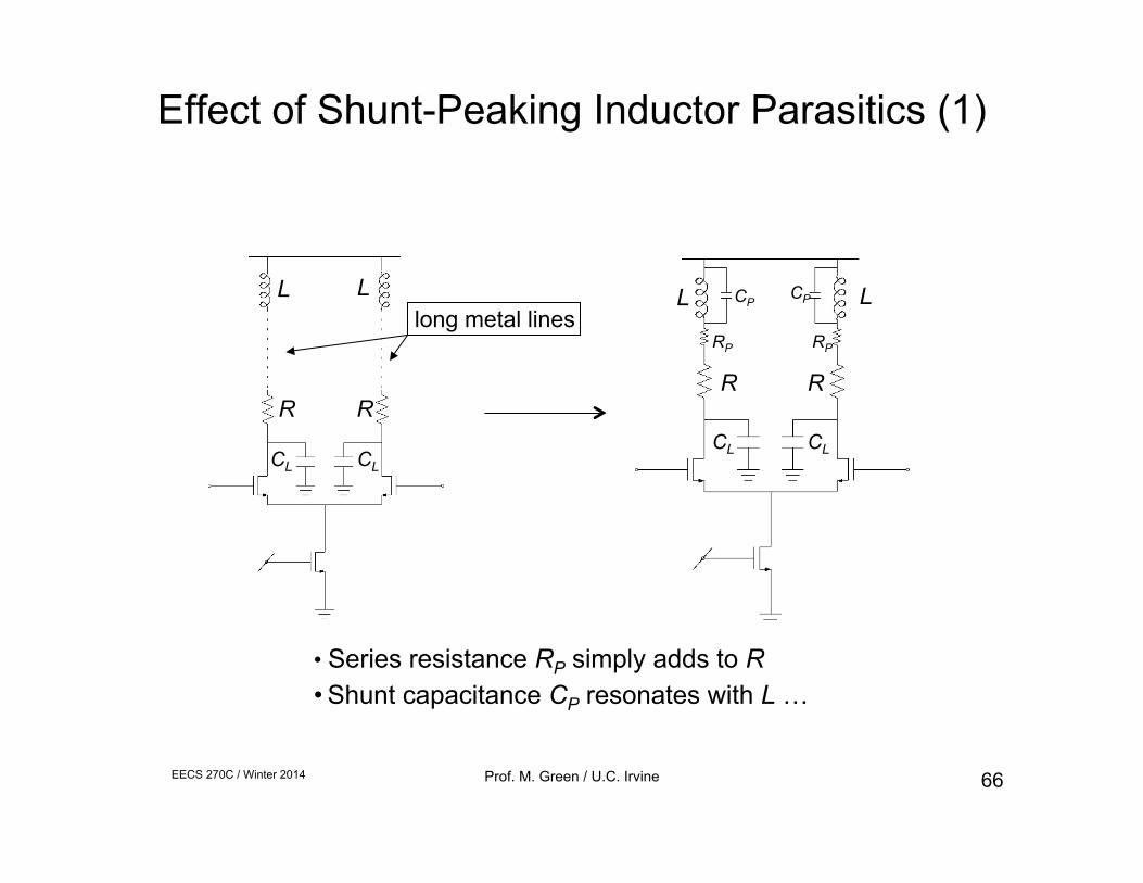
long metal lines
Effect of Shunt-Peaking Inductor Parasitics (1)
• Series resistance RP simply adds to R
• Shunt capacitance CP resonates with L …
L L
R R
CL CL CL CL
L L
R R
RP RP
CP CP
EECS 270C / Winter 2014 Prof. M. Green / U.C. Irvine 67
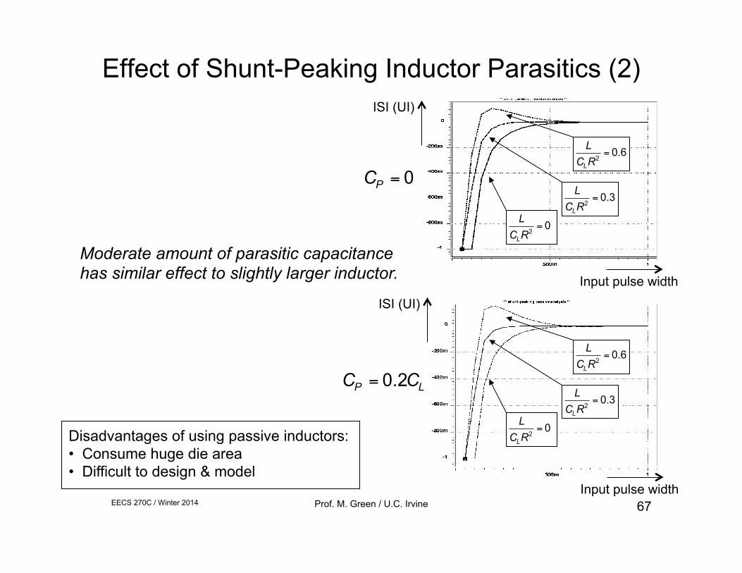
€
LCLR2
= 0
€
LCLR2
= 0.3
€
LCLR2
= 0.6
€
LCLR2
= 0
€
LCLR2
= 0.3
€
LCLR2
= 0.6
Moderate amount of parasitic capacitance has similar effect to slightly larger inductor.
Disadvantages of using passive inductors: • Consume huge die area • Difficult to design & model
Effect of Shunt-Peaking Inductor Parasitics (2)
€
CP = 0
€
CP = 0.2CL
Input pulse width
Input pulse width
ISI (UI)
ISI (UI)
EECS 270C / Winter 2014 Prof. M. Green / U.C. Irvine 68
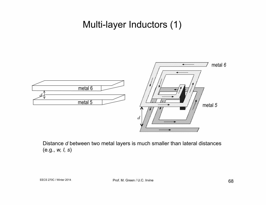
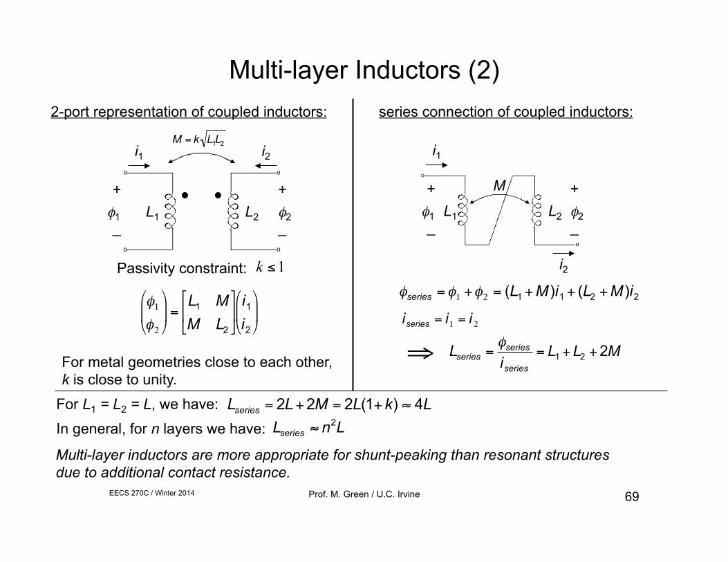
Multi-layer Inductors (1)
metal 6
metal 5 d
Distance d between two metal layers is much smaller than lateral distances (e.g., w, l, s)
metal 6
metal 5
d
EECS 270C / Winter 2014 Prof. M. Green / U.C. Irvine 69
€
φ1
φ2
#
$ %
&
' ( =
L1 MM L2
)
* +
,
- .
i1i2
#
$ % &
' (
L1 L2 φ1 φ2
+
_
+
_
i1 i2
2-port representation of coupled inductors:
€
M = k L1L2
Passivity constraint: 1≤k
For metal geometries close to each other, k is close to unity.
series connection of coupled inductors:
L1 L2
i1
i2
M
φ1
+
_ φ2
+
_
€
φseries =φ1 +φ2 = (L1 + M)i1 + (L2 + M)i2
€
iseries = i1 = i 2
€
Lseries =φseries
iseries
= L1 + L2 + 2M
€
⇒
For L1 = L2 = L, we have:
€
Lseries = 2L + 2M = 2L(1+ k) ≈ 4LIn general, for n layers we have:
€
Lseries ≈ n2L
Multi-layer inductors are more appropriate for shunt-peaking than resonant structures due to additional contact resistance.
Multi-layer Inductors (2)
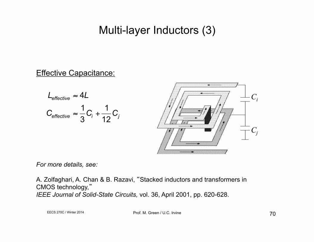
EECS 270C / Winter 2014 Prof. M. Green / U.C. Irvine 70
Ci
Cj
For more details, see: A. Zolfaghari, A. Chan & B. Razavi, “Stacked inductors and transformers in CMOS technology,” IEEE Journal of Solid-State Circuits, vol. 36, April 2001, pp. 620-628.
€
Leffective ≈ 4L
€
Ceffective ≈13
Ci +1
12Cj
Effective Capacitance:
Multi-layer Inductors (3)
EECS 270C / Winter 2014 Prof. M. Green / U.C. Irvine 71
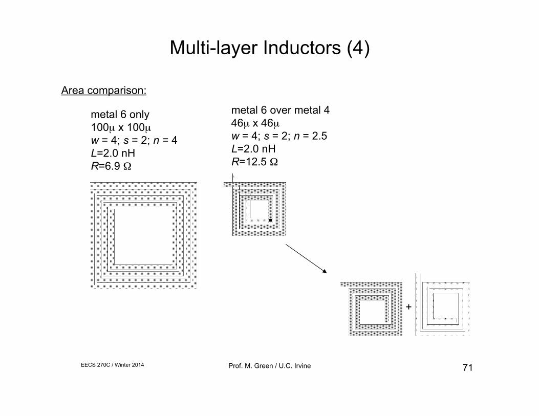
metal 6 only 100µ x 100µ w = 4; s = 2; n = 4 L=2.0 nH R=6.9 Ω
metal 6 over metal 4 46µ x 46µ w = 4; s = 2; n = 2.5 L=2.0 nH R=12.5 Ω
+
Multi-layer Inductors (4)
Area comparison:
EECS 270C / Winter 2014 Prof. M. Green / U.C. Irvine 72
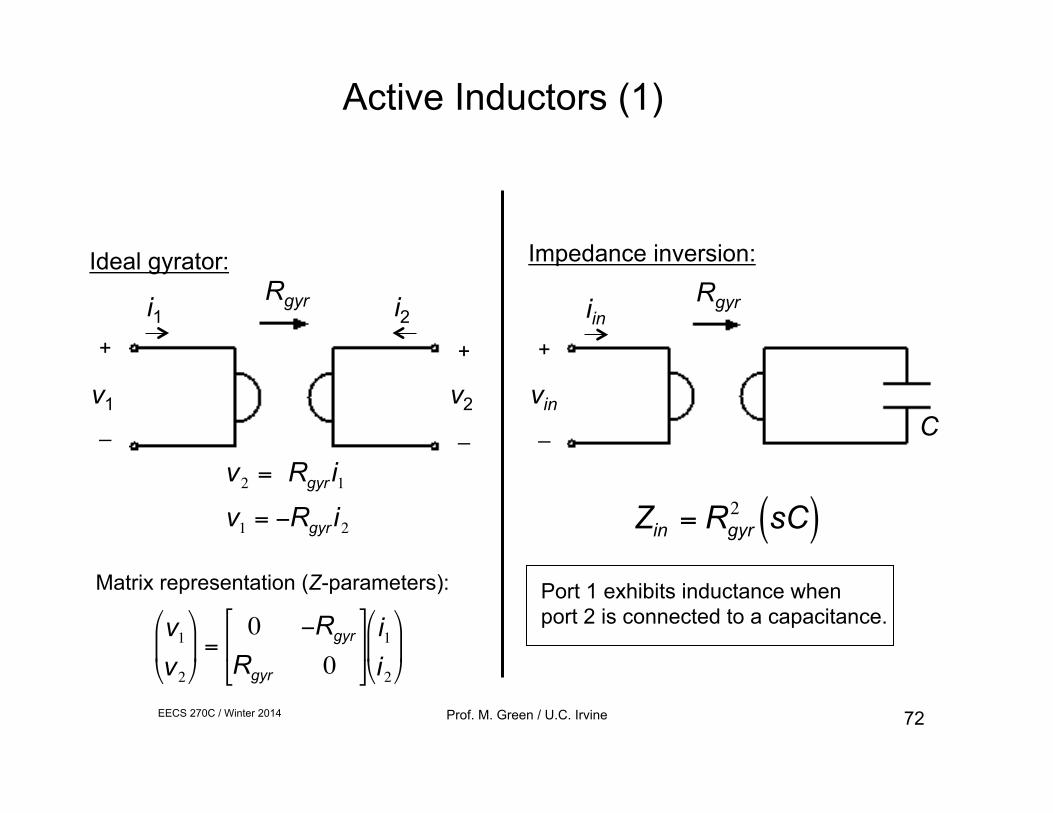
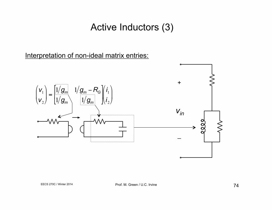
Active Inductors (1)
Rgyr
+
_ v1
i1
+
_
v2
i2
Ideal gyrator:
€
v2 = Rgyr i1v1 = −Rgyr i2
Impedance inversion:
Rgyr
+
_ vin
iin
C
€
Zin = Rgyr2 sC( )
Port 1 exhibits inductance when port 2 is connected to a capacitance.
€
v1v2
"
# $
%
& ' =
0 −Rgyr
Rgyr 0
)
* +
,
- .
i1i2
"
# $ %
& '
Matrix representation (Z-parameters):
EECS 270C / Winter 2014 Prof. M. Green / U.C. Irvine 73
Active Inductors (2)
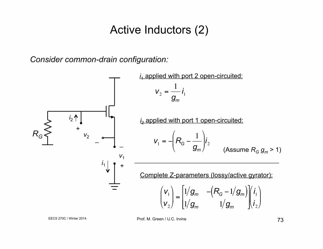
RG
+
_
v1 i1
+
_ v2
i2
i1 applied with port 2 open-circuited:
i2 applied with port 1 open-circuited:
€
v2 =1
gm
i1
€
v1 = − RG −1
gm
#
$ %
&
' ( i2
(Assume RG gm > 1)
€
v1v2
"
# $
%
& ' =
1 gm − RG −1 gm( )1 gm 1 gm
)
* + +
,
- . .
i1i2
"
# $ %
& '
Complete Z-parameters (lossy/active gyrator):
Consider common-drain configuration:
EECS 270C / Winter 2014 Prof. M. Green / U.C. Irvine 74
€
v1v2
"
# $
%
& ' =
1 gm 1 gm −RG
1 gm 1 gm
)
* +
,
- .
i1i2
"
# $ %
& '
+
_
vin
Active Inductors (3)
Interpretation of non-ideal matrix entries:
EECS 270C / Winter 2014 Prof. M. Green / U.C. Irvine 75
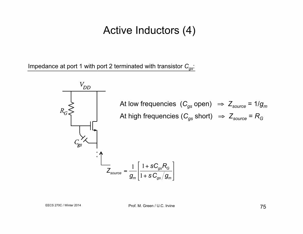
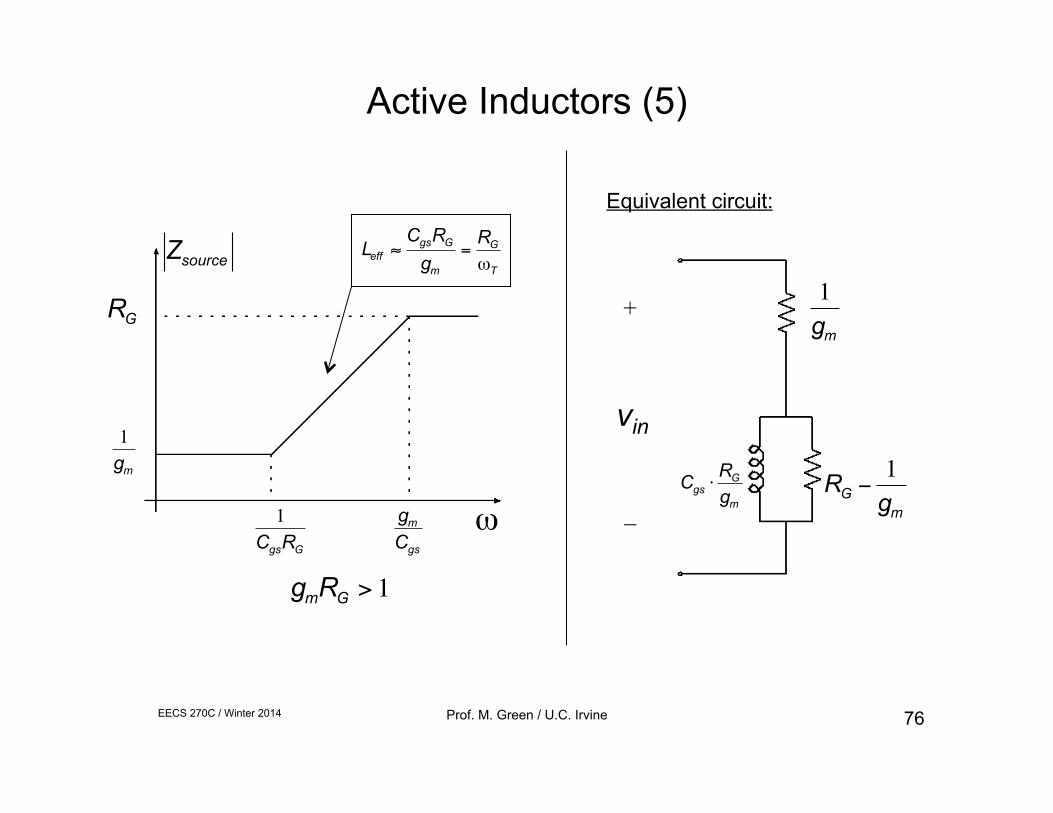
€
Zsource =1
gm
1+ sCgsRG
1+ sCgs gm
"
# $
%
& '
At low frequencies (Cgs open) ⇒ Zsource = 1/gm
At high frequencies (Cgs short) ⇒ Zsource = RG
Active Inductors (4)
Impedance at port 1 with port 2 terminated with transistor Cgs:
EECS 270C / Winter 2014 Prof. M. Green / U.C. Irvine 76
€
ω
€
gm
Cgs
€
1CgsRG
€
1gm
€
RG
€
Zsource
€
Leff ≈CgsRG
gm
=RG
ωT
€
gmRG > 1
Equivalent circuit:
+
_
vin
€
1gm
€
RG −1
gm
€
Cgs ⋅RG
gm
Active Inductors (5)
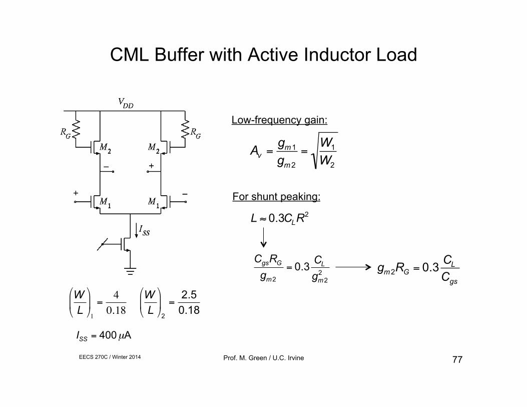
EECS 270C / Winter 2014 Prof. M. Green / U.C. Irvine 77
€
Av =gm 1
gm 2
=W1
W2
For shunt peaking:
€
L ≈ 0.3CLR2
€
CgsRG
gm2
= 0.3 CL
gm22
€
gm 2RG = 0.3 CL
Cgs
Low-frequency gain:
CML Buffer with Active Inductor Load
€
WL
"
# $
%
& ' 1
=40.18
€
WL
"
# $
%
& '
2
=2.50.18
€
ISS = 400µA
EECS 270C / Winter 2014 Prof. M. Green / U.C. Irvine 78
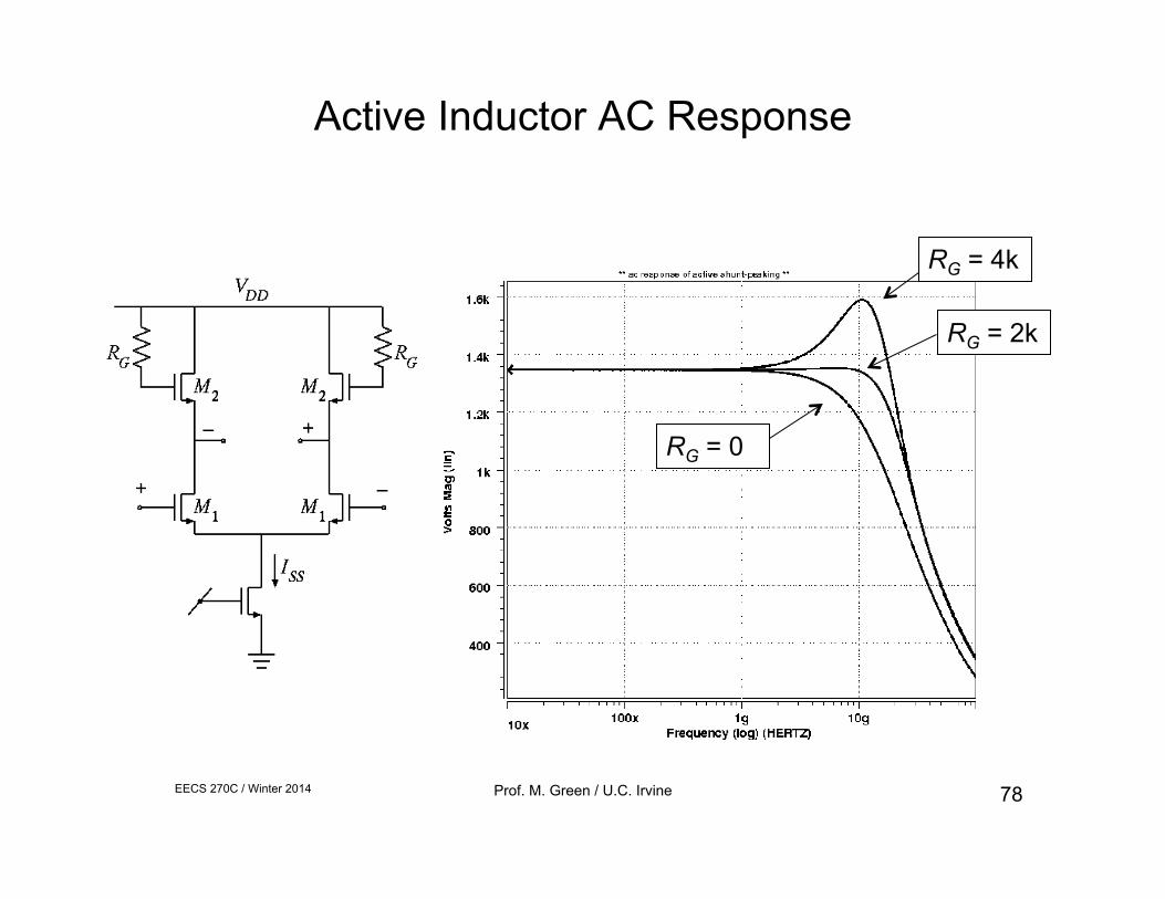
Active Inductor AC Response
RG = 4k
RG = 2k
RG = 0
EECS 270C / Winter 2014 Prof. M. Green / U.C. Irvine 79
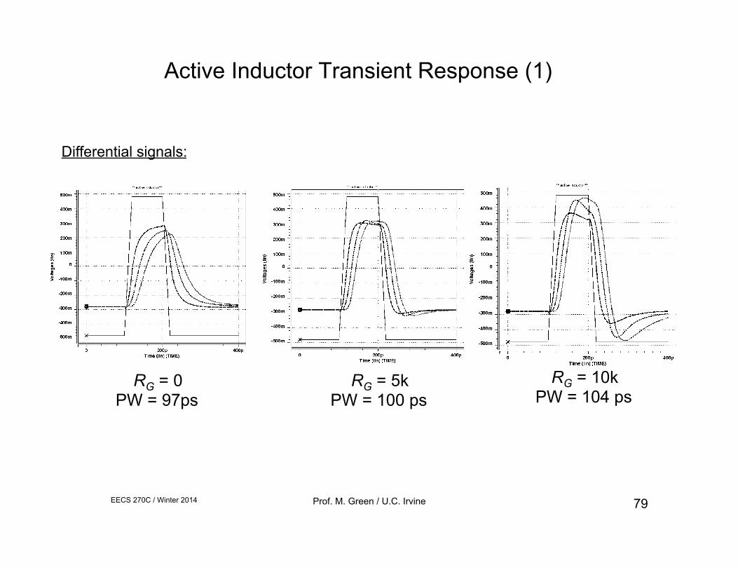
Active Inductor Transient Response (1)
RG = 0 PW = 97ps
RG = 5k PW = 100 ps
RG = 10k PW = 104 ps
Differential signals:
EECS 270C / Winter 2014 Prof. M. Green / U.C. Irvine 80
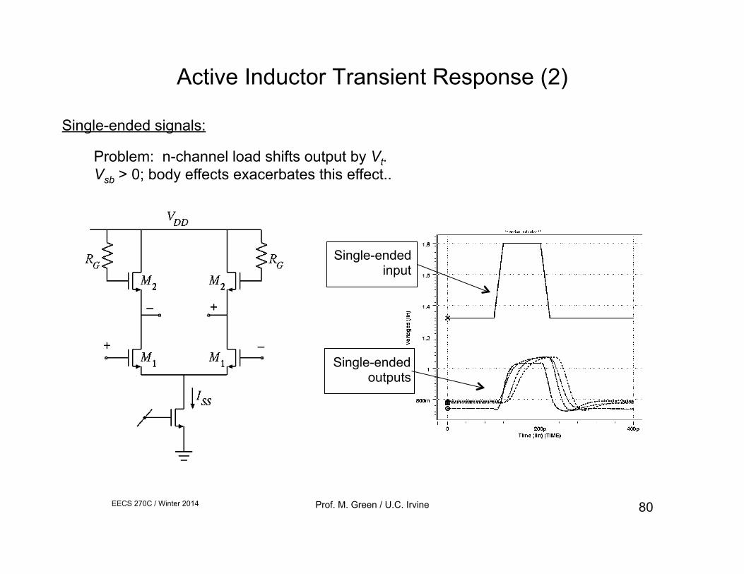
Active Inductor Transient Response (2)
Problem: n-channel load shifts output by Vt. Vsb > 0; body effects exacerbates this effect..
Single-ended input
Single-ended outputs
Single-ended signals:
EECS 270C / Winter 2014 Prof. M. Green / U.C. Irvine 81
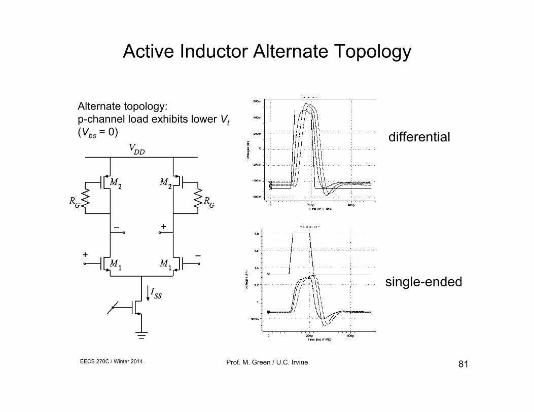
Alternate topology: p-channel load exhibits lower Vt (Vbs = 0)
Active Inductor Alternate Topology
differential
single-ended