advanced perspectives in the vapor-phase deposition of
TRANSCRIPT

Advanced Perspectives in the Vapor-
Phase Deposition of Multifunctional
Metal Oxide Nanomaterials
Dissertation
Daniela Bekermann


Advanced Perspectives in the Vapor-
Phase Deposition of Multifunctional
Metal Oxide Nanomaterials
Dissertation
zur Erlangung der Doktorwürde
der Fakultät für Chemie der Ruhr-Universität Bochum
vorgelegt von
M.Sc. Daniela Bekermann
Bochum, April 2012


This dissertation is based on the experimental work carried out during the period from
August 2008 to July 2011 under the supervision of Prof. Dr. R. A Fischer at the Chair of
Inorganic Chemistry II, Organometallics & Materials, Ruhr-University Bochum,
Germany.
Referees
Prof. Dr. Roland A. Fischer
Dr. Davide Barreca
Herewith I declare that I have written this thesis myself and without any other help or
sources which are not specifically and explicitly marked or named in this dissertation.
Furthermore, I declare that I have not applied to any other review procedure or submitted
this thesis in the same, similar or different form to another faculty or university as a
dissertation.
Daniela Bekermann.


Meinen Eltern - Dirk und Monika Bekermann


Wissenschaft:
„Die systematische Klassifizierung der Erfahrung.“ - Sinclair Lewis
„Die Voraussicht von Wiederholungen.“ - Antoine de Saint-Exupéry
„Ein erstklassiges Möbelstück für das Oberstübchen eines Mannes, der gesunden
Menschenverstand im Erdgeschoß hat.“ - Oliver Wendell Holmes sen.

Mein besonderer Dank gilt Prof. Dr. Roland Augustinus Fischer, für das
entgegengebrachte Vertrauen in meine Arbeit, die gewährten Freiheiten, und vor allem
für die Motivation und Perspektiven, die er mir in meiner Promotionszeit gegeben hat.

Acknowledgements
Prior to all, I want to thank my supervisors Prof. R. A. Fischer and Dr. D. Barreca, who,
by their complementary teaching and leading personalities, view of life and great
kindness, made it not only possible for me, to learn a great deal of chemistry and
materials science but also for life.
I also greatly acknowledge Prof. A. Devi and Dr. A. Gasparotto who always found the
time for scientific discussions, practical help and their great support in general.
Researchers who shared work, beers and spritz with me are overall Dr. M. Walawalkar,
Dott. M. Gavagnin and Dr. Q. Simon.
A big “thank you” is dedicated to S. Pankau for her support in administrative issues and
her positive spirit.
I want to thank all co-workers and collaboration partners who contributed to this work:
Prof. E. Comini and Prof. G. Sberveglieri for the cooperation in gas sensing
measurements
Dr. V. Gombac and Prof. P. Fornasiero for the photocatalytic H2 production
testings
Prof. U. Lavrenčič-Štangar for PSH and PCO characterizations
Prof. C. Sada for SIMS measurements
Dr. O. I. Lebedev, Dr. S. Turner and Prof. G. Van Tendeloo for TEM analyses
Dr. C. Maccato for the excellent FE-SEM measurements and Italian food
Dr. A. Ludwig who performed PL measurements with me
Dr. D. Rogalla and Dr. H.-W. Becker for performing and teaching RBS
K. Xu and M. Banerjee for zinc precursor supply
I want to thank all the members of the ACII group and the Padova group for the good
working atmosphere. Special thanks are dedicated to the former office 2/26, for an
unforgettable time at and outside the RUB, and their friendship.
For their continuous support and motivation during the last years, I want to thank my
family and Marco.
These research activities have received funding from
the European Community’s 7th
Framework Program (FP7/2007-2013, grant
agreement n° ENHANCE-238409).
Collaborative Research Centre (SFB) 558: Metal-substrate interactions in
heterogeneous catalysis.
I greatly acknowledge everybody who supported me, applying for the grants, namely
Prof. Dr. Roland A. Fischer, Dr. Davide Barreca, Prof. Anjana Devi, Dr. Mrinal
Walawalkar and Dr. Erik Bründermann.


Table of Contents
Table of Contents
1. Introduction 1 1. Introduction 1 2. Thesis Outline 4
1. Application Fields and Open Challenges 4 2. Methods and Materials 5 3. Outline 9
2. Vapor-phase Deposition Approaches: CVD, Sputtering
and Hybrid Routes 11 1. Abstract 11 2. Introduction 11 3. Thermal CVD 12 4. PECVD 13 5. Sputtering 15 6. “Hybrid” Approach: CVD + Sputtering 16 7. Zinc Precursor Chemistry 17 8. Cobalt Precursor Chemistry 21
3. Zinc Oxide Nanostructures 24
1. Abstract 24 2. Introduction 25 3. Thermal CVD of ZnO Nanostructures on Si(100) and Borosilicate Glass 28
1. Deposition Procedure 28 2. Morphology and Structure 29 3. Composition 34 4. Optical properties 37
4. PECVD of ZnO Nanostructures on Si(100) and Polycrystalline Al2O3 39 1. Deposition Procedure 39 2. Morphology and Structure 40
1. ZnO Nanorod Growth on Si(100) from 1 40 2. ZnO Nanorod Growth on Si(100) from 2 45 3. Summary: ZnO Nanorod Growth on Si(100) from 1 and 2 48 4. ZnO Nanorod Growth on Al2O3 from 1 and 2 50
3. Composition 53 4. Optical Properties 56 5. PSH and PCO Properties 57 6. Gas Sensing Properties 61
5. Conclusions 70
4. Co3O4 72
1. Abstract 72 2. Introduction 73 3. PECVD of Co3O4 on Mg(100) and MgAl2O4(100) 76

Table of Contents
1. Deposition Procedure 76 2. Morphology and Structure 77 3. Composition 80
4. PECVD of (F-)Co3O4 on Si(100) and Polycrystalline Al2O3 82 1. Deposition Procedure 82 2. Morphology and Structure 84 3. Composition 89 4. Optical Properties 92 5. Photocatalytic H2 Production 93 6. Gas Sensing Properties 98
5. Conclusions 103
5. Ag/ZnO 105
1. Abstract 105 2. Introduction 105 3. PECVD and Sputtering of Ag/ZnO on Si(100) and Polycrystalline Al2O3 107
1. Deposition Procedure 107 2. Morphology and Structure 108 3. Composition 114 4. Photocatalytic H2 Production 118 5. Gas Sensing Properties 121
4. Conclusions 122
6. Co3O4/ZnO 124
1. Abstract 124 2. Introduction 124 3. PECVD of Co3O4/ZnO on Si(100) and polycrystalline Al2O3 126
1. Deposition Procedure 126 2. Morphology and Structure 127 3. Composition 131 4. PH and PCO Properties 136 5. Gas Sensing Properties 138
4. Conclusions 143
7. Summary and Perspectives 145 8. Experimental 150
1. Synthesis and Characterization of Bis(ketoiminato)zinc (II) complexes (1 and 2) 150 1. Synthesis of 1 and 2 150 2. NMR of 1 and 2 151 3. Single Crystal X-ray Diffraction of 1 153 4. EI-MS of 1 and 2 154 5. Thermal Characterization of 1 and 2 154
2. Synthesis and Characterization of [Co(dpm)2] (3) and [Co(hfa)2·TMEDA] (4) 155

Table of Contents
1. Synthesis of 3 and 4 155 2. EI-MS of 3 and 4 156 3. Thermal Characterization of 3 and 4 158
3. Reactor Set-ups and Applied Deposition Parameters 158 1. CVD Reactor Set-up 158 2. Deposition Parameters for CVD of ZnO (3.3.1) 160 3. Plasma Reactor Set-up 160 4. Deposition Parameters for PECVD of ZnO (3.4.1) 162 5. Deposition Parameters for PECVD of Co3O4 (4.3.1 and 4.4.1) 163 6. Deposition Parameters for PECVD/Sputtering of Ag/ZnO (5.3.1) 163 7. Deposition Parameters for PECVD of Co3O4/ZnO (6.3.1) 164
4. Precursor Characterization Techniques 165 1. Elemental Analysis (EA) 165 2. Nuclear Magnetic Resonance Spectroscopy (NMR) 165 3. Single Crystal X-ray Diffraction 166 4. Electron Impact-Mass Spectrometry (EI-MS) 167 5. Thermogravimetry/Differential Thermal Analysis (TG/DTA) 168
5. Materials Characterization Techniques 168 1. Atomic Force Microscopy (AFM) 169 2. Scanning Electron Microscopy (SEM) 170 3. Energy Dispersive X-ray Spectroscopy (EDXS) 171 4. Rutherford Backscattering Spectroscopy (RBS) 171 5. X-ray Photoelectron Spectroscopy and Auger Electron Spectroscopy
(XPS/XE-AES) 172 6. Secondary Ion Mass Spectrometry (SIMS) 175 7. X-ray Diffraction (XRD) 176 8. Transmission Electron Microscopy (TEM) 177 9. Fourier Transform Infrared Spectroscopy (FT-IR) 180 10. Ultraviolet/Visible Light Spectroscopy (UV-Vis) 180 11. Photoluminescence Spectroscopy (PL) 181
6. Functional Characterization Techniques 182 1. Photo-induced Superhydrophilicity (PSH) 182 2. Photocatalytic Oxidation (PCO) 183 3. Photocatalytic H2 Production 185 4. Gas Sensing 187
9. Bibliography 191
Curriculum Vitae Publications and Conferences Schools and Workshops


List of Abbreviations
List of Abbreviations
1 [Zn{[(CH3OCH2CH2)N]C(CH3)=C(H)C(CH3)=O}2] 2 [Zn{[(CH3OCH2CH2CH2)N]C(CH3)=C(H)C(CH3)=O}2] 3 [Co(dpm)2] 4 [Co(hfa)2·TMEDA] 1D, 2D, 3D one dimensional, two dimensional, three dimensional
A
α Auger parameter, absorption coefficient A area, absorbance acac acetylacetonate AFM Atomic Force Microscopy at. atomic ALD Atomic Layer Deposition
B
β heating rate Β0 magnetic field BE binding energy Bu butyl nBu n-butyl tBu tert-butyl
C
CVD Chemical Vapor Deposition Cp cyclopentadienyl
D
d distance between crystal planes, diameter, crystallite size DEA N,N’-diethylethylenediamine DEZ diethylzinc DMAEH 2-dimethylaminoethanol DMAPH dimethylamino-2-propanol DMZ dimethylzinc dpm 2,2,6,6-tetramethyl-3,5-heptanedionate DTA Differential Thermal Analysis
E
e- electron

List of Abbreviations
E energy EC conduction band EF Fermi level Eg band gap EV valence band EA Elemental Analysis EDXS Energy Dispersive X-ray Spectroscopy EELS Electron Energy Loss Spectroscopy EI-MS Electron Impact Mass Spectrometry Et ethyl
F
FE-SEM Field Emission SEM FT-IR Fourier Transform Infrared Spectroscopy FWHM full width at half-maximum
G
γ magnetogyric constant G conductance GB grain boundary GC Gas Chromatography GIXRD Glancing Incidence XRD GR growth rate
H
h Planck constant h+ hole HAADF high angle annular dark field HEC hydroxyethyl-cellulose hfa 1,1,1,5,5,5-hexafluoro-2,4-pentanedionate HR-TEM high resolution-TEM HOTPA hydroxyterephthalic acid HPLC-FLD High Performance Liquid Chromatography with Fluorescence Detection
I
I Intensity JCPDS Joint Committee on Powder Diffraction Standards IR infrared
K
k rate constant KE kinetic energy

List of Abbreviations
L
λ wavelength L ligand Ld Debye length
M
m mass µ magnetic moment Me methyl MBE Molecular Beam Epitaxy MFC mass flow controller m.p. melting point
N
n integer number ν frequency NP nanoparticle NaTPA sodium terephthalate NMR Nuclear Magnetic Resonance Spectroscopy NR nanorod
O
Oi interstitial oxygen
P
p pressure P power PC photocatalysis PCO photocatalytic oxidation PE primary electron PECVD Plasma Enhanced CVD Ph phenyl PL Photoluminescence (Spectroscopy) PLD Pulsed Laser Deposition Pr propyl iPr iso-propyl PSH photo-induced superhydrophilicity θ generic angle
Q
Φ work function

List of Abbreviations
Q Selectivity
R
R resistance RBS Rutherford Backscattering Spectroscopy RF radio frequency RMS root mean square RT room temperature
S
S atomic sensitivity factor, sensor response σ electron shielding, chemical shift SC semiconductor SE secondary electron SEM Scanning Electron Microscopy SF stacking fault SIMS Secondary Ion Mass Spectrometry S/N signal-to-noise (ratio) SPR Surface Plasmon Resonance STEM Scanning Transmission Electron Microscopy
T
t time, thickness T temperature, transmittance Tvap evaporation temperature THF tetrahydrofuran THP tetrahydropyran TEM Transmission Electron Microscopy tetraglyme Me(OCH2CH2)4OMe TG Thermogravimetry TMEDA N,N,N’,N’-tetramethylethylenediamine tmp 2,2,6,6-tetramethylpiperidino TMP turbo molecular pump TMS trimethylsilyl group TPA terephthalic acid tta 2-theonyltrifluoroacetonate
U
UV ultraviolet
V
VO oxygen vacancy

List of Abbreviations
VZn zinc vacancy Vis visible
W
ω Larmor frequency, resonance frequency WCA water contact angle WT working temperature
X
x molar fraction XE-AES X-ray Excited Auger Electron Spectroscopy XPS X-ray Photoelectron Spectroscopy XRD X-ray Diffraction
Z
z ion charge Zni interstitial zinc


1. Introduction
1
1. Introduction
1.1 Introduction
The assignment “nano” is usually given to materials whose structural features exhibit at
least one dimension in the sub-100-nanometer range, consisting of a few hundred of
thousands of atoms or molecules. [Cademartiri-2009, Elias-2010, Herron-1998, Rao-
2004] Size (i.e. the scale threshold) however, is not everything, since even nanomaterials
physico-chemical properties vary significantly from those of the bulk counterparts, [Rao-
2004, Herron-1998] resulting in unique functional characteristics for a variety of
applications. [Barreca-2011-A, Barreca-2011-B, Bekermann-2010-A, Choy-2003, Curri-
2010, Gasparotto-2011, Rao-2004, Tricoli-2009, Trindade-2001, Wang-2011-A, Xia-
2003] Nanosystem design and fabrication, especially for metal oxide based materials, are
generally performed to attain the following main attributes:
(i) A high surface area, usually related to an enhanced reactivity. This feature is of
outermost importance in surface sensitive processes, such as catalysis, photocatalysis and
gas sensing. [Barreca-2011-B, Lee-2009-A, Özgür-2005, Shifu-2009, Si-2006, Trindade-
2001]
(ii) Quantum confinement effects, mainly exploited for photo-activated processes and
sensing, since variations in nanoparticle sizes result in significant alterations of the charge
carrier behaviour. [Barreca-2011-B, Curri-2010, Gong-2000, Lee-2009-A, Özgür-2005,
Rao-2004, Trindade-2001, Zhuge-2010]
(iii) Control of surface active sites and defects incorporation, a useful mean to tailor the
system chemical, physical and functional properties. [Dong-2008, Du-2008, Fu-2007-A,
Rao-2004]
As a matter of fact, nano-physics and nano-chemistry are governed by many factors, like
material composition, structure and morphological organization, [Cademartiri-2009,
Elias-2010, Rao-2004] and their control promises new perspectives both in science and in
technology. [Chithrani-2009, Elias-2010, Hu-2008, Özgür-2005, Rao-2004] As a
consequence, various types of nanostructures, supported or unsupported, ranging from 0D
to 2D materials (see figure 1.1), have been synthesized and thoroughly investigated.
0D nanocrystals have reduced sizes (below 100 nm) in all three dimensions and their size
and shape determine their functionality. For example, peculiar optical properties like
Surface Plasmon Resonance are directly determined by the nanoparticle (NP) shape,

1. Introduction
2
dimensions and mutual interactions. [Seyed-Razavi-2010] In addition, NP size and
exposed facets are known to affect the system catalytic activity and selectivity. [Seyed-
Razavi-2010] Furthermore, gas sensing performances of metal oxide nanomaterials can
be greatly enhanced when one of the characteristics becomes comparable or smaller than
the Debye length1. [Lee-2009-B, Barreca-2010-A]
2D nanostructures
(thin films/coatings.. )
Hierarchal structuresSupported structuresCrystallite structures
0D nanoparticles/crystallites
1D nanostructures (rods/wires..)
Figure 1.1: Sketch of various types of nanosystems.
In the past years, increasing interest was dedicated to the development and investigation
of 1D nanostructures due to their various outstanding properties. [Comini-2009-A, Özgür-
2005, Prades-2009] For instance, ZnO nanowires showed superior photo-detection
performances compared to 2D ZnO thin films. [Prades-2008] This result was attributed to
various factors, including a prolonged lifetime of the photo-generated carriers and an
improved trapping of the incident photons in comparison to ZnO thin films. [Prades-
2008] ZnO NR arrays have also received considerable attention for their advanced photo-
activated functions, regarding, in particular, photo-induced superhydrophilicity (PSH), for
1 The Debye length is the scale over which significant charge separation is probable. In the case of
semiconductors, the electrical conductivity processes are dependent on this parameter, being LD = [(k T ) /
(q2 n)]
1/2, where k is the Boltzmann constant, T the temperature, the dielectric constant, q the electron
charge and n the carrier concentration. [Comini-2009-A, Mizsei-1995, Ogawa-1982]

1. Introduction
3
self-cleaning applications, and photocatalysis (PC), for pollutant degradation. [Badre-
2009, Liu-2009-A, Sun-2005, Wan-2005]
2D nanodeposits, such as supported nanostructure and thin films, are also widely used as
functional coatings, from corrosion protection up to microelectronics and photovoltaic
applications. [Choy-2003, Hsieh-2008]
Apart from 0D particles, 1D materials and 2D films, more complex systems, like
hierarchal structures (figure 1.1), have gained growing attention for the direct
dependence of their properties on spatial organization. [Lee-2009-A, Morkoç-2009] For
instance, it was demonstrated that the use of these assemblies can be beneficial for gas
sensing applications, by providing a high surface area and nanosize effects along with
effective gas diffusion toward the entire sensing surfaces via the porous structures. [Lee-
2009-A]
Increasing efforts have also been focused on the preparation of nanoheterostructures.
[Bekermann-2012, Higashiwaki-2009, Lee-2009-A, Meyyappan-2009, Na-2011, Simon-
2011] In fact, the combination of the advantages of nanoscale materials combined with
the synergistic coupling of the component features, paves the way to the development of
systems endowed with unprecedented properties. [Fu-2007-A, Kim-2005-A, Gao-2005] In
this context, among the various systems, ZnO-Co3O4 systems have received attention for
their magnetic, [Martín-González-2008] catalytic, [Llorca-2008, Rubio-Marcos-2010]
photocatalytic [Kanjwal-2011] and gas sensing properties. [Na-2011] In addition, two
main aspects to be considered in heterostructures are the formations of Schottky and p/n
junctions, occuring at metal/semiconductor (SC) and p/n-type SC interfaces, respectively.
These phenomena typically result in rectifiying effects and enhanced electron/hole (e-/h
+)
separation, with a favourable impact especially on photocatalytic and sensing
performances. [Bekermann-2012, Kim-2005-A, Na-2011, Shifu-2009, Simon-2011]
Particularly in the nanoregime, interactions resulting from the contact of two components
are of great importance, since a high spatial density of interfaces is generated when the
components are brought in intimate contact. [Fu-2007-A]
Basing on the above considerations, the design of multifunctional oxide nanomaterials
requires the development of proper synthetic procedures, enabling a fine control of their
chemico-physical features, and characterized by a low environmental impact.

1. Introduction
4
1.2 Thesis Outline
1.2.1 Application Fields and Open Challenges
In this thesis, the development of multifunctional nanomaterials (based on ZnO, Co3O4,
Ag/ZnO and Co3O4/ZnO) for applications in the following main fields has been
addressed:
(1) solid state gas sensing;
(2) PSH and photocatalytic oxidation (PCO) properties for pollutant degradation;
(3) photocatalytic H2 production, starting from aqueous solutions of suitable oxygenates,
under both UV-Vis and Vis light irradiation.
The interest in (1) is motivated by the increasing concern regarding the effects of
pollution on health and safety, stimulating remarkable efforts toward real-time
environmental monitoring. [Barreca-2011-C, Comini-2009-A, Comini-2010, Li-2009-A,
Prades-2009] Since the performances of solid state gas sensors are directly dependent on
the surface and morphology of the active material, [Basu-2008, Lupan-2010] an
interesting challenge concerns the controlled fabrication of oxide-based low-dimensional
nanomaterials with a high surface-to-volume ratio, possessing electrical properties very
sensitive to surface-adsorbed species. [Barreca-2011-C, Comini-2010, Li-2009-A] In
particular, efforts have been aimed at achieving improved sensing performances by a
careful control of the material structure, composition and spatial organization.
Regarding (2), the photo-activity of the synthesized oxide nanostructures has been studied
using water contact angle (WCA) measurements and photocatalytic oxidation of
terephthalic acid (TPA). PSH properties, meaning photo-activated hydrophobic-to-
superhydrophilic conversion, can be investigated by monitoring the evolution of the
WCA of a water droplet on the nanomaterial surface as a function of the UV irradiation
time, as done in this work. [Bekermann-2010-A] The term “superhydrophilicity” is used if
the WCA << 90°. The self-cleaning activity of the synthesized materials upon photo-
activation was investigated via a highly sensitive PCO method based on the monitoring of
a TPA oxidation product, namely hydroxyterephthalic acid (HOTPA). [Černigoj-2010]
For both PSH and PCO the requirement is the generation and separation of electrons and
holes upon light absorption by the SC material. In the case of PSH, the activation
promotes the dissociative chemisorption of H2O and thus hydrophilic behaviour.
[Fujishima-2000] The mechanism generally accepted for PCO involves the photo-
generation of highly reactive radicals, which can subsequently decompose organic

1. Introduction
5
compounds. [Bekermann-2010-A, Fujishima-2000] Overall, PSH and PCO properties of
SC nanostructures open up attractive perspectives for the eventual development of
stimuli-responsive systems. [Badre-2009, Bekermann-2010-A, Liu-2009-A, Sun-2005,
Wan-2005]
As concerns (3), the widespread interest in sustainable H2 generation is due to its high
demand not only in industrial processes, [Armaroli-2011, Reisner-2011] but more
importantly as an energy vector, due to the depletion of fossil sources. [Ni-2007-A,
Cargnello-2011] Up to date, one of the most sustainable routes, the generation of H2 from
photocatalytic water-splitting, has been widely investigated but remains extremely
challenging, especially in terms of the process efficiency. [Cargnello-2011] In a different
way, H2 production by photoreforming of biomasses, such as alcohols, is much less
investigated and offers an attractive alternative. [Navarro-2009, Fu-2008] Photo-
reforming is based on the oxidation of the feedstock to CO2 under the generation of H2
(reaction 1.1), catalyzed by a suitable photo-activated semiconductor material.
CnHmOk + (2n − k) H2O → n CO2 + (2n + m/2 − k) H2 (reaction 1.1)
In this work, water/alcohol (methanol or ethanol) mixtures have been used for
preliminary tests. [Montini-2011] In order to fully exploit the potential of this process, it
is of paramount importance to develop catalytic systems that are not affected by leaching
or poisoning phenomena and possess a high efficiency, in particular upon Vis activation.
Accordingly, herein novel nanosystems for photocatalytic H2 production have been
developed and tested, namely pure and F-doped Co3O4 and Ag/ZnO nanocomposites.
1.2.2. Methods and Materials
Deposition methods
In the present thesis, the main attention is devoted to exploiting vapor-phase processes,
namely Chemical Vapor Deposition (CVD), both thermal and Plasma Enhanced
(PECVD), and sputtering, and their synergistic combination, to obtain specific kinds of
functional nanomaterials. CVD relies on the activation of gaseous reactants near or on a
substrate surface, leading to the synthesis of the target material by chemical reaction.
[Choy-2003, Pierson-1999] The activation can occur thermally, by heating the substrate,
or, in the case of PECVD, by cold reactive plasma (see chapter 2). The main advantages

1. Introduction
6
of the CVD technique are flexibility, the possibility of large-scale production, moderate
process temperatures, conformal step coverage and the ability to grow various
nanostructures by suitable choice of the experimental parameters. [Choy-2003, Pierson-
1999, Tricoli-2009] Due to the unique plasma activation, PECVD additionally offers
more degrees of freedom in the processing conditions and the use of lower substrate
temperatures compared to other vapor-phase methods. [Choy-2003, Gasparotto-2011,
Zheng-2010-A] The precursors used in CVD processes play a key role, since their
decomposition leads directly to the formation of the desired material. [Choy-2003,
McElwee-White-2006, Pierson-1999] To this regard, in this work, efforts were further
devoted to the synthesis and characterization of suitable Zn and Co precursors.
As regards sputtering, the source materials (here Ag) is placed in vacuum and exposed to
a plasma, resulting in the ejection of target atoms and subsequent deposition of the
reactive particles on the substrate (chapter 2). Due to the high infiltration power and low
temperatures required (down to the room one), sputtering is a valuable technique for the
synthesis of nanocomposites. [Barreca-2008-A, Simon-2011]
The potential of these techniques has been successfully used for the development of ZnO
and Co3O4 nanomaterials, for their controlled modifications, and for the ultimate
preparation of ZnO and Co3O4 heterostructures.
ZnO
ZnO, a biosafe n-type semiconductor with a wide direct band gap (Eg = 3.4 eV) and a
large exciton binding energy (60 meV), [Bekermann-2010-B, Morkoç-2009] can be
grown in an extremely wide range of morphologies [Calestani-2010, Fu-2007-B, Kuang-
2005, Morkoç-2009, Wang-2008-A, Zhou-2006] and enabled the development of several
ZnO-based systems for a variety of advanced applications. [Kuang-2005, Wang-2005-A]
ZnO NR arrays have received considerable attention for their advanced photo-activated
functions, in particular PSH and PC properties, [Badre-2009, Bekermann-2010-A, Liu-
2009-A, Sun-2005, Wan-2005] and for gas sensing of various analytes. [Barreca-2010-A,
Kang-2006, Özgür-2005, Öztürk-2011] In spite of the numerous works on ZnO, the
rational design of 1D ZnO nanosystems still deserves further investigations, in order to
understand fundamental phenomena in low-dimensional structures and to implement
innovative multifunctional materials. [Bekermann-2010-B, Scalisi-2008, Wang-2008-A]

1. Introduction
7
Co3O4
Subsequently, the attention has been devoted to Co3O4, a mixed valence p-type
semiconductor with a spinel structure, particularly interesting due to its high catalytic
activity, making it an attractive candidate for H2 production and gas sensing. [Barreca-
2010-B, Barreca-2011-C, Choi-2010, Ikeda-1998, Ikeda-1999] Beyond the control of the
system nano-organization, efforts were dedicated to fluorine-doping of the obtained
Co3O4 nanosystems. Fluorine-doping has been reported to improve functional
performances of n-type semiconductors and never been investigated before for Co3O4
nanomaterials. [Barreca-2011-C, Chen-2010-A, Liu-2010, Pawar-2008, Zhao-2010]
Indeed, the controlled introduction of fluorine has been revealed to be a key tool in order
to achieve superior functional performances.
Ag/ZnO
Beyond the study of columnar ZnO arrays, the attention has also been focused on
Ag/ZnO composites, characterized by controlled distribution of metal nanoparticels.
Photocatalytic and gas sensing properties can be improved by the synergistic combination
of nanostructured ZnO with metal NPs, which, beside their inherent catalytic activity,
promote an enhancement of charge carrier separation due to Schottky barriers at the
metal/oxide interface. [Fu-2007-A, Zeng-2008, Barreca-2011-A]. Among the different
metals, silver has a great potential to enhance ZnO photo-activity [Height-2006, Lu-2008,
Tan-2008, Lin-2009] and gas sensing performances, [Comini-2009-A, Basu-2009] but
only a few reports have been focused on Ag/ZnO systems for these applications up to
date. [Xiang-2010]
Co3O4/ZnO
Finally, on the basis of previous results, the last part of the activities has been
concentrated on Co3O4/ZnO nanosystems, in order to develop gas sensors and photo-
active materials with improved functional performances. [Na-2011, Shifu-2009] To this
regard, apart from the synergistic combination of the inherent properties of the single-
phase materials and nanoscale effects, the formation of p/n junction at interfaces enables

1. Introduction
8
an enhanced separation of photo-generated carriers and more extended depletion layers in
sensing process. [Zhuge-2010, Hsieh-2008, Shifu-2009, Kim-2005-A, Na-2011] However,
only very limited literature on the formation and functionality of Co3O4/ZnO
nanoheterostructures is available so far.
Characterization Techniques
The composition and molecular structure of the developed precursors has been
determined by Elemental Analysis (EA), Nuclear Magnetic Resonance Spectroscopy
(NMR) and Single Crystal X-ray Diffraction (XRD). In addition, Electron Impact Mass
Spectrometry (EI-MS) and Thermogravimetry/Differential Thermal Analysis (TG/DTA)
were performed in order to study the fragmentation and thermal properties of the zinc and
cobalt precursor molecules.
Subsequently, a detailed compositional, morphological and microstructural and optical
characterization of the obtained nanosystems has been carried out by means of a multi-
technique approach. Complementary bulk and surface investigation techniques allowed
obtaining a thorough and detailed picture of the system properties and their interrelations
with the synthesis conditions. This activity, representing a considerable part of the thesis,
has been performed by means of the following techniques:
(I) Field Emission Scanning Electron Microscopy (FE-SEM) and Atomic Force
Microscopy (AFM), for the study of the nanosystems morphology and its interrelations
with the synthesis conditions.
(II) Energy Dispersive X-ray Spectroscopy (EDXS) and Rutherford Backscattering
Spectroscopy (RBS) to obtain compositional information on the investigated
nanomaterials. To collect further quantitative data on the system surface and in-depth
chemical composition, X-ray Photoelectron Spectroscopy (XPS), X-ray Excited Auger
Electron Spectroscopy (XE-AES) and Secondary Ion Mass Spectrometry (SIMS) were
utilized.
(III) X-ray Diffraction (XRD) and Transmission Electron Microscopy (TEM) to achieve a
thorough insight into the systems microstructural features.
(IV) Fourier Transform Infrared Spectroscopy (FT-IR), Ultraviolet/Visible Light
Spectroscopy (UV-Vis) and Photoluminescence Spectroscopy (PL) to obtain further
information on the material composition and optical properties.

1. Introduction
9
1.2.3 Outline
In this thesis, the development of multifunctional ZnO, Co3O4, Ag/ZnO and Co3O4/ZnO
nanomaterials is pursued by bottom-up techniques, namely CVD, PECVD, sputtering and
their combinations (figure 1.2). Indeed, the results and discussions part will illustrate that
the adopted strategies open up attractive perspectives for the design of nanostructured
materials with specific applicative aims.
Figure 1.2: Schematic representation of the functional nanomaterials presented in this
work.
In particular, chapter 2 provides the basic principles and advantages for the CVD and
sputtering processes, highlighting their role for the growth of nanostructures and
composites. Furthermore, the choice of the zinc and cobalt CVD precursors used in this
thesis is discussed in the context of the state of the art state in Zn and Co precursor
chemistry.
Chapter 3 deals with the CVD and PECVD of ZnO nanodeposits. The application of
suitable metal organic Zn precursors, [Zn{[(CH2)xOCH3]NC(CH3)=C(H)C(CH3)=O}2] (1:
x = 2; 2: x = 3), led to the obtainment of pure ZnO nanomaterials, whose morphology,
structure and composition have been studied as a function of the adopted process
parameters. The 1D nanorod (NR) arrays, derived from PECVD, were investigated
regarding their activity in PSH and PCO and sensing properties of various analytes
(CH3CH2OH, CH3COCH3, CO, H2, CH4, O3 and NO2).

1. Introduction
10
In chapter 4, the PECVD of Co3O4 nanosystems from the metal organic sources,
[Co(dpm)2] (3) (dpm = 2,2,6,6-tetramethyl-3,5-heptanedionate) and [Co(hfa)2·TMEDA]
(4) (hfa = 1,1,1,5,5,5-hexafluoro-2,4-pentanedionate; TMEDA = N,N,N’,N’-
tetramethylethylenediamine), is described. In PECVD, the use of 3 yielded pure Co3O4
nanodeposits, whereas precursor 4 enabled in-situ fluorine-doping of the spinel by
generation of fluorine radicals in the reactive plasmas. The material features were
characterized by a combined analyses technique and the resulting impact on the
functional performances in the photocatalytic H2 production and detection of ethanol and
acetone were studied.
Ag/ZnO nanoheterostructures (chapter 5) have been obtained by a hybrid approach,
using PECVD of ZnO and sputtering of Ag nanoparticles. The influence of the silver
amount and distribution, controlled by the processing parameters, on the functionality in
H2 photocatalytic generation and sensing has been investigated in detail.
In chapter 6, the development of Co3O4/ZnO nanocomposites of varying Co3O4 amount
via a two-step PECVD is shown. A multi-characterization technique has been adopted to
investigate the morphological, structural and compositional features of the composite
materials. Preliminary tests, studying their PSH and PCO properties were performed, and
their application in the gas-phase detection of acetone, ethanol and nitrogen dioxide is
also discussed.
Summary and perspectives of the present work are presented in chapter 7.
In the experimental section (chapter 8), the synthesis and characterization of the applied
precursor compounds (1, 2, 3, and 4) is briefly discussed. The used reactor set-ups are
also described, and an overview of the applied deposition parameters for the
nanomaterials presented in chapters 3 – 6 is provided. Finally, the analytic methods,
carried out for the precursor and nanodeposit characterization, and for the functional
characterization, are described.

2. Vapor-phase Deposition Approaches: CVD, Sputtering and Hybrid Routes
11
2. Vapor-phase Deposition Approaches: CVD, Sputtering and Hybrid
Routes
2.1 Abstract
In the present chapter, first, the general motivation for the development of nanomaterials
by vapor-phase deposition approaches is presented (2.2). In the following paragraphs, the
basic principles and advantages of the adopted techniques, CVD (2.3), PECVD (2.4),
sputtering (2.5) and hybrid approaches (2.6), are briefly described, highlighting their
importance for the growth of the oxide nanomaterials developed in the present thesis.
Paragraphs 2.7 and 2.8 give a brief overview of the state of the art in zinc and cobalt
precursor chemistry, respectively, pointing out the benefits of the precursors used in this
thesis.
2.2 Introduction
Basing on the main applicative challenges in nanomaterial synthesis discussed in chapter
1, versatile low-temperature processes are required to control the system composition,
nanostructure and morphological organization. The tailoring of such features is essential
in order to exploit the nanosystem properties that underpin advanced applications.
[Gasparotto-2011, Morkoç-2009] Various nanomaterials preparation methods and
properties are extensively reviewed in numerous articles, reports and books, ranging from
nanopowders by precipitation, to supported 1D materials by template routes, up to various
kinds of hierarchical nanostructures. [Curri-2010, Gasparotto-2011, Rao-2004, Wang-
2008-B, Wang-2011-A, Xia-2003, Zhai-2010]
At variance with top-down approaches, like etching, lithography or ion beam milling, that
often require harsh conditions and do not enable a high control on the system nano-
organization, bottom-up approaches, based on the controlled assembly of
atomic/molecular units, can be considered a more amenable choice. [Comini-2009-A,
Elias-2010] As a matter of facts, CVD and sputtering processes belong to this category.
The general benefits of CVD among other synthesis techniques are its conformal
deposition also on 3D complex architectures and ability to produce a large variety of pure
nanostructures with controlled crystallinity. [Becker-2009, Choy-2003, Pierson-1999,
Tricoli-2009] Compared to wet chemical approaches, CVD methods are favorable to

2. Vapor-phase Deposition Approaches: CVD, Sputtering and Hybrid Routes
12
attain higher system purity and to avoid drying steps. Furthermore, in contrast to physical
vapor deposition processes, they have not the drawback of line-of-sight deposition. The
deposition rates achieved by CVD are relatively high and no ultrahigh vacuum is
necessary. CVD technology is very versatile in the choice of various physical and
chemical experimental parameters, allowing a fine-tuning of the eventual system
properties. [Choy-2003, Dong-2008, Liang-2011, Pierson-1999, Seshan-2002]
The main drawback of relatively high substrate temperatures, often ascribed to the
classical thermal CVD, can be easily overcome by a proper choice of the process
activation mode. [Barreca-2011-D, Gangil-2007, Higashiwaki-2009, Pierson-1999,
Zheng-2010-A] In this way, depositions of various materials also on heat-sensitive
substrates are possible.
Among physical techniques, sputtering, Molecular Beam Epitaxy (MBE), Pulsed Laser
Deposition (PLD) and thermal evaporation have been widely used to produce epitaxial
materials with well controlled stoichiometry and doping level. [Fu-2007-A] Yet, thermal
evaporation often requires extremely high vaporization temperatures, [Katti-2003, Xu-
2007] and MBE/PLD involve high energy dissipation, being thus not amenable for
practical applications. [Pierson-1999, Si-2006] In contrast, sputtering can be carried out at
low temperatures, even down to the room one, [Barreca-2011-A, Hsieh-2011, Simon-
2011] and requires a less complex instrumental apparatus. [Pierson-1999]
2.3 Thermal CVD
In the “classical” and up to date mainly applied thermal CVD, the reagents (metal organic
precursors, compounds, reactive gases) are vaporized, transported into the reaction
chamber and thermally activated/decomposed on a hot substrate surface to form the target
material by chemical reaction. [Choy-2003, Pierson-1999] CVD is an especially
favorable technique for the controlled bottom-up growth of nanomaterials without any
need of catalyst introduction. Yet, a main critical issue in this context is the choice of
proper molecular precursors, whose features have a significant influence on the resulting
material properties. [Bandoli-2009, Choy-2003, Pierson-1999] To this regard,
paragraphs 2.7 and 2.8 give overviews over of the state of the art in zinc and cobalt
precursor chemistry, respectively.

2. Vapor-phase Deposition Approaches: CVD, Sputtering and Hybrid Routes
13
Although not being the “softest” of the CVD related methods, thermal CVD enables to
obtain a variety of nanosystems, either single-phase or composites. In 2007, for the first
time, functional TiO2-ZnO nanodeposits were prepared by CVD. [Barreca-2007-A] The
choice of suitable metal organic precursors and reactant gas enabled the growth of
oriented ZnO nanocrystallites and subsequent single phase TiO2 on top at 350 - 400°C. In
addition, this method proved the ability of CVD as a versatile tool to achieve an easy
control of the system morphology, structure, and chemical composition. Atmospheric
pressure CVD has been reported by Saitoh et al. for the growth of MgO-ZnO whiskers,
deposited from Ti and Zn isopropoxides at 500 – 650°C. [Saitoh-2002] Becker et al.
reported on an improved Cu/ZnO/Al2O3 nanocatalyst for methanol synthesis, [Becker-
2010] underlining the importance of novel CVD processes for the development of
functional nanoheterostructures. The controlled dispersion and shape uniformity of the
resulting nanostructures is hardly achievable by other bottom-up methods, and represents
an inherent advantage of CVD processes in general. [Liang-2011]
2.4 PECVD
As anticipated by its name, Plasma Assisted CVD takes advantage of the activation of
gaseous precursors in the CVD chamber by non-equilibrium plasma. [Gasparotto-2011]
In comparison to conventional CVD processes, PECVD offers more degrees of freedom
in processing parameters as well as reasonable deposition rates and high crystalline
quality. A key advantage of PECVD is the growth of supported materials at lower
substrate temperatures and in a more energy-efficient way compared to other deposition
techniques. [Choy-2003, Gasparotto-2011, Higashiwaki-2009, Seshan-2002] The reason
is the generation of a weakly ionized non-equilibrium plasma, characterized by a much
higher temperature for electrons ( 104 K) than for ions. [Choy-2003, Gasparotto-2011]
The different mobility of such species induces the build-up of an electric field (the sheath
field) perpendicular to the solid surface at the plasma-solid interface. This phenomenon
accelerates cations towards the forming system, with its consequent bombardment and the
development of peculiar growth directions and structural orientations. In the case of
porous/rough substrates, ion bombardment and the associated local energy transfer result
in a typical infiltration power, enabling deposition to occur not only at the surface, but
even in the inner system regions. Such effects, in synergy with the excitation, ionization

2. Vapor-phase Deposition Approaches: CVD, Sputtering and Hybrid Routes
14
and dissociation of gas molecules promoted by “hot” electrons, activate a unique gas-
phase and surface chemistry, diversifying material features from those obtained by
conventional gas-based synthetic routes. A distinctive property of cold plasmas is their
high chemical reactivity even in the absence of external thermal supplies, a key feature
for the processing of heat-sensitive materials at temperatures close to the room one. In
addition, the temperature-dependent competition between growth and ablation
phenomena may result in a unique nano-organization. [Gasparotto-2011]
Figure 2.1: Sketch of three different plasma-assisted routes to nanomaterials: (a)
PECVD; (b) sputtering; (c) surface modification.
Among plasma assisted methods, three main approaches are especially promising for the
mild processing of nanomaterials (figure 2.1): [Zheng-2010-A]
(a) PECVD, where gaseous molecular precursors are introduced into the plasma, whose
role is either to activate the sole precursor, or to avoid/enhance peculiar growth effects on
the substrate surface.
(b) Sputtering, involving the plasma bombardment of an externally biased target and the
consequent ejection of neutral and charged species, enabling a high versatility in the
preparation of supported nanoparticles or nanocomposites (see 2.5). [Armelao-2009,
Barreca-2008-A]
(c) Plasma treatment of solid materials, based on the exploitation of bombardment and
etching effects to modify the system surface, producing the target nanostructures.
[Ostrikov-2010]
(a)
PLASMA
Gas 1 Gas 2
Nucleation and growthof supported nanomaterials
(b)
Ejection and re-depositionof nanoparticles
PLASMA
(c)
PLASMA
Nanostructuringwith controlled shape
(a) (b) (c)

2. Vapor-phase Deposition Approaches: CVD, Sputtering and Hybrid Routes
15
In general, deposition, ablation and surface modification processes are always concurrent
and the predominance of one over the others can be attained by a judicious choice of the
experimental parameters, including pressure, power density, flow rates and plasma
composition. [Ostrikov-2006, Xu-2006-A, Zheng-2010-A]
Various PECVD syntheses of ZnO nanorods on various substrates have been reported (for
instance [Liu-2004-A]). Romero-Gómez et al. investigated the morphology dependence of
the ZnO nanodeposits on the plasma composition and growth temperature, [Romero-
Gómez] starting from diethylzinc (DEZ) as the zinc precursor in various environments
(O2, O2/H2, O2/Ar or O2/N2). Two positive effects of Plasma Enhanced CVD were
illustrated by this work. Very low substrate temperatures were used, down to the room
one, and the functional properties of the nanostructured ZnO could be tuned as a function
of the processing conditions. As regards PECVD of cobalt oxide, very limited literature is
available to date. Nonetheless, these reports demonstrated the possibility of high
dispersion of the material, difficult to achieve by other methods. [Koyano-1996,
Tyczkowski-2007]
In addition, PECVD can be effectively used for the growth of in-situ doped materials.
[Gangil-2007, Gong-2000, Higashiwaki-2009] For instance, Gangil et al. obtained
ZnO:N/ZnO (p/n) junctions by PECVD from DEZ and O2 and N2 as reactive gases.
[Gangil-2007] As a matter of fact, p-doping of ZnO is usually challenging and often toxic
or corrosive nitrogen sources are used. Thanks to the high reactivity of the plasma
process, the introduction of N radicals into the ZnO structure could be achieved starting
from N2 in the reaction atmosphere. In the framework of this thesis, the ability of PECVD
to achieve an effective anion in-situ doping of metal oxides has been proved in the
obtainment of Co3O4 nanosystems (see chapter 4). [Barreca-2011-C]
2.5 Sputtering
Beside PECVD, sputtering (figure 2.1 (b)) is another favorable synthesis technique
exploiting the benefits of cold plasmas for the bottom-up preparation of supported
nanomaterials. Unlike most other physical processes, sputtering can be carried out at low
temperatures, down to the room one, allowing facile combination with other deposition
methods to form nanocomposites (see 2.6). [Barreca-2011-A, Simon-2011] Other

2. Vapor-phase Deposition Approaches: CVD, Sputtering and Hybrid Routes
16
advantages are the good sample/substrate adhesion, ease of compositional control and
possibility to perform etching processes. [Pierson-1999, Seshan-2002]
In a typical sputtering process, the source material is placed in vacuum and exposed to a
glow discharge or plasma, whose bombardment causes the ejection of atoms or low
nuclearity fragments, that subsequently undergo nucleation and growth phenomena on the
substrate surface. The main drawbacks are line-of-sight deposition and restriction in terms
of nanoarchitecture design, being limited to the formation of films and particles. [Pierson-
1999]
Apart from the low processing temperatures required, a major advantage of sputtering for
composite formation is due to its inherent infiltration power in porous matrices, [Simon-
2011] as further pointed out in the next paragraph (2.6).
In particular, sputtering is an important technique for the growth of metal thin films and
fine dispersed metal particles. For instance, Tan et al. used the sputtering technique for
the Ag loading of a highly porous ZnO system, and proposed that metal particle
aggregation can potentially be reduced in comparison to the often applied wet-phase
synthesis. [Tan-2008] Another recent example was given by Hsieh et al., who synthesized
Ag-SiO2 nanocomposites by sputtering for optical studies. [Hsieh-2011] The choice of the
technique was motivated by the need of avoiding solid state reactions, and achieving a
fine control of the overall composition.
2.6 “Hybrid” Approach: CVD + Sputtering
Research efforts towards the achievement of advanced functional nanoheterostructures
have prompted the combination of the versatile “CVD” tool with the advantages of other
deposition techniques. In this way, several composite materials with appealing and novel
chemico-physical features have been prepared, with promising applications in gas
sensors, [Barreca-2011-A, Su-2011], field emission devices, [Tsukazaki-2008] diodes,
[Bayram-2009, Jeong-2009], photocatalytic H2 generation, [Simon-2011] photovoltaics
and fuel cells. [Kronawitter-2011, Wang-2011-B] In this context, the above mentioned
flexibility and low deposition temperatures required for CVD and sputtering renders their
combination a promising strategy for the development of nanocomposites, as further
shown in the following examples.

2. Vapor-phase Deposition Approaches: CVD, Sputtering and Hybrid Routes
17
For instance, ZnO p/n junction materials have been fabricated by the sputtering of n-ZnO
and CVD of p-ZnO, and showed promising performances in hydrogen detection. [Hazra-
2006]. Jeong et al. proposed CVD-grown Cu2O onto a sputtered ZnO film as a rectifying
system to be integrated into solar cells or diodes. [Jeong-2009] In our group, CuO-TiO2
nanocomposites were successfully prepared by a two-step thermal CVD process and
functionalized with Au nanoparticles by radio frequency (RF) sputtering. [Barreca-2011-
A] Under mild conditions tailored composites could be obtained avoiding the occurrence
of solid state reactions. Similarly, Au sputtering has been performed on CVD-grown
nanostructured Co3O4 and enabled to avoid alterations of the Co3O4 matrix, attaining a
controlled dispersion of the Au particles. [Barreca-2010-B] Both Au-loaded CuO-TiO2
and Au-Co3O4 have been successfully used as solid state gas sensors. These examples of
controlled nanocomposite design further underpin the importance of hybrid
CVD/sputtering for multifunctional nanosystems. In this thesis, a hybrid approach using
PECVD and RF sputtering enabled the design of Ag/ZnO nanostructures for the H2
photo-production and sensing (chapter 5).
2.7 Zinc Precursor Chemistry
To date, the most widely used precursors for the depositon of ZnO (dimethylzinc (DMZ)
and DEZ) are problematic in terms of handling and can lead to pre-reactions due to their
high air and moisture sensitivity. [Jeong-2007, Jeong-2008, Kumar-2011, Liu-2004-A,
Morkoç-2009, Yamaoka-2008] The development of alkyl zinc adducts and alkyl zinc
alkoxides prevented pre-mature reactions, but still these compounds are highly air
sensitive, and some of them tend to polymerization. In order to overcome these problems
and to gain a better control of the growth process, attempts towards more stable metal
organic sources have been made, mainly concentrating on diketonates. [Barreca-2007-
B, Malandrino-2008] These compounds however often suffer from low volatility,
sintering or possess a narrow temperature window between vaporization and
decomposition. [Ali-2009, Black-2008, Scalisi-2008] In this context, a key aim of this
thesis was the synthesis of suitable precursors to be used for the CVD of ZnO-based
nanomaterials. In paragraph 8.1, the preparation and thermal analysis of
[Zn{[(CH2)xOCH3]NC(CH3)=C(H)C(CH3)=O}2] (1: x = 2; 2: x = 3) is described, and
their successful application for the preparation of pure and <001> oriented ZnO is

2. Vapor-phase Deposition Approaches: CVD, Sputtering and Hybrid Routes
18
demonstrated in chapter 3. The advantages of monomeric complexes 1 and 2 are that
they can be handled on air and evaporate from their melt, avoiding thus changes in the
evaporation rate due to altering of the crystallite size upon heating. [Gulino-2003-A,
Hitchman-1995, Malandrino-2005] In addition, their constant vaporization rate and clean
decomposition patterns can improve ZnO growth processes by preventing difficulties
related to high-temperature vaporization and carbon incorporation. For comparison, table
2.1 summarizes the most important classes of zinc compounds in view of ZnO vapor
deposition (CVD and Atomic Layer Deposition (ALD)). (According to the high number
of reports on zinc metal organic sources, only selected examples are listed.)
Table 2.1: Overview over the most common types of zinc precursors reported in
literature. The evaporation temperatures (Tvap) provided refer either to the sublimation
(indicated by S) or CVD/ALD conditions reported. Boiling points are marked by a *.
(Abbreviations: m.p. = melting point, RT = room temperature, Me = methyl, Et = ethyl,
Pr = propyl, Bu = butyl, Ph = phenyl.)
Precursor m.p. /°C
Tvap /°C (p/mbar)
Comments References
Dialkyl zinc < 0 ~ RT
extremely air and moisture sensitive; pyrophoric; pre-reaction possible
[Auld-1994, Jones-1995, Kumar-2011, Malandrino-2005, Morkoç-2009]
[Me2Zn] (DMZ) -42 <RT [Hu-1991, Smith-1995, Wright-1984]
[Et2Zn] (DEZ) -28 RT (0.013) [Hu-1992, Kim-2009-A, Yang-2009]
DMZ cyclic ether adducts (tetrahydrofuran (C4H8O, THF), tetrahydropyran (C5H10O, THP) and furan (C4H4O))
20 (1 atm); 50 (5)
air sensitive; slow deposition rates
[Jones-1995, Kaufmann-1989, Black-2010]
DMZ/DEZ ether adducts
[Me2Zn·(1,4-dioxane)] [Me2Zn·(1,2-dimethoxyethane)] [Me2Zn·(1,4-thioxane)] 1,4-dioxane (C4H8O2); 1,2-dimethoxyethane (C4H10O2); 1,4-thioxane (C4H8OS)
66 5.5 -----
highly air sensitive
polymeric ---- polymeric
[Ashraf-2011]
DMZ amine adducts
[Me2Zn·NEt3] [MeZn·TMEDA]2
< RT 110-
17.5 (1 atm) S75 (0.013)
air sensitive; tend to oligomerization
[Wright-1989] [Coates-1965]

2. Vapor-phase Deposition Approaches: CVD, Sputtering and Hybrid Routes
19
[Me2Zn·TMEDA] 111 57-58
S35 (0.013) [Coates-1965]
Alkyl zinc alkoxides S>80 (0.13) air sensitive; generally tetrameric
[Auld-1994, Coates-1965, Jones-1995]
[MeZn(OMe2)2] 190-191
S60 (10-4) decomposes upon melting
[Coates-1965]
[MeZn(OiPr)] 70 (20) single source precursor
[Auld-1994]
[EtZn(OiPr)] 258-260
decomposes upon melting
[Coates-1965]
[MeZn(OtBu)] 80 or 150 (0.013); S95 (10-4)
single source precursor; decomposition at 150°C
[Auld-1994, Coates-1965]
[EtZn(OtBu)] S105 (10-4) [Coates-1965]
[MeZn(OPh)] 219-221
decomposes upon melting; decompo-sition at 120°C
[Coates-1965]
(Alkyl) zinc amides air sensitive
[EtZn(NEt2)] < RT *70-72 (0.25)
air sensitive and thermally unstable above ~40°C
[Suh-1999]
[EtZn(NPh2)2]2 99-100 [Coates-1965]
[(Me2N)2Zn]x 270-290
decomposes upon melting
[Coates-1965]
[Zn{N(SiMe3)2}2] (TMS = trimethylsilyl)
12.5 50 (10) *82 (0.67)
CVD of Zn2SiO4 or Zn3N2; incorporates carbon at low temperatures
[Maile-2005, Suh-2001-A]
[ZnN(iPr{TMS})2] [ZnN(sBu{TMS})2] [ZnN(tBu{TMS})2] [ZnN(iBu{TMS})2]
---- ---- 47 76-77
*54 (0.08) *53 (0.03) *65 (0.07) *75 (0.01)
extremely air and moisture sensitive; TG: weight loss and 0% residue
[Gaul-2000]
[Zn{N(tBu)(TMS)}2] 35-40 *70-80 (0.25)
can form silicon oxide
[Rees-1992, Suh-2001-A]
[Zn(tmp)2] (tmp = 2,2,6,6-tetramethylpiperidino)
S75-80 (0.013); 70 (1atm)
low growth rate [Suh-2001]
Zn(MeCOO)2 (MeCO2 = acetate) 252 240
air stable; single source precursor; incorporates carbon
[Jain-1998, Wu-2002]

2. Vapor-phase Deposition Approaches: CVD, Sputtering and Hybrid Routes
20
-Diketonates air stable
[Zn(dpm)2] 132-134
suffers from sintering
[Ni-2005]
[Zn(hfa)2·TMEDA] 106-108
60 (10)
not suitable for all CVD/ALD techniques due to F-content
[Barreca-2007-B, Ni-2005]
[Zn(hfa)2·DEA] (DEA = N,N’-diethylethylenediamine)
64-66 68 (4)
not suitable for all CVD/ALD techniques due to F-content
[Ni-2005]
[Zn(hfa)2·2H2O {Me(OCH2CH2)xOMe}] (x = 2-4)
water of hydration must be removed before effective use
[Ni-2005]
[Zn(acac)2·xH2O] (acac = acetylacetonate, OC(Me)CHC(Me) O)
132-138
75 (3)
single source precursor; degree of hydration changes thermal properties; difficult to predict melting, vaporization and sublimation regions;
[Baxter-2009, Minami-1994, Ni-2005]
[Zn(acac)2] 129
partial decomposition occurs along with other processes (melting, vaporization, sublimation)
[Arii-2006]
[Zn(tta)2·(TMEDA)] (tta = 2-theonyltrifluoroacetonate)
128-130
170 (4) high evaporation temperature
[Malandrino-2005]
Ketoiminates compromise between volatility and air stability
[Zn{(nBu)NC(Me)=CHC(Me)=O}2] 72 205 (1atm) incorporates carbon (~26.2%)
[Matthews-2006]
[Zn{(iPr)NC(Me)=CHC(OEt)=O}2] 109 225 (1atm) incorporates carbon (~8.7%)
[Matthews-2006]
[Zn{[(CH2)2OCH3]NC(CH3)=C(H)C(CH3)=O}2] (1)
57 120-140 (1)
see paragraph 8.1 and chapter 3
[Bekermann-2010-B, Bekermann-2010-C]
[Zn{[(CH2)3OCH3]NC(CH3)=C(H)C(CH3)=O}2] (2)
60 130-150 (1-10)
see paragraph 8.1 and chapter 3
[Bekermann-2010-B, Bekermann-2010-C, Bekermann-2011]

2. Vapor-phase Deposition Approaches: CVD, Sputtering and Hybrid Routes
21
2.8 Cobalt Precursor Chemistry
Deposition of cobalt or cobalt oxides has been performed by various type of precursors.
Among them, salts, such as cobalt(II) acetate or cobalt(III) nitride, do not enable a
controllable mass supply, whereas volatile metal organic compounds, typically with
carbonyl and cyclopentadienyl ligands, suffer from low thermal stability, side reactions in
the gas phase, toxicity and elevated activation temperatures. [Bandoli-2009, Lee-2006-B,
Li-2008-D, Premkumar-2007, Tyczkowski-2007] Efforts toward Co precursor
development were also devoted to the synthesis of liquid amidinates and hydrides, which
showed to be volatile, however air sensitive. [Li-2008-D, Choi-2003] In contrast, cobalt
diketonate precursors are mostly air stable, but some tend to oligomerize and show no
clean decomposition behaviour (e.g. [Co(acac)2], [Co(acac)2·(DMAPH)]2 (DMAPH =
dimethylamino-2-propanol), [Co{OC(R)CHC(R) O}3] (R = alkyl group),
[Co(hfa)2(H2O)2]). [Bandoli-2009, Gulino-2003, Lee-2010, Pasko-2004-A] As a
consequence, various strategies have been employed to tailor the thermal properties of Co
diketonates, involving the use of fluorine containing ligands, bulky groups to increase
steric hindrance, and the synthesis of Co(II) chelates (see table 2.2). In the present thesis,
[Co(dpm)2] (3) [Co(hfa)2·(TMEDA)] (4) have been chosen as precursors in Co3O4
deposition, due to their air stablity and appreciable volatility (see paragraph 8.2 and
chapter 4). In addition, 4 has been utilized for controlled F-doping of the cobalt oxide
materials.
Table 2.2: Overview over the most common types of Co precursors reported in literature.
The evaporation temperatures (Tvap) provided refer either to the sublimation (indicated by
“S”) or CVD/ALD conditions reported. (Abbreviations: m.p. = melting point, RT = room
temperature, Me = methyl, Et = ethyl, Pr = propyl, Bu = butyl, Cp = cyclopentadienyl, Ph
= phenyl)
Precursor m.p. /°C
Tvap /°C (p/mbar)
Comment Reference
Salts no controlled and reproducible mass supply
[Bandoli-2009]
Co(NO3)3
S35 (0.07); RT (1.6-3.1)
extremely air- and water-sensitive
[Bandoli-2009, Colombo-1998]
Co(OCOCH3)2 298 [Koyano-1996, Maruyama-1991]

2. Vapor-phase Deposition Approaches: CVD, Sputtering and Hybrid Routes
22
Organo metallic compounds
undesired gas phase reactions; low thermal stability; high deposi-tion temperature
[Bandoli-2009]
[Co2(CO)8] n.a. n.a. (flash point -23)
extreme toxicity; highly air sensitive; thermal degradation in the gas phase; incorporates carbon
[Bandoli-2009, Lee-2006-B, Premkumar-2007]
[Co(Cp)2] 170-180
RT (3.5) air sensitive; [Bandoli-2009, Diskus-2011, Lee-2006]
Other carbonyl and Cp cobalt compounds [Co(Cp)(CO)2]
[Co(CO)3NO]
< RT < RT
RT (0.45-0.47)
incorporates carbon only Co was obtained
[Li-2008-D, Tyczkowski-2007] [Li-2008-D]
Diketonates
[Co(acac)2] 165-170
S100-120 (2.7·10-4); 170 (100)
formation of oligomeric structures can occur; carbon incorporation possible
[Backman-2009, Cotton-1964, Fujii-1995, Maruyama-1996, Pasko-2004, Pasko-2004-A, Premkumar-2007]
[Co(acac)3] 210 180 (100) residual mass TG: 22.61%
[Backman-2009, Lee-2010]
[Co(acac)2·TMEDA] S70 (2.7·10-4) TG: no one-step weight loss
[Pasko-2004, Pasko-2004-A]
[Co(acac)2·DMAPH]2 S80 (1·10-4) dimeric; sublimation under partial decomposition
[Pasko-2004-A]
[Co(acac)2·DMAEH]2 (DMAEH = 2-dimethylaminoethanol)
S90 (1·10-4) sublimation under partial decomposition
[Pasko-2004-A]
[Co(dpm)2] (3) 140-144
90 (1-10); 120 (0.01)
see paragraph 8.2 and chapter 4
[Barreca-2001, Cotton-1964, Klepper-2007-A]
[Co(dpm)3] 247 residual mass TG: 0% [Lee-2010]
[Co{OC(iPr)CHC(iPr)O}3] 157 residual mass TG: 1.45%
[Lee-2010]
[Co{OC(Me)CHC(Me)O}3] 53.5 residual mass TG: 10.80%
[Lee-2010]
[Co(dpm)2·TMEDA] S125 (3·10-4) less volatile than Co(dpm)2; TG: no one-step weight loss
[Pasko-2004, Pasko-2004-A]
[Co(hfa)2·2H2O·tetraglyme] (tetraglyme = Me(OCH2CH2)4OMe)
57 110 (2.7-6.7)
water molecules can induce uncontrolled decomposition or pre-reactions; TG: no one-step weight loss
[Gulino-2003-A]

2. Vapor-phase Deposition Approaches: CVD, Sputtering and Hybrid Routes
23
[Co(hfa)2(H2O)2] 172 105-110 (2.7-8)
water molecules can induce uncontrolled decomposition or pre-reactions; TG: no one-step weight loss
[Bandoli-2009, Gulino-2003]
[Co(hfa)2·(TMEDA)] (4) 92-94 60 (1-10)
see paragraph 8.2 and chapter 4;
not suitable for all CVD/ALD techniques due to F-content
[Bandoli-2009, Barreca-2010-D, Gasparotto-2011-A]
Amidinates
[Co(iPr(NC(Me)N) iPr)2] 84 65 (0.4) ALD of Co and CoO; low growth rates
[Li-2008-D, Lim-2003-A, Lim-2003-B]
[Co(tBu(NC(Me)N)tBu)2] 90 [Li-2008-D, Lim-2003-B]
[Co(tBu(NC(nBu)N)Et)] -21 [Li-2008-D]
[Co(tBu(NC(Et)N)Et)] -17 [Li-2008-D]
[Co(tBu(NC(Me)N)Et)] 37 [Li-2008-D]
Hydrides 55-115 (0.013-6.67)
air sensitive; to date only CVD of Co
[Choi-2003]
[HCo{EtOP(OMe)2}4] [HCo{MeOP(OEt)2}4] [HCo{iPrOP(OMe)2}4] [HCo{nPrOP(OMe)2}4] [HCo{iBuOP(OMe)2}4] [HCo{nBuOP(OMe)2}4] [HCo{PhOP(OMe)2}4] [HCo{iBuOP(OEt)2}4] [HCo{PhCH2OP(OEt)2}4]
>RT >RT >RT <RT <RT <RT <RT <RT <RT
S77 (0.07) S80 (0.07) S90 (0.07) volatile volatile volatile volatile volatile volatile
[Choi-2003]

3. Zinc Oxide Nanostructures
24
3. Zinc Oxide Nanostructures
3.1 Abstract
In this chapter, the development of functional ZnO nanostructures, the core of this work,
is described. After a short introduction (3.2), in paragraph 3.3, the CVD of supported
ZnO materials testing zinc precursors [Zn{[(CH2)xOCH3]NC(CH3)=C(H)C(CH3)=O}2]
(1: x = 2; 2: x = 3) (see 2.7 and 8.1) is reported.1 ZnO films were grown on silicon and
borosilicate glass substrates at temperatures between 400 and 700°C using oxygen as
reactive gas (paragraph 3.3.1). XRD, FE-SEM, AFM (3.3.2), RBS, XPS/XE-AES
(3.3.3), UV-Vis spectroscopy and PL analyses (3.3.4) revealed the obtained of pure and
<001> oriented ZnO films at optimal growth temperatures of 500 and 600°C.
Subsequently, the growth of ZnO nanorods by PECVD from 1 and 2 on different
substrates for different kinds of applications is extensively discussed (paragraph 3.4).2
1D ZnO nano-assemblies were grown on Si(100) and on Al2O3 substrates using
temperatures between 100 and 400°C and RF-power values of 10 - 40 W (paragraph
3.4.1). The morphology and structure of the synthesized ZnO nanosystems were
thoroughly analyzed by FE-SEM, Glancing Incidence (GI)XRD and high resolution
(HR)-TEM (paragraph 3.4.2). [Bekermann-2010-B] The composition was studied by
EDXS, SIMS and XPS/XE-AES, evidencing the formation of highly pure ZnO
(paragraph 3.4.3). In addition, PL measurements were carried out to gain information on
the optical properties (paragraph 3.4.4). PECVD from 1 and 2 yielded the selective
formation of highly pure and c-axis oriented NRs on Si(100) substrates, at temperatures
as low as 200 - 300°C, in the absence of any catalyst.2(a-b) A phenomenological growth
1 (a) [Bekermann-2010-C] D. Bekermann, D. Rogalla, H.-W. Becker, M. Winter, R.A. Fischer, A. Devi, Eur. J. Inorg. Chem. (2010) 1366; (b) [Bekermann-2011] D. Bekermann, A. Ludwig, T. Toader, C. Maccato, D. Barreca, A. Gasparotto, C. Bock, A.D. Wieck, U. Kunze, E. Tondello, R.A. Fischer, A. Devi, Chem. Vap. Deposition 17 (2011) 155. 2 (a) [Bekermann-2010-B] D. Bekermann, A. Gasparotto, D. Barreca, L. Bovo, A. Devi, R.A. Fischer, O.I. Lebedev, C. Maccato, E. Tondello, G. Van Tendeloo, Cryst. Growth Des. 10 (2010) 2011; (b) [Barreca-2010-G] D. Barreca, D. Bekermann, A. Devi, R.A. Fischer, A. Gasparotto, C. Maccato, E. Tondello, M. Rossi, S. Orlanducci, M.L. Terranova, Chem. Phys. Lett. 500 (2010) 287; (c) [Barreca-2010-A] D. Barreca, D. Bekermann, E. Comini, A. Devi, R.A. Fischer, A. Gasparotto, C. Maccato, C. Sada, G. Sberveglieri, E. Tondello, CrystEngComm 12 (2010) 3419; (d) [Barreca-2010-C] D. Barreca, D. Bekermann, E. Comini, A. Devi, R.A. Fischer, A. Gasparotto, C. Maccato, G. Sberveglieri, E. Tondello, Sens. Actuators, B 149 (2010) 1; (e) [Bekermann-2010-A] D. Bekermann, A. Gasparotto, D. Barreca, A. Devi, R.A. Fischer, M. Kete, U. Lavrenčič Štangar, O.I. Lebedev, C. Maccato, E. Tondello, G. Van Tendeloo, ChemPhysChem 11 (2010) 2337.

3. Zinc Oxide Nanostructures
25
mode based on the ZnO crystal structure, as well as on electric field effects in the used
PECVD configuration, was proposed to explain the selective formation of anisotropic 1D
nanosystem [Jeong-2007, Jeong-2008, Liu-2004-A, Yamaoka-2008] The growth of the
thus obtained (200 - 300°C, 20W) ZnO NR arrays on alumina resulted in urchin-like
nanosystems. 3 The obtained results pave the way to the possible growth of ZnO nanorods
with tailored features on various substrates, an important goal for the development of
advanced nanomaterials and nanodevices for diverse functional properties.
In this regard, in paragraphs 3.4.5 and 3.4.6, the application of the silicon and alumina
based ZnO NR arrays in PSH, PCO,4 and the sensing of selected pollutants,3,5
respectively, is presented. The PSH and PCO performances of the silicon supported ZnO
NR arrays were superior to those of the benchmark material (Pilkington® glass) and ZnO
materials tested under similar conditions. In the gas sensing of various reducing and
oxidizing gases (CH3CH2OH, CH3COCH3, H2, CH4, NO2, O3, CO) ZnO urchin-like
structures on Al2O3 demonstrated outstanding properties, showing higher responses and
sensitivity, improved kinetics and reversibility compared to ZnO systems reported in
literature.
3.2 Introduction
Zinc oxide is an important, wide band gap (Eg ≈ 3.4 eV) semiconductor material
possessing interesting electrical, optical, piezoelectric, and photoconducting properties.
[Morkoç-2009, Wang-2008-E, Wei-2011] In addition, ZnO is chemically and thermally
stable, as well as biosafe and environment friendly. [Bekermann-2010-B, Morkoç-2009,
Wei-2011] As a result, it has received widespread and significant attention for various
technological applications, ranging from optics and optoelectronics to gas sensing and
photocatalysis. [Badre-2009, Barreca-2010-A, Bekermann-2010-A, Cho-2009, Kang-
2006, Kuang-2005, Liu-2009-A, Özgür-2005, Öztürk-2011, Sun-2005, Wan-2005, Wang- 3 [Barreca-2010-A] D. Barreca, D. Bekermann, E. Comini, A. Devi, R.A. Fischer, A. Gasparotto, C. Maccato, C. Sada, G. Sberveglieri, E. Tondello, CrystEngComm 12 (2010) 3419.
4 [Bekermann-2010-A] D. Bekermann, A. Gasparotto, D. Barreca, A. Devi, R.A. Fischer, M. Kete, U. Lavrenčič Štangar, O.I. Lebedev, C. Maccato, E. Tondello, G. Van Tendeloo, ChemPhysChem 11 (2010) 2337.
5 [Barreca-2010-C] D. Barreca, D. Bekermann, E. Comini, A. Devi, R.A. Fischer, A. Gasparotto, C. Maccato, G. Sberveglieri, E. Tondello, Sens. Actuators, B 149 (2010) 1.

3. Zinc Oxide Nanostructures
26
2005-A, Wang-2008-E, Wei-2011] Despite the high number of publications and patents
on ZnO, the rational design of 1D ZnO nanosystems still deserves further attention, not
only for the understanding of fundamental phenomena in low-dimensional structures, but
also for the implementation of innovative multifunctional materials. [Wang-2008-A,
Bekermann-2010-B, Scalisi-2008]
There have been various reports on the fabrication of ZnO thin films or nanostructures,
including thermal evaporation, sputtering, PLD, MBE, sol-gel, ALD, and CVD.
[Barreca-2007-B, Morkoc-2009, Park-2008, Periasamy-2009, Scalisi-2008] Among
them, the latter (see also chapter 2) is by far the most promising technique for large scale
production, and more importantly, by varying the CVD process parameters and nature of
the precursors, it is possible to regulate the morphology and structure of the films. The
commonly used zinc precursors for ZnO CVD are based on dialkylzinc in combination
with an oxygen source. Nevertheless, these compounds are pyrophoric and extremely
reactive (see 2.7). More stable compounds on the other hand suffer from sintering or low
volatility (2.7). As a consequence, CVD of ZnO from newly designed precursors still
deserves further investigation. To this regard, a key point of the present work was the use
of the bis(ketoiminato) zinc(II) compounds 1 and 2, adopted for the first time in the CVD
of ZnO materials. In particular, our interest has been devoted to the use of PECVD with
the aim to grow 1D nanostructures and to softening deposition conditions compared to
previous vapor phase approaches. So far, PECVD of ZnO nanorods has been hardly
performed, [Han-2010, Jeong-2007, Pedersen-2011] and usually the materials growth
involved the use of elevated temperatures (often 400°C or higher), annealing, high input
powers and pyrophoric precursors (mainly DEZ) [Han-2010, Jeong-2007, Jeong-2008,
Liu-2004-A, Pedersen-2011, Yamaoka-2008]. However, it is highly desirable to develop
low-temperature processes to grow ZnO NR arrays with small diameter and high
crystallinity, for device fabrication requiring a reduced amount of energy. [Cho-2009]
Recently, ZnO NR arrays have received considerable attention for their advanced photo-
activated functions, regarding in particular PSH and photocatalysis that pave the way to
the development of stimuli-responsive systems, including intelligent microfluidic and
laboratory-on-chip devices, self-cleaning surfaces and degradation of environmental
pollutants. [Badre-2009, Bekermann-2010-A, Liu-2009-A, Papadopoulou-2009, Sun-
2005, Wan-2005, Wang-2008-E] So far, most reports have focused on ZnO powder
materials, that suffer from undesired particle aggregation and can hardly be separated
from the reacting aqueous suspensions, a major problem for use in photocatalytic

3. Zinc Oxide Nanostructures
27
processes. [Wang-2008-E, Wang-2011-C] Supported ZnO NRs allow to overcome these
problems and represent highly favorable architectures for light trapping. [Prades-2008,
Wang-2008-C, Wan-2005, Wang-2011-C, Zhang-2009-A, Zhou-2008] Furthermore, for
PSH and PCO applications, a high surface-to-volume ratio enables a faster arrival of
photo-generated electrons and holes to the NRs surface, reducing detrimental
recombination phenomena. [Wan-2005, Wang-2011-C, Zhang-2009-A] The remaining big
challenge to tailor wettability and optimize photocatalytic behaviour by control over
surface geometry and chemistry is to develop simple, low-cost and reliable synthetic
methods for ZnO nanoarchitectures with high stability and convenient reuse.
[Papadopoulou-2009, Wang-2008-E, Wang-2011-C]
Among the various applications, 1D zinc oxide assemblies have also attracted great
interest for gas sensing of various analytes. In this work, the monitoring of CH3CH2OH
and CH3COCH3, relevant for applications in breath analyzers and food control, [Barreca-
2007-A, Kwak-2008] and the detection of flammable/toxic gases (O3, NO2, CO, H2 and
CH4), extremely important for human health, safety and environmental reasons,
[Bhattacharyy-2006, Chang-2008, Chatterjee-1999, Dayan-1997, Hazra-2006, Kang-
2006, Lupan-2010, Wu-2008-A] have been addressed. An open challenge in the field of
gas sensing by ZnO is the use of moderate working temperatures to increase operational
safety and reduce power dissipation, yet maintaining a long range stability and high
responses to low concentrations of testing gases. [Barreca-2010-A, Barreca-2010-C,
Bhattacharyy-2007, Bhattacharyy-2008-A, Bie-2007, Das-2010, Li-2007-B, Qurashi-
2009] To this regard, use of 1D zinc oxide assemblies enables higher detection
efficiencies at low operating temperatures, along with fast responses and easy recovery
capability, [Hsueh-2007-B, Li-2007-B, Li-2009-B, Qi-2008, Zeng-2009-B] thanks to their
high surface-to-volume ratio and lateral dimensions comparable to the extension of the
surface space-charge region. [Tricoli-2010] Since the performances of solid state gas
sensors are directly dependent on the surface and morphology of the active material,
[Basu-2008, Lupan-2010] a relevant area of focus in nanoscience involves the integration
of 1D nanoscale building blocks into higher-order architectures, from vertically and
horizontally aligned ZnO 1D arrays to assemblies combining the properties of 1D and 3D
materials, like urchin-like systems. [Elias-2010] The fabrication of urchin-like ZnO NR
arrays can hardly be found in the literature [Elias-2010] and their utilization in gas
sensing devices has never been described before. [Barreca-2010-A]

3. Zinc Oxide Nanostructures
28
3.3 Thermal CVD of ZnO Nanostructures on Si(100) and Borosilicate Glass
3.3.1 Deposition Procedure
CVD experiments from precursors [Zn{[(CH2)xOCH3]NC(CH3)=C(H)C(CH3)=O}2] (1: x
= 2; 2: x = 3) were performed in a custom-built (see 8.3.1), horizontal, cold-wall reactor
using N2 (6.0) and O2 (4.5) as carrier and reactive gases, respectively. Prior to each
deposition, Si(100) and borosilicate glass substrates were ultrasonically cleaned in
ethanol (10 min), distilled water (10 min), and dried in air. Film growth using both the
precursors was conducted in the temperature range 400 – 700°C. For all depositions the
total pressure and deposition time were 10.0 mbar and 90 min, respectively, while N2 and
O2 flow rates were kept constant at 50 sccm. The vaporization temperature was
maintained at 130°C for both precursors.
T
(°C)
Structural
features
GR
(Å/min)
Pre-
cursor
1
450 amorphous 4
500
(001)
oriented
9
600
650
21
22
700 5
Pre-
cursor
2
400 amorphous 6
500 (001)
oriented
16
600 22
700 19
Table 3.1: Deposition temperature, GR
and structural features for representative
ZnO films grown from precursors 1 and
2 (p = 10 mbar, time = 90 min, Tvap =
130°C).
Figure 3.1: Arrhenius plot of the GR of
ZnO as a function of substrate
temperature (1/T).
ZnO thin films could be reproducibly grown on both Si(100) and borosilicate glass
substrates. They were very uniform, adherent to the substrate (scotch-tape test), and shiny
in appearance. Table 3.1 gives an overview of the relevant CVD ZnO samples analyzed
in the present work. The growth rate (GR) of ZnO from both compounds increased up to
3.5
3.0
2.5
2.0
1.5
1.0
1.51.41.31.21.11.0
x10-3
1
2
700 650 600 500 450 400
T (°C)
1.0 1.1 1.2 1.3 1.4 1.5 10-3
1/T (K-1)
ln [G
R (
Å/m
in)]
3.5
3.0
2.5
2.0
1.5
1.0
1
2

3. Zinc Oxide Nanostructures
29
600°C (maximum GR ~ 20 Å/min), corresponding to the region of kinetic control
dominated by the precursor thermal decomposition on the substrate surface (figure 3.1).
The growth rates obtained from compound 2 were slightly higher than in the case of 1 at
lower temperatures (400 – 500°C). The slightly lower GRs in the case of precursor 1
could be due to a lower decomposition rate of this precursor. From the Arrhenius plot
(figure 3.1), a slightly lower activation energy for 2 compared to 1 is observed. At the
optimized temperature for deposition (600°C), the growth rates were almost the same.
Beyond 600°C, the GRs decrease which can be typically related to depletion.
3.3.2 Morphology and Structure
The film crystallinity as a function of the substrate temperature was investigated by XRD
measurements and relevant structural features are summarized in table 3.1. Similar
results were obtained on both Si(100) and glass substrates. The temperature onset for the
crystallization of the ZnO wurtzite hexagonal phase [JCPDS-A] was found to be 500°C.
Figure 3.2 displays the XRD patterns recorded on samples obtained from precursor 2 that
were all characterized by the presence of a single reflection at 2θ = 34.5°, corresponding
to the (002) ZnO planes. In line with previous observations regarding various ZnO
systems, [Morkoc-2009, Park-2008, Liu-2004-A, Jeong-2004, Park-2002, Wu-2002,
Park-2005, Kitamura-2008] this feature indicated a strong preferred orientation with the
<001> direction normal to the substrate surface, and could be explained basing on the
ZnO wurtzite structure, consisting of alternate O and Zn crystallographic planes stacked
along the c-axis. The spontaneous polarization along this direction triggers the <001>
orientation, due to the tendency to satisfy the decrease in the overall free energy.
[Morkoc-2009, Barreca-2007-B, Park-2008] Irrespective of the precursor used, the
highest raw intensity of the (002) diffraction peak was observed at 600°C, the
temperature corresponding to the highest film thickness (see above).
An insight into the surface morphology was gained by a combined FE-SEM and AFM
investigation. For both precursors, growth at T < 500°C resulted in the formation of
smooth and almost featureless coatings, in agreement with the absence of reflections in
the corresponding XRD patterns. An increase in the growth temperatures, however,
produced different morphological features. Representative SEM images of ZnO deposits
on Si(100) and borosilicate substrates are shown in figure 3.3. In the case of precursor 1

3. Zinc Oxide Nanostructures
30
(figure 3.3 (a)), film growth at 500°C produced a densely packed, columnar-like ZnO
thin film with spherically topped columns. Correspondingly, AFM investigation (figure
3.4 (a)) displayed a relatively smooth surface, with a root mean square (RMS) roughness
close to 3 nm. An increase in the deposition temperature to 600°C resulted in the
formation of interwoven 2D-like porous structures (figure 3.3 (a)). Under these
conditions, cross-sectional SEM images showed the growth of a very rough film, in
agreement with AFM images (figure 3.4 (a)) and the corresponding RMS roughness was
as high as 42 nm. In the case of precursor 1, a further increase in the substrate
temperature to 700°C led to the formation of a film composed of interconnected
aggregates (average size ~ 100 nm), resulting in a more compact cross sectional assembly
and an appreciably lower overall thickness.
20 25 30 35 40 45 50 55 60
600°C
500°C
400°C*
*
2theta (°)700°C
(002)
2 (°)
Figure 3.2: XRD patterns of ZnO films grown from precursor 2 as a function of growth
temperature. Reflections from the Si substrate are marked with an asterisk.
For precursor 2 (figure 3.3 (b)), growth at 500°C resulted in uniform and smooth
coatings, and the corresponding RMS roughness was 5 nm (see also AFM images in
figure 3.4 (b)). FE-SEM and AFM results correlate to a good extent, confirming the
presence of well interconnected aggregates with typical sizes of ~ 50 nm (figure 3.3 (b),
plane-view). At 500°C, cross-sectional images revealed the occurrence of a columnar-like
growth, which appeared even more distinct upon raising the temperature to 600°C. These
2 (°)

3. Zinc Oxide Nanostructures
31
findings were in line with XRD results (see above) that suggested a high structural
ordering for films obtained at this deposition temperature. In addition, at 600°C the
sample surface was characterized by the presence of agglomerates (average size ~ 470
nm) evenly distributed throughout the film and directly protruding from the underlying
columnar structures, as clearly shown by the cross-sectional image. Correspondingly, the
RMS roughness evaluated by AFM analysis was 25 nm (figure 3.4). The growth on
borosilicate substrates at 600°C (figure 3.3 (b), bottom) resulted in a surface topography
dominated by densely packed aggregates (d ~ 150 nm) uniformly interconnected among
themselves. Cross-sectional analyses showed the presence of a rather compact film, with
a mean thickness of 230 nm, corresponding to a growth rate of 25 Å/min.
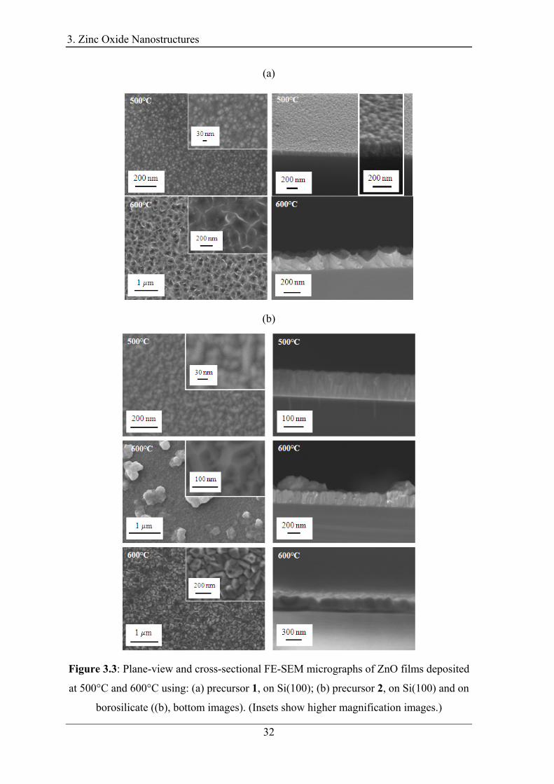
3. Zinc Oxide Nanostructures
32
(a)
(b)
Figure 3.3: Plane-view and cross-sectional FE-SEM micrographs of ZnO films deposited
at 500°C and 600°C using: (a) precursor 1, on Si(100); (b) precursor 2, on Si(100) and on
borosilicate ((b), bottom images). (Insets show higher magnification images.)

3. Zinc Oxide Nanostructures
33
(a)
µm
1.0
1.5
2.0
0.5
500 °C 20 nm
0
µm
1.0
1.5
2.0
0.5
600 °C 300 nm
0
RMS roughness = 3 nm RMS roughness = 42 nm
20 nm
0 nm
2 µm 2 µm
300 nm
0 nm
500ƒC 600ƒC600°C500°C
(b)
µm
1.0
1.5
2.0
0.5
500 °C
0
50600 °C
1.0
1.5
2.0
0.5
µm
0
100
100 nm
0 nm
2 µm 5 µm
200 nm
0 nm
500 °C 600 °C
RMS roughness = 5 nm RMS roughness = 25 nm
Figure 3.4: AFM micrographs of ZnO films deposited on Si(100) using: (a) precursor 1;
(b) precursor 2.
500°C 600°C
600°C 500°C

3. Zinc Oxide Nanostructures
34
3.3.3 Composition
RBS was employed to determine the film stoichiometry, and the presence of Zn and O in
the spectra of a ZnO film grown at 600°C is clearly seen (figure 3.5). The thickness of
the layer is in agreement with the value determined by the SEM image (figure 3.3),
taking into account the surface roughness. The recorded spectrum is described by a
simulation of a 190 nm thick layer of zinc (41 at. %), oxygen (45 at. %) deposited on a
silicon substrate. In comparison to the simulated data, the broadening of the Si edge and
of the low-energy Zn edge can be attributed to the surface roughness of the layer (figure
3.3). The spectrum indicates the presence of carbon in the range of 5 weight %, proximate
to its detection limit, thus indicating that the precursor is able to provide the ZnO material
in the right stoichiometry.
0
500
1000
1500
2000
2500
3000
3500
4000
4500
5000
100 200 300 400 500 600
co
un
ts
channel
recorded spectrum
simulated spectrum
C
Si
Zn
O
yiel
d(c
ount
s/ µ
C)
0
150
100
50
200
250
300 1800energy (keV)
C
O
Si
Zn
recorded spectrum
simulated spectrum
Figure 3.5: Representative RBS spectrum of ZnO grown at 600°C by using compound 1.
The surface and in-depth chemical composition of the ZnO films were investigated by
XPS, yielding very similar results for films obtained from both precursors. Representative
XPS spectra of Zn and O peaks are reported in figure 3.6, both before and after Ar+
erosion. Irrespective of the process conditions and the used precursor, the Zn2p3/2 and
Zn3p3/2 spin-orbit components were centered at binding energies (BE) = 1021.8 and 88.9
eV, as expected for ZnO. [Barreca-2007-C, Barreca-2003-B, Moulder-1992, Nist] The
fingerprint for the presence of the sole zinc(II) oxide was provided by the evaluation of
the Auger parameter [Zn = BE(Zn2p3/2) + KE(ZnLMM), where KE = kintetic energy],
which was 2010.2 eV for all films grown from precursors 1 and 2. This value is in

3. Zinc Oxide Nanostructures
35
excellent agreement with literature data for ZnO. [Armelao-2006, Armelao-2008,
Barreca-2007-C, Briggs-1990, Moulder-1992]
100 95 90 85 80BE (eV)
a) b)
Zn3p
536 532 528BE (eV)
a) b)
O1s
100 95 90 85BE (eV)
a) b)
Zn3p
Int
ensi
ty (
a.u.
)
1025 1020BE (eV)
a) b)
Zn2p3/2
536 532 528BE (eV)
a) b)I
II
O1s
Inte
nsit
y (a
.u.)
1025 1020BE (eV)
a) b)
Zn2p3/2
j=1/2
J=3/2
J=1/2
J=3/2
Inte
nsit
y (a
.u.)
Inte
nsit
y (a
.u.)
BE (eV)
BE (eV)BE (eV)BE (eV)
BE (eV)BE (eV)
Zn2p3/2Zn3p O1s
Zn3p O1sZn2p3/2
Figure 3.6: Representative XPS zinc and oxygen signals for ZnO samples grown at
600°C from precursor 1 (top) and 2 (bottom): (a) surface; (b) after 8 min Ar+ erosion. For
the second specimen, the fitting components for the surface O1s peak are also displayed
along with the raw spectrum.
The surface O1s signal could be decomposed by means of two contributions (figure 3.6).
The most intense one (I, BE = 530.4 eV) was attributed to Zn-O-Zn bondings of the oxide
phase, whereas the minor one (II), centered at BE = 532.0 eV, could be mainly assigned
to surface -OH groups, whose presence is frequently observed on a ZnO surface.
[Armelao-2006, Armelao-2008, Barreca-2007-C, Bekermann-2010-B, Scalisi-2008]
Contributions to this component from carbonate species arising from air exposure were

3. Zinc Oxide Nanostructures
36
also likely to be present, as confirmed from the surface C1s line shape (not shown), that
displayed a minor component located at BE = 288.4 eV. [Moulder-1992, Nist] As a result,
typical surface O/Zn atomic ratios were higher than the expected value for ZnO (1.8 –
2.0). Nevertheless, the O1s II component disappeared to noise level after Ar+ erosion,
thus indicating that the above species essentially arose from contact with the outer
atmosphere. Correspondingly, the O/Zn ratio nearly approached the stoichiometric value
(~ 1.1).
100
80
60
40
20
0
Ato
mic
%
200150100500Sputtering time (min)
Zn O C Si
2011.0
2010.0
2009.0
(e
V)
200150100500Sputtering time (min)
experimental theoretical
Figure 3.7: XPS depth profile of a ZnO sample grown from precursor 2 at 600°C. In the
inset, the dependence of the Auger parameter on the sputtering time is shown. [Moulder-
1992]
Further insight into the in-depth film composition was gained by XPS profiling (figure
3.7). It is noteworthy that the carbon signal completely disappeared after only 3 min Ar+
sputtering, thus confirming that it arose from the atmospheric contamination of the
sample surface. This feature, along with the absence of any nitrogen signal from the
precursor ligands, indicates that the precursor decomposition was a clean process, leading
to impurity-free ZnO under the adopted conditions. In addition, zinc and oxygen signals
had a ratio close to the theoretical value throughout the bulk of the film, apart from an
oxygen excess at the interface with the substrate that could be attributed to the presence
of a native silica layer on Si(100). The Auger Zn parameter dependence on depth (figure

3. Zinc Oxide Nanostructures
37
3.7, inset) confirmed the uniform formation of zinc(II) oxide throughout the sample
thickness.
3.3.4 Optical Properties
Selected UV-Vis transmission spectra recorded for samples obtained from precursor 1 on
borosilicate glass are depicted in figure 3.8. All the samples exhibited a transmittance >
60% in the visible region, and a sharp UV absorption edge located at = 370 nm, related
to the characteristic ZnO band-to-band transitions. [Armelao-2006, Malandrino-2005]
The optical band gap Eg was evaluated from the Tauc plot (h)2 vs. h (figure 3.8,
inset), where is the absorption coefficient computed from the recorded spectra by
extrapolating the trend to zero absorption. [Periasamy-2002, Barreca-2003-B] For all the
analyzed ZnO films, the obtained Eg values were close to 3.3 eV, which is in agreement
with the literature for stoichiometric ZnO. [Armelao-2006]
Abs
orba
nce
(a.u
.)
800700600500400(nm)
500°C
600°C
80x109
60
40
20
(h
)2 (eV
/cm
)2
3.43.23.02.82.6h(eV)
EG = 3.3 eV
Figure 3.8: Representative optical spectra of ZnO thin films grown on borosilicate
substrates from precursor 1. Inset: Tauc plot of (h)2 vs. h for the specimen grown at
600°C.

3. Zinc Oxide Nanostructures
38
The optical properties of the as-deposited ZnO layers were also investigated by means of
PL measurements. Figure 3.9 displays the PL spectra of ZnO films on Si(100) obtained
from precursor 2 at 500 and 600°C. At room temperature, the former sample showed a
high quality excitonic peak of ZnO at 3.30 eV (376 nm) [ Bekermann-2010-B, Li-2007-A]
with a full width at half maximum (FWHM) of 18 nm. The room temperature PL
spectrum of the deposit obtained from precursor 2 at 600°C shows an even narrower
FWHM of 13 nm. The small FWHM values of the excitonic peaks measured at room
temperature demonstrated the high crystalline quality of the ZnO samples. Irrespective of
the laser intensity, all samples gave maximum response at 3.30 eV at room temperature
(figure 3.9 (b) and (d)). At 77 K, the maximum was shifted to 3.37 eV ((a) and (c)), in
agreement with previous reports. [Li-2007-A, Teke-2004] This so-called Varshni shift
arises from shifts in the relative position of EC (conduction band) and EV (valence band)
(i) due to the temperature dependence of the thermal expansion of the lattice, and (ii)
because of temperature-dependent electron/lattice interactions. [Varshni-1967] At
variance with most literature data, no PL signals due to deep level emission defects (VO,
VZn, Zni, and Oi) in the region 420 - 540nm could be detected. [Bekermann-2010-B,
Jeong-2004, Kuang-2005, Liu-2004-A, Mikrajuddin-2001, Park-2006, Wang-2009-A]
350 400 450 500 550
0,0
0,2
0,4
0,6
0,8
1,0 (a) (b) (c) (d)
Inte
nsit
y (a
.u.)
Wavelength (nm)
1.0
0.8
0.6
0.4
0.2
0.0
(nm)
Figure 3.9: Normalized PL spectra of ZnO films on Si(100) grown from precursor 2 at
500°C, (a) 77 K and (b) room temperature; and at 600°C, (c) 77 K and (d) room
temperature (excitation power = 20 W / cm2).

3. Zinc Oxide Nanostructures
39
3.4 PECVD of ZnO Nanostructures on Si(100) and Polycrystalline Al2O3
3.4.1 Deposition Procedure
PECVD of ZnO nanorods from [Zn{[(CH2)xOCH3]NC(CH3)=C(H)C(CH3)=O}2] (1: x =
2; 2: x = 3) was carried out by a RF (ν = 13.56 MHz) two-electrode custom-built
apparatus (8.3.3). Growth experiments (duration = 1 h) were performed under Ar/O2
plasmas (total Ar (O2) flow rate = 75 (20) sccm) and at a total pressure of 1.0 mbar. p-
Type Si(100) substrates were cleaned, without removing the native oxide layer, by
iterative dipping in sulfonic detergent and distilled water, distilled water, acetone, and
isopropylic alcohol. [Armelao-1998, Bekermann-2010-B]
Table 3.2: Overview of sample labeling as a function of substrate, precursor, deposition
temperature and RF-power. Pressure, deposition time and Tvap were 1 mbar, 60 min and
140°C, respectively for all depositions.
Substrate Si(100)
Precursor 1 2
RF-
power 40 W 20 W 10 W 20 W
T (°C)
100 1_100_40W(Si) 1_100_20W(Si) 2_100_20W(Si)
200 1_200_40W(Si) 1_200_20W(Si) 2_200_20W(Si)
300 1_300_40W(Si) 1_300_20W(Si) 1_300_10W(Si) 2_300_20W(Si)
400 1_400_40W(Si) 1_400_20W(Si) 2_400_20W(Si)
Substrate Al2O3
Precursor 1 2
RF-
power 20 W 20 W
T (°C)
200 1_200_20W(Al) 2_200_20W(Al)
300 1_300_20W(Al) 2_300_20W(Al)
The Zn(II) ketoiminate precursors were vaporized in an external vessel maintained at
140°C by means of an oil bath and transported into the deposition zone through an Ar

3. Zinc Oxide Nanostructures
40
flow. The gas lines connecting the precursor reservoir and the reactor chamber were
maintained at 160°C by means of heating. For all experiments, the deposition time and
interelectrode distance were set at 1 h and 6 cm, respectively. The labeling of the present
samples is reported in table 3.2.
3.4.2 Morphology and Structure
3.4.2.1 ZnO Nanorod Growth on Si(100) from 1
In the case of precursor 1, the combined influence exerted by the growth temperature and
the applied RF-power, both related to the energy supply during the deposition process,
was investigated. To this regard, figure 3.10 provides a comparative FE-SEM
morphology overview for samples synthesized from precursor 1 (see table 3.2). As can
be observed, the use of high RF-power values (40W samples, 1_100_40W(Si) –
1_400_40W(Si)) resulted in the obtainment of relatively compact system morphology. In
particular, variations of the substrate temperature from 100 to 400°C produced a thickness
increase from ≈ 60 nm to ≈ 150 nm (table 3.3). While the 1_100_40W(Si) sample
showed the presence of pseudo-globular particles typical for an isotropic growth, the
development of a columnar morphology was evidenced for specimens 1_200_40W(Si)
and 1_300_40W(Si). In particular, the 300°C sample (1_300_40W(Si)) presented the
most pronounced anisotropy, with the formation of some faceted tips on the column
surface. Conversely, at 400°C (1_400_40W), a compact ZnO film characterized by a
rather smooth surface was obtained. Even though at 20 W (samples 1_100_20W(Si) –
1_400_20W(Si)) a qualitatively similar evolution was observed as a function of the
substrate temperature, the system morphology was systematically characterized by a more
pronounced 1D growth with respect to specimens synthesized at 40 W (1_100_40W(Si) –
1_400_40W(Si)). This difference could be traced back to an enhanced energy supply to
the substrate surface at 40 W, leading to more marked coalescence phenomena between
adjacent nanoaggregates and to an increased lateral growth. [Jeong-2008, Park-2006]
Regarding samples synthesized at 20 W, the most interesting results were obtained at
intermediate temperatures, that is, for 1_200_20W(Si) (200°C) and 1_300_20W(Si) (300
°C). In fact, under these conditions ordered arrays of NRs aligned perpendicularly to the
substrate surface were grown, with an aspect ratio (length/diameter) increasing from 9.5
at 200°C to 12.4 at 300°C. In the case of sample 1_300_20W(Si), having the more

3. Zinc Oxide Nanostructures
41
pronounced 1D morphology, the density of these nanostructures per unit area, estimated
by plane-view images, was ≈ 950 nanorods/μm2.
100 nm
100 nm
100 C 200 C 300 C 400 C
10 W
100 nm 100 nm 100 nm 100 nm
100 nm 200 nm
200 nm
100 nm
200 nm
20 W
40 W
Figure 3.10: Cross-section FE-SEM micrographs of Si(100)-supported ZnO nanodeposits
synthesized from precursor 1 as a function of the adopted RF-power and growth
temperature (see tables 3.2 and 3.3). For sample 1_300_20W(Si), representative plane-
view and high magnification cross-section images are also reported.
An increase of the growth temperature up to 400°C (sample 1_400_20W(Si)) resulted in
the formation of a relatively compact cross-section texture, although the surface appeared
rougher than in the case of 1_400_40W(Si). This phenomenon suggested that, at 400°C, a
reduction of the applied RF-power produced a progressive transformation from a compact
film to a columnar one, [Park-2006] accompanied by an enhancement of the overall
system thickness (i.e. of the GR, table 3.3). A similar effect indicated that the use of more
drastic RF-power conditions favored etching phenomena over the competitive deposition
ones, [Li-2003] whereas the use of a lower RF-power (20 W) had a beneficial influence
on the GR and also induced an improvement of the anisotropic 1D morphology. In order
to further ascertain the latter effect, PECVD of ZnO from precursor 1 was also
undertaken at 300°C and 10 W (1_300_10W(Si)). Under these conditions columnar
structures were still obtained, but the deposit thickness (130 nm) and aspect ratio (4.9)
were appreciably lower than for the corresponding sample (1_300_20W(Si)) obtained at
20 W. The above results, in line with previous literature works, [Falyouni-2009, Jeong-
100 °C 200 °C 300 °C 400 °C

3. Zinc Oxide Nanostructures
42
2007, Kim-2009, Li-2003] highlight the need for intermediate growth temperatures and
RF-power values to obtain anisotropic ZnO NR arrays.
Table 3.3: Film thicknesses (t) for Si(100) supported samples obtained from 1 (see table
3.2).
Sample t (nm) Sample t (nm) Sample t (nm)
1_100_40W(Si) 65 1_100_20W(Si) 70
1_200_40W(Si) 90 1_200_20W(Si) 250
1_300_40W(Si) 105 1_300_20W(Si) 405 1_300_10W(Si) 130
1_400_40W(Si) 150 1_400_20W(Si) 330
GIXRD analyses on specimens 1_100_40W(Si) – 1_400_40W(Si) and 1_100_20W(Si) –
1_400_20W(Si) (figure 3.11) evidenced the sole reflections expected for the hexagonal
ZnO wurtzite structure (zincite; [JCPDS-A]). Nevertheless, both the relative peak
amplitudes and the total diffracted intensity were significantly influenced by the synthesis
conditions. At 100°C, the recorded patterns were characterized by four well-evident
reflections at 2 = 31.8, 34.4, 36.3, and 47.5°, attributed respectively to ZnO (100), (002),
(101), and (102) reflections. [JCPDS-A] The relative intensities of the observed peaks
suggested the absence of marked preferential orientation effects. This result, in line with
the observed globular morphology of both 1_100_40W(Si) and 1_100_20W(Si) samples
(compare figure 3.10), confirmed the occurrence of an isotropic crystallite growth. [Fu-
2007-B, Ali-2009] In a different way, for ZnO nanodeposits synthesized in the 200 -
400°C range, a strong c-axis preferential orientation was always observed, as indicated by
the remarkable intensity of the (002) peak with respect to the other reflections (figure
3.11). The total diffracted intensity for samples synthesized at the same temperature was
always higher at 20 W, in agreement with the increased deposit thickness applying 20 W
of RF-power (see also figure 3.16). It is worthwhile observing that for specimen
1_300_20W(Si), characterized by the most anisotropic 1D architecture, the GIXRD
pattern was dominated by the (002) reflection. This result, highlighting the occurrence of
a direct relationship between the sample structure and morphology, indicated that the
observed ZnO NRs were characterized by a <001> growth direction perpendicular to the
substrate surface. [Jeong-2008, Lee-2005, Li-1999, Liu-2004-A, Umar-2006, Wang-2005-
A, Wu-2009, Zhang-2006-A]

3. Zinc Oxide Nanostructures
43
2 °
Inte
nsit
y (a
.u.)
504540353025
1_400_20W(Si)
1_400_40W(Si)
Inte
nsit
y (a
.u.)
504540353025
1_300_20W(Si)
1_300_40W(Si)
2 °
Inte
nsit
y (a
.u.)
504540353025
1_200_40W(Si)
1_200_20W(Si)
2 °
Inte
nsit
y (a
.u.)
504540353025
1_100_40W(Si)
1_100_20W(Si)
2 °
Figure 3.11: GIXRD spectra for samples 1_100_40W(Si) – 1_400_40W(Si) and
1_100_20W(Si) – 1_400_20W(Si) deposited on Si(100) from precursor 1.
In order to attain a deeper insight into the structure and morphology of the synthesized
ZnO nanosystems, selected specimens were subjected to TEM and high-resolution TEM
(HR-TEM) analyses. Figure 3.12 (a) and (b) display the low magnification cross-section
structure of samples 1_200_20W(Si) and 1_300_20W(Si). The observed topological
features were in excellent agreement with results provided by FE-SEM investigation
(compare figure 3.10) and confirmed the formation of uniform NR arrays oriented
perpendicularly to the substrate surface, with aspect ratio values directly dependent on the
synthesis conditions. As already discussed in paragraph 3.2.2, the obtainment of ZnO
1D growth under optimized synthetic conditions is usually related to the non-
centrosymmetric hexagonal wurtzite structure, and, in particular, to the divergence of
surface energies, resulting in diversified GRs as a function of crystallographic directions.
[Barreca-2007-B, Li-1999, Wang-2008-A, Wu-2002, Wu-2009] Nevertheless, the sole
occurrence of an anisotropic growth regime is not sufficient to ensure the alignment of the

3. Zinc Oxide Nanostructures
44
resulting NRs perpendicular to the substrate surface. To this regard, an epitaxial
relationship with the Si(100) support cannot explain the obtained results, since a native
SiO2 layer ≈ 2 nm thick was always present at the ZnO/substrate interface (see figure
3.12 (c)). [Lee-2005, Liu-2004-A Scalisi-2008,] In the present case, a reasonable
justification for the highly oriented growth of ZnO NRs relies on the intrinsic polarization
along the c-axis of the wurtzite structure, favoring the rod alignment in the direction of
the applied electric field, that is, normal to the substrate surface. [Li-1999, Liu-2009-B,
Liu-2004-A, Wang-2008-A]
Figure 3.12: Cross-section low magnification TEM images of samples (a)
1_200_20W(Si) and (b) 1_300_20W(Si). (c) Representative HR-TEM image of the
ZnO/substrate interface for specimen 1_200_20W(Si).
HR-TEM analyses confirmed that ZnO NRs always grew along the <001> direction, that
is, with the c-axis mainly perpendicular to the substrate surface (see figure 3.13).
Although this effect was common to all 1D ZnO nanodeposits, other structural features
were found to be directly dependent on the specific synthesis conditions. In this regard,
figure 3.13 shows some important differences between samples 1_200_20W(Si) (200°C)
and 1_300_20W(Si) (300°C) obtained at 20 W RF-power. As can be observed, stacking
faults (SF) were the main type of defects in both cases, but their density was appreciably
higher for 1_200_20W(Si). This phenomenon suggested that an increase of only 100°C in
the growth temperature resulted in a more efficient ZnO crystallization. Such an effect,
also confirmed for samples synthesized from precursor 2 (figure 3.15), was responsible
for the different optical properties of the corresponding ZnO NR arrays (see PL results,
paragraph 3.4.4). The most common type of SF for all samples was found to be the one
shown in figure 3.13 (b). As the stacking sequence of 2H-ZnO structure can be
represented as ABABAB along the c direction, this SF can be described as ABABACAC
(I1 type). [Stampfl-1998] The displacement vector R can be determined as 1/3 [100]. Only

3. Zinc Oxide Nanostructures
45
in sample 1_200_20W(Si), besides the above quoted I1 SF, some ZnO NRs exhibit a
different type of SF sequence - ABABCBACA (figure 3.13 (a)). This alternative stacking
structure can be described either as a 4H-type structure inserted in 2H-ZnO
(AB/ABCBA/CA), or as an I1 type SF with an additional two-layer insertion, that is,
ABAB/CB/ACAC. In this case, the displacement vector R is 2/3 [100].
Figure 3.13: Cross-section HR-TEM images of single ZnO NRs in samples (a)
1_200_20W(Si) and (b) 1_300_20W(Si), obtained from precursor 1. White arrows mark
SF along the <001> growth direction. The areas highlighted by white rectangles are
enlarged at the bottom of the figure to show different SF types in the two samples. In (b),
two adjacent NRs grown with a similar <001> orientation are imaged.
3.4.2.2 ZnO Nanorod Growth on Si(100) from 2
On the basis of the results presented so far, the attention was devoted to the use of
compound 2 as the PECVD precursor and to a comparative analysis of the resulting ZnO
nanosystem properties. In this case, samples were synthesized adopting an applied RF-
power of 20W (table 3.2), corresponding to the best conditions for the obtainment of ZnO
NR arrays in the case of compound 1. In particular, the influence of the growth
temperature on the system morphological evolution was investigated for samples
2_100_20W(Si) - 2_400_20W(Si) (figure 3.14). Once again, ZnO NRs with the highest

3. Zinc Oxide Nanostructures
46
aspect ratio (13.0) and the mostly pronounced anisotropic 1D morphology were obtained
at 300°C. Nevertheless, two important differences are worth being highlighted with
respect to specimens 1_100_20W(Si) - 1_400_20W(Si), obtained from precursor 1 at the
same RF-power (20W) and growth temperatures. First, in this case, even the sample
obtained at 400°C (2_400_20W(Si)) presented a well-evident 1D morphology, at
variance with the homologous 1_400_20W(Si) grown at the same temperature. In
addition, under the same processing conditions, the growth rate from precursor 2 was
appreciably higher than in the case of compound 1 (table 3.4, figure 3.16), in agreement
with results from paragraph 3.2 (figure 3.1).
200 nm
100 C 200 C 300 C 400 C
100 nm
100 nm 200 nm200 nm
Figure 3.14: Representative cross-section FE-SEM micrographs of Si(100)-supported
ZnO specimens synthesized from precursor 2 as a function of the adopted growth
temperature (see tables 3.2 and 3.4). For sample 2_300_20W(Si), a plane-view image is
presented.
Also in the case of precursor 2, ZnO nanosystems possessing the most pronounced 1D
morphology were investigated by TEM. Once again, the obtained results, that agreed to a
good extent with FE-SEM ones (figure 3.15), revealed an appreciable density of SFs and
a NR faceting directly dependent on the synthesis conditions. Figure 3.15 shows HR-
TEM images of ZnO NRs obtained from precursor 2 (2_200_20W(Si) and
2_300_20W(Si)). Similar to the corresponding samples obtained from precursor 1
(compare figure 3.13), even in this case the SF density was appreciably higher at 200°C
than at 300°C. As evidenced by HR-TEM imaging (figure 3.15 (a)), SFs perpendicular to
the growth direction were clearly related to the nanorod faceting, the main exposed planes
100 °C 200 °C 300 °C 400 °C

3. Zinc Oxide Nanostructures
47
being {101} and {100}. The common <001> growth direction led to a perfect
heteroepitaxial intergrowth of adjacent nanorods (figure 3.15 (b)), with an atomically
sharp boundary free from amorphous or intermediate layers.
Table 3.4: Film thicknesses for Si(100) supported samples obtained from 2 (see table
3.2).
Sample thickness (nm)
2_100_20W(Si) 110
2_200_20W(Si) 355
2_300_20W(Si) 505
2_400_20W(Si) 410
Figure 3.15: Cross-section HR-TEM images of single ZnO NRs in samples (a)
2_200_20W(Si) and (b) 2_300_20W(Si), obtained from precursor 2. In (a), white arrows
mark SFs along the <001> growth direction. Exposed surface planes are also labeled.
Figure (b) shows the intergrowth of two adjacent NRs (A and B). The presence of a SF in
NR B, that stops at the boundary with A (marked by a black arrow), is also highlighted by
the white rectangle and enlarged at the bottom of the figure. The fast Fourier transform
(FT) along the [010] zone is reported in the inset.

3. Zinc Oxide Nanostructures
48
3.4.2.3 Summary: ZnO Nanorod Growth on Si(100) from 1 and 2
On the basis of the above results, a general growth mechanism can be proposed as a
function of the adopted synthetic parameters. In this regard, figure 3.16 summarizes the
dependence of the growth rate on the deposition temperature for samples synthesized
from compounds 1 and 2. Interestingly, irrespective of the used precursor, four growth
regimes, corresponding to different morphological features, can be identified in the graph.
In particular, specimens grown at 100°C are characterized by an isotropic growth, that is,
by the formation of pseudo-globular particles (compare figures 3.10 and 3.14).
Reasonably, at the lowest deposition temperature (100°C), the limited thermal energy
supply was the main factor preventing the 1D growth, irrespective of the adopted RF-
power (20 or 40 W). Upon increasing the deposition temperature to 200 - 300°C, two
growth regimes can be observed, namely, a columnar (“quasi-1D”) and a 1D one,
corresponding to the formation of ZnO NRs, occurring at higher growth rates. Similar
results have also been recently reported in the PECVD of TiO2 from Ti(IV) isopropoxide.
[Borras-2009]
8
6
4
2
0
grow
th r
ate
(nm
/min
)
400350300250200150100deposition temperature (°C)
2_300_20W(Si)
isotropic growth
1D growth
columnar growth
compact films
columnarfilms
2_200_20W(Si)
1_300_20W(Si)
1_200_20W(Si)
Precursor 2; 20WPrecursor 1; 20WPrecursor 1; 40WPrecursor 1; 10W
Figure 3.16: Synoptic diagram showing the dependence of the ZnO morphology on
PECVD growth parameters. Red and blue markers correspond to ZnO samples
synthesized from precursors 1 and 2, respectively. (See table 3.2, figures 3.10 and 3.14.)

3. Zinc Oxide Nanostructures
49
Furthermore, the morphology of the NR arrays with the most pronounced 1D growth
(2_200_20W(Si), 1_300_20W(Si) and 2_300_20W(Si)) was investigated by AFM
imaging. The RMS roughness, an important parameter in the functionalization of
nanostructures (see paragraph 3.4.5), was found to depend on the NR length and density,
so that 2_300_20W(Si), that has the longest and most sparsely grown NRs, showed the
highest RMS roughness value of 5.8 (figure 3.17).
Sample
NRs length (nm)
NRs density
(NRs/m2)
RMS roughness
(nm)
2_200_20W(Si) 356 710 3.2
1_300_20W(Si) 405 950 2.6
2_300_20W(Si) 504 620 5.8
low RMSroughness
high RMSroughness
high NRdensity
low NRdensity
Figure 3.17: (a) RMS roughness values of selected NR arrays; (b) AFM of
2_300_20W(Si); (c) Sketch of the morphology of ZnO 1D NR arrays grown at different
PECVD parameters (see also figure 3.16).
As a whole, the present findings provide a useful guideline for the control of the ZnO
system morphogenesis from a phenomenological point of view. In the absence of
epitaxial relationships with the substrate, as in the present case, a possible explanation for
the obtainment of highly oriented NRs is as follows. At the beginning of the deposition
process, the formation of small ZnO seeds takes place. At intermediate temperatures (200
or 300°C) and in the presence of plasma activation, such crystallites mainly grow with
{001} planes parallel to the substrate surface since this orientation, characterized by a
spontaneous polarization, is favored by the applied electric field. As the growth process
proceeds, these ZnO nanoparticles act as self-catalysts for the formation of ZnO
anisotropic systems [Liu-2004-A, Wu-2009, Wang-2008-A] and preferentially grow along
the <001> direction when a high mass supply to the substrate surface is provided, giving
rise to the observed NR arrays. [Park-2006, Wu-2009, Wu-2002] An increase of the
(c)
0.20.4
0.60.8
m
0.20.4
0.60.8
1030
nm(a) (b)

3. Zinc Oxide Nanostructures
50
deposition temperature up to 400°C led to the formation of ZnO films maintaining a
strong <001> preferential orientation but showing a progressive evolution from compact
deposits to columnar ones upon increasing the GR (see figure 3.17). Although higher
GRs still favored the formation of more anisotropic nanostructures, the increased thermal
energy supply at 400°C resulted in an enhanced lateral growth, explaining thus the
formation of relatively compact films rather than 1D (or “quasi-1D”) systems.
3.4.2.4 ZnO Nanorod Growth on Al2O3 from 1 and 2
Encouraged by the obtainment of high quality ZnO NRs on Si(100) at relatively low
temperatures, and in order to integrate the rough NR arrays into gas sensing devices, the
above discussed PECVD procedure using precursors 1 and 2 was applied for the growth
of ZnO on polycrystalline Al2O3 at 200 - 300°C, resulting in urchin-like 1D ZnO NR
arrays with strong c-axis orientation, as shown below.
1 m
200 nm
1 m
200 nm 1_300_20W(Al) 2_300_20W(Al)
Figure 3.18: Plane-view FE-SEM micrographs of samples 1_300_20W(Al) and
2_300_20W(Al) (see table 3.2).
The morphology of the obtained ZnO systems was analyzed by FE-SEM, and it was
found to be directly dependent on the adopted synthesis conditions. For all samples,
plane-view micrographs (figure 3.18 and 3.19) evidenced the presence of globular
particles typical of the Al2O3 substrate, whose dimensions ranged from 400 nm to more
than 1 µm. Higher magnification images (see insets in figure 33.18 and 3.19) clearly
displayed smaller ZnO nanostructures uniformly decorating the substrate surface. ZnO
specimens 1_200_20W(Al) and 2_200_20W(Al), grown at 200°C, presented a relatively
compact agglomeration of globular ZnO particles (figure 3.19 (b)), while a rise of the

3. Zinc Oxide Nanostructures
51
temperature (T = 300°C), led to the formation of uniform “3D/1D” urchin-like aggregates
extending throughout the substrate surface (figure 3.18 and 3.19). m m m
(a)
1 µm
(b)
1 µm
0 1 2 3 4 5 6 7 8 9 10
0
1
2 3
4
5
6
7
8
9
10
0 1 2 3 4 5 6 7 8 9 10
0
1
2 3
4
5
6
7
8
9
10
m mmm m
0
0.5
1.0
1.5
2.0
2.5
3.0
3.5
0
0.5
1.
0 1
.5
2.0
2.5
3.
0 3
.52_200_20W(Al) 2_300_20W(Al)
(a)
200 nm
100 nm (a)
200 nm
100 nm
(b)
Al2O3 substrate ZnO nucleation urchin-like growth
(c)
200 nm 200 nm
100 nm
100 nm
(c)
Al2O3 substrate ZnO nucleation urchin-like growth
2_200_20W(Al) 2_300_20W(Al)
(b)
Figure 3.19: 10×10 μm2 AFM (a) and plane-view FE-SEM (b) micrographs for
2_200_20W(Al) (78 nm) and 2_300_20W(Al) (116 nm) are shown (see table 3.2). (The
film thicknesses are derived from SIMS, see figure 3.23.) In the insets, higher
magnification images are shown. A schematic view of the formation process of urchin-
like ZnO NR arrays is displayed in (c).

3. Zinc Oxide Nanostructures
52
ZnO deposits 1_300_20W(Al) and 2_300_20W(Al) were characterized by a
homogeneous array of 1D like structures (average diameter = 30 ± 5 nm) grown on the
surface of individual Al2O3 islands, whose surface density was depended on the adopted
synthesis conditions. Sample 1_300_20W(Al) (figure 3.18 (b)) showed uniform ZnO
arrays with 1800 nano-columns/µm2, fabricated at 300°C and by use of precursor 1. By
use of precursor 2 at the same temperature (2_300_20W(Al)), longer 1D nanostructures
with 1450 rods/µm2 were obtained.
The system morphology was further analyzed by AFM (figure 3.19 (a)). The
micrographs were dominated by the globular Al2O3 particles with a mean diameter of 600
nm. In line with FE-SEM results, higher magnification images showed that ZnO
nanograins (see insets of AFM figures) uniformly covered the underlying substrate. All
samples displayed a highly rough surface, with a RMS roughness close to 70 nm. Hence,
such nanoarchitectures are reasonably characterized by a high surface area, a key factor in
view of gas-sensing applications.
55045403530
2(degrees)
(10
0)
(00
2)
(10
1)
(102
)° °°
2 (degrees)
1
2
(a)
55045403530
2(degrees)
(10
0)
(00
2)
(10
1)
(102
)° °°
2 (degrees)
1
2
(a)
2 (°)
30 35 40 45 50
2_200_20W(Al)
2_300_20W(Al)
Figure 3.20: GIXRD patterns of 2_200_20W(Al) and 2_300_20W(Al) (see table 3.2 and
figure 3.19). Reflections of the wurtzite phase are directly indexed, whereas diffraction
peaks of the Al2O3 substrate are marked by circles.
XRD analyses (figure 3.20) showed Bragg reflections of the hexagonal ZnO wurtzite
phase characterized by a strong intensity and narrow width, indicating the formation of
high crystalline ZnO. As frequently observed for 1D ZnO nanosystems, [Bekermann-
2010-B, Hsueh-2007-B, Zeng-2009-A] a common feature to the synthesized specimens
2 (°)

3. Zinc Oxide Nanostructures
53
was the predominance of the (002) ZnO signal, ascribed to the concurrence of a
preferential c-axis orientation and an anisotropic crystallite growth, as indeed confirmed
by FE-SEM investigation.
Basing on the present data, a growth model for the observed urchin-like structures is
proposed in figure 3.19 (c). At the beginning of the deposition process, the initial
formation of small ZnO seeds takes place. Subsequently, in the presence of plasma
activation, such nanoparticles act as a self-catalyst for the development of NRs along the
<001> direction, as indicated by XRD measurements. The typical globular morphology of
the alumina substrates, is responsible for the formation of the observed urchin-like arrays
instead of parallel aligned 1D rods. [Barreca-2010-A]
3.4.3 Composition
The chemical composition of silicon and alumina supported ZnO samples was
investigated by the combined use of EDXS, XPS and SIMS. Since all ZnO specimens
revealed identical compositional information, irrespective of the substrate and processing
conditions, the results are discussed below using selected silicon or alumina based
samples as representative examples.
0 1 2 3 4 5 6 7 8 9 10 11Energy (keV)
Inte
nsity
(a.u
.)
Al
O
Zn
(c)
Zn
0 1 2 3 4 5 6 7 8 9 10 11
Energy (eV)
Inte
nsit
y(a
.u.)
Zn
Zn
Al
O
Figure 3.21: Representative EDX spectrum (here for 1_300_20W(Al), see table 3.2).
The inset shows typical EDXS profiles for O K1 (red) and Zn K1 (blue) X-ray signals
along the cross section of 2_300_20W(Si) (see table 3.2 and figure 3.14).

3. Zinc Oxide Nanostructures
54
Preliminary investigation was performed by EDXS analysis. Irrespective of the
preparation conditions, EDX spectra (figure 3.21) were characterized by the sole lines of
oxygen (O K at 0.52 keV) and zinc (L and K peaks located at 1.01 and 8.63 keV),
along with the substrate signal (Al K at 1.49 keV). No carbon that might arise from the
incorporation of undecomposed precursor residuals was detected, suggesting thus a clean
decomposition of the used Zn sources under the present PECVD conditions, as further
confirmed by the data below. From EDXS cross-section line scans (figure 3.21 inset) it
can be seen that a slight oxygen excess is present on the sample outermost layers, that
could be mainly related to the presence of -OH groups (see XPS below) arising from
atmospheric exposure (figure 3.21).
1024 1016BE (eV)
1020
Zn2p3/2
536 532 528BE (eV)
O1s
Inte
nsity
(a.
u.)
1000 800 600 400 200 0BE (eV)
Zn2p 1
/2
Zn2p 3
/2CKVV
OKLL
O1s
C1s
ZnLMM
Zn3s Z
n3p
Zn3d
1024 1016BE (eV)
1020
Zn2p3/2
536 532 528BE (eV)
O1s
Inte
nsity
(a.
u.)
1000 800 600 400 200 0BE (eV)
Zn2p 1
/2
Zn2p 3
/2CKVV
OKLL
O1s
C1s
ZnLMM
Zn3s Z
n3p
Zn3d
O1sO
1s
C1s
OK
LL
CK
VV
ZnLMM
Zn3
s Zn3
p
Zn3
d
Zn2
p 3/2
Zn2
p 1/2
Zn2p3/2
Inte
nsit
y (a
.u.)
BE (eV)1000 800 600 400 200 0
BE (eV)
BE (eV)
Figure 3.22: Representative surface XPS survey spectrum of ZnO NRs on Si(100) or
Al2O3 (see table 3.2), obtained from 1_200_20W(Al) (figure 3.18). Surface
photoelectron peaks for Zn2p and O1s photopeaks are displayed as insets, along with the
two O1s components resulting from spectral deconvolution.
To attain a deeper insight into the chemical composition, all the obtained ZnO specimens
were analyzed by XPS. To this regard, figure 3.22 reports the surface wide-scan spectrum
of a representative sample, along with the detailed Zn2p and O1s regions. (Similar XPS

3. Zinc Oxide Nanostructures
55
features for ZnO NR arrays (paragraphs 3.4.2.1 - 3.4.2.4) have been obtained, see
[Barreca-2010-C, Bekermann-2010-A, Bekermann-2010-B].) The survey displayed the
expected zinc and oxygen signals, along with the C1s and CKVV ones. The complete
disappearance of the carbon photopeaks after Ar+ sputtering, as in the case of ZnO by
CVD (paragraph 3.3.3), confirmed that its presence was limited to the outermost sample
layers and that it arose from atmospheric contamination, in agreement with EDXS results.
As regards the zinc signals, the Zn2p3/2 peak was centred at BE = 1021.2 eV ((FWHM) =
2.1 eV). This value, along with the calculation of the Auger parameter (2010.0 eV),
confirmed the formation of ZnO free from other zinc-containing phases. [Barreca-2007-
B, Briggs-1990, Qurashi-2009] The O1s peak presented a broad spectral profile that
could be fitted by two contributions (see inset of figure 3.22). While the main component
at 530.1 eV (FWHM = 1.7 eV; 65 %) was ascribed to lattice oxygen in the ZnO wurtzite
structure, the second one (BE = 531.6 eV; FWHM = 2.0 eV; 35 %) was mainly related to
hydroxyl groups arising from interaction with atmospheric H2O. [Barreca-2007-A,
Barreca-2007-C, Liangyuan-2010, Li-2007-B] The presence of such species, commonly
revealed on metal oxides, was reasonably enhanced in the present case due to the high
surface area of the obtained ZnO nanosystems, and accounted for the O/Zn ratio ( 1.3)
higher than the stoichiometric value. Such a phenomenon, was reasonably enhanced in
the present case due to the high surface-to-volume ratio of the obtained ZnO NR arrays
(see figures 3.10, 3.14, 3.18 and 3.19).
0 100 200 300 400 500100
101
102
103
104
105
106
SIM
S Y
ield
(C
ount
s/s)
Depth (nm)
O
Zn
(c)
0 100 200 300 400 500100
101
102
103
104
105
106
SIM
S Y
ield
(C
ount
s/s)
Depth (nm)
O
Zn
(c)
0 100 200 300 400 500100
101
102
103
104
105
106
100
101
102
103
104
105
106
SIM
S Y
ield
(C
ount
s/s)
Depth (nm)
O
Zn
(c)
O
Zn
Depth (nm)
106
105
104
103
102
101
100
0 100 200 300 400 500
SIM
S yi
eld
(cou
nts/
s)
0 50 100 150 200 250 300
SIM
S Y
ield
(C
ount
s/s)
Depth (nm)
O
Zn
100
101
102
103
104
105
106
(b)
0 50 100 150 200 250 300
SIM
S Y
ield
(C
ount
s/s)
Depth (nm)
O
Zn
100
101
102
103
104
105
106
(b)
0 50 100 150 200 250 300
SIM
S Y
ield
(C
ount
s/s)
Depth (nm)
O
Zn
100
101
102
103
104
105
106
100
101
102
103
104
105
106
(b)
O
Zn
0 50 100 150 200 250 300
106
105
104
103
102
101
100
Depth (nm)
SIM
S yi
eld
(cou
nts/
s)2_200_20W(Al) 2_300_20W(Al)
Figure 3.23: SIMS depth profiles for samples 2_200_20W(Al) and 2_300_20W(Al) (see
table 3.2 and figure 3.19).
The in-depth chemical composition of the present specimens was further investigated by
SIMS analyses (figure 3.23). As a general rule, the ZnO nanodeposits presented a

3. Zinc Oxide Nanostructures
56
uniform and parallel Zn and O distribution up to the interface with the substrate,
confirming thus their common chemical origin, in agreement with EDXS and XPS data.
3.4.4 Optical Properties
To gain further information about the quality of Si(100) supported ZnO NR arrays, the
optical properties of two selected ZnO NR arrays (2_200_20W(Si) and 2_300_20W(Si)),
characterized by the most pronounced 1D morphology (see section 3.4.2.3 and figure
3.16) were investigated by PL measurements (figure 3.24).
inte
nsit
y (a
.u.)
650600550500450400350wavelength (nm)
ZnO11 ZnO122_300_20W(Si)
2_200_20W(Si)
350 400 450 500 550 600 650
(nm)
Inte
nsit
y(a
.u.)
Figure 3.24: PL spectra of sample 2_200_20W(Si) (200°C) and 2_300_20W(Si) (300°C)
(see section 3.4.2.2 and figure 3.16).
In the case of sample 2_200_20W(Si), the PL spectrum presented a strong UV peak
centered at 384 nm, displaying an appreciable tailing toward higher wavelengths. This
signal was ascribed to the near band-edge emission of ZnO, originated from free exciton
recombination. [Kuang-2005, Liu-2004-A, Umar-2006, Wu-2009, Wang-2005-A] On the
other hand, the emission in the visible region could be traced back to the combined
contribution of various kinds of defects for NRs synthesized at 200°C, even though their
exact nature can be hardly deduced from the present spectrum. [Rowlette-2009, Scalisi-
2008] In a different way, the PL spectrum of sample 2_300_20W(Si) presented a
narrower excitonic band centered at 374 nm. The blue-shift of the UV band with respect

3. Zinc Oxide Nanostructures
57
to specimen 2_200_20W(Si) could be related to the higher surface-to-volume ratio for
2_300_20W(Si) specimen (see figure 3.14 and 3.17). [Jeong-2008] In fact, although the
average NR diameter was ≈ 40 nm in both cases, their aspect ratio was appreciably
different (9.1 for 2_200_20W(Si) and 13.0 for 2_300_20W(Si)).
Regarding 2_300_20W(Si), an additional structured emission band in the region between
420 and 540 nm was also detected and ascribed to the presence of point defects, such as
VO and Zni. [Kim-2005-B, Kuang-2005, Liu-2004-A, Park-2006, Wu-2009]
3.4.5 PSH and PCO Properties
For PSH and PCO applications, a high surface-to-volume ratio, like in the case of the
above described ZnO NRs (sections 3.4.2.1 - 3.4.2.3), is generally considered favorable,
since it enables a faster arrival of photo-generated electrons and holes to the surface,
reducing detrimental recombination phenomena. [Wan-2005, Zhang-2009-A] Therefore,
in the following, the silicon based ZnO NR arrays of highest aspect ratio and roughness,
namely 1_200_20W(Si), 1_300_20W(Si), 2_200_20W(Si) and 2_300_20W(Si) (figure
3.16 and 3.17), were investigated regarding PSH and PC. Special attention was devoted to
the interrelations between the photo-activity of the obtained 1D ZnO systems and their
morphological characteristics.
PSH properties were analyzed by monitoring the evolution of water contact angle (WCA)
as a function of the UV irradiation time (paragraph 8.6.1). The self-cleaning activity of
the synthesized NRs was investigated through a novel quantitative and highly sensitive
PCO method (8.6.2), based on the determination of the TPA oxidation product HOTPA:
[Černigoj-2010]
(reaction 3.1)
As regards PSH properties, specimen 1_200_20W(Si) presented the lowest activity
among the analyzed samples. Such an effect was ascribed both to the reduced NR length,
responsible for less efficient light absorption, [Barreca-2007-B, Zhang-2009-A] and to the
COOH
COOH
COOH
OH
COOH
h, catalyst+ other products

3. Zinc Oxide Nanostructures
58
relatively compact cross-sectional structure (figure 3.10), resulting in a lower active area.
In a different way, ZnO NR arrays thicker than 300 nm, namely 1_300_20W(Si) (figure
3.10), 2_200_20W(Si) and 2_300_20W(Si) (figure 3.14), presented remarkable PSH
performances with a very fast hydrophobic-to-superhydrophilic conversion upon UV
exposure (figure 3.25). The initial hydrophobic WCA value was close to 120° for all
samples, in agreement with previous reports. [Badre-2009, Barreca-2009-A, Fujishima-
2008, Liu-2004-B, Meng-2005] This phenomenon was mainly attributed to adventitious
carbon contamination, as evidenced by XPS (see figure 3.22).
0.20.4
0.60.8
m
0.20.4
0.60.8
1030nm
AFM
120
100
80
60
40
20
0
WC
A (
)
250200150100500irradiation time (min)
2_200_20W(Si)1_300_20W(Si)
2_300_20W(Si)
before UV after UV
Figure 3.25: PSH behaviour of Si(100) supported ZnO NRs 1_300_20W(Si),
2_200_20W(Si) and 2_300_20W(Si) (see section 3.4.2.3): WCA as a function of
irradiation time. Photographs of H2O droplets on sample 2_300_20W(Si) before (left) and
after 150 min (right) UV irradiation.
Upon UV irradiation, a fast WCA decrease was observed. The present performances were
significantly better than those of the standard Pilkington® glass, the benchmark TiO2
material, and also higher than those of ZnO nanosystems, tested under similar operating
conditions. [Barreca-2009-A, Liu-2004-B, Fujishima-2008] It is worth observing that, for
specimens 1_300_20W(Si), 2_200_20W(Si) and 2_300_20W(Si), the hydrophobic-to-
superhydrophilic conversion kinetics did not improve in the same order of the NR length
(figure 3.25, compare tables 3.3 and 3.4). In fact, the performances of the sample with
shortest NRs, 2_200_20W(Si), were intermediate between those of 1_300_20W(Si) and
2_300_20W(Si). Such results suggest that, although an increase in the NR length may
result in more efficient light harvesting, other parameters concur in determining the
Irradiation time (min)

3. Zinc Oxide Nanostructures
59
system PSH activity, such as surface chemical composition and topography. [Barreca-
2007-B, Feng-2004, Li-2008-A, Meng-2005]
It is also worthwhile observing that all nanodeposits were characterized by a high surface
-OH content, as evidenced by XPS (see figure 3.22). [Badre-2009, Barreca-2007-B] The
formation of hydroxyl species could be mainly traced back to the dissociative
chemisorption of atmospheric H2O on surface oxygen vacancies, whose content is
reasonably enhanced by plasma bombardment effects during PECVD. [Meng-2005,
Bekermann-2010-B] Upon UV irradiation, photo-generated holes can react with lattice O
species to form new VO. This phenomenon further promotes water chemisorption,
increasing the surface -OH amount and resulting in a superhydrophilic behaviour due to
an increased wettability. [Feng-2004, Zhou-2008] For ZnO NR arrays, a RMS roughness
increase could be related to a higher active surface area (see figure 3.17 (c)). [Liu-2004-
B] On this basis, it is reasonable to suppose that the overall hydroxyl group content
increased in the same order of RMS values, that is, 1_300_20W(Si) < 2_200_20W(Si) <
2_300_20W(Si), further supporting the PSH trends reported in figure 3.25 (a).
As regards the PCO behaviour, for all ZnO samples a progressive increase of the HOTPA
concentration vs. irradiation time was observed (figure 3.26 (a)). Under the present
conditions, TPA degradation and, consequently, HOTPA formation followed pseudo-
zero-order kinetics (rate constant = k1).
0
0
0
0
6050403020100irradiation time (min)
2_300_Si40
30
20
10
0
2_300_20W(Si)
1_300_20W(Si)
2_200_20W(Si)
2_300_20W(Si)10.0x10
-9
9.0
8.0
7.0
k1(m
ol l
-1m
in-1
)
6.05.04.03.0
RMS roughness (nm)
Figure 3.26: (a) PCO behaviour of specimen 2_300_20W(Si): HOTPA concentration as a
function of irradiation time. (b) Rate constant (k1) dependence on RMS roughness for
samples 1_300_20W(Si), 2_200_20W(Si) and 2_300_20W(Si) (see section 3.4.2.3 and
figure 3.17).
(a) (b)
HO
TPA
con
c. (
mg
l-1)
k 1
Irradiation time (min)

3. Zinc Oxide Nanostructures
60
Considering that HOTPA degradation should also be taken into account (rate constant =
k2), HOTPA concentration vs. time dependence could be described by equations 3.1 and
3.2: [Černigoj-2010]
d[HOTPA] / dt = ( k1 – k2 ) [HOTPA] (equation 3.1)
[HOTPA] = ( k1 / k2 ) ( 1 – exp( -k2 t ) ) (equation 3.2)
The trend in figure 3.26 (a) could be fitted by equation 3.2. Similarly to PSH behaviour,
systems with the highest RMS surface roughness also displayed improved PCO
performances. In fact, an increase of the k1 reaction rate constant proportional to RMS
roughness was detected for specimens 1_300_20W(Si), 2_200_20W(Si) and
2_300_20W(Si) (figure 3.26 (b)). The reasons explaining this trend are in line with
previous considerations on PSH data, as well as with the pictorial model reported in
figure 3.17. Specifically, on going from sample 1_300_20W(Si) to 2_200_20W(Si) and,
finally, to 2_300_20W(Si), the progressive RMS enhancement and the concomitant
increase of the active area have a promotional effect on the PCO processes involved. In
particular, the large content of surface oxygen vacancies, acting as capturing centers for
photogenerated electrons, minimizes charge-carrier recombination phenomena. As a
consequence, photo-generated holes are more readily available for the oxidation of
organic pollutants. Furthermore, oxygen vacancies also assist the generation of active
species, such as ·OH and O2·-, on the surface of ZnO NRs, providing thus a two-fold
beneficial contribution to PCO activity. [Liu-2009_A, Wan-2005, Wang-2008-C] For the
best-performing sample (2_300_20W(Si)), the analyses yielded k1 = 9.5 10-9 mol l-1 min-1,
a value five times higher than that of the Pilkington® glass. This difference is likely
dependent on several parameters, including the higher roughness and overall deposit
thickness of specimen 2_300_20W(Si). [Černigoj-2010, Liu-2004-B, Mills-2003] In
conclusion, by tailoring the morphological features of the obtained ZnO NR arrays (RMS
roughness, NR length and density), the PSH and PCO properties could be tuned as a
function of the system characteristics.

3. Zinc Oxide Nanostructures
61
3.4.6 Gas Sensing Properties
The gas sensing properties of the alumina supported “3D/1D” ZnO assemblies have been
tested for the first time in the detection of various analytes, both reducing (CH3CH2OH,
CH3COCH3, CO, H2, CH4) and oxidizing (O3, NO2) gases. (Technical details and
definitions of responses, response and recovery times can be found in paragraph 8.6.4.)
In general, the obtained urchin-like 1D ZnO NR arrays 1_200_20W(Al),
1_300_20W(Al), 2_200_20W(Al) and 2_300_20W(Al) (see 3.4.2.4) displayed an
appreciable capability to detect different gaseous species. For all analytes, gas sensing
tests revealed reproducibility of the electrical responses upon prolonged utilization cycles,
an important pre-requisite for practical application.
10-7
10-8
10-9
10-10
10-11
10-12
Cur
rent
(A
)
Time (min)
0 200 400 600 800
500
400
300
200
100
0
O3
O3 (ppm
)
Cur
rent
(A
)
10-4
10-5
10-6
10-7
500
400
300
200
100
00 40 80 120 160
Time (min)
3 3
CH
3 CO
CH
3 (ppm)
Figure 3.27: Typical dynamic response of urchin-like ZnO NR arrays grown on Al2O3
from compound 2 (see 3.4.2.4 and figure 3.19) upon exposure to square concentration
pulses of: (a) CH3COCH3, at 400°C; (b) O3, at 200°C.
As a prototype for the sensing behaviour toward reducing and oxidizing gases, figure
3.27 displays the kinetic response to square concentration pulses of CH3COCH3 and O3,
using of urchin-like ZnO NR arrays grown on Al2O3 from compound 2 (see 3.4.2.4 and
figure 3.19). As expected for n-type semiconductors, exposure to reducing gases (figure
(a)
(b)

3. Zinc Oxide Nanostructures
62
3.27 (a)) resulted in an increase of the current, whereas the opposite effect was observed
upon reaction with oxidizing analytes (figure 3.27 (b)). In both cases, the measured
variations increased with the gas concentration and a rapid regeneration of the pristine air
current values (typically in 1 - 2 min for CH3CH2OH and CH3COCH3) was observed.
[Barreca-2007-A] The almost complete baseline recovery at the end of each gas pulse,
observed for all the investigated analytes (CH3CH2OH, CH3COCH3, CO, H2, CH4, O3,
NO2), revealed a reversible interaction with the sensing elements and excluded
appreciable poisoning effects.
For reducing gases, the sensing mechanism usually involves the chemisorption of oxygen
molecules on the oxide surface to generate active oxygen species (O2-, O-, O2-, O- being
the dominant and more active [Zhang-2009-B]), by capturing electrons from the
conduction band. [Jing-2008, Li-2008-B, Qi-2008] The involved processes can be
described as follows: [Chatterjee -1999, Hsueh-2007-A, Lupan-2010, Qurashi-2009, Ryu-
2003]
O2 (g) O2 (ads) (reaction 3.2)
O2 (ads) + e O2
(ads) (reaction 3.3)
O2
(ads) + e 2 O (ads) (reaction 3.4)
The reducing gas adsorbs at the sensor surface and reacts with chemisorbed O (equations
3.5 - 3.9): [Basu-2008, Bie-2007, Dayan-1997, Gong-2006, Hung-2009, Jing-2008,
Kang-2009, Lupan-2010, Ra-2010, Zhang-2009-B, Zeng-2009-B]
CH3COCH3(ads) + 8 O-(ads) 3 CO2(g) + 3 H2O + 8 e- (reaction 3.5)
CH3CH2OH(ads) + 6 O-(ads) 2 CO2(g) + 3 H2O + 6 e- (reaction 3.6)
CO + O (ads) CO2 + e (reaction 3.7)
H2 + O (ads) H2O + e (reaction 3.8)
CH4 + 4 O (ads) CO2 + 2 H2O + 2 e (reaction 3.9)
After sufficient adsorption of oxygen, depletion layers are formed at the surface, inducing
a decrease of the carrier concentration and making ZnO surface highly resistive. [Li-
2007-B, Martins-2004, Zeng-2009-A] Subsequent exposure to reducing gases decreases
the surface density of oxygen species, resulting in an increased electron concentration and

3. Zinc Oxide Nanostructures
63
current intensity. [Hsueh-2007-B, Kwak-2008] Upon exposure to oxidizing target species,
such as O3 and NO2, the analyte reaction with adsorbed O-, as well as direct adsorption on
the surface of ZnO NRs, may occur. Correspondingly, the electron concentration on the
surface of ZnO NRs diminishes and the electron depletion layer is widened. As a
consequence, the measured resistance increases, producing, in turn, a decrease in the
current intensity. [Barreca-2010-A, Kenanakis-2007]
O3(g) + e- O3-(ads) (reaction 3.10)
O3-(ads) + O-
(ads) + 2 e- O2(g) + 2 O2-(ads) (reaction 3.11)
NO2(g) + e- NO2-(ads) (reaction 3.12)
NO2-(ads) + O-
(ads) + 2 e- NO(g) + 2 O2-(ads) (reaction 3.13)
The responses of ZnO urchin-like arrays (3.4.2.4 and figure 3.19) towards selected
concentrations of various analytes is reported in figure 3.28. Similarly to previous works,
[Chen-2011-A, Chen-2011-B, Oh-2009, Sadek-2007] the response towards oxidizing
gases underwent a progressive decrease with the operating temperature (from 104.0
(18.0) to 10.0 (1.5) for O3 (NO2), on going from 100 to 300°C). The reason is twofold: (i)
the O- ions, that assist the adsorbed oxidizing target gas to take electrons from the ZnO
NR arrays, become less stable with increasing working temperature (WT), while O2-
adsorption becomes the dominant process; and (ii) desorption of all adsorbed species is
generally enhanced by increasing the temperatur. In the case of CH3CH2OH and
CH3COCH3, the highest responses of 180 and 246 were observed at 300°C, in agreement
with recent reports. [Qi-2008, Zeng-2009-A, Zeng-2009-B]
Since many types of reducing/oxidizing gases can interact with the sensing material
simultaneously, the selective detection of a specific analyte is not easy to be
accomplished. In particular, the sensing behaviour of ZnO systems to CH3CH2OH and
CH3COCH3 are similar in most investigations. [Qi-2008] Nevertheless, the obtained
results indicate that the use of high temperatures (400°C) can ease the discrimination of
reducing gases (CH3CH2OH, CH3COCH3) with respect to oxidizing ones (O3, NO2). At
100°C the detection of oxidizing species is favored, since the pertaining responses
exceeded the corresponding values towards CH3CH2OH and CH3COCH3 more than one
order of magnitude. Hence, the present 1D ZnO NR arrays can act as multifunctional

3. Zinc Oxide Nanostructures
64
selective gas sensors to both reducing and oxidizing species. [Barreca-2010-A, Jing-
2008]
10-2
10-1
100
101
102
103
104
100 200 300 400
CH3CH2OH
CH3COCH3
O3
NO2R
espo
nse
T (°C)
105
CH3CH2OH
CH3COCH3
O3
NO2
T
Figure 3.28: Responses of urchin-like 1D ZnO NR arrays grown on Al2O3 from
compound 2 (3.4.2.4 and Figure 3.19) to selected analyte concentrations (CH3CH2OH,
100 ppm; CH3COCH3, 100 ppm; O3, 280 ppb; NO2 dioxide, 1 ppm) at different operating
temperatures.
To the best of our knowledge, the recorded response values for CH3CH2OH, CH3COCH3,
O3 and NO2 are the highest ever reported in the detection of the test gases by ZnO NRs,
[Barreca-2007-A, Chen-2006, Hsueh-2007-B, Oh-2009, Qi-2008, Wu-2008-A, Zeng-
2009-A, Zhang-2009-B] even when activated by metal nanoparticles (e.g. Pd, Au [Li-
2008-B]), under similar operating conditions. Thus, the present urchin-like ZnO NR
arrays are very promising for practical utilization in gas sensors.
As regards the detection of the other flammable and toxic gases, figure 3.29 (a) reports a
typical response of a ZnO sample to different concentration pulses of CO. The flowing
current increased proportionally to the analyte concentration. The response and recovery
times were typically of the order of 1 min. [Hsueh-2007-A, Krishnakumar-2009] Figure
3.29 (b) displays the dependence of the response towards 500 ppm of CO as a function of
the sensor operating temperature (100 - 400°C). As can be observed, the measured value
was maximum at 200°C. A similar behaviour in CO detection by ZnO nanosystems has
already been reported in literature. [Dayan-1997, Krishnakumar-2009, Liangyuan-2010]
For operating temperatures < 200°C, the measured response is rather low because the
adsorbed CO molecules are not sufficiently activated to react with surface oxygen species

3. Zinc Oxide Nanostructures
65
(see reaction 3.8). [Chang-2008] An increase in the operating temperature up to 200°C
enables to overcome the activation energy barrier of the reaction, resulting in the
observed response increase. For higher temperatures the decrease in CO gas adsorption is
not adequately compensated by the increased extent of the surface reaction, and the
sensor response decreases again. [Gong-2006, Krishnakumar-2009]
100 200 300 400T (°C)
00.51
1.52
2.53
3.5
Res
pons
e
10-10
10-9
0
200
400
600
800
1000
0 50 100 150 200
Cur
rent
(A
) CO
(ppm)
Time (min)
CO C
O (ppm
)
T (°C)T
(b)
(a)
Figure 3.29: (a) Dynamic response of ZnO NR arrays grown on Al2O3 from compound 1
(see 3.4.2.4 and figure 3.18) to square CO concentration pulses (working temperature =
200°C). (b) Response to 500 ppm CO as a function of the operating temperature.
Figure 3.30 (a) reports the dynamic response of a ZnO sensor to H2 injection pulses at an
operating temperature of 400°C. Upon introduction of H2 square pulses, the experimental
curve increased sharply and subsequently more slowly up to the end of the pulse, a
behaviour that appeared to be more marked for H2 concentrations > 1000 ppm. [Lupan-
2009, Tien-2005] This trend suggested that the chemisorption of molecular H2 onto ZnO
was the rate-limiting step in the resulting current change. [Wang-2005-B, Wright-2010]
Nevertheless, at variance with recent reports, [Lupan-2010, Sadek-2007, Wang-2006] a
very good and rapid (≈ 1 min) recovery of the pristine air value was observed at the end
of each H2 pulse, a promising feature for use of the present materials as H2 sensors.

3. Zinc Oxide Nanostructures
66
Unlike CO, the sensing response to H2 (figure 3.30 (b)) underwent a progressive increase
with the adopted working temperature, reaching the highest measured value at 400°C.
This behaviour agreed to a good extent with that observed by Qurashi et al, [Qurashi-
2009] claiming an enhanced reaction between H2 and adsorbed oxygen upon increasing
the temperature. [Hazra-2006, Stamataki-2009, Hung-2009, Sadek-2007]
10-7
10-6
10-5
0
2000
4000
6000
8000
10000
0 50 100 150 200
Cur
rent
(A
)
2(pp
)
Time (min)
100 200 300 400T (°C)
02468
101214
Res
pons
e2
H2 (ppm
)
T (°C)T
(b)
(a)
Figure 3.30: (a) Dynamic response of ZnO NR arrays grown on Al2O3 from compound 1
(see 3.4.2.4 and figure 3.18) to square H2 concentration pulses (working temperature =
400°C). (b) Response to 5000 ppm H2 as a function of the operating temperature.
In figure 3.35 representative data pertaining to CH4 detection at an operating temperature
of 300°C are shown. The obtained results evidenced the possibility of detecting
concentrations as low as 100 ppm, a valuable result considering that CH4 is a scarcely
reducing gas. The dynamic response (figure 3.31 (a)) revealed that the sensor current
increased rapidly upon contact with CH4 (response times ≈ 1 min), whereas the recovery
of air values at the end of the gas pulses was slower (≈ 2 - 3 min). The present kinetic
performances compare favourably with previous studies. [Mitra-2007] In addition, it is
worthwhile observing that the shape of the response curves was appreciably better than
those reported for CH4 sensing by other ZnO systems, [Bhattacharyy-2006,

3. Zinc Oxide Nanostructures
67
Bhattacharyy-2008-B] indicating a more reversible interaction with the analyte gas in the
present case. A significant sensing action for CH4 began at working temperatures higher
than 100°C (figure 3.31 (b)), in agreement with literature data. [Mitra-2007] In addition,
the CH4 response presented a maximum like behaviour, the best operating temperature
being 300°C, in line with previous studies, [Basu-2008, Bhattacharyy-2008-B, Dayan-
1997] indicating a steady equilibrium between CH4 adsorption and desorption at this
temperature. Upon further increasing the operating temperature to 400°C, CH4 desorption
phenomena became predominant and the measured response decreased. [Bhattacharyy-
2007, Bhattacharyy-2008-A, Mukherjee-2009]
10-8
10-7
0
200
400
600
800
1000
0 40 80 120 160
Cur
rent
(A
)
Time (min)
0
0.5
1
1.5
2
100 200 300 400
Res
pons
e
T (°C)
CH4
CH
4 (ppm)
T (°C)T
(b)
(a)
Figure 3.31: (a) Dynamic response of ZnO NR arrays grown on Al2O3 from compound 2
(see 3.4.2.4 and figure 3.19) to square CH4 concentration pulses (working temperature =
300°C); (b) Response to 500 ppm CH4 as a function of the operating temperature.
For all investigated toxic and flammable gases, the present sensor responses were higher
than those reported under similar operating conditions for ZnO systems with e.g. Pd, Ag,
Pt [Bhattacharyy-2008-B, Bhattacharyy-2008-A, Wright-2010] and Au [Bhattacharyy-
2007, Chang-2008, Kang-2009]) and without dopants. [Chen-2008, Das-2010, Dayan-

3. Zinc Oxide Nanostructures
68
1997, Kang-2009, Mukherjee-2009, Sadek-2007, Lupan-2009, Qurashi-2009, Ra-2008,
Ra-2010, Zhang-2009-B]
The sensor response was also investigated as a function of gas concentration. The
experimental trend can be modeled by the following equation: [Barreca-2007-A]
R = A [C]N (equation 3.3)
where A is a constant, [C] denotes the target gas concentration and the exponent N
depends on the involved reactions and the material morphology. [Li-2009-B] In contrast
to previous works, [Bhattacharyy-2008-A, Bie-2007, Chen-2008, Das-2010, Dayan-1997,
Gong-2006, Wang-2006] the experimental trends yielded a linear dependence in the
investigated concentration ranges without any evidence of saturation, as shown in figure
3.32 and figure 3.33 for some representative measurements. [Barreca-2007-A, Chen-
2008]
Under consideration of figure 3.32 and the assumption of equation 3.3 even at lower gas
concentrations, the detection limit extrapolated for O3 was estimated to be less than 1 ppb,
which is the best value for O3 detection by ZnO NRs reported so far. [Kang-2005,
Kortidis-2009] Similarly, the detection limit for NO2 was lower than 1 ppb, which is
significantly better than those recently reported. [Chen-2011-B, Oh-2009] These results
further highlight the significance and validity of the present study in the obtainment of
efficient and reliable gas sensing systems.
(b) (c)
100 101 102 103 101 102 10
(b) (b)(a)
CH3CH2OH (ppm) O3 (ppm)
100 101 102 103 100 102 103
101
100
102
101
Response
Res
pons
eR
espo
nse
Figure 3.32: Response dependence on CH3COCH3 (a) and O3 (b) concentrations at a
fixed working temperature of 200°C, using ZnO NR arrays grown on Al2O3 from
compound 2 (see 3.4.2.4 and figure 3.19).

3. Zinc Oxide Nanostructures
69
10-1
100
101
102
101102 103 104
CO
H2
CH4
Res
pons
e
Concentration (ppm)
Figure 3.33: Gas sensing response as a function of concentration towards (a) CO (WT =
200°C), (b) H2 (WT = 400°C) and (c) CH4 (WT = 300°C), using ZnO NR arrays grown
on Al2O3 (see 3.4.2.4).
The improved performances, regarding sensitivity, reversibility and selectivity of the ZnO
NR sensors, can be explained by the sensing mechanism, based on the adsorption of the
target gas on the ZnO surface, where subsequent reactions with oxygen species take place
(reactions 3.2 – 3.13). [Chang-2008, Liangyuan-2010, Ra-2008, Zhang-2009-B] This
mechanism implies that the gas sensing behaviour is strongly related to the system
surface properties. [Bie-2007, Das-2010, Krishnakumar-2009] The fact, that the obtained
responses compared favorably with literature ones, was attributed to the synergy of
chemical and electronic effects in the present zinc oxide materials. [Krishnakumar-2009,
Liangyuan-2010, Wang-2006] The high length-to-diameter and surface-to-volume ratios
are considered to be the main reason for the outstanding gas sensing performances of the
ZnO NR arrays. [Kenanakis-2007] It is well known that the sensing response is strongly
dependent on the grain size and can be significantly increased whether the NR lateral size
approaches the Debye length Ld (Ld = 7.5 nm for ZnO, [Chen-2006, Li-2009-B]) a regime
in which the sensor functional behaviour is dominated by surface interactions. Since the
diameter of the above ZnO NRs is comparable to 2Ld, a high portion of the 1D cross-
section structure can be completely depleted and the sensitivity is controlled by the width
of the depletion layer. [Hsueh-2007-B, Li-2008-B] Thus, the improved performances of
1D-like nanosystems with respect to traditional spherical particles can be ascribed to the
fact that most of the nanostructure lateral section is completely depleted, generating this

3. Zinc Oxide Nanostructures
70
way enhanced current modulations upon injection of the target chemicals. [Dayan-1997,
Li-2007-B, Lupan-2010, Ra-2010, Sadek-2007, Wang-2006] On the other hand, the high
aspect ratio of the present ZnO nano-assemblies likely results in an increased content of
oxygen vacancies and in a more efficient gas uptake with respect to conventional systems.
[Bie-2007, Das-2010, Hung-2009, Krishnakumar-2009, Lupan-2009, Qurashi-2009, Ra-
2008, Tien-2005, Zhang-2009-B]
3.5 Conclusions
In summary, the present chapter reports on the development of ZnO nanostructures as
improved photo-active and gas sensing materials. Paragraph 3.3 documents the potential
of the precursors, [Zn{[(CH2)xOCH3]NC(CH3)=C(H)C(CH3)=O}2] (1: x = 2; 2: x = 3)
(see also 2.7 and 8.1) for the CVD of pure ZnO of high crystalline quality by CVD, as
evidenced by XRD, RBS, XPS and PL analyses. Subsequently, the use of 1 and 2 was
extended to the PECVD of ZnO NR arrays on Si(100) and polycrystalline Al2O3 (3.4). As
a result, the herein presented PECVD process allowed the catalyst-free growth of c-axis
oriented 1D ZnO nanosystems under milder conditions (200 – 300°C, 20 W) compared to
previously reported plasma assisted ones, involving elevated temperatures, powers, use of
catalyst and/or pyrophoric precursors (see 3.2). The high purity, crystalline quality at low
temperatures, and strong alignment has been attributed to clean precursor decomposition
(8.1), activation by the Ar/O2 plasmas (paragraph 2.4) and to the electric field,
promoting <001> oriented growth of wurtzite ZnO. The perpendicular growth of ZnO
NRs on Si(100) and rough alumina substrates resulted in vertically aligned arrays and
urchin-like structures, respectively. The ZnO deposits high surface areas and nano-
organization showed to be favorable for functional applications.
PSH and PCO testing of silicon supported ZnO NR arrays grown under optimum
conditions (200 – 300°C, 20 W, see section 3.4.2.3) revealed improved photo-active
system performances with increasing RMS roughness (see figures 3.17, 3.25 and 3.26),
owing to efficient light trapping and electron/hole separation. This observation can be
attributed to the fact, that long and sparsely grown rods (i) improve light harvesting and
(ii) expose a higher active surface, leading to an enhanced hydrophilicity by –OH
adsorption, and favoring PCO by the generation of active radical species and capturing
electrons at surface defects. Accordingly, the measured PSH performances followed the

3. Zinc Oxide Nanostructures
71
order 1_300_20W(Si) < 2_200_20W(Si) < 2_300_20W(Si) (see section 3.4.2.3 and
figure 3.17), and were superior to those of the benchmark material (Pilkington® glass)
and higher than those of ZnO nanosystems, tested under similar operating conditions.
[Barreca-2009-A, Fujishima-2008, Liu-2004-B] Also for the PCO of TPA,
2_300_20W(Si) was the best-performing sample, yielding a value five times higher than
that of the Pilkington® glass.
The use of urchin-like ZnO nanostructures on Al2O3 (see section 3.4.2.4) in gas sensing
devices toward reducing (CH3CH2OH, CH3COCH3, CO, H2 and CH4) and oxidizing (O3,
NO2) analytes provided superior gas sensing properties in a reversible process compared
to literature. Specifically, improvements were obtained in terms of (i) response values,
(ii) kinetics, (iii) selectivity and (iv) sensitivity.
(i) Response values for all target analytes higher than reported ones by ZnO systems,
[Barreca-2007-A, Chen-2006, Dayan-1997, Das-2010, Hsueh-2007-B,
Mukherjee-2009, Oh-2009, Qi-2008, Qurashi-2009, Kang-2009, Sadek-2007,
Lupan-2009, Chen-2008, Ra-2010, Ra-2008, Wu-2008-A, Zeng-2009-A, Zhang-
2009-B] even when activated by metal nanoparticles (e.g. Pd, Ag, Pt, Au
[Bhattacharyy-2007, Bhattacharyy-2008-A, Bhattacharyy-2008-B, Chang-2008,
Kang-2009, Li-2008-B, Wright-2010), under similar operating conditions.
(ii) Recovery time for H2 detection shorter (≈ 1 min) than recently reported. [Lupan-
2010, Sadek-2007, Wang-2006]
Recovery and response times for CH4 sensing (≈ 1 min and ≈ 2 - 3 min)
favourable compared to previous studies. [Mitra-2007]
(iii) Discrimination between oxidizing and reducing analytes as a function of working
temperature.
(iv) Recorded detection limit for O3 (< 1 ppb) lower than by ZnO NRs reported so far.
[Kang-2005, Kortidis-2009]
Recorded detection limit for NO2 (< 1 ppb) lower than reported values. [Chen-
2011-B, Oh-2009]
As a whole, the successful improvement of ZnO PSH, PCO and gas sensing performances
along with a softening of CVD processing conditions was enabled by choice of precursors
with clean and controlled decomposition pattern and exploitation of the advantages of
plasma processing, paving the way to multifunctional ZnO based materials.

4. Co3O4
72
4. Co3O4
4.1 Abstract
In this chapter, the PECVD of pure and in-situ fluorine-doped Co3O4 using [Co(dpm)2]
(3) and [Co(hfa)2·TMEDA] (4) (see paragraphs 2.8 and 8.2.) is presented. The Co3O4
nanomaterials were deposited on single crystals (MgO(100), MgAl2O4(100), Si(100)) and
polycrystalline substrates (Al2O3) and analyzed by a multi-characterization
technique.1,2,3,4 The silicon and alumina supported deposits have been tested in
photocatalytic H2 production2,3 and detection of ethanol and acetone. 2,4 In this context,
key efforts were dedicated to study the impact of F-doping on the systems performances.
Paragraph 4.3 is focused on the PECVD of Co3O4 thin films on MgO(100) and
MgAl2O4(100),1 which have a lattice mismatch with Co3O4 of 4.2 and <0.01%,
respectively. [Klepper-2007, Mane-2002, Vaz-2009-A] Deposition experiments were
performed from 3 in Ar/O2 plasmas with an input power of 20 W at temperatures between
100 and 400°C (4.3.1). The morphology, structure (4.3.2) and composition (4.3.3) of the
Co3O4 systems were thoroughly analyzed by FE-SEM, bidimensional XRD (XRD2),
XPS/XE-AES and SIMS.
The synthesis procedure was transferred to the growth of Co3O4 on Si(100),2,3 silica and
polycrystalline Al2O3 (paragraph 4.4),2,4 in order to tailor the material as a photocatalyst
and gas sensing material, respectively. All growth experiments (4.4.1) were carried out at
100 - 400°C with an input power of 20 W from the two CVD cobalt (II) sources 3 and 4,
never utilized in plasma-assisted routes to obtain cobalt oxides before.
[Co(hfa)2·TMEDA] (4) was used for the preparation of fluorine-doped Co3O4 species
(4.4.1). (F-)Co3O4-based deposits were characterized by the use of FE-SEM, TEM,
1 [Barreca-2011-D] D. Barreca, A. Devi, R.A. Fischer, D. Bekermann, A. Gasparotto, M. Gavagnin, C. Maccato, E. Tondello, E. Bontempi, L.E. Depero, C. Sada, CrystEngComm 13 (2011) 3670.
2 [Gasparotto-2011] A. Gasparotto, D. Barreca, D. Bekermann, A. Devi, R.A. Fischer, C. Maccato, E. Tondello, J. Nanosci. Nanotechnol. 11 (2011) 8206.
3 [Gasparotto-2011-A] A. Gasparotto, D. Barreca, D. Bekermann, A. Devi, R.A. Fischer, P. Fornasiero, V. Gombac, O.I. Lebedev, C. Maccato, T. Montini, G. Van Tendeloo, E. Tondello, J. Am. Chem. Soc. 133 (2011) 19362.
4 [Barreca-2011-C] D. Barreca, D. Bekermann, E. Comini, A. Devi, R.A. Fischer, A. Gasparotto, M. Gavagnin, C. Maccato, C. Sada, G. Sberveglieri, E. Tondello, Sens. Actuators, B 160 (2011) 79.

4. Co3O4
73
GIXRD (4.4.2), XPS/XE-AES and SIMS (4.4.3). UV-Vis absorption spectroscopy was
carried out on silica-supported samples (4.4.4).
The p-type Co3O4 nanostructured films grown on Si(100) were tested in the
photocatalytic production of H2 from water/ethanol solutions under both near-UV and
solar irradiation (4.4.5).2,3 It is demonstrated that the introduction of fluorine into p-type
Co3O4 results in a 5-fold increase of hydrogen production (213 000 μmol h-1 g-1) with
respect to the corresponding undoped oxide under UV-illumination (45 000 μmol h-1 g-1).
The obtained yields were among the best ever reported for similar semiconductor based
photocatalytic processes.
As regards alumina supported (F-)Co3O4, the systems performances in the detection of
acetone and ethanol at various concentrations and working temperatures have been
studied (4.4.6).2,4 It is shown that with increasing F-doping level higher responses could
be achieved. In addition, the use of F-doped Co3O4 resulted in reversible sensing
processes, and low ethanol detection limit (3 ppm).
4.2 Introduction
Co3O4 is attracting increasing interest for diverse applications exploiting their promising
electronic, chemical and magnetic properties. [Barreca-2010-B, Barreca-2010-D,
Barreca-2010-E, Barreca-2010-F, Casas-Cabanas-2009, Fujii-1995, Mane-2002, Pasko-
2004, Patil-1998, Rooth-2006, Shalini-2001, Shim-2008, Vaz-2009-A, Wöllenstein-2003]
To this regard, the choice of the support material onto which Co3O4 is deposited plays a
strategic role. Indeed, the substrate nature strongly affects the nucleation and growth of
the forming system and its chemico-physical properties, leading, in turn, to diversified
functional performances as a function of specific target applications. To date, the growth
of Co3O4 films by different fabrication methods has been performed on several
polycrystalline or amorphous substrates. [Barreca-2001, Barreca-2010-B, Barreca-2010-
D, Barreca-2010-E, Barreca-2010-F, Fujii-1995, Gulino-2003, Mane-2002, Pasko-2004,
Patil-1998, Rooth-2006, Shim-2008, Shalini-2001, Tyczkowski-2007, Wöllenstein-2003]
In contrast, only a few papers devoted to Co3O4 growth on single crystals can be found in
the literature. [Carson-1996, Kennedy-1995, Klepper-2007, Langell-1999, Meyer-2008,
4. Co3O4
74
Pasko-2004, Rooth-2006, Shalini-2001, Vaz-2009-A, Vaz-2009-B] On this basis, the
development of synthetic strategies to control Co3O4 deposition and the thorough
understanding of its growth on single crystals are of great importance. [Kennedy-1995,
Klepper-2007, Mane-2002, Rooth-2006, Wöllenstein-2003] In addition, the deposition of
strongly oriented/epitaxial films typically requires high temperatures and/or harsh
conditions in terms of energy supply, ultra-high vacuum or toxic/reactive reagents. [Fujii-
1995, Kennedy-1995, Mane-2002, Shalini-2001, Shim-2008, Tyczkowski-2007] In view of
eventual practical utilizations, the availability of milder synthesis conditions, while
maintaining a good control over film texture and morphology on the nanoscale, is highly
desirable. To this regard, the low-temperature growth of highly oriented Co3O4 on single-
crystal substrates has been investigated in the framework of this thesis.
Furthermore, the present chapter demonstrates the importance for the development of
Co3O4 based nanomaterials in view of photocatalytic and gas sensing applications. In this
context, a key issue of present chapter was to investigate to which extent F content in
Co3O4 could be tailored by a proper choice of the processing conditions, with particular
regard to its impact on the functional performances.
As regards photocatalytic production of H2 from water-containing solutions, [Abe-2010,
Barreca-2010-F, Chen-2010-B, Kim-2004] a great deal of effort has been devoted to the
design and development of n-type semiconducting photocatalysts, such as TiO2 and ZnO,
and to their chemical modification aimed at obtaining improved functional performances.
[Abe-2010, Chen-2010-B, Czoska-2008, Shet-2011, Sun-2010, Wang-2009-B] In
particular, anion-doping of the oxide phase has attracted a considerable interest for the
possibility of achieving an optimal solar light absorption and an enhanced surface
reactivity, together with an efficient exploitation of photo-generated e-/h+ pairs. [Chen-
2009, Czoska-2008, Kim-2004, Liu-2009-C, Sun-2010, Wang-2004-A, Xu-2008, Zhao-
2010, Zuo-2010] Nevertheless, its potential has been scarcely investigated for
photocatalytic processes over p-type materials and never reported for photoassisted H2
production. At variance with n-type SCs, in p-type systems cation vacancies and/or anion
interstitials are considered the main kind of intrinsic defects and, as a consequence, a
different surface reactivity can be foreseen upon adsorption of reactants on the catalyst
surface. [Arora-1998, Boumaza-2009] Furthermore, the presence of sub-surface defects in
p-type SCs, acting either as recombination centers or as beneficial promoters of redox

4. Co3O4
75
processes, might also affect the fate of photo-generated electrons and holes. [Arora-1998,
Chen-2010-B, Chen-2009] To this aim, extrinsic anion doping of p-type SCs represents a
valuable mean to achieve improved photocatalytic performances.
As concerns gas sensing, p-type SCs, offering an opposite conduction behaviour and
much different gas sensing patterns than the well investigated n-type systems, [Barreca-
2009-B, Barreca-2010-B, Li-2009-C, Liu-2010-B, Patil-2010, Park-2009] are highly
demanded for various applications, such as arrays for electronic noses, [Comini-2000,
Liu-2010-B, Wisitsoraaat-2009] because they promise an enhanced sensitivity/selectivity
in the detection of several reducing gases. [Comini-2005, Wöllenstein-2003, Xie-2009] In
SC sensor devices, it is generally assumed that various forms of chemisorbed oxygen are
the active species directly involved in the mechanism of gas detection. [Hoa-2009,
Hübner-2010, Patil-2010] A possible explanation for the oxidizing activity of p-type SCs
is that, whereas n-type metal oxides only chemisorb as much oxygen as necessary to
compensate their deficiencies, p-type SCs can uptake a higher oxygen amount, resulting
in a ready surface coverage by chemisorbed oxygen. [Aroutiounian-2007, Choi-2010]
These properties are extremely attractive for the possibility of achieving low temperature
operation with limited power dissipation, a key challenge for eventual integration into
portable systems (see also paragraph 3.2). [Choi-2001, Hernandez-Ramirez-2009,
Kärkkänen-2009] Improved gas sensing performances were reported for the F-doping of
n-type SC oxide, attributed to an enhanced chemisorption of the target species arising
from the increased Lewis acidity of surface sites. [Chen-2010-A, Zhao-2010]
Investigations on F-doping of n-type SCs for photocatalysis, revealed a decrease of
electrical resistivity [Ghosh-2005, Pawar-2008] due to an increase of carrier
concentration/mobility, since fluorine concomitantly acted as an effective dopant and a
passivation agent of surface defects, reducing carrier trapping. [Liu-2010-A, Xu-2006-B]
F-doping is not common for p-type SCs and has never been investigated up to date in the
case of Co3O4 materials.

4. Co3O4
76
4.3 PECVD of Co3O4 on Mg(100) and MgAl2O4(100)
4.3.1 Deposition Procedure
Co3O4 depositions were performed on as-received MgO(100) and MgAl2O4(100) single
crystals (Crystal GmbH®, Berlin, Germany) using a two-electrode PECVD apparatus
powered by a RF generator (8.3.3). After preliminary experiments aimed at the process
optimization, the input power was fixed at 20 W. Electronic grade argon and oxygen were
used as plasma sources. The [Co(dpm)2] (3) precursor was placed in an external vessel
heated at 90°C and transported into the deposition zone by a 60 sccm Ar flow. Two
further auxiliary gas-lines were used to introduce Ar (15 sccm) and O2 (20 sccm) directly
into the reactor. The gas lines connecting the precursor reservoir and reaction chamber
were heated at 120°C. For all experiments the deposition time, total pressure and inter-
electrode distance were 1 h, 1 mbar and 6 cm, respectively. Specimens were grown at
temperatures between 100 and 400°C, as summarized in table 4.1.
Table 4.1: Labelling of the Co3O4 samples analyzed in the present work as a function of
the used growth temperature and substrate. Pressure, RF-power, deposition time and Tvap
(precursor 3) were 1 mbar, 20 W, 60 min and 90°C, respectively for all depositions.
Sample Substrate Deposition
temperature (°C)
3_100(Mg)
MgO(100)
100
3_200(Mg) 200
3_300(Mg) 300
3_400(Mg) 400
3_100(MgAl)
MgAl2O4(100)
100
3_200(MgAl) 200
3_300(MgAl) 300
3_400(MgAl) 400

4. Co3O4
77
4.3.2 Morphology and Structure
The morphological evolution of Co3O4 films as a function of the adopted growth
temperature was investigated by FE-SEM. In the case of MgO(100) single crystals
(figure 4.1), 3_100(Mg), synthesized at 100°C, was characterized by a uniform
distribution of low-sized particles, with a mean diameter of 8 nm. As explained below,
XRD2 results evidenced that such crystallites were not randomly oriented. At 200°C, the
Co3O4 layer displayed a rather smooth surface characterized by the presence of small
holes (figure 4.1, 3_200(Mg)). As previously reported, [Pasko-2004, Rooth-2006] a
similar flat and regular morphology is in line with an oriented film growth. In addition,
the formation of holes, that was even more evident for the specimens synthesized at 300
(3_300(Mg)) and 400°C (3_400(Mg), not reported), could be at least partially related to
the different structural parameters of Co3O4 and MgO(100) (lattice mismatch = 4.2%) and
to the release of thermal stress, in particular at the highest adopted deposition
temperatures. [Gelfi-2004, Mane-2002] A more accurate quantification of residual stress
effects by XRD2 was hindered by the strong film orientation (see below).
For samples grown on MgAl2O4(100) (figure 4.1), at 100°C the system morphology
closely resembled the one observed for growth on MgO(100) at the same temperature.
Particles forming 3_100(MgAl) had an average diameter of 12 nm. XRD2 results (see
below) indicated that these crystallites were not randomly oriented, pointing out to a
significant structural influence of the substrate on Co3O4 growth. An increase of the
deposition temperature to 200°C 3_200(MgAl) resulted in the formation of well-evident
cubic particles uniformly protruding from an underlying Co3O4 layer. Such structures
appeared mainly oriented along the two directions indicated by arrows in the figure inset,
evidencing a relation with the substrate and a mixed 2D-3D growth, leading to the
formation of plate-like crystallites. [Klepper-2007, Pasko-2004, Rooth-2006] At 300°C, a
flat topography characterized by a high density of holes could be observed (figure 4.1,
3_300(MgAl)). Although, similarly to 3_300(Mg), their formation could be related to the
accommodation of thermal stress, these holes appeared preferentially aligned along two
main directions. Such a difference between the two homologous samples deposited on
MgO(100) and MgAl2O4(100) was traced back to the lower lattice mismatch in the

4. Co3O4
78
second case (see above), suggesting a stronger structural relationship between the Co3O4
layer and the underlying single-crystal substrate.
3_100(MgAl)
3_200(MgAl)
3_300(MgAl)
3_100(Mg)
3_200(Mg)
3_300(Mg)
Figure 4.1: Plane view FE-SEM images of Co3O4 samples deposited on MgO(100) and
on MgAl2O4(100) at temperatures 100 - 300°C (table 4.1).
Despite all samples were analyzed by XRD2, in many cases contributions from the Co3O4
phase in 2D images could not be appreciated, due to the high orientation of the deposited
films. As concerns sample 3_100(Mg) grown on MgO(100), a careful alignment and the
higher lattice mismatch with respect to MgAl2O4(100) allowed to discriminate the film

4. Co3O4
79
structural features. As can be observed in figure 4.2, some intense diffraction peaks were
evident in the 2D image. In particular, the strong reflections at 105.7 and 127.3° (marked
by *) can be attributed to the single crystal substrate. Despite XRD peaks of single
crystals are generally very intense and sharp; the spots displayed in figure 4.2 were
broadened along β and 2θ, since the patterns were acquired during sample rotation.
Interestingly, the two less intense reflections at 36.8 and 77.3° could be ascribed to the
Co3O4 film. This attribution was confirmed not only by the fact that MgO does not show
any reflection at 77.3°, [JCPDS-B] but also by the higher 2θ broadening of these signals
with respect to the previous ones. As a matter of fact, these spots correspond to the (311)
and (533) reflections of Co3O4, the first one being the most intense peak of this phase.
[JCPDS-C] Since the growth of highly oriented films usually requires higher deposition
temperatures than 100°C, [Mane-2002, Rooth-2006] it is reasonable to suppose that an
oriented/epitaxial growth was favored not only by the process thermal activation, but also
by the continuous plasma bombardment, providing an additional energy supply and
promoting specific texturing effects, hardly attainable by conventional approaches.
[Dittmar-2004, Mane-2002, Shalini-2001]
311533*
* β
2θ *
Figure 4.2: XRD2 image of sample 3_100(Mg) (see table 4.1). Rings indicate peaks
attributed to the film (a magnification of the Co3O4 (311) reflection is evidenced in the
upper box). Stars mark reflections ascribed to the MgO(100) substrate.

4. Co3O4
80
4.3.3 Composition
The surface and in-depth chemical composition of the synthesized Co3O4 films was
characterized by the combined use of XPS and SIMS analyses. In
tens
ity
(a.u
.)
1200 1000 800 600 400 200 0BE (eV)
Co3
pC
o3s
C1s
O1s
Co2
p
Co2
sOK
LL
CK
VV
(a)
Inte
nsit
y (a
.u.)
292 288 284 280BE (eV)
C1s
Inte
nsit
y (a
.u.)
536 532 528 524BE (eV)
O1s
Inte
nsit
y (a
.u.)
730 720 710 700 690BE (eV)
CoL
MM
Inte
nsit
y (a
.u.)
810 800 790 780 770BE (eV)
Co2
p 3/2
Co2
p 1/2
shak
e-up
shak
e-up
(b) (c)
(d) (e)
Figure 4.3: (a) Surface wide-scan XP spectrum of a representative Co3O4 sample
(3_100(MgAl), see table 4.1). The detailed C1s (b), O1s (c), Co2p (d) and CoLMM (e)
regions are also displayed.

4. Co3O4
81
Figure 4.3 (a) displays the wide-scan XP spectrum of a representative system that was
dominated by cobalt and oxygen photopeaks. Although carbon presence was detected, its
rapid disappearance after 2 min Ar+ erosion indicated that it mainly arose from
atmospheric exposure, in agreement with SIMS results (see below). Indeed, the surface
C1s signal (figure 4.3 (b)) was characterized by two distinct contributions at BE = 284.8
(typically 90 % of the total C1s peak) and 288.0 eV (10 % of the C1s signal), related to
adventitious carbon and carbonate groups, respectively. [Barreca-2010-B, Cong-2009] As
a general rule, the C, O and Co percentages were typically 20, 48 and 32 at.-%,
respectively. The obtainment of an O/Co ratio close to 1.5, slightly higher than the one
expected for stoichiometric Co3O4, was justified by the presence of surface carbonate
and/or hydroxyl species arising from air exposure, as already reported for CVD Co3O4
deposits. [Barreca-2010-B, Pasko-2004] Accordingly, the O1s spectrum (figure 4.3 (c))
was fitted by two main bands at BE = 530.2 and 531.9 eV, ascribed to lattice oxygen (65
% of the total O1s peak) in the Co3O4 phase, and to surface carbonates and/or hydroxyls
species (35 % of the O1s signal). [Barreca-2001, Gulino-2003, Hagelin-Weaver-2004,
Petitto-2008, Shim-2008] The position of the Co2p signal (figure 4.3 (d); BE (Co2p3/2) =
780.3 eV) was in agreement with literature values for Co3O4. [Pasko-2004, Barreca-
2001, Carson-1996, Langell-1999] Its presence as the only cobalt oxide phase was further
confirmed by the energy separation between spin-orbit components (ca. 15.3 eV), the low
intensity of shake-up satellites and the position of the CoLMM peak (figure 4.3 (e)),
yielding a value of 1552.3 eV for the cobalt Auger parameter. [Barreca-2010-D, Barreca-
2010-F, Carson-1996, Cong-2009, Dittmar-2004, Gulino-2003, Hagelin-Weaver-2004,
Langell-1999, Petitto-2008, Vaz -2009-B]
In order to investigate the in-depth chemical composition, SIMS measurements were
performed on both MgO(100) and MgAl2O4(100) supported samples (figure 4.4).
Irrespective of the used substrate, very similar profiles were recorded on different areas of
the same specimen, indicating a good lateral homogeneity. Notably, for all Co3O4
deposits, carbon content was lower than < 60 ppm, pointing out to a clean precursor
decomposition. Apart from the transient regime observed in the outermost sample regions
(corresponding to a thickness of ca. 5 nm), Co and O ionic yields presented a correlated
trend throughout film thickness, suggesting their common chemical origin. On both single
crystals, Co3O4 films were characterized by a quite sharp interface with the substrate,

4. Co3O4
82
despite an apparent magnesium segregation was evidenced at the film-MgO interface
(figure 4.4, samples 3_200(Mg) and 3_400(Mg)). This effect could be mainly related to
an enhancement of Mg sputtering yield in proximity of the substrate, due to matrix
effects. [Wilson-1989] The long Co tailing observed for 3_200(MgAl) could be related to
the rough morphology of the film, in line with FE-SEM analyses (see above).
(b)S
IMS
Yie
ld (
Cou
nts/
s)
Depth (nm)
0 20 40 60 8010-1
100
101
102
103
104
105
106
Co
C
Mg
O
(c)
SIM
S Y
ield
(C
ount
s/s)
Depth (nm)
0 20 40 60 80 100100
101
102
103
104
105
106
Al
O
Mg
C
Co
SIM
S Y
ield
(C
ount
s/s)
(a)
0 10 20 30 40 50 60 70100
101
102
103
104
105
106
O
Mg
CCo
Depth (nm)
(d)
SIM
S Y
ield
(C
ount
s/s)
Depth (nm)
0 10 20 30 40 50 60100
101
102
103
104
105
106
Al
O
MgC
Co
sample 2
sample 8sample 6
sample 43_200(Mg) 3_400(Mg)
3_200(MgAl) 3_400(MgAl)
0 10 20 30 40 50 60 70
0 10 20 30 40 50 60
0 20 40 60 80
0 20 40 60 80 100
Depth (nm) Depth (nm)
Depth (nm) Depth (nm)
106
105
104
103
102
101
100
SIM
S Y
ield
(cou
nts/
s)
106
105
104
103
102
101
100
106
105
104
103
102
101
100
106
105
104
103
102
101
100
10-1
SIM
S Y
ield
(cou
nts/
s)
SIM
S Y
ield
(cou
nts/
s)S
IMS
Yie
ld (c
ount
s/s)
Figure 4.4: SIMS depth profiles for 3_200(Mg), 3_400(Mg) and 3_200(MgAl),
3_400(MgAl) (see table 4.1). The corresponding film thickness values are 41±7, 31±7,
57±9 and 37±7 nm, respectively.
4.4 PECVD of (F-)Co3O4 on Si(100) and Polycrystalline Al2O3
4.4.1 Deposition Procedure
Pure and F-doped Co3O4 nanostructured films were synthesized on Si(100) and Al2O3 via
PECVD from both fluorinated and fluorine-free -diketonate cobalt derivatives, 3 and 4

4. Co3O4
83
respectively, using a two-electrode RF PECVD apparatus (8.3.3). Co3O4-based systems
for photoassisted H2 generation were deposited on 1.5 × 2.0 cm2 Si(100) substrates and
Herasil silica slides pre-cleaned by standard procedures (8.3.3). Co3O4 growth for gas
sensing applications was performed on polycrystalline alumina slides (3×3 mm2;
thickness = 250 m), that were suitably cleaned prior to each experiment (8.3.3).
Electronic grade argon and oxygen were used as plasma sources. The respective precursor
was placed in an external reservoir heated by an oil bath and transported into the reaction
chamber by an Ar flow (60 sccm). Compounds 3 and 4 were evaporated at 90°C and
60°C, respectively. Additional O2 and Ar flows (15 and 20 sccm, respectively) were
directly introduced in the reactor. The gas lines connecting the precursor vessel and
reaction chamber were heated at 120°C (3) and 80°C (4). Depositions were performed at
temperatures between 100 and 400°C and a total pressure of 1.0 mbar, using an RF-power
of 20 W and an interelectrode distance of 6 cm (duration = 1 h). The processing
conditions for the specimens analyzed in the present work are summarized in table 4.2.
Table 4.2: Synthesis conditions and sample labelling of silicon and alumina supported
Co3O4 materials obtained from 3 and 4 at different substrate temperatures. Pressure, RF-
power, deposition time, Tvap (precursor 3) and Tvap (precursor 4) were 1 mbar, 20 W, 60
min, 90°C and 60°C for all depositions.
Substrate Si(100) Al2O3
Precursor 3 4 3 4
T (°C)
100 3_100(Si) 4_100(Si)
200 3_200(Si) 4_200(Si) 3_200(Al) 4_200(Al)
300 3_300(Si) 4_300(Si) 3_300(Al) 4_300(Al)
400 3_400(Si) 4_400(Si) 3_400(Al) 4_400(Al)

4. Co3O4
84
4.4.2 Morphology and Structure
Important information on the interrelations between the system morphology and the
synthesis parameters was gained by FE-SEM analyses (figure 4.5 and figure 4.9). As a
general rule, the use of [Co(hfa)2·TMEDA] (4) enabled the obtainment of a higher
nanodeposit thickness with respect to [Co(dpm)2] (3). This feature was ascribed to a
higher mass supply of the former precursor to the growth surface under the adopted
experimental conditions (see 8.2.3). [Bandoli-2009, Barreca-2001]
3_100(Si)
3_400(Si)
50 nm
50 nm
15 nm
25 nm
4_100(Si)
4_400(Si)
50 nm
50 nm
25 nm
25 nm
Figure 4.5: Representative FE-SEM cross-sectional and plane-view micrographs of
Co3O4-based nanodeposits obtained from 3 and 4 at 100 and 400°C of substrate
temperature. For sample indexing, see table 4.2.

4. Co3O4
85
At 100°C, Si(100)-supported samples (3_100(Si) and 4_100(Si)) were formed by small
interconnected globular particles, resulting in rather compact deposits (figure 4.5). At
higher deposition temperatures, an enhanced particle size and a more pronounced faceting
became evident. In particular, at 400°C 3_400(Si) (figure 4.5) was dominated by well-
defined pyramidal aggregates, likely due to the preferential exposure of low surface
energy 111 crystallographic planes (figure 4.6). [Barreca-2010-D] For 4_400(Si)
(figure 4.5), such a faceting was less evident, consistently with the absence of any
appreciable texturing effect (compare figure 4.7). HR-TEM measurements (figure 4.6)
showed that the growth directions of the obtained columnar structures were <311> and
<100> for undoped and F-doped Co3O4, respectively.
50 nm 50 nm3_300(Si)
4_300(Si)
4_300(Si)
3_300(Si)
Figure 4.6: Cross-section TEM and HR-TEM images of undoped (left, 3_300(Si)) and F-
doped (right, 4_300(Si)) Co3O4 samples (see also table 4.2). The Fourier Transform (FT)
patterns of HR-TEM images are given as insets in (c).
In the case of Si(100)-supported specimens, the average nanoparticle dimensions
underwent an increase from 10 nm, at 100°C, to 30 nm, at 200 - 400°C, irrespective
of the used precursor. The initial size increase with deposition temperature (from 100 to
200°C) can be ascribed to a higher supply of thermal energy to the depositing system,
progressively favoring the nanocrystal growth. On the other hand, the dimension
constancy above 200°C could be related to the competition between deposition and

4. Co3O4
86
ablation processes characterizing the used plasmas, which plays a key role in the
obtainment of materials with a controlled nanostructured organization. [Barreca-2003-A]
A comparison of the above grain sizes with the values evaluated by the Scherrer equation
suggested that the majority of particles observed in figure 4.5 and were single-domain
crystallites
Int
ensi
ty (
a. u
.)
48444036322824202 (°)
(111
)
(220
)
(311
)
(400
)
(222
)
P1_400 P1_100
Inte
nsit
y (a
. u.)
48444036322824202(°)
P2_400 P2_100
(111
)
(220
)
(311
)
(400
)
4_400(Si)4_100(Si)
3_400(Si)3_100(Si)
2
2
Figure 4.7: GIXRD patterns for 3_100(Si), 3_400(Si), 4_100(Si) and 4_400(Si),
deposited on Si(100) from 3 and 4 at 100 and 400°C (see table 4.2 and figure 4.5).
Figure 4.7 displays GIXRD patterns for selected systems deposited on Si(100). As a
general trend, all the spectra were in agreement with the formation of the spinel-type
cubic Co3O4 phase, [JCPDS-C] but the relative intensity of the observed reflections was
directly influenced by the growth temperature and the adopted precursor. Regarding

4. Co3O4
87
3_100(Si), only the signal of the (311) planes at 2 = 36.9° was present, which is the most
intense even in the powder reference pattern. It is worth highlighting that the obtainment
of crystalline deposits under such mild conditions is a peculiar effect of plasma activation,
since in conventional thermal CVD analogous results were obtained for deposition
temperatures not lower than 350°C. [Barreca-2001, Barreca-2010-D] At 400°C, well-
developed diffraction peaks could be clearly observed (3_400(Si)). Furthermore, the
intensity ratio between the (111) reflection (centered at 2 = 19.0°) and the above
mentioned (311) one was higher than that of the powder spectrum, [JCPDS-C] suggesting
the possible occurrence of anisotropy/texturing effects. A qualitatively similar situation in
terms of relative diffracted intensities was present for 4_100(Si), whereas for 4_400(Si)
the pattern was in line with that expected for polycrystalline Co3O4. Overall, these
features indicate that the precursor nature and decomposition pattern directly influenced
the deposit structural characteristics.
Inte
nsit
y (a
. u.)
4540353025202 (°)
(111
)
(220
)
(311
)
(400
)
P1_400 P2_400
* * *
*
3_400(Al)4_400(Al)
2
Figure 4.8: GIXRD patterns for 3_400(Al) and 4_400(Al) ), deposited on Al2O3 from 3
and 4 at 100 and 400°C (see table 4.2).
In the case of Al2O3-supported systems, all observed diffraction peaks could be readily
assigned to cubic Co3O4 (figure 4.8), irrespective of the adopted precursor and growth
temperature. In particular, the recorded Bragg reflections at 2 = 19.0°, 31.3°, 36.9° and
44.8° corresponded to the (111), (220), (311) and (400) Co3O4 planes, respectively, and

4. Co3O4
88
their relative intensities matched those of the powder patterns, indicating the absence of
significant texturing effects. [JCPDS-C] This phenomenon could be traced back to the
polycrystalline nature and high roughness of this substrate, resulting in an isotropic
growth of the deposited specimens. The nanocrystal diameters had average values of ≈ 30
nm for Co3O4 systems obtained from both precursors.
100 nm
300 C4_300(Al)3_300(Al)
4_300(Al)3_300(Al)
100 nm
Figure 4.9: Representative AFM (top) and plane-view FE-SEM (bottom) micrographs of
3_300(Al) and 4_300(Al), deposited on Al2O3 from 3 and 4 at 300°C (see table 4.2).
The system morphology of alumina-supported samples was analyzed by AFM and FE-
SEM, and representative micrographs are displayed in figure 4.9. All specimens
presented a very rough surface (typical RMS roughness = 75 nm), mainly due to the
underlying alumina substrates, characterized by globular particles with sizes ranging from
300 to 1000 nm. Plane-view FE-SEM micrographs showed that polycrystalline Al2O3
substrates were conformally decorated by Co3O4 nanoaggregates, with an average
dimension of 30 nm for both the used precursors. A comparison with crystallite sizes
obtained from GIXRD analyses suggested that the observed aggregates were mainly

4. Co3O4
89
single-crystal domains and that, under the adopted experimental conditions, nucleation
was predominant on the subsequent aggregate growth. Overall, the uniform distribution
of Co3O4 nanoparticles on the underlying Al2O3 grains resulted in high surface-area
materials, an attractive feature in view of sensing applications. [Barreca-2010-A,
Barreca-2010-C, Li-2009-C]
4.4.3 Composition
An insight in the system chemical composition was obtained by XPS and SIMS. All
Co3O4 specimen revealed very similar compositional information, irrespective of the
substrate and processing conditions used. Compositional results are discussed below
using representative examples.
The system chemical composition, investigated by XPS, was almost identical to the one
described in 4.3.3. As evidenced by figure 4.10, wide-scan spectra clearly displayed Co
and O photopeaks, together with a weak C and F contribution (the latter for the sole trace
(b)), whose origin is explained below. As a general rule, surface contamination arose
from adventitious carbon (BE = 284.8 eV; 85% of total C), as well as from
carbonates/bicarbonates due to air exposure (BE = 288.0 eV; 15% of total C) [Cong-2009,
Li-2009-C, Moulder-1992] and precursor residuals (see below). Accordingly, the O/Co
atomic ratio (1.5) was slightly higher than the stoichiometric value expected for Co3O4.
The Co2p peak position [BE(Co2p3/2) = 780.3 eV, with an energy separation between
spin-orbit components of 15.3 eV], along with the low intensities of shake-up satellites,
agreed with the formation of cobalt (II,III) oxide, irrespective of the growth conditions.
[Briggs-1990, Li-2009-C, Li-2009-A, Patil-2010]
The main difference upon using 3 or 4 as starting sources was the presence of the F1s
signal in the latter case (figure 4.10, upper panel, 4_200(Si)). Such photopeak had the
maximum intensity at a growth temperature of 100°C (figure 4.10, lower panel) and
could be fitted by means of two different components, located at 688.0 (I) and 684.5 (II)
eV, respectively. While the latter contribution was consistent with the presence of lattice
fluorine in the oxide network arising from the incorporation of radical F species (see also
EI-MS data above), the high BE one could be traced back to CF2/CF3 moieties. [Gulino-
2000, Ni-2007-B] Upon increasing the deposition temperature from 100 to 400°C, F-

4. Co3O4
90
content was progressively reduced from 16 to 1 at. % and, correspondingly,
component (I) disappeared, suggesting thus an improved precursor decomposition at
higher temperatures. Notably, component (I) rapidly disappeared upon Ar+ sputtering
(figure 4.11), indicating that lattice fluorine was the only important species contributing
to the in-depth F distribution. Furthermore, in-depth analyses (figure 4.12) indicated an
almost constant fluorine concentration from the surface to the inner specimen regions.
Such observations indicate that the presence of undecomposed precursor fragments was
limited to the system surface.
Inte
nsit
y (a
. u.)
1200 1000 800 600 400 200 0BE (eV)
CK
VV O
KL
LC
o2s
Co2
p
F1s O
1s
C1s
Co3
sC
o3p
CoLMM
P1_200
P2_200
Inte
nsit
y (a
. u.)
690 687 684 681BE (eV)
15
10
5
0
Per
cent
age
F (
%)
400300200100T (°C)
I II
4_200(Si)
3_200(Si)
4_100(Si)
BE
BE T
F at
. per
cent
age
(%)
CK
VV O
KL
LO
2s
O1s
C1s
F1s
Co3
s
Co3
p
Co2
pCoLMM
F1s
Figure 4.10: Top: Surface XPS wide-scan spectrum for 3_200(Si) and 4_200(Si) (table
4.2). Bottom: Deconvolution of surface F1s peak for 4_100(Si) (table 4.2) and
dependence of surface F content on the deposition temperature for Si(100)-supported
samples obtained from 4.

4. Co3O4
91
Inte
nsit
y (a
.u.)
694 692 690 688 686 684 682 680 678BE (eV)
III
t = 10 min
t = 5 min
t = 0 min
BE
F1s
I II
4_200(Si)
Figure 4.11: Evolution of the F1s XPS peak of sample 4_200(Si) as a function of Ar+
sputtering time. (See also figure 4.12 and table 4.2.)
80
60
40
20
0
at.%
100806040200sputtering time (min)
Co O C Si
80
60
40
20
0
at.%
200150100500sputtering time (min)
Co F O C Si
4_300(Si)3_300(Si)
Figure 4.12: (a) XPS depth profiles of undoped (left, 3_300(Si)) and F-doped (right,
4_300(Si)) Co3O4 specimens. (See also figures 4.10 and 4.11.)
Figure 4.13 displays representative in-depth SIMS profiles for Co3O4-based systems. In
all cases, the higher C yields in the outermost ≈ 5 nm region could be assigned to surface
contamination, in agreement with XPS analyses (figures 4.10 and 4.12). The overall
carbon content in Co3O4 deposits was estimated to be around ppm, indicating a clean
precursor decomposition into the target material. The similar trend of Co and O ionic
yields throughout the deposit thickness was in line with the presence of Co3O4 as the only
cobalt-containing phase, as already pointed out by GIXRD data (figures 4.7 and 4.8).

4. Co3O4
92
0 50 100 150 200 250 3000
101
102
103
104
105
106
107
SIM
S Y
ield
(cou
nts/
s)
Depth (nm)
C
OAl
F
Co
P2_400
C
OAl
F
Co
SIM
S Y
ield
(cou
nts/
s)
Depth (nm)
0
101
102
103
104
105
106
107
0 50 100 150 200
P2_300
C
OAl
FCo
Depth (nm)
SIM
S Y
ield
(cou
nts/
s)
0
101
102
103
104
105
106
107
0 50 100 150 200 250 300
P2_200
0 40 80 120 160 200
C
OAl
Co
0
101
102
103
104
105
106
107
SIM
S Y
ield
(cou
nts/
s)
Depth (nm)
P1_200 4_200(Al)3_200(Al)
4_400(Al)4_300(Al)
Figure 4.13: SIMS depth profiles for samples 3_200(Al), 4_200(Al), 4_300(Al) and
4_400(Al) (see figures 4.10 and 4.12). The corresponding thickness values were 40±6,
79±10, 65±9 and 85±11 nm, respectively.
For all samples obtained from precursor 4, an important feature was the presence of
fluorine throughout the investigated depth. In particular, F-yield followed a trend similar
to Co and O signals, indicating a common chemical origin of these species. Such an
observation indicated that the use of 4, bearing F atoms in the hfa ligands, was effective
in achieving an homogeneous fluorine-doping of Co3O4 nanodeposits. To date, a similar
result has been never documented in the literature. Interestingly, an increase in the growth
temperature from 200 to 400°C led to a progressive decrease of the mean F-yield (figure
4.13), suggesting thus a parallel variation of the corresponding F-doping level.
4.4.4 Optical properties
In order to elucidate the impact of fluorine doping on the material optical properties, UV-
Vis absorption measurements were performed. Band-gap estimation from the Tauc plots
of figure 4.14 yielded values of 1.4 - 1.5 (Eg1) and 2.0 - 2.1 (Eg2) eV for both undoped
and doped systems, indicating a negligible influence of fluorine-doping. [Barreca-2001]

4. Co3O4
93
A comparison of the left and right figures clearly reveals an increase of the absorption
coefficient for F-doped Co3O4, an important goal for efficient light harvesting and
subsequent generation and exploitation of e-/h+ pairs. [Murphy-2007, Zolfagahri-2007] In
fact, since the diffusion length of charge carriers in SC oxides is small (typically a few
nm), it is important that photons are largely absorbed in the near-surface layers, so that
photo-generated e- and h+ species can effectively reach the catalyst surface and participate
to the target chemical processes.
1.5x10¹¹
1.0
0.5
0.0
(·h)
2 (eV
/cm
)2
3.02.52.01.5h(eV)
6x10¹¹
5
4
3
2
1
0
(·h)
2 (eV
/cm
)2
3.02.52.01.5h(eV)hv (eV)hv (eV)
(h
v)2
(eV
/cm
)2
(h
v)2
(eV
/cm
)2
(a) (b)
Figure 4.14: Tauc plots of undoped (a) (3_400(Si)) and F-doped (b) (4_400(Si)) Co3O4
specimens, obtained from 3 and 4, respectively (table 4.2).
4.4.5 Photocatalytic H2 Production
Photo-assisted experiments were carried out at 20°C in 1:1 water/ethanol mixtures using
the discontinuous batch reactor described in the experimental section (paragraph 8.6.3).
All tests were carried out in the presence of O2, resulting from an initial air bubbling (15
ml/min for 10 min) in the water/ethanol solution. According to Cargill, [Cargill-1976] the
initial concentration of oxygen was ≈ 9 mg/l. No appreciable evolution of gaseous
products was observed when illumination and photocatalyst were not simultaneously
present. Furthermore, only a weak and transient reactivity was revealed on de-aerated
water/ethanol solutions, due to the surface formation of inactive CoO, as previously
reported for bare Co3O4. [Barreca-2010-F]

4. Co3O4
94
OH
OH
O
OO
OH
0 5 10 15 20 25 30 35
Retention time / min
MS Sign
al / a.u.
Air/CO2
OH
OH
O
OO
OH
0 5 10 15 20 25 30 35
Retention time / min
MS Sign
al / a.u.
Air/CO2Air/CO2
MS
Sign
al(a
.u.)
0 5 10 15 20 25 30 35
Retention time (min)
Figure 4.15: GC-MS analysis of a water/ethanol solution after the photocatalytic tests
upon near-UV irradiation of F-doped Co3O4 (4_400(Si) , see table 4.2).
OH
OHOH
O
OH
O
H2
OH
H2
+ CO2CH4
+CH4
H2
OH2
O
O
CO
2,3-butanediol
1,1-diethoxyethane
n.d.
n.d.
Figure 4.16: Possible reaction pathway for H2 formation and ethanol by-products. n.d. =
not detected.
Ethanol photo-reforming can proceed through ethanol dehydrogenation with the
production of equimolar quantities of hydrogen and acetaldehyde. While hydrogen
solubility in the liquid phase is low, the concentration of acetaldehyde is indeed
remarkable, due to the establishment of a gas-liquid equilibrium. CH3CHO could
decompose to CH4 and CO, followed by light-promoted water gas shift reaction.

4. Co3O4
95
[Millard-2002] Although no acetic acid or its esters are detected by GC-MS analysis
(figure 4.15), their presence cannot be completely ruled out based on the observation of
strong adsorption of acetic acid on some oxides. [Mattsson-2010] A consequence of the
presence of both ethanol, acetaldehyde and surface acidic sites of Co3O4 is the formation
of 1,1-diethoxyethane (figure 4.16).
Under near-UV irradiation and in the presence of O2 (figure 4.17), undoped Co3O4
showed an average hydrogen production of ~3 μmol h-1 cm-2, whereas in the presence of
fluorine the H2 evolution rate was 5-fold increased. For the latter sample, an estimation of
the catalyst amount based on film thickness and Co3O4 bulk density led to an activity of
213 000 μmol h-1 g-1 (45 000 μmol h-1 g-1 for undoped Co3O4). Notably, this is one of the
best values ever reported in the literature for SC-based photocatalytic hydrogen
generation, also taking into account that no co-catalysts (e.g., Rh, Pd, Pt) were used in
this work. [Chen-2010-B]
0
5
10
15
20
0 1 2 3 4 5 60.0
0.4
0.8
1.2
1.6
2.0
F-doped Co3O
4
undoped Co3O
4
CO2
CH4
CH3CHO
Gas
es e
volu
tion
/ m
oli h
-1 c
m-2
Irradiation time / h
(a)
(b) F-doped Co3O4
0
5
10
15
20
0 1 2 3 4 5 60.0
0.4
0.8
1.2
1.6
2.0
F-doped Co3O
4
undoped Co3O
4
CO2
CH4
CH3CHO
Gas
es e
volu
tion
/ m
oli h
-1 c
m-2
Irradiation time / h
(a)
(b) F-doped Co3O4
Figure 4.17: (a) H2 evolution from a water/ethanol solution upon near-UV irradiation of
undoped and fluorine-doped Co3O4 catalysts 3_400(Si) and 4_400(Si) (table 4.2). (b)
Evolution of C-containing gaseous products for the F-doped sample reported in (a).

4. Co3O4
96
The parallel evolution of CO2 and CH3CHO, resulting from ethanol oxidation, over F-
doped Co3O4 (figure 4.17 (b)), suggested the occurrence of two parallel reaction
pathways, involving adsorbed ethanol and liquid-phase reactions between CH3CH2OH
and free OH, respectively. [Chen-1999] The slight decrease of the H2 yield and the more
evident rate reduction for CO2 and CH4 could be mainly associated to CoO formation,
attributed, in turn, to a progressive oxygen depletion in the reaction medium. Notably,
acetaldehyde evolution was almost constant (figure 4.17 (b)), suggesting thus the
establishment of a gas-liquid equilibrium ensuring a buffering condition. As regards
liquid-phase products (see figure 4.15), an interesting effect revealed over F-doped
Co3O4 is the photo-assisted generation of 2,3-butanediol, a useful precursor for the
industrial production of methylethylketone and 1,3-butadiene. [Syu-2001, Xiu-2008]
Figure 4.17 (a) also displays the presence of an initial induction period (duration ca. 75
min) characterized by a progressive increase of hydrogen evolution rate. This
phenomenon suggested the occurrence of a light-induced surface activation, followed by
the establishment of an equilibrium between the by-products adsorbed on the catalyst
surface and in the liquid/gas phase.
The 5-fold increase of hydrogen production yield observed for the fluorinated catalyst can
be explained by the synergistic combination of various beneficial phenomena.
Specifically, it has been reported that replacement of surface OH groups by fluorine can
lead to: (i) an increase of free OH radicals in the liquid-phase, resulting in a faster
ethanol oxidation and in a concomitant enhancement of H+ → H2 reduction; [Oh-2004,
Minero-2000] (ii) inhibition of e-/h+ recombination; [Montoya-2010] (iii) modification of
band-gap/absorption properties and/or tuning of band position. [Sun-2010, Yu-2002] As
already discussed, the presence of fluorine does not significantly change band gap values.
As a consequence, the improved performances of F-doped Co3O4 could be mainly traced
back to (i) and (ii) and, in particular, to the larger availability of OH radicals. In addition,
F-doping could induce a favourable shift of Co3O4 flat-band potentials, making photo-
generated electrons more available for H2 production. [Hu-2009] Finally, fluorine
presence on the catalyst surface might enhance the Lewis acidity of cobalt centers, as also
observed for TiO2-based photocatalysts, beneficially affecting the system activity. [Chen-
2009, Sun-2010, Zhao-2010]

4. Co3O4
97
(b)
(a)
0.0
0.2
0.4
0.6
0.8
0 4 8 12 16 200.0
0.2
0.4
0.6
0.8
Gas
es e
volu
tion
/ m
ol h
-1 c
m-2
H2
CO2
CH4
CH3CHO
Irradiation time / h
(b)
(a)
0.0
0.2
0.4
0.6
0.8
0 4 8 12 16 200.0
0.2
0.4
0.6
0.8
Gas
es e
volu
tion
/ m
ol h
-1 c
m-2
H2
CO2
CH4
CH3CHO
Irradiation time / h
Figure 4.18: Evolution of gases from a water/ethanol solution upon Vis irradiation of an
undoped (a) and a fluorine-doped (b) Co3O4 samples 3_400(Si) and 4_400(Si) (see table
4.2).
Differently from the case of UV illumination (figure 4.17), the use of less energetic Vis
light (figure 4.18) enabled to perform photocatalytic experiments up to 20 h of irradiation
without significantly altering the water/ethanol molar ratio. In fact, variation in the
concentration of sacrificial agent could affect hydrogen production. [Kondarides-2010]
Under these more sustainable conditions, a lower, though appreciable, hydrogen
evolution was still observed (figure 4.18). Compared to bare Co3O4, the fluorinated
specimen showed only a 2-fold increase in H2 production, along with a slightly more
abundant methane evolution, as a result of acetic acid degradation or CO2 hydrogenation
(see figure 4.16). The relatively high initial CO2 evolution is in line with the presence of
carbonate traces on the catalyst surface, [Barreca-2010-D] that are progressively
decomposed under the present reaction conditions. Nevertheless, after 2 h of irradiation, a
constant CO2 production was observed indicating the occurrence of ethanol photo-
4. Co3O4
98
reforming involving a C-C bond cleavage. Notably, at variance from the case of UV light,
no appreciable decrease of the hydrogen evolution rate was revealed during Vis
irradiation, even after 20 hours of reaction. Such an improved system stability was
ascribed to several possible contributing effects. First, the lower conversion of ethanol
into H2 and other C-containing by-products with respect to the case of figure 4.17 implies
a lower surface coverage/poisoning by partially oxidized species. In addition, the lower
H2 yield minimizes the reaction between hydrogen and the oxygen present in solution,
thus decreasing the formation of inactive CoO surface species. [Barreca-2010-F]
4.4.6 Gas Sensing Properties
Gas sensing of ethanol and acetone using alumina supported (F-)Co3O4 specimens (table
4.2) was performed by flow-through technique as described in paragraph 8.6.4, along
with definitions of responses, response and recovery times. Preliminary gas sensing tests
yielded almost negligible responses ( 0.1) towards CO, CH4 (10 – 100 ppm) and NO2 (1
– 5 ppm), in agreement with previous literature reports. [Aroutiounian-2007, Barreca-
2010-B, Cao-2006, Choi-2010, Li-2009-A, Kärkkänen-2009, Wöllenstein-2003] The main
attention in electrical tests was subsequently devoted to systematic studies on two
conventional analytes, CH3CH2OH and CH3COCH3, with particular focus on the
interrelations between the chemico-physical properties of the synthesized systems and
their functional performances.
Figure 4.19 reports typical dynamic responses to acetone square concentration pulses for
undoped and F-doped Co3O4 nanodeposits obtained from precursors 3 and 4, respectively.
In both cases, upon contact with the target gas the measured current displayed a decrease
proportional to CH3COCH3 concentration, without any significant saturation effect. The
stability and reversibility of Co3O4 sensors was evidenced by the good recovery of the
baseline upon purging with synthetic air after each gas pulse. The observed current
decrease can be examined in more detail in relation to the possible gas sensing
mechanism. As already discussed in the introduction, Co3O4 is a p-type semiconductor,
whose surface is readily covered by chemisorbed oxygen in air: [Choi-2010, Patil-2010,
Wang-2008-D]

4. Co3O4
99
½ O2 (g) O- (ads) + h+ (reaction 4.1)
10-5
10-4
10-3
0
50
100
150
200
0 50 100 150 200
Co57DMAl_L10(A) Acetone(ppm)
Ace
tone(p
pm)
Time (min)
3_300(Al)
4_300(Al)
----- Acetone
10-3
10-4
10-5
Cur
rent
(A
)
0 200150100500
50
100
150
200
Time (min)
Concentration (ppm
)
Figure 4.19: Dynamic responses of Co3O4 nanodeposits 3_300(Al) and 4_300(Al) (see
figure 4.9 and table 4.2) to square concentration pulses of acetone, recorded at a fixed
working temperature of 200°C.
In the presence of the target analytes, the occurring oxidation processes could be
expressed as: [Park-2009, Hübner-2010, Kärkkänen-2009]
CH3CH2OH + 6O (ads) + 6h+ 2CO2 (g) + 3H2O (g) (reaction 4.2)
CH3COCH3 + 8O (ads) + 8h+ 3CO2 (g) + 3H2O (g) (reaction 4.3)
The latter reactions involve a decrease in the concentration of holes, the majority carriers,
in the surface charge accumulation layer, producing, in turn, a conductance drop-off,
[Barreca-2009-B, Hoa-2009] i.e. a decrease of the measured current, as indeed observed.
The current variations occurring upon contact with the analytes were more rapid than the
recovery of air values at the end of the gas pulses. Typical response and recovery times
for acetone detection were estimated to be ≈ 2 and 15 min, respectively. This difference
suggested that the processes involving the analytes in-diffusion and their subsequent
oxidation according to reactions 4.2 and 4.3 were generally faster than recovery processes
involving the counter-diffusion of oxidized gases, [Choi-2010] as previously reported for
reducing gases over p-type gas sensors. [Barreca-2010-B]

4. Co3O4
100
Res
pons
o
101
100
10-1
Concentrazione (ppm)
50 10025
Res
pons
e
101
100
10-1
25 50 100Acetone (ppm)
P2_200
P2_400P2_300
200 300 400
Res
pons
e
101
100
10-1
Temperature ( C)
100 ppm AcetoneP1_200
P2_200
4_200(Al)4_300(Al)
4_400(Al)
3_200(Al)
4_200(Al)
(a)
(b)
Figure 4.20: (a) Responses of Co3O4 nanodeposits obtained from precursor 4 to various
acetone concentrations (working temperature = 200°C). (b) Responses of Co3O4 sensors
deposited at 200°C from 3 and 4 (4_300(Al) and 4_300(Al), see table 4.2) to 100 ppm of
acetone at different operating temperatures.
Figure 4.19 shows that the current variations experienced by the F-containing specimen
(4_300(Al)) were systematically higher than for the fluorine-free system deposited at the
same temperature, suggesting a beneficial effect of F-doping on the sensing
performances. In order to attain a deeper insight into this phenomenon, figure 4.20 (a)
compares the responses to different acetone concentrations for samples obtained from
precursor 4. As already discussed (see 4.4.3), the main difference between these materials
is the total F-content, which progressively decreased from 4_200(Al) to 4_400(Al). The
obtained data demonstrated that, for each analyte concentration, the response followed the

4. Co3O4
101
same trend as the fluorine amount in the oxide phase. This behaviour, which is
unprecedented for Co3O4-based gas sensors, can be explained taking into account that,
due to the high fluorine electronegativity, F centres can attract electron density from Co
ones, enhancing, in turn, the Lewis acidity (i.e., the Co3O4 p-type character) and further
promoting the corresponding catalytic activity. [Zhao-2010] In addition, the presence of
fluorine might be effective in saturating dangling bonds at the Co3O4 surface, whose
presence is detrimental for trapping of the free carriers and consequent lowering of the
system performances. [Liu-2010-A, Xu-2006-B] In other words, F-introduction can
prevent undesired free carrier annihilation, increasing the concentration of h+ species
involved in reactions 4.2 and 4.3, thus producing enhanced responses towards the analyte
gases.
Figure 4.20 (b) illustrates the influence of the working temperature on the responses to
acetone of undoped (3_200(Al)) and F-doped (4_200(Al)) Co3O4 sensors. Whereas for
the former the best response was registered at 300°C, for the latter specimen the measured
values decrease monotonically in the range 200 - 400°C, and the maximum value was
obtained at 200°C. This behaviour indicated a change in the sensing pattern attributable to
the effective catalytic action of fluorine centres, paving the way to efficient gas detection
at lower operating temperatures. The downward temperature shift is of great interest in
order to decrease the energy consumption and enhance the suitability of the sensor for
specific technological applications. [Park-2009] Despite F-doping revealed to be the main
factor governing the sensing intensity, a careful inspection of figure 4.20 evidenced
comparable responses at 300 and 400°C, irrespective of fluorine presence. This
observation suggested that other factors, like the effective surface area or grain boundary
and connectivity, could influence the system behaviour, and that the actual sensing
properties are the outcome of a concurrence of various factors. Indeed, a thorough insight
into the problem requires more detailed investigations.
The favourable influence of F-doping on the system performances was also confirmed by
examining response data pertaining to ethanol detection, as displayed in figure 4.21 (a).
As a matter of fact, the responses for the 4_200(Al) specimen were systematically higher
than those of the 4_400(Al) one, indicating that the higher fluorine amount of the former
had a beneficial effect even in the detection of this analyte. At variance with a recent
report on sensors based on Co3O4 hollow nanospheres, [Park-2009] no marked saturation

4. Co3O4
102
was present for these samples. This effect could be better appreciated by an inspection of
figure 4.21 (b), clearly showing a linear behaviour in the log–log scale throughout the
whole investigated concentration range. Such a result can be traced back to the
availability of a sufficiently high number of sensing sites capable of interacting with the
target gases. [Patil-2010] Assuming the validity of the linear relation even at lower gas
concentrations, the detection limit was estimated for a fixed response of 0.5, yielding a
value of 3 ppm. This particular value is lower than the detection limit of commercial
breath analyzers (200 ppm), [Barreca-2007-D, Cao-2006, Li-2009-C] confirming thus the
validity and impact of the present sensors in view of large-scale practical applications.
P2_400
P2_200
101
100
10-1
10-2
10 25 50 100 250 500
Ethanol (ppm)
Res
pons
e
Co77101
100
10-1
Res
pons
e
Ethanol (ppm)
1 10 100 1000
P2_200
4_400(Al)
4_200(Al)
4_200(Al)
(a)
(b)
Figure 4.21: (a) Gas sensing responses of 4_200(Al) and 4_400(Al) (see table 4.2) as a
function of ethanol concentration (working temperature = 200°C). (b) Dependence of
response values for sample 4_200(Al) on ethanol concentration and corresponding fit.

4. Co3O4
103
Overall, the response values for the detection of acetone and ethanol reported in this work
were comparable to those of other oxide-based systems exhibiting a p-type behaviour,
such as TiO2/NiO, CuO/TiO2, Au/CuO/TiO2, CuxO (x=1,2) and Au/Co3O4. [Barreca-
2009-B, Barreca-2010-B , Barreca-2011-A, Wisitsoraaat-2009]
Although the sensing mechanism of the present systems is different with respect to the
case of n-type semiconductors, the effective sensor resistance is also determined by the
system nano-organization, and, in particular, by the active surface area and the
dimensions of the obtained nanostructures. [Cao-2006, Cong-2009, Choi-2010, Li-2009-
A] In fact, nanoparticles as small as ≈ 10 - 30 nm tend to become completely depleted,
producing thus an enhancement of sensing performances. [Li-2010] Such features, that, in
turn, result in a higher defect density, giving thus an enhanced interaction of the analytes
with the sensing surface, can be considered reponsible for the superior responses with
respect to those previously reported for various kinds of Co3O4 materials. [Cao-2006, Li-
2005, Park-2009, Patil-2010, Li-2009-C]
4.5 Conclusions
In this chapter, it was demonstrated, that the use of PECVD enabled the low-temperature
growth (100 – 400°C) of pure and fluorine-doped Co3O4 based materials, whose physico-
chemical features and hence functional properties could be tailored as a function of
growth temperature and precursor.
Highly pure and oriented Co3O4 thin films on MgO(100) and MgAl2O4(100) single
crystals were obtained from [Co(dpm)2] (3) at temperatures as low as 100°C (figures 4.1
and 4.2). Despite the growth of highly oriented films usually requires higher deposition
temperatures than 100°C (see 4.2), it is likely that an oriented/epitaxial growth was
further promoted by continuous plasma bombardment, providing an additional energy
supply and promoting texturing effects, hardly attainable by conventional approaches.
[Dittmar-2004, Shalini-2001, Mane-2002]
Based on these results, Co3O4-based nanomaterials were grown by this PECVD procedure
on Si(100) and polycrystalline Al2O3 substrates in view of their applications in
photocatalytic H2 generation and gas sensing. Whereas the use of precursor 3 resulted in

4. Co3O4
104
pure Co3O4 deposits, the use of [Co(hfa)2·TMEDA] (4) enabled an in-situ fluorine-doping
of the nanosystems, which has never been reported for p-type Co3O4 before. The fluorine-
incorporation level was controlled by variation of substrate temperature (see 4.4.3)
F-doping of the Si(100) supported Co3O4 deposits resulted in a remarkable performance
improvement in the photocatalytic production of H2. Upon near-UV irradiation (figure
4.17) of F-doped Co3O4, a 5-fold hydrogen yield increase was evidenced with respect to
the corresponding undoped oxide. Notably, the obtained yields of 213 000 μmol h-1 g-1
and 45 000 μmol h-1 g-1 for F-doped and pure Co3O4, respectively, were among the best
ever reported for similar semiconductor based photocatalytic processes, even upon
comparison with metal-functionalized catalysts. In the case of Vis light (figure 4.18), a
lower activity in H2 evolution, was observed, but the appreciable time stability of the
response candidates this material as an attractive photocatalyst for the sustainable
generation of hydrogen activated by sunlight.
In the detection of acetone and ethanol by Al2O3 supported (F-)Co3O4 materials, F-doping
resulted in higher responses, enhanced reversibility and lowered working temperature
(200°C) (figures 4.20 and 4.21), attractive features in view of technological applications.
The response values reported in this work were comparable to those of other p-type
oxide-based systems. Improvements achieved by use of F-Co3O4 were the absence of
saturation effects, observed for Co3O4 systems reported in literature, and the detection
limit of 3 ppm in the sensing of ethanol, being considerably lower than the one for
commercial breath analyzers (200 ppm), confirming thus the validity and impact of the
present sensors in view of large-scale practical applications.
Overall, the presented results add novel information to the research for improved
functional p-type materials. Key open issues that still must be properly addressed concern
a deeper understanding of the electronic and chemical effects induced by F presence. It is
also worthwhile noting that the synthetic strategy reported herein for the preparation of F-
doped Co3O4 can be regarded as a general and versatile route for the tailored anion
doping of oxide SC nanosystems.

5. Ag/ZnO
105
5. Ag/ZnO
5.1 Abstract
This chapter deals with the growth, characterization and functional validation of Ag/ZnO
nanocomposites by a plasma-assisted approach.1 Basing on the studies on single-
component ZnO and Ag nanosystems, [Barreca-2005, Bekermann-2010-B] an innovative
plasma-assisted route to synthesize supported Ag/ZnO nanocomposites with tailored
features is proposed, consisting of two subsequent steps: (i) growth of columnar ZnO
arrays by PECVD (see 3.4.1); (ii) deposition of Ag NPs by RF-sputtering, tuning the
overall metal amount by variation of the sputtering time (paragraph 5.3.1). The
morphological organization, structure and composition of the resulting composites, both
as-prepared and after annealing in air, were investigated by GIXRD, FE-SEM, TEM,
(paragraph 5.3.2) EDXS and XPS (paragraph 5.3.3). The silver NP density, size and
dispersion was dependent on the overall Ag amount, i.e. sputtering time, and annealing.
For the first time, the above systems have been used as catalysts in the production of
hydrogen by photo-reforming of alcoholic solutions, yielding a stable H2 evolution (~ 0.3
- 4 mol-1 h-1 cm-2) under both UV-Vis and simulated solar radiation (paragraph 5.3.4).
The dependence of the photocatalytic performances on the silver amount, distribution and
oxidation state is discussed. In addition, the sensing performances of Ag/ZnO
nanocomposites in hydrogen detection were tested (paragraph 5.3.5), yielding improved
response values with respect to pure ZnO (see 3.4.6) and Ag/ZnO systems reported in
literature.
5.2 Introduction
Since Ag/ZnO features are strongly dependent on size, shape, and mutual distribution of
the components, the development of controllable synthetic strategies is highly demanded
to tune their functional performances. Up to date, Ag/ZnO nanosystems have been
1 [Simon-2011] Q. Simon, D. Barreca, D. Bekermann, A. Gasparotto, C. Maccato, E. Comini, V. Gombac, P. Fornasiero, O.I. Lebedev, S. Turner, A. Devi, R.A. Fischer, G. Van Tendeloo, Int. J. Hydrog. Energ. 36 (2011) 15527.

5. Ag/ZnO
106
prepared both as powders and supported materials by liquid, [Lin-2009, Roy-2004] vapor,
[Prokes-2007, Tan-2008] and hybrid liquid-vapor phase routes. [Deng-2009]
Nevertheless, in spite of various studies, a thorough understanding of Ag/ZnO
interactions is still an open question, especially due to the high reactivity of silver NPs
towards oxidation. [Kibis-2010, Qi-2010] Furthermore, beyond the use of powdered
materials, [Arabatzis-2003, Lin-2009] a current challenge concerns the development of
organized Ag/ZnO assemblies onto suitable substrates, enabling their direct integration
into functional devices. As a consequence, in the present chapter, this issue has been
addressed by developing Ag/ZnO nanomaterials on different substrates to be applied for
the photocatalytic generation and sensing of hydrogen.
The importance of hydrogen as an appealing energy vector, due to its high efficiency and
environment-friendly combustion, is nowadays well recognized and documented. [Alenzi-
2010, Miwa-2010, Muradov-2008, Wu-2008-B, Zheng-2010-B] Nevertheless, in spite of
several research activities in this field, the large-scale production and detection of H2, an
odorless, colorless and flammable gas, remain challenging issues and require the
development of suitable materials acting as multifunctional platforms for the sustainable
generation and sensing of hydrogen. Among the possible candidates, ZnO has been the
object of several studies regarding photocatalysis and gas sensing utilization (see
paragraphs 3.4.5 and 3.4.6). [Özgür-2010] Its functional properties for such applications
can be improved by the synergistic combination of nanostructured ZnO with metallic
NPs, which, beside their inherent catalytic activity, promote an enhancement of charge
carrier separation due to the formation of a Schottky barrier at the metal/oxide interface.
[Barreca-2011-E, Fu-2007-A, Zeng-2008]
Among the different metals, silver has demonstrated a great potential to improve ZnO
antibacterial/pollutant degradation activity [Height-2006Lin-2009, Lu-2008, Tan-2008,]
and optical properties, [Deng-2009, Irimpan-2008, Roy-2004, Prokes-2007, Zhang-2007]
whereas H2 production from Ag/ZnO nanomaterials is still rather unexplored. In
particular, whereas few reports devoted to H2 production by methanol reforming over
Ag/ZnO catalysts are available, [Mo-2004, Pérez-Hernández-2010] photo-induced
reforming of aqueous solutions to yield H2, a promising route for its clean and sustainable
generation, [Yao-2011] has never been attempted on such systems.

5. Ag/ZnO
107
As regards gas sensing applications, the dispersion of metallic aggregates into the oxide
matrix can advantageously modify the surface reactivity of the SC phase, yielding
improved performances. [Basu-2009, Comini-2009-B] Yet, in spite of numerous studies
devoted to the impact of Au, Pt and Pd NPs on ZnO sensing performances, [Hongsith-
2008, Hsueh-2007-C, Rout-2006] only few reports have been focused on Ag/ZnO
systems, [Xiang-2010, Zong-2010] and only one paper on sensing by Ag/ZnO composites
is available in the literature. [Xiang-2010]
5.3 PECVD and Sputtering of Ag/ZnO on Si(100) and Polycrystalline Al2O3
5.3.1 Deposition Procedure
Columnar ZnO arrays were grown by PECVD using precursor
[Zn{[(CH2)3OCH3]NC(CH3)=C(H)C(CH3)=O}2] (2), as described in 3.4.1. The precursor
was vaporised at 150°C and transported into the reaction chamber by a 60 sccm Ar flow.
The temperature of the lines was maintained at 170°C. Additional Ar (15 sccm) and O2
(20 sccm) flows were introduced into the reactor. All ZnO growth processes were carried
out for 1 h at 300°C, at a total pressure of 1 mbar, and using a RF-power of 20 W.
Depositions were performed onto Si(100) substrates (MEMC®, Merano, Italy; dimensions
= 2 cm × 1 cm × 1 mm), for hydrogen production, and polycrystalline Al2O3, dimensions
= 3 mm × 3 mm × 250 m) for sensing application. The substrates were suitably pre-
cleaned using procedures described in paragraph 8.3.3.
Subsequently, Ag NPs were deposited on the obtained ZnO arrays by RF-sputtering from
Ar plasmas, using a RF-power of 5 W and a total pressure of 0.3 mbar. The process was
performed at a temperature as low as 60°C to prevent undesired modifications of the
pristine ZnO matrices. Different sputtering times were used to vary the overall silver
amount in the resulting composites (table 5.1). The effect of ex-situ thermal treatment in
air at 400°C for 1 h was investigated for silicon supported samples. The deposits on
alumina were annealed in air (400°C, 1 h), in order to stabilize the system for gas sensing.

5. Ag/ZnO
108
Table 5.1: Sample labeling for as-prepared and thermally annealed Ag/ZnO on Si(100)
and Al2O32 as a function of Ag sputtering time. All other processing parameters for ZnO
growth (p = 1 mbar, P = 20 W, t = 60 min, substrate temperature T = 300°C and Tvap
(precursor 2) = 150°C) and Ag sputtering (p = 0.3 mbar, P = 5 W, T = 60°C) were kept
constant.
Ag sputtering time (min)
Sample on Si(100), as-prepared (A)
Sample on Si(100), Annealed (T)
Sample on Al2O3, annealed
0 ZnAg0_A(Si) ZnAg0_T(Si)
10 ZnAg10_A(Si) ZnAg10_T(Si) ZnAg10_T(Al)2
30 ZnAg30_A(Si) ZnAg30_T(Si)
90 ZnAg90_A(Si) ZnAg90_T(Si)
150 ZnAg150_A(Si) ZnAg150_T(Si)
5.3.2 Morphology and Structure
Cross-section FE-SEM investigations (figure 5.2) showed that the initial ZnO columnar
morphology (compare figure 5.1) did not undergo significant alteration upon silver
deposition, apart from a systematic reduction of the column length from 180 to 120 nm.
This effect could be ascribed to the occurrence of ablation phenomena, competitive with
deposition ones in the used plasmas. [Barreca-2011-F]
(a) (b)
100 nm 100 nm
Figure 5.1: Plane-view (a) and cross-section (b) FE-SEM micrographs of ZnAg0_A(Si)
(see table 5.1). 2 Note that only one alumina based sample (ZnAg10_T(Al)), used to present representative gas sensing data, is considered in the following paragraphs. Discussions on the effects of Ag sputtering time on morphology, structure, overall Ag loading and dispersion are mainly focused on silicon supported samples due to the similarity of results of Si(100) and Al2O3 based Ag/ZnO composites, avoiding thus redundancy.

5. Ag/ZnO
109
100 nm 100 nm 100 nm
100 nm100 nm 100 nm
ZnAg30_A(Si) ZnAg90_A(Si) ZnAg150_A(Si)
ZnAg30_T(Si) ZnAg90_T(Si) ZnAg150_T(Si)
Figure 5.2: Plane-view FE-SEM micrographs of as-prepared and annealed Ag/ZnO
nanocomposites on Si(100) with Ag sputtering times t = 30 - 150 min (table 5.1). The
presence of Ag particles for sample ZnAg30_T(Si) is highlighted by a backscattered
electron image (same scale bar) in the inset.
Table 5.2: Silver particle sizes for as-prepared and annealed Ag/ZnO nanocomposites on
Si(100) with Ag sputtering times t = 30 - 150 min (see figure 5.2 and table 5.1). Surface
silver molar fractions (xAg = [Ag/(Ag+Zn+O)]×100) were determined from XPS analyses.
Sample name Ag particle size (nm) xAg
AgZn30_A(Si) 10 15.5
AgZn90_A(Si) 35 32.6
AgZn150_A(Si) 60 44.6
AgZn30_T(Si) 10 1.6
AgZn90_T(Si) 80 8.3
AgZn150_T(Si) 100 14.7

5. Ag/ZnO
110
Plane-view images of as-prepared Ag/ZnO nanosystems (figure 5.2) clearly evidenced
the presence of Ag particles localized on the top of the columns, with morphological
features directly dependent on the adopted sputtering time. The mean Ag NP size
progressively increased on going from sample ZnAg30_A(Si) (30 min Ag sputtering) to
ZnAg150_A(Si) (150 min Ag sputtering), with a concomitant shape evolution from
spherical to island-like aggregates. Upon annealing (figure 5.2), the formation of large
spherical Ag aggregates took place, due to thermally-induced agglomeration of the
pristine NPs (see also table 5.2), a phenomenon particularly evident for sputtering times
90 min.
(a)
50 nm5 nm
50 nm
(b)
(c)
Figure 5.3: Cross-section bright field TEM images of nanocomposites ZnAg30_A(Si) (a)
and ZnAg30_T(Si) (b) (see table 5.1 and figures 5.1 and 5.2). Red circles mark the
location of Ag NPs. (c) HR-TEM of the deposit/Si(100) interface region highlighted by
the yellow rectangle in (b). Note that Ag NPs are present even at the interface with the
substrate, where an amorphous SiO2 layer is also detected.
To obtain a deeper insight into the system nanostructure, with particular regard to the
spatial distribution of the Ag NPs inside the ZnO matrix, TEM analyses were carried out.
Representative cross-section TEM images of specimens ZnAg30_A(Si) and
ZnAg30_T(Si) are shown in figures 5.3 (a) and (b), respectively. At variance with
powdered ZnO (zincite), c-oriented zinc oxide systems with (001) preferential orientation
were obtained (see also XRD, figure 5.5), as often observed for ZnO nanostructures.
[Deng-2009, Lin-2009, Lu-2008, Pérez-Hernández-2010, Wang-2004-B, Xiang-2010] As
already discussed in paragraphs 3.3.2 and 3.4.2, in the present case, this [001] growth,

5. Ag/ZnO
111
leading to columns perpendicular to the substrate surface, was further enhanced by the
sheath electric field. [Bekermann-2010-B, Romero-Gόmez-2010] In line with FE-SEM
analyses, sample ZnAg30_A(Si) showed small silver particles mainly dispersed into the
outermost ZnO region (figure 5.3 (a)). Conversely, for specimen ZnAg30_T(Si) (figure
5.3 (b)) only a few Ag particles were present at the surface, in agreement with the Ag in-
depth distribution evidenced by EDXS (paragraph 5.3.3, figure 5.7). Accordingly, HR-
TEM images of sample ZnAg30_T(Si) revealed the presence of small Ag NPs diffused
through the grain boundaries (GB) of the ZnO deposit, down to the interface with the Si
substrate (figure 5.3 (c)). Such results unambiguously confirm the in-depth penetration of
silver along the whole ZnO deposit, favoured by the porous ZnO morphology and the
typical infiltration power of RF-sputtering, and further promoted by thermal treatment in
air.
(c)
(a)
(b)
(d)
(e)
(f)
(g)
Figure 5.4: Cross-section TEM observations of specimen ZnAg90_T(Si) (see table 5.1
and figure 5.2): (a - b) HR-TEM micrographs; (c) HAADF-STEM image and
corresponding elemental maps (d - g) extracted from STEM-EELS experiments.
Color codes: Ag = red, O = green, Zn = blue.

5. Ag/ZnO
112
Figure 5.4 displays typical HR-TEM (a - b) and high angle annular dark field (HAADF)-
STEM (c) images for specimen ZnAg90_T(Si). Beside the large silver aggregates
evidenced also by FE-SEM and EDXS (compare figures 5.2 and 5.7), even smaller Ag
NPs, with typical diameters between 5 and 20 nm, could be observed. Low-sized Ag NPs
were single crystalline and defect free, while larger ones showed the presence of {111}-
type twins (marked by white arrows in figure 5.4 (a)). Figure 5.4 (b) displays a ZnO
column grown along the c-axis in contact with a silver NP. Spatially resolved EELS
measurements were also performed on the region highlighted by the box in figure 5.4 (c).
As revealed by figure 5.4 (d – g), elemental maps confirmed the presence of large silver
particles segregated in the outermost ZnO region.
Inte
nsi
ty (
a. u
.)
50454035302(°)
ZnO
(00
2)
Ag
(111
) / A
g 2O
(01
1)
annealed
as-prepared
30 min
(a)
(b)
2
Inte
nsity
(a.u
.)
(a) ZnAg30_T(Si)(b) ZnAg30_A(Si)
Inte
nsi
ty (
a. u
.)
50454035302(°)
ZnO
(00
2)
Ag
(111
)
Ag
(200
)
Ag 2
O (
011)
Ag 2
O (
002)
/ Z
nO (
111)
as-prepared
annealed
90 min
Inte
nsity
(a.u
.)
2
(a) ZnAg90_T(Si)(b) ZnAg90_A(Si)
(a)
(b)
Figure 5.5: GIXRD patterns of representative Ag/ZnO nanocomposites on Si(100) before
and after thermal treatment (Ag sputtering times t = 30 and 90 min, see table 5.1).

5. Ag/ZnO
113
Representative GIXRD patterns of Ag/ZnO systems are presented in figure 5.5. Although
no significant variation of ZnO peak positions were observed with respect to the bare
oxide nanosystems (compare paragraph 3.3.2), the system structural features were
influenced by both the annealing process and the Ag deposition. In fact, the appearance of
additional diffraction peaks related to the presence of metallic silver [JCPDS-D] or
silver(I) oxide [JCPDS-E] took place, whose intensity increased with Ag sputtering time
(compare patterns for ZnAg30_A(Si) and ZnAg90_A(Si)). On going from sample
ZnAg30_A(Si) to ZnAg30_T(Si), the peak at 2θ = 38.1° ascribed to silver-containing
phases disappeared, in line with the enhanced silver particle dispersion into the ZnO
matrix evidenced by EDXS and TEM (compare figures 5.3 and 5.7) . Conversely, an
appreciable intensity increase of silver-related signals was detected upon passing from
specimen ZnAg90_A(Si) to ZnAg90_T(Si), due to the previously discussed Ag
segregation in the outermost system regions (figure 5.4 (d – g)). Furthermore, the
appearance of peaks attributed to hexagonal Ag2O [JCPDS-E] highlighted the occurrence
of silver oxidation during thermal treatment. At variance with the results reported by
Ramesh et al. for annealed Ag2O films, [Ramesh-2007] no evidence of the Ag2O cubic
phase was obtained.
100 nm
Figure 5.6: Plane-view FE-SEM micrograph of an annealed Ag/ZnO deposited on
polycrystalline Al2O3 sample (ZnAg10_T(Al), see table 5.1). A silver particle is
highlighted by an arrow.
GIXRD analyses (not shown) of alumina-supported Ag/ZnO nanocomposites revealed the
presence of hexagonal ZnO, with peaks of silver-containing phases detectable only for
sputtering times above 90 min. At variance with Si(100) supported specimens, the system
morphology was characterized by an urchin-like structure (figure 5.6, see also
paragraph 3.4.2.4), [Barreca-2010-C] produced by a uniform conformal coverage of

5. Ag/ZnO
114
globular Al2O3 grains with ZnO nanoparticles (mean lateral size = 20nm). In addition, the
presence of silver NPs on the oxide matrix could be observed (figure 5.6).
5.3.3 Composition
Since all Ag/ZnO specimens revealed very similar compositional information,
irrespective of the nature of the underlying substrate, the results discussed below are
based on Ag/ZnO/Si(100) samples as representative examples.
The system composition of Ag/ZnO/Si(100) specimens as a function of the processing
conditions was investigated by EDXS along the deposit cross-sections (figure 5.7). For
all the analyzed samples, the intensities of O and Zn X-ray signals were always
overlapped throughout the sample depth, in line with the uniform and homogeneous
formation of zinc(II) oxide. In as-prepared samples, silver was not only present on the top
of ZnO columns, but also in the sub-surface layers. Same was observed also for
ZnAg150_A(Si), characterized by the highest silver loading, though in this case the
strong intensity of the Ag signal in the proximity of the surface suggested a metal
segregation in this region.
Upon annealing, two different behaviors depending on the silver content were observed
for Ag redistribution. For ZnAg30_T(Si), the dominant phenomenon was an in-depth
silver diffusion into ZnO. For ZnAg90_T(Si) and ZnAg150_T(Si), characterized by a
progressively higher silver content, the amount of silver diffused into the inner system
layer underwent an appreciable increase. In addition, excess Ag segregated in the
outermost region, forming spherical particles on the sample surface. A similar behavior
has also been observed upon annealing of Ag-implanted ZnO samples. [Rita-2003,
Sakaguchi-2010]
The surface chemical composition as a function of silver content was investigated by
photoelectron spectroscopy. Irrespective of Ag sputtering time and annealing process, Zn
Auger parameter was 2010.0 eV, the value expected for ZnO. [Barreca-2007-C] Surface
quantitative data (table 5.2) showed that Ag content underwent a remarkable decrease
after thermal treatment due to the concurrence of two different phenomena: (i) for
ZnAg30_T, silver partially diffused into the inner ZnO layers; (ii) for ZnAg90_T(Si) and

5. Ag/ZnO
115
150_T(Si) specimens, the re-organization of smaller Ag NPs into larger ones led to a
higher ZnO surface exposed to XPS probing.
100 nm 100 nm100 nm
100 nm100 nm100 nm
ZnAg30_A(Si) ZnAg90_A(Si) ZnAg150_A(Si)
ZnAg30_T(Si) ZnAg90_T(Si) ZnAg150_T(Si)
OZn Ag
Figure 5.7: Cross-section EDXS line-scans for as-prepared and annealed Ag/ZnO
nanocomposites on Si(100) with Ag sputtering times t = 30 - 150 min (see table 5.1,
compare also table 5.2 and figures 5.1, 5.3 and 5.4). The red, green and blue lines
correspond to O, Zn, and Ag signals, respectively.
Surface XPS Ag3d and XE-AES AgMVV spectra of a representative Ag/ZnO
nanocomposite are displayed in figure 5.8 (a). For all the investigated specimens, the
Ag3d5/2 photopeak was centered at a mean BE = 368.0 eV. Due to the very close BE
values for Ag(0) and Ag(I) species, [Barreca-2005, Kibis-2010, Liu-2011, Michaelides-
2005, Sen-2005, Waterhouse-2001] silver Auger parameters were evaluated to obtain a
finger print of silver oxidation state. [Waterhouse-2001] For as-prepared samples, the
obtained values [1 (Ag) = 724.3 eV; 2 (Ag) = 718.8 eV] revealed the presence of Ag(I)
oxide as the main silver species. [Armelao-2009, Barreca-2005, Waterhouse-2001]

5. Ag/ZnO
116
Inte
nsi
ty (
a. u
.)
910 905 900 895 890BE (eV)
AgM
5VV
AgM
4VV
Inte
nsi
ty (
a. u
.)
376 372 368 364BE (eV)
Ag3
d 5/2
Ag3
d 3/2
Inte
nsit
y(a
.u.)
BE (eV) BE (eV)
Inte
nsit
y(a
.u.)
Inte
nsi
ty (
a. u
.)
535 530 525BE (eV)
(I)
(II)
30 min
Inte
nsi
ty (
a. u
.)
535 530 525BE (eV)
(I)
(II)
30 min
Inte
nsi
ty (
a. u
.)
535 530 525BE (eV)
(I)
(II)90 min
(III)
Inte
nsi
ty (
a. u
.)
535 530 525BE (eV)
(I)
(II)90 min
(III)
as-prepared annealed
Inte
nsit
y(a
.u.)
Inte
nsit
y(a
.u.)
BE (eV)
BE (eV)BE (eV)
BE (eV)
Inte
nsit
y(a
.u.)
Inte
nsit
y(a
.u.)
(a)
(b)
Ag3
d 3/2
Ag3
d 5/2
AgM
4VV
AgM
5VV
Figure 5.8: (a) Surface Ag3d and AgMVV signals for an as-prepared (A) Ag/ZnO
nanocomposite on Si(100). (b) Surface O1s photopeaks for various Ag/ZnO
nanocomposites (ZnAg30_A(Si), ZnAg30_T(Si), ZnAg90_A(Si), ZnAg90_T(Si), see
tables 5.1 and 5.2).
In a different way, the increase of these values to 1 (Ag) = 726.2 eV and 2 (Ag) = 720.3
eV upon annealing suggested the occurrence of an Ag(I) reduction to Ag(0) [Barreca-
2005, Waterhouse-2001]. This evolution could be related both to the thermal instability of

5. Ag/ZnO
117
Ag(I) oxide and to the morphological reorganization of silver aggregates, as highlighted
by FE-SEM and EDXS observations (figures 5.2 and 5.7). In fact, Ag NPs underwent a
significant size increase upon annealing. It is reasonable to suppose that the smaller Ag
particles in as-prepared samples had a higher contact area with both ZnO matrices and the
outer atmosphere, which was responsible for a more marked silver oxidation. [Kibis-
2010, Qi-2010] Conversely, the NP size increased. The Ag segregation in the outermost
ZnO region revealed upon thermal treatment could explain the predominance of Ag(0) at
the sample surface. These results suggested that the Ag2O phase observed in the GIXRD
pattern of annealed samples (figure 5.5) should be mainly localized in the inner ZnO
layers.
At variance with the case of pure ZnO samples (paragraphs 3.3.3 and 3.4.3), three bands
contributed to the O1s signal for Ag sputtering times higher than 30 min (figure 5.8 (b)).
The average BE of the three components were: (I) 532.0 eV, (II) 530.5 eV, and (III)
529.4 eV. Whereas peak (I) could be ascribed to surface absorbed carbonate and hydroxyl
groups, [Barreca-2007-C] the position of peak (II) was in agreement with the values
reported for lattice oxygen in ZnO. [Barreca-2007-C, Bekermann-2010-B] Component
(III) could be attributed to the presence of silver(I) oxide, [Gao-2010, Kibis-2010,
Waterhouse-2001] since its intensity increased with silver content.
1022.5
1022.0
1021.5
1021.0
1020.5
Zn
2p3/
2 B
E (
eV)
403020100
xAg
Zn2
p 3/2
BE
(eV
)
Figure 5.9: Evolution of surface Zn2p3/2 BE of as-prepared samples on Si(100) (table
5.1) as a function of silver molar fraction (defined in table 5.2).

5. Ag/ZnO
118
Interestingly, a linear increase of the surface Zn2p3/2 BEs with Ag content took place for
as-prepared samples (figure 5.9), highlighting the occurrence of electronic interactions
between silver and zinc oxide. Also for annealed samples, surface Zn2p3/2 BEs were
systematically higher than 1021.4 eV, the value expected for ZnO. [Barreca-2007-C]
This observation could be related both to charge transfer events from ZnO to Ag/Ag2O
NPs, [Lin-2009, Lu-2008] and to the surface oxidation of Ag NPs to p-type Ag2O, [Gao-
2010] resulting in Ag2O-ZnO p/n junctions generating a depletion layer at the interface.
The obtainment of Ag2O-ZnO and Ag-ZnO interfaces with tunable features appears very
promising for a possible improvement of the system functional properties in
photocatalytic H2 generation and gas sensing.
5.3.4 Photocatalytic H2 production
Photocatalytic H2 production from methanol/water solutions (for experimental details see
8.6.3) was carried out under UV-Vis and simulated solar irradiation using silicon
supported Ag/ZnO composites. In order to prevent the occurrence of undesired alterations
upon functional testing, hydrogen production measurements were performed on ex-situ
annealed specimens.
Figure 5.10 displays the rate of H2 photo-production vs. UV-Vis irradiation time for
Ag/ZnO nanocomposites obtained under different processing conditions. Whereas pure
ZnO specimens did not show any significant activity, an appreciable H2 evolution was
measured for Ag/ZnO systems, highlighting the key role of silver NPs in promoting the
photo-reforming of methanol/water solutions under UV-Vis irradiation. Under these
conditions, the process is likely to proceed through the direct photo-excitation of
electrons from the valence to the conduction band of ZnO, followed by their transfer to
Ag NPs. [Liu-2011] Subsequently, H+ reduction on the metal particles results in H2
generation, whereas alcohol oxidation is promoted by holes in ZnO valence band. Beside
the Schottky junction between ZnO and Ag NPs, preventing electron/hole recombination,
[Primo-2011] a further promotion of the observed process might result from the
formation of Ag2O-ZnO p/n junctions. A similar effect has recently been reported for
CuO-SnO2 nanocomposites. [Zheng-2010-B]

5. Ag/ZnO
119
(a)
0 1 2 3 4 5 6 7 80.0
0.2
0.4
0.6
0.8
ZnAg30_T(Si)ZnAg90_T(Si)
ZnAg0_T(Si)
H2
evol
utio
n (μ
mol
h-1cm
-2)
Time (h)
(b)
0 4 8 12 16 20 24 280
1
2
3
4
5
Time (h)
H2
evol
utio
n (μ
mol
h-1cm
-2)
ZnAg30_T(Si)ZnAg90_T(Si)
Figure 5.10: H2 evolution rate per unit area as a function of illumination time on
Ag/ZnO/Si(100) nanocomposites (Ag sputtering times t = 0, 30 and 90 min, see table 5.1)
from H2O/CH3OH solutions under: (a) UV-Vis light; (b) simulated solar irradiation.
H2 production rate was not directly proportional to silver content, and the best
performances were obtained for ZnOAg30_T(Si). This observation could be explained
by the necessity of a sufficiently high fraction of uncovered ZnO surface to enable
efficient radiation absorption. Nonetheless, Ag presence was essential for photo-assisted
H2 evolution. For a relatively low Ag NP density and size, such as for sample
ZnOAg30_T(Si) (see figure 5.2), the good photocatalytic performances can be attributed
both to an intimate contact between Ag and ZnO and to a large exposed ZnO surface. In
addition, the highly dispersed Ag NPs in sample ZnOAg30_T(Si) (compare SEM and
TEM results, figures 5.2 – 5.4) may favourably act as electron capturing centres to
generate H2. In a different way, for specimen ZnOAg90_T(Si), the increased coverage of

5. Ag/ZnO
120
the ZnO matrix by larger Ag particles (compare table 5.2 and figures 5.2 – 5.3) along
with the less intimate Ag-ZnO contact resulted in a lowered radiation absorption,
explaining the trend in figure 5.10 (a). Upon increasing the silver deposition time to 150
min, a similar behavior was observed (ZnOAg150_T(Si), data not shown).
The above results are consistent with those obtained for Au/TiO2 nanosystems, whose
optimal photocatalytic performances were obtained for intermediate metal loading due to
a compromise between gold NPs reactivity and their covering of titanium oxide surface.
[Armelao-2007]
From figure 5.10 (a) can be seen that for ZnOAg30_T(Si) a stable activity was obtained,
with an average H2 production rate of 0.4 mol-1 h-1 cm-2. Conversely, specimen
ZnOAg90_T(Si) presented a decrease of H2 production after 1 h of irradiation. Such an
effect could be related to the reduction of Ag2O upon illumination, [Kudo-2009] a process
which is expected to be less pronounced for smaller silver NPs, explaining thus the good
stability of sample ZnOAg30_T(Si).
A remarkable photo-reforming activity was observed under illumination with simulated
solar light (figure 5.10 (b)), an important result in view of practical utilization. Very
interestingly, H2 production rate over sample ZnOAg90_T(Si) was more than one order
of magnitude higher than for use of more energetic radiation (figure 5.10 (a)). At
variance with data obtained under UV-Vis illumination, a net performance enhancement
was obtained upon passing from ZnOAg30_T(Si) to ZnOAg90_T(Si). Once again, no
further improvement was observed by increasing the deposition time to
ZnOAg150_T(Si) (data not shown). These phenomena can be interpreted basing on the
combination of different effects. An increase of the metal NP content can lead to a more
efficient Vis light absorption due to Surface Plasmon Resonance (SPR) of silver
aggregates. [Barreca-2005, Liu-2011, Chuang-2011] Indeed, Ag SPR band centered at
≈ 410 nm was observed for particles with diameters in the 5 - 100 nm range, with a red-
shift upon increasing metal NP size. [Zielinska-2009] In addition, the presence of Ag2O
species can positively affect the system reactivity. This observation is consistent with
previous findings for TiO2 based systems. In fact, Lalitha et al. showed that pure TiO2
and Ag2O, or even Ag/TiO2 nanosystems, did not present high performances in photo-
assisted H2 production. [Lalitha-2010] Conversely, Ag2O/TiO2 nanocomposites yielded
an improved efficiency, due to both a beneficial interaction between Ag(I) species and

5. Ag/ZnO
121
TiO2 and an enhanced radiation absorption in the Vis range. Therefore, the presence of
large silver aggregates and the low accessibility of ZnO due to its high degree of coverage
justify the poorer reactivity of the ZnOAg150_T(Si) sample with respect to the
ZnOAg90_T(Si) sample.
5.3.5 Gas Sensing Properties
The sensor responses of the alumina supported Ag/ZnO systems to hydrogen were
investigated at temperatures between 100 - 400°C. Technical details and definitions of
responses, response and recovery times are provided in paragraph 8.6.4. The H2
concentration pulses were varied between 1000 and 5000 ppm. The maximum recorded
deviations for Ag/ZnO system responses were lower than 10%, indicating a good
reproducibility. As an example, typical variations for two subsequent response scans to
hydrogen (1000 - 5000 ppm concentrations, 200°C; see figure 5.11) were approximately
5%, a value within the response uncertainty.
0
2000
4000
6000
8000
10000
Con
duc
tanc
e(S
)
H2
(ppm)
Time (min)0 50 100 150
10-3
10-4
10-5
10-6
10-7
Figure 5.11: Representative dynamic response for a Ag/ZnO/Al2O3 nanocomposite
(ZnAg10_T(Al), see figure 5.6 and table 5.1) to square H2 concentration pulses
(working temperature = 200°C).
Isothermal dynamic responses of Ag/ZnO nanomaterials to square concentration pulses of
H2 revealed a conductance increase upon interaction with the target gas, a behavior
typical for an n-type semiconductor. It is worth emphasizing that, irrespective of the
preparative conditions, the conductance variations upon injection of the target gas were

5. Ag/ZnO
122
proportional to the H2 concentration, without displaying any appreciable saturation effect.
This behavior, along with the good recovery of the conductance baseline value upon
switching off the analyte pulse, indicated a reversible H2 interaction with the Ag/ZnO
system, an important prerequisite for the sensor technological application (see also
previous chapters 3 and 4).
The present system responses were considerably high (370 - 960 as the H2 concentration
increased from 1000 to 5000 ppm) despite the moderate working temperature (200 °C),
and exceeded by far previous literature data for hydrogen sensing by Ag/ZnO
nanosystems. [Xiang-2010] The fast response and recovery times (≈ 3 min) were also
promising in view of practical applications. These performances can be related to the
morphology of ZnO nanoaggregates, presenting a high surface-to-volume ratio, together
with an average size close to the zinc oxide Debye length, [Barreca-2010-C] enabling
their total depletion under the test conditions (compare figure 5.11 and paragraph 3.4.6).
Furthermore, Ag nanoparticles can exert a catalytic promotion of the chemical processes
involved in the sensing mechanism, and improve charge separation at the interface with
ZnO (see 5.2). [Xiang-2010]
5.4 Conclusions
The work of the present chapter was focused on a two-step approach to supported
Ag/ZnO nanocomposites combining PECVD, for the growth of columnar ZnO arrays
(according to 3.4.1), and RF-sputtering, for the dispersion of Ag NPs in the oxide
matrices. Various sputtering times (from 10 to 150 min) were used to tailor the overall
silver amount. The typical infiltration power of RF-sputtering in combination with the
porous ZnO morphology allowed a good silver dispersion into ZnO matrices, and the
simultaneous control of Ag NPs size by variations of the sputtering time. In addition,
silver distribution in the ZnO systems could be controlled by thermal treatments which, in
turn, governed the Ag(0)-Ag(I) inter-conversion leading to an electronic interplay
between the different phases. A fine tuning of Ag/ZnO nanocomposite physico-chemical
properties was thus enabled by control of the process parameters, and directly impacted
the system functional properties in H2 photo-production and sensing.

5. Ag/ZnO
123
In this work, for the first time, Ag/ZnO nanocomposites have been studied as catalysts in
the production of hydrogen by photo-reforming of alcoholic solutions. Notably, pure ZnO
revealed to be inactive under both UV-Vis and solar illumination. Functionalization with
Ag NPs resulted in stable and appreciable H2 evolution rates (~ 0.3 - 4 mol-1 h-1 cm-2),
competing well with most values reported for similar semiconductor based photocatalytic
processes (see paragraphs 4.2, 4.4.5 and 4.5). The best photocatalytic performances
were obtained using Ag/ZnO systems characterized by a low ZnO coverage, an intimate
Ag/ZnO contact and the presence of Ag2O.
Due to Ag-ZnO interactions, very good responses with a long-term stability were also
obtained in the gas-phase detection of H2. In fact, even at mild working temperatures
(200°C), the response values (370 - 960 as the H2 concentration increased from 1000 to
5000 ppm) were considerably higher compared to pure ZnO (see 3.4.6, figure 3.30) and
Ag/ZnO nanosystems reported in literature.
Overall, the results provided herein pave the way to engineering of the present
nanosystems as multifunctional platforms for both hydrogen generation and reliable
sensing, two main issues of critical importance in view of large-scale H2 manipulation.

6. Co3O4/ZnO
124
6. Co3O4/ZnO
6.1 Abstract
The present chapter deals with the design, characterization and functional tests of quasi-
1D p-Co3O4/n-ZnO nanocomposites. Based on the PECVD procedures of ZnO and pure
Co3O4 described in the previous chapters (see 3.4.1 and 4.4.1), arrays of <001> oriented
ZnO nanoparticles were grown on Si(100) or Al2O3 substrates at 300°C from
[Zn{[(CH2)3OCH3]NC(CH3)=C(H)C(CH3)=O}2] (2), followed by the deposition of
Co3O4 at 200°C from precursor 3 (6.3.1). Structure and morphology have been
investigated by XRD and FE-SEM (paragraph 6.3.2), compositional information was
gained from EDXS, FT-IR, SIMS and XPS/XE-AES measurements (paragraph 6.3.3).
The analyses evidenced the successful formation of pure and high-area nanocomposites
with a tailored dispersion of Co3O4 into ZnO and an intimate contact between the two
oxides.
Preliminary investigations on the PCO oxidation and PH performances of the silicon
supported Co3O4/ZnO heterostructures revealed their activity for light-activated
functional applications, such as antifogging or self-cleaning materials (paragraph 6.3.4).
In addition, functional tests for the detection of CH3COCH3, CH3CH2OH and NO2
indicated promising sensing responses and the possibility of discriminating between
reducing and oxidizing species as a function of the operating temperature (paragraph
6.3.5).1 The dependence of the sensor responses on the overall Co3O4 content has been
investigated.
6.2 Introduction
Nanocomposites based on the combination of p-type and n-type semiconducting oxides
have come under intense scrutiny for the possibility of joining the intrinsic properties of
individual components with the multi-functional behaviour exhibited by low-dimensional
materials (see chapter 1). In this regard, p/n oxide-based nanocomposites have been
1 [Bekermann-2012] D. Bekermann, A. Gasparotto, D. Barreca, C. Maccato, E. Comini, C. Sada, G. Sberveglieri, A. Devi, R.A. Fischer, ACS Appl. Mater. Interfaces 4 (2012) 928.

6. Co3O4/ZnO
125
investigated for various technological applications, such as magnetism, optoelectronics,
photocatalysis and gas sensing. [Hong-2008, Hsieh-2008, Hwang-2009, Kanjwal-2011,
Kim-2005-A, Martín-González-2008, Na-2011, Shifu-2009, Zhang-2010]
The superior functional performances of these systems in comparison to the
corresponding single-phase SC oxides [Hong-2008, Kim-2005-A, Martín-González-2008,
Shifu-2009] are mainly ascribed to the build-up of an inner electric field at the p/n
junction interface. [Hsieh-2008, Kim-2005-A, Na-2011, Vanaja-2008, Zhang-2010,
Zhuge-2010] For instance, such a phenomenon is beneficial for optoelectronics, thanks to
the resulting rectifying effects, and photocatalysis, due to the enhanced separation of
photo-generated electron/hole carriers. [Hsieh-2008, Kim-2005-A, Shifu-2009, Vanaja-
2008, Zhang-2010, Zhuge-2010] As regards gas sensing applications, the combination of
p- and n-type nanomaterials can provide higher sensitivities and faster responses due to
the formation of a more extended depletion layer. [Chowdhuri-2002, Na-2011]
In this context, the present chapter of the thesis is focused on p-Co3O4/n-ZnO
nanocomposites, whose attractive performances have been recently demonstrated for a
broad perspective of utilizations. [Kanjwal-2011, Martín-González-2008, Na-2011,
Rubio-Marcos-2010, Uriz-2011] The choice of such oxides is motivated by the high
technological importance of n-type ZnO, an extremely versatile workhorse for various
applications (see chapter 3), [Barreca-2010-A, Barreca-2010-C, Hong-2008, Huang-
2001, Kanjwal-2011, Tak-2008, Wang-2010] whereas p-type Co3O4 is well known for its
high catalytic activity, in particular in oxidation reactions (see 4.2). [Barreca-2011-C,
Kanjwal-2011, Ma-2010, Na-2011, Tak-2008, Yu-2009]
A key problem for the development of efficient photo-active materials is the fast
recombination rate of photo-generated e-/h+ pairs. [Shifu-2009, Zheng-2009] Recently, it
was shown, that the carrier separation in ZnO photocatalysts can be significantly
enhanced by its coupling with a p-type SC oxide. [Shifu-2009, Zhang-2010] In spite of
these promising attempts, limited information is available on the preparation and
properties of p/n junction photocatalyst, and only one work on the photo-activity of
Co3O4/ZnO can be found in the literature. [Kanjwal-2011, Shifu-2009]
Furthermore, the synergistic combination of these two SCs paves the way to the
development of gas sensors characterized by improved sensitivity/selectivity and mild
working temperatures. These issues, along with the long-term stability and limited power

6. Co3O4/ZnO
126
dissipitation, are the main challenges to be overcome in order to develop efficient and
reliable devices for large scale utilization (see 3.2). [Barreca-2010-C, Barreca-2011-C,
Na-2011]
It is worth noting that only few studies on the photocatalytic and gas sensing properties of
Co3O4/ZnO nanocomposites are available in the literature up to date. [Kanjwal-2011, Na-
2011]
6.3 PECVD of Co3O4/ZnO on Si(100) and Polycrystalline Al2O3
6.3.1 Deposition Procedure
Basing on the previous results on single-phase ZnO (chapter 3) and Co3O4 (chapter 4)
nanosystems, p-Co3O4/n-ZnO nanocomposites were synthesized under optimized
preparative conditions, with particular attention on the obtainment of suitably porous ZnO
deposits in order to perform the over-dispersion of Co3O4.
[Zn{[(CH2)3OCH3]NC(CH3)=C(H)C(CH3)=O]}2] (2) and [Co(dpm)2] (3) were selected as
zinc and cobalt precursors, respectively (see 8.1 and 8.2). p-type Si(100) and
polycrystalline Al2O3 slides were used as substrates and suitably cleaned prior to each
deposition (see 8.3.3). Electronic grade Ar and O2 were used as plasma sources in a two-
electrode custom-built RF PECVD apparatus (8.3.3). The zinc and cobalt precursors were
vaporized at 150 and 100°C, respectively, in reservoirs heated by an oil bath, and
transported into the reaction chamber by an Ar flow (60 sccm) through heated gas lines to
prevent undesired condensation phenomena. Additional O2 and Ar flows (15 and 20
sccm, respectively) were directly introduced in the reactor. All experiments were
performed at a total pressure of 1.0 mbar, using a RF-power of 20 W and an
interelectrode distance of 6 cm. For the initial deposition of ZnO, the growth temperature
and deposition time were fixed at 300°C and 60 min, respectively, keeping constant the
ZnO materials amount and morphological features for all specimens prepared. In the
subsequent process step, the amount of Co3O4 was tailored as a function of the process
duration (10 - 120 min, growth temperature = 200°C). Finally, the resulting Co3O4/ZnO
composites were thermally stabilized by annealing at 400°C for 60 min in air. In the

6. Co3O4/ZnO
127
following, samples will be labelled according to the Co3O4 deposition time as shown in
table 6.1.
Table 6.1: Overview of sample labelling as a function of Co3O4 deposition time. All other
processing parameters for ZnO growth (p = 1 mbar, P = 20 W, t = 60 min, substrate
temperature T = 300°C and Tvap (precursor 2) = 150°C) and Co3O4 deposition (p = 1
mbar, P = 20 W, T = 200°C and Tvap (precursor 3) = 100°C) were kept constant.
Co3O4 deposition
time (min) 10 30 60 120
Si(100) ZnCo_10(Si) ZnCo_30(Si) ZnCo_60(Si) ZnCo_120(Si)
Al2O3 ZnCo_10(Al) ZnCo_30(Al) ZnCo_60(Al) ZnCo_120(Al)
6.3.2 Morphology and Structure
The morphological and structural characterization of the Co3O4/ZnO composites has been
performed by FE-SEM and XRD analyses. For the growth of Co3O4/ZnO on Si(100), first
ZnO NR arrays with average length and diameter of 120 nm and 18 nm, respectively,
were synthesized. After the subsequent deposition Co3O4, two separate materials could be
appreciated from FE-SEM cross-sectional images, as indicated by the different image
contrast (figure 6.1). Co3O4 grew following the ZnO morphology, forming an axial
heterostructure. For 10 min of Co3O4 deposition (ZnCo_10(Si)) plane-view FE-SEM
images revealed spherically topped nanoparticles with an average diameter (d) of 18 nm.
Upon increasing Co3O4 deposition time, the NP diameters progressively increased, and
triangularly shaped nanoparticles (d = 30 nm) were formed for ZnCo_120(Si) (t = 120
min) (figure 6.1). The evolution of triangular faceting, exposing Co3O4 low surface
energy planes, is typical for face-centered cubic systems. [Barreca-2010-D] The observed
morphology and, in particular the low particle sizes in combination with the close contact
between p- and n-type metal oxide can result in advantageous photocatalytic
performances. [Shifu-2009, Zhang-2010] The overall system thickness progressively
increased with Co3O4 deposition time from 145 nm (ZnCo_10(Si)) to 215 nm

6. Co3O4/ZnO
128
(ZnCo_120(Si)). Correspondingly, the Co3O4 deposit thickness varied proportionally
with the deposition time, i.e. Co3O4 overall loading.
20 nm
Co3O4
ZnO
100 nm
20 nm
Co3O4
ZnO
100 nm
20 nm
100 nm
Co3O4
ZnO
100 nm
Co3O4
ZnO
20 nm
ZnCo_10(Si) ZnCo_30(Si)
ZnCo_30(Si)
ZnCo_120(Si)
ZnCo_10(Si)
ZnCo_60(Si)
ZnCo_120(Si)ZnCo_60(Si)
Figure 6.1: FE-SEM plane-view and cross-section images of ZnCo_10(Si),
ZnCo_30(Si), ZnCo_60(Si) and ZnCo_120(Si) (see table 6.1).
GIXRD patterns for Si(100) supported specimens are displayed in figure 6.3. In general,
ZnO systems were strongly <001> oriented, the pattern showing only the (002) reflection
of ZnO at 2 = 34.4° (FWHM = 0.3°). [JCPDS-A] The reflections at 2 = 19.0° and 36.8°
were assigned to the (111) and (311) Bragg reflections of Co3O4, respectively. [JCPDS-

6. Co3O4/ZnO
129
C] The ZnO (002) reflection showed a similar intensity for all specimens, as expected due
to the constant ZnO growth parameters (paragraph 6.3.1). In contrast, the intensity of the
Co3O4 reflections clearly followed a trend dependent on its deposition time (figure 6.2).
In particular, for 10 min of Co3O4 deposition (ZnCo_10(Si)) no Co3O4 reflection could be
detected according to the low amount of Co3O4. For ZnCo_30(Si) the (111) and (311)
reflections appeared weak and broad and were significantly sharper for ZnCo_60(Si).
Finally, for the composite with the highest Co3O4 loading (ZnCo_120(Si)), as seen from
FE-SEM, the Co3O4 (111) and (311) signals have the highest intensities with respect to
the other specimens. In line with FE-SEM observations, the intensity (I) ratio I111/I311 was
higher than for powder Co3O4, [JCPDS-C] indicating anisotropic growth, exposing {111}
surface sites. (TEM measurements for confirmation are under way.) No additional peak
shifts, that could indicate the formation of a ternary phase, were detected. In this context,
it is worthwhile noting that the formation of Zn-Co-O ternary phases through solid state
reactions between Co3O4 and ZnO could be reasonably excluded, since it usually requires
harsh conditions in terms of both temperature and/or applied RF power. [Bhargava-2010,
Sudakar-2008, Wei-2009, Yang-2002, Zhuge-2010]
Inte
nsit
y (a
.u.)
504540353025202
ZnO
(00
2)
Co 3O
4 (1
11)
Co 3O
4 (3
11)
ZnCo_10(Si)
ZnCo_30(Si)
ZnCo_60(Si)
ZnCo_120(Si)
Figure 6.2: GIXRD patterns of ZnCo_10(Si), ZnCo_30(Si), ZnCo_60(Si) and
ZnCo_120(Si) (see table 6.1).
In the case of alumina supported Co3O4/ZnO species, GIXRD patterns (figure 6.3)
displayed very similar features for the whole samples set, irrespective of the Co3O4

6. Co3O4/ZnO
130
loading. Beside the reflections of the alumina substrate, the (002) signal of the ZnO
zincite phase at 2 = 34.4° [JCPDS-A] was the only detectable one, suggesting the
occurrence of a strong <001> preferential orientation, as in the case of the Si(100)
supported specimens. At variance from the latter, the absence of clearly detectable Co3O4
signals suggested a high dispersion of this oxide into the ZnO matrix, and/or low
crystallite size. These features likely arose from the high roughness (~ 70 nm) of the used
polycrystalline Al2O3 substrates.
Inte
nsity
(a.
u.)
504540353025202
**
**
ZnO
(00
2)
Figure 6.3: GIXRD pattern for a representative Co3O4/ZnO specimen (ZnCo_30(Al), see
table 6.1). Stars (*) indicate the reflections of the Al2O3 substrate.
100 nm
ZnCo_10(Al)
200 nm
ZnCo_10(Al)
100 nm
ZnCo_120(Al)
200 nm
ZnCo_120(Al)
100 nm
Co3O4
ZnO
ZnCo_120(Al)
Figure 6.4: Selected FE-SEM micrographs for ZnCo_10(Al) and ZnCo_120(Al) (table
6.1) plane-view and cross-section. A higher magnification image for the ZnCo_120(Al)
cross-section is also shown.

6. Co3O4/ZnO
131
The morphology of the alumina supported composites was investigated by FE-SEM
analyses (figure 6.4). In the absence of Co3O4, the globular Al2O3 substrate particles (0.3
- 1 µm) were conformally covered by ZnO grains with average lateral and vertical
dimensions of 20 and 100 nm, respectively. After Co3O4 deposition for 10 min
(ZnCo_10(Al)), plane-view micrographs showed more faceted and slightly bigger
particles (≈ 30 nm), while according to cross-section investigations the overall deposit
thickness raised to 120 nm. Upon increasing the Co3O4 deposition time up to 120 min
(ZnCo_120(Al)), the observed nanograins possessed an average size of ≈ 40 nm and
exhibited well-evident pyramidal-like morphology, as often reported for face-centered
cubic systems like Co3O4. [Barreca-2010-B, Barreca-2010-D] The mean deposit
thickness was found to be 180 nm. The corresponding cross-sectional analyses suggested
the existence of two separated phases, attributed to a Co3O4 deposit (≈ 80 nm thick) on a
ZnO matrix of approximately 100 nm. The high roughness and reduced particle size
characterizing the present Co3O4/ZnO/Al2O3 composites suggested a high active area,
anticipating attractive gas sensing performances. In addition, the over-dispersion of
Co3O4 on ZnO results in an intimate contact between the two oxides, enabling a favorable
exploitation of their mutual electronic interactions. [Barreca-2011-A]
6.3.3 Composition
The system composition was investigated by EDXS, XPS and SIMS analyses. Since all
Co3O4/ZnO specimens revealed similar compositional information, irrespective of the
underlying substrate, the results are discussed below using selected silicon or alumina
based samples as representative examples.
Figure 6.5 shows the EDXS line-scan spectra for samples ZnCo_10(Si) – ZnCo_120(Si)
along the thickness: the O K1, Zn K and Co K1 signals were measured as a function
of film thickness. In line with FE-SEM data (compare figure 6.1), the Co K1 signal had
a maximum in the outermost layer and underwent a progressive decrease towards the
substrate interface, while the Zn K1 line followed an opposite trend. In a different way,
in all samples the O Ksignal is constantly present throughout the whole film thickness.
The part of the outermost sample region, where Co is predominant over Zn, increases

6. Co3O4/ZnO
132
parallel to the Co3O4 deposition time. In particular, for ZnCo_10(Si), the Co
accumulation at the surface is the least pronounced, and Zn and O are prevailing after the
outermost ~ 30 nm. For ZnCo_120(Si) Zn K1 remains at the noise level along
approximately half of the outer sample thickness, whereas the evolutions of the Co K1
and O Ksignals are almost parallel in this region. In addition, a progressive increase of
the Co:Zn weight ratio as a function of the Co3O4 deposition time was evidenced. The
Co:Zn ratio averaged over the entire composite thickness was 4:96 for ZnCo_10(Si),
13:87 for ZnCo_30(Si), 21:79 for ZnCo_60(Si), 37:63 for ZnCo_120(Si). These results,
in accordance with FE-SEM cross-sectional data, further supported the presence of the
two single-phase oxides.
ZnCo_120(Si)
100 nm100 nm
ZnCo_60(Si)
ZnCo_30(Si)
100 nm
ZnCo_10(Si)
100 nm
Zn K1
O K1
Co K1
Figure 6.5: EDXS cross section of ZnCo_10(Si), ZnCo_30(Si), ZnCo_60(Si) and
ZnCo_120(Si) (see table 6.1 and figure 6.1).
In order to obtain further compositional information, FT-IR spectra were recorded (figure
6.6). The band at 411 cm-1 can be ascribed to the E1 transverse optical mode of ZnO.
[Demyanets-2011, Morkoç-2009, Zou-2011] The two absorption bands at v1 = 560 and v2
= 660 cm-1 were attributed to Co-O stretching modes. Whereas the former was associated
to B–O vibrations in the spinel lattice, with B indicating Co(III) centers in octahedral
sites, the latter could be attributed to ABO3 vibration modes, where A is a Co(II) center in

6. Co3O4/ZnO
133
a tetrahedral environment. [Jiu-2002, Lai-2008, Li-2008-C, Lu-2009] Notably, the bands
v1 and v2 have not been observed for ZnCo_10(Si), and their intensities increased as a
function of Co3O4 deposition time by going from ZnCo_30(Si) to ZnCo_120(Si). In line
with the previous results, FT-IR data suggested the co-presence of ZnO and Co3O4 in the
synthesized systems. T
rans
mit
tanc
e (a
.u.)
800 700 600 500 400Wavenumber (cm
-1)
ZnCo_10(Si)
ZnCo_30(Si)
ZnCo_60(Si)
ZnCo_120(Si)
Figure 6.6: FT-IR spectra of ZnCo_10(Si), ZnCo_30(Si), ZnCo_60(Si) and
ZnCo_120(Si) (see table 6.1). The spectra have been vertically shifted for clarity.
Information on the Co3O4 and ZnO vertical distribution for alumina supported samples
was obtained by in-depth compositional analyses. Figure 6.7 (a) displays a cross-
sectional EDXS line-scan of ZnCo_120(Al), showing a net predominance of cobalt over
zinc in the outermost sample region. Conversely, the Zn K1 intensity underwent a
progressive increase in the inner system region at expenses of the Co K1 one. (For
compositional trends as a function of Co3O4 deposition time, see figure 6.5 and
pertaining discussion.) A deeper insight into the system composition was obtained by
SIMS, and a representative in-depth profile is shown in figure 6.7 (b). In general, the
negligible C content (< 35 ppm) evidenced the high purity of the obtained materials. In
line with the above discussed results, Co3O4 was mainly confined to the outermost deposit
region, and the corresponding estimated thickness from the analysis of the Co SIMS
profile was ≈ 80 nm, as also derived from FE-SEM. Below this layer, the Zn ionic yield
underwent a progressive increase and a subsequent intensity reduction in the proximity of
the Al2O3 substrate, i.e. upon increasing the Al signal. These data, in line with EDXS

6. Co3O4/ZnO
134
results, pointed out to the obtainment of bi-layered composites, with zinc oxide being
confined in the inner system region. The corresponding ZnO thickness was estimated to
be 100 nm, in good agreement with FE-SEM results (see figure 6.4 and related
discussion).
200 nm
Co Kα1Zn Kα1
(a)
103
104
105
SIM
S y
ield
(co
unts
/s)
35030025020015010050Depth (nm)
O Co Zn Al
(b)
Figure 6.7: Cross-sectional EDXS line-scan (compare also figure 6.5) (a) and SIMS
depth profile (b) for sample ZnCo_120(Al) (see table 6.1 and figure 6.4)
In order to investigate the possible surface co-presence of both the single oxides [Martín-
González-2008, Wei-2009] and the exposure of different sites, XPS and XE-AES analyses
were undertaken. For all samples, spectra evidenced the presence of C and O signals.
Surface XPS and XE-AES analyses were carried out to study in detail the O1s, Zn2p3/2,
Zn3p and Co2p core levels, as well as the Zn and Co Auger peaks, of the composite
material and to evaluate the pertaining Auger parameters (Zn and Co).
The main C1s component (figure 6.8) centered at binding energy (BE) = 284.8 eV was
ascribed to adventitious hydrocarbon contamination, whereas the shoulder at BE = 287.8
eV was related to the presence of carbonate containing species at the sample surface,
[Barreca-2011-C, Moulder-1992, Nist, Wei-2009] likely arising from air exposure. The
strong decrease of the C1s signal after 5 min Ar+ erosion indicated that it mainly arose by
contact with the outer atmosphere. The O1s surface peak (figure 6.8) was decomposed by
means of two different bands, located at BE = 529.7 eV (≈ 58% of the total oxygen) and
at BE = 531.5 eV. The low BE contribution was assigned to lattice oxygen. [Moulder-
1992, Nist] The component centered at BE = 531.5 eV corresponded to the presence of
surface hydroxyl groups and carbonate species, in line with the C1s peak shape,

6. Co3O4/ZnO
135
[Barreca-2010-C, Moulder-1992] and underwent a net intensity decrease after 5 min of
Ar+ erosion.
The surface presence of zinc demonstrated the dispersion of Co3O4 particles in the ZnO
matrix, without a complete coverage of the latter. In fact, irrespective of the Co3O4
deposition time, Zn and Co signals were always detected on the sample surface, with a
Co/Zn atomic ratio increasing from 1.7 (ZnCo_10(Si)) to 2.0 (ZnCo_120(Si)). This
result indicated that, despite the conformal coverage of ZnO by Co3O4, a residual porosity
was still present at the interface between the two phases. Such a feature, together with the
formation of nanosized p-Co3O4/n-ZnO heterojunctions, is promising for eventual
functional applications. [Chowdhuri-2002]
Inte
nsit
y (a
.u.)
288 284 280BE (eV)
C1s
Inte
nsit
y (a
.u.)
535 530 525BE (eV)
O1s
Figure 6.8: Surface XPS peaks for carbon and oxygen for ZnCo_10(Si) (see table 6.1).
The two components and the background resulting from the least-squares fitting are
plotted together with the raw spectrum.
The Zn2p3/2 spin-orbit component (figure 6.9) possessed a position (BE = 1021.4 eV) and
a shape typically observed for zinc(II) oxide. [Barreca-2010-C, Barreca-2007-C] This
attribution was supported by the Auger parameter, whose value (2010.2 eV) was in
agreement with the reported one for ZnO (paragraphs 3.3.3 and 3.4.3). [Barreca-2010-
C, Barreca-2007-C] The Co2p3/2 and Co2p1/2 components (figure 6.9) had positions
(BE(Co2p3/2) = 780.2 eV, BE(Co2p1/2) = 795.5 eV) and a spin-orbit splitting (15.3 eV)
typically observed for spinel-type cobalt oxide, that, along with the low shake-up
satellites intensity confirmed the presence of Co3O4 as such in the analyzed systems.
[Barreca-2011-D, Martín-González-2008] This attribution is supported by Co, whose
value (1552.1 eV) was in agreement with the reported values for Co3O4 (paragraph
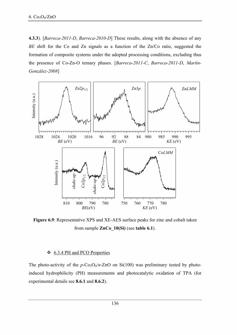
6. Co3O4/ZnO
136
4.3.3). [Barreca-2011-D, Barreca-2010-D] These results, along with the absence of any
BE shift for the Co and Zn signals as a function of the Zn/Co ratio, suggested the
formation of composite systems under the adopted processing conditions, excluding thus
the presence of Co-Zn-O ternary phases. [Barreca-2011-C, Barreca-2011-D, Martín-
González-2008]
Inte
nsit
y (a
.u.)
1028 1024 1020 1016BE (eV)
Zn2p3/2
96 92 88 84BE (eV)
Zn3p
995990985980KE (eV)
ZnLMM
780770760750KE (eV)
CoLMM
Inte
nsit
y (a
.u.)
810 800 790 780BE(eV)
Co2
p 1/2
shak
e-up
shak
e-up
Co2
p 3/2
Figure 6.9: Representative XPS and XE-AES surface peaks for zinc and cobalt taken
from sample ZnCo_10(Si) (see table 6.1).
6.3.4 PH and PCO Properties
The photo-activity of the p-Co3O4/n-ZnO on Si(100) was preliminary tested by photo-
induced hydrophilicity (PH) measurements and photocatalytic oxidation of TPA (for
experimental details see 8.6.1 and 8.6.2).

6. Co3O4/ZnO
137
Irradiation time (h)
120
110
100
90
80
70
60
50
400 5 10 15 20 25 30
Con
tact
ang
le (
°)
ZnCo_10(Si)
k
k1 ≈ 5· 10-9·mol-1 l-1 min-1150
100
50
0Con
cent
ratio
n H
TPA
(10
-9m
ol/l)
0 20 40 60 80 100Irradiation time (h)Irradiation time (h)
ZnCo_10(Si)ZnCo_60(Si)
Figure 6.10: (a) Water contact angle as a function of irradiation time obtained from
sample ZnCo_10(Si). (b) HOTPA concentration as a function of irradiation time taken
from samples ZnCo_60(Si) and ZnCo_10(Si). For sample assignments see table 6.1.
PH properties were analyzed by measuring the water contact angle as a function of the
UV irradiation time (figure 6.10 (a)). In the absence of UV light, the hydrophobic WCA
was close to 120°, as also observed for non-activated pure ZnO (3.4.5), [Barreca-2009-A,
Bekermann-2010-A] which can be explained by: (1) the relative rough composite surface;
[Barreca-2009-A] (2) the presence of aliphatic carbon, arising from surface
contamination (see XPS data). [Badre-2009, Barreca-2007-B, Bekermann-2010-A, Feng-
2004] Upon UV-light irradiation the WCA decreased, reaching half of its initial value
after four hours and a minimum value of 50° after five hours, indicating to an enhanced
surface wettability. [Feng-2004, Zhou-2008] The latter originates from the formation of
oxygen vacancies by the reaction of photo-generated holes with lattice O, ultimately
(a)
(b)

6. Co3O4/ZnO
138
resulting in the dissociative adsorption of H2O. [Barreca-2009-A, Bekermann-2010-A] It
is also worth noting, that upon prolonged UV irradiation the hydrophilic surface
properties were maintained for at least 24 hours, an interesting aspect in view of eventual
technological applications.
The self-cleaning activity of Co3O4/ZnO has been tested by the photocatalytic oxidation
of TPA to HOTPA (8.6.2). [Černigoj-2010] Consequently, the HOTPA concentration was
monitored as a function of the UV-irradiation time (figure 6.10 (b)). As a general rule, a
progressive increase with illumination time was observed, following a pseudo-zero-order
kinetics (rate constant = k1). The obtained data points could be fitted according to the
model introduced in paragraph 3.4.5, yielding a kinetic constant of k1 = 5·10-9 mol·l-1, a
value comparable to that of the bench mark material (Pilkington® Active glass).
[Bekermann-2010-A, Mills-2003]
Despite being prelimary, the present results demonstrate the potential of such
nanocomposites for self-cleaning and anti-fogging surfaces. [Kansal-2007, Kuo-2007,
Sun-2001]
6.3.5 Gas Sensing Properties
Investigation of the composite gas sensing performances was addressed at the detection of
acetone, ethanol and nitrogen dioxide, and selected dynamic responses are displayed in
figures 6.11 (a-c). (Technical details and definitions of responses, response and recovery
times can be found in paragraph 8.6.4.) As can be observed, the measured conductance
underwent an increase in the presence of reducing gases (CH3COCH3, CH3CH2OH,
figures 6.11 (a-b)), whereas the opposite phenomenon was revealed upon contact with
NO2, an oxidizing analyte (figure 6.11 (b)). Such a behavior, typical for n-type SCs,
[Barreca-2010-A, Hwang-2009] was related to the higher overall content of the ZnO
phase with respect to Co3O4 (see 6.3.2 and 6.3.3). Furthermore, for all the tested analytes
the conductance variation progressively increased with the gas concentration, enabling to
rule out appreciable saturation effects under the adopted conditions. The almost complete
recovery of the baseline conductance values at the end of each pulse indicated a reversible
interaction between the sensing element and the target analytes.

6. Co3O4/ZnO
139
The generally accepted sensing mechanism for similar SC systems is based on the initial
dissociative chemisorption of oxygen at the sensor surface, resulting in the formation of
negatively charged oxygen species (see also paragraph 3.4.6). [Barreca-2010-C,
Barreca-2010-A, Barreca-2011-C, Hwang-2009, Kim-2010, Na-2011] Upon adsorption
of CH3CH2OH or CH3COCH3, oxygen species promote their oxidation to CO2 and H2O
and the concomitant release of electrons into the system conduction band, increasing thus
the concentration of main charge carriers and, hence, the measured conductance. In a
different way, upon sensing of an oxidizing gas, such as NO2, electrons are withdrawn
from the SC surface, resulting in a conductance decrease. Irrespective of the target gas,
the sharp conductance variation observed on the analyte injection, followed by a slower
increase up to the end of the pulse, suggested that the analyte chemisorption was the rate-
determining step for the overall process. [Barreca-2010-C, Barreca-2011-A]
0
Response NO2
Response ethanolResponse acetone
10-7
10-6
1800 1850 1900 1950
CoZnO22A_L3(A) NO2(ppm)
10-7
10-6
10-5
10-4
1200 1250 1300 1350
CoZnO22A_L3(A) Acetone(ppm)
Con
duct
ance
(S)
Con
duct
ance
(S)
NO
2(ppm
) Res
pons
e
10-4
10-5
10-6
10-7
102
101
100
10-2
10-1
10-6
10-7
200
150
100
50
0
CH
3 CO
CH
3(ppm
)
10
8
6
2
4
0
10-7
10-6
10-5
10-4
650 700 750 800
CoZnO22A_L3(A) Ethanol(ppm)
CH
3 CH
2 OH
(ppm)
10-4
10-5
10-6
10-7
1000
800
600
200
400
0
CH3COCH3 (100 ppm)CH3CH2OH (500 ppm)NO2 (5 ppm)
1200 1250 1300 1350Time (min)
650 700 750 800
1800 1850 1900 1950 100 200 300 400Working temperature ( C)
Time (min)
Time (min)
(d)
(b)
(c)
(a)
Con
duct
ance
(S)
Figure 6.11: Gas sensing responses (black) of a Co3O4/ZnO sensor (ZnCo_10(Al), see
table 6.1 and figure 6.4) toward square concentration pulses (blue) of (a) CH3COCH3, (b)
CH3CH2OH, and (c) NO2. Working temperatures = (a, b) 400 and (c) 200 °C. (d)
Dependence of the response on the operating temperature for selected analyte
concentrations (specimen ZnCo_10(Al)).

6. Co3O4/ZnO
140
ZnCo_10(Al)
ZnCo_60(Al)
ZnCo_120(Al)
ZnCo_30(Al)
100
10
1
0.1
(a)
Res
pons
e
100
10
1
0.1
ZnCo_60(Al)
ZnCo_120(Al)
ZnCo_30(Al)
(b)ZnCo_10(Al)
Res
pons
e
2
1.5
1.0
0.5
0
ZnCo_10(Al)
ZnCo_60(Al)
ZnCo_120(Al)
ZnCo_30(Al)
(c)
Res
pons
e
Figure 6.12: Responses toward (a) 100 ppm CH3COCH3, (b) 500 ppm CH3CH2OH, and
(c) 5 ppm NO2 for nanocomposites characterized by a different Co3O4 deposition time
(see table 5.1). Working temperatures = (a, b) 400 and (c) 200 °C.
In view of practical applications, the sensor selectivity is a key concern and, at the same
time, an open problem still far from being completely solved. [Barreca-2011-A, Na-2011]
In the present work, the selectivity towards reducing or oxidizing gases could be
controlled as a function of the sensor working temperature (figure 6.11 (d)). Indeed, at
100°C the measured responses to NO2 (> 1) were higher than the corresponding values

6. Co3O4/ZnO
141
for CH3COCH3 and CH3CH2OH. Conversely, for working temperatures higher than
200°C, the response to nitrogen dioxide progressively lowered, and a net increase of the
responses to reducing gases was detected at 400°C, yielding values higher than 10. These
results are of interest in view of technological application of the current sensors in the
presence of gas mixtures under real-world conditions.
The responses of nanocomposites characterized by different Co3O4 deposition times
toward fixed concentrations of CH3COCH3, CH3CH2OH, and NO2 are displayed in figure
6.12. As can be observed, irrespective of the target analyte, the system performances
decreased on going from sample ZnCo_10(Al) to ZnCo_120(Al). This result can be
likely ascribed to the concurrence of two main factors, i.e. the increased Co3O4 particle
size and the partial reduction of the system porosity for the highest cobalt oxide loadings
(see also comments to figure 6.13). These findings indicate that the best performances
correspond to a Co/Zn ratio ensuring, at the same time, an efficient interfacial contact
between ZnO and Co3O4 and a high surface area available for gas adsorption.
substrate
ZnO
Co3O4
analyte
reduced particle size
p/n junctioneffects
catalyticactivity
Figure 6.13: Schematic representation of the main phenomena beneficially affecting the
gas sensing behaviour of the present Co3O4/ZnO nanocomposites.
In the case of specimen ZnCo_10(Al), where such conditions are likely fulfilled, the
sensor performances result appreciably better than those of our previous studies on pure,
Au-doped or F-doped Co3O4 (see also 4.4.6), [Barreca-2010-C, Barreca-2011-C] and
comparable to the results obtained by Na et al., [Na-2011] the only work on Co3O4/ZnO
gas sensors reported so far. Such results can be explained by considering that p-Co3O4/n-
ZnO junctions produce an improved charge separation at the interface between the two

6. Co3O4/ZnO
142
oxides, generating, in turn, an enhanced conductance modulation upon interaction with
the target gases (figure 6.13).
In this context, the reduced particle size and the well-known catalytic activity of cobalt
oxide are believed to play a further beneficial role on the functional behavior. [Na-2011]
It is worth observing that whereas n-type metal oxides only chemisorb as much oxygen as
necessary to compensate their deficiencies, the concentration of surface oxygen on p-type
SCs is significantly higher (see also 4.2). [Barreca-2011-C, Kim-2010] As a consequence,
the co-presence of Co3O4 and ZnO, with an intimate contact between them, can further
contribute to the improvement of the composite sensor performances.
10-3
10-4
Con
duct
ance
(S)
Con
duct
ance
(S)C
H3 C
OC
H3
(ppm)
CH
3 CH
2 OH
(ppm)
10-3
10-4
400 450 500 550 400 450 500 550Time (min) Time (min)
200
150
100
50
0
1000
800
600
400
200
0
Figure 6.14: Dynamic response (black) of a bare Co3O4 film towards square
concentration pulses (blue) of CH3COCH3 (a) and CH3CH2OH (b). Working temperature
= 400°C.
To validate the above observations, a bare Co3O4 film was grown directly on Al2O3
adopting the same synthesis conditions used for cobalt oxide in specimen ZnCo_10(Al).
As expected, upon exposure to reducing gases such as acetone or ethanol (see figure
6.14), Co3O4 displayed a conductance reduction, in line with its p-type behaviour.
[Barreca-2011-C] Apart from this difference with respect to sample ZnCo_10(Al), the
response values extrapolated by figure 6.14 were more than one order of magnitude
lower than the ones obtained for the corresponding Co3O4/ZnO composite under the same
testing conditions (see also figures 6.11 and 6.12). As previously discussed, these
findings highlight beneficial synergistic effects originating from Co3O4/ZnO coupling.
Similar results were also observed for the detection of NO2. In this case, whereas

6. Co3O4/ZnO
143
Co3O4/ZnO possessed a remarkable sensitivity for such analyte, bare Co3O4 displayed an
almost negligible response, in line with results presented in 4.4.6.
In the literature, ZnO deposits with thickness comparable to the zinc oxide layer of the
present Co3O4/ZnO nanocomposites have been reported to display gas sensing
performances both higher or lower that the ones reported above. [Al-Hardan-2010,
Barreca-2010-A, Kakati-2010, Trinh-2011] Such issue indicates that, beside film
thickness, gas sensing performances are also affected by other parameters (e.g., crystallite
size, surface area, defect content,...), evidencing thus the importance of both material
design and morphological/ structural control.
6.4 Conclusions
The work presented in this chapter was focused on the deposition of p-Co3O4/n-ZnO
nanocomposites by a two-step PECVD process, consisting in the growth of Co3O4
crystallites on the tips of 1D-like ZnO under relatively mild processing conditions (20 W,
200 – 300°C). An extensive characterization of the system structure, morphology and
composition unambiguously evidenced the co-existence of the two single-phase oxides
and an increasing Co3O4 overall loading on top of the ZnO with increasing Co3O4
deposition time. The obtained systems were highly pure and characterized by an intimate
Co3O4/ZnO contact.
Since such axial nanoheterostructures are promising candidates for the exploitation of the
p/n interface for potential functional applications, we tested the Co3O4/ZnO material in
PH and PCO, revealing activity for light-activated functional applications, such as
antifogging or self-cleaning materials. Despite being preliminary, the measured PCO
activities are competitive with the current bench mark material (Pilkington® Active glass).
Furthermore, tests of the alumina based composites in the detection of reducing
(CH3CH2OH, CH3COCH3) and oxidizing (NO2) gases revealed n-type behavior, due to
the higher overall content of the ZnO phase. Gas sensing interactions with all target
analytes were reversible, a key issue in view of eventual technological applications. The
sensing performances were dependent on the Co/Zn ratio, i.e. the interfacial contact
between ZnO and Co3O4 and the systems porosity. As a consequence, the best

6. Co3O4/ZnO
144
performances were obtained using ZnCo_10(Al), characterized by the lowest Co3O4
loading, being superior compared to pure, Au- or F-doped Co3O4 sensors (see also 4.4.6)
and comparable to the results obtained by Na et al., the only work on Co3O4/ZnO gas
sensors reported so far. [Na-2011] Such results can be attributed to the co-presence of
several beneficial phenomena: (i) the reduced particle size, enabling enhanced
conductance modulations upon interaction with the target analytes; (ii) p/n junction
effects at the Co3O4/ZnO interface, inducing an extension of the electron depletion layer;
(iii) the Co3O4 catalytic activity, promoting the chemical reactions taking place during the
sensing process.
Overall, the growth strategy adapted in this work paves the way to fabricate metal oxide
nanocomposites with axial alignment under mild processing conditions and opens
intriguing perspectives for the design of p/n composite nanoarchitectures for different
kinds of applications, from heterogeneous catalysis to photo-induced pollutant
degradation and ferromagnets in spintronic devices.

7. Summary and Perspectives
145
7. Summary and Perspectives
This PhD thesis has been devoted to the development of innovative vapor-phase routes to
the synthesis of multifunctional metal oxide nanostructures.
In particular, the attention has been devoted to the use of Chemical Vapor Deposition
processes (CVD, PECVD), versatile means for the obtainment of nanosystems with
tailored features. The most attractive characteristics of such techniques are the possibility
of obtaining a conformal coverage of complex-shaped substrates and of achieving pre-
scribed material features by a proper choice of the precursor compound and its activation
pathway. In this context, PECVD enables to obtain supported nanomaterials under mild
conditions thanks to the unique features of non-equilibrium plasmas. Furthermore, the
concurrence between growth and ablation, as well as electric field effects, offer peculiar
degrees of freedoms in the tailoring of metal oxide systems.
Another promising vapor-phase process is sputtering, enabling the bottom-up synthesis of
nanostructures with well defined composition and at low substrate temperatures, down
even to the room one. These characteristics, in combination with a high infiltration power,
candidate sputtering as an amenable route for the development of hybrid processes in the
synthesis of composite materials.
Basing on the above considerations, the main aim of the thesis was the development of
versatile synthesis procedures for the obtainment of multifunctional zinc and cobalt oxide
based nanostructures by CVD, PECVD, sputtering and their synergistic combinations. A
relevant part of research efforts has been devoted to the synthesis and characterization of
suitable metal organic precursors, endowed with high volatility and clean decomposition
patterns, as required for CVD application. Composition, morphology, microstructure and
optical properties of the obtained nanosystems were investigated by means of a multi-
technique approach, involving FE-SEM, AFM, GIXRD, (HR)TEM, EDXS, RBS,
XPS/XE-AES, SIMS, FT-IR, UV-Vis and PL measurements. Functional validation was
aimed at investigating the material functional performances in:
- energetics, with particular regard to light-induced H2 production from aqueous
solutions;
- photo-induced hydrophilicity and photocatalytic performances in pollutant oxidation;
- gas sensing of flammable/toxic gases.
The key results of the research activity are briefly summed up in the following.

7. Summary and Perspectives
146
Zinc Oxide Nanostructures (Chapter 3)
The two novel volatile bis(ketoiminato) zinc compounds with clean decomposition
pattern, [Zn{[(CH2)xOCH3]NC(CH3)=C(H)C(CH3)=O}2] (1: x = 2; 2: x = 3), have been
tested in the thermal CVD of ZnO, yielding very pure and <001> oriented ZnO films of
high crystalline quality. Encouraged by these results and in order to achieve a better
control of the ZnO nanostructure growth at lowered deposition temperatures, PECVD
using 1 and 2 was carried out. Pure and strongly <001> oriented ZnO nanorod arrays with
a tailored spatial organization have been grown in Ar/O2 plasmas under mild conditions
(optimal 200 - 300°C). These results have been attributed to the beneficial effects arising
from cold plasma activation, that enabled a fine-tuning of the system structure and
morphology, from continuous films to oriented nanorods. This control had a key
importance for the PSH and PCO properties of Si(100) supported NR arrays, since a
direct dependence of the performances on the ZnO structure and morphology was
observed. The highest PSH and PCO activity was obtained for long and sparse ZnO
nanorods, exhibiting a high surface area and enabling an improved light trapping.
3D-1D urchin-like structures were obtained upon depositing ZnO NR arrays on
polycrystalline Al2O3 substrates, and their potential for the detection of various oxidizing
and reducing gases has been studied. Very high responses were obtained, along with the
possibility to discriminate between reducing and oxidizing gases as a function of the
operation temperature. These promising features were related to the high surface-to-
volume ratio of the urchin-like ZnO and to their reduced lateral dimensions, enabling
improved conductance modulation upon interaction with the analytes.
Co3O4 (Chapter 4)
Pure and fluorine-doped Co3O4 nanodeposits were obtained by the PECVD from
[Co(dpm)2] (3) and [Co(hfa)2·TMEDA] (4) in Ar/O2 plasmas at temperatures from 100 –
400°C. The use of 3 and 4 as CVD Co sources was motivated by their air-stability,
volatility and clean decomposition pattern. A proper choice of the PECVD processing
parameters allowed to synthesize Co3O4-based nanomaterials with tailored properties on
diverse substrates.
In particular, pure and strongly oriented Co3O4 thin films were grown on MgO(100) and
MgAl2O4(100) at temperatures as low as 100°C, an outstanding results, since the

7. Summary and Perspectives
147
synthesis of expitaxial/strongly oriented usually involves harsh conditions in terms of
energy supply.
This successful synthesis strategy was further adopted for the growth of Co3O4 on Si(100)
and Al2O3 substrates, in view of their functional tailoring for photocatalytic H2 generation
and gas sensing applications, respectively. In this context, key efforts were dedicated to
F-doping and its impact on the physico-chemical and functional features of Co3O4. In
fact, the use of [Co(hfa)2·TMEDA] (4) in the plasma process led to the generation of
fluorine radicals and thus allowed to achieve a homogeneous and controllable fluorine-
doping of the Co3O4 systems.
Interestingly, UV-Vis measurements showed that the fluorine incorporation led to an
increase of the absorption coefficient and to a 5-fold activity increase in photocatalytic H2
generation under UV illumination. These improved performances with respect to pure
Co3O4 were ascribed to an enhanced light absorption and the role of F as a passivation
agent, resulting in a reduced carrier trapping.
As regards gas sensing, F-Co3O4 yielded higher responses for the detection of acetone and
ethanol than the corresponding pure Co3O4 specimens. In addition, fluorine-introduction
led to enhanced responses and higher reversibility of the sensing processes, as well as to
decreased working temperature. The observed attractive sensing properties of F-Co3O4
were mainly related to an enhanced Lewis acidity of Co surface sites, promoting the
system catalytic activity.
Ag/ZnO (Chapter 5)
An innovative plasma-assisted route for the growth and functional tailoring of Ag/ZnO
nanocomposites has been presented, based on ZnO NR synthesis by PECVD (chapter 3)
and the subsequent over-dispersion of different Ag amounts by variation of the sputtering
time. Under mild conditions a high dispersion of Ag nanoparticles on the ZnO matrices
was achieved. In particular, the Ag NPs distribution and size could be controlled as a
function of the sputtering time and post-annealing, the latter also affecting Ag(0)-Ag(I)
inter-conversion.
The physico-chemical features of the Ag/ZnO systems had a direct impact on the
functional performances. In the photocatalytic H2 generation by photo-reforming, the use
of the Ag/ZnO materials resulted in very promising and stable responses under both UV

7. Summary and Perspectives
148
and Vis irradiation, whereas pure ZnO was not active. This behaviour, enabled by the
intimate Ag/ZnO contact was related to the formation of Ag/ZnO Schottky or Ag2O-ZnO
p/n junctions, improving charge carrier separation. Further contributions arose from the
co-presence of Ag(0)-Ag(I), the latter possessing a favourable catalytic activity. For the
H2 detection, Ag loading on ZnO NR arrays, led to very high responses without any
saturation at moderate operation temperatures (200°C). These attractive performances
were related to the synergy of the peculiar ZnO morphology with the catalytic properties
of Ag NPs.
Overall, by the combined approach of PECVD and sputtering multifunctional platforms
for the sustainable generation and sensing of hydrogen were both prepared and operated
under mild conditions, beneficial in terms of cost- and energy dissipitation.
Co3O4/ZnO (Chapter 6)
A novel two-step PECVD synthesis has been developed for the growth of Si(100) and
Al2O3 supported p-Co3O4/n-ZnO nanocomposites, consisting of the PECVD of ZnO NR
arrays followed by over-growth of Co3O4 from [Co(dpm)2] (3) at 200°C in Ar/O2
plasmas. The Co3O4 loading was varied as a function of its deposition time (10 min – 120
min). The composite morphological, structural and compositional evolution with
increasing Co3O4 loading, i.e. deposition time, were systematically investigated. The co-
existence of both single-phase oxides with a close contact of Co3O4 grains with the
underlying ZnO matrices, were clearly evidenced.
Preliminary PH and PCO studies showed a change of the surface properties from
hydrophobic to hydrophilic upon UV irradiation, with a stable hydrophilicity for at least
24 hours. Furthermore, the activity of the Co3O4/ZnO materials in the photo-activated
oxidation of TPA was competitive to that of the bench-mark Pilkingtion® material. As
regards gas detection, Co3O4/ZnO showed to be sensitive towards reducing and oxidizing
analytes, namely CH3CH2OH, CH3COCH3 and NO2, and a certain selectivity depending
on the working temperature, has been observed. These promising functional properties
can be traced back to a reduced particle size, p/n junction effects at Co3O4/ZnO interfaces
and the catalytic activity by Co3O4.

7. Summary and Perspectives
149
Due to the encouraging results, more detailed investigations of the Co3O4/ZnO structure
(TEM) and systematic studies on the interrelationships between the composite physico-
chemical properties and functional behaviour will be undertaken
Perspectives
In conclusion, the presented work has concerned the development of oxide nanomaterials
as multifunctional platforms by innovative vapour-phase routes. The unique versatility of
the adopted approaches will enable to transfer the presented synthesis strategies for the
growth of different metal oxide systems (like FexOy/ZnO, FexOy/Co3O4, ...), as well as
their modification by doping or composite formation. In particular, the possibility of in-
situ anion-doping in PECVD will be further exploited, one near aim being the fluorine-
doping of ZnO by use of [Zn(hfa)2·TMEDA], for the subsequent development FexOy/F-
ZnO systems. Using sputtering processes, it is also planned to functionalize the obtained
systems with metal particles (Cu, Ag, Au,...). In this regard, the attention will be devoted
to obtain improved performances in sensing and photo-activated applications, but also to
design of nano-electrodes to be integrated into lithium-ion batteries.

8. Experimental
150
8. Experimental
In this chapter, synthesis and characterization of the metal organic compounds 1 - 4, and
the deposition experiments along with the reactor set-ups are presented. Basic principles
and experimental details of the analysis methods used for the characterization of the
precursors and nanodeposits are also provided. Paragraphs 8.1 and 8.2 deal with the
syntheses of the zinc and cobalt precursors, respectively. Since the metal organic
compounds play a crucial rule in CVD processes, their composition, structure, thermal
properties and fragmentation patterns have been investigated. The corresponding results
are briefly discussed in paragraph 8.1 and 8.2. The set-ups of the CVD and sputtering
instruments are presented in paragraph 8.3, and an overview of all depositions
performed in this thesis is given. In paragraph 8.4, precursor characterization techniques
are described. The obtained nano materials were analyzed by a combination of advanced
characterization techniques with respect to their morphology, composition, structure and
optical properties (paragraph 8.5). In paragraph 8.6, the experimental details of the
functional characterizations performed are provided. In particular, photo-induced
superhydrophilicity, photocatalytic oxidation, photocatalytic H2 production and gas
sensing behaviour were investigated.
8.1 Synthesis and Characterization of Bis(ketoiminato)zinc (II) Complexes
1 and 2
8.1.1 Synthesis of 1 and 2
The zinc ketoiminates were obtained by the stoichiometric reaction of DEZ with the
neutral ketoiminate in hexane (scheme 8.1). Compounds 1 and 2 were characterized by
EA, 1H-NMR and 13C-NMR spectroscopy, Single Crystal X-ray Diffraction and EI-MS.
[Bekermann-2010-C] As both the compounds are very similar (with a small change in the
ligand skeleton), the synthesis procedure, structural, and precursor properties of
[Zn{[(CH2)2OCH3]NC(CH3)=C(H)C(CH3)=O}2] (1) will be discussed in detail as a
representative example.
All manipulations of air- and moisture-sensitive compounds were performed in a
conventional vacuum/argon line by using standard Schlenk techniques. Pure DEZ was
purchased from ABCR and used as received. Preparations of samples for further analysis

8. Experimental
151
were carried out in argon-filled glove boxes (MBraun, Lab-Master). All solvents were
purified by an MBraun solvent purification system and stored over molecular sieves (4
Å).
(reaction 8.1)
Scheme 8.1: Reaction scheme for the synthesis of 1 and 2.
For the synthesis of 1, DEZ (3 ml, 29.39 mmol) was dissolved in dry hexane (150 ml).
The solution was stirred for 12 h and cooled down to –15°C. To this mixture
(CH3OCH2CH2)N(H)C(CH3)=C(H)C(CH3)=O (7.11 ml, 58.78 mmol) was added by
syringe. The reaction was heated at reflux for 1.5 h and afterwards stirred for 12 h at
room temperature. The solvent was removed in vacuo at room temperature. The solid
residue was washed with dry pentane (3 × 5 ml) and dried again. The product was
obtained as a light yellow powder (8.81 g, 23.43 mmol, 79.7 %). Its chemical
composition was determined to be C 51.02, H 7.48, N 7.48 by EA, as theoretically
expected for the sum formula C16H28N2O4Zn (377.80) (C 51.07, H 7.45, N 7.45). The
synthesis procedure of 2 was similar to that adopted for 1. DEZ (3 ml, 29.39 mmol) was
treated with (CH3OCH2CH2CH2)N(H)C(CH3)=C(H)C(CH3)=O (7.68 ml, 58.78 mmol).
The product C18H32N2O4Zn (405.85) was obtained as a light-yellow powder (8.00 g,
19.80 mmol, 67.3 %) and had the composition C 53.51, H 7.93, N 6.86 (calculated: C
53.47, H 7.92, N 6.93).
8.1.2 NMR of 1 and 2
In the 1H-NMR of compound 1 (figure 8.1), the two singlets at δ = 1.57 and 1.97 ppm
correspond to the methyl groups attached to the chelate ring, whereas those shifted low
field to δ = 3.05 ppm can be attributed to the methyl group of the ether arm. The singlet at
δ = 4.78 ppm corresponding to one proton can be attributed to the hydrogen atom at the
chelate ring. At δ = 3.25 and 3.46 ppm two broad signals appear with an integration
ONH
R
Et2Zn
hexane, 0°C
Zn
N OR
1: R= O(CH2)2CH32: R= O(CH2)3CH3
NO
R
2 + 2 C2H5

8. Experimental
152
corresponding to four protons; these signals are assigned to the ether side chain. Below,
tables of all NMR signals can be found.
Figure 8.1: 1H NMR of 1.
Table 8.1: NMR data of 1.
1H NMR (250 MHz, C6D6, 25 °C) 13C NMR (100.6 MHz, C6D6, 25 °C)
Table 8.2: NMR data of 2.
1H NMR (250 MHz, C6D6, 25 °C) 13C NMR (100.6 MHz, C6D6, 25 °C)
(ppm) 6.0 5.0 4.0 3.0 2.0 1.0
4.78
3.46
3.25
3.05
1.97 1.57
δ [ppm] attribution
1.61 s 3 H -NC(CH3)
1.86 quint. 2 H NCH2CH2CH2OCH3
2.01 s 3 H -OC(CH3)
3.02 s 3 H N(CH2)3OCH3
3.16 t 2 H NCH2CH2CH2OCH3
3.32 t 2 H NCH2CH2CH2OCH3
4.80 s 1 H OC(CH3)C(H)C(CH3)N
δ [ppm] attribution
1.57 s 3 H -NC(CH3)
1.97 s 3 H -OC(CH3)
3.05 s 3 H N(CH2)2OCH3
3.25 and 3.46 2 m 4 H -N(CH2)2CH3
4.78 s 1 H OC(CH3)C(H)C(CH3)N
δ [ppm] attribution
22.02 NC(CH3)
27.84 OC(CH3)
50.51 N(CH2)2O(CH3)
58.45 N(CH2)2O(CH3)
96.87 OC(CH3)C(H)C(CH3)N
172.48 OC(CH3)C(H)C(CH3)N
183.47 OC(CH3)C(H)C(CH3)N
δ [ppm] attribution
21.40 NC(CH3)
27.77 OC(CH3)
31.36 NCH2CH2CH2OCH3
48.06 NCH2CH2CH2OCH3
58.15 N(CH2)3O(CH3)
70.17 NCH2CH2CH2OCH3
96.87 OC(CH3)C(H)C(CH3)N
172.48 OC(CH3)C(H)C(CH3)N
183.47 OC(CH3)C(H)C(CH3)N

8. Experimental
153
8.1.3 Single Crystal X-ray Diffraction of 1
Figure 8.2: Molecular structure of 1 (see also reaction 8.1). Hydrogen atoms are removed
for clarity. Ellipsoids are shown with 50 % of probability level.
Single crystals of 1 suitable for X-ray structural analysis were obtained from a saturated
solution of the compound in toluene at –30°C over a period of 24 h. Molecule 1
crystallizes in the orthorhombic space group Pca21. The solid state structure of 1 with an
atom-numbering scheme is shown in figure 8.2. Molecule 1 is a monomer and it consists
of a distorted tetrahedral Zn center with two bidentate ketoiminate ligands. The
coordination environment around the zinc is completed by the oxygen and nitrogen atoms
of two ketoiminato ligands orthogonal to each other. The six-membered ZnONC3 units
are puckered. The oxygen atoms (O3 and O4) of Me–O–CH2–CH2–N are far away from
the coordination sphere of the zinc center. The crystal structure indicates that the
electrons are not completely delocalized in the six membered ring, for the following
reasons: (i) The bite angles of the chelating ligands are 97.3 and 97.1°, respectively, and
the angles O2–Zn1–N1, O1–Zn1–N2, O1–Zn1–O2, and N1–Zn1–N2 vary between 108.5
and 125.4°, deviating from those expected for an ideal tetrahedron. (ii) As expected, the
Zn–O bonds with lengths of 1.955 and 1.939 Å are longer than those for the Zn–N bonds
[1.990(2) Å and 1.984(2) Å]. (iii) The torsion angles indicate a non-planar six-membered
ring. For a more detailed description of the crystal structure, crystal and structure
refinement data see [Bekermann-2010-C].
Zn1N1
C9
C10
O3
C11
N2
O2
O1
O4
C2
C7
C1
C8
C4C5
C12
C6
C13 C14
C15
C16
C3

8. Experimental
154
8.1.4 EI-MS of 1 and 2
The fragmentation mechanism of the bis(ketoiminato) precursors 1 and 2 was examined
by EI-MS (table 8.3). Both compounds were clearly identified by their M+· signals at m/z
= 376 and 404 for 1 and 2, respectively. Typical primary fragments were generated by the
cleavage of methyl or ether groups from the remaining chelating ring. All recorded mass
spectra strongly supported the complete cleavage of the whole ligand under EI-MS
conditions. The decomposition pattern gave no evidence due to formation of fragments,
containing Zn-C bonds, thus indicating, that the precursors might not incorporate C upon
their use in ZnO CVD.
Table 8.3: EI-MS data for 1 and 2.
1 mass relative intensity 2 mass relative intensityfragments [ m /z ] [ % ] fragments [ m /z ] [ % ]
M+ · 376 2.0 M+ · 404 13.8
M+ · - CH3· 361 1.6 M+ · - CH3
· 389 2.0
M+ · - OCH3· 345 9.8 M+ · - OCH3
· 373 0.3
361 - C2H6 or - CH2O· 331 13.8 M+ · - C3H5· 363 1.0
or M+ · - CH2OCH3· M+ · - 58 346 1.0
M+ · - 1 ligand 220 100 M+ · - 1 ligand 234 100
OC3H6· or NC3H8 58
8.1.5 Thermal Characterization of 1 and 2
The melting points of 1 and 2 are 57 and 60°C, respectively. Both 1 and 2 can be
quantitatively vaporized at 110 and 115°C, respectively, at 5 mbar, without any
decomposition. Thermal analysis reveals a nearly one-step decomposition for both
compounds (figure 8.3), which is desirable for CVD precursors. The temperature window
between vaporization and decomposition is sufficiently large. The onset of volatilization
for 1 is at 70°C, whereas in the case of 2 it is at 90°C. For 1, a strong mass loss occurs
between 130 and 280°C, whereas the main mass loss for compound 2 starts around
150°C. This shows that a marginal variation in the ligand structure has a distinct influence
on the volatilization temperature. The sublimation behavior of the ketoiminato precursors
was further investigated by isothermal TG experiments carried out at 120 and 140°C. In
all cases, a linear weight loss was observed (figure 8.3), indicating that the precursors can

8. Experimental
155
sublime at the set temperature with constant rates for a long period of time. The
sublimation rates at 120°C were determined to be 9.3 μg min–1
for 1 and 20.1 μg min–1
for
2. The linear trends in the isothermal curves show clean vaporization processes with no
signs of premature decomposition.
100
weig
ht
(%)
60
70
80
90
400 600
t (min)
200
1 (120 C)
2 (120 C)
1 (140 C)
2 (140 C)
a)
b)
c)
d)
d)
c)
b)
a)
T ( C)
0 100 200 300 400
100
80
60
40
20
weig
ht
(%)
1
2
0
4.3 %
Figure 8.3: Thermal analysis of 1 and 2. Top: TG (5 K min–1
, 300 ml min–1
); bottom:
isothermal vaporization studies of 1 and 2 at two different temperatures.
8.2 Synthesis and Characterization of [Co(dpm)2] (3) and
[Co(hfa)2·TMEDA] (4)
8.2.1 Synthesis of 3 and 4
Both precursors, [Co(dpm)2] (3) and [Co(hfa)2·TMEDA] (4), have already been reported
and were synthesized according to the corresponding literature procedures. [Bandoli-
2009, Barreca-2001] In order to gain a more thorough insight into their fragmentation
and thermal properties, EI-MS and isothermal TG studies were carried out, prior to their
use in PECVD.

8. Experimental
156
8.2.2 EI-MS of 3 and 4
Precursors 3 and 4 were characterized by EI-MS, since the ionization conditions used for
EI-MS analyses are analogous to those adopted in PECVD processes. Thus it is
reasonable to suppose that a similar fragmentation process also occurred during the
plasma-assisted growth of Co3O4-based systems, explaining the effective fluorine-
incorporation into the deposited material (see paragraph 4.4.3).
In the case of [Co(dpm)2], the EI-MS spectrum (figure 8.4) was dominated by several
species originating from the loss of the β-diketonate ligand and of the tert-butyl group,
whose presence was also directly detected. [Barreca-2001] For [Co(hfa)2·TMEDA]
(figure 8.4), the detachment and fragmentation of both the TMEDA and hfa moieties
were revealed. In particular, ions containing the β-diketonate ligand were involved in the
elimination of CF2/CF3 species, whose formation was in agreement with compositional
data on Co3O4 based deposits (see [Gasparotto-2011-A] and paragraph 4.4.3). A careful
analysis of EI-MS results also revealed a mass loss of 19 a.m.u. from several ionic species
(see for instance m/z = 589 → 570; m/z = 473 → 454). These results pointed out to the
formation of fluorine radicals, accounting for the efficient Co3O4 fluorine-doping under
the present PECVD conditions.

8. Experimental
157
.
Figure 8.4: EI-MS spectrum of precursors 3 and 4. The assignment of the main peaks is
reported in the tables, where the symbol L indicated the dpm or the hfa ligand,
respectively. The structure of the molecular ions is also sketched.
m/z peak assignment
425 [CoL2]+·
368 [CoL2 – (CH3)3C]+
242 [CoL]+·
184 [HL]+·
127 [HL – (CH3)3C]+
57 [(CH3)3C]+
28 [CO]+·
425
O
O O
O
Co
m/z peak assignment
589 [CoL2·TMEDA]+·
473 [CoL2]+·
404 [CoL2 - CF3]+
382 [CoL·TMEDA]+
266 [CoL]+
216 [(CoL) – (CF2)]+·
116 [TMEDA]+·
69 [CF3]+
58 [CH2=N(CH3)2]+
Co
O
O
O
O
N
N
CF3
F3C
CF3
CF3
589

8. Experimental
158
8.2.3 Thermal Characterization of 3 and 4
The vaporization behaviours of 3 and 4 were further investigated by isothermal TG
experiments. Both precursors revealed a linear weight loss at the set temperatures, 90 and
120°C (figure 8.5), indicating that they can sublime with constant rates for a long period
of time. The vaporization rates at 90 °C (120 °C) were estimated to be 0.2 μg min–1 (2.9
μg min–1) for 3 and 13.6 μg min–1 (100.0 μg min–1) for 4. The linear trends in the
isothermal curves indicate clean vaporization processes with no signs of premature
decomposition, a key point in view of the eventual compound applications in CVD and
PECVD processes.
100 200 300 400 500 600 700
0,4
0,5
0,6
0,7
0,8
0,9
1,0
90°C 120°C
we
ight
(%
)
time (min)
Codpm2
90°C120°C
Co(dpm)21.0
0.9
0.8
0.7
0.6
0.5
0.4
Wei
ght (
%)
0 100 200 300 400 500 600 700 Time (min)
100 200 300 400 500 600 700
0,0
0,2
0,4
0,6
0,8
1,0 Co(hfa2)*TMEDA
90°C 120°C
wei
ght (
%)
time (min)
90°C120°C
Co(hfa)2·TMEDA
0 100 200 300 400 500 600 700
Time (min)
1.0
0.8
0.6
0.4
0.2
0
Wei
ght (
%)
Figure 8.5: Isothermal vaporization studies of 3 and 4 at two different temperatures.
8.3 Reactor Set-ups and Applied Deposition Parameters
8.3.1 CVD Reactor Set-up
The self-built horizontal cold wall reactor used in this work is shown in figure 8.6. It is
made up of a quartz tube, which is surrounded by a hollow glass cylinder, serving as

8. Experimental
159
cooling mantle. In the inner quartz tube a horizontally placed graphite susceptor is
inductively heated by high frequency. The substrate is positioned on a Si/C susceptor.
Substrate temperature is measured by a pyrometer focused on its surface. The
decomposition products are trapped into a nitrogen-cooled glass container. Beyond the
cooling trap there are two pressure gauges and an electronic needle valve. The rotary
pump serves as forepump for the turbo molecular pump (TMP). An electronic needle
valve, connected to pressure readers, is positioned in front of the TMP to control the
reactor pressure during deposition.
TMP Rotary pump
MFCMFCCooling trap
Water
Coil
(inductive heating)
Substrate
on susceptor
Pressure gauge
UHV
Pressure gauge
Electronic
needle valve
Heating bath
Reactive
gas
Carrier
gas
Figure 8.6: Scheme of the CVD reactor used (Ruhr-University Bochum).
The bubblers are u-form type glass tubes that are connected to the CVD system by two
flanges. The carrier gas flow is led through the bubbler, taking the precursor gas into the
reactor. The bubbler is heated by an air bath, and the temperature can directly be
measured on the bubbler itself. The lines between air bath and reactor are heated by
heating tapes to avoid precursor condensation. The system has a bypass through which
direct introduction of a reactive gas into the deposition chamber is possible. All gas flows
are controlled by mass flow controllers (MFCs). For the deposition of zinc oxide films,
electronic grade nitrogen and oxygen were used as carrier gas and reactive gas,
respectively.
Prior to each deposition, the substrates were ultrasonically cleaned in ethanol (10 min),
distilled water (10 min), and dried in air. At the beginning of each deposition experiment
the whole system was evacuated for one hour at 10-5 mbar to ensure removal of residual
gases.

8. Experimental
160
8.3.2 Deposition Parameters for CVD of ZnO (3.3.1)
Deposition of ZnO from [Zn{[(CH2)xOCH3]NC(CH3)=C(H)C(CH3)=O}2] (1: x = 2; 2: x =
3) was carried out using the self-built CVD reactor described in 8.3.1. Total pressure (p),
deposition time (t), N2 and O2 flow rates and vaporization temperature (Tvap) were
maintained at 10.0 mbar, 90 min, 50 sccm and 130°C. The investigated range of substrate
temperature (T) was 400 - 700°C. Table 8.4 lists all applied deposition parameters. For
sample indexing see paragraph 3.3.1.
Table 8.4: Deposition parameters for CVD of ZnO from 1 and 2. For sample indexing see
paragraph 3.3.1.
Material ZnO Paragraph 3.3.1
Precursor [Zn{[(CH2)xOCH3]NC(CH3)=C(H)C(CH3)=O}2]
(1: x = 2; 2: x = 3) Precursor amount 0.15 g
Tvap 130°C
Substrate Si(100), borosilicate
T 400 – 700°C
N2 flow rate 50 sccm
O2 flow rate 50 sccm
p 10 mbar t 90 min
8.3.3 Plasma Reactor Set-up
For the PECVD experiments performed in the framework of this thesis, a two-electrode
custom-built apparatus was used. [Barreca-2003-A] The instrumental set-up is sketched
in figure 8.7. The apparatus, equipped with both rotary pump and TMP, consisted of a
vacuum metal chamber with a first electrode powered by an RF generator and a second
one electrically grounded, to which the substrates were fixed with metallic clips. In each
experiment, the ground electrode was resistively heated and its temperature was measured
by a thermocouple. The diameter of each electrode was 9 cm and the inter-electrode
distance was fixed at 6 cm. Prior to each deposition, the system was evacuated to a base
pressure lower than 10-5 mbar, as measured by an inverted magnetron gauge. Flow rate

8. Experimental
161
values were controlled by flowmeters with ±1 sccm accuracy, whereas the deposition
pressure was monitored by barocel-capacitance manometers. A RF generator is connected
to one of the parallel electrodes, the RF electrode, by a matching system, while the second
electrode serves as ground electrode (figure 8.7). The matching system, basically a
condensator of tunable capacity, serves to optimize the energy transfer to the plasma,
minimizing the reflected power.
Heatingbath
Precurosr
Heater andtemperature
measurement
Matchingbox
RFgenerator
TMP
Cooling trap
PP
PLASMA
MFC Gas supply
MFC
Gas supply
RF electrode Groundelectrode
Reaction chamber
SubstrateBubbler
Gas lineby-pass
= Pressure readers
Rotary pump
P
P
Figure 8.7: Representative scheme of the PECVD reactor used (Padova University).
Depositions were performed on p-type Si(100) substrates and polycrystalline Al2O3
slides. The former were cleaned without removing the native oxide layer, by iterative
dipping in sulfonic detergent and distilled water, distilled water, acetone, and isopropylic
alcohol. [Armelao-1998] The Al2O3 substrates were cleaned in dichloromethane and
isopropanol by ultrasonification. Electronic grade Ar and O2 were used as plasma sources.
The precursor was placed in an external vessel heated by an oil bath and transported
towards the deposition zone by an Ar flow. Two further auxiliary gas-lines were used to
introduce Ar and O2 gases directly into the reactor. To avoid undesired condensation
phenomena, the gas lines connecting the precursor vessel and reaction chamber were
heated.

8. Experimental
162
Silver sputtering on ZnO deposits was carried out in the same plasma reactor, used for
PECVD, described in this paragraph. The supported ZnO specimen and silver source
were fixed on the ground electrode and RF electrode, respectively.
8.3.4 Deposition Parameters for PECVD of ZnO (3.4.1)
Depositions of ZnO from [Zn{[(CH2)xOCH3]NC(CH3)=C(H)C(CH3)=O}2] (1: x = 2; 2: x
= 3) were carried out using the PECVD reactor described in 8.3.3. Total pressure,
deposition time, vaporization temperature, Ar (carrier) and Ar/O2 flow rates were
maintained at 1.0 mbar, 60 min, 140°C, 60 and 20/15 sccm. The ZnO systems have been
studied as a function of precursor, substrate temperature and RF-power (P) used (table
8.5). For sample indexing see paragraph 3.4.1.
The ZnO matrices used for the composite materials (see paragraphs 5.3.1 and 6.3.1)
were grown under optimized conditions (table 8.5).
Table 8.5: Deposition parameters for PECVD of ZnO from 1 and 2. For sample indexing
see the corresponding paragraphs assigned in this table.
Material ZnO ZnO for Ag/ZnO
ZnO for Co3O4/ZnO
Paragraph 3.4.1 5.3.1 6.3.1
Precursor 1 2 2
Precursor amount 0.3 g 0.3 g
Tvap 140°C 150°C
Substrate Si(100), Al2O3 Si(100), Al2O3
T 100 – 400°C 300°C
P 10 – 40 W 20 W 20 W
Ar (carrier) flow rate 60 sccm 60 sccm
Ar/O2 flow rate 15/20 sccm 15/20 sccm
p 1 mbar 1 mbar
t 60 min 60 min

8. Experimental
163
8.3.5 Deposition Parameters for PECVD of Co3O4 (4.3.1 and 4.4.1)
Depositions of Co3O4 from [Co(dpm)2] (3) and [Co(hfa)2·TMEDA] (4) were carried out
using the PECVD reactor described in 8.3.3. Total pressure, RF-power, deposition time,
Tvap(3), Tvap(4), Ar (carrier) and Ar/O2 flow rates were maintained at 1.0 mbar, 20 W, 60
min, 90°C, 60°C, 60 and 20/15 sccm. The Co3O4 systems have been studied as a function
of substrate and deposition temperature in 4.3.1 (table 8.6). In 4.4.1, the influence of
precursor and substrate temperature (table 8.6) on the morphology and composition of
the (F-)Co3O4 deposits were investigated. For sample indexing see 4.3.1 and 4.4.1.
Table 8.6: Deposition parameters for PECVD of Co3O4 from 3 and 4. For sample
indexing see the corresponding paragraphs assigned in this table.
Material Co3O4 (F-)Co3O4 Paragraph 4.3.1 4.4.1
Precursor 3 3 4
Precursor amount 0.3 g 0.3 g
Tvap 90°C 90°C 60°C
Substrate Mg(100),
MgAl2O4(100) Si(100), Al2O3
T 100 – 400°C 100 – 400°C
P 20 W 20 W
Ar (carrier) flow rate 60 sccm 60 sccm
Ar/O2 flow rate 15/20 sccm 15/20 sccm
p 1 mbar 1 mbar
t 60 min 60 min
8.3.6 Deposition Parameters for PECVD/Sputtering of Ag/ZnO (5.3.1)
Initial PECVD of ZnO (from 2) and subsequent sputtering of Ag were carried out using
the plasma reactor described in 8.3.3. Based on studies presented in paragraph 3.4, the
ZnO matrices were grown under optimized condition (see table 8.5). Sputtering of Ag
was performed at p = 0.3 mbar, P = 5 W, T = 60°C and Ar flow rates of 10 sccm. The
Ag/ZnO systems have been studied as a function of silver sputtering time and annealing
(see table 8.7). For sample indexing see 5.3.1.

8. Experimental
164
Table 8.7: Parameters for sputtering of Ag on ZnO (see table 8.5 and 5.3.1).
Material Ag for Ag/ZnO Paragraph 5.3.1
Target Ag
Substrate ZnO/Si(100), ZnO/Al2O3
T 60°C
P 5 W
Ar flow rate 10 sccm
p 0.3 mbar
t 10 - 150 min
Annealing 400°C in air
8.3.7 Deposition Parameters for PECVD of Co3O4/ZnO (6.3.1)
Depositions of Co3O4/ZnO from precursors 2 and 3 were performed using the PECVD
reactor described in 8.3.3. Based on studies presented in paragraph 3.4, the ZnO
matrices were grown under optimized condition (see table 8.5). Subsequently, Co3O4 was
grown at p = 1 mbar, P = 20 W, T = 200°C, Tvap(3) = 100°C and Ar (carrier) and Ar/O2
flow rates of 60 and 20/15 sccm. The Co3O4/ZnO systems have been studied as a function
of Co3O4 deposition time (see table 8.8). For sample indexing see 6.3.1.
Table 8.8: Deposition parameters for PECVD of Co3O4 on ZnO (see table 8.5 and 6.3.1).
Material Co3O4 forCo3O4/ZnO Paragraph 6.3.1
Precursor 3
Precursor amount 0.3 g
Tvap 100°C
Substrate ZnO/Si(100), ZnO/Al2O3
P 20 W
T 200°C
Ar (carrier) flow rate 60 sccm
Ar/O2 flow rate 15/20 sccm
p 1 mbar
t 10 - 120 min

8. Experimental
165
8.4 Precursor Characterization Techniques
8.4.1 Elemental Analysis (EA)
Elemental Analysis, also known as C, H, N analysis, was used for determining the
elemental composition of the metal-organic compounds presented in this thesis. In
practice, 2 - 3 mg of the test substance is weight, placed into a tin crucible and burned at
990°C under oxygen atmosphere. The gaseous products pass through a WO3 catalyst to
guarantee complete oxidation into CO2, H2O and NOx and to eliminate O2 from the gas
mixture. Afterwards, a heated column containing copper granulates serves to reduce NOx
to N2. Ultrapure helium (5.0) is used as carrier gas. Finally, the gases are brought to a
defined pressure/volume and separated by gas-chromatography. Quantification is
provided by use of a thermal conductivity detector. The accuracy of measurement for N
and C is around 0.05 weight % (500 ppm).
In this work, elemental analysis was performed by the Analytical Service Centre of the
Chemistry Department, Ruhr-University Bochum, using a CHNSO Vario EL 1998
instrument.
8.4.2 Nuclear Magnetic Resonance Spectroscopy (NMR)
Solution NMR measurements were performed to obtain structural information about the
precursor compounds used in this work. [Hesse-2005] NMR spectroscopy exploits the
magnetism of certain nuclear isotopes. A sample placed in a magnetic field develops a
macroscopic magnetization, which is the origin of the spectroscopic signal. The
application of electromagnetic waves in the measured radiofrequency region (1 - 600
MHz) generates a magnetic moment µ of the nucleus.
The energy that can be absorbed or emitted by the system can be described by the Larmor
frequency :
ΔE = (γ h / 2 π) = h= h (equation 8.1)
h is Planck constant; γ is the magnetogyric constant and characteristic for the nuclear
isotope studied. The resonance frequency of a nucleus is not solely dependent on γ, but
also on the “electron shielding” σ, related to the density of electrons that shield .

8. Experimental
166
[Williams-1975] Taking into account σ, the effective resonance frequency has to be
expressed as:
σ) (equation 8.2)
Since is a function of , absolute values of the resonance frequency of a nucleus
cannot be measured. Therefore a reference, usually tetramethylsilane, is used and relative
“chemical shifts” of the resonance frequency can be obtained for comparison: [Hesse-
2005]
σ1 [ppm] = (ref[Hz]spectrometer frequency [MHz] equation
where σ1 and are attributed to the sample and ref is the resonance frequency of
tetramethylsilane.
High or low electron densities thus result in high-field shifted (low σ1) or low-field shifted
(large σ1) NMR signals, whose integrated area corresponds to the number of equivalent
nuclei. The splitting of the NMR signals, spin-spin couplings, result from the impact of
the spin orientation from a nucleus on the magnetic field of the neighbor atom and vice
versa. The spin-spin coupling, together with the signal integrated areas and the chemical
shifts, make NMR spectrometry a useful tool for structural analyses of molecular
compounds. [Atkins-2006, Hesse-2005]
In this work, 1H and 13C NMR spectra were recorded with a Bruker Advance DPX- 250
instrument (operator: Daniela Bekermann, Ruhr-University Bochum), referenced to
internal solvents (residual proton signals) and corrected to the TMS standard values.
8.4.3 Single Crystal X-ray Diffraction
Single Crystal X-ray Diffraction enables to determine the structure of a single crystal
exploiting the diffraction of X-rays in its crystal lattice. [Warren-1990] The geometric
requirements are expressed by the Bragg equation, see also figure 8.8. [Brundle-1992]
n = 2 d sin (equation 8.4)
where n is an integer number, the wavelength and d the specific distance between the
crystal planes.

8. Experimental
167
Laue’s procedure is based on the use of continuous X-ray radiation. Within certain limits,
in every fixed crystal there is a wavelength of the X-ray beam corresponding to a lattice
plane distance obeying Bragg law and thus resulting in the so-called Laue-reflections.
Upon rotation of the crystal, it is as well possible to satisfy Bragg law by the use of
monochromatic radiation.
In this work, Single Crystal X-ray Diffraction experiments were carried out at 112 K with
an Oxford Xcalibur 2 CCD/PD diffractometer with monochromatic Mo Kα radiation
(0.71073 Å) (operators: Daniela Bekermann and Manuela Winter, Ruhr-University
Bochum). The structure was solved by direct methods and refined anisotropically with the
SHELXL-97 program suite. [Sheldrick-1997] CCDC-752098 contains the
crystallographic data for the structure of 1 (see 8.1.3) These data can be obtained from
The Cambridge Crystallographic Data Centre via www.ccdc.cam.ac.uk/ data-request/cif.
Figure 8.8: Scheme for Bragg conditions.
8.4.4 Electron Impact-Mass Spectrometry (EI-MS)
In conventional EI-MS, [Hesse-2005] the test compound is vaporized in vacuum, ionized,
then accelerated through an electric field and finally separated by a magnetic field. The
most important information that can be obtained from EI-MS are the molecular mass, or,
more specifically, the ratio of the molecule mass to the ion charge (m/z), and the
interpretation of the sample fragmentation behavior by electron impact. The latter is of
incident x-ray
diffracted x-ray
plane hkl
plane hkl
leaving x-ray
= wavelength = diffraction anlge n = 0, 1, 2, 3, 4, …

8. Experimental
168
particular importance for PECVD processes in which vaporized precursors undergo
inelastic collisions with electrons.
In this work, EI-MS spectra were recorded at 70 eV by using a Varian MAT spectrometer
(operator: Sabine Bendix, Ruhr-University Bochum). Data were given as specific masses
(m/z) based on the most abundant isotopes (11H, 12
6C, 147N, 12
8O, 199F, 59
27Co, 6430Zn).
8.4.5 Thermogravimetry/Differential Thermal Analysis (TG/DTA)
Both, thermogravimetry (TG) and differential thermal analysis (DTA) belong to the group
of thermo analyses. In TG analysis, the weight loss of the sample as a function of
temperature due to vaporization, dehydration and decomposition is recorded, which is of
special importance for CVD processes to evaluate precursor thermal stability and
volatility. [Bekermann-2010-C, Zhang-2009-C] During the measurement, the temperature
in the sample chamber is raised with a heating rate of β = dT/dt. The use of TG enables
thus the observation of the following processes taking place in certain temperature
regions: (i) vaporization, sublimation and dissociation, (ii) desorption/decomposition and
(iii) oxidation/reduction. The obtained data are finally shown in a thermogram as mass
loss as a function of temperature. Detected changes can also indicate melting, phase
transitions or structural changes and are accompanied by characteristic energy variations
that can be followed by DTA, by registering the heat change taking place in endothermic
or exothermic processes as a function of the oven temperature.
For the precursors used in this thesis, simultaneous thermogravimetric and differential
thermal analysis (TG/DTA) was carried out by using a Seiko TG/DTA 6300S11
(operators: Daniela Bekermann and Ke Xu, Ruhr-University Bochum) at ambient
pressure (sample weight ≈ 10 mg), with a heating rate of 5 °C min–1 (N2 flow rate = 300
ml min–1).
8.5 Materials Characterization Techniques
Chemical and physical properties of the materials obtained in this thesis were thoroughly
investigated by various analytic techniques. Their morphology was analyzed by AFM and
SEM (8.5.1 and 8.5.2), their composition determined by EDXS, RBS, XPS/XE-AES and
SIMS (8.5.3 - 8.5.6); the structural features were studied by XRD and TEM (8.5.7 -

8. Experimental
169
8.5.8). Finally, the optical techniques used for the materials analysis included FT-IR, UV-
Vis and PL (8.5.9 - 8.5.11).
8.5.1 Atomic Force Microscopy (AFM)
AFM is particularly suitable to obtain information at atomic level concerning the surface
topography not only for conductors, but also of insulators and semiconductors. [Brundle-
1992] This method allows an insight into the material textural features, which, in turn,
can strongly affect their reactivity and properties. [Binnig-1986] In this thesis, AFM was
used to characterize the material surfaces from a morphological point of view and to
evaluate their surface roughness. The technique probes the surface of a sample with a
sharp tip, a couple of microns long and often less than 100 Å in diameter. The tip is
located at the free end of a cantilever of 100 to 200 μm length. Forces between the tip and
the sample surface cause the cantilever to bend, or deflect. A detector measures the
cantilever deflection, as the tip is scanned over the sample, or the sample is scanned under
the tip. The measured cantilever deflections allow a computer to generate a map of
surface topography (figure 8.9).
Figure 8.9: Sketch of the AFM acquisition equipment.
Atomic force microscopes can be designed to operate in either contact and non-contact
modes. In contact mode, also known as repulsive mode, the AFM tip makes soft "physical
contact" with the sample. The tip is attached to the end of a cantilever with a spring
constant lower than the effective spring constant holding the atoms of the sample
together. As the scanner traces the tip across the sample, the contact force causes the
cantilever tip
laser
detector
reflected laser beam

8. Experimental
170
cantilever to bend and to accommodate changes in topography. In non-contact mode, also
known as attractive mode, the AFM monitors attractive van der Waals forces between the
tip and the sample. The tip-to-sample distance is generally in the range of 50 to 100 Å. At
this distance, a weak attraction results and the atoms will move closer together until the
strong electrostatic repulsion takes over. In non-contact mode, AFM monitors the
resonant frequency of the cantilever and keeps it constant via a feedback system that
moves the scanner up and down. In this way, the system keeps the average tip-to-sample
distance constant.
In this thesis, AFM measurements were performed on two different instruments, either a
Nanoscope Multimode III apparatus from Digital Instruments or a NT-MDT SPM Solver
P47HPRO instrument, both operating in tapping mode and in air (operators: Teodor
Toader, Ruhr-University Bochum; Chiara Maccato, Padova University). The micrographs
have been recorded in different areas of each sample, in order to test the system
homogeneity.
8.5.2 Scanning Electron Microscopy (SEM)
SEM is a powerful tool for the investigation of nanomaterial morphology, with a
resolution considerably higher compared to conventional optical microscopy. [Brundle-
1992, Eberhart-1991] In this technique, the incident beam consists of highly energetic
electrons of typically 1 - 50 keV. Upon striking the sample, different types of signals are
generated that serve constructing sample images. Interactions with the sample may be
either elastic, resulting in the backscattering of primary electrons (PE), or inelastic, when
the primary beam causes the ejection of secondary electrons (SE), along with
characteristic photon radiation. Since the PEs come from a deeper region of the
interaction volume (down to 1 m), they do not provide morphological information, but
their emission yield, which depends on the atomic number of the sample atoms, can be
used for contrast imaging of the sample composition. In contrast, the lower energetic SEs
are easily and rapidly absorbed by the sample itself and thus only measured if generated
near to the sample surface. This permits the obtainment of direct morphological
information.
In this work, Field Emission SEM (FE-SEM) measurements were performed. A field
emission source is based on the extraction of electrons from a suitable material (generally

8. Experimental
171
W/ZrO2) by the tunnel effect through application of a strong electric field. The advantage
of FE-SEM is the generation of a well stabilized electron beam enabling the obtainment
of high resolution, down to some nm, even at low acceleration voltages (< 10 kV), so that
electrostatic charging effects can be minimized and the surface sensitivity increased.
Thus, in the case of inorganic materials, sample preparation can be avoided.
The sample surface morphology of the films obtained by thermal CVD was determined
by SEM by using a LEO 1530 Gemini instrument (Zeiss) (operator: Rolf Neuser, Ruhr-
University Bochum). All other FE-SEM measurements were performed at primary beam
acceleration voltages between 5 and 20 kV by a Zeiss SUPRA 40 VP instrument,
equipped with an Oxford INCA x-sight X-ray detector for EDXS analyses (operator:
Chiara Maccato, Padova University).
8.5.3 Energy Dispersive X-ray Spectroscopy (EDXS)
Upon electron bombardment of a sample, among various interactions between the
primary and sample electrons (see paragraph 8.5.2), also emission of element
characteristic X-ray radiation is induced, that can be exploited for the analysis of the
sample chemical composition. [Zhang-2009-C] The corresponding spectroscopy is called
EDXS, that permits local compositional analysis, compositional depth profiles
(complementary to XPS) and mapping of selected regions of interest.
Light elements with Z ≤ 4 cannot be detected, since the liquid nitrogen cooled
semiconducting detector is separated by a Be window from the SEM and thus strongly
absorbs the K lines of these lighter elements. Due to the primary beam diameter and the
propagation of scattered electrons, the lateral sampling diameter is about 1 µm with a
depth resolution of 1 – 5 µm.
In this thesis, EDXS measurements were performed by a Zeiss SUPRA 40 VP FE-SEM
instrument, equipped with an Oxford INCA x-sight X-ray detector (operator: Chiara
Maccato, Padova University).
8.5.4 Rutherford Backscattering Spectroscopy (RBS)
In RBS measurements, monoenergetic ions (H+ or He+) with energy of a few MeV strike
the sample and are backscattered as a result of elastic collisions with the matrix sample

8. Experimental
172
atoms. The backscattered ions are analyzed and separated by their respective energies.
This technique enables the qualitative and quantitative analysis of chemical composition
without the need of standards and is non-destructive. [Brundle-1992]
For the interpretation of this technique the Rutherford atomic model is used. The incident
ions are backscattered upon meeting the nucleus of a sample atom, which allows the
identification of the element, while interactions with the electrons lead to an energy loss,
revealing in-depth information about the respective elemental distribution. In practice, the
number of counts per Coulomb are traced as a function of the energy of the backscattered
ion. A proper fitting of the curves and the integration of the peak areas allows the
determination of the qualitative and quantitative elemental composition and the film
thickness. RBS is an especially suitable tool for the investigation of heavy elements on a
substrate composed of lighter elements. [Alford-2005, Brundle-1992]
The RBS measurements have been performed at the Dynamitron-Tandem-Laboratory at
the University of Bochum by using a singly charged He beam with the energy of 2 MeV
and a beam current of 20 – 40 nA. A silicon surface barrier detector was placed at an
angle of 160° with respect to the beam axis. The solid angle of the detector was 1.911
msrad. The spectra were analyzed with the program RBX.
8.5.5 X-ray Photoelectron Spectroscopy and Auger Electron Spectroscopy
(XPS/XE-AES)
XPS is powerful tool for the qualitative and quantitative compositional analysis of a
materials surface and, upon erosion, also for its in-depth investigation. Its primary
importance derives (i) from the extent of chemical bonding and compositional details
obtainable from peak position analysis, (ii) from the possibility to analyze the in-depth
distribution and (iii) from the low level of radiation damage introduced into the sample by
soft x-ray excitation.
XPS is based on the photoelectric effect, the emission of an electron from an inner atomic
shell with a binding energy BE relative to the Fermi level EF by an incident X-ray
quantum ħ υ. [Briggs-1983, Briggs-2003] Leaving the sample surface, the electron has to
overcome the work function Φ and has a kinetic energy KE. The kinetic energy
distribution of the emitted photoelectrons can be measured using any appropriate electron

8. Experimental
173
energy analyzer, and a photoelectron spectrum (the difference of the work function
between sample and electron detector) can thus be recorded.
KE = h ν - BE - Φ (equation 8.5)
For each element, there is a characteristic BE associated with each core atomic orbital, i.e.
each element gives rise to a characteristic set of peaks in the photoelectron spectrum at
KEs determined by the incident photon energy and by the respective BEs. The presence of
peaks at particular energies therefore indicates the presence of a specific element in the
investigated sample. Furthermore, the intensity of the peaks is related to the concentration
of the element within the sampled region. XPS is sensitive to as low as 0.5 atomic percent
and detects almost all elements except H and He. The most commonly employed x-ray
sources are Mg Kα radiation (h ν = 1253.6 eV) and Al Kα radiation (h ν = 1486.6 eV).
Accordingly, the emitted photoelectrons have KEs in the range of ca. 0 - 1250 eV or 0 -
1480 eV. Since such electrons have very short mean free paths in solids (tenths of
angstroms), [Atkins-2006] the technique is necessarily surface sensitive.
Since the occupied energy levels are quantized, the photoemission distribution is
characterized by a discontinuous pattern with different peaks and its investigation of this
energy distribution represents the basis of the analytical method. Emission from some
levels (p, d) gives rise to closely spaced doublets due to spin-orbit coupling.
The BE of an electron depends not only upon the level from which photoemission is
occurring, but also upon (i) the formal atom oxidation state and (ii) the local chemical and
physical environment. Changes in either (i) or (ii) give rise to small (chemical) shifts in
the peak positions in the spectrum. This ability to discriminate between oxidation states
and chemical environments is one of the major advantages of the XPS technique.
Photoelectron spectra of conducting or semiconducting materials generally display one or
several weaker satellite peaks on the low-energy side of photoelectron peaks, due to
plasmon excitation. Additional effects due to multiple excitations may generate further
peaks or modify line profiles; these effects include the "shake-up" (second electron raised
from the valence band to the conduction band), and the "shake-off" effect (second
electron ejected from the valence band into the continuum). [Briggs-1983, Briggs-2003]
During photo ionization process, holes are formed in the core levels. [Atkins-2006,
Briggs-1983] They decay through a recombination with an electron coming from higher
energy states according to two competitive processes:
1) X-ray fluorescence, in which the excess energy is emitted as photons (radiative decay);

8. Experimental
174
2) Auger emission, in which the excess energy is released to an electron (Auger electron),
which is emitted (non radiative decay).
Also the Auger peaks show a chemical shift, even though, in this case, the interpretation
is more complex than in the case of XPS. To this regard, the Auger parameter is used,
which is characteristic for every oxidation state of the investigated species and therefore
used as a “finger print”: [Briggs-1983]
= BE (XPS) + KE (Auger) (equation 8.6)
The area under the photoelectron bands contains quantitative information about the
sample composition. To this regard, a simplified formula can be used, putting in relation
the area A of a peak with the corresponding sensitivity factor Sj, the latter depending on
the investigated species and instrument:
1
j j
j
i
ii S
A
S
A C 100
(equation 8.7)
For the investigation of the underlying layers of the supported nanosystems, the analysis
of the atomic percentages as a function of depth is of great importance. The method used
in this work implies the controlled erosion of the sample layers with an Ar+ ion beam of a
known energy (sputtering) and the measurement of the photoelectron peaks after each
sputtering cycle. This way, a depth profile can be obtained displaying the variation of the
respective atomic percantages contained in the sample as a function of sputtering time.
In this work, XPS/XE-AES investigations of this work were carried out at a Perkin Elmer
Ø 5600 Multi Technique System with a double anode as X-ray source Mg–Al (operators:
Davide Barreca, Daniela Bekermann, Marco Gavagnin and Alberto Gasparotto, Padova
University). The BEs (standard deviation = ± 0.2 eV) were corrected for charging effects
by assigning to the adventitious C1s line a BE of 284.8 eV. The analysis involved
Shirley-type background subtraction and, whenever necessary, spectral deconvolution,
carried out by nonlinear least-squares curve fitting adopting Gaussian-Lorentzian sum
functions. The atomic composition was calculated by peak integration, using sensitivity
factors provided by Φ V5.4A software. Ar+ sputtering was carried out at 4×10⁻⁸ mbar and
4.5 kV, with a raster size of 2×2 mm2.

8. Experimental
175
8.5.6 Secondary Ion Mass Spectrometry (SIMS)
Among compositional analysis methods, SIMS displays a high sensitivity to all the
elements of the periodic tables, [Brundle-1992, Grasserbauer-1986] including the lightest
ones, and allows to discriminate different isotopes due to the high signal-to-noise (S/N)
ratio related to the absence of an intrinsic background. Detection limits can easily reach
one ppb. Another advantage of this technique is that with respect to other methods, e.g.
XPS, no lower atomic number limit occurs.
In SIMS analysis, the surface of the sample is bombarded by a focused beam of primary
ions accelerated with an energy ranging between 0.5 and 20 keV. If submitted to a non-
reactive ion beam of a few kV, a solid undergoes various interaction effects. The
impinging ions can:
1) lose kinetic energy due to nuclear and electronic stopping (i.e. ballistic collisions and
electronic excitations),
2) cause a collision cascade,
3) stop and remain implanted,
4) induce a series of ionization-excitation processes followed by relaxation and emission
processes,
5) determine sputtering phenomena,
6) lead to amorphization or epitaxial regrowth of the material.
A fraction of the ejected atoms is ionized, thus producing a secondary flux, of both
positive and negative ions.
In addition to surface analysis, SIMS is also used to establish concentration profiles as a
function of depth. [Wilson-1989] Through ion milling, successive atomic layers are
removed. During this progressive erosion, surface compositional analysis is performed.
Preferential sputtering, which produces a variation of the original composition of the
material, has to be taken into account. The erosion efficiency of the elements can be
different, so that selective enrichments can result. Even the composition and the structure
of the matrix can affect the sputtering yield. All these factors have to be carefully
considered for a correct interpretation of experimental data.
In this work, SIMS was used to evaluate the in-depth distribution of the elements and to
gain information concerning the sample composition. By careful comparison among the
different depth profiles, useful information regarding the chemical origin of the elements
was obtained.

8. Experimental
176
The SIMS instrument used for this work is a CAMECA IMS-4F ion microscope equipped
with a normal incidence electron gun to compensate charging effects (operator: Cinzia
Sada, Padova University). Depth profiles have been obtained by 14.5 keV Cs+
bombardment and negative secondary ion detection (beam current = 10 - 20 nA, stability
0.5 – 0.6 %, raster area = 150 x 150 – 170 x 170 μm2) from a sub-region of 7 x 7 μm2 to
10 x 10 μm2. After reaching the substrate, the thickness of the films was measured by an
Alpha-Step 200 Tencor profilometer. The deposit thickness is determined by analyzing
the element signal dynamics. The uncertainty on thickness contains therefore
contributions from element interdiffusion, film roughness and finally of the technique
artefacts.
8.5.7 X-ray Diffraction (XRD)
X-ray diffraction provides a convenient and practical method for the identification of
crystalline compounds. It is based on the scattering of X-rays by the ordered environment
in a crystal and on the interference among the scattered rays. The interference can be
destructive or constructive. Constructive interference only occurs when the Braggs law is
fulfilled (equation 8.4). [Eberhart-1991, Mittemeijer-2004]
XRD spectra show the intensity of the diffraction signals versus the angle 2θ. The
obtained diffraction peaks are confronted with the tables of JCPDS (Joint Committee on
Powder Diffraction Standards), where all analyzed specimens are reported. From XRD
line broadening it is possible to calculate the average crystallite size, if the size is between
3 and 30 nm. The required relation is given by the Scherrer equation: [Mittemeijer-2004]
FWHM = Kλ λ / (d sinθ) (equation 8.8)
where FWHM is the line broadening, Kλ a constant, the wavelength, d the crystallite
size, and θ the Bragg angle.
The diffraction geometries used in this thesis are described in figure 8.10. [Brundle-1992]
The Bragg-Brentano geometry is widely used for preferentially and randomly oriented
polycrystalline systems. In this geometry (figure 8.10 (a)), slits collimate the incident X-
rays, which impinge on the specimen at an angle 1. After passing through receiving slits,
the diffracted X-rays are detected. Since the incident and diffracted X-rays form the same
angle to the specimen surface, structural information is obtained only about (hkl) planes

8. Experimental
177
parallel to this surface. This limitation can be overcome by Glancing Incidence-XRD
(GIXRD, figure 8.10 (b)), that also enables X-ray probing depth to be highly reduced and
therefore increases surface sensitivity, a main advantage in the analysis of thin films and
nanodeposits. It is also possible to get a sort of structural depth profiling (from 50 Å to
microns) by varying the incidence angle.
1
source detector
1’
2
2’
sample surface
1
source detector
2
2’
sample surface
(a) (b)
Figure 8.10: (a) Source and detector move, 1 and 2 are always equal (Bragg-Brentano).
(b) 1 is fixed, and only the detector is rotated.
In this work, XRD measurements in Bragg-Brentano geometry were performed by using
a Bruker AXS D8 Advance diffractometer with Cu Kα radiation (1.5418 Å) (operator:
Harish Parala, Ruhr-University Bochum). GIXRD patterns were recorded using a Bruker
D8 Advance instrument (operators: Alberto Gasparotto and Davide Barreca, Padova
University) equipped with a Göbel mirror and a Cu K source (40 kV, 40 mA), at a
constant incidence angle of 1.0° for ZnO, Ag/ZnO and Co3O4/ZnO and 3.0° for (F)-
Co3O4.
8.5.8 Transmission Electron Microscopy (TEM)
TEM belongs to the group of electron microscopic techniques and is an effective and
versatile tool for studying structure and morphology of nanostructures. [Eberhart-1991,
Zhang-2009-C] Detailed information about the form, dimension and distribution of
nanoparticles can be derived from TEM, and it allows the identification of the various
phases present in the analyzed samples by electron diffraction or Electron Energy Loss
Spectroscopy (EELS). In the case of high resolution-TEM (HR-TEM), single crystal

8. Experimental
178
domains can be observed, which is of outmost importance for the study of their internal
structuring and connectivity, giving valuable information on the nucleation and growth
processes of the target nanomaterials.
In TEM investigations, a highly energetic electron beam is focused on a sample, and the
transmitted electrons are analyzed. Basically, two types of information can be obtained: a
magnification image of the sample and the corresponding diffraction pattern. [Feldmann-
1986] The diffraction pattern consists of a series of spots if the sample is a single crystal,
and shows concentric pattern in the case of polycrystalline samples due to
superimposition of the electron waves. An interpretation is possible taking into
consideration analogous diffraction behavior as in the case of X-ray analyses, thus
applying Braggs law (equation 8.4).
Figure 8.11: TEM imaging: (a) HR-TEM; (b) bright field; (c) dark field.
For the obtainment of a good TEM image, it is necessary to have a good imaged contrast,
given by the relation between the number of directly transmitted electrons and the number
of elastically diffracted ones. For HR-TEM lattice images, the objective aperture is large
(figure 8.11) and both the transmitted electrons and the diffracted ones cross the aperture
itself, producing thus the sample image. While bright field images with a good contrast
are derived from the directly transmitted electrons, that have crossed the sample, dark
(a) (b)
(c)
optic axis optic axis
optic axis
lattice image bright field image
dark field image
diffraction pattern
diffraction pattern
diffraction pattern
aperture aperture
aperture

8. Experimental
179
field images are generated by diffracted electrons of a particular angle (figure 8.11).
[Bals-2004, Zhang-2009-C]
Information on the local elemental composition can be derived from EDXS spectra on
specific sample regions, which display the characteristic X-ray radiation as a function of
energy (see also paragraph 8.5.3). Whereas EDXS is suitable for the detection of heavier
atoms (beginning from O), EELS enables the analysis of light atoms and can provide
further important information on the mutual distribution of various components within the
same sample.
In this work, TEM and HR-TEM analyses of Si(100) supported ZnO nanorod arrays were
carried out using a JEOL 40000EX microscope operated at 400 kV and having a 0.17 nm
point resolution. Samples for observations were prepared by focused ion beam
techniques, using a FEI Nova 200 Nanolab DualBeam SEM/FIB system. A dual-cap C-Pt
protection layer was used to protect the systems from ion milling damage. TEM and HR-
TEM analyses of Ag-doped ZnO nanorods and (F)-Co3O4 samples were performed on
cross-section samples using a Tecnai G2 30 UT microscope with a 0.17 nm point
resolution, operated at 300 kV. Cross-section specimens for TEM were prepared by
mechanically grinding down to the thickness of approximately 20 μm, followed by Ar+
ion beam milling using a Balzers RES 101 GVN apparatus. High angle annular dark
field-Scanning Transmission Electron Microscopy (HAADF-STEM) and spatially
resolved Electron Energy Loss Spectroscopy (STEM-EELS) were performed on a FEI
Titan 80-300 “cubed” microscope fitted with an aberration corrector for the probe
forming lens and a GIF QUANTUM spectrometer, operated at 300 kV. The used HAADF
detector inner semi-angle, the convergence semi-angle for the EELS experiments and the
collection semi-angle were 90, 21, and 90 mrad, respectively. After acquisition, the EELS
data were treated using principle component analysis to minimise the effect of random
noise. Maps were generated by integrating the EELS signals over an appropriate energy
window after power-law background removal. The measurements were carried out by
Oleg I. Lebedev (Laboratoire CRISMAT, ENSICAEN, Caen Cedex, France, and Electron
Microscopy for Materials Science (EMAT), University of Antwerp, Belgium).

8. Experimental
180
8.5.9 Fourier Transform Infrared Spectroscopy (FT-IR)
IR spectroscopy uses the region of the electromagnetic spectrum from 400 - 4000 cm-1
(corresponding to 25 - 2.5 µm) and enables the identification of unknown components
and to study chemical bonds. [Hesse-2005, Zhang-2009-C] Upon IR irradiation of a
sample, electromagnetic energy is absorbed and transformed into the excitement of
discrete vibration and rotation modes of molecular dipoles. [Brundle-1992, Solé-2005] In
IR spectroscopy usually both excitation bands due to vibration and rotation, are observed.
[Atkins-2006]
The instrumental setup used in this work, was a Fourier transform (FT-)IR spectroscope.
In Fourier transform instruments, all wavelengths are detected simultaneously during the
whole recording time, enabling a faster sampling compared to conventional IR
spectrometers. [Zhang-2009-C] Along with the measurement of the sample, an
interferogram of a HeNe laser with a known and constant wavelength is recorded as
reference, allowing an incertitude of measurement of 0.01 cm-1.
FT-IR spectra were collected with a Nexus 870 FT-IR apparatus (operators: Daniela
Bekermann and Alberto Gasparotto, Padova University) in the range 350 – 4000 cm-1.
The background was measured by using a bare silicon substrate and subtracted for every
collected spectrum.
8.5.10 Ultraviolet/Visible Light Spectroscopy (UV-Vis)
UV-Vis spectroscopy is one of the most widely used spectroscopic methods in chemistry
[Atkins-2006, Brundle-1992, Hesse-2005, Solé-2005, Zhang-2009-C] to gain information
about the electronic structure of molecules, materials transparency and semicondoctur
band gap. In this work, the absorption coefficient as well as the band gap of the
investigated thin film materials were obtained from UV-Vis spectroscopy, as described
below.
In general, absorption spectra are measured, which are mainly based on the absorption of
light by the test compound and the consequent electrons excitation The used spectral
region ranges from 200 – 800 nm (200 – 380 nm: UV, 380 – 700: nm Vis), corresponding
to 50.000 – 12.500 cm-1. [Atkins-2006, Hesse-2005] The reduction of the light intensity
by interaction with the sample is defined by the Lambert-Beer law:

8. Experimental
181
I ( = I0 exp (-() t) (equation 8.9)
where is the material absorption coefficient dependent on the wavelength. The ratio I /
I0 defines the transmittance T which can be transformed into absorbance A, since it is
proportional to the film thickness t.
A () = ln ( 1 / T () ) = - ln ( I0 / I () ) = t (equation 8.10)
Neglecting reflection phenomena, the absorption coefficient can be calculated using the
following equation:
) (Tα t 1ln . (equation 8.11)
In the region of maximum absorbance, follows the law: [Tauc-1972]
ngEh νh να (equation 8.12)
where Eg is the band gap energy of the SC and n an exponent whose value depends on the
nature of the electronic transitions involved. In the case of ZnO, n = 1/2 was used. For the
graphical estimation of Eg, the Tauc plot is the most commonly used procedure, giving a
value with less than 5% error. It is performed by plotting (h )2 (cm-1 eV)2 versus h
(eV) and subsequent linear fitting of the region of interest. The intersection of the
linear fit with ( h )2 (cm-1 eV)2 = 0 reveals the value of Eg in (eV).
In this work, optical absorption spectra were recorded for samples supported on SiO2 in
transmission mode at normal incidence light by means of a Cary 5E (Varian) UV-Vis-
NIR dual-beam spectrophotometer with a spectral bandwidth of 1 nm (operator: Daniela
Bekermann, Padova University). For each spectrum, the silica substrate contribution was
subtracted.
8.5.11 Photoluminescence Spectroscopy (PL)
PL is the excited emission of electromagnetic radiation upon light absorption, allowing
the investigation of the target materials optical and crystalline quality, electronic bands
and defects. [Brundle-1992, Solé-2005] In PL spectroscopy, the SC sample is exposed to
radiation with energy higher than the band gap energy Eg, resulting in the generation of

8. Experimental
182
electron/hole pairs (excitons). These can recombine and emit photons – otherwise, free
excitons can diffuse in the SC crystal and be trapped by defects, such as donors, that can
trap holes, and acceptors, that can trap electrons.
A bound exciton can recombine under emission of electromagnetic radiation, which can
be spectrally recorded. For the same excitation power per area, the intensity of the emitted
light depends on the ratio of the electron/hole recombination time to the relaxation time
into the investigated nanostructure, as well as on the number of confined levels and
capturing defects, and therefore refers to the optical quality of the sample. Further
important information can be obtained from the line broadening of the PL signals,
occurring due to a slight inhomogeneity of the SC crystallites size, shape, composition
and strain. In order to obtain higher spectral resolutions, with a more detailed analysis of
the recombination processes involved, low temperature measurements, as in this thesis,
can be performed.
PL measurements were performed in reflection mode by using a HeCd ( = 325 nm) laser
source, whose light intensity was modulated by a Chopper, choosing an excitation power
of 20 W cm-2. The beam was focused by a system of lenses on the sample, which could be
cooled down to 77 K. The PL light emission was spectrally resolved by a 0.5 m
Spex500M monochromator (blaze wavelength of 750 or 1000 nm) and measured by a
liquid-Nitrogen-cooled InGaAs-detector by using lock-in technique to filter the signal
(operators: Daniela Bekermann and Arne Ludwig, Ruhr-University Bochum).
8.6. Functional Characterization Techniques
8.6.1 Photo-induced Superhydrophilicity (PSH)
The possibility of monitoring hydrophilicity is of great importance regarding applications
such as air and water pollution control, antifogging and self-cleaning glasses, anti-
beading windows or mirrors. PSH is correlated with the ability of the material to generate
electron/hole pairs upon illumination with UV or Vis light and their interactions with
chemical species before their recombination. The considered mechanism involves the
reduction of the metal to a lower oxidation state by the electrons, while the strongly
oxidizing holes oxidize the O2- anions. [Fujishima-2000] As a consequence, oxygen
vacancies (VO) are formed, that are readily available for the dissociative adsorption of
H2O. The thus produced hydroxyl groups at the materials surface result in a photo-

8. Experimental
183
enhanced hydrophilicity of the investigated SC material. PSH properties can be analyzed
by monitoring the evolution of water contact angle (WCA) as a function of the UV
irradiation time, as done in this work. [Bekermann-2010-A, Gasparotto-2011-A] The term
“superhydrophilicity” is used, if the WCA is << 90°.
In this thesis, for the analysis of the PSH behavior, [Barreca-2009-C, Bekermann-2010-
A] as-grown ZnO and Co3O4/ZnO samples were irradiated in a photo-chamber by UV
lamps (CLEO 20 W, 438 × 26 mm2, Philips; broad maximum at 355 nm; photon
irradiance: 5.7 10-9 einstein cm-2 s-1), and WCA values (uncertainty = ± 3°) were
measured at regular time intervals. Three repetitions of WCA measurements were made
on each sample. PSH measurements were performed in collaboration with the group of
Prof. Urška Lavrenčič-Štangar (Laboratory for Environmental Research, Nova Gorica
University - Slovenia). [Bekermann-2010-A]
8.6.2 Photocatalytic Oxidation (PCO)
PCO processes are studied in literature due to their potential application for materials that
enable purification of air, water or walls by the sole activation of solar light. [Fujishima-
2000, Fujishima-2008, Mills-2002] Some examples are the cleaning of waste waters from
industry, prevention of soilage accumulation on walls or the decomposition of bad odors.
As in the case of PSH and photocatalytic H2 generation (8.6.3), generation and separation
of electrons and holes is required upon light absorption by the SC material, to activate the
latter for catalytic oxidation reactions. The mechanism considered for PCO involves the
reduction of O2 to superoxide radical anions by the electrons, and oxidation of H2O by
holes to produce hydroxyl radicals. These photo-generated, highly reactive radicals can
subsequently decompose the organic compound. [Bekermann-2010-A, Fujishima-2000]
Figure 8.12: Formation of a fluorescent HOTPA in the PCO process.
COOH
COOH
COOH
OH
COOH
h, catalyst+ other products

8. Experimental
184
Several test systems for the investigation of PCO performances of SCs, involving various
kinds of organic compounds, have been reported in literature. The two most widely used
methods are based on photo-bleaching of methylene blue aqueous solution in contact with
thin solid catalyst layer, and on photo-degradation of a solid fatty deposit (e.g. stearic
acid) over catalyst layer. While the drawback of the first procedure is the aqueous-solid
system itself, being not suitable for investigations of solid-solid and solid-air interfaces,
the latter has the disadvantage, that both, oxidation and reduction processes can bleach
methyleneblue. [Černigoj-2010, Zita-2009] In this work, the self-cleaning activity of the
synthesized materials was investigated via a quantitative and highly sensitive PCO
method, based on the monitoring of a TPA oxidation product, namely
hydroxyterephthalic acid (HOTPA) (figure 8.12). [Černigoj-2010]
For PCO measurements, [Černigoj-2010] samples (ZnO and Co3O4/ZnO) were pre-
irradiated for 24 h and subsequently dipped in a sodium terephthalate
(NaTPA)/hydroxyethyl-cellulose (HEC) solution, consisting of 10 ml of NaTPA solution
and 20 ml of HEC solution. NaTPA was prepared by mixing together TPA (500 mg,
0.0031 mol), an aqueous solution of NaOH (31 ml, 0.201 M) and CH3CH2OH (96%, up
to 50 ml of final volume). HEC solution consisted of aqueous hydroxyethyl-cellulose (2
wt.%, 10 ml) and CH3CH2OH (96%, 30 ml). After solvent evaporation, an organic
coating (thickness = 1.04 ± 0.01 mm, determined by a Taylor-Hobson Talysurf
profilometer) on the sample surface was obtained. The resulting samples were irradiated
under the same conditions adopted for PSH tests. After regular time intervals, the organic
coating was washed with a 1/1 CH3CH2OH/H2O mixture and the reaction kinetics was
studied by High Performance Liquid Chromatography with Fluorescence Detection
(HPLC-FLD) analysis monitoring the HOTPA concentration (uncertainty = ± 2 mg l-1).
PCO tests were made on each specimen after different irradiation times, cleaning the
sample surface in an ultrasonic bath (CH3CH2OH/H2O) for 15 min, followed by a 3 h pre-
irradiation between two consecutive measurements. PCO measurements were performed
in collaboration with the group of Prof. Urška Lavrenčič-Štangar (Laboratory for
Environmental Research, Nova Gorica University - Slovenia). [Bekermann-2010-A,
Černigoj-2010]

8. Experimental
185
8.6.3 Photocatalytic H2 Production
H2 is considered a highly promising energy vector as an alternative to fossil fuels, since
its combustion/oxidation (i.e. in combustion cells) frees considerable amounts of energy
in a virtually pollution-free process. [Gasparotto-2009] In the present work, the Co3O4
films and Ag/ZnO composites on Si(100) have been tested in the photocatalytic
production of H2 starting from aqueous solutions H2O/CH3CH2OH = 1/1 in the presence
of O2, upon UV and Vis irradiation, in collaboration with the group of Prof. P. Fornasiero
(Department of Chemical and Pharmaceutical Sciences, University Trieste, Italy).
[Barreca-2010-B]
The reactions taking place during the photo-assisted processes are highly complex, so that
until now they are not understood in detail. Nevertheless, below some general
mechanisms, reported in literature, are briefly described, explaining the formation of the
main species generated during the photocatalytic H2 production from CH3CH2OH/H2O
solutions.
At the beginning of the photocatalytic process, electromagnetic radiation is partially
absorbed by a suitable material, a SC, whose bandgap energy is in the energy range of the
incident light. The hereby generated electrons and holes migrate to the catalyst surface
and, in the case of pure H2O, can produce O2 and H2 from H2O. [Chen-2010-B] This
process, called water photo-splitting, is generally realized by a mechanism involving
hydroxyl radical species and H+ ions, generated from H2O. While the hydroxyl radicals
lead to the formation of O2, H+ ions react with the electrons in the conduction band to
give H2. [Minggu-2010]
It is often reported that the presence of O2 in water leads to a competition between the
oxygen itself and photo-generated H+ ions with conduction band electrons. While the
latter process is highly desired for the production of gaseous H2, the reactions between O2
and electron generated O2·- , that act as H+ scavengers. As a consequence, the H+ species
are involved in the formation of HO2· instead of H2. [Hameed-2005] Nonetheless, an
oxide SC can, in the presence of photo-produced H2, be reduced at the surface, which
inevitably leads to a reduction of the photocatalytic activity. [Barreca-2010-B] To avoid
this effect, the experiments were carried out under O2 flow. Besides the protection against
reduction, oxygen can protect the catalytic surface from intoxication by carbon containing
residuals, which are formed in the presence of organic species. [Barreca-2010-B]

8. Experimental
186
In this work, the photocatalytic H2 production was performed from water/alcohol
(CH3OH or CH3CH2OH) solutions. Alcohols are frequently used for mainly two reasons.
First, the alcohol molecules work as sacrificial agents, interacting with the photo-
generated holes, thus minimizing electron/hole recombination. [Chen-2010-B, Barreca-
2010-B] Second, it is possible that the alcohol contributes to H2 generation by photo-
reforming. The process typically starts with alcohol adsorption at the semiconductor
surface. In the case of CH3CH2OH, consequent oxidation to acetaldehyde (CH3CHO) by
the holes occurs. Simultaneously, the produced H+ species are reduced to H2 by the
photogenerated electrons. [Hameed-2005] The process can continue and lead to the
formation of CO and CH4 as well as CO2 (reaction 8.2): [Chen-2010-B]
CH3CH2OH + H2O CH4 + CO2 + 2 H2 (reaction 8.2)
Ar inlet Ar outlet
glass or teflon support
supported film
gas inlet gas outlet
(a) (b)
aqueous solution
lamp jacketH2O
H2O
magnetic stirrer
gas outlet
gas inlet
glass support
supported film
magnetic stirrer
aqueous solution
glass windows
Beam turning assembly with dichroic mirror
UV or VIS reflected
Figure 8.13: Scheme of the experimental setup for: (a) UV-Vis photocatalytic
experiments, using a 250 mL pyrex discontinuous batch reactor equipped with a 125 W
medium pressure mercury lamp (Helios Italquartz); (b) experiments under simulated solar
radiation, using a Solar Simulator (LOT-Oriel) equipped with a 150 W Xe lamp, filtered
to reduce the fraction of UV photons.
hν, SC

8. Experimental
187
UV-Vis photocatalytic experiments were carried out in a 250 mL pyrex discontinuous
batch reactor maintained at 20°C, filled with a 1:1 H2O/CH3OH mixture. Ar gas (15 ml
min-1) was used to collect and transfer gaseous products to the analysis system (figure
8.13 (a)). A 125 W medium pressure mercury lamp (Helios Italquartz) with pyrex walls
was used for UV-Vis excitation (photon flux i = 29 mW cm−2 (λ = 360 nm) and 100
mW×cm−2 (λ = 400÷1050 nm), determined by a DeltaOHM radiometer HD2302.0).
Experiments under simulated solar radiation were carried out in a stainless steel
photoreactor, using the same temperature and reaction mixture as before (figure 8.13
(b)). Illumination was performed using a Solar Simulator (LOT-Oriel) equipped with a
150 W Xe lamp, suitably filtered to reduce the fraction of UV photons. The light intensity
for simulated solar light experiment, estimated by radiometry, was 180 mW cm2.
Experiments were repeated three times on different samples to check reproducibility. On-
line detection of evolved gases was performed by a gas chromatograph (Agilent HP
6890), that consists of two columns and two detectors. The first column (molsieve 5 Å),
with Ar as carrier gas, is connected to a thermal conductivity detector for the analysis of
H2, O2, N2, CH4 and CO. The second column (PoraPLOT Q) uses He as carrier gas and is
connected to a methanator followed by a flame ionization detector for the analysis of
carbon-containing species.
It is important to note that the measurement of the Ag/ZnO exposed surface is a critical
issue in (photo)catalysis. In general, conventional N2 or Kr physisorption methods fail for
supported nanosystems, as the estimation of the mass of the active component with
respect to the supporting substrate cannot be performed with accuracy. On the other hand,
scratching of the deposited material from the substrate induces further uncertainties. As a
consequence, we related the activity to the geometrical surface, which has indeed a
practical meaning in terms of technological applications.
The analyses were carried out in collaboration with the group of Prof. P. Fornasiero
(Department of Chemical and Pharmaceutical Sciences, Trieste University – Italy).
8.6.4 Gas Sensing
In order to investigate the gas sensing properties of the target metal oxide nanomaterials
(ZnO, (F-)Co3O4, Ag/ZnO and Co3O4/ZnO), the latter were deposited on polycrystalline

8. Experimental
188
Al2O3 substrates (3 mm × 3 mm), a suitable isolating material for this kind of application
that does not contribute to the conductivity of the deposit. [Penza-2009]
A schematic representation of the devices used for the gas sensor measurements is shown
in figure 8.14. After the deposition of the target nanomaterial on Al2O3, Pt electrodes are
sputtered on the deposit surface using a mask. The working temperature (WT) of the
sensor is controlled and monitored by a Pt heating element, deposited on the backside of
the substrate. Uniform heating of the whole region of interest is ensured by its structure
(figure 8.14) and the low thickness of the alumina substrates. The sensors, obtained in
this way, were mounted on a device (TO8 package, figure 8.15) and contacted by thin
gold wires.
Gas sensing measurements were carried out at atmospheric pressure in a sealed chamber
maintained at 20°C, using the flow-through technique. The sensor responses were
investigated at temperatures between 100 - 400°C, after pre-heating at each operating
temperature for 8 h inside the test chamber for thermal stabilization. A volt amperometric
technique was applied to measure the gas sensing characteristics of the sample. The
voltage was kept constant at 1 V, and the current was recorded as a function of the
atmosphere. As reference served the detection of a mixture of synthetic gas (0.3 l/min)
and a known fraction of the analyte. All tests were carried out under a constant and
controlled humidity level of 40 %.
Contatti elettriciFilm
Pt strutturainterdigitata
Ptriscaldatore
Fronte Retro
Figure 8.14: Scheme of the devices used for the gas sensor measurements. [Barreca-
2007-D]
front side back side
Pt electrodes
film electrical contacts
Pt heater

8. Experimental
189
From the ratio of the measured current and the applied potential, it is possible to obtain
the conductance (or resistance) value of the tested material. For n-type SCs, like ZnO, the
conductance increases upon exposure to a reducing gas and decreases upon detection of
oxidizing gases. For p-type SCs, like Co3O4, the opposite behaviour is expected. The
sensor response S is determined by the relative variation of these values: [Barreca-2007-
D, Barreca-2010-A]
S = Rf – R0 / R0 = ΔR / R0 (equation 8.13)
(n-type sensor and oxidizing gases or p-type sensor and reducing gas)
S = Gf – G0 / G0 = Δ G / G 0 (equation 8.14)
(n-type sensor and reducing gases or p-type sensor and oxidizing gas)
where R0 and G0 are the initial resistance and conductance in the presence of artificial air,
and Rf and Gf are the corresponding values upon contact with the analyte gas.
1 cm1 cm1 cm1 cm
Figure 8.15: Image of a TO8 package used for the sensor measurements. Pt electrodes
are visible on the sample surface.
The response time is calculated as the time required for reaching 90% of the equilibrium
value upon contact with the analyte. The recovery time is the time for the sensor to return
to 30% of the original conductance at the end of the target gas pulse. [Barreca-2007-D,
Barreca-2010-C]
The selectivity (Q) is defined as:
Q = ST / SI (equation 8.15)
i.e., the ratio between the response to the target gas (ST) and interfering gases (SI) at the
same temperature and analyte concentration.

8. Experimental
190
In this work, measurements were performed in collaboration with Brescia University –
Italy (group of Prof. G. Sberveglieri). The data were recorded by a picoamperometer
(Keithley 486) and a signal amplifier (Keithley 7001 SWITCH SYSTEM).

9. Bibliography
191
9. Bibliography
[Abe-2010] R.J. Abe, Photochem. Photobiol., C 11 (2010) 179.
[Alenzi-2010] N. Alenzi, W.-S. Liao, P.S. Cremer, V. Sanchez-Torres, T.K. Wood, C.
Ehlig-Economides, Z. Cheng, Int. J. Hydrogen Energy 35 (2010) 11768.
[Alford-2005] F. Bassini, G.L. Liedl, P. Wyder, Encyclopedia of Condensed Matter
Physics, Elsevier Science, 2005.
[Al-Hardan-2010] N.H. Al-Hardan, M.J. Abdullah, A. Abdul Aziz, H. Ahmad, L.Y. Low,
Vacuum 85 (2010) 101.
[Ali-2009] M. Ali, N. Friedenberger, M. Spasova, M. Winterer, Chem. Vap. Deposition
15 (2009) 192.
[Arabatzis-2003] I.M. Arabatzis, T. Stergiopoulos, M.C. Bernard, D. Labou, S.G.
Neophytides, P. Falaras, Appl. Catal., B 42 (2003) 187.
[Arii-2006] T. Arii, A. Kishi, J. Thermal Anal. Calometry 83 (2006) 253.
[Armaroli-2011] N. Armaroli, V. Balzani, ChemSusChem 4 (2011) 21.
[Armelao-1998] L. Armelao, R. Bertoncello, S. Coronaro, A. Glisenti, Sci. Technol.
Cultural Heritage 7 (1998) 41.
[Armelao-2006] L. Armelao, D. Barreca, G. Bottaro, A. Gasparotto, D. Leonarduzzi, C.
Maragno, E. Tondello, C. Sada, J. Vac. Sci. Technol., A 24 (2006) 1941.
[Armelao-2007] L. Armelao, D. Barreca, G. Bottaro, A. Gasparotto, C. Maccato, C.
Maragno, E. Tondello, U. Lavrenčič Štangar,, M. Bergant, D. Mahne, Nanotechnol. 18
(2007) 375709.
[Armelao-2008] L. Armelao, G. Bottaro, M. Pascolini, M. Sessolo, E. Tondello, M.
Bettinelli, A. Speghini, J. Phys. Chem. C 112 (2008) 4049.
[Armelao-2009] L. Armelao, D. Barreca, G. Bottaro, A. Gasparotto, C. Maccato, E.
Tondello, O.I. Lebedev, S.Turner, G. Van Tendeloo, C. Sada, U.L. Štangar,
ChemPhysChem 10 (2009) 3249.

9. Bibliography
192
[Arora-1998] M.K. Arora, A.S.K. Sinha, S.N. Upadhyay, Ind. Eng. Chem. Res. 37 (1998)
3950.
[Aroutiounian-2007] V. Aroutiounian, Int. J. Hydrogen Energy 32 (2007) 1145.
[Ashraf-2011] S. Ashraf, A.C. Jones, J. Basca, A. Steiner, P.R. Chalker, P. Beahan, S.
Hindley, R. Odedra, P.A. Williams, P.N. Heys, Chem. Vap. Deposition 17 (2011) 45.
[Atkins-2006] P.W. Atkins, J. De Paula, M. Baer, Physikalische Chemie, WILEY-VCH,
Weinheim, Germany, 2006.
[Auld-1994] J. Auld, D.J. Houlton, A.C. Jones, S.A. Rushworth, M.A. Malik, P. O’Brien,
G.W. Critchlow, J. Mater. Chem. 4 (1994) 1249.
[Backman-2009] L.B. Backman, A. Rautiainen, M. Lindblad, A.O.I. Krause, Appl.Catal.
A: General 360 (2009) 183.
[Badre-2009] C. Badre, T. Pauporté, Adv. Mater. 21 (2009) 697.
[Bals-2004] S. Bals, B. Kabius, M. Haider, V. Radmilovic, C. Kisielowski, Annular dark
field imaging in a TEM, Solid State Commun. 130 (2004) 675.
[Bandoli-2009] G. Bandoli, D. Barreca, A. Gasparotto, C. Maccato, R. Seraglia, E.
Tondello, A. Devi, R.A. Fischer, M. Winter, Inorg. Chem. 48 (2009) 82.
[Barreca-2001] D. Barreca, C. Massignan, S. Daolio, M. Fabrizio, C. Piccirillo, L.
Armelao, E. Tondello, Chem. Mater. 13 (2001) 588.
[Barreca-2003-A] D. Barreca, A. Gasparotto, E. Tondello, C. Sada, S. Polizzi, A.
Benedetti, Chem. Vapor Deposition 9 (2003) 199.
[Barreca-2003-B] D. Barreca, G.A. Battiston, D. Berto, A. Convertino, A. Gasparotto, R.
Gerbasi, E. Tondello, S. Viticoli, Proc. - Electrochem. Soc. 8 (2003) 1153.
[Barreca-2005] D. Barreca, A. Gasparotto, C. Maragno, E. Tondello, S. Gialanella, J.
Appl. Phys. 97 (2005) 054311.
[Barreca-2007-A] D. Barreca, E. Comini, A.P. Ferrucci, A. Gasparotto, C. Maccato, C.
Maragno, G. Sberveglieri, E. Tondello, Chem. Mater. 19 (2007) 5642.

9. Bibliography
193
[Barreca-2007-B] D. Barreca, A.P. Ferrucci, A. Gasparotto, C. Maccato, C. Maragno, E.
Tondello, Chem. Vap. Deposition 13 (2007) 618.
[Barreca-2007-C] D. Barreca, A. Gasparotto, C. Maccato, C. Maragno, E. Tondello, Surf.
Sci. Spectra 14 (2007) 19.
[Barreca-2007-D] D. Barreca, A. Gasparotto, C. Maccato, C. Maragno, E. Tondello, E.
Comini, G. Sberveglieri, Nanotechnol. 18 (2007) 125502.
[Barreca-2007-D] D. Barreca, A. Gasparotto, C. Maccato, C. Maragno, E. Tondello, G.
Rossetto, Chem. Vap. Deposition 13 (2007) 205.
[Barreca-2008-A] D. Barreca, A. Gasparotto, C. Maccato, E. Tondello, Nanotechnol. 19
(2008) 255602.
[Barreca-2008-B] D. Barreca, A. Gasparotto, C. Maccato, E. Tondello, G. Rossetto, Thin
Solid Films 516 (2008) 7393.
[Barreca-2009-A] D. Barreca, A. Gasparotto, C. Maccato, E. Tondello, U. Lavrenčič
Štangar, S.R. Patil, Surf. Coat. Technol. 203 (2009) 2041.
[Barreca-2009-B] D. Barreca, E. Comini, A. Gasparotto, C. Maccato, C. Sada, G.
Sberveglieri, E. Tondello, Sens. Actuators B: Chem. 141 (2009) 270.
[Barreca-2009-C] D. Barreca, P. Fornasiero, A. Gasparotto, V. Gombac, C. Maccato, T.
Montini, E. Tondello, ChemSusChem 2 (2009) 230.
[Barreca-2010-A] D. Barreca, D. Bekermann, E. Comini, A. Devi, R.A. Fischer, A.
Gasparotto, C. Maccato, C. Sada, G. Sberveglieri, E. Tondello, CrystEngComm 12 (2010)
3419.
[Barreca-2010-B] D. Barreca, E. Comini, A. Gasparotto, C. Maccato, A. Pozza, C. Sada,
G. Sberveglieri, E. Tondello, J. Nanosci. Nanotechnol. 10 (2010) 8054.
[Barreca-2010-C] D. Barreca, D. Bekermann, E. Comini, A. Devi, R.A. Fischer, A.
Gasparotto, C. Maccato, G. Sberveglieri, E. Tondello, Sens. Actuators, B 149 (2010) 1.
[Barreca-2010-D] D. Barreca, A. Gasparotto, O.I. Lebedev, C. Maccato, A. Pozza, E.
Tondello, S. Turner, G. Van Tendeloo, CrystEngComm 12 (2010) 2185.

9. Bibliography
194
[Barreca-2010-E] D. Barreca, M. Cruz-Yusta, A. Gasparotto, C. Maccato, J. Morales, A.
Pozza, C. Sada, L. Sánchez, E. Tondello, J. Phys. Chem. C 114 (2010) 10054.
[Barreca-2010-F] D. Barreca, P. Fornasiero, A. Gasparotto, V. Gombac, C. Maccato, A.
Pozza, E. Tondello, Chem. Vap. Deposition 16 (2010) 296.
[Barreca-2010-G] D. Barreca, D. Bekermann, A. Devi, R.A. Fischer, A. Gasparotto, C.
Maccato, E. Tondello, M. Rossi, S. Orlanducci, M.L. Terranova, Chem. Phys. Lett. 500
(2010) 287.
[Barreca-2011-A] D. Barreca, G. Carraro, E. Comini, A. Gasparotto, C. Maccato, C.
Sada, G. Sberveglieri, E. Tondello, J. Phys. Chem. C 115 (2011) 10510.
[Barreca-2011-B] D. Barreca, G. Carraro , V. Gombac, A. Gasparotto, C. Maccato, P.
Fornasiero, E. Tondello, Adv. Funct. Mater. 21 (2011) 2611.
[Barreca-2011-C] D. Barreca, D. Bekermann, E. Comini, A. Devi, R.A. Fischer, A.
Gasparotto, M. Gavagnin, C. Maccato, C. Sada, G. Sberveglieri, E. Tondello, Sens.
Actuators, B 160 (2011) 79.
[Barreca-2011-D] D. Barreca, A. Devi, R.A. Fischer, D. Bekermann, A. Gasparotto, M.
Gavagnin, C. Maccato, E. Tondello, E. Bontempi, L.E. Depero, C. Sada, CrystEngComm
13 (2011) 3670.
[Barreca-2011-E] D. Barreca, A. Gasparotto, E. Tondello, J. Mater. Chem. 21 (2011)
1648.
[Barreca-2011-F] D. Barreca, G. Carraro, A. Gasparotto, C. Maccato, O.I. Lebedev, A.
Parfenova, S. Turner, E. Tondello, G. Van Tendeloo, Langmuir 27 (2011) 6409.
[Basu-2009] S. Basu, P.K. Basu, J. Sens. 2009 (2009) 861968.
[Baxter-2009] J.B. Baxter, E.S. Aydil, J. Electrochem. Soc. 156 (2009) H52.
[Bayram-2009] C. Bayram, M. Razeghi, D.J. Rogers, F. Hosseini Teherani, J. Vac. Sci.
Technol. B 27 (2009) 1784.
[Becker-2010] M. Becker, R. Naumann d‘Alnoncourt, K. Kähler, J. Sekulic, R.A. Fischer,
M. Muhler, Chem. Vap. Deposition 16 (2010) 85.
9. Bibliography
195
[Bekermann-2009] D. Bekermann, D. Pilard, R. A. Fischer, A. Devi, Proc. - Electrochem.
Soc. 25 (2009) 601.
[Bekermann-2010-A] D. Bekermann, A. Gasparotto, D. Barreca, A. Devi, R.A. Fischer,
M. Kete, U. Lavrenčič Štangar, O.I. Lebedev, C. Maccato, E. Tondello, G. Van Tendeloo,
ChemPhysChem 11 (2010) 2337.
[Bekermann-2010-B] D. Bekermann, A. Gasparotto, D. Barreca, L. Bovo, A. Devi, R.A.
Fischer, O.I. Lebedev, C. Maccato, E. Tondello, G. Van Tendeloo, Cryst. Growth Des. 10
(2010) 2011.
[Bekermann-2010-C] D. Bekermann, D. Rogalla, H.-W. Becker, M. Winter, R.A. Fischer,
A. Devi, Eur. J. Inorg. Chem. (2010) 1366.
[Bekermann-2011] D. Bekermann, A. Ludwig, T. Toader, C. Maccato, D. Barreca, A.
Gasparotto, C. Bock, A.D. Wieck, U. Kunze, E. Tondello, R.A. Fischer, A. Devi, Chem.
Vap. Deposition 17 (2011) 155.
[Bekermann-2012] D. Bekermann, A. Gasparotto, D. Barreca, C. Maccato, E. Comini, C.
Sada, G. Sberveglieri, A. Devi, R.A. Fischer, ACS Appl. Mater. Interfaces 4 (2012) 928.
[Bhargava-2010] R. Bhargava, P.K. Sharma, R.K. Dutta, S. Kumar, A.V. Pandey, N.
Kumar, Mater. Chem. Phys. 120 (2010) 393.
[Bhattacharyy-2006] P. Bhattacharyya, P.K. Basu, H. Saha, S. Basu, Sens. Lett. 4 (2006)
371.
[Bhattacharyy-2007] P. Bhattacharyya, P.K. Basu, H. Saha, S. Basu, Sens. Actuators, B
124 (2007) 62.
[Bhattacharyy-2008-A] P. Bhattacharyya, P.K. Basu, B. Mondal, H. Saha, Microelectron.
Reliab. 48 (2008) 1772.
[Bhattacharyy-2008-B] P. Bhattacharyya, P.K. Basu, C. Lang, H. Saha, S. Basu, Sens.
Actuators, B 129 (2008) 551.
[Bie-2007] L.-J. Bie, X.-N. Yan, J. Yin, Y.-Q. Duan, Z.-H. Yuan, Sens. Actuators, B 126
(2007) 604.
[Binnig-1986] G. Binnig, C.F. Quate, C. Gerber, Phys. Rev. Lett., 56 (1986) 930.

9. Bibliography
196
[Black-2008] K. Black, A.C. Jones, P.R. Chalker, J.M. Gaskell, R.T. Murray, T.B. Joyce,
S.A. Rushworth, J. Cryst. Growth 310 (2008) 1010.
[Black-2010] K. Black, P.R. Chalker, A.C. Jones, P.J. King, J.L. Roberts, and P.N. Heys,
[Borras-2009] A. Borras, J.R. Sanchez-Valencia, R. Widmer, V.J. Rico, A. Justo, A.R.
Gonzalez-Elipe, Cryst. Growth Des. 9 (2009) 2868.
[Boumaza-2009] S. Boumaza, R. Bouarab, M. Trari, A. Bouguelia, Energy Convers.
Manage. 50 (2009) 62.
[Briggs-1983] D. Briggs, M.P. Seah, Practical Surface Analysis by Auger and X-ray
Photoelectron Spectroscopy, John Wiley and Sons, Chichester, UK, 1983.
[Briggs-2003] D. Briggs, J.T. Grant, Surface Analysis by Auger and X-Ray Photoelectron
Spectroscopy, IM Publications, Chichester, UK, 2003.
[Briggs-1990] D. Briggs, M.P. Seah, Practical Surface Analysis, vol. 1, Wiley, New
York, 1990.
[Brundle-1992] C.R. Brundle, C.A. Evans, Jr. S. Wilson, Encyclopedia of Materials
Characterization, Surfaces, Interfaces, Thin Films, Butterworth-Heinemann, Greenwich,
USA, 1992.
[Cao-2006] A.M. Cao, J.S. Hu, H.P. Liang, W.G. Song, L.J. Wan, X.L. He, X.G. Gao,
S.H. Xia, J. Phys. Chem. B 110 (2006) 15858.
[Cademartiri-2009] L. Cademartiri, G.A. Ozin, Concepts of Nanochemistry, WILEY-
VCH, Weinheim, Germany, 2009.
[Calestani-2010] D. Calestani, M. Zha, R. Mosca, A. Zappettini, M.C. Carotta, V. Di
Natale, L. Zanotti, Sens. Actuators, B 144 (2010) 472.
[Cargill-1976] R.W. Cargill, J. Chem. Soc., Faraday Trans. 72 (1976) 2296.
[Cargnello-2011] M. Cargnello, A. Gasparotto, V. Gombac, T. Montini, D. Barreca, P.
Fornasiero, Eur. J. Inorg. Chem. (2011) 4309.
[Carson-1996] G.A. Carson, M.H. Nassir, M.A. Langell, J. Vac. Sci. Technol., A 14
(1996) 1637.

9. Bibliography
197
[Casas-Cabanas-2009] M. Casas-Cabanas, G. Binotto, D. Larcher, A. Lecup, V.
Giordani, J.-M. Tarascon, Chem. Mater. 21 (2009) 1939.
[Çetinörgü-2007] E. Çetinörgü, S. Goldsmith, R.L. Boxman, J. Cryst. Growth 299 (2007)
259.
[Černigoj-2010] U. Černigoj, M. Kete, U. Lavrenčič Štangar, Catal. Today 151 (2010)
46.
[Chang-2008] S.-J. Chang, T.-J. Hsueh, I.-C. Chen, B.-R. Huang, Nanotechnol. 19 (2008)
175502.
[Chatterjee-1999] A.P. Chatterjee, P. Mitra, A.K. Mukhopadhyay, J. Mater. Sci. 34
(1999) 4225.
[Chen-1999] J. Chen, D.F. Ollis, W.H. Rulkens, H. Bruning, Water Res. 33 (1999) 669.
[Chen-2006] Y. Chen, C. L. Zhu, G. Xiao, Nanotechnol. 17 (2006) 4537.
[Chen-2008] Y.-J. Chen, C.-L. Zhu, G. Xiao, Sens. Actuators, B 129 (2008) 639.
[Chen-2009] D. Chen, Z. Jiang, J. Geng, J. Zhu, D. Yang, J. Nanopart. Res. 11 (2009)
303.
[Chen-2010-A] S.H. Chen, S. Sun, H. Sun, W. Fan, X. Zhao, X. Sun, J. Phys. Chem. C
114 (2010) 7680.
[Chen-2010-B] X. Chen, S. Shen, L. Guo, S.S. Mao, Chem. Rev. 110 (2010) 6503.
[Chen-2011-A] M. Chen, Z. Wang, D. Han, F. Gu, G. Guo, Sens. Actuators, B 157 (2011)
565.
[Chen-2011-B] M. Chen, Z. Wang, D. Han, F. Gu, G. Guo, J. Phys. Chem. C 115 (2011)
12763.
[Chithrani-2009] B.D. Chithrani, W.C.W. Chan, Nano Lett. 7 (2007) 1542.
[Cho-2009] S. Cho, S. Kim, J.-W. Jang, S.-H. Jung, E. Oh, B.R. Lee, K.-H. Lee, J. Phys.
Chem. C 113 (2009) 10452.
[Choi-2001] S.D. Choi, B.K. Min, Sens. Actuators B: Chem. 77 (2001) 330.
9. Bibliography
198
[Choi-2003] H. Choi, S. Park, Chem. Mater. 15 (2003) 3121.
[Choi-2010] K.I. Choi, H.R. Kim, K.M. Kim, D. Liu, G. Cao, J.H. Lee, Sens. Actuators
B: Chem. 146 (2010) 183.
[Chowdhuri-2002] A. Chowdhuri, P. Sharma, V. Gupta, K. Sreenivas, K.V. Rao, J. Appl.
Phys. 92 (2002) 2172.
[Choy-2003] K.L. Choy, Prog. Mater. Sci. 48 (2003) 57.
[Christoulakis-2006] S. Christoulakis, M. Suchea, E. Koudoumas, M. Katharakis, N.
Katsarakis, G. Kiriakidis, Appl. Surf. Sci. 252 (2006) 5351.
[Chuang-2011] H.-Y. Chuang, D.-H. Chen, Int. J. Hydrogen Energy 36 (2011) 9487.
[Coates-1965] G.E. Coates, D. Ridley, J. Chem. Soc. (1965) 1870.
[Colombo-1998] D.G. Colombo, D.C. Gilmer, V.G. Young, S.A. Campbell, W.L.
Gladfelter, Chem. Vap. Deposition 4 (1998) 220.
[Comini-2000] E. Comini, G. Sberveglieri, V. Guidi, Sens. Actuators B: Chem. 70 (2000)
108.
[Comini-2005] E. Comini, G. Faglia, M. Ferroni, G. Sberveglieri, M. Sacerdoti, IEEE
Sensors Proc. (2005) 1323.
[Comini-2009-A] E. Comini, C. Baratto, G. Faglia, M. Ferroni, A. Vomiero, G.
Sberveglieri, Prog. Mater. Sci. 54 (2009) 1.
[Comini-2009-B] E. Comini, G. Faglia, G. Sberveglieri, Solid State Gas Sensing,
Springer, New York, USA, 2009.
[Comini-2010] E. Comini, G. Sberveglieri, Mater. Today 13 (2010) 28.
[Cong-2009] H.P. Cong, S.H. Yu, Cryst. Growth Des. 9 (2009) 210.
[Cotton-1964] F.A. Cotton, R.H. Soderberg, Inorg. Chem. 3 (1964) 1.
[Cowley-1993] J.M. Cowley, Electron diffraction techniques, Oxford University Press,
Oxford, UK, 1993.

9. Bibliography
199
[Curri-2010] M.L. Curri, R. Comparelli, M. Striccolia, A. Agostiano, Phys. Chem. Chem.
Phys. 12 (2010) 11197.
[Czoska-2008] A.M. Czoska, S. Livraghi, M. Chiesa, E. Giamello, S. Agnoli, G.
Granozzi, E. Finazzi, C. Di Valentin, G. Pacchioni, J. Phys. Chem. C 112 (2008) 8951.
[Das-2010] S.N. Das, J.P. Kar, J.-H. Choi, T. Il Lee, K.-J. Moon, J.-M Myoung, J. Phys.
Chem. C 114 (2010) 1689.
[Dayan-1997] N.J. Dayan, S.R. Sainkar, A.A. Belkehar, R.N. Karekar, R.C. Aiyer, J.
Mater. Sci. Lett. 16 (1997) 1952.
[Decremps-2002] F. Decremps, J.P. Porres, A.M. Saitta, J.C. Chervin, A. Polian, Phys.
Rev. B 65 (2002) 092101.
[Demyanets-2011] L.N. Demyanets, R.M. Zakalyukin, B.N. Mavrin, Inorg. Mater. 47
(2011) 649.
[Deng-2009] S. Deng, H.M. Fan, X. Zhang, K.P. Loh, C.-L. Cheng, C.H. Sow, Y.L. Foo,
Nanotechnol. 20 (2009) 175705.
[Diskus-2011] M. Diskus, O. Nilsen, H. Fjellvåg, Chem. Vap. Deposition 17 (2011) 135.
[Dittmar-2004] A. Dittmar, H. Kosslick, J.P. Müller, M.M. Pohl, Surf. Coat. Technol.
182 (2004) 35.
[Dong-2008] X. Dong, B. Zhang, X. Li, W. Zhao, R. Shen, Y. Zhang, X. Xia, G. Du,
Semicond. Sci. Technol. 23 (2008) 045020.
[Du-2008] H. Du, C. Cao, Mater. Lett. 62 (2008) 1605.
[Eberhart-1991] J.P. Eberhart, Structural and Chemical Analysis of Materials, John
Wiley & Sons, Chichester, UK, 1991.
[Elias-2010] J. Elias, C. Lévy-Clément, M. Bechelany, J. Michler, G.-Y. Wang, Z. Wang,
L. Philippe, Adv. Mater. 22 (2010) 1607.
[Falyouni-2009] F. Falyouni, L. Benmamas, L. C. Thiandoume, J. Barjon, A. Lusson, P.
Galtier, V. Sallet, J. Vac. Sci. Technol., B 27 (2009) 1662.

9. Bibliography
200
[Feldmann-1986] L.C. Feldman, JW. Mayer, Fundamentals of surface and thin film
analysis, North-Holland, New York, USA, 1986.
[Feng-2004] X. Feng, L. Feng, M. Jin, J. Zhai, L. Jiang, D. Zhu, J. Am. Chem. Soc. 126
(2004) 62.
[Fu-2007-A] Q. Fu, T. Wagner, Surf. Sci. Rep. 62 (2007) 431.
[Fu-2007-B] Y.-S. Fu, X.W. Du, S.A. Kulinich, J.-S. Qiu, W.-J. Qin, R. Li, J. Sun, J. Liu,
J. Am. Chem. Soc. 129 (2007) 16029.
[Fu-2008] X.L. Fu, J.L. Long, X.X. Wang, D.Y.C. Leung, Z.X. Ding, L. Wu, Z. Zhang,
Z.H. Li, X.Z. Fu, Int. J. Hydrogen Energy 33 (2008) 6484.
[Fujii-1995] E. Fujii, H. Torii, A. Tomozawa, R. Takayama, T. Hirao, J. Mater. Sci. 30
(1995) 6013.
[Fujishima-2000] A. Fujishima, T.N. Rao, D.A. Tryk, J. Photochem. Photobiol., C 1
(2000) 1.
[Fujishima-2008] A. Fujishima, X. Zhang, D. A. Tryk, Surf. Sci. Rep. 63 (2008) 515.
[Gangil-2007] S. Gangil, A. Nakamura, Y. Ichikawa, K. Yamamoto, J. Ishihara, T. Aoki,
J. Temmyo, J. Cryst. Growth 298 (2007) 486.
[Gao-2005] T. Gao, Q. Li, T. Wang, Chem. Mater. 17 (2005) 887.
[Gao-2010] X.-Y. Gao, H.-L. Feng, J.-M. Ma, Z.-Y. Zhang, J.-X. Lu, Y.-S. Chen, S.-E.
Yang, J.-H. Gu, Physica B 405 (2010) 1922.
[Gärtner-2009] F. Gärtner, B. Sundararaju, A.-E. Surkus, A. Boddien, B. Loges, H.
Junge, P.H. Dixneuf, M. Beller, Angew. Chem. Int. Ed. 48 (2009) 9962.
[Gasparotto-2009] A. Gasparotto, D. Barreca, P. Fornasiero, V. Gombac, O.I. Lebedev,
C. Maccato, T. Montini, E. Tondello, G. Van Tendeloo, E. Comini, G. Sberveglieri, Proc.
- Electrochem. Soc. 25 (2009) 1169.
[Gasparotto-2011] A. Gasparotto, D. Barreca, D. Bekermann, A. Devi, R.A. Fischer, C.
Maccato, E. Tondello, J. Nanosci. Nanotechnol. 11 (2011) 8206.

9. Bibliography
201
[Gasparotto-2011-A] A. Gasparotto, D. Barreca, D. Bekermann, A. Devi, R.A. Fischer, P.
Fornasiero, V. Gombac, O.I. Lebedev, C. Maccato, T. Montini, G. Van Tendeloo, E.
Tondello, J. Am. Chem. Soc. 133 (2011) 19362.
[Gaul-2000] D.A. Gaul, O.Just, W.S. Rees, Inorg. Chem. 39 (2000) 5648.
[Gelfi-2004] M. Gelfi, E. Bontempi, R. Roberti, L.E. Depero, Acta Mater. 52 (2004) 583.
[Ghosh-2005] P.K. Ghosh, S. Das, S. Kundoo, K.K. Chattopadhyay, J. Sol-Gel Sci.
Technol. 34 (2005) 173.
[Gong-2000] H. Gong, Y. Wang, Y. Luo, Appl. Phys. Lett. 76 (2000) 3959.
[Gong-2006] H. Gong, J.Q. Hu, J.H. Wang, C.H. Ong, F.R. Zhu, Sens. Actuators, B 115
(2006) 247.
[Gulino-2000] A. Gulino, F. Castelli, P. Dapporto, P. Rossi, I. Fragalà, Chem. Mater. 12
(2000) 548.
[Gulino-2003] A. Gulino, G. Fiorito, I. Fragalà, J. Mater. Chem. 13 (2003) 861.
[Gulino-2003-A] A. Gulino, P. Dapporto, P. Rossi, I. Fragalà, Chem. Mater. 15 (2003)
3748.
[Grasserbauer-1986] M. Grasserbauer, H.J. Dudek, M.F. Ebel, Applied Surface Analysis
by Secondary Ion Mass Spectrometry, Auger Electron Spectroscopy, and X-Ray
Photoelectron Spectrometry, Springer-Verlag, Berlin, Germany, 1986.
[Grill-1993] A. Grill, Cold Plasma in Materials Fabrication, IEEE Press, New York,
USA, 1993.
[Hagelin-Weaver-2004] H.A. Hagelin-Weaver, G.B. Hoflund, D.M. Minahan, G.N.
Salaita, Appl. Surf. Sci. 235 (2004) 420.
[Hameed-2005] A. Hameed, M.A. Gondal, J. Mol. Catal. A: Chem. 233 (2005) 35.
[Han-2010] N. Han, P. Hu, A. Zuo, D. Zhang, Y. Tian, Y. Chen, Sens. Actuators, B 145
(2010) 114.
[Hazra -2006] S.K. Hazra, S. Basu, Sens. Actuators, B 117 (2006) 177.

9. Bibliography
202
[Height-2006] M.J. Height, S.E. Pratsinis, O. Mekasuwandumrong, P. Praserthdam, Appl.
Catal., B 63 (2006) 305.
[Hernandez-Ramirez-2009] F. Hernandez-Ramirez, J.D. Prades, R. Jimenez-Diaz, T.
Fischer, A. Romano-Rodriguez, S. Mathur, J.R. Morante, Phys. Chem. Chem. Phys. 11
(2009) 7105.
[Herron-1998] N. Herron, D.L. Thorn, Adv. Mater. 10 (1998) 1173.
[Hesse-2005] M. Hesse, H. Meier, B. Zeeh, Spektroskopische Methoden in der
organischen Chemie, 7. Auflage, Thieme Verlag, Stuttgart, Germany, 2005.
[Higashiwaki-2009] M. Higashiwaki, Z. Chen, R. Chu, Y. Pei, S. Keller, U.K. Mishra, N.
Hirose, T. Matsui, T. Mimura, Appl. Phys. Lett. 94 (2009) 053513.
[Hitchman-1993] M.L. Hitchman, K.F. Jensen, Chemical Vapor Deposition: Principles
and Applications, Academic Press, London, UK, 1993.
[Hitchman-1995] M.L. Hitchman, S.H. Shamlian, D.C. Gilliland, D. Cole-Hamilton,
J.A.P. Nash, S.C. Thompson, S.L. Cook, J. Mater. Chem. 5 (1995) 47.
[Hoa-2009] N.D. Hoa, N.V. Quy, M.A. Tuan, N.V. Hieu, Physica E 42 (2009) 146.
[Hong-2008] R.Y. Hong, S.Z. Zhang, G.Q. Di, H.Z. Li, Y. Zheng, J. Ding, D.G. Wei,
Mater. Res. Bull. 43 (2008) 2457.
[Hongsith-2008] N. Hongsith, C. Viriyaworasakul, P. Mangkorntong, N. Mangkorntong,
S. Choopun, Ceram. Inter. 34 (2008) 823.
[Hsieh-2008] J.H. Hsieh, P.W. Kuo, K.C. Peng, S.J. Liu, J.D. Hsueh, S.C. Chang, Thin
Solid Films 516 (2008) 5449.
[Hsieh-2011] J.H. Hsieh, C. Li, Y.Y. Wu, S.C. Jang, Thin Solid Films 519 (2011) 7124.
[Hsueh-2007-A] T.-J. Hsueh, Y.-W. Chen, S.-J. Chang, S.-F. Wang, C.-L. Hsu, Y.-R. Lin,
T.-S. Lin, I.-C. Chen, J. Electrochem. Soc. 154 (2007) J393.
[Hsueh-2007-B] T.-J. Hsueh, C.-L. Hsu, S.-J. Chang, I.-C. Chen, Sens. Actuators, B 126
(2007) 473.

9. Bibliography
203
[Hsueh-2007-C] T.-J. Hsueh, S.-J. Chang, C.-L. Hsu, Y.-R. Lin, I.C. Chen, Appl. Phys.
Lett. 91 (2007) 053111.
[Hu-1991] J. Hu, R.G. Gordon, Mater. Res. Soc. Symp. Proc. 202 (1991) 457.
[Hu-1992] J. Hu, R.G. Gordon, J. Appl. Phys. 71 (1992) 880.
[Hu-2008] L. Hu, Q. Peng, Y. Li, J. Am. Chem. Soc. 130 (2008) 16136.
[Hu-2009] Y.-S. Hu, A. Kleiman-Shwarsctein, G.D. Stucky, E.W. McFarland, Chem.
Commun. (2009) 2652.
[Huang-2001] M.H. Huang, S. Mao, H. Feick, H.Q. Yan, Y.Y. Wu, H. Kind, E. Weber,
R. Russo, P.D. Yang, Science 292 (2001) 1897.
[Hübner-2010] M. Hübner, C.E. Simion, A. Tomescu-Stănoiu, S. Pokhrel, N. Bârsan, U.
Weimar, Sens. Actuators B: Chem. 153 (2010) 347.
[Hung-2009] N. Le Hung, E. Ahn, S. Park, H. Jung, H. Kim, S.K. Hong, D. Kim, C.
Hwang, J. Vac. Sci. Technol., A 27 (2009) 1347.
[Hwang-2009] I.S. Hwang, J.K. Choi, S.J. Kim, K.Y. Dong, J.H. Kwon, B.K. Ju, J.H.
Lee, Sens. Actuators, B 142 (2009) 105.
[Ikeda-1998] S. Ikeda, T. Takata, T. Kondo, G. Hitoki, M. Hara, J.N. Kondo, K. Domen,
H. Hosono, H. Kawazoe, A. Tanaka, Chem. Commun. (1998) 2185.
[Ikeda-1999] S. Ikeda, T. Takata, M. Komoda, M. Hara, J.N. Kondo, K. Domen, A.
Tanaka, H. Hosono, H. Kawazoe, Phys. Chem. Chem. Phys. 1 (1999) 4485.
[Irimpan-2008] L. Irimpan, V.P.N. Nampoori, P. Radhakrishnan, Chem. Phys. Lett. 455
(2008) 265.
[Jain-1998] S. Jain, T.T. Kodas, M. Hampden-Smith, Chem. Vap. Dep. 4 (1998) 51.
[JCPDS-A] Pattern no. 36-1451, JCPDS 2000.
[JCPDS-B] Pattern no. 45-0946, JCPDS, 2000.
[JCPDS-C] Pattern no. 42-1467, JCPDS, 2000.
[JCPDS-D] Pattern no. 04-0783, JCPDS 2000.

9. Bibliography
204
[JCPDS-E] Pattern no. 72-2108, JCPDS 2000.
[Jeong-2004] M.C. Jeong, G.Y. Oh, W. Lee, J.M. Myoung, J. Cryst. Growth 268 (2004)
149.
[Jeong-2007] S.H. Jeong, K.H. Park, H.J. Song, J. Korean Phys. Soc. 50 (2007) 1692.
[Jeong-2008] S.H. Jeong, C.B. Lee, W.J. Moon, H.J. Song, J. Nanosci. Nanotechnol. 8
(2008) 5098.
[Jeong-2009] S.H. Jeong, E.S. Aydil, J. Cryst. Growth 311 (2009) 4188.
[Jing-2008] Z. Jing and J. Zhan, Adv. Mater. 20 (2008) 4547.
[Jiu-2002] J. Jiu, Y. Ge, X. Li, L. Nie, Mater. Lett. 54 (2002) 260.
[Jones-1995] A.C. Jones, S.A. Rushworth, J. Auld, J. Cryst. Growth 146 (1995) 503.
[Kakati-2010] N. Kakati, S.H. Jee, S.H. Kim, J.Y. Oh, Y.S. Yoon, Thin Solid Films 519
(2010) 494.
[Kamata-1994] K. Kamata, J. Nishino, S. Ohshio, K. Maruyama, M. Ohtuku, J. Am.
Ceram. Soc. 77 (1994) 505.
[Kang-2005] B.S. Kang, Y.W. Heo, C. Tien, D.P. Norton, F. Ren, B.P. Gila, S.J. Pearton,
Appl. Phys. A 80 (2005) 1029.
[Kang-2006] B.S. Kang, H.-T. Wang, L.-C. Tien, F. Ren, B.P. Gila, D.P. Norton, C.R.
Abernathy, J. Lin, S.J. Pearton, Sensors 6 (2006) 643.
[Kang-2009] D.-S. Kang, S.K. Han, J.-H. Kim, S.M. Yang, J.G. Kim, S.-K. Hong, D.
Kim, H. Kim, J. Vac. Sci. Technol., B 27 (2009) 1667.
[Kanjwal-2011] M.A. Kanjwal, F.A. Sheikh, N.A.M. Barakat, I.S. Chronakis, H.Y. Kim,
Appl. Surf. Sci. 257 (2011) 7975.
[Kansal-2007] S.K. Kansal, M. Singh, D. Sud, J. Hazard. Mater. 141 (2007) 581.
[Kärkkänen-2009] I. Kärkkänen, A. Floren, H. Mandär, T. Avarmaa, R. Jaaniso, Procedia
Chemistry 1 (2009) 654.
9. Bibliography
205
[Katti-2003] V.R. Katti, A.K. Debnath, K.P. Muthe, M. Kaur, A.K. Dua, S.C. Gadkari,
S.K. Gupta, V.C. Sahni, Sens. Actuators, B 96 (2003) 245.
[Kaufmann-1989] T. Kaufmann, G. Fuchs, M. Webert, S. Frieske, M. Gäckle, Cryst. Res.
Technol. 24 (1989) 269.
[Kenanakis-2007] G. Kenanakis, D. Vernardou, E. Koudoumas, G. Kiridiakis, N.
Katsarakis, Sens. Actuators, B 124 (2007) 187.
[Kennedy-1995] J. Kennedy, IEEE Trans. Magn. 31 (1995) 3829.
[Kibis-2010] L.S. Kibis, A.I. Stadnichenko, E.M. Pajetnov, S.V. Koscheev, V.I.
Zaykovskii, A.I. Boronin, Appl. Surf. Sci. 257 (2010) 404.
[Kim-2004] H.G. Kim, D.W. Hwang, J.S. Lee, J. Am. Chem. Soc. 126 (2004) 8912.
[Kim-2005-A] H.G. Kim, P.H. Borse, W.Y. Choi, J.S. Lee, Angew. Chem., Int. Ed. 44
(2005) 4585.
[Kim-2005-B] S.-W. Kim, S. Fujita, S. Fujita, Appl. Phys. Lett. 86 (2005) 153119.
[Kim-2009] D.C. Kim, B.H. Kong, H.K. Cho, J. Phys. D: Appl. Phys. 42 (2009) 065406.
[Kim-2009-A] D.C. Kim, J.H. Lee, H.K. Cho, J.H. Kim, J.Y. Lee, Cryst. Growth Des.10
(2009) 321.
[Kim-2010] H.R. Kim, K.I. Choi, K.M. Kim, I.D. Kim, G.Z. Cao, J.H. Lee, Chem.
Commun. 46 (2010) 5061.
[Kitamura-2008] K. Kitamura, T. Yatsui, M. Ohtsu, G.-C. Yi, Nanotechnol. 19 (2008)
175305.
[Klabunde-2009] K.J. Klabunde, R.M. Richards, Nanoscale Materials in Chemistry,
Second Edition, John Wiley & Sons, Inc., New Jersey, USA, 2009.
[Klepper-2007] K.B. Klepper, O. Nilsen, H. Fjellvåg, J. Cryst. Growth 307 (2007) 457.
[Klepper-2007-A] K.B. Klepper, O. Nilsen, H. Fjellvåg, Thin Solid Films 515 (2007)
7772.

9. Bibliography
206
[Kondarides-2010] D.I. Kondarides, A. Patsoura, X.E. Verykios, J. Adv. Ox. Technol. 13
(2010) 116.
[Kortidis-2009] I. Kortidis, K. Moschovis, F. A. Mahmoud, G. Kiridiakis, Thin Solid
Films 518 (2009) 1208.
[Koyano-1996] G. Koyano, H. Watanabe, T. Okuhara, M. Misono, J. Chem. Soc.,
Faraday Trans. 92 (1996) 3425.
[Krishnakumar-2009] T. Krishnakumar, R. Jayaprakash, N. Pinna, N. Donato, A.
Bonavita, G. Micali, G. Neri, Sens. Actuators, B 143 (2009) 198.
[Kronawitter-2011] C.X. Kronawitter, J.R. Bakke, D.A. Wheeler, W.-C. Wang, C.
Chang, B.R. Antoun, J.Z. Zhang, J. Guo, S.F. Bent, S.S. Mao, L. Vayssieres, Nano Lett.
11 (2011) 3855.
[Kuang-2005] Q. Kuang, Z.-Y. Jiang, Z.-X. Xie, S.-C. Lin, Z.-W. Lin, S.-Y. Xie, R.-B.
Huang, L.-S. Zheng, J. Am. Chem. Soc. 127 (2005) 11777.
[Kudo-2009] A. Kudo, Y. Miseki, Chem. Soc. Rev. 38 (2009) 253.
[Kumar-2004] D.S. Kumar, D.S. Sankar, C.B. Manoranjan, B. Upasana, C.M. Kanti, M.
Kantam, Patent WO2004056737(A1) and Patent US2004127690(A1)
[Kumar-2011] U. Kumar, J. Thomas, R. Nagarajan, N. Thirupathi, Inorg. Chim. Acta 372
(2011) 191.
[Kuo-2007] T.J. Kuo, C.N. Lin, C.L. Kuo, M.H. Huang, Chem. Mater. 19 (2007) 5143.
[Kwak-2008] G. Kwak, K. Yong, J. Phys. Chem. C 112 (2008), 3036.
[Lai-2008] T.-L. Lai, Y.-L. Lai, C.-C. Lee, Y.-Y. Shu, C.-B. Wang, Catal. Today 131
(2008) 105.
[Lalitha-2010] K. Lalitha, J.K. Reddy, M.V.P. Sharma, V.D. Kumari, M. Subrahmanyam,
Int. J. Hydrogen Energy 35 (2010) 3991.
[Langell-1999] M.A. Langell, M.D. Anderson, G.A. Carson, L. Peng, S. Smith, Phys.
Rev. B 59 (1999) 4791.

9. Bibliography
207
[Lee-2005] D.J. Lee, J.Y. Park, Y.S. Yun, Y.S. Hong, J.H. Moon, B.-T. Lee, S.S. Kim, J.
Cryst. Growth 276 (2005) 458.
[Lee-2006-A] H.-B.-R. Lee, H. Kim, Electrochem. Solid-State Lett. 9 (2006) 323.
[Lee-2006-B] J. Lee, H.J. Yang, J.H. Lee, J.Y. Kim, W.J. Nam, H.J. Shin, Y.K. Ko, J.G.
Lee, E.G. Lee, C.S. Kim, J. Electrochem. Soc. 153 (2006) G539.
[Lee-2009-A] J.-C. Lee, T. G. Kim, W. Lee, S.-H. Han, Y.-M. Sung, Cryst. Growth Des.
9 (2009) 4519.
[Lee-2009-B] J.-H. Lee, Sens. Actuators, B 140 (2009) 319.
[Lee-2010] H. Lee, C.H. Lee, I.S.Oh, I.M. Lee, Bull. Korean Chem. Soc. 31 (2010) 891.
[Li-1999] W.-J. Li, E.-W. Shi, W.-Z. Zhong, Z.-W. Yin, J. Cryst. Growth 203 (1999) 186.
[Li-2003] B.S. Li, Y.C. Liu, D.Z. Shen, J.Y. Zhang, Y.M. Lu, X.W. Fan, J. Cryst. Growth
249 (2003) 179.
[Li-2005] W.Y. Li, L.N. Xu, J. Chen, Adv. Funct. Mater. 15 (2005) 851.
[Li-2007-A] C. Li, G. Fang, N. Liu, J. Li, L. Liao, F. Su, G. Li, X. Wu, X. Zhao, J. Phys.
Chem. C 111 (2007) 12566.
[Li-2007-B] C.C. Li, Z.F. Du, L.M. Li, H.C. Yu, Q. Wan, T.H. Wang, Appl. Phys. Lett.
91 (2007) 032101.
[Li-2008-A] G. Li, T. Chen, B. Yan, Y. Ma, Z. Zhang, T. Yu, Z. Shen, H. Chen, T. Wu,
Appl. Phys. Lett. 92 (2008) 173104.
[Li-2008-B] C. Li, L. Li, Z. Du, H. Yu, Y. Xiang, Y. Li, Y. Cai, T. Wang, Nanotechnol.
19 (2008) 035501.
[Li-2008-C] W.-H. Li, Mater. Lett. 62 (2008) 4149.
[Li-2008-D] Z. Li, D.K. Lee, M. Coulter, L.N.J. Rodriguez, R.G. Gordon, Dalton Trans.
(2008) 2592.
[Li-2009-A] L. Li, T. Sasaki, Y. Shimizu, N. Koshizaki, J. Phys. Chem. C 113 (2009)
15948.

9. Bibliography
208
[Li-2009-B] C. Li, Z. Du, H. Yu and T. Wang, Thin Solid Films, 517 (2009) 5931.
[Li-2009-C] C.C. Li, X.M. Yin, T.H. Wang, H.C. Zeng, Chem. Mater. 21 (2009) 4984.
[Li-2010] W. Li, H. Jung, D.H. Hoa, D. Kim, S.K. Hong, H. Kim, Sens. Actuators, B 150
(2010) 160.
[Liang-2011] C. Liang, W. Xia, M. van den Berg, Y. Wang, H. Soltani-Ahmadi, O.
Schlüter, R.A. Fischer, M. Muhler, Chem. Mater. 21 (2009) 2360.
[Liangyuan-2010] C. Liangyuan, L. Zhiyong, B. Shouli, Z. Kewei, L. Dianqing, C. Aifan,
C.C. Liu, Sens. Actuators, B 143 (2010) 620.
[Lim-2003-A] B.S. Lim, A. Rahtu, R.G. Gordon, Nature Mater. 2 (2003) 749.
[Lim-2003-B] B.S. Lim, A.Rahtu, J.-S. Park, R.G. Gordon, Inorg. Chem. 2003, 42, 7951.
[Lin-2009] D. Lin, H. Wu, R. Zhang, W. Pan, Chem. Mater. 21 (2009) 3479.
[Liu-2004-A] X. Liu, X. Wu, H. Cao, R.P.H. Chang, J. Appl. Phys. 95 (2004) 3141.
[Liu-2004-B] H. Liu, L. Feng, J. Zhai, L. Jiang, D. Zhu, Langmuir 20 (2004) 5659.
[Liu-2009-A] Y. Liu, Z.H. Kang, Z.H. Chen, I. Shafiq, J.A. Zapien, I. Bello, W.J. Zhang,
S.T. Lee, Cryst. Growth Des. 9 (2009) 3222.
[Liu-2009-B] Z. Liu, X.D. Wen, X.L. Wu, Y.J. Gao, H.T. Chen, J. Zhu, P.K. Chu, J. Am.
Chem. Soc. 131 (2009) 9405.
[Liu-2009-C] G. Liu, H.G. Yang, X. Wang, L. Cheng, J. (Max) Pan, G.Q. Lu, H.-M.
Cheng, J. Am. Chem. Soc. 131 (2009) 12868.
[Liu-2010-A] B. Liu, M. Gu, X. Liu, S. Huang, C. Ni, Appl. Phys. Lett. 97 (2010)
122101.
[Liu-2010-B] X. Liu, D. Zhang, Y. Zhang, X. Dai, J. Appl. Phys. 107 (2010) 064309.
[Liu-2011] J. Liu, Y. Sun, Z. Li, S. Li, J. Zhao, Int. J. Hydrogen Energy 36 (2011) 5811.
[Llorca-2008] J. Llorca, A. Casanovas, T. Trifonov, A. Rodríguez, R. Alcubilla, J. Catal.
255 (2008) 228.

9. Bibliography
209
[Lu-2008] W. Lu, G. Liu, S. Gao, S. Xing, J. Wang, Nanotechnol. 19 (2008) 445711.
[Lu-2009] X.H. Lu, Q.H. Xia, S.Y. Fang, B. Xie, B. Qi, Z.R. Tang, Catal. Lett. 131
(2009) 517.
[Lupan-2009] O. Lupan, L. Chow, G. Chai, Sens. Actuators, B 141 (2009) 511.
[Lupan-2010] O. Lupan, V.V. Ursaki, G. Chai, L. Chow, G.A. Emelchenko, I.M.
Tiginyanu, A.N. Gruzintsev, A.N. Redkin, Sens. Actuators, B 144 (2010) 56.
[Ma-2010] C.Y. Ma, Z. Mu, J.J. Li, Y.G. Jin, J. Cheng, G.Q. Lu, Z.P. Hao, S.Z. Qiao, J.
Am. Chem. Soc. 132 (2010) 2608.
[Mahan-2000] J.E. Mahan, Physical Vapor Deposition of Thin Films, J. Wiley & Sons,
Chichester, UK, 2000.
[Maile-2005] E. Maile, R.A. Fischer, Chem. Vap. Deposition 11 (2005) 409.
[Mane-2002] A.U. Mane, K. Shalini, A. Wohlfart, A. Devi, S.A. Shivashankar, J. Cryst.
Growth 240 (2002) 157.
[Malandrino-2005] G. Malandrino, M. Blandino, L.M.S. Perdicaro, I.L. Fragala, P. Rossi,
P. Dapporto, Inorg. Chem. 44 (2005) 9684.
[Malandrino-2008] G. Malandrino, M. Blandino, M.E. Fragalà, M. Losurdo, G. Bruno, J.
Phys. Chem. C 112 (2008) 9595.
[Martín-González-2008] M.S. Martín-González, J.F. Fernández, F. Rubio-Marcos, I.
Lorite, J.L. Costa-Kramer, A. Quesada, M.A. Bañares, J.L.G. Fierro, J. Appl. Phys. 103
(2008) 083905.
[Martins-2004] R. Martins, E. Fortunato, P. Nunes, I. Ferreira, A. Marques, M. Bender,
N. Katsarakis, V. Cimalla, G. Kiridiakis, J. Appl. Phys. 96 (2004) 1398.
[Maruyama-1991] T. Maruyama, T. Nakai, Sol. Energy Mater. 23 (1991) 25.
[Maruyama-1996] T. Maruyama, S. Arai, J. Electrochem. Soc. 143 (1996) 1383.
[Matthews-2006] J.S. Matthews, O.O. Onakoya, T.S. Ouattara, R.J. Butcher, Dalton
Trans. (2006) 3608.

9. Bibliography
210
[Mattsson-2010] A. Mattsson, L. Osterlund, J. Phys. Chem. C 114 (2010) 14121.
[McElwee-White-2006] L. McElwee-White, Dalton Trans. (2006) 5327.
[Meng-2005] X.Q. Meng, D.X. Zhao, J.Y. Zhang, D.Z. Shen, Y.M. Lu, L. Dong, Z.Y.
Xiao, Y.C. Liu, X.W. Fan, Chem. Phys. Lett. 413 (2005) 450.
[Meyer-2008] W. Meyer, K. Beidermann, M. Gubo, L. Hammer, K. Heinz, J. Phys.
Condens. Matter 20 (2008) 265011.
[Meyyappan-2009] M. Meyyappan, Prog. Cryst. Growth Charact. Mater. 55 (2009) 1.
[Michaelides-2005] A. Michaelides, K. Reuter, M. Scheffler, J. Vac. Sci. Technol., A 23
(2005) 1487.
[Mikrajuddin-2001] Mikrajuddin, F. Iskandar, K. Okuyama, F.G. Shi, J. Appl. Phys. 89
(2001) 6431.
[Millard-2002] L. Millard, M. Bowker, J. Photochem. Photobiol., A 148 (2002) 91.
[Mills-2002] A. Mills, S.-K. Lee, J. Photochem. Photobiol. A 152 (2002) 233.
[Mills-2003] A. Mills, A. Lepre, N. Elliott, S. Bhopal, I.P. Parkin, S.A. O’Neill, J.
Photochem. Photobiol., A 160 (2003) 213.
[Minami-1994] T. Minami, H. Sato, H. Sonohara, S. Takata, T. Miyata, I. Fukuda, Thin
Solid Films 253 (1994) 14.
[Minero-2000] C. Minero, G. Mariella, V. Maurino, D. Vione, E. Pelizzetti, Langmuir 16
(2000) 8964.
[Minggu-2010] L.J. Minggu, W.R.W. Daud, M.B. Kassim, Int. J. Hydrogen Energy 35
(2010) 5233.
[Mitra-2007] P. Mitra, A.K. Mukhopadhyay, Bull. Pol. Acad. Sci. 55 (2007) 281.
[Mittemeijer-2004] E.J. Mittemeijer, P. Scardi, Diffraction Analysis of the Microstructure
of Materials, Springer-Verlag, Berlin Heidelberg, Germany, 2004.
[Miwa-2010] T. Miwa, S. Kaneco, H. Katsumata, T. Suzuki, K. Ohta, S. Chand Verma,
K. Sugihara, Int. J. Hydrogen Energy 35 (2010) 6554.

9. Bibliography
211
[Mizsei-1995] J. Mizsei, Sens. Actuators, B 23 (1995) 173.
[Mo-2004] L. Mo, X. Zheng, C.-T. Yeh, Chem. Comm. (2004) 1426.
[Montini-2011] T. Montini, V. Gombac, L. Sordelli, J.J. Delgado, X. Chen, G. Adami, P.
Fornasiero, ChemCatChem 3 (2011) 574.
[Montoya-2010] J.F. Montoya, P. Salvador, Appl. Catal., B 94 (2010) 97.
[Morkoc-2009] H. Morkoc, Ü. Özgür, Zinc Oxide: Fundamentals, Materials and Device
Technology, WILEY-VCH, Weinheim, Germany 2009.
[Moulder-1992] J.F. Moulder, W.F. Stickle, P.W. Sobol, K.D. Bomben, Handbook of X-
ray Photoelectron Spectroscopy, Perkin-Elmer, Eden Prairie, MN, 1992.
[Mukherjee-2009] N. Mukherjee, S.F. Ahmed, K.K. Chattopadhyay, A. Mondal,
Electrochim. Acta 54 (2009) 4015.
[Muradov-2008] N.Z. Muradov, T.N. Veziroğlu, Int. J. Hydrogen Energy 33 (2008) 6804.
[Murphy-2007] A.B. Murphy, Sol. Energy Mater. Sol. Cells, 91 (2007) 1326.
[Na-2011] C.W. Na, H.-S. Woo, I.-D. Kim, J.-H. Lee, Chem. Commun. 47 (2011) 5148.
[Nam-2010] K.H. Nam, P.J. Lee, J.J. Lee, Thin Solid Films 518 (2010) 7029.
[Navarro-2009] R.M. Navarro, M.C. Sánchez Sánchez, M.C. Alvarez-Galvan, F. del
Valle, J.L.G. Fierro, Energy Environ. Sci. 2 (2009) 35.
[Ni-2005] J. Ni, H. Yan, A. Wang, Y. Yang, C.L. Stern, A.W. Metz, S. Jin, L. Wang, T. J.
Marks, J. R. Ireland, C. R. Kannewurf, J. Am. Chem. Soc. 127 (2005) 5613.
[Ni-2007-A] M. Ni, D.Y.C. Leung, M.K.H. Leung, Int. J. Hydrogen Energy 32 (2007)
3238.
[Ni-2007-B] C. Ni, Z. Zhang, M. Wells, T.P. Beebe Jr., L. Pirroli, L.P. Méndez De Leo,
A.V. Teplyakov, Thin Solid Films 515 (2007) 3030.
[Nist] http://srdata.nist.gov/xps/.
[Ogawa-1982] H. Ogawa, M. Nishikawa, A. Abe, J. Appl. Phys. 53 (1982) 4448.

9. Bibliography
212
[Oh-2004] Y.-C. Oh W.S.J., Jenks, Photochem. Photobiol., A 162 (2004) 323.
[Oh-2009] E. Oh, H.-Y. Choi, S.-H. Jung, S. Cho, J.C. Kim, K.-H. Lee, S.-W. Kang, J.
Kim, J.-Y. Yun, S.-H. Jeong, Sens. Actuators, B 141 (2009) 239.
[Ostrikov-2006] K. Ostrikov, J. D. Long, P.P. Rutkevych, S. Xu, Vacuum 80 (2006)
1126.
[Ostrikov-2010] K. Ostrikov, I. Levchenko, U. Cvelbar, M. Sunkara, M. Mozetic,
Nanoscale 2 (2010) 2012.
[Özgür-2005] Ü. Özgür, Y.I. Alivov, C. Liu, A. Teke, M.A. Reshchikov, S. Doğan, V.
Avrutin, S.-J. Cho, H. Morkoç, J. Appl. Phys. 98 (2005) 041301.
[Özgür-2010] Ü. Özgür, D. Hofstetter, H. Morkoç, Proc. IEEE 98 (2010) 1255.
[Öztürk-2011] S. Öztürk, N. Kılınç, N. Taşaltin, Z.Z. Öztürk, Thin Solid Films 520
(2011) 932.
[Papadopoulou-2009] E.L. Papadopoulou, M. Barberoglou, V. Zorba, A. Manousaki, A.
Pagkozidis, E. Stratakis, C. Fotakis, J. Phys. Chem. C 113 (2009) 2891.
[Park-2002] W.I. Park, D.H. Kim, S.-W. Jung, G.-C. Yi, Appl. Phys. Lett. 80 (2002)
4232.
[Park-2005] J.Y. Park, D.J. Lee, Y.S. Yun, Y.S. Hong, B.T. Lee, J.H. Moon, S.S. Kim,
Met. Mater. Int. 11 (2005) 165.
[Park-2006] J.-H. Park, S.-J. Jang, S.-S. Kim, B.-T. Lee, Appl. Phys. Lett. 89 (2006)
121108.
[Park-2008] W.I. Park, Met. Mater. Int. 14 (2008) 659.
[Park-2009] J. Park, X. Shen, G. Wang, Sens. Actuators B: Chem. 136 (2009) 494.
[Pasko-2004] S. Pasko, A. Abrutis, L.G. Hubert-Pfalzgraf, V. Kubilius, J. Cryst. Growth,
262 (2004) 653.
[Pasko-2004-A] S. Pasko, L.G. Hubert-Pfalzgraf, A. Abrutis, J. Vaissermann, Polyhedron
23 (2004) 735.

9. Bibliography
213
[Patil-1998] P.S. Patil, L.D. Kadam, C.D. Lokhande, Sol. Energy Mater. Sol. Cells 53
(1998) 229.
[Patil-2010] D. Patil, P. Patil, V. Subramanian, P.A. Joy, H.S. Potdar, Talanta 81 (2010)
37.
[Pawar-2008] B.N. Pawar, D.H. Ham, R.S. Mane, T. Ganesh, B.W. Cho, S.H. Han, Appl.
Surf. Sci. 254 (2008) 6294.
[Pedersen-2011] J.D. Pedersen, H.J. Esposito, K.S. The, Nanoscale Res. Lett. 6 (2011)
568.
[Penza-2009] M. Penza, G. Sberveglieri, W. Wlodarski, Y. Li, Nanomaterials for
Chemical Sensing Technologies, Hindawi Publishing Corporation, Journal of Sensors,
Volume 2009.
[Pérez-Hernández-2010] R. Pérez-Hernández, A. Gutiérrez-Martínez, A. Mayoral, F.L.
Deepak, M.E. Fernández-García, G. Mondragón-Galicia, M. Miki, M. José-Yacamán,
Adv. Mater. Res. 132 (2010) 205.
[Periasamy-2009] C. Periasamy, P. Chakrabarti, J. Vac. Sci. Technol, B 27 (2009) 2124.
[Petitto-2008] S.C. Petitto, E.M. Marsh, G.A. Carson, M.A. Langell, J. Mol. Catal. A:
Chem. 281 (2008) 49.
[Pierson-1999] H.O. Pierson, Handbook of Chemical Vapor Deposition (CVD),
Principles, Technology, and Applications, 2nd edition, Noyes Publications/William
Andrew Publishing, New York, USA, 1999.
[Prades-2008] J.D. Prades, R. Jimenez-Diaz, F. Hernandez-Ramirez, L. Fernandez-
Romero, T. Andreu, A. Cirera, A. Romano-Rodriguez, A. Cornet, J.R. Morante, S. Barth,
S. Mathur, J. Phys. Chem. C 112 (2008) 14639.
[Prades-2009] J.D. Prades, R. Jimenez-Diaz, M. Manzanares, F. Hernandez-Ramirez, A.
Cirera, A. Romano-Rodriguez, S. Mathur, J.R. Morante, Phys. Chem. Chem. Phys. 11
(2009) 10881.
[Premkumar-2007] P.A. Premkumar, A. Turchanin, N. Bahlawane, Chem. Mater. 19
(2007) 6206.

9. Bibliography
214
[Primo-2011] A. Primo, A. Corma, H. Garcia, Phys. Chem. Chem. Phys. 13 (2011) 886.
[Prokes-2007] S.M. Prokes, O.J. Glembocki, R.W. Rendell, M.G. Ancona, Appl. Phys.
Lett. 90 (2007) 093105.
[Qi-2008] Q. Qi, T. Zhang, L. Liu, X. Zheng, Q. Yu, Y. Zeng and H. Yang, Sens.
Actuators, B 134 (2008) 166.
[Qi-2010] H. Qi, D. Alexson, O. Glembocki, S.M. Prokes, Nanotechnol. 21 (2010)
215706.
[Qurashi-2009] A. Qurashi, N. Tabet, M. Faiz, T. Yamzaki, Nanoscale Res. Lett. 4
(2009) 948.
[Ra-2008] H.W. Ra, K.-S. Choi, J.-H. Kim, Y.-B. Hahn, Y.-H. Im, Small 4 (2008) 1105.
[Ra-2010] H.-W. Ra, R. Khan, J.T. Kim, B.R. Kang, Y.H. Im, Nanotechnol. 21 (2010)
085502.
[Ramesh-2007] M.N.V. Ramesh, Y. Sundarayya, C.S. Sunandana, Mod. Phys. Lett. B 21
(2007) 1933.
[Rao-2004] C.N.R. Rao, A. Müller, A.K. Cheetham, The Chemistry of Nanomaterials –
Synthesis, Properties and Application, WILEY-VCH, Weinheim, Germany, 2004.
[Rees-1992] W.S. Rees, D.M. Green, W. Hesse, Polyhedron 11 (1992) 1697.
[Reisner-2011] E. Reisner, Eur. J. Inorg. Chem. (2011) 1005.
[Rita-2003] E. Rita, U. Wahl, A.M.L. Lopes, J.P. Araújo, J.G. Correia, E. Alves, J.C.
Soares, Physica B 340-342 (2003) 240.
[Romero-Gόmez-2010] P. Romero-Gόmez, J. Toudert, J.R. Sánchez-Valencia, A. Borrás,
A. Barranco, A.R. Gonzalez-Elipe, J. Phys. Chem. C 114 (2010) 20932.
[Rooth-2006] M. Rooth, E. Lindahl, A. Hårsta, Chem. Vap. Deposition 12 (2006) 209.
[Rout-2006] C.S. Rout, S. Hari Krishna, S.R.C. Vivekchand, A. Govindaraj, C.N.R. Rao,
Chem. Phys. Lett. 418 (2006) 586.

9. Bibliography
215
[Rowlette-2009] P.C. Rowlette, C.G. Allen, O.B. Bromley, A.E. Dubetz, C.A. Wolden,
Chem. Vap. Deposition 15 (2009) 15.
[Roy-2004] R.K. Roy, S. Bandyopadhyaya, A.K. Pal, Eur. Phys. J. B 39 (2004) 491.
[Rubio-Marcos-2010] F. Rubio-Marcos, V. Calvino-Casilda, M.A. Bañares, J.F.
Fernandez, J. Catal. 275 (2010) 288.
[Ryu-2003] H.-W. Ryu, B.-S. Park, S.A. Akbar, W.-S. Lee, K.-J. Hong, Y.-J. Seo, D.-C.
Shin, J.-S. Park, G.-P. Choi, Sens. Actuators, B 96 (2003) 717.
[Sacuto-1995] A. Sacuto, C. Julien, V.A. Shchukin, C. Perrin, M. Mokhtari, Phys. Rev.
B: Condens. Matter 52 (1995) 7619.
[Sadek-2007] A.Z. Sadek, S. Choopun, W. Wlodarski, S.J. Ippolito, K. Kalantar-Zadeh,
IEEE Sens. J. 7 (2007) 919.
[Sakaguchi-2010] I. Sakaguchi, K. Watanabe, T. Ohgaki, T. Nakagawa, S. Hishita, Y.
Adachi, N. Ohashi, H. Haneda, J. Ceram. Soc. Jpn. 118 (2010) 217.
[Scalisi-2008] A.A. Scalisi, R.G. Toro, G. Malandrino, M.E. Fragalà, G. Pezzotti, Chem.
Vap. Deposition 14 (2008) 115.
[Sen-2005] S. Sen, S. Mahanty, S. Roy, O. Heintz, S. Bourgeois, D. Chaumont, Thin
Solid Films 474 (2005) 245.
[Seshan-2002] K. Seshan, Handbook of Thin-Film Deposition Processes and Techniques,
Principles, Methods, Equipment and Applications, 2nd edition, Noyes Publications, New
York, USA, 2002.
[Seyed-Razavi-2010] A. Seyed-Razavi, I.K. Snook, A.S. Barnard, J. Mater. Chem. 20
(2010) 416.
[Shalini-2001] K. Shalini, A.U. Mane, S.A. Shivashankar, M. Rajeswari, S. Choopun, J.
Cryst. Growth 231 (2001) 242.
[Sheldrick-1997] G. M. Sheldrick, SHELXL-97, Program for refinement of crystal
structures, University of Göttingen, Germany, 1997.

9. Bibliography
216
[Shet-2011] S. Shet, K.-S. Ahn, R. Nuggehalli, Y. Yan, J. Turner, M. Al-Jassim, Thin
Solid Films 519 (2011) 5983.
[Shifu-2009] C. Shifu, Z. Wei, L. Wei, Z. Huaye, Y. Xiaoling, Chem. Eng. J. 155 (2009)
466.
[Shim-2008] H.-S. Shim, V.R. Shinde, H.J. Kim, Y.-E. Sung, W.B. Kim, Thin Solid
Films 516 (2008) 8573.
[Si-2006] S. Si, C. Li, X. Wang, Q. Peng, Y. Li, Sens. Actuators, B 119 (2006) 52.
[Simon-2011] Q. Simon, D. Barreca, D. Bekermann, A. Gasparotto, C. Maccato, E.
Comini, V. Gombac, P. Fornasiero, O.I. Lebedev, S. Turner, A. Devi, R.A. Fischer, G.
Van Tendeloo, Int. J. Hydrog. Energ. 36 (2011) 15527.
[Singh-2010] S.J. Singh, J. Prakash, S. Patnaik, A.K. Ganguli, Physica C 470 (2010)
1928.
[Smith-1995] D.L. Smith, Thin-Film Deposition: Principles and Practice, Mc Graw-Hill,
USA, 1995.
[Smith-1995] F.T.J. Smith, Appl. Phys. Lett. 43 (1983) 1108.
[Solé-2005] J. García Solé, L.E. Bausá, D. Jaque, An Introduction to the Optical
Spectroscopy of Inorganic Solids, John Wiley & Sons, Chichester, UK, 2005.
[Stamataki-2009] M. Stamataki, I. Fasaki, G. Tsonos, D. Tsamakis, M. Kompitsas, Thin
Solid Films 518 (2009) 1326.
[Stampfl-1998] C. Stampfl, C.G. Van de Walle, Phys. Rev. B 57 (1998) R15052.
[Steinsland-2000] E. Steinsland, T. Finstad, A. Hanneborg, Sens. Actuators, A 86 (2000)
73.
[Sudakar-2008] C. Sudakar, P. Kharel, G. Lawes, R. Suryanarayanan, R. Naik, Appl.
Phys. Lett. 92 (2008) 062501.
[Su-2011] P.-G. Su, T.-T. Pan, Mater. Chem. Phys. 125 (2011) 351.
[Suh-1999] S. Suh, D.M. Hoffman, L.M. Atagi, D.C. Smith, J. Mater. Sci. Lett. 18 (1999)
789.

9. Bibliography
217
[Suh-2001] S. Suh, L.A. Mînea, D.M. Hoffman, Z. Zhang, W.-K. Chu, J. Mater. Sci. Lett.
20 (2001) 115.
[Suh-2001-A] S. Suh, D.M. Hoffman, L.M. Atagi, D.C. Smith, Chem. Vap. Deposition 7
(2001) 81.
[Sun-2001] R. De Sun, A. Nakajima, T. Watanabe, K. Hashimoto, J. Phys. Chem. B 105
(2001) 1984.
[Sun-2005] Y. Sun, G.M. Fuge, N.A. Fox, D.J. Riley, M.N.R. Ashfold, Adv. Mater. 17
(2005) 2477.
[Sun-2010] H. Sun, S. Wang, H. Ming Ang, O.M. Tadé, Q. Li, Chem. Eng. J. 162 (2010)
437.
[Syu-2001] M.J. Syu, Appl. Microbiol. Biotechnol. 55 (2001) 10.
[Tak-2008] Y. Tak, K. Yong, J. Phys. Chem. C 112 (2008) 74.
[Tan-2008] T. Tan, Y. Li, Y. Liu, B. Wang, X. Song, E. Li, H. Wang, H. Yan, Mater.
Chem. Phys. 111 (2008) 305.
[Teke-2004] A. Teke, Ü. Özgür, S. Doğan, X. Gu, H. Morkoç, B. Nemeth, J. Nause, H.O.
Everitt, Phys. Rev. B 70 (2004) 195207.
[Tien-2005] L.C. Tien, P.W. Sadik, D.P. Norton, L.F. Voss, S.J. Pearton, H.T. Wang,
B.S. Kang, F. Ren, J. Jun, J. Lin, Appl. Phys. Lett. 87 (2005) 222106.
[Tompkins-1999] G.H. Tompkins, A.W. McGahan, Spectroscopic Ellipsometry and
Reflectometry, J. Wiley & Sons, New York, USA, 1999.
[Tricoli-2009] A. Tricoli, M. Righettoni, S.E. Pratsinis, Langmuir 25 (2009) 12578.
[Tricoli-2010] A. Tricoli, A. Teleki, M. Righettoni, Angew. Chem. Int. Ed. 49 (2010)
7632.
[Trindade-2001] T. Trindade, P. O’Brien, N.L. Pickett, Chem. Mater. 13 (2001) 3843.
[Trinh-2011] T.T. Trinh, N.H. Tu, H.H. Le, K.Y. Ryu, K.B. Le, K. Pillai, J. Yi, Sens.
Actuators, B 152 (2011) 73.

9. Bibliography
218
[Tsukazaki-2008] A. Tsukazaki, A. Ohtomo, D. Chiba, Y. Ohno, H. Ohno, M. Kawasaki,
Appl. Phys. Lett. 93 (2008) 241905.
[Tyczkowski-2007] J. Tyczkowski, R. Kapica, J. Łojewska, Thin Solid Films 515 (2007)
6590.
[Umar-2006] A. Umar, B. Karunagaran, E.K. Suh, Y.B. Hahn, Nanotechnol. 17 (2006)
4072.
[Uriz-2011] I. Uriz, G. Arzamendi, E. López, J. Llorca, L.M. Gandía, Chem. Eng. J. 167
(2011) 603.
[Vanaja-2008] K. Vanaja, U. Bhatta, R. Ajimsha, S. Jayalekshmi, M. Jayaraj, Bull.
Mater. Sci. 31 (2008) 753.
[Varshni-1967] Y.P. Varshni, Physica 34 (1967) 149.
[Vaz-2009-A] C.A.F. Vaz, H.-Q. Wang, C.H. Ahn, V.E. Henrich, M.Z. Baykara, T.C.
Schwendemann, N. Pilet, B.J. Albers, U.D. Schwarz, L.H. Zhang, Y. Zhu, J. Wang, E.I.
Altman, Surf. Sci. 603 (2009) 291.
[Vaz-2009-B] C.A.F. Vaz, D. Prabhakaran, E.I. Altman, V.E. Henrich, Phys. Rev. B:
Condens. Matter 80 (2009) 155457.
[Wan-2005] Q. Wan, T.H. Wang, J.C. Zhao, Appl. Phys. Lett. 87 (2005) 083105.
[Wang-2004-A] J. Wang, S. Yin, Q. Zhang, F. Saito, T. Sato, Solid State Ionics 172
(2004) 191.
[Wang-2004-B] Z.L. Wang, Mater. Today 7 (2004) 26.
[Wang-2005-A] X. Wang, J. Song, P. Li, J.H. Ryou, R.D. Dupuis, C.J. Summers, Z.L.
Wang, J. Am. Chem. Soc. 127 (2005) 7920.
[Wang-2005-B] H.T. Wang, B.S. Kang, F. Ren, L.C. Tien, P.W. Sadik, D.P. Norton, S.J.
Pearton, J. Lin, Appl. Phys. A 81 (2005) 1117.
[Wang-2006] J.X. Wang, X.W. Sun, Y. Yang, H. Huang, Y.C. Lee, O.K. Tan, L.
Vayssiries, Nanotechnol. 17 (2006) 4995.
[Wang-2008-A] Z. L. Wang, ACS Nano 2 (2008) 1987.

9. Bibliography
219
[Wang-2008-B] N. Wang, Y. Cai, R.Q. Zhang, Mater. Sci. Eng. R60 (2008) 1.
[Wang-2008-C] K. Wang, J. Chen, W. Zhou, Y. Zhang, Y. Yan, J. Pern, A. Mascarenhas,
Adv. Mater. 20 (2008) 3248.
[Wang-2008-D] Y.Z. Wang, Y.X. Zhao, C.G. Gao, D.S. Liu, Catal. Lett. 125 (2008) 134.
[Wang-2008-E] Y. Wang, X. Li, G. Lu, X. Quan, G. Chen, J. Phys. Chem. C 112 (2008)
7332.
[Wang-2009-A] D. Wang, J. Zhang, Y. Hu, G. Li, Z. Bi, X. Zhang, X. Bian, X. Hou,
Mater. Lett. 63 (2009) 2157.
[Wang-2009-B] J. Wang, D.N. Tafen, J.P. Lewis, Z. Hong, A. Manivannan, M. Zhi, M.
Li, N. Wu, J. Am. Chem. Soc. 131 (2009) 12290.
[Wang-2010] Z.Q. Wang, J.F. Gong, Y. Su, Y.W. Jiang, S.G. Yang, Cryst. Growth Des.
10 (2010) 2455.
[Wang-2011-A] Z.L. Wang, Nanogenerators for self-powered devices and systems,
Georgia Institute of Technology, SMARTech digital repository, Atlanta, USA, 2011
(http://hdl.handle.net/1853/39262).
[Wang-2011-B] G. Wang, S. Chu, N. Zhan, Y. Lin, L. Chernyak, J. Liu, Appl. Phys. Lett.
98 (2011) 041107.
[Wang-2011-C] L. Wang, Y. Zheng, X. Li, W. Dong, W. Tan, B. Chen, C. Li, X. Li, T.
Zhang, W. Xu, Thin Solid Films 519 (2011) 5673.
[Warren-1990] B.E. Warren, X-ray Diffraction, Dover Publications, New York, USA,
1990.
[Waterhouse-2001] G.I.N. Waterhouse, G.A. Bowmaker, J.B. Metson, Appl. Surf. Sci.
183 (2001) 191.
[Wei-2009] L. Wei, Z.H. Li, W.F. Zhang, Appl. Surf. Sci. 255 (2009) 4992.
[Wei-2011] A. Wei, L. Pan, W. Huang, Mater. Sci. Eng. B 176 (2011) 1409.
[Williams-1975] D. Williams, I. Fleming, Spektroskopische Methoden zur
Strukturaufklaerung, Thieme Verlag, Stuttgart, Germany, 1975.

9. Bibliography
220
[Wilson-1989] R.G. Wilson, F.A. Stevie, C.W. Magee, Secondary Ion Mass
Spectrometry: a practical handbook for depth profiling and bulk impurity analysis, John
Wiley & Sons, New York, USA, 1989.
[Wisitsoraaat-2009] A. Wisitsoraaat, A. Tuantranont, E. Comini, G. Sberveglieri, W.
Wlodarski, Thin Solid Films 517 (2009) 2775.
[Wöllenstein-2003] J. Wöllenstein, M. Burgmair, G. Plescher, T. Sulima, J. Hildenbrand,
H. Böttner, I. Eisele, Sens. Actuators, B 93 (2003) 442.
[Wright-1984] P.J. Wright, R.J.M. Griffiths, B. Cockayne, J. Cryst. Growth 66 (1984) 26.
[Wright-1989] P.J. Wright, P.J. Parbrook, B. Cockayne, A.C. Jones, E.D. Orrell, K.P.
O’Donnell, B. Henderson, J. Cryst. Growth 94 (1989) 441.
[Wright-2010] J.S. Wright, W. Lim, D.P. Norton, S.J. Pearton, F. Ren, J.L. Johnson, A.
Ural, Semicond. Sci. Technol. 25 (2010) 024002.
[Wu-2002] J.-J. Wu, S.-C. Liu, J. Phys. Chem. B 106 (2002) 9546.
[Wu-2008-A] R.-J. Wu, H.-L. Lin, M.-H. Chen, T.-M. Wu, F. Shih-Sen Chien, Sens. Lett.
6 (2008) 800.
[Wu-2008-B] G. Wu, T. Chen, W. Su, G. Zhou, X. Zong, Z. Lei, C. Li, Int. J. Hydrogen
Energy 33 (2008) 1243.
[Wu-2009] C.C. Wu, D.S. Wuu, P.R. Lin, T.N. Chen, R.H. Horng, Cryst. Growth Des. 9
(2009) 4555.
[Xia-2003] Y. Xia, P. Yang, Y. Sun, Y. Wu, B. Mayers, B. Gates, Y. Yin, F. Kim, H.
Yan, Adv. Mater. 15 (2003) 353.
[Xiang-2010] Q. Xiang, G. Meng, Y. Zhang, J. Xu, P. Xu, Q. Pan, W. Yu, Sens.
Actuators, B 143 (2010) 635.
[Xie-2009] X.W. Xie, Y. Li, Z.Q. Liu, M. Haruta, W.J. Shen, Nature 458 (2009) 746.
[Xiu-2008] Z.-L. Xiu, A.-P. Zeng, Appl. Microbiol. Biotechnol. 78 (2008) 917.
[Xu-2006-A] S. Xu, K. Ostrikov, J.D. Long, S. Y. Huang, Vacuum 80 (2006) 621.

9. Bibliography
221
[Xu-2006-B] H.Y. Xu, Y.C. Liu, R. Mu, C.L. Shao, Y.M. Lu, D.Z. Shen, X.W. Fan, Appl.
Phys. Lett. 86 (2005) 123107.
[Xu-2007] L. Xu, Y. Su, S. Li, Y. Chen, Q. Zhou, S. Yin, Y. Feng, J. Phys. Chem. B 111
(2007) 760.
[Xu-2008] J. Xu, Y. Ao, D. Fu, C. Yuan, Appl. Surf. Sci. 254 (2008) 3033.
[Xu-2009] S. Xu, Y. Ding, Y. Wei, H. Fang, Y. Shen, A. K. Sood, L. D. Polla, Z. L.
Wang, J. Am. Chem. Soc. 131 (2009) 6670.
[Yamaoka-2008] K. Yamaoka, Y. Terai, T. Yamaguchi, Y. Fujiwara, Phys. Status Solidi
(c) 5 (2008) 3125.
[Yang-1997] J. Yang, J. Liang, D. Jin, S. Ying, W. Tang, G. Rao, J. Phys. Condens.
Matter 9 (1997) 1249.
[Yang-2002] S.G. Yang, A.B. Pakhomov, S.T. Hung, C.Y. Wong, IEEE Trans. Magn. 38
(2002) 2877.
[Yang-2009] S. Yang, B.H. Lin, W.-R. Liu, J.-H. Lin, C.-S. Chang, C.-H. Hsu, W.F.
Hsieh, Cryst. Growth Des. 9 (2009) 5185.
[Yao-2011] W. Yao, C. Huang, N. Muradov, A. T-Raissi, Int. J. Hydrogen Energy 36
(2011) 4710.
[Yu-2002] J.C. Yu, J. Yu, W. Ho, Z. Jiang, L. Zhang, Chem. Mater. 14 (2002) 3808.
[Yu-2009] Y.B. Yu, T. Takei, H. Ohashi, H. He, X.L. Zhang, M. Haruta, J. Catal. 267
(2009) 121.
[Zeng-2008] H. Zeng, W. Cai, P. Liu, X. Xu, H. Zhou, C. Klingshirn, H. Kalt, ACS Nano
2 (2008) 1661.
[Zeng-2009-A] Y. Zeng, T. Zhang, M. Yuan, M. Kang, G. Lu, R. Wang, H. Fan, Y. He,
H. Yang, Sens. Actuators, B 143 (2009) 93.
[Zeng-2009-B] Y. Zeng, T. Zhang, L. Wang, R. Wang, W. Fu, H. Yang, J. Phys. Chem. C
113 (2009) 3442.

9. Bibliography
222
[Zhang-2005] S. Zhang, D. Sun, Y.Q. Fu, H. Du, Q. Zhang, J. Metastable Nanocryst.
Mater. 23 (2005) 175.
[Zhang-2006-A] T. Zhang, W. Dong, M. Keeter-Brewer, S. Konar, R.N. Njabon, Z.R.
Tian, J. Am. Chem. Soc. 128 (2006) 10960.
[Zhang-2006-B] Y. Zhang, Z. Wang, F. Lu, Y. Zhang, Y. Xiao, L. Zhang, Appl. Phys.
Lett. 89 (2006) 113110.
[Zhang-2007] Y. Zhang, J. Mu, J. Colloid. Interface Sci. 309 (2007) 478.
[Zhang-2009-A] Q. Zhang, C.S. Dandeneau, X. Zhou, G. Cao, Adv. Mater. 21 (2009)
4087.
[Zhang-2009-B] Y. Zhang, J. Xu, Q. Xiang, H. Li, Q. Pan, P. Xu, J. Phys. Chem. C 113
(2009) 3430.
[Zhang-2009-C] S. Zhang, L. Li, A. Kumar, Materials Characterization Techniques, CRC
Press, Taylor & Francis Group, Boca Raton, USA, 2009.
[Zhang-2010] Z.Y. Zhang, C.L. Shao, X.H. Li, C.H. Wang, M.Y. Zhang, Y.C. Liu, ACS
Appl. Mater. Interfaces 2 (2010) 2915.
[Zhao-2010] Y. Zhao, X. Du, X. Wang, J. He, Y. Yu, H. He Sens. Actuators., B 151
(2010) 205.
[Zheng-2009] L. Zheng, Y. Zheng, C. Chen, Y. Zhan, X. Lin, Q. Zheng, K. Wei, J. Zhu,
Inorg. Chem. 48 (2009) 1819.
[Zheng-2010-A] J. Zheng, R. Yang, L. Xie, J. Qu, Y. Liu, X. Li, Adv. Mater. 22 (2010)
1451.
[Zheng-2010-B] X.-J. Zheng, Y.-J. Wei, L.-F. Wei, B. Xie, M.-B. Wie, Int. J. Hydrogen
Energy 35 (2010) 11709.
[Zhou-2006] J. Zhou, N. S. Xu, Z. L. Wang, Adv. Mater. 18 (2006) 2432.
[Zhou-2008] X. Zhou, X. Guo, W. Ding, Y. Chen, Appl. Surf. Sc i. 255 (2008) 3371.
[Zielinska-2009] A. Zielinska, E. Skwarek, A. Zaleska, M. Gazda, J. Hupka, Procedia
Chem. 1 (2009) 1560.

9. Bibliography
223
[Zita-2009] J. Zita, J. Krýsa, A.Mills, J. Photochem. Photobiol., A 203 (2009) 119.
[Zolfagahri-2007] A. Zolfagahri, K. Nasiri Avanaki, H.Z. Jooya, H. Sayahi, Semicond.
Sci. Technol. 22 (2007) 653.
[Zong-2010] Y. Zong, Y. Cao, D. Jia, S. Bao, Y. Lu, Mater. Lett. 64 (2010) 243.
[Zou-2011] J.P. Zou, R.P. Le, I. Musa, S.H. Yang, Y. Dan, C.T. That, T.P. Nguyen, Thin
Solid Films 519 (2011) 3997.
[Zuo-2010] F. Zuo, L. Wang, T. Wu, Z. Zhang, D. Borchardt, P. Feng, J. Am. Chem. Soc.
132 (2010) 11856.
[Zhuge-2010] L.J. Zhuge, X.M. Wu, Z.F. Wu, X.M. Yang, X.M. Chen, Q. Chen, Mater.
Chem. Phys. 120 (2010) 480.


Curriculum vitae
Personal Data
Name: Daniela Bekermann
Address: Via Lazzarini 13, 35127 Padova, Italy
Email: [email protected]
Date of birth: 8 January 1983
Place of birth: Löningen, Germany
Marital status: Single
Work experience
11/2010 - today Early Stage Researcher at the department of Chemistry, Padova University, Italy
2008 - 2009 Research associate at the department of Inorganic Chemistry II, Ruhr-University Bochum (RUB), Germany
2007 - 2008 Research assistant at the department of Inorganic Chemistry II (RUB)
2005 - 2006 Research assistant at the department of Physical Chemistry II (RUB)
2004 - 2006 Tutor for mathematics, physics, chemistry, Latin, French, English and German for pupils of secondary school at “Schülerhilfe”, Bochum, Germany

Education and Training
07/2008 - today Ph.D studies at the department of Inorganic Chemistry II (Materials Science group, RUB) and the department of Chemistry at Padova University (Padova, Italy)
04/2007 - 04/2008 Master of Science (Chemistry) at the Ruhr-University Bochum
Degree “Master of Science” (Chemistry), major subject: Materials Science
10/2006 - 03/2007 Studies at ECPM
École Européenne de Chimie, Polymères et Matériaux: International Engineering school of Chemistry, Polymers and Materials Science in Strasbourg, France
10/2005 - 08/2006 Master of Science (Chemistry) at the Ruhr-University Bochum
10/2002 - 08 2005 Bachelor of Science (Chemistry) at the Ruhr-University Bochum
Degree “Bachelor of Science” (Chemistry)
08/1995 - 06/2002 High school: Copernicus-Gymnasium Löningen
Diploma from German secondary school qualifying for university admission or matriculation
Honors and Activities
Referee for Journals CrystEngComm, Desalination and Water Treatment, ECS Transactions, Functional Materials Letters, Gold Bulletin, Journal of Nanoscience and Nanotechnology, Journal of Physical Chemistry, Nanoscience and Nanotechnology Letters, Optical Materials, Sensors and Actuators B-Chemical, Thin Solid Films
09/2011 Student Oral Presentation Award at the EUROCVD2011
05/2011 Graduate Student Award at the E-MRS 2011 Spring Meeting
11/2010 - today Marie Curie fellowship in the European Community's Seventh Framework Programme (FP7/2007-2013) under grant agreement number ENHANCE-238409
08/2009 - 10/2010 Dissertation grant from the collaborative research centre/excellence cluster “Metal-substrate interactions in heterogeneous catalysis”, SFB558 (Research Department Interfacial Systems Chemistry (IFSC)) (RUB)

10/2006 - 03/2007 ERASMUS studies at ECPM (École Européenne de Chimie, Polymères et Matériaux: International Engineering school of Chemistry, Polymers and Materials Science) in Strasbourg, France
Language skills
German: Mother tongue
English: Proficient in speaking, proficient in writing
French: Advanced in speaking, advanced in writing
Italian: Advanced in speaking, basic in writing
Further training
Patent law and trademark law
Attendance of “Gewerblicher Rechtsschutz: Patentwesen in den Ingenieurwissenschaften I und II”, by Prof. Dr.-Ing. Helge B. Cohausz, Bochum, exam 2010
Basic Scientific Presentation for Natural Sciences, Engineering and Life Sciences
by Dr. Sylvia Löhken (textAtrium), Bochum, December 8th – 10th, 2009
Basic Professional Communication in Science
by Dr. Sylvia Löhken (textAtrium), Bochum, December 14th – 16th, 2010
Getting Research Published
by Jana Kaiser (Language Resource Centre, TU Darmstadt), Bochum, March 10th – 12th, 2010


Publications
[1] D. Bekermann, A. Gasparotto, D. Barreca, C. Maccato, E. Comini, C. Sada, G. Sberveglieri, “Co3O4/ZnO Nanocomposites: From Plasma Synthesis to Gas Sensing Applications”, A. Devi, R.A. Fischer, ACS Appl. Mater. Interfaces, 4 (2012) 928-934.
[2] A. Gasparotto, D. Barreca, D. Bekermann, A. Devi, R.A. Fischer, P. Fornasiero, V. Gombac, O.I. Lebedev, C. Maccato, T. Montini, G. Van Tendeloo, E. Tondello, “F-Doped Co3O4 Photocatalysts for Sustainable H2 Generation from Water/Ethanol”, Journal of the American Chemical Society, 133 (2011) 19362-19365.
[3] Q. Simon, D. Barreca, D. Bekermann, A. Gasparotto, C. Maccato, E. Comini, V. Gombac, P. Fornasiero, O.I. Lebedev, S. Turner, A. Devi, R.A. Fischer, G. Van Tendeloo, “Plasma-assisted synthesis of Ag/ZnO nanocomposites: first example of photo-induced H2 production and sensing”, International Journal of Hydrogen Energy, 36 (2011), 15527-15537.
[4] A. Gasparotto, D. Barreca, D. Bekermann, A. Devi, R.A. Fischer, C. Maccato, E. Tondello, “Plasma processing of nanomaterials: emerging technologies for sensing and energy applications”, Journal of Nanoscience and Nanotechnology, 11 (2011) 8206-8213.
[5] D. Barreca, D. Bekermann, E. Comini, A. Devi, R.A. Fischer, A. Gasparotto, M. Gavagnin, C. Maccato, C. Sada, G. Sberveglieri, E. Tondello, “Plasma enhanced-CVD of undoped and fluorine-doped Co3O4 nanosystems for novel gas sensors”, Sensors and Actuators B-Chemical, 160 (2011) 79-86.
[6] D. Barreca, A. Devi, R.A. Fischer, D. Bekermann, A. Gasparotto, M. Gavagnin, C. Maccato, E. Tondello, E. Bontempi, L.E. Depero, C. Sada, “Strongly oriented Co3O4 thin films on MgO(100) and MgAl2O4(100) substrates by PE-CVD”, Crystengcomm, 13 (2011), 3670-3673.
[7] D. Bekermann, A. Ludwig, T. Toader, C. Maccato, D. Barreca, A. Gasparotto, C. Bock, A.D. Wieck, U. Kunze, E. Tondello, R.A. Fischer, A. Devi, “MOCVD of ZnO films from bis(ketominato)Zn(II) precursors: structure, morphology and optical properties”, Chemical Vapor Deposition, 17 (2011), 155-161.
[8] D. Bekermann, D. Rogalla, H.W. Becker, M. Winter, R.A. Fischer, A. Devi, “Volatile, Monomeric, and Fluorine-Free Precursors for the Metal Organic Chemical Vapor Deposition of Zinc Oxide”, European Journal of Inorganic Chemistry, 9 (2010) 1366-1372.
[9] D. Bekermann, A. Gasparotto, D. Barreca, A. Devi, R.A. Fischer, M. Kete, U. Lavrenčič-Štangar, O.I. Lebedev, C. Maccato, E. Tondello,G. Van Tendeloo, “ZnO Nanorod Arrays by Plasma-Enhanced CVD for Light-Activated Functional Applications”, Chemphyschem, 11 (2010) 2337-2340.
[10] D. Bekermann, A. Gasparotto, D. Barreca, L. Bovo, A. Devi, R.A. Fischer, O.I. Lebedev, C. Maccato, E. Tondello,G. Van Tendeloo, “Highly Oriented ZnO Nanorod Arrays by a Novel Plasma Chemical Vapor Deposition Process”, Crystal Growth & Design, 10 (2010) 2011-2018.
[11] D. Barreca, D. Bekermann, A. Devi, R.A. Fischer, A. Gasparotto, C. Maccato, E. Tondello, M. Rossi, S. Orlanducci,M.L. Terranova, “Novel insight into the alignment and structural ordering of supported ZnO nanorods”, Chemical Physics Letters, 500 (2010) 287-290.

[12] D. Barreca, D. Bekermann, E. Comini, A. Devi, R.A. Fischer, A. Gasparotto, C. Maccato, G. Sberveglieri,E. Tondello, “1D ZnO nano-assemblies by Plasma-CVD as chemical sensors for flammable and toxic gases”, Sensors and Actuators B-Chemical, 149 (2010) 1-7.
[13] HOT ARTICLE: D. Barreca, D. Bekermann, E. Comini, A. Devi, R.A. Fischer, A. Gasparotto, C. Maccato, C. Sada, G. Sberveglieri,E. Tondello, “Urchin-like ZnO nanorod arrays for gas sensing applications“, Crystengcomm, 12 (2010) 3419-3421.
[14] D. Bekermann, D. Barreca, A. Gasparotto, H.W. Becker, R.A. Fischer,A. Devi, “Investigation of niobium nitride and oxy-nitride films grown by MOCVD”, Surface & Coatings Technology, 204 (2009) 404-409.
[15] D. Bekermann, D. Pilard, R.A. Fischer, A. Devi, “Zinc Malonate Based Precursors for MOCVD of ZnO”, ECS Transactions, 25 (2009), 601-608.
[16] A. Baunemann, D. Bekermann, T.B. Thiede, H. Parala, M. Winter, C. Gemel,R.A. Fischer, “Mixed amido/imido/guanidinato complexes of niobium: potential precursors for MOCVD of niobium nitride thin films”, Dalton Transactions (2008), 3715-3722.
[17] D. Bekermann, D. Barreca, A. Devi, A. Gasparotto, R.A. Fischer, “MOCVD of Niobium Nitrides and Oxy-Nitrides Using an All-Nitrogen-Coordinated Precursor: Thin-Film Deposition and Mechanistic Studies”, ECS Transactions, 16 (2008), 235-242.

Conferences
2011 Perspectives of Organometallics and Materials Chemistry
Talk: D. Bekermann, D. BarrecaE. Comini, A. Devi, R. A. Fischer, A. Gasparotto, M. Kete, U. Lavrenčič-Štangar, O. I. Lebedev, C. Maccato, C. Sada, G. Sberveglieri, E. Tondello, G. Van Tendeloo, “Multi-functional aligned zinc oxide nanorod assemblies by a novel plasma-assisted chemical vapor deposition process”, 10 September 2011, Bochum, Germany.
2011 EUROCVD 18
Talk: D. Bekermann, D. Barreca, E. Comini, A. Devi, R.A. Fischer, A. Gasparotto, M. Gavagnin, C. Maccato, C. Sada, G. Sberveglieri, E. Tondello, “Development of Co3O4-Based Nanomaterials for Gas Sensing Applications”, Kinsale, Co. Cork, Ireland, 4-9 September 2011.
Invited talk: A. Gasparotto, D. Barreca, D. Bekermann, A. Devi, R. A. Fischer, C. Maccato, E. Tondello, “Plasma processing of nanomaterials: emerging technologies for sensing and energy applications”, 4-9 September 2011, Kinsale, Co. Cork, Ireland.
2011 European Materials Research Society Spring Meeting E-MRS ICAM IUMRS
Invited talk: D. Bekermann, D. Barreca, E. Comini, A. Devi, R.A. Fischer, A. Gasparotto, M. Kete, U. L. Štangar, O. I. Lebedev, C. Maccato, C. Sada, G. Sberveglieri, E. Tondello, G. Van Tendeloo, “Multi-functional ZnO nanorod arrays by plasma-assisted chemical vapor deposition“, 9-13 May 2011, Nice, France.
Poster: D. Bekermann, D. Barreca, E. Comini, A. Devi, R.A. Fischer, P. Fornasiero, A. Gasparotto, M. Gavagnin, V. Gombac, C. Maccato, T. Montini, O.I. Lebedev, C. Sada, G. Sberveglieri, S. Turner, E. Tondello, “An innovative plasma-assisted process to Co3O4 nanomaterials for energy and sensing applications”, 9-13 May 2011, Nice, France.
Poster: Q. Simon, D. Bekermann, A. Gasparotto, C. Maccato, D. Barreca, A. Devi, R.A. Fischer, "Ag/ZnO nanocomposites by a novel RF-Sputtering/PE-CVD process", 9-13 May 2011, Nice, France.
2011 International Symposium on Advanced Complex Inorganic Nanomaterials - ACIN 2011
Poster: Q. Simon, D. Bekermann, A. Gasparotto, C. Maccato, D. Barreca, A. Devi , R. A. Fischer, “M(M = Ag, Cu)/ZnO nanocomposites by a combined RF-Sputtering/PE-CVD process: synthesis and functional properties”, 11-14 September 2011, Namur, Belgium.

2010 ACS Fall 2010 National Meeting & Exposition
Talk: D. Bekermann, D. Barreca, E. Comini, A. Devi, R.A. Fischer, A. Gasparotto, C. Maccato, G. Sberveglieri, E. Tondello, ”ZnO nanostructures with outstanding gas sensing performance”, 22-26 August 2010, Boston, Massachusetts, USA.
Poster: D. Bekermann, A. Devi, R.A. Fischer, “Precursor Chemistry for MOCVD of functional metal oxides of Zn and Co”, 22-26 August 2010, Boston, Massachusetts, USA.
2010 EMRS 2010:
Poster: D. Barreca, D. Bekermann, A. Devi, R.A. Fischer, A. Gasparotto, U. Lavrenčič Štangar, O.I. Lebedev, C. Maccato, E. Tondello, G. Van Tendeloo, “Highly oriented ZnO nanorod arrays for advanced light-activated applications“, 8-10 June 2010, Strasbourg, France.
2010 3. NRW Nano-Konferenz 2010
9-10 September 2010, Dortmund, Germany.
2010 XXXVIII Congresso Nazionale della Divisione di Chimica Inorganica della Società Chimica Italiana
Poster: D. Barreca, D. Bekermann, E. Comini, A. Devi, R.A. Fischer, A. Gasparotto, C. Maccato, C. Sada, G. Sberveglieri, E. Tondello, “1-D ZnO Nano-Assemblies As Gas Sensors With Outstanding Performances”, 13-16 September 2010, Trieste, Italy.
2009 ECS 216th Meeting: EUROCVD 17
Poster: D. Bekermann, A. Devi, R.A. Fischer “Zinc malonate based precursors for MOCVD of ZnO”, 4-9 October 2009, Vienna, Austria.
2008 ECS 215th Prime Meeting
Poster: D. Bekermann, D. Barreca, A. Devi, A. Gasparotto, R.A. Fischer “MOCVD of Niobium Nitrides and Oxy-Nitrides Using an All-Nitrogen-Coordinated Precursor: Thin-Film Deposition and Mechanistic Studies”, 12-17 October 2008, Honolulu, Hawaii, USA.

Schools and Workshops
2011 1st Winter school - ENHANCE
Scopes: Thin film deposition technologies such as Metalorganic Chemical Vapor Deposition (MOCVD), Atomic Layer Deposition (ALD), Plasma-Enhanced MOCVD, PE-ALD, Molecular Layer Deposition (MLD), Electron or Ion Beam Induced Deposition (EBID or IBID)
Poster: D. Barreca, D. Bekermann, E. Comini, A. Devi, R.A. Fischer, P. Fornasiero, A. Gasparotto, M. Gavagnin, V. Gombac, C. Maccato, T. Montini, O. I. Lebedev, C. Sada, G. Sberveglieri, S. Turner, E. Tondello, “A novel PECVD process for Co3O4 nanomaterials functionalized for energy and sensing applications”.
25-26 January 2011, Ruhr-University Bochum, Germany
2011 2nd Workshop (WS-2) - ENHANCE
Scopes: Characterization of Thin Films by X-ray Scattering Methods, Ion Beams and Electron Diffraction
4-8 April 2011, University of Helsinki, Finland
2011 3rd Workshop (WS-3) - ENHANCE
Scopes: Leading technologies for gas phase deposition of materials for Compound, Silicon, and Organic semiconductor device applications
24-26 May 2011, AIXTRON SE, Herzogenrath, Aachen, Germany
2012 2nd Winter school - ENHANCE
Scopes: Fabrication, integration and characterization of new materials, ALD, Intellectual property
Talk: D. Bekermann, A. Gasparotto, D. Barreca, C. Maccato, A. Devi, R. A. Fischer, E. Tondello, “Multifunctional Co3O4/ZnO Nanomaterials by Plasma Assisted CVD”.
9-12 January 2012, University of Helsinki, Finland

