advanced high-power factor …€¢multiplier improvements: linearity, 500 mv v ac a 1%, 7.5-v...
TRANSCRIPT
1FEATURESDESCRIPTION
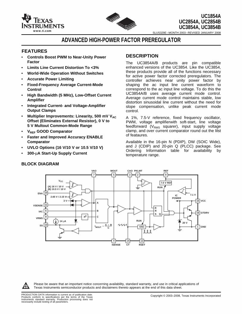
BLOCK DIAGRAM
10
11
6
8
15
1
16
ENA
VSENSE
IAC
VRMS
VCC
GND
GTDRV
2.65 V / 2.15 V
3 V
7
VAO
13SS
X2
A
B
C
(A) 16 V / 10 V(B) 10.5 V / 10 V
5
MOUT
4
ISENSE
3
CAO
14
CT
OSC
12
RSET
S Q
RR
2
PKLMT
20 V
ICPOWER
7.5 V REF
9
REF
RUN
7.1 V
RUN
VCC
14 µA
IMOUTA B
C
UC1854AUC2854A, UC2854BUC3854A, UC3854B
SLUS329E–MONTH 2003–REVISED JANUARY 2008www.ti.com
ADVANCED HIGH-POWER FACTOR PREREGULATOR
• Controls Boost PWM to Near-Unity PowerFactor The UC3854A/B products are pin compatible
enhanced versions of the UC3854. Like the UC3854,• Limits Line Current Distortion To <3%these products provide all of the functions necessary• World-Wide Operation Without Switchesfor active power factor corrected preregulators. The
• Accurate Power Limiting controller achieves near unity power factor by• Fixed-Frequency Average Current-Mode shaping the ac input line current waveform to
correspond to the ac input line voltage. To do this theControlUC3854A/B uses average current mode control.• High Bandwidth (5 MHz), Low-Offset Current Average current mode control maintains stable, lowAmplifier distortion sinusoidal line current without the need for
• Integrated Current- and Voltage-Amplifier slope compensation, unlike peak current modeOutput Clamps control.
• Multiplier Improvements: Linearity, 500 mV VAC A 1%, 7.5-V reference, fixed frequency oscillator,Offset (Eliminates External Resistor), 0 V to PWM, voltage amplifierwith soft-start, line voltage5 V Multout Common-Mode Range feedforward (VRMS squarer), input supply voltage
clamp, and over current comparator round out the lilst• VREF GOOD Comparatorof feataures.• Faster and Improved Accuracy ENABLE
Comparator Available in the 16-pin N (PDIP), DW (SOIC Wide),and J (CDIP) and 20-pin Q (PLCC) package. See• UVLO Options (16 V/10 V or 10.5 V/10 V)Ordering Information table for availability by
• 300-µA Start-Up Supply Current temperature range.
1
Please be aware that an important notice concerning availability, standard warranty, and use in critical applications ofTexas Instruments semiconductor products and disclaimers thereto appears at the end of this data sheet.
PRODUCTION DATA information is current as of publication date. Copyright © 2003–2008, Texas Instruments IncorporatedProducts conform to specifications per the terms of the TexasInstruments standard warranty. Production processing does notnecessarily include testing of all parameters.
www.ti.com
DESCRIPTION (CONTINUED)
ABSOLUTE MAXIMUM RATINGS
UC1854AUC2854A, UC2854BUC3854A, UC3854BSLUS329E–MONTH 2003–REVISED JANUARY 2008
These devices have limited built-in ESD protection. The leads should be shorted together or the device placed in conductive foamduring storage or handling to prevent electrostatic damage to the MOS gates.
The UC3854A/B products improve upon the UC3854 by offering a wide bandwidth, low offset current amplifier, afaster responding and improved accuracy enable comparator, a VREF GOOD comparator, UVLO thresholdoptions (16 V/10 V for offline, 10.5 V/10 V for startup from an auxiliary 12-V regulator), lower startup supplycurrent, and an enhanced multiply/divide circuit. New features like the amplifier output clamps, improved amplifiercurrent sinking capability, and low offset VAC pin reduce the external component count while improvingperformance. Improved common mode input range of the multiplier output/current amplifier input allow thedesigner greater flexibility in choosing amethod for current sensing. Unlike its predecessor, RSET controls onlyoscillator charging current and has no effect on clamping the maximum multiplier output current. This current isnow clamped to a maximum of 2 × IAC at all times which simplifies the design process and provides foldbackpower limiting during brownout and extreme low line conditions.
ORDERING INFORMATIONUVLO UVLO PART NUMBERS
TURN-ON TURN-OFFTA CDIP-16 PDIP-16 SOIC-16 PLCC-20(V) (V) (V) (N) (DW) (Q)16 10 – – – –
–55°C to 125°C10.5 10 UC1854BJ – – –16 10 UC2854AJ UC2854AN UC2854ADW UC2854AQ
–40°C to 85°C10.5 10 UC2854BJ UC2854BN UC2854BDW UC2854BQ16 10 – UC2854AN UC2854ADW –
0°C to 70°C10.5 10 – UC2854BN UC2854BDW –
over operating free-air temperature range (unless otherwise noted) (1)
UCX854A, UCX854B UNITVCC Supply voltage 22 V
Continuous 0.5IGTDRV GTDRV current A
50% duty cycle 1.5VSENSE, VRMS, ISENSE MOUT 11
Input voltage VPKLMT 5
Input current RSET, IAC, PKLMT, ENA 10 mAPower dissipation 1 W
TJ Junction temperature –55 to 150Tstg Storage temperature –65 to 150 °CTsol Lead temperataure, 1,6 mm (1/16 inch) from case for 10 seconds 300
(1) Stresses beyond those listed under absolutemaximum ratings may cause permanent damage to the device. These are stress ratingsonly, and functional operation of the device at these or any other conditions beyond those indicated under recommended operatingconditions is not implied. Exposure to absolute-maximum-rated conditions for extended periodsmayaffect device reliability. All voltagesarewith respect to GND. Currents are positive into and negative out of, the specified terminal. ENA input is internally clamped toapproximately 10 V.
2 Submit Documentation Feedback Copyright © 2003–2008, Texas Instruments Incorporated
Product Folder Link(s): UC1854A UC2854A, UC2854B UC3854A, UC3854B
www.ti.com
RECOMMENDED OPERATING CONDITIONS
THERMAL RESISTANCE
UC1854AUC2854A, UC2854BUC3854A, UC3854B
SLUS329E–MONTH 2003–REVISED JANUARY 2008
over operating free-air temperature range (unless otherwise noted)
MIN MAX UNITVCC Supply voltage 10 20 V
UC1854X –55 125TJ Operating junction temperature UC2854X –40 85 °C
UC3854X 0 70
PACKAGED DEVICESRESISTANCES CDIP-16 PDIP-16 SOP-16 PLCC-20
(J) (N) (DW) (Q)θJC (°C/W) 28 (1) 45 27 34θJA (°C/W) 80–120 90 (2) 50–130 (2) 43–75 (2)
(1) θJC data values stated are derived from MIL-STD-1835B which states gthe baseline values shown are worst case (mean +2s) for a 60 ×60 mil microcircuit device silicon die and applicable for devices with die sizes up to 14,400 square mils. For device die sizes greater than14,400 square mils use the following values, dual-in-line, 11°C/W; flat pack and pin grid array, 10°C/W.are at the end of each trace.
(2) θJA (junction-to-ambient) applies to devices mounted to five square inch FR4 PC board with one ounce copper where noted. Whenresitance range is given, lower values are for five square inch aluminum PC board. Test PWB is 0.062 inches thick and typically uses0,635 mm trace widths for power packages and 1,3 mm trace widths for non-power packages with a 100 × 100 mil probe land are at theend of each trace.
Copyright © 2003–2008, Texas Instruments Incorporated Submit Documentation Feedback 3
Product Folder Link(s): UC1854A UC2854A, UC2854B UC3854A, UC3854B
www.ti.com
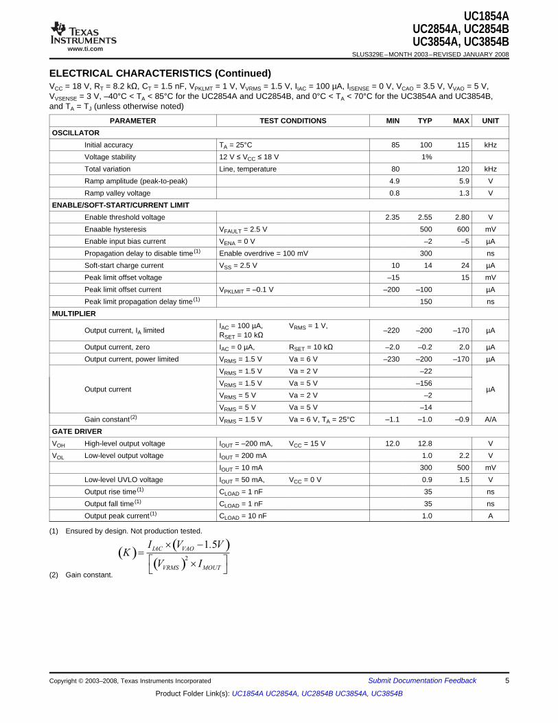
ELECTRICAL CHARACTERISTICS
UC1854AUC2854A, UC2854BUC3854A, UC3854BSLUS329E–MONTH 2003–REVISED JANUARY 2008
VCC = 18 V, RT = 8.2 kΩ, CT = 1.5 nF, VPKLMT = 1 V, VVRMS = 1.5 V, IIAC = 100 µA, IISENSE = 0 V, VCAO = 3.5 V, VVAO = 5 V,VVSENSE = 3 V, –40°C < TA < 85°C for the UC2854A and UC2854B, and 0°C < TA < 70°C for the UC3854A and UC3854B,and TA = TJ (unless otherwise noted)
PARAMETER TEST CONDITIONS MIN TYP MAX UNITOVERALL
CAO = 0 V, VAO = 0 V,Supply current, off 250 400 µAVCC = VUVLO–0.3 VSupply current, on 12 18 mA
UCx854A 15.0 16.0 17.5VCC turn-on threshold voltage
UCx854B 8.0 10.5 11.2UCx854A 9 10 12
VCC turn-off threshold voltageUCx854B 7.8 10.3 11.0 VUCx854A 5 6 7
VCC hysteresisUCx854B 0.10 0.22 0.50
VCC clamp IVCC = IVCC(on) + 5 mA 18 20 22VOLTAGE AMPLIFIER
Input voltage 2.9 3.0 3.1 VVSENSE bias current –500 —25 500 nAOpen loop gain 2 V ≤ VOUT ≤ 5 V 70 100 dB
VOH High-level output voltage ILOAD = –500 µA 6V
VOL Low-level output voltage ILOAD = 500 µA 0.3 0.5ISC Output short-circuit current VOUT = 0 V 1.5 3.5 mA
Gain bandwidth product (1) fIN = 100 kHz, 10 mVp-p 1 MHzCURRENT AMPLIFIER
VCM = 0 V, TA = 25°C –4 0Input offset voltage mV
VCM = 0 V, Overtemperature –5.5 0ISENSE Input bias current VCM = 0 V –500 500 nA
Open loop gain 2 V ≤ VOUT = 6 V 80 110 dBVOH High-level output voltage ILOAD = –500 µA 8
VVOL Low-level output voltage ILOAD = 500 µA 0.3 0.5ISC Output short-circuit current VOUT = 0 V 1.5 3.5 mACMRR Common mode rejection range –0.3 5.0 V
Gain bandwidth product (1) fIN = 100 kHz, 10 mVp-p 3 5 MHzREFERENCE
IREF = 0 mA, TA = 25°C 7.4 7.5 7.6Output voltage V
IREF = 0 mA 7.35 7.50 7.65Load regulation 1 mA ≤ IREF ≤ 10 mA 0 8 20
mVLine regulation 12 V ≤ VCC ≤ 18 V 0 14 25
ISC Short circuit current VREF = 0 V 25 35 60 mA
(1) Ensured by design. Not production tested.
4 Submit Documentation Feedback Copyright © 2003–2008, Texas Instruments Incorporated
Product Folder Link(s): UC1854A UC2854A, UC2854B UC3854A, UC3854B
www.ti.com
ELECTRICAL CHARACTERISTICS (Continued)
(2) Gain constant.
( ) ( )( )2
1 5IAC VAO
VRMS MOUT
I V . VK
V I
´ -=
é ù´ë û
UC1854AUC2854A, UC2854BUC3854A, UC3854B
SLUS329E–MONTH 2003–REVISED JANUARY 2008
VCC = 18 V, RT = 8.2 kΩ, CT = 1.5 nF, VPKLMT = 1 V, VVRMS = 1.5 V, IIAC = 100 µA, IISENSE = 0 V, VCAO = 3.5 V, VVAO = 5 V,VVSENSE = 3 V, –40°C < TA < 85°C for the UC2854A and UC2854B, and 0°C < TA < 70°C for the UC3854A and UC3854B,and TA = TJ (unless otherwise noted)
PARAMETER TEST CONDITIONS MIN TYP MAX UNITOSCILLATOR
Initial accuracy TA = 25°C 85 100 115 kHzVoltage stability 12 V ≤ VCC ≤ 18 V 1%Total variation Line, temperature 80 120 kHzRamp amplitude (peak-to-peak) 4.9 5.9 VRamp valley voltage 0.8 1.3 V
ENABLE/SOFT-START/CURRENT LIMITEnable threshold voltage 2.35 2.55 2.80 VEnaable hysteresis VFAULT = 2.5 V 500 600 mVEnable input bias current VENA = 0 V –2 –5 µAPropagation delay to disable time (1) Enable overdrive = 100 mV 300 nsSoft-start charge current VSS = 2.5 V 10 14 24 µAPeak limit offset voltage –15 15 mVPeak limit offset current VPKLMIT = –0.1 V –200 –100 µAPeak limit propagation delay time (1) 150 ns
MULTIPLIERIAC = 100 µA, VRMS = 1 V,Output current, IA limited –220 –200 –170 µARSET = 10 kΩ
Output current, zero IAC = 0 µA, RSET = 10 kΩ –2.0 –0.2 2.0 µAOutput current, power limited VRMS = 1.5 V Va = 6 V –230 –200 –170 µA
VRMS = 1.5 V Va = 2 V –22VRMS = 1.5 V Va = 5 V –156
Output current µAVRMS = 5 V Va = 2 V –2VRMS = 5 V Va = 5 V –14
Gain constant (2) VRMS = 1.5 V Va = 6 V, TA = 25°C –1.1 –1.0 –0.9 A/AGATE DRIVERVOH High-level output voltage IOUT = –200 mA, VCC = 15 V 12.0 12.8 VVOL Low-level output voltage IOUT = 200 mA 1.0 2.2 V
IOUT = 10 mA 300 500 mVLow-level UVLO voltage IOUT = 50 mA, VCC = 0 V 0.9 1.5 VOutput rise time (1) CLOAD = 1 nF 35 nsOutput fall time (1) CLOAD = 1 nF 35 nsOutput peak current (1) CLOAD = 10 nF 1.0 A
(1) Ensured by design. Not production tested.
Copyright © 2003–2008, Texas Instruments Incorporated Submit Documentation Feedback 5
Product Folder Link(s): UC1854A UC2854A, UC2854B UC3854A, UC3854B

www.ti.com
PACKAGE DESCRIPTION
1
2
3
4
5
6
7
8
16
15
14
13
12
11
10
9
GNDPKLMT
CAOISENSE
MOUTIAC
VAOVRMS
GTDRVVCCCTSSRSETVSENSEENAVREF
J, N and DW PACKAGES(TOP VIEW)
5
4
6
7
8
18
17
16
15
14
ISENSECAOUT
N/CMOUT
IAC
CTSSN/CRSETVSENSE
3 2 1 20 19
9 10 11 12 13
PK
LMT
GN
DN
/CG
TD
RV
VC
C
VA
OV
RM
SN
CV
RE
FE
NA
Q PACKAGE(TOP VIEW)
N/C − No connection
UC1854AUC2854A, UC2854BUC3854A, UC3854BSLUS329E–MONTH 2003–REVISED JANUARY 2008
6 Submit Documentation Feedback Copyright © 2003–2008, Texas Instruments Incorporated
Product Folder Link(s): UC1854A UC2854A, UC2854B UC3854A, UC3854B
www.ti.com
UC1854AUC2854A, UC2854BUC3854A, UC3854B
SLUS329E–MONTH 2003–REVISED JANUARY 2008
TERMINAL FUNCTIONSTERMINAL
PACKAGES I/O DESCRIPTIONNAME
J/N/DW Q/LOutput of the wide bandwidth current amplifier and one of the inputs to the PWM duty-cycle
CAO 3 4 O comparator. The output signal generated by this amplifier commands the PWM to force the correctinput current. The output can swing from 0.1 V to 7.5 V.
CT 14 18 I Capacitor from CT to GND sets the PWM oscillator frequency.A nominal voltage above 2.65 V on this pin allows the device to begin operating. Once operating,ENA 10 13 I the device shuts off if this pin goes below 2.15 V nominal.All bypass and timing capacitors connected to GND should have leads as short and direct asGND 1 2 – possible. All voltages are measured with respect GND.Output of the PWM is a 1.5-A peak totem-pole MOSFET gate driver on GTDRV. Use a series gateresistor of at least 5 Ω to prevent interaction between the gate impedance and the GTDRV outputGTDRV 16 20 O driver that might cause the GTDRV output to overshoot excessively. Some overshoot of theGTDRV output is always expected when driving a capacitive load.Current input to the multiplier, proportional to the instantaneous line voltage. This input to theanalog multiplier is a current. The multiplier is tailored for very low distortion from this current inputIAC 6 8 I (IAC) to MOUT, so this is the only multiplier input that should be used for sensing instantaneousline voltage.Switch current sensing input. This is the inverting input to the current amplifier. This input and the
ISENSE 4 5 I non-inverting input MOUT remain functional down to and below GND. Care should be taken toavoid taking these inputs below –0.5 V, because they are protected with diodes to GND.Multiplier output and current sense plus. The output of the analog multiplier and the non-invertinginput of the current amplifier are connected together at MOUT. The cautions about taking ISENSE
MOUT 5 7 I/O below –0.5 V also apply to MOUT. As the multiplier output is a current, this is a high-impedanceinput similar to ISENSE, so the current amplifier can be configured as a differential amplifier to rejectGND noise. IMOUT ≤ 2 × IAC
Peak limit. The threshold for PKLMT is 0.0 V. Connect this input to the negative voltage on thePKLMT 2 3 I current sense resistor. Use a resistor to REF to offset the negative current sense signal up to GND.Oscillator charging current and multiplier limit set. A resistor from RSET to ground programsRSET 12 15 I oscillator charging current.Soft-start. SS remains at GND as long as the device is disabled or VCC is too low. SS pulls up toover 3 V by an internal 14-µA current source when both VCC becomes valid and the device isenabled. SS acts as the reference input to the voltage amplifier if SS is below VREF. With a largeSS 13 17 I capacitor from SS to GND, the reference to the voltage regulating amplifier rises slowly, andincrease the PWM duty cycle slowly. In the event of a disable command or a supply dropout, SSwill quickly discharge to ground and disable the PWM.
VAO 7 9 I Voltage amplifier outputVCC 15 19 I Positive supply rail
Used to set the peak limit point and as an internal reference for various device functions. ThisVREF 9 12 O voltage must be present for the device to operate.One of the inputs into the multiplier. This pin provides the input RMS voltage to the multiplierVRMS 8 10 I circuitry.This pin provides the feedback from the output. This input goes into the voltage error amplifier andVSENSE 11 14 I the output of the error amplifier is another of the inputs into the multiplier circuit.
Copyright © 2003–2008, Texas Instruments Incorporated Submit Documentation Feedback 7
Product Folder Link(s): UC1854A UC2854A, UC2854B UC3854A, UC3854B
www.ti.com
FUNCTIONAL DESCRIPTION
Multiply/Square and Divide
The UC3854A/B multiplier design maintains the same gain constant
1K
V
-æ ö=ç ÷è ø as the UC3854. The
( )( )2
1 5VAO
MOUT IAC
VRMS
V . VI I
K V
-= ´
´(1)
270 1 4141 53
250IAC
.R . M
Am´
= = W(2)
UC1854AUC2854A, UC2854BUC3854A, UC3854BSLUS329E–MONTH 2003–REVISED JANUARY 2008
The UC3854A and UC3854B family of products are designed as pin compatible upgrades to the industrystandard UC3854 active power factor correction circuits. The circuit enhancements allow the user to eliminate inmost cases several external components currently required to successfully apply the UC3854. In addition,linearity improvements to the multiply, square and divide circuitry optimizes overall system performance. Detaileddescriptions of the circuit enhancements are provided below. For in-depth design applications reference datarefer to the application notes, UC3854 Controlled Power Factor Correction Circuit Design (SLUA144) andUC3854A and UC3854B Advanced Power Factor Correction Control ICs (SLUA177).
relationship between the inputs and output current is given as:
This is nearly the same as the UC3854, but circuit differences have improved the performance and application.
The first difference is with the IAC input. The UC3854A/B regulated this pin voltage to the nominal 500 mV overthe full operating temperature range, rather than the 6.0 V used on the UC3854. The low offset voltageeliminates the need for a line zero crossing compensating resistor to VREF from IAC that UC3854 designsrequire. The maximum current at high line into IAC should be limited to 250 µA for best performance.
Therefore, if VVAC(max) = 270 V,
The VRMS pin linear operating range is improved with the UC3854A/B as well. The input range for VRMS extendsfrom 0 V to 5.5 V. Since the UC3854A squaring circuit employs an analog multiplier, rather than a linearapproximation, accuracy is improved, and discontinuities are eliminated. The external divider network connectedto VRMS should produce 1.5 V at low line (85 VAC). This puts 4.77 V on VRMS at high line (270 VAC) which iswell within its operating range.
The voltage amplifier output forms the third input to the multiplier and is internally clamped to 6.0 V. Thiseliminated an external zener clamp often used in UC3854 designs. The offset voltage at this input to themultiplier has been raised on the UC3854A/B to 1.5 V.
The multiplier output pin, which is also common to the current amplifier non-inverting input, has a –0.3 V to 5.0 Voutput range, compared to the –0.3 V to 2.5 V range of the UC3854. This improvement allows the UC3854A/B tobe used in applications where the current sense signal amplitude is very large.
8 Submit Documentation Feedback Copyright © 2003–2008, Texas Instruments Incorporated
Product Folder Link(s): UC1854A UC2854A, UC2854B UC3854A, UC3854B
www.ti.com
Voltage Amplifier
Current Amplifier
Miscellaneous
UC1854AUC2854A, UC2854BUC3854A, UC3854B
SLUS329E–MONTH 2003–REVISED JANUARY 2008
The UC3854A/B voltage amplifier design is essentially similar to the UC3854 with two exceptions. The first iswith the internal connection. The lower voltage reduces the amount of charge on the compensation capacitors,which provides improved recovery form large signal events, such as line dropouts, or power interruption. It alsominimizes the dc current flowing through the feedback. The output of the voltage amplifier is also changed. Inaddition to a 6.0-V temperature compensated clamp, the output short circuit current has been lowered to 2 mAtypical, and an active pull down has replaced the passive pull down of the UC3854.
The current amplifier for an average current PFC controller needs a low offset voltage in order to minimize ac linecurrent distortion. With this in mind, the UC3854A/B current amplifier has improved the input offset voltage from±4 mV to 0 V to ±3 mV. The negative offset of the UC3854A/B assures that the PWM circuit will not drive theMOSFET is the current command is zero (both current amplifier inputs zero.) Previous designs required anexternal offset cancellation network to implement this key feature. The bandwidth of the current amplifier hasbeen improved as well to 5 MHz typical. While this is not generally an issue at 50 Hz or 60 Hz inputs, it isessential for 400 Hz input avionics applications.
Several other important enhancements have been implemented in the UC3854A/B. AVCC supply voltage clamp at20 V allows the controller to be current fed if desired. The lower startup supply current (250 µA typical),substantially reduces the power requirements of an offline startup resistor. The 10.5 V/10 V UVLO option(UC3854B) enables the controller to be powered off of an auxiliary 12-V supply.
The VREF GOOD comparator assures that the MOSFET driver output remains low if the supply of the 7.5 Vreference are not yet up. This improvement eliminates the need for external Schottky diodes on the PKLMT andMult Out pins that some UC3854 designs require. The propagation delay of the disable feature has beenimproved to 300 ns typical. This delay was proportional to the size of the VREF capacitor on the UC3854, and istypically several orders of magnitude slower.
Copyright © 2003–2008, Texas Instruments Incorporated Submit Documentation Feedback 9
Product Folder Link(s): UC1854A UC2854A, UC2854B UC3854A, UC3854B
www.ti.com
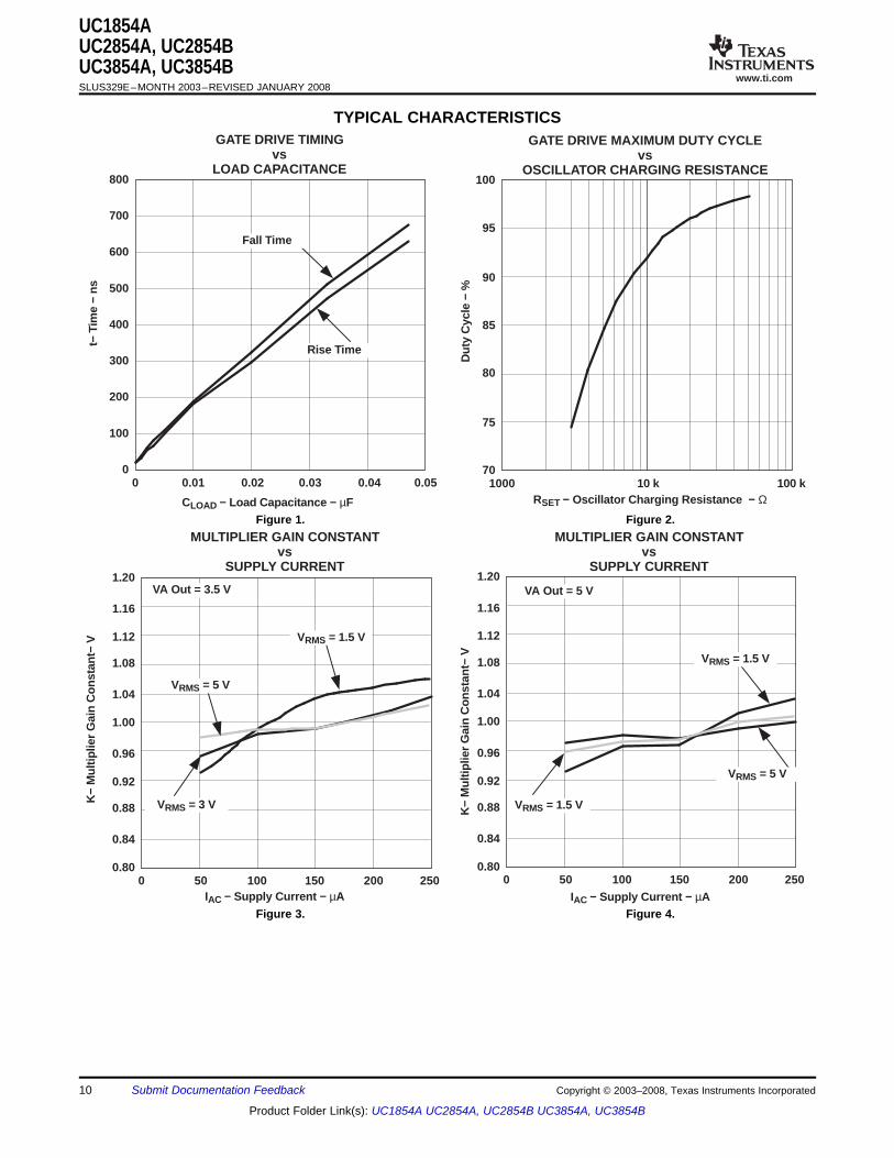
TYPICAL CHARACTERISTICS
100070
75
80
85
90
95
100
10 k 100 k
GATE DRIVE MAXIMUM DUTY CYCLEvs
OSCILLAT OR CHARGING RESISTANCE
RSET − Oscillator Charging Resistance − Ω
Dut
y C
ycle
− %
00
100
300
400
500
600
800
200
700
0.01 0.02 0.03 0.04 0.05
GATE DRIVE TIMINGvs
LOAD CAPACITANCE
CLOAD − Load Capacitance − µF
t− T
ime
− ns
Rise Time
Fall Time
0
0.84
0.8050 100
0.88
0.96
0.92
1.00
1.04
1.08
1.16
1.12
1.20
150 200 250
MULTIPLIER GAIN CONSTANTvs
SUPPLY CURRENT
IAC − Supply Current − µA
K−
Mul
tiplie
r Gai
n C
onst
ant−
V
VRMS = 3 V
VRMS = 5 V
VRMS = 1.5 V
VA Out = 3.5 V
MULTIPLIER GAIN CONSTANTvs
SUPPLY CURRENT
IAC − Supply Current − µA0
0.84
0.8050 100
0.88
0.96
0.92
1.00
1.04
1.08
1.16
1.12
1.20
150 200 250
VRMS = 1.5 V
VRMS = 1.5 V
VRMS = 5 V
K−
Mul
tiplie
r Gai
n C
onst
ant−
V
VA Out = 5 V
UC1854AUC2854A, UC2854BUC3854A, UC3854BSLUS329E–MONTH 2003–REVISED JANUARY 2008
Figure 1. Figure 2.
Figure 3. Figure 4.
10 Submit Documentation Feedback Copyright © 2003–2008, Texas Instruments Incorporated
Product Folder Link(s): UC1854A UC2854A, UC2854B UC3854A, UC3854B
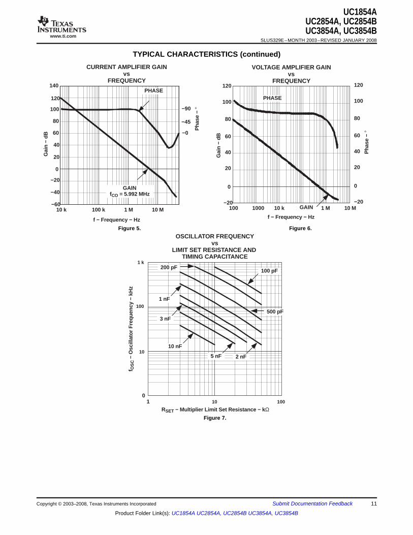
www.ti.com
0
−20
40
20
60
80
100
120
100 1000 10 k 100 k 1 M 10 M
VOLTAGE AMPLIFIER GAINvs
FREQUENCY
GAIN
PHASE
f − Frequency − HzG
ain
− dB
0
−20
40
20
60
80
100
120
Pha
se −
°
10 k−60
100 k
−40
0
20
60
80
100
120
1 M 10 M
−20
40
140
CURRENT AMPLIFIER GAINvs
FREQUENCY
GAINfCO = 5.992 MHz
f − Frequency − Hz
Gai
n −
dB
PHASE
−90
−45
−0
Pha
se −
°
OSCILLAT OR FREQUENCYvs
LIMIT SET RESISTANCE AND TIMING CAPACITANCE
RSET − Multiplier Limit Set Resistance − k Ω
f OS
C −
Osc
illat
or F
requ
ency
− k
Hz
10
10 100
10
100
1 k
10 nF
5 nF 2 nF
3 nF
1 nF
500 pF
200 pF100 pF
UC1854AUC2854A, UC2854BUC3854A, UC3854B
SLUS329E–MONTH 2003–REVISED JANUARY 2008
TYPICAL CHARACTERISTICS (continued)
Figure 5. Figure 6.
Figure 7.
Copyright © 2003–2008, Texas Instruments Incorporated Submit Documentation Feedback 11
Product Folder Link(s): UC1854A UC2854A, UC2854B UC3854A, UC3854B

PACKAGE OPTION ADDENDUM
www.ti.com 29-Jul-2017
Addendum-Page 1
PACKAGING INFORMATION
Orderable Device Status(1)
Package Type PackageDrawing
Pins PackageQty
Eco Plan(2)
Lead/Ball Finish(6)
MSL Peak Temp(3)
Op Temp (°C) Device Marking(4/5)
Samples
5962-9326102MEA ACTIVE CDIP J 16 1 TBD A42 N / A for Pkg Type -55 to 125 5962-9326102MEAUC1854BJ/883B
UC1854BJ ACTIVE CDIP J 16 1 TBD A42 N / A for Pkg Type -55 to 125 UC1854BJ
UC1854BJ883B ACTIVE CDIP J 16 1 TBD A42 N / A for Pkg Type -55 to 125 5962-9326102MEAUC1854BJ/883B
UC2854ADW ACTIVE SOIC DW 16 40 Green (RoHS& no Sb/Br)
CU NIPDAU Level-2-260C-1 YEAR -40 to 85 UC2854ADW
UC2854ADWG4 ACTIVE SOIC DW 16 40 Green (RoHS& no Sb/Br)
CU NIPDAU Level-2-260C-1 YEAR -40 to 85 UC2854ADW
UC2854ADWTR ACTIVE SOIC DW 16 2000 Green (RoHS& no Sb/Br)
CU NIPDAU Level-2-260C-1 YEAR -40 to 85 UC2854ADW
UC2854AN ACTIVE PDIP N 16 25 Green (RoHS& no Sb/Br)
CU NIPDAU N / A for Pkg Type -40 to 85 UC2854AN
UC2854ANG4 ACTIVE PDIP N 16 25 Green (RoHS& no Sb/Br)
CU NIPDAU N / A for Pkg Type -40 to 85 UC2854AN
UC2854BDW ACTIVE SOIC DW 16 40 Green (RoHS& no Sb/Br)
CU NIPDAU Level-2-260C-1 YEAR -40 to 85 UC2854BDW
UC2854BDWG4 ACTIVE SOIC DW 16 40 Green (RoHS& no Sb/Br)
CU NIPDAU Level-2-260C-1 YEAR -40 to 85 UC2854BDW
UC2854BDWTR ACTIVE SOIC DW 16 2000 Green (RoHS& no Sb/Br)
CU NIPDAU Level-2-260C-1 YEAR -40 to 85 UC2854BDW
UC2854BDWTRG4 ACTIVE SOIC DW 16 2000 Green (RoHS& no Sb/Br)
CU NIPDAU Level-2-260C-1 YEAR -40 to 85 UC2854BDW
UC2854BN ACTIVE PDIP N 16 25 Green (RoHS& no Sb/Br)
CU NIPDAU N / A for Pkg Type -40 to 85 UC2854BN
UC2854BNG4 ACTIVE PDIP N 16 25 Green (RoHS& no Sb/Br)
CU NIPDAU N / A for Pkg Type -40 to 85 UC2854BN
UC2854BQ NRND PLCC FN 20 46 Green (RoHS& no Sb/Br)
CU SN Level-2-260C-1 YEAR -40 to 85 UC2854BQ
UC2854J ACTIVE CDIP J 16 1 TBD A42 N / A for Pkg Type -40 to 85 UC2854J
PACKAGE OPTION ADDENDUM
www.ti.com 29-Jul-2017
Addendum-Page 2
Orderable Device Status(1)
Package Type PackageDrawing
Pins PackageQty
Eco Plan(2)
Lead/Ball Finish(6)
MSL Peak Temp(3)
Op Temp (°C) Device Marking(4/5)
Samples
UC3854ADW ACTIVE SOIC DW 16 40 Green (RoHS& no Sb/Br)
CU NIPDAU Level-2-260C-1 YEAR 0 to 70 UC3854ADW
UC3854ADWG4 ACTIVE SOIC DW 16 40 Green (RoHS& no Sb/Br)
CU NIPDAU Level-2-260C-1 YEAR 0 to 70 UC3854ADW
UC3854ADWTR ACTIVE SOIC DW 16 2000 Green (RoHS& no Sb/Br)
CU NIPDAU Level-2-260C-1 YEAR 0 to 70 UC3854ADW
UC3854ADWTRG4 ACTIVE SOIC DW 16 2000 Green (RoHS& no Sb/Br)
CU NIPDAU Level-2-260C-1 YEAR 0 to 70 UC3854ADW
UC3854AN ACTIVE PDIP N 16 25 Green (RoHS& no Sb/Br)
CU NIPDAU N / A for Pkg Type 0 to 70 UC3854AN
UC3854ANG4 ACTIVE PDIP N 16 25 Green (RoHS& no Sb/Br)
CU NIPDAU N / A for Pkg Type 0 to 70 UC3854AN
UC3854BDW ACTIVE SOIC DW 16 40 Green (RoHS& no Sb/Br)
CU NIPDAU Level-2-260C-1 YEAR 0 to 70 UC3854BDW
UC3854BDWG4 ACTIVE SOIC DW 16 40 Green (RoHS& no Sb/Br)
CU NIPDAU Level-2-260C-1 YEAR 0 to 70 UC3854BDW
UC3854BDWTR ACTIVE SOIC DW 16 2000 Green (RoHS& no Sb/Br)
CU NIPDAU Level-2-260C-1 YEAR 0 to 70 UC3854BDW
UC3854BDWTRG4 ACTIVE SOIC DW 16 2000 Green (RoHS& no Sb/Br)
CU NIPDAU Level-2-260C-1 YEAR 0 to 70 UC3854BDW
UC3854BN ACTIVE PDIP N 16 25 Green (RoHS& no Sb/Br)
CU NIPDAU N / A for Pkg Type 0 to 70 UC3854BN
UC3854BNG4 ACTIVE PDIP N 16 25 Green (RoHS& no Sb/Br)
CU NIPDAU N / A for Pkg Type 0 to 70 UC3854BN
(1) The marketing status values are defined as follows:ACTIVE: Product device recommended for new designs.LIFEBUY: TI has announced that the device will be discontinued, and a lifetime-buy period is in effect.NRND: Not recommended for new designs. Device is in production to support existing customers, but TI does not recommend using this part in a new design.PREVIEW: Device has been announced but is not in production. Samples may or may not be available.OBSOLETE: TI has discontinued the production of the device.
(2) RoHS: TI defines "RoHS" to mean semiconductor products that are compliant with the current EU RoHS requirements for all 10 RoHS substances, including the requirement that RoHS substancedo not exceed 0.1% by weight in homogeneous materials. Where designed to be soldered at high temperatures, "RoHS" products are suitable for use in specified lead-free processes. TI mayreference these types of products as "Pb-Free".RoHS Exempt: TI defines "RoHS Exempt" to mean products that contain lead but are compliant with EU RoHS pursuant to a specific EU RoHS exemption.Green: TI defines "Green" to mean the content of Chlorine (Cl) and Bromine (Br) based flame retardants meet JS709B low halogen requirements of <=1000ppm threshold. Antimony trioxide basedflame retardants must also meet the <=1000ppm threshold requirement.
PACKAGE OPTION ADDENDUM
www.ti.com 29-Jul-2017
Addendum-Page 3
(3) MSL, Peak Temp. - The Moisture Sensitivity Level rating according to the JEDEC industry standard classifications, and peak solder temperature.
(4) There may be additional marking, which relates to the logo, the lot trace code information, or the environmental category on the device.
(5) Multiple Device Markings will be inside parentheses. Only one Device Marking contained in parentheses and separated by a "~" will appear on a device. If a line is indented then it is a continuationof the previous line and the two combined represent the entire Device Marking for that device.
(6) Lead/Ball Finish - Orderable Devices may have multiple material finish options. Finish options are separated by a vertical ruled line. Lead/Ball Finish values may wrap to two lines if the finishvalue exceeds the maximum column width.
Important Information and Disclaimer:The information provided on this page represents TI's knowledge and belief as of the date that it is provided. TI bases its knowledge and belief on informationprovided by third parties, and makes no representation or warranty as to the accuracy of such information. Efforts are underway to better integrate information from third parties. TI has taken andcontinues to take reasonable steps to provide representative and accurate information but may not have conducted destructive testing or chemical analysis on incoming materials and chemicals.TI and TI suppliers consider certain information to be proprietary, and thus CAS numbers and other limited information may not be available for release.
In no event shall TI's liability arising out of such information exceed the total purchase price of the TI part(s) at issue in this document sold by TI to Customer on an annual basis.
OTHER QUALIFIED VERSIONS OF UC1854B, UC2854B, UC2854M, UC3854B :
• Catalog: UC3854B, UC2854
• Enhanced Product: UC2854B-EP
• Military: UC2854BM, UC1854B
NOTE: Qualified Version Definitions:
• Catalog - TI's standard catalog product
• Enhanced Product - Supports Defense, Aerospace and Medical Applications
• Military - QML certified for Military and Defense Applications
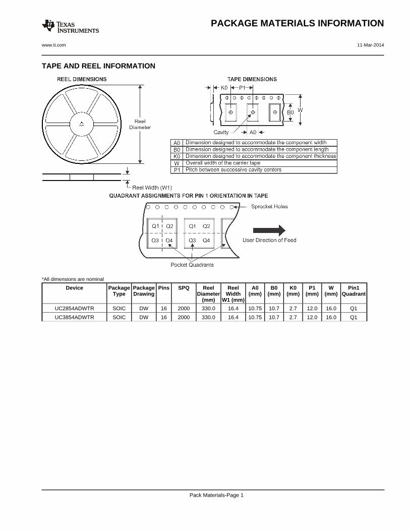
TAPE AND REEL INFORMATION
*All dimensions are nominal
Device PackageType
PackageDrawing
Pins SPQ ReelDiameter
(mm)
ReelWidth
W1 (mm)
A0(mm)
B0(mm)
K0(mm)
P1(mm)
W(mm)
Pin1Quadrant
UC2854ADWTR SOIC DW 16 2000 330.0 16.4 10.75 10.7 2.7 12.0 16.0 Q1
UC3854ADWTR SOIC DW 16 2000 330.0 16.4 10.75 10.7 2.7 12.0 16.0 Q1
PACKAGE MATERIALS INFORMATION
www.ti.com 11-Mar-2014
Pack Materials-Page 1
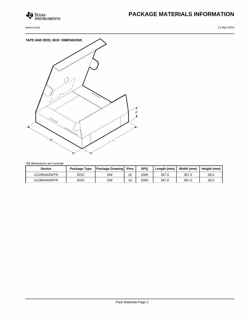
*All dimensions are nominal
Device Package Type Package Drawing Pins SPQ Length (mm) Width (mm) Height (mm)
UC2854ADWTR SOIC DW 16 2000 367.0 367.0 38.0
UC3854ADWTR SOIC DW 16 2000 367.0 367.0 38.0
PACKAGE MATERIALS INFORMATION
www.ti.com 11-Mar-2014
Pack Materials-Page 2
IMPORTANT NOTICE
Texas Instruments Incorporated (TI) reserves the right to make corrections, enhancements, improvements and other changes to itssemiconductor products and services per JESD46, latest issue, and to discontinue any product or service per JESD48, latest issue. Buyersshould obtain the latest relevant information before placing orders and should verify that such information is current and complete.TI’s published terms of sale for semiconductor products (http://www.ti.com/sc/docs/stdterms.htm) apply to the sale of packaged integratedcircuit products that TI has qualified and released to market. Additional terms may apply to the use or sale of other types of TI products andservices.Reproduction of significant portions of TI information in TI data sheets is permissible only if reproduction is without alteration and isaccompanied by all associated warranties, conditions, limitations, and notices. TI is not responsible or liable for such reproduceddocumentation. Information of third parties may be subject to additional restrictions. Resale of TI products or services with statementsdifferent from or beyond the parameters stated by TI for that product or service voids all express and any implied warranties for theassociated TI product or service and is an unfair and deceptive business practice. TI is not responsible or liable for any such statements.Buyers and others who are developing systems that incorporate TI products (collectively, “Designers”) understand and agree that Designersremain responsible for using their independent analysis, evaluation and judgment in designing their applications and that Designers havefull and exclusive responsibility to assure the safety of Designers' applications and compliance of their applications (and of all TI productsused in or for Designers’ applications) with all applicable regulations, laws and other applicable requirements. Designer represents that, withrespect to their applications, Designer has all the necessary expertise to create and implement safeguards that (1) anticipate dangerousconsequences of failures, (2) monitor failures and their consequences, and (3) lessen the likelihood of failures that might cause harm andtake appropriate actions. Designer agrees that prior to using or distributing any applications that include TI products, Designer willthoroughly test such applications and the functionality of such TI products as used in such applications.TI’s provision of technical, application or other design advice, quality characterization, reliability data or other services or information,including, but not limited to, reference designs and materials relating to evaluation modules, (collectively, “TI Resources”) are intended toassist designers who are developing applications that incorporate TI products; by downloading, accessing or using TI Resources in anyway, Designer (individually or, if Designer is acting on behalf of a company, Designer’s company) agrees to use any particular TI Resourcesolely for this purpose and subject to the terms of this Notice.TI’s provision of TI Resources does not expand or otherwise alter TI’s applicable published warranties or warranty disclaimers for TIproducts, and no additional obligations or liabilities arise from TI providing such TI Resources. TI reserves the right to make corrections,enhancements, improvements and other changes to its TI Resources. TI has not conducted any testing other than that specificallydescribed in the published documentation for a particular TI Resource.Designer is authorized to use, copy and modify any individual TI Resource only in connection with the development of applications thatinclude the TI product(s) identified in such TI Resource. NO OTHER LICENSE, EXPRESS OR IMPLIED, BY ESTOPPEL OR OTHERWISETO ANY OTHER TI INTELLECTUAL PROPERTY RIGHT, AND NO LICENSE TO ANY TECHNOLOGY OR INTELLECTUAL PROPERTYRIGHT OF TI OR ANY THIRD PARTY IS GRANTED HEREIN, including but not limited to any patent right, copyright, mask work right, orother intellectual property right relating to any combination, machine, or process in which TI products or services are used. Informationregarding or referencing third-party products or services does not constitute a license to use such products or services, or a warranty orendorsement thereof. Use of TI Resources may require a license from a third party under the patents or other intellectual property of thethird party, or a license from TI under the patents or other intellectual property of TI.TI RESOURCES ARE PROVIDED “AS IS” AND WITH ALL FAULTS. TI DISCLAIMS ALL OTHER WARRANTIES ORREPRESENTATIONS, EXPRESS OR IMPLIED, REGARDING RESOURCES OR USE THEREOF, INCLUDING BUT NOT LIMITED TOACCURACY OR COMPLETENESS, TITLE, ANY EPIDEMIC FAILURE WARRANTY AND ANY IMPLIED WARRANTIES OFMERCHANTABILITY, FITNESS FOR A PARTICULAR PURPOSE, AND NON-INFRINGEMENT OF ANY THIRD PARTY INTELLECTUALPROPERTY RIGHTS. TI SHALL NOT BE LIABLE FOR AND SHALL NOT DEFEND OR INDEMNIFY DESIGNER AGAINST ANY CLAIM,INCLUDING BUT NOT LIMITED TO ANY INFRINGEMENT CLAIM THAT RELATES TO OR IS BASED ON ANY COMBINATION OFPRODUCTS EVEN IF DESCRIBED IN TI RESOURCES OR OTHERWISE. IN NO EVENT SHALL TI BE LIABLE FOR ANY ACTUAL,DIRECT, SPECIAL, COLLATERAL, INDIRECT, PUNITIVE, INCIDENTAL, CONSEQUENTIAL OR EXEMPLARY DAMAGES INCONNECTION WITH OR ARISING OUT OF TI RESOURCES OR USE THEREOF, AND REGARDLESS OF WHETHER TI HAS BEENADVISED OF THE POSSIBILITY OF SUCH DAMAGES.Unless TI has explicitly designated an individual product as meeting the requirements of a particular industry standard (e.g., ISO/TS 16949and ISO 26262), TI is not responsible for any failure to meet such industry standard requirements.Where TI specifically promotes products as facilitating functional safety or as compliant with industry functional safety standards, suchproducts are intended to help enable customers to design and create their own applications that meet applicable functional safety standardsand requirements. Using products in an application does not by itself establish any safety features in the application. Designers mustensure compliance with safety-related requirements and standards applicable to their applications. Designer may not use any TI products inlife-critical medical equipment unless authorized officers of the parties have executed a special contract specifically governing such use.Life-critical medical equipment is medical equipment where failure of such equipment would cause serious bodily injury or death (e.g., lifesupport, pacemakers, defibrillators, heart pumps, neurostimulators, and implantables). Such equipment includes, without limitation, allmedical devices identified by the U.S. Food and Drug Administration as Class III devices and equivalent classifications outside the U.S.TI may expressly designate certain products as completing a particular qualification (e.g., Q100, Military Grade, or Enhanced Product).Designers agree that it has the necessary expertise to select the product with the appropriate qualification designation for their applicationsand that proper product selection is at Designers’ own risk. Designers are solely responsible for compliance with all legal and regulatoryrequirements in connection with such selection.Designer will fully indemnify TI and its representatives against any damages, costs, losses, and/or liabilities arising out of Designer’s non-compliance with the terms and provisions of this Notice.
Mailing Address: Texas Instruments, Post Office Box 655303, Dallas, Texas 75265Copyright © 2017, Texas Instruments Incorporated