advanced high frequency switched-mode power …
TRANSCRIPT

ADVANCED HIGH FREQUENCY SWITCHED-MODE
POWER SUPPLY TECHNIQUES AND APPLICATIONS
A thesis submitted to The University of Manchester for the
degree of Doctor of Philosophy in the Faculty of Engineering and
Physical Sciences
2010
Daniel Robert Nuttall
The School of Electronic and Electrical Engineering

1
Abstract This Thesis examines the operation and dynamic performance of a single-stage, single-
switch power factor corrector, S4PFC, with an integrated magnetic device, IM. Also detailed is
the development and analysis of a high power light emitting diode, HP LED, power factor
correction converter and proposed voltage regulation band control approach.
The S4PFC consists of a cascaded discontinuous current mode, DCM, boost stage and
a continuous current mode, CCM, forward converter. The S4PFC achieves a high power
factor, low input current harmonics and a regulated voltage output, utilising a single
MOSFET. A steady-state analysis of the S4PFC with the IM is performed, identifying the
operating boundary conditions for the DCM power factor correction stage and the CCM
output voltage regulation stage. Integrated magnetic analysis focuses on understanding the
performance, operation and generated flux paths within the IM core, ensuring the device does
not affect the normal operation of the converter power stage. A design method for the S4PFC
with IM component is developed along with a cost analysis of this approach. Analysis predicts
the performance of the S4PFC and the IM, and the theoretical work is validated by MATLAB
and SABER simulations and measurements of a 180 W prototype converter.
It is not only the development of new topological approaches that drives the
advancement of power electronic techniques. The recent emergence of HP LEDs has led to a
flurry of new application areas for these devices. A DCM buck-boost converter performs the
power factor correction and energy storage, and a cascaded boundary conduction current mode
buck converter regulates the current through the LED arrays. To match the useful operating
lifetime of the HP LEDs, electrolytic capacitors are not used in the PFC converter. Analysis
examines the operation and dynamic characteristics of a PFC converter with low capacitive
energy storage capacity and its implications on the control method. A modified regulation
band control approach is proposed to ensure a high power factor, low input current harmonics
and output voltage regulation of the PFC stage. Small signal analysis describes the dynamic
performance of the PFC converter, Circle Criterion is used to determine the loop stability.
Theoretical work is validated by SABER and MATLAB simulations and measurements of a
180 W prototype street luminaire.

2
Dedication
For my parents, for your constant drumming into me ‘never to give up’…. its been a
long time in the making. And for all those school summers forced to do extra homework….
well…. this is the result!!
For Isabel, without you, your unquestionable support, your inspiration and your
belief…this would have never been possible.

3
Copyright Statement
The author of this thesis (including any appendices and/or schedules to this thesis)
owns any copyright in it (the “Copyright”) and he has given The University of Manchester the
right to use such Copyright for any administrative, promotional, educational and/or teaching
purposes.
Copies of this thesis, either in full or in extracts, may be only made in accordance with
the regulations of the John Rylands University of Manchester. Details of these regulations may
be obtained from the Librarian. This page must form part of any such copies made.
The ownership of any patents, designs, trade marks and any and all other intellectual
property rights except for the Copyright (the “Intellectual Property Rights”) and any
reproductions of copyright works, for example graphs and tables (“Reproductions”), which
may be described in this thesis, may not be owned by the author and may be owned by third
parties. Such Intellectual Property Rights and Reproductions cannot and must not be made
available for use without the prior written permission if the owner(s) of the relevant
Intellectual Property Rights and/or Reproductions.
Further information on the condition under disclosure, publication and exploitation of
this thesis, the Copyright and any Intellectual Property Rights and/or Reproductions described
in it may take place is available from the Head of School of Electrical and Electronic
Engineering (or the Vice-President).

4
List of Contents
Abstract ................................................................................................................... 1
Dedication ............................................................................................................... 2
Copyright Statement................................................................................................ 3
List of Contents ....................................................................................................... 4
List of Figures ......................................................................................................... 9
List of Tables......................................................................................................... 16
List of Tables......................................................................................................... 16
Nomenclature ........................................................................................................ 18
Declaration ............................................................................................................ 23
Acknowledgement................................................................................................. 24
About The Author ................................................................................................. 25
1 Advanced High Frequency Power Supply Techniques................................. 26
1.1 Introduction........................................................................................... 26
1.2 Literature Review.................................................................................. 33
1.2.1 Power Factor Correction Techniques................................................ 33
1.2.2 Passive Power Factor Correction ...................................................... 33
1.2.3 Active Power Factor Correction ....................................................... 35
1.2.4 Single-Phase Single-Stage Power Factor Correction........................ 38
1.2.5 Power Factor Correction Regulation Control Strategies................... 45
1.2.6 Magnetic Modelling and Integrated Magnetic Concepts .................. 48
1.2.7 Devices and Components.................................................................. 49
1.2.7.1 Power Diodes ....................................................................................50
1.2.7.2 High Power Light Emitting Diodes...................................................51
1.2.7.3 MOSFET ...........................................................................................54

5
1.2.7.4 Capacitors ..........................................................................................55
1.2.8 Street Lighting Considerations and Regulations............................... 58
1.3 Summary of Literature Review............................................................. 58
1.4 Thesis Structure..................................................................................... 59
2 Single-Stage Single-Switch Converter Analysis with Integrated Magnetic . 61
2.1.1 Introduction....................................................................................... 61
2.1.2 Principles of Operation of S4PFC ..................................................... 61
2.1.3 Integrated Magnetic Principles of Operation .................................... 72
2.2 S4PFC Prototype ................................................................................... 76
2.2.1 Single-Stage Single Switch Power Factor Correction Specification 76
2.2.2 Design Procedure .............................................................................. 77
2.2.3 Design Summary............................................................................... 83
2.2.4 Integrated Magnetic Design .............................................................. 84
2.3 Component Selection and Loss Audit................................................... 91
2.4 Steady-State SABER Simulation .......................................................... 96
2.5 Summary ............................................................................................. 103
3 Single-Stage Single-Switch PFC Converter Dynamic Behaviour and Control Design.................................................................................................................. 105
3.1 Introduction......................................................................................... 105
3.2 Line-to-Output..................................................................................... 105
3.3 Control-to-Output................................................................................ 108
3.4 Identification of Suitable Control Approach the S4PFC ..................... 110
3.5 Design of Control Loop ...................................................................... 114
3.6 SABER and MATLAB Simulation Verification ................................ 119
3.7 Summary ............................................................................................. 123
4 Experimental Performance of S4PFC with IM............................................ 124

6
4.1 Introduction......................................................................................... 124
4.2 Circuit Construction and Experimental Setup .................................... 124
4.3 Experimental Verification and Performance Comparisons................. 126
4.3.1 Input Current Quality and Harmonic Content................................. 127
4.4 Steady State Waveforms ..................................................................... 129
4.5 Cost Analysis ...................................................................................... 133
4.6 Summary ............................................................................................. 135
5 Ultra Bright White Light Emitting Diode Driver........................................ 136
5.1 Introduction......................................................................................... 136
5.2 HP LED Power Converter Requirements ........................................... 137
5.3 Power Factor Correction Converter Selection .................................... 139
5.4 Principles of Operation of Power Factor Correction Stage................. 140
5.5 Buck Boost Power Factor Correction Specification ........................... 148
5.6 Converter Optimisation and Component Selection ............................ 149
5.7 Selection of Magnetic Components .................................................... 155
5.8 Loss Audit ........................................................................................... 157
5.9 Summary of PFC Design .................................................................... 158
5.10 PFC SABER Simulation ..................................................................... 159
5.11 Power Factor Correction Converter Prototype Design ....................... 163
5.11.1 Design Specifications...................................................................... 163
5.11.2 EMC Filter ...................................................................................... 163
5.12 Summary ............................................................................................. 164
6 HP LED Power Factor Correction Control Stage Design........................... 166
6.1 Introduction......................................................................................... 166
6.2 Identification of Control Approach..................................................... 166
6.3 Principles of Operation ....................................................................... 170

7
6.4 Design of Voltage Regulation Band Control ...................................... 171
6.5 Open Loop Analysis............................................................................ 175
6.6 Proportional Integrator Compensator Design ..................................... 179
6.7 Voltage Loop Response at Regulation Band Limits........................... 180
6.8 SABER Simulation PI Compensator Design ...................................... 187
6.9 SABER Simulation Verification of Control Loop.............................. 187
6.10 Summary ............................................................................................. 191
7 Experimental Verification and System Performance.................................. 193
7.1 Introduction......................................................................................... 193
7.2 HP LED Constant Current Regulators ................................................ 193
7.3 Principles of Operation of the Constant Current Converter................ 194
7.4 Control of Buck Converter.................................................................. 196
7.5 Constant Current Converter Optimisation .......................................... 197
7.6 Constant Current Regulator Specifications......................................... 199
7.7 Constant Current SABER Simulation................................................. 199
7.8 Experimental and Laboratory Setup.................................................... 201
7.8.1 Power Factor Corrector Circuit Layout........................................... 201
7.9 Constant Current Regulator Circuit Layout ........................................ 203
7.10 HP LED String ....................................................................................204
7.11 Verification and Results...................................................................... 206
7.11.1 Power Factor Corrector ................................................................... 206
7.11.2 Buck boost steady state experimental waveforms .......................... 209
7.11.3 Parasitics ......................................................................................... 211
7.11.4 Buck boost transient experimental waveforms ............................... 213
7.12 Summary ............................................................................................. 218
8 Conclusions and Further Work ................................................................... 219

8
8.1 Introduction......................................................................................... 219
8.2 Summary of the Thesis........................................................................ 219
8.3 Contributions of this Research ............................................................ 221
8.4 Future Development............................................................................ 222
References ........................................................................................................... 223
Appendix A ......................................................................................................... 232
Appendix B.......................................................................................................... 235
Appendix C.......................................................................................................... 237
Appendix D ......................................................................................................... 238
Appendix E.......................................................................................................... 239
Appendix F .......................................................................................................... 240

9
List of Figures
Figure 1-1 Conventional two-stage power factor correction block diagram ............................ 28
Figure 1-2 Proposed Single-Stage Power Factor Corrector...................................................... 29
Figure 1-3 LED PSU block diagram......................................................................................... 32
Figure 1-4 Passive power factor correction (a) AC side LC filter, (b) Parallel resonant PFC, (c) series resonant PFC, (d) DC side LC filter ............................................................................... 34
Figure 1-5 DCM boost converter input I-V characteristics ...................................................... 37
Figure 1-6 DCM Buck-boost input I-V characteristic .............................................................. 37
Figure 1-7 Energy storage performed by PFC capacitor .......................................................... 38
Figure 1-8 (a) BIFRED single-stage PFC, (b) BIBRED single-stage PFC .............................. 40
Figure 1-9 BIFRED with series voltage feedback winding ...................................................... 40
Figure 1-10 Cascaded single-stage PFC with two switch DC/DC converter............................ 42
Figure 1-11 Parallel capacitor in single-stage PFC BIFRED ................................................... 43
Figure 1-12 Single stage PFC converter prososed in [74] ........................................................ 44
Figure 1-13 Single stage LLC PFC converter........................................................................... 44
Figure 1-14 Typical HP LED spectral distribution (solid) and standard luminous sensitivity of the eye (dashed)......................................................................................................................... 52
Figure 1-15 Schematic of a high power white LED. ................................................................ 53
Figure 1-16 Relative HP LED light output lifetimes at various temperatures [29] .................. 54
Figure 1-17 Capacitor impedance/frequency characteristics [44] ............................................ 57
Figure 2-1 Single-stage, single-switch power factor corrector with an integrated magnetic component ................................................................................................................................. 61
Figure 2-2 Schematic diagram of the S4PFC with an IM during time t0 to t1........................... 62
Figure 2-3 Key waveforms of the S4PFC with an IM............................................................... 64
Figure 2-4 Schematic diagram of the S4PFC with an IM during time t1 to t2 ........................... 65
Figure 2-5 Schematic diagram of S4PFC with an IM during time t2 to t3 ................................. 66

10
Figure 2-6 Schematic diagram of S4PFC with an IM during time t3 to t0+Tsw ......................... 67
Figure 2-7 Inductor current waveform during a half line cycle ................................................ 68
Figure 2-8 A normalised plot of BLI over various ratios of s
B
VV ............................................ 69
Figure 2-9 Winding arrangement of integrated magnetic E-core ............................................. 72
Figure 2-10 Inductor generated flux, BLφ in outer legs............................................................. 73
Figure 2-11 Transformer generated flux,Tφ , in all three core legs........................................... 73
Figure 2-12 Integrated magnetic component flux,IMφ , waveforms.......................................... 74
Figure 2-13 Gyro-Capacitor model of integrated magnetic component ................................... 75
Figure 2-14 Dominant input current harmonics for a range of voltage ratios .......................... 78
Figure 2-15 Power factor versus ˆ /s BV V .................................................................................... 79
Figure 2-16 ,B critL over the universal line input voltage range ................................................. 80
Figure 2-17 Boost capacitor stage low frequency voltage ripple at Po= 90 W & 180 W ......... 81
Figure 2-18 ETD core dimensions, not to scale........................................................................ 85
Figure 2-19 Flow chart for the design of the integrated magnetic component ......................... 86
Figure 2-20 Cross section of transformer winding arrangement .............................................. 90
Figure 2-21 Integrated magnetic prototype............................................................................... 91
Figure 2-22 Estimated power losses in S4PFC power devices.................................................. 95
Figure 2-23 SABER schematic capture of S4PFC with IM ...................................................... 97
Figure 2-24 Key SABER simulated waveforms, Vs=230 Vrms, Po=180 W ............................ 98
Figure 2-25 Key SABER simulated waveforms, Vs=230 Vrms, Po=90 W .............................. 99
Figure 2-26 SABER simulated waveforms of Vs, Is, VB, and Vo at Po=180 W ...................... 100
Figure 2-27 SABER simulated waveforms of Vs, Is, VB, and Vo at Po=90 W ........................ 100
Figure 2-28 Simulated and calculated input current harmonics (a) sV = 265 Vrms and (b)
sV =
216 Vrms................................................................................................................................... 102

11
Figure 2-29 SABER simulation of integrated magnetic flux waveforms............................... 103
Figure 3-1 Single-stage single switch power factor corrector with simple control block ...... 105
Figure 3-2 Magnitude and Phase plot of Gv(s) at sV = 230 V and oP = 90 W and 180 W ..... 107
Figure 3-3 SABER and MATLAB plots of control-to-output of the S4PFC.......................... 108
Figure 3-4 SABER simulator arrangement to determine S4PFC ( )vdG s ................................ 109
Figure 3-5 Single loop voltage mode control.......................................................................... 111
Figure 3-6 Stability regions in the complex plane for roots of the characteristic equation .... 111
Figure 3-7 S4PFC with a block diagram of the proposed voltage mode control loop ............ 112
Figure 3-8 Practical implementation of isolated feed back and compensation....................... 113
Figure 3-9 Block diagram of UC2842 control IC ................................................................... 116
Figure 3-10 Plot of ( )oG s ....................................................................................................... 117
Figure 3-11 MATLAB plot of ( )cG s ...................................................................................... 118
Figure 3-12 MATLAB plot of ( )olG s ..................................................................................... 118
Figure 3-13 A normalised step response of closed loop system H(s) .....................................119
Figure 3-14 SABER simulation schematic of control loop for S4PFC converter ................... 120
Figure 3-15 SABER simulation of Vs, Is, VB, and Vo in response to a step load change of 180 W - 90 W at t = 0.2 s ............................................................................................................... 121
Figure 3-16 Magnified view of SABER simulation Io and Vo response to step load of 180 W to 90W..................................................................................................................................... 121
Figure 3-17 SABER simulation of Vs, Is, VB, and Vo in response to a step load of 90 W to 180 W at t = 0.4 s ........................................................................................................................... 122
Figure 3-18 Magnified view of SABER simulation Io and Vo response to step load 90 W to 180 W...................................................................................................................................... 123
Figure 4-1 PCB capture of S4PFC layout and tracking........................................................... 124
Figure 4-2 S4PFC with integrated magnetic prototype ........................................................... 125
Figure 4-3 Laboratory setup.................................................................................................... 126

12
Figure 4-4 Simulated and experimental waveforms of sI and sV where sV = 230 Vrms and P0
=180 W.................................................................................................................................... 127
Figure 4-5 Simulated and experimental waveforms of sI and sV where sV = 230 Vrms and P0
=90 W...................................................................................................................................... 128
Figure 4-6 Simulated and experimental waveforms ofBLI and
BLV for sV = 230 V and P0 =180 W
................................................................................................................................................. 129
Figure 4-7 Simulated and experimental waveforms ofQI and QV for sV = 230 V and P0 =180 W
................................................................................................................................................. 130
Figure 4-8 Simulated and experimental waveforms of1DI and
1DV for sV = 230 V and P0 =180
W............................................................................................................................................. 131
Figure 4-9 Simulated and experimental waveforms ofBLI and
BLV for sV = 230 V and P0 =90 W
................................................................................................................................................. 131
Figure 4-10 Simulated and experimental waveforms of QI and QV for sV = 230 V and P0 =90 W
................................................................................................................................................. 132
Figure 4-11 Simulated and experimental waveforms of2DI and
2DV for sV = 230 V and P0 =90
W............................................................................................................................................. 132
Figure 5-1 CAD drawing of proposed LED Street Light........................................................ 136
Figure 5-2 Metallised film capacitor construction .................................................................. 138
Figure 5-3 HP LED power converter block diagram.............................................................. 139
Figure 5-4 Buck-boost power factor corrector stage............................................................... 140
Figure 5-5 Buck-boost converter at t0 to t1.............................................................................. 141
Figure 5-6 Key waveforms of DCM buck-boost converter .................................................... 142
Figure 5-7 Buck boost converter during t1 to t2 ...................................................................... 143
Figure 5-8 Buck boost converter during period 2nt to ( 1) swn T+ ............................................ 144
Figure 5-9 Buck boost input voltage, sV , and current, sI , over a half line period. ................ 145
Figure 5-10 Boundary conduction of buck boost PFC coverter ............................................. 147
Figure 5-11 Vbus waveform ..................................................................................................... 148
Figure 5-12 DCM buck boost PFC operating area. ................................................................ 150

13
Figure 5-13 Total losses of MOSFETs versus inductance...................................................... 152
Figure 5-14 Total diode losses versus inductance................................................................... 153
Figure 5-15 MOSFET STP8NK100Z power losses versus frequency ................................... 154
Figure 5-16 Diode RHRP8120 losses versus frequency......................................................... 154
Figure 5-17 Capacitor losses against converter switching frequency..................................... 155
Figure 5-18 Magnetic losses at various core air gaps ............................................................. 156
Figure 5-19 SABER schematic capture of DCM buck boost PFC stage ................................ 160
Figure 5-20 Key steady-state SABER simulated waveforms of the DCM buck boost converter................................................................................................................................................. 161
Figure 5-21 Input current and voltage SABER simulated waveforms of the DCM buck boost converter.................................................................................................................................. 162
Figure 5-22 EMC filter for PFC.............................................................................................. 164
Figure 6-1 Regulation band control block diagram [86]......................................................... 168
Figure 6-2 Modified regulation band control for DCM operation.......................................... 169
Figure 6-3 Buck boost output voltage regulation band limits................................................. 170
Figure 6-4 Control loop block diagram................................................................................... 171
Figure 6-5 Simplified model of the buck boost and control ................................................... 173
Figure 6-6 Operation of the relay with dead band .................................................................. 174
Figure 6-7 Circle criterion stability requirements................................................................... 174
Figure 6-8 Control-to-output magnitude and phase plots of the buck-boost converter, Vs=230 Vrms, Pout=180 W, (a) Vbus= -640 V, (b) Vbus= -560 V .......................................................... 175
Figure 6-9 Control-to-output magnitude and phase plots of the buck boost converter, Vs=230 Vrms, Pout=120 W, (a) Vbus= -640 V, (b) Vbus= -560 V .......................................................... 176
Figure 6-10 Control-to-output magnitude and phase plots of the buck boost converter, Vs=230 Vrms, Pout=60 W, (a) Vbus= -640 V, (b) Vbus= -560 V ............................................................ 177
Figure 6-11 Bode plot of ( )CG s ............................................................................................. 180
Figure 6-12 (a) Magnitude and phase of ( )H s and R, (b) & (c) plots of 1 ( )zH jω+ for Vs= 230 Vrms,Vbus= -640 V and Pout= 180 W.................................................................................. 181

14
Figure 6-13 (a) Magnitude and phase of ( )H s and R, (b) & (c) plots of 1 ( )zH jω+ for Vs= 230 Vrms,Vbus= -560 V and Pout= 180 W.................................................................................. 182
Figure 6-14 (a) Magnitude and phase of blocks ( )H s and R, (b) & (c) plots of 1 ( )zH jω+ for Vs= 230 Vrms,Vbus= -640 V and Pout= 120 W .......................................................................... 183
Figure 6-15 (a) Magnitude and phase of ( )H s and R, (b) & (c) plots of 1 ( )zH jω+ for Vs= 230 Vrms,Vbus= -560 V and Pout= 120 W.................................................................................. 184
Figure 6-16 (a) Magnitude and phase of ( )H s and R, (b) & (c) plots of 1 ( )zH jω+ for Vs= 230 Vrms,Vbus= -640 V and Pout= 60 W.................................................................................... 185
Figure 6-17 (a) Magnitude and phase of blocks ( )H s and R, (b) & (c) plots of 1 ( )zH jω+ for Vs= 230 Vrms,Vbus= -560 V and Pout= 60 W ............................................................................ 186
Figure 6-18 SABER simulation schematic of control loop and PFC converter ..................... 188
Figure 6-19 SABER Vbus response to step load 0 W to 60 W ................................................ 189
Figure 6-20 SABER Vbus response to step load 0 W to 120 W .............................................. 189
Figure 6-21 SABER Vbus response to step load 0 W to 180 W .............................................. 190
Figure 6-22 SABER Vbus response to step load from 0 W to 60 W to 120 W to 180 W........ 191
Figure 6-23 SABER Vbus response to step load from 0 W to 180 W to 120 W to 60 W........ 191
Figure 7-1 Constant current buck regulator with control........................................................ 194
Figure 7-2 Key waveforms of buck converter ........................................................................ 195
Figure 7-3 Buck Control block diagram ................................................................................. 197
Figure 7-4 SABER simulation model of constant current HP LED regulator........................ 200
Figure 7-5 SABER simulation of key waveforms of constant current HP LED regulator ..... 200
Figure 7-6 PCB capture of power board layout and tracking ................................................. 201
Figure 7-7 PCB capture of control circuit layout and tracking............................................... 202
Figure 7-8 HP LED experimental PFC stage.......................................................................... 203
Figure 7-9 PCB layout of constant current buck regulator ..................................................... 204
Figure 7-10 PCB layout of HP LED string ............................................................................. 205
Figure 7-11 HP LED strings and protective cover.................................................................. 206
Figure 7-12 Input current harmonics at 230sV V= (a) 60 W, (b) 120 W, (c) 180 W output.. 208

15
Figure 7-13 Comparison of simulation and experimental results for Vs=230 Vrms at Pout=60 W................................................................................................................................................. 209
Figure 7-14 Comparison of simulation and experimental results for Vs=230Vrms at Pout=120W................................................................................................................................................. 210
Figure 7-15 Comparison of simulation and experimental results for Vs=230Vrms at Pout=180W................................................................................................................................................. 211
Figure 7-16 Parasitic components of buck boost .................................................................... 212
Figure 7-17 Comparison of simulated and experimental parasitic components ..................... 213
Figure 7-18 Experimental results of PFC output with a step load of 0 W to 60 W ................ 214
Figure 7-19 Experimental results of PFC output with a step load of 0 W to 120 W .............. 214
Figure 7-20 Experimental results of PFC output with a step load of 0 W to 180 W .............. 215
Figure 7-21 Experimental results of PFC output with a step load of 60 W to 120 W ............ 215
Figure 7-22 Experimental results of PFC output with a step load of 120 W to 60 W ............ 216
Figure 7-23 Experimental results of PFC output with a step load of 120 W to 180 W .......... 216
Figure 7-24 Experimental results of PFC output with a step load of 180 W to 120 W .......... 217
Figure 7-25 Experimental results of PFC output with a step load of 60 W to 180 W ............ 217
Figure 7-26 Experimental results of PFC output with a step load of 180 W to 60 W ............ 218

16
List of Tables
Table 1-1 Harmonic limits for; (a) Class C Equipment, (b) Class D Equipment [13].............. 27
Table 1-2 Capacitor table comparison ...................................................................................... 56
Table 2-1 S4PFC Converter with Integrated Magnetic Specification ....................................... 76
Table 2-2 S4PFC key component values.................................................................................. 83
Table 2-3 Key calculated values of S4PFC at a Pout of 180 W and 90 W .................................84
Table 2-4 Integrated magnetic core parameters and operating values at 180 W ...................... 89
Table 2-5 Selection of suitable Si MOSFETs for Q ................................................................. 91
Table 2-6 Selection of suitable Si diodes for D1....................................................................... 92
Table 2-7 Selection of suitable Si diodes for D2....................................................................... 92
Table 2-8 Selection of suitable Si diodes for D3 and D4........................................................... 93
Table 2-9 Selection of suitable Si diodes for D5....................................................................... 93
Table 2-10 Selection of suitable electrolytic capacitors for CB ................................................ 94
Table 2-11 Selection of suitable electrolytic capacitors for Co................................................. 94
Table 2-12 A summary of the expected losses detailed in Figure 2-22 .................................... 96
Table 2-13 Comparison of key calculated and simulated results............................................ 101
Table 3-1 Control parameters for the TDSA component in SABER simulations .................. 110
Table 4-1 S4PFC input measurements over various operating conditions.............................. 128
Table 4-2 Cost analysis of critical components ...................................................................... 134
Table 5-1 HP LED power factor corrector specification ........................................................ 149
Table 5-2 Selection of suitable Si MOSFETs for Q1 .............................................................. 150
Table 5-3 Selection of Si ultra fast power diodes ................................................................... 151
Table 5-4 Section of metallised film capacitors...................................................................... 151
Table 5-5 Characteristics of the power factor correctors inductor.......................................... 157
Table 5-6 Estimated power losses of converter components at Pout=180 W and Vs,min.......... 158

17
Table 5-7 Key PFC component parameters at 230s rmsV V= at Pout=60 W, 120 W and 180 W . 159
Table 5-8 Comparison of key calculated and simulated ......................................................... 162
Table 5-9 PFC converter specification.................................................................................... 163
Table 6-1 Summary of control-to-output, ( )pG s , phase and gain bode plots at various loads
................................................................................................................................................. 178
Table 6-2 Summary of Figure 6-12 to Figure 6-17................................................................. 187
Table 7-1 Key calculated values of constant current converter at minimum and maximum load................................................................................................................................................. 197
Table 7-2 Characteristics of constant current converter inductor ........................................... 198
Table 7-3 Estimated power losses of converter at full load.................................................... 199
Table 7-4 Current regulator specifications.............................................................................. 199
Table 7-5 Measured parameters of PFC.................................................................................. 207

18
Nomenclature Symbol Description Unit
eA Effective core area mm2
lA Inductance factor nH
wA Wire cross sectional area mm2
( )nA Input current harmonic A
B Flux density T
B Peak Flux density T C Capacitor -
ossC MOSFET output capacitance F
issC MOSFET input capacitance F
rssC MOSFET reverse transfer capacitance
F
gsC
MOSFET gate source capacitance F
gdC
MOSFET gate drain capacitance F
dsC MOSFET drain source capacitance F
D Duty cycle -
cE Capacitor energy J
linef Line frequency Hz
swf Switching frequency Hz
cf Cross over frequency Hz
pf Pole frequency Hz
zf Zero frequency Hz
G Core air gap mm ( )cG s Compensator transfer function -
( )cG s∞ Compensator gain at high frequency -
( )eaG s Error amplifier transfer function -
( )vsG s Boost converter line-to-output transfer function
-
( )BvG s Forward converter line-to-output
transfer function -
( )vG s S4PFC line-to-output transfer function
-
( )vdG s CCM forward converter control-to-output transfer function
-
( )pmwG s PWM transfer function -
( )ocG s Optocoupler transfer function -
( )dKG s Attenuator transfer function -
( )pG s Buck boost control-to-output transfer function
-

19
feh Amplification gain dB
( )zH s Open loop transfer function -
CI Capacitor current A
CI Peak capacitor current A
DI Diode current A
ˆDI Diode current A
sI AC line current A
sI Peak AC line current A
LI Inductor current A
ˆLI Peak inductor current A
recI Rectified line current A
recI Peak rectified line current A
QI MOSFET current A
QI Peak MOSFET current A
oI Output Current A
ˆRMI Peak diode reverse recovery current A
J Current density A/mm2 L Inductor -
el Effective core length mm
wl Total wire length m
M Voltage transfer coefficient - n Harmonic number -
fbN Number of turns of feedback turns -
LN Number of inductor turns -
pN Number of primary transformer turns -
sN Number of secondary transformer turns
-
rN Number of reset transformer turns -
,p sN Primary/ Secondary transformer turns ratio
-
,s rN Secondary/ Reset transformer turns ratio
-
inP Power in W
inP Power out W
,Q condP
MOSFET conduction loss W
,Q swP
MOSFET switching loss W
QP
Total MOSFET power loss W
,D condP Diode switching power loss W

20
,D swP
Diode switching power loss W
DP Total diode power loss W
cuP Copper loss W
coreP Core loss mW/cm3
sP Real power W
Q MOSFET -
rQ Diode reverse recovery charge C
swQ MOSFET switching gate charge C
sQ Diode on state storage charge C
oQ Q-factor -
pQ Reactive power VAR
R Resistor -
ondsR
On-state MOSFET resistance Ω S Diode snappiness factor -
pS Apparent power VA
Sd Dielectric surface area mm2
T Transformer -
lineT Time period of line frequency s
swT Time period of switching frequency s
onT MOSFET on time s
offT MOSFET off time s
ont MOSFET turn on time s
offt
MOSFET turn off time s
rrt Diode reverse recovery time s
rstt Transformer reset time s
BV Boost capacitor voltage V
BV Peak boost capacitor voltage V
busV Bus voltage V
busVɶ Bus voltage high frequency ripple V
LV Inductor voltage V
LV Peak inductor voltage V
sV AC line voltage V
sV Peak AC line voltage V
recV Rectified line voltage V
recV Peak rectified line voltage V
QV
MOSFET voltage V
QV Peak MOSFET voltage V

21
DV Diode Voltage V
DV Peak diode Voltage V
gV
MOSFET gate voltage V
gV Peak MOSFET gate voltage V
eV Effective core volume mm3
FV Diode forward voltage drop V
oV Output voltage V
cev Current error amplifier voltage V
ev Error amplifier voltage V
x Arbitrary coefficient - y Arbitrary coefficient - z Arbitrary coefficient -
oZ Output impedance Ω
ε Dielectric constant -
PFCη PFC stage efficiency %
CRη Current regulator efficiency %
ρ Resistivity cmΩ eµ
Effective permeability -
iµ Initial permeability -
( / )I A∑ Core factor mm-1
Tφ Transformer flux Web
Lφ Inductor flux Web
IMφ Integrated magnetic Web
θ Phase angle Degrees
oω Pole at the origin Rad/s
pω Pole Rad/s
zω Zero Rad/s
AC Alternating current A ACCUFET Accumulation field effect transistor - AI Axial insert - BCM Boundary conduction mode - BIBRED Boost integrated buck rectifier
energy DC/DC converter -
BIFRED Boost integrated flyback rectifier energy DC/DC converter
-
CCM Continuous current mode - CCCM Critical current conduction mode - CTR Current transfer ratio - CCTV Closed-circuit television -

22
DC Direct current A DCM Discontinuous current mode - DMOSFET Double diffusion MOSFET - EMC Electromagnetic interference - ESR Equivalent series resistance - ESL Equivalent series inductance - EXFET Extended trench field effect
transistor -
GaAs Gallium arsenide - GaN Gallium nitride - HID High intensity discharge - HP LED High power light emitting diode - HPFC High power factor correctors - HPS High pressure sodium - IGBT Integrated gate bipolar transistor - IM Integrated magnetic - InGaN Indium gallium nitride - INVFET Inversion trench field effect
transistor -
JFET Junction field effect transistor - KB DCM transfer coefficient - LED Light emitting diode - LISN Line impedance stabilization network - LPS Low pressure sodium MOSFET Metal oxide field effect transistor - OPTO Optocoupler -
PCB Printed circuit board - PI Proportional integrator - PF Power factor - PQ Power quality - PWM Pulse width modulation -
RFI Radio frequency interference - SBD Schottky barrier diode - Si Silicon - S4PFC Single-stage single-switch power
factor corrector -
SSPFC Single-stage power factor correction - SiC Silicon carbide - THD Total harmonic distortion - UMOSFET U-trench vertical MOSFET - UV Ultra violet - VCD Variable centre distance - YAG Yttrium aluminum garnet - ZCS Zero current switching - ZVS Zero voltage switching -

23
Declaration
No portion of the work referred to in the thesis has been submitted in support of an
application for another degree or qualification of this or any other University or institute of
learning.

24
Acknowledgement
No endeavour is ever successfully completed single handed, so I would like to extend
my sincere gratitude to my two supervisors, Professor Andrew J. Forsyth and Doctor Roger
Shuttleworth for their support, insight, guidance and great patience throughout these past
years. Many thanks.
I would like to acknowledge the financial sponsors and project titles of my PhD, Nick
Arkell of PSU Designs Ltd, Birmingham, and Gordon Routledge of Dialight Lumidrives,
York.
Many thanks to Gerardo Calderon-Lopez for his insight into the use of MATLAB and
SABER simulator, without his instruction, the analysis in this work would have been so much
more difficult.
I would like to also thank the mechanical workshop in The School of Electronic and
Electrical Engineering, for manufacturing the the power converter chassis and the heat sink for
the HP LED array.
Finally I would like to thank my friends in the Power Conversion Group at Manchester
University for their support, friendship and assistance over the past couple of years.
“All men dream: but not equally. Those who dream by night in the dusty recesses of
their minds wake in the day to find that it was vanity: but the dreamers of the day are
dangerous men, for they may act their dream with open eyes, to make it possible.”
T.E. Lawrence: The Seven Pillars of Wisdom.

25
About the Author The authors interest in power electronics began during an industrial placement at the
aerospace manufacturer TRW, Birmingham 2003, which led him to specialise in power
electronics during his final year as an undergraduate. It was upon the completion of his first
degree that two opportunities arose, an offer to study for a Doctor of Philosophy at the
University of Birmingham and a position as a Knowledge Transfer Partner, KTP, at PSU
Designs, Tipton. Realising that industrial experience is as essential for career progression as
academic development, the KTP was adapted to incorporate the two.
After completing the KTP program, the author was appointed to the position of
Research Assistant at the University of Manchester, 2005. Continuing with the PhD in power
electronic systems part-time, other research was conducted in the field of fuel-cell electric
vehicles, drive trains as well as power systems for high powered light emitting diode arrays.
The author is currently employed at Pascall Electronics on the Isle of Wight, developing
advanced switched-mode power electronic systems for the military aerospace and space
industry.
The following publications have been written to date:
• D. R. Nuttall, S. V. Mollov, and A. J. Forsyth, “Performance/Cost Comparison
between Single-Stage and Conventional High Power Factor Correction Rectifiers,” in
IEEE Power Electronics and Drives Systems, November 2005, Malaysia, pp.876-881.
• Calderon-Lopez, G., Forsyth, A.J., Nuttall, D.R., “Design and Performance Evaluation
of a 10-kW Interleaved Boost Converter for a Fuel Cell Electric Vehicle,” Power
Electronics and Motion Control Conference, vol 2, August 2006, pp. 1-5.
• F. Bryan, D. R. Nuttall, A. J. Forsyth, Y. Cheng, J. V., Mierlo, and P. Lataire, “A Low-
Cost Battery-Less Power Train for Small Fuel Cell Vehicle Applications,” Vehicle
Power and Propulsion Conference 2007, Texas, USA, pp. 1-7.
• Nuttall, D.R. Shuttleworth, R. Routledge, G., “Design of a LED Street Lighting
System,” Power Electronics, Machines and Drives, 2008, York, UK, pp.436-440.

26
1 Advanced High Frequency Power Supply Techniques
1.1 Introduction
The proliferation of low power single-phase mains connected devices, has led to them
becoming ubiquitous and a necessity for modern electronic equipment. These power supplies
have become compact, reliable, robust, relatively inexpensive and are now incorporated into
innumerable application areas. This has been made possible by the constant development of
design techniques, modelling approaches and the emergence of new components. Power
electronics engineers are under constant pressure to adopt new approaches to reduce converter
component count, increase efficiency, reduce cost, increase converter power density and
develop new applications. Two particular areas of interest in this thesis are; advanced power
factor correction techniques and the recent emergence of high power light emitting diodes.
There is an ever present concern amongst utility operators regarding the magnitude of
harmonic currents being drawn from the supply, the low power factor and the effect these have
on voltage waveforms and power systems apparatus [1]. As a consequence, international
legislation enforces power factor and harmonic current limits on equipment connected to the
mains supplies. Table 1-1 shows an example of two such classes of harmonic limits. Class C ,
lighting equipment, limits of this standard are more stringent than Class D, domestic
appliances consuming less than 600 W, as the second harmonic is bounded. Generally only the
odd harmonics are considered.
The non-linear effects of mains connected power electronic loads produces currents in
the mains supply which are not only at the fundamental frequency but at corresponding
harmonics. These harmonic currents interact with the supply impedance causing distortion of
the AC voltage waveform.
Power factor correction techniques have been widely recognized and successfully
applied to electronic power converters in various guises in order to achieve a high power
factor and low input harmonic currents [2-9]. Passive power factor correction is the simplest
and most reliable way of correcting the non-linearity of a load. The use of linear inductors or

27
capacitors works very well with simple un-distorted loads, where the undesirable reactive
component can be taken out with the addition of equal but opposite reactive components [10].
Furthermore, the passive approach itself does not generate any additional EMC noise [11].
Passive PFC approaches are either AC side solutions or DC, post rectifier, approaches.
Despite its simplicity, this approach has the disadvantage of generating a pulsed AC
line current drawn from the distribution network, resulting in low rectifier efficiency and a less
than ideal power factor [12]. This method is generally used for inexpensive and low-power
electronic systems.
Table 1-1 Harmonic limits for; (a) Class C Equipment, (b) Class D Equipment [13]
(a) (b) Harmonic Order
n
Maximum permissible
harmonic current expressed as a
percentage of the input current at the fundamental
frequency
Harmonic Order
n
Maximum permissible harmonic
current per Watt
mA/W
Maximum permissible harmonic current
A
2 2 3 3.4 2.3 3 *30 PF⋅ 5 1.9 1.14 5 10 7 1.0 0.77 7 7 9 0.5 0.40 9 5 11 0.35 0.20
11 ≤ n ≤ 39 (odd harmonics
only)
3 13 ≤ n ≤ 39 (odd
harmonics only)
3.85/n See Table 1
**PF is the circuit power factor
As opposed to passively wave-shaping the input current, power electronic equipment
can be implemented to actively shape the input current, sI to be sinusoidal and in phase with
the input voltage, sV . In principle if there is zero displacement between sI and sV a purely
resistive load can be calculated, and the conditions for unity power factor can be satisfied.
There is a vast array of literature dedicated to non-isolated active power factor correction.
However it can be broadly classified as falling into the following topologies: boost, buck and

28
buck-boost converter rectifiers. All three operate on the principle of processing the
accumulated energy in an inductor, during the transistor on-time, onT , and transferring the
energy to the output capacitor, during the transistor off-time, offT .
These high output power, low output voltage converters are known as Power Factor
Correctors, PFC, and require a relatively large output capacitance if the filtering of the second
harmonic power pulsation is performed at the output of the PFC converter stage. The output
voltage of these active PFCs are generally not at a suitable voltage for many practical
applications, and require a further power stage to meet the load requirements. This implies that
the power is processed twice: first by an input current shaping circuit, which also performs the
low frequency storage, and a second circuit to perform the output voltage conversion,
regulation and, optionally, provide galvanic isolation between the line and the output.
Figure 1-1 shows a simplified block diagram of an input rectifier, an active power
factor corrector and a cascaded voltage regulator. This approach achieves a very high power
factor, provides energy storage, galvanic isolation and accurate output regulation. Each power
stage operates independently of one another through each of their respective control circuits.
The PFC controller ensures a near unity power factor and the DC/DC controller ensures
regulation and guarantees the required output transient response.
sV
sI
DCVoV
DCI
C
Figure 1-1 Conventional two-stage power factor correction block diagram
However, with the ever-increasing demand on the design engineer to improve the
power density of the converter whilst reducing the cost, one is forced to investigate various
methods to electrically integrate the circuits, for example the recent interest in Single-Stage
Power Factor Correction, SSPFC. This concept combines the PFC stage and the secondary
29
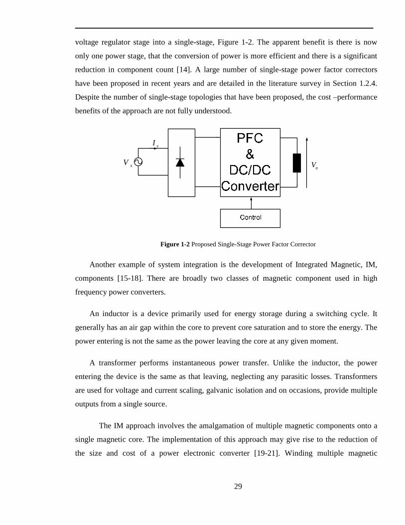
voltage regulator stage into a single-stage, Figure 1-2. The apparent benefit is there is now
only one power stage, that the conversion of power is more efficient and there is a significant
reduction in component count [14]. A large number of single-stage power factor correctors
have been proposed in recent years and are detailed in the literature survey in Section 1.2.4.
Despite the number of single-stage topologies that have been proposed, the cost –performance
benefits of the approach are not fully understood.
sV
sI
oV
Figure 1-2 Proposed Single-Stage Power Factor Corrector
Another example of system integration is the development of Integrated Magnetic, IM,
components [15-18]. There are broadly two classes of magnetic component used in high
frequency power converters.
An inductor is a device primarily used for energy storage during a switching cycle. It
generally has an air gap within the core to prevent core saturation and to store the energy. The
power entering is not the same as the power leaving the core at any given moment.
A transformer performs instantaneous power transfer. Unlike the inductor, the power
entering the device is the same as that leaving, neglecting any parasitic losses. Transformers
are used for voltage and current scaling, galvanic isolation and on occasions, provide multiple
outputs from a single source.
The IM approach involves the amalgamation of multiple magnetic components onto a
single magnetic core. The implementation of this approach may give rise to the reduction of
the size and cost of a power electronic converter [19-21]. Winding multiple magnetic

30
components onto a single core is not difficult, however the analysis, understanding and design,
of such devices is complex.
The concept of integrating various magnetic components onto a single core is not a recent
proposal as seen in [22-26]. An IM appears in numerous guises such as coupled inductors,
which can exploit the phenomenon of current ripple steering [27] and ripple cancellation [28],
or integrated transformers, that is two or more transformers on a single core, and finally
integrated magnetics, the implementation of an inductive component and a transformer on the
same core. The motivations for such approaches are to reduce the overall circuit component
count, cost and to take advantage of any inherent functionality that arises with these methods
[21].
It is not only the emergence of new design techniques and methods that is driving the
development of power converter topologies, but also the emergence of new applications such
as high power light emitting diodes, HP LEDs, [29]. The key characteristics of HP LEDs are;
excellent reliability, instant turn on, dimmability, long life, approximately 50,000 hours, good
colour and temperature rendering. Their efficacy is typically 100 lm/W in 2010, with
manufacturers indicating that this value will improve [30].
The drive towards ever more powerful and adaptable, yet efficient, street luminaire
systems is forcing the lighting industry to adopt new technologies. The most common street
lighting systems today utilise high intensity discharge lamps, often Low Pressure Sodium,
LPS. These lamps currently provide the highest optical output per unit of electrical input, 200
lm/W [31]. However, the amber colour of light that LPS lamps emit is not the most conducive
for night lighting and white light has been shown to be the most beneficial in terms of obstacle
perception, security and driver’s reaction times [32, 33]. High Intensity Discharge, HID, lamps
that emit white light are usually metal halide and have an efficiency of around 90 lm/W.
However, these lamps take a number of minutes to reach ideal operating temperature and
maximum efficiency, are not easily dimmable and have a maximum useful operating life time
of 12,000 hours [31]. Street lamps in Europe currently burn on average for 4000 hours per
year. This equates, for a typical city of 18000 lamps, each consuming approximately 150 W,
to an electricity consumption of 11 GWh per annum.
31
Unlike conventional power or signal diodes, HP LEDs cannot be subjected to
significant reverse voltage, 3V is typically the limit without irreversible damage occurring
[34]. The simple option of connecting anti-parallel LED strings to the mains through current
limiting impedances is not advisable since a severe 100 Hz optical flicker can occur, causing
stroboscopic effects [35]. Stroboscopic effects are a serious issue for the lighting industry,
since migraines and epileptic fits have been attributed to this phenomenon [36]. Optical
illusions can occur, as rotating machinery subjectively appears to be stationary or apparently
moving in an opposite direction, due to temporal aliasing [37, 38]. Additionally, closed-circuit
television, CCTV, equipment can be affected if the refresh rate is not synchronised correctly,
thereby corrupting the recorded image.
There are a number of commercially available solutions for driving high power LEDs.
They broadly fall into the following categories; low power, <10 W indication lighting and
illumination, medium power ≈ 20 W, halogen and spotlight replacements or indoor lighting,
and finally high power 40-80 W, outdoor illumination and architectural lighting. To achieve
the luminance level of a street light, typically 10,000 lumens, using HP LEDs requires a power
supply that can deliver 180 W.
The requirements of this power supply would not only be to regulate the power to the
HP LEDs, limit line harmonic currents and minimise total harmonic distortion, but achieve a
long operational lifetime, comparable to the lifetime of the HP LEDs themselves. Therefore a
string of LEDs supplied from the mains must be connected via an AC/DC converter regulator,
to protect them from reverse voltage and mains voltage surges, a power factor corrector stage
and a current regulating stage.
The light output from an HP LED is directly proportional to the device’s forward
current [39]. To ensure good control of light output and equal current through each LED, it is
desirable to have the LEDs connected in a series string, and to control the current through the
string so that it is constant despite mains voltage changes, see Figure 1-3.

32
sV
sI busV
V0
Figure 1-3 LED PSU block diagram
To achieve a long operational lifetime and overall system robustness, the PFC
converter and current regulator must be able to operate for 50,000 hours. Typically, the life
limiting factor for a switched mode power supply is the electrolytic capacitor that is used for
voltage ripple limiting and energy storage. These devices degrade rapidly compared to HP
LEDs, having a typical operating life of 7,000 hours [40], and are not suited for applications
which are exposed to large ambient temperature variations, -40 C to +40 C, to which street
lighting is subjected [41, 42]. However, inside a luminaire the upper temperature may reach 85
C or more. There are electrolytic capacitors with longer lifetimes, 60,000 hours [43], however
these are large and expensive. For an extended lifespan and low cost for the regulator, this
component is not suitable.
Alternative capacitor technologies such as ceramic or metallised film are more suitable
in terms of operational lifetime, [44] but they do not have the same charge storage capacity as
an electrolytic device. In order to achieve a single 180 W HP LED driver, the power factor
correction stage must limit line harmonic currents, minimise total harmonic distortion, all
without the use of an electrolytic capacitor, whilst providing sufficient energy storage during
the twice per cycle voltage zeros. Further, the elimination of the electrolytic storage capacitor
not only impacts upon the power quality but may also result in additional demands on the
control system performance.
By addressing these issues, the inherent capabilities of HP LED lighting can be
exploited to provide benefits such as reactive lighting (dimmability), increased lumens per
watt, and identification of luminaire failure/performance through intelligent communication.

33
Considering that street lighting authorities are obliged to pay a tariff for low power factor,
ideally the fundamental component of the current should be in phase with the voltage to
minimise cost. These techniques can all help reduce the current yearly carbon emissions of
street luminaires.
1.2 Literature Review
The objectives of this section are to review the issues detailed in Section 1.1 and how
current techniques and topologies can be implemented to address them. Power factor
correction techniques are reviewed along with research being conducted to develop single-
stage power factor correctors. Integrated magnetics methods are explored to see how this
approach can further enhance a power topology. A review of control approaches and
requirements is detailed for topologies operating as power factor correctors or voltage
regulators. The characteristics of HP LEDs are reviewed along with the operational
requirements and key issues of the HP LED driver. Finally a discussion of modern power
electronic devices is conducted.
1.2.1 Power Factor Correction Techniques
A review of passive and active power converter topologies approaches follows. These
circuits ensure a high PF and limited line current harmonics. The review is not an exhaustive
list of topologies, but serves to provide a fair and representative selection.
As introductory texts to this subject, five particular publications highlight the general
aspects and themes of the fundamental principles of power factor correction and power
conversion techniques [8, 10, 45-47]. These references discuss the fundamental theory and
analyses of power factor correction methods, and in particular highlight the two main
approaches utilised when limiting unwanted harmonic currents and poor power factor. These
solutions fall into two general categories; passive power factor correction and active power
factor correction.
1.2.2 Passive Power Factor Correction
Passive power factor correction is the simplest and most reliable way of improving the
power factor of a load. Passive PFC approaches can be categorised as either AC side or DC,
post rectifier, approaches.

34
The less common approach of AC side PFC is an LC filter in series with the mains
input. Figure 1-4 (a) shows this arrangement, the distortion in the line current is reduced by
adding a large inductance. However, the output voltage, power and power factor will be
reduced, due to the added series impedance. Figure 1-4 (b, c) shows resonant pass and
resonant trap circuits that are sensitive to both frequency and load [48].
sV
sI
dcV
dcI
Figure 1-4 Passive power factor correction (a) AC side LC filter, (b) Parallel resonant PFC, (c) series
resonant PFC, (d) DC side LC filter
The parallel resonant tank filter presents an infinite impedance to the third harmonic
input current, resulting in a lower value of input peak current. An alternative approach is the
series resonant filter that is designed to be resonant at the mains frequency. The quality factor,
Q, is high in this method and the impedance of the circuit is high at frequencies far from the
mains frequency, so that only mains frequency currents may pass, resulting in a near unity
power factor. The most common passive approach is DC side PFC, after the AC rectifier
diodes, Figure 1-4 (d). The maximum output power is independent on the inductance value,
but the distortion cannot be reduced below 48% [11].
Other passive PFC approaches, such as the Valley-Fill approach [49], rely on the use
of additional diodes and capacitors to change the effective circuit at various stages of the
charge and discharge cycle. This topology is not strictly passive, as there is no LC filter, but it
can be considered such as due to the passive switching action of the additional diodes.

35
The passive PFC approach can be further adopted to incorporate other functions such
as integrated EMC control. The power electronic devices utilised in a power switching
systems inherently produce electromagnetic interference, which can be transmitted by:
radiation and conduction. To attenuate these unwanted effects, the topology presented in [50]
attempts to integrate the functionality of a passive PFC and an EMC filter as one stage.
1.2.3 Active Power Factor Correction
The more common approach to perform PFC is to actively shape the input current, sI ,
to be as near sinusoidal and in phase with the input voltage, sV , as possible. In principle, if
there is zero displacement between sI and sV , and the current is sinusoidal, then a purely
resistive load is emulated, the conditions for unity power factor are satisfied.
The boost converter can be considered to be the most basic topology in use for active
power factor correction and is also the most commonly implemented. The fundamental
operation of this configuration as a power factor corrector is detailed in [10, 45, 46]. The
converter can operate in Continuous or Discontinuous Current Mode, CCM / DCM
respectively. A CCM boost PFC converter can easily achieve unity power factor, however
there is a requirement for a large value of inductor, L , to maintain CCM in all operating
conditions, and a relatively complex control circuit, see Section 1.2.5.
Operating in DCM however, can eliminate the need for a complex control circuit and
reduce the size of the inductor [51]. Control circuit simplification is due to the inherent
characterisitcs of the DCM. By analysing the input current in the discontinuous mode, the
average current across a switching cycle is approximately proportional to the input voltage.
Therefore if the duty ratio is constant throughout a line cycle, the circuit has a constant input
resistance characteristic, the input current therefore tends to track the variations in input
voltage [52]. Moreover, since the inductor current is zero before the start of the next switching
cycle power loss is reduced, particularly diode reverse recovery loss, due to zero current
switching, ZCS. This is the case for all active PFC converter topologies operating in DCM.
The boost PFC has the merits of high power conversion efficiency and low total
harmonic distortion, THD, but it generates a higher DC voltage at its output, DCV , compared to
the input voltage, sV . This is an advantage since it allows the input current to be shaped over

36
virtually the full utility line cycle. Some applications however may require a lower DCV , in
which case the boost topology alone would be unsuitable.
Another conventional topology suitable for PFC, is the buck converter [45, 53]. Like
the boost topology, the buck converter is a highly efficient converter when operating in CCM.
But other attributes are its ability to limit inrush currents, prevent short circuit conditions
between line and output and obtain a lower DC output voltage with respect to its input.
However to achieve CCM and low output current ripple tends to require a physically large
inductor, often leading the buck converter to be dismissed as a PFC converter. Finally, the
buck converter, like the boost has the ability to operate in DCM.
In the buck-boost converter, the output voltage can be higher or lower than the input
voltage [45, 47], albeit inverted. In universal input PFC applications, this ability to both step-
up and step-down DCV , is a major attraction. Cascading a boost converter and a further down-
stream buck converter can achieve the same outcome, but at a cost of a lower efficiency as the
power is processed twice. The buck-boost also has similar attributes to the buck converter, as
it has the ability to limit inrush current and prevent against over current conditions during
short circuits. Finally, like the previous converters the buck-boost has the ability to operate in
either CCM or DCM.
However the quality of the input current waveform and the ability to perform PFC
differs greatly between the circuits [5]. Figure 1-5 shows the input current-voltage
characteristics for a discontinuous current mode boost converter. It can be noted, that as long
as the output voltage, DCV , is larger than the peak of the line voltage, sV , then the correlation
of Vs and Is is near linear. The non-linearity is due to the fall time, swTδ , of the inductor
current to zero, which varies over a input line cycle, The effects of the non-linearity can be
reduced by increasing DCV with respect to sV , which diminishes swTδ [5, 54].

37
DCVsI
t
t
sV
sI
sV
DCV
Figure 1-5 DCM boost converter input I-V characteristics
Unlike the boost converter, the buck-boost inductor is not always electrically
connected to the line supply, therefore the fall time of the inductor, swTδ , is not seen by the
line input. The average input current of this converter is seen in Figure 1-6. It shows a linear
relationship between Is and Vs. This in turn forces the Is to be sinusoidal and in phase with Vs
and with a near unity power factor.
t
t
sI
sV
sI
sV
DCV
DCV
Figure 1-6 DCM Buck-boost input I-V characteristic
Automatic input current wave shaping is not without its issues, as the DCM inductor is
relatively small and the power semiconductor devices are subject to larger switching current

38
and voltage stresses, which can limit the power throughput. Techniques such as interleaving is
one approach to increasing this power limit [55, 56].
As well as limiting the input current harmonics and ensuring a low total harmonic
distortion of the line current, the PFC stage also provides a means of energy storage [57]. The
power flow into the energy storage capacitor, C, in Figure 1-7, is not constant, but is a sine
wave at twice the line frequency, since the power is the instantaneous product of the rectified
line voltage, Vrec, and current, Irec. The output capacitor stores energy when the absolute
instantaneous value of sV is higher than DCV and releases the energy when the instantaneous
value of sV is lower than DCV , in order to maintain a constant power flow. This flow of energy
in and out of C, results in a DCV ripple voltage at the 2nd harmonic.
sV
sI
CP
CI
2π/2π π
DCV
Figure 1-7 Energy storage performed by PFC capacitor
1.2.4 Single-Phase Single-Stage Power Factor Correction
The approaches discussed in the previous sections relate to achieving the harmonic
specifications shown in [1], high power factor and second harmonic energy storage. However,

39
most practical applications require a further conversion of this intermediate voltage. A second
converter stage is often used for fast dynamic regulation of output voltage, used to step up or
down the voltage, and to limit voltage or current ripple to desired requirements. The most
common approach is to cascade a second switching DC/DC converter to regulate the output
voltage and current ripple as seen in Figure 1-1. As these two power stages are controlled
separately, optimisation of the two power converters, in terms of high power factor and fast
output voltage regulation, is possible. However, the two-stage approach has the disadvantage
of increased cost and physical size due to the component count and the two control circuits
[58]. The block diagram also implies that the power is processed twice, reducing the overall
efficiency.
The single-stage approach for addressing power factor correction is depicted in Figure
1-2. It can be seen, the major advantage of this method is not only the power being apparently
processed once but, more significantly, only one control block is required reducing the
component compared with the two-stage approach.
A large number of single-stage PFC circuits have been proposed in recent years, and
this section aims to present a representative survey. The concept of single-stage power factor
correction converters dates back to [59]. The converter presented is a single phase offline
converter providing independently controlled dual outputs, but has the disadvantages of a high
component count. It suffers wide switching frequency variations and high voltage stresses. It
nevertheless integrates a PFC converter with a cascaded DC/DC converter.
Many single-stage PFC converters are a cascaded combination of an input current
shaper converter and a DC/DC converter. In some the energy storage is in series with the
power flow, and in others the energy storage is in parallel with the power flow [60].
A common example of a series type single stage power factor corrector is the boost
integrated buck rectifier energy DC/DC converter, BIBRED, and the boost integrated flyback
rectifier energy DC/DC converter, BIFRED, proposed in [61, 62] and in Figure 1-8. These
converters are purely a cascaded connection of a boost converter performing the role of the
input current shaper, and either a buck or flyback converter performing the role of output
voltage regulation.

40
Despite their apparent simplicity in design, and the need for only one control loop, a
common operational failing with these converters is the DC bus voltage level, across Cb, at
high line voltage and low load conditions, which makes these converters, if unmodified,
unpractical to implement.
sVoV
oI
sI
sV
sIoV
oI
Figure 1-8 (a) BIFRED single-stage PFC, (b) BIBRED single-stage PFC
Numerous suggestions have been proposed to address this issue, in [63], a voltage
feedback concept is described to suppress the high voltage at light load conditions. In the case
of the BIFRED, an additional transformer winding is added in series with the discontinuous
current mode, DCM, boost inductor.
sV
sIoV
oI
Figure 1-9 BIFRED with series voltage feedback winding

41
This extra winding, Nfb in Figure 1-9, feeds back the intermediate bus voltage when the
boost inductor is energised, and as a consequence the input power can automatically be
reduced, whilst maintaining the peak bus voltage within a satisfactory range. Based on this
technique, the authors have derived several new single-stage PFCs based on a DCM boost
converter. Despite the reduced bus voltage, the input current waveform is degraded due to the
inductor current dead region caused by the additional feedback windings.
Other methods proposed to reduce the high voltage stresses are presented in [62, 64],
are to modulate the switching frequency. The DC voltage transfer function of the CCM
DC/DC converter depends only on the duty cycle to regulate the output voltage, and the DC
voltage transfer function of the DCM input current shaper cell depends singularly on the
switching frequency. It is therefore now possible, by varying the switching frequency, the
intermediate bus voltage can be regulated without effecting the converter output. The penalty
of such an approach is that often a large frequency range is required which makes it difficult to
optimise wound components.
Alternative single stage PFC converter topologies are detailed in [54]. Similar to
earlier converters, this approach is a cascade of two already existing converters, a boost and
forward converter. Figure 1-10 shows there are now two primary windings connected with
separate bulk energy storage capacitors in series with the isolation transformer of the DC/DC
stage. This arrangement implements a series charging when the switch is on, and a parallel
discharging of the capacitors when the power semiconductor is turned off. The results of these
actions effectively introduce a ‘two-to-one’ voltage division on the original single storage
capacitor. Analysis by [65], shows that the bus capacitor voltage can be maintained within 250
V of the peak line voltage, therefore enabling the adoption of low voltage components.

42
oV
oI
sV
sI
Figure 1-10 Cascaded single-stage PFC with two switch DC/DC converter
Besides the topological manipulation of the common boost and buck type approaches
to series type power factor correction, the Cuk and Sepic converters have also been adapted to
operate as a single stage power factor correctors [66-68].
The power imbalance and high bus voltage caused by the combination of DCM input
current shapers and CCM DC/DC converters is addressed in [68]. A new family of single-
stage, single switch PFC converters is introduced, that again cascade a boost type input stage
and buck type DC/DC converter. However in the topologies presented, the energy storage
capacitor is in parallel with the power flow, Cb in Figure 1-11. Furthermore the concept of
similar current conduction operation modes for both stages, to limit peak voltages across the
capacitor and power semiconductor components is introduced. In [68] it is suggested that both
stages should be operating in discontinuous current mode in order to limit stresses at light
load. In this state of operation, over the entire load range the DC bus voltage becomes
independent of the load. What’s more, the principle can be applied to other modes, continuous
conduction mode for both stages [58].

43
sV
sIoV
oI
Figure 1-11 Parallel capacitor in single-stage PFC BIFRED
Using the DCM approach for both stages is likely to result in lower efficiency because
of the higher conduction losses, and the common CCM approach generally has a lower power
factor and a high distorted input current waveform.
Development and optimisation of this family of converters is conducted in [69-72]. In
[73], it is proposed that to limit the maximum voltage, then the converters should be operated
in boundary current conduction mode, BCM. In this state the converters would be able to
adjust the operating mode according to the load conditions. It is found that the full load range
can be divided into the three modes of operation; DCM, CCM and BCM, determined by the
output condition.
Another parallel variation is proposed in [74], see Figure 1-12, again with the intention
of reducing the stresses that occur in the single stage approach. The converter is formed by
integrating a boost PFC with a two-switch clamped flyback converter. This topology
simultaneously provides good output regulation and a high power factor. The current stresses
in the two power switches are invariably lower than those of the single-stage, single-switch
approaches detailed earlier. Also a high PF is achieved due to the absence of ‘dead banding’ of
the input current at the input voltage zero crossing.

44
oV
oI
sV
sI
Figure 1-12 Single stage PFC converter prososed in [74]
The disadvantage of the parallel is the high component count, in which the multiple
semiconductor devices share the high voltage and current stresses. Also the control strategy
requires two loops to synchronise the switching components.
Recently, resonant converters have been proposed for single-stage PFC, [75-79]. To
date the single stage PFC topologies presented have been limited to a power range of <300 W,
for the reason that the topologies become too complex or the stresses become too great for
semiconductor devices.
sV
sIoV
oI
Figure 1-13 Single stage LLC PFC converter

45
The proposed converters comprise a series-parallel LLC three level resonant converter,
see Figure 1-13. This approach provides the opportunity to operate at much higher power
levels with the addition of lower voltage stresses. The topologies integrate the operation of a
boost converter for current shapers, and a three level LLC resonant converter. Despite
achieving an efficiency of upwards of 90 % at a power of 2.3 kW, the system again requires
two control loops. The output voltage is regulated by the switching frequency of the resonant
stage, and the DC bus is controlled by the duty cycle of the current shaper, which maintains a
near unity power factor.
1.2.5 Power Factor Correction Regulation Control Strategies.
Continuous current mode operation often uses a two-loop control strategy such as
average or peak current-mode control. The outer voltage loop senses DCV and delivers a
control signal to the inner current loop which is sensing the inductor current, IL, and actively
wave shaping the current Is to be sinusoidal and in phase with the input line voltage Vs [80].
Peak current-mode control operates by comparing the positive current slope of the
inductor with a predetermined reference level set by the outer voltage loop. When the
instantaneous inductor current reaches the reference level, the power switch is turned off.
Despite this approach being relatively simple to implement there are a number of issues. This
method is susceptible to jitter noise on the sensed inductor current [81]. Above transistor duty
cycles of 50 %, inherent instabilities create sub-harmonic oscillations regardless of the
switching topology. This can be compensated for by the addition of a ramp to either the sensed
inductor current or the current reference signal. However, at duty cycles near 90%, slope
compensation results in a significant deviation between the ideal reference and the actual
inductor current which may cause increased distortion of Is [82].
Average current mode control, unlike peak current mode control, has an additional
compensator [45]. The action of the current control loop forces the input current to match a
reference signal. The amplified current error is compared to a saw tooth waveform generated
by an external oscillator, to generate the PWM waveform. The gain bandwidth of the current
amplifier can be tailored for optimum performance allowing the current to track a near
sinusoidal waveform with a high degree of accuracy. This is claimed to result in a power stage
with excellent noise immunity and no requirement for slope compensation. The voltage loop

46
however must have a relatively narrow bandwidth, compared to the current loop, otherwise the
second harmonic output voltage ripple would result in a modulation of the input current, Is, to
keep the output voltage constant, therefore distorting Is [46].
Hysteretic control presented in [83], is another method for regulating VDC whilst
performing power factor correction. For a converter operating in CCM with a two loop control
system, the switch turns on when the inductor current falls below a predetermined minimum
level, and turns off again when the current goes above an upper limit, resulting in variable
frequency operation. This control approach does have the advantage that a compensation ramp
is not required, however the method is susceptible to noise due to the switching edges, also the
variable switching frequency makes magnetic design difficult to optimise [84], and finally, the
inductor current, IL, has to be sensed by some means.
An extension of hysteretic control is critical current mode control [85]. The inductor
current is allowed to fall to zero, at which point the switch is turned on until a predetermined
upper current level is reached. This approach allows the freewheeling diode to recover ‘softly’
as there is no recovery loss. Yet due to the near DCM operation the peak current levels tend to
be higher resulting in higher conduction losses.
In PWM control methods for converter topologies operating in DCM, the internal
current control loop can be eliminated, due to the automatic input current wave-shaping of
discontinuous mode converter, Section 1.2.3. The voltage mode control approach is presented
in [45]. Apart from the obvious advantages of a simplified control loop, and no current sensing
components, this method uses a constant switching frequency, allowing for simple design of
magnetic devices and EMC filtering. However, the circuit components are subject to higher
peak current levels than a continuous conduction converter.
The second harmonic output voltage ripple in a PFC converter the limits the achievable
dynamic response of the voltage control loop. To avoid loop instability, the voltage control
loop of all approaches mentioned previously, must have a unity gain cross over, cf , below the
line frequency. It is for this reason, that PFC converters have a poor transient response to line
and load fluctuations.

47
A number of modifications or enhancements to the voltage loop are proposed by [86],
including a notch filter which is designed to attenuate only the twice mains frequency ripple
component. This approach allows a very high power factor and a fast loop response to be
achieved, but presents some practical difficulties in its implementation. High component
tolerances are needed or a complex active tracking filter of the input mains frequency must be
implemented.
A similar approach to a notch filter would be to ‘sample and hold’ the output signal of
the voltage compensator. The voltage compensator processes the ripple frequency but the
propagation of the disturbance through to the PWM is eliminated [87]. The disadvantages of
this approach are the complexity of the control loop implementation, poor frequency response
of the closed loop, and the difficulty of undertaking stability analysis due to the non linearity
of the ‘sample and hold’.
The proposal in [86] to overcome the limitations caused by the second harmonic ripple
is the so called regulation band approach. Upper and lower voltage limits are determined, and
while DCV is between these limits the control loop does not attempt to regulate DCV . The
control loop is essentially open loop during this condition. If DCV were to exceed the limits
then the voltage loop would generate a signal that would force DCV to return to within the
regulation band. This approach is simple to implement and results in the removal of the low
frequency ripple from the feedback signal enabling a good power factor to be achieved. This
method is simple to implement, has a fast transient response when operating within defined
limits, however like the ‘sample and hold’ method there is a nonlinearity to contend with when
analysing stability.
One final approach to enhance the voltage loop is ripple cancellation [88], where the
reference voltage that is fed into the voltage compensator has a component superimposed that
has the same frequency but is 180 out of phase with the output voltage. Despite realizing a
fast transient response, practical implementation is difficult as the injected voltage has to
accurately reflect the sensed feedback voltage, if not the input current of the converter will be
distorted.

48
1.2.6 Magnetic Modelling and Integrated Magnetic Concepts
This section describes current integrated magnetic approaches, modelling techniques and
magnetic materials.
Integrated magnetic components are often seen in the guise of coupled inductors [89].
One particular application of coupled inductors is the method of interleaving power converter
stages to reduce input and output ripple elements and reduce the current level in individual
devices. Numerous authors operate these converters in DCM with direct coupling of the
magnetic devices [90-92].
One of the main aims of integrated magnetics however, is not only to reduce the magnetic
component count but also to achieve electrical gains. Different coupling methods realise
different behaviours. Inverse coupling can reduce RMS currents, the DC flux is eliminated and
the AC flux in the core is lower, whereas with direct coupling, the device shows increased
current ripple per phase, resulting in increased copper loss and no cancellation of the DC flux
component [17, 89, 93, 94]. Unfortunately an added series inductor is required for the inverse
coupling approach to filter the DC current component. A more common approach to magnetic
coupling is found in EMC suppression common mode filters [95].
Transformers with multiple input and output windings may be classed as integrated
magnetic devices and the concept can be developed further by combining inductive and
transformer components on a single core.
A number of methods have been proposed for the analysis of magnetic components. One
of the first proposed methods is that of the reluctance model. This approach is detailed in [15,
18, 96] and simplifies a magnetic structure into an equivalent electrical model. Since magnetic
flux lines are closed paths, the flux becomes analogous to current. The primary assumptions
are that the magnetic field is constant and is aligned to the direction of the path of integration.
Non-linear ferrous materials and points close to saturation are not taken into consideration.
A similar modelling approach to a reluctance model is the inductance model, which is
more useful as it converts the electromagnetic circuit into a purely electrical system [97]. To
form the inductance model, a persistence model must be created from the reluctance model
[26]. All parallel elements now become series elements and visa versa, and that all loops

49
become nodes, and nodes become loops. Each reluctance now becomes its inverse, a
permeance. All voltage sources become current sources and the flux behaves as voltage drop
across the respective permeances.
These methods are very effective for modelling separate magnetic components, but if
the topology or integrated magnetic is complex or one has to consider the non-linearity of the
ferromagnetic material then these methods can become unmanageable.
Another modelling method that can accommodate these non-linear effects and
parasitics, is the Gyrator-Capacitor approach discussed in [97-99]. A gyrator is an ideal two
port circuit element that reflects the impedance at one port as its reciprocal at the other, that is
a capacitance at one port is reflected as an inductor at the other port. The gyrators replace the
windings in this method and are represented as current controlled voltage sources. The core is
modelled using the reciprocal of reluctance, that is a permeance.
To assist with the selection of the core materials and shapes, [100] compiles a table of
the various magnetic materials and available core. Powder iron toroidal cores have a
distributed airgap to allow high energy storage, whereas ferrite materials have very low high
frequency loss characteristics [17].
New materials such as amorphous alloys allow for a much higher saturation flux
density, approximately 1.6 T at 25 C, compared to a ferrite, approximately 0.3 T at 25 C.
Despite the promising performance of these newer materials, they are invariably more
expensive and so not widely available at present.
1.2.7 Devices and Components
Rapid progress has been made in the development of high voltage devices,
semiconductor technology and capacitive components, through means of advanced processing
techniques and novel device structures. Device improvements have enabled topologies that
were previously dismissed, due to voltage/ current stress or cost, to become viable. The
driving factors for such developments are the ever present demand for increased power
density, low system cost and high reliability. This section reviews the current status, discusses
the future trends of device technology and their impact upon emerging topologies.

50
1.2.7.1 Power Diodes
Traditionally the most commonly used high voltage diode is the silicon PiN structure.
These devices typically have an on-state voltage drop of approximately 1 V which is
acceptable at high voltages but is significant for low voltage applications. Being a minority
carrier device, they have a poor reverse recovery characteristic arising from the large stored
charge in the drift region during forward bias. This reverse recovery can form a significant
contribution to the overall losses in the device and circuit, therefore limiting its use and
application, especially at high frequency. Other adverse effects of reverse recovery include
electromagnetic interference and thermal management. These devices are mature products,
and their limitations are well understood and acknowledged.
Numerous techniques are used to improve PiN diode characteristics, such as
optimising the doping profile in the epitaxial layer or by reducing the minority carrier lifetime
[101]. Typical PiN rectifier power diodes exhibit performances of 2000 V, 200 A with a
forward voltage drop of 1.25 V and reverse recovery times of approximately 25 ns. Any
further reduction in recovery times, requires an improvement to either the current technology
or a change of material.
An alternative to the PiN diode is the high voltage Schottky barrier diode, SBD. The
conduction current of Schottky barrier diode consists of majority carriers, therefore, unlike the
Silicon, Si, diodes, the stored charge is negligible and the diode turns off with a near zero
reverse recovery current [102]. The materials used in these devices are either GaAs, GaN, but
the leading candidate is Silicon Carbide, SiC. Superior electrical performance is achieved with
these materials compared with Si due to high breakdown field, high electron mobility and high
saturation velocity [103]. The material properties of SiC devices make it an ideal choice for
high power, high temperature and high frequency applications. Experimental evaluations of a
similarly rated Si diode and SiC diode in [103] reveal that despite elimination of switching
losses, due to the high forward volt drop, 3 V, associated with SiC SBD, conduction losses are
now the dominant loss factor.
Compared to Si diodes however, SiC material diodes can offer simplified power stage
design due to the elimination of snubbers, reducing component count. Furthermore the
reduction in power losses leads to lower operating temperatures, and reduced EMC emission

51
from switching transients. Cost however is a major barrier for market uptake, currently a 3
inch SiC wafer is 25 times more expensive that a Si wafer of the same diameter. Further SiC
substrates contain a much higher level of defects, which reduces yields.
As well as investigating the performance of different materials, various device
structures have been explored in order to improve device performance. Significant
improvements in the trade off between on-state voltage drop and reverse recovery has been
demonstrated by altering the injection efficiency using either a merged PiN/Schottky structure,
MPS [104], self adapting P-emitter diode, SPEED, structure [105] or a static shield diode,
SSD, structure [106]. These device structures provide a superior trade off curve between the
on state voltage drop and reverse recovery charge when compared to PiN diodes.
1.2.7.2 High Power Light Emitting Diodes
The development of high efficiency Indium Gallium Nitride, InGaN, blue Light
Emitting Diodes, LEDs, in the early 1990’s was a break through for the development of ultra-
bright white HP LEDs [107]. The spectrum of light generated by a white HP LED is shown in
Figure 1-14, along with the sensitivity of the human eye. The HP LED produces the visible
white spectrum by exciting an Yttrium Aluminium Garnet, YAG, phosphor layer placed over
the surface of a blue HP LED die, Figure 1-14. The die of the HP LED produces a blue to the
end of the visible spectrum near UV, of a wavelength at approximately 460 nm as seen in the
peak in the white HP LED spectrum at this wavelength [108]. The interaction between the
blue light and the phosphor produces visible radiation at longer wavelengths, approximately
500 to 750 nm through stokes shift [109].
The combination of blue light and phosphor generated light creates the perception of
white light. This approach currently has a luminous efficiency of approximately 100 lm/W
[108], however it is by no means the only way for HP LEDs to produce white light. Other
approaches include mixing the colour from individual red, green and blue LEDs. This
approach is the most efficient as no energy is lost in the Stokes Shift and enables a tuneable
white point. However, systems using this effect often employ feedback to stabilise the colour
produced. Another approach is for the LED die to generate UV light, at 300 nm wavelength,
which then interacts with red, green and blue phosphors. This method produces a very stable

52
white point and high colour rendering, but degradation of the HP LED package is rapid due to
the UV light damaging the phosphors [108].
Figure 1-14 Typical HP LED spectral distribution (solid) and standard luminous sensitivity of the eye
(dashed).
These three approaches have developed to the point that HP LEDs can be seriously
considered for replacing conventional halogen and incandescent lamps in general illumination
and street lighting. Voluntary European legislation regarding the phasing out of incandescent
bulbs by 2012 makes this approach ever more attractive [110].
The key characteristics of HP LEDs are excellent reliability, instant turn on,
dimmability, high operating hours, approximately 50,000, and good colour and temperature
rendering [34]. Their efficiency is typically 100 lm/W in 2010, and manufacturers indicate that
this value will improve. However, before wide spread adoption of the technology can be
embraced, there are a number of outstanding issues that need to be addressed.

53
Figure 1-15 Schematic of a high power white LED.
Despite consuming less power than conventional HID lighting for the same light
output, the advantages for implementation are not always clear cut. Currently, HP LEDs are
invariably more expensive in terms of initial purchase cost, as they are a new technology. But
as market penetration increases, this initial cost will reduce.
A more fundamental challenge is that of thermal management. Regardless of the
quoted high lumens per Watt of converted electrical energy to useful visible light by the
manufacturers, the die of a typical white HP LED can reach temperatures up to 185 C [111].
This operating temperature is not conducive for long life and low luminaire maintenance. HP
LED manufacturers quote a maximum operating junction temperature, Tj, of 85 C to ensure 70
% luminance after an operating life of 50,000 hours, Figure 1-16. When the illuminance falls
below 70 % of the initial light output the device is deemed to have failed. Therefore, to meet
the quoted lifetimes of the HP LEDs and prevent excessive light degradation, the thermal
conditions must be well regulated, and the die temperature must be kept within the
manufacturer’s specification [112-115].

54
Figure 1-16 Relative HP LED light output lifetimes at various temperatures [29]
Once the thermal energy has been conducted away from the semiconductor junction to
the attached heat sink, the energy must then be dissipated to the ambient environment. For
street lighting applications, natural convection is the most suitable way of transferring heat to
ambient, due to its simplicity and reliability.
1.2.7.3 MOSFET
Since the introduction of power MOSFETs in the early 1970s, there has been
continued development in the improvements in the power density of the device, which closely
reflect the advances achieved in power rectifiers, for example through the introduction of new
materials and device structures. The key characteristics of a MOSFET are high input
impedance, generally a low on-resistance, fast switching speeds and ruggedness [45].
The performance of the Si DMOSFET has approached its theoretical limit [101],
therefore other structures have been developed. Recently the UMOSFET has become
commercially available. This trench gate device has a superior channel density due to the
elimination of the JFET resistance present in the DMOSFET arrangement, allowing lower on
state resistances to be achieved. UMOSFET structures can be further developed to
accumulation, inversion and extended trench field effect transistors (ACCUFET, INVFET and
EXFET) [116, 117]. The primary features of these arrangements is that the trench UMOS gate
extends in to the N substrate, and into the N+ substrate in the case of the EXFET. In this design
approach the current conduction occurs along the surface of an accumulation inversion layer
formed along the trench sidewalls, resulting in extremely low on resistance. Of this series of

55
structures the ACCUFET has the lowest of on resistances. Further the ACCUFET has the
advantage that it does not contain any parasitic P-N junctions.
Semiconductor material development that has greatly improved the performance of
high power diodes has also been applied to MOSFETS. SiC power devices offer substantial
performance improvements over Si, enabling increased power density, high efficiency and
higher temperature operation [102].
SiC MOSFETs were first proposed in the early 1990s [118], these power devices were
the vertical trench structure, UMOSFET. This construction is attractive due to its straight
forward fabrication, however the electrical performance of the DMOSFET SiC is far superior.
Due to higher bandgap of the material, SiC MOSFETs are achieving voltages approaching
1800V [118].
Whilst engineering samples of some devices are starting to become available, there are
a number of areas that need addressing such as the improvement of the Si02- SiC interface.
Reliability issues have been noted of the gate oxide under high field conditions. A second
issue with SiC power MOSFETS is the low inversion channel mobility. This is the result of
the high density of interface states present in the upper half of the bandgap [119]. In [120,
121], annealing with NO and N2O can relieve this issue slightly, but inversion channel
mobility in SiC remains approximately a order of magnitude less than in a Si MOSFET.
1.2.7.4 Capacitors
Technological developments in the semiconductor devices such as diodes and
MOSFETs have generally gone hand in hand. However such progress in capacitor technology
has not been so rapid. A wide range of capacitor types and technologies is available, and the
most common are listed in Table 1-2 along with their typical performance figures.
Electrolytic capacitors, wet or solid types [44], are the most suitable for addressing DC
filtering and energy storage. Limitations of these components include a significant equivalent
series resistance, ESR, which may increase under high current ripple conditions and high
temperature. This could compromise the filtering performance of the capacitor or may lead to
control loop instability in some power supply applications. The relatively short life time of

56
these capacitors is a serious concern in many applications, furthermore, the lifetime falls
rapidly at increased operating temperatures.
Table 1-2 Capacitor table comparison
Capacitor Type
Capacitance
Voltage (V)
Expected Lifetime
(hrs)
Temperature ( Cο )
Aluminium Electrolytic
0.1 µF - 1500 µF 2 to 500 7,000 -55 to +125
Ceramic 0.01 pF - 27 pF 2 to 500 k 50,000 -60 to +125 Film 0.5 pF - 30 pF 2 to 300 k 50,000 -40 to +85
Tantalum 1 nF - 9100 pF 2 to 2 k 2,000 -55 to +125
Ceramic capacitors types are often used for high frequency filtering and EMC [122].
The IEC 60384-8 and IEC 60384-9 classify these capacitors into two types, Class 1 and Class
2 respectively. Class 1 capacitors are required for frequency compensation of control loops,
coupling and decoupling in high-frequency circuits where low losses and narrow capacitance
tolerances are required. Class 2 capacitors are again used as coupling and decoupling
capacitors, but where higher losses and a reduced capacitance stability are demanded.
Film capacitors fulfil a number of roles, from general filtering, snubbing applications,
noise suppression, high voltage high frequency applications to more specialised applications
such as mains filtering, or filtering between mains line and earth, known as X and Y capacitors
respectively. Film capacitors may be either film/foil wound or metallised film types and use
materials such as; polyester, polyphelyne sulphide, polypropylene, and polyester
polypropylene [122]. Film/foil capacitors consist of two metal foil electrodes that are
separated by a thin insulating plastic film. Features of such devices are high insulation
resistance, excellent current and pulse capability as well as good capacitance stability. For
metallised film capacitors, the capacitor plates consist of aluminium sprayed onto the
dielectric surface by thin-film vacuum deposition. This process allows a smaller device, lighter
weight and lower ‘self healing’ due to an internal short circuit from an overvoltage transient or
device fault. Though suffering no permanent damage, capacitance may be reduced.
Tantalum capacitors are found in two forms, wet and solid. Wet electrolytic tantalum
capacitors are preferred in applications where there is the requirement for stable electrical
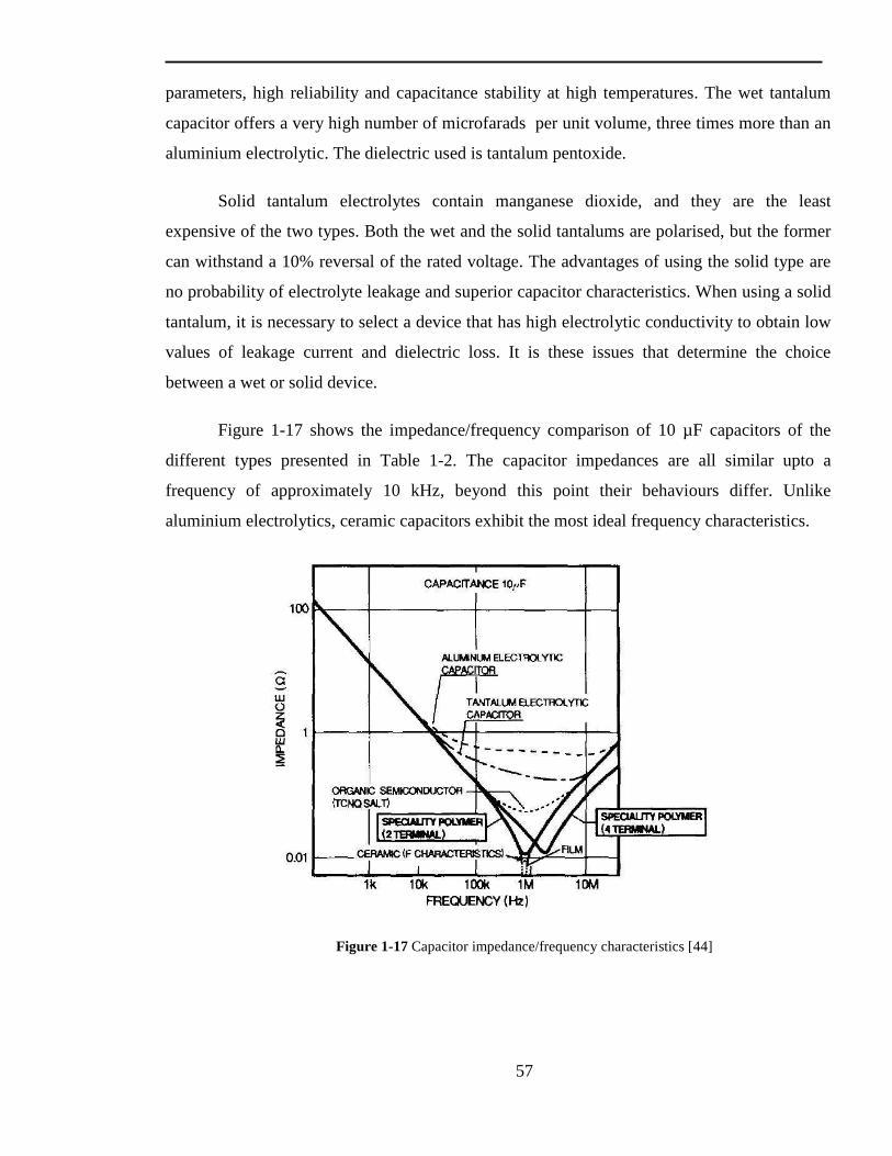
57
parameters, high reliability and capacitance stability at high temperatures. The wet tantalum
capacitor offers a very high number of microfarads per unit volume, three times more than an
aluminium electrolytic. The dielectric used is tantalum pentoxide.
Solid tantalum electrolytes contain manganese dioxide, and they are the least
expensive of the two types. Both the wet and the solid tantalums are polarised, but the former
can withstand a 10% reversal of the rated voltage. The advantages of using the solid type are
no probability of electrolyte leakage and superior capacitor characteristics. When using a solid
tantalum, it is necessary to select a device that has high electrolytic conductivity to obtain low
values of leakage current and dielectric loss. It is these issues that determine the choice
between a wet or solid device.
Figure 1-17 shows the impedance/frequency comparison of 10 µF capacitors of the
different types presented in Table 1-2. The capacitor impedances are all similar upto a
frequency of approximately 10 kHz, beyond this point their behaviours differ. Unlike
aluminium electrolytics, ceramic capacitors exhibit the most ideal frequency characteristics.
Figure 1-17 Capacitor impedance/frequency characteristics [44]

58
1.2.8 Street Lighting Considerations and Regulations
The regulatory requirements for street lights are summarised in this section. The
classification of lighting types and location, motorways or strategic routes, detailed in [123],
determines the optical requirements and light output performance of a street luminaire. Optical
requirements detail the lighting quality such as control of glare, colour temperature, colour
rendering, lifetime and illumination footprint, [42]. The level of illuminance for the route type,
leads to the selection of lamp type and overall operating power level.
A general code of practice for designing street lights is covered in [124].
Considerations such as weight, dimensions, chassis material, appearance, vibration levels, and
resistance to heat and fire are all detailed. This regulation also stipulates the accessibility of
the power converter and lamps should the need arise for servicing or replacement. To protect
the electrical connections and components [125] dictates that the system must be sealed to
water and dust ingress and have a degree of protection to IP56 rating. The thermal design of
the luminaire and its housing is also important since much of the electrical input power will be
dissipated as heat, for example, to achieve a typical street light output of 12,000 lumens,
approximately 150 LEDs are needed with a total power of around 180 W. Little of this 180 W
is converted to optical power, and so it can be assured that most of the 180 W is converted to
heat.
1.3 Summary of Literature Review
The main developments in the areas of single-stage power factor correction techniques,
integrated magnetics and high power light emitting diodes are summarised. Non-isolated,
passive and active PFC approaches are described. Active PFC methods produce the most
sinusoidal input current and highest power factor. Numerous control approaches are detailed
including current and voltage mode control. But the review suggests that there is no one single
control approach suitable for all requirements. The concept of single-stage power factor
correction is discussed. A vast amount of literature has been produced on this topic, and a
number of complex topologies have been developed. However the most effective and simplest
approaches are the topologies that have purely combined existing power converters. Integrated
magnetic approaches are outlined, whereby a number of different magnetic devices are
combined onto a single core, the associated modelling techniques, magnetic materials and core

59
structures are described. The development of advanced power components also stimulates the
development of power electronic approaches and control techniques. The emergence of high-
power light-emitting diodes is described which opens up the opportunity of making more
efficient lighting systems, however this also creates new, demanding requirements for the
associated power conditioning equipment.
With the ever growing demand for power electronic equipment to be more power
dense and have a lower component count, the idea of single stage power factor correction
appears to offer an attractive solution. However there is little published material with regards
to an integrated magnetic component being used within a single-stage power factor corrector
and its cost analysis. Secondly, with the emergence of HP LEDs and their superior operating
characteristics, the literature review clearly indicates that the electrolytic capacitor needs to be
eliminated from the associated power supply in order not to compromise the overall system
lifetime. This however has an impact upon the control approach and the ability to meet input
harmonic standards. Therefore it was decided to develop a HP LED driver that would fulfil
these requirements.
1.4 Thesis Structure
Chapter 2 details the analysis and design of a single stage power factor corrector with
an integrated magnetic component. The operation of the converter is analysed and a theoretical
design is performed. The integrated magnetic component is designed and wound, and a
SABER simulation is conducted of the S4PFC and the IM. The SABER results confirm the
analysis and design work.
Chapter 3 examines the dynamic behaviour and control requirements of the S4PFC
with an IM. The line-to-output and control-to-output characteristics of the converter are
examined with the aim of identifying a suitable control approach. The design of the control
loop is conducted and SABER and MATLAB simulations are performed to verify the control
design.
Chapter 4 details the experimental verification of the S4PFC. A prototype converter is
developed and the laboratory setup is explained. Electrical schematics and printed circuit
board layouts are shown, along with the results of the steady-state and dynamic experimental

60
testing. A discussion of the results is included along with the impact, performance and cost
benefits of this approach.
Chapter 5 describes the analysis and development of a power converter for a high-
power white-light emitting diode street light. A suitable topology is identified that can perform
without an electrolytic capacitor to fulfil the requirement to operate for 50,000 hours. The
operation of the converter is discussed and a theoretical design is performed. SABER
simulations are conducted to verify the design.
The identification and analysis of the control approach for the HP LED driver is
described in Chapter 6. The principles of operation and design are explained. The dynamic
performance of the selected control approach is explained to determine its suitability for this
application.
Chapter 7 details the experimental verification of the HP LED driver. A prototype
converter is developed which includes the constant current converter required regulate the
current through each of the individual LED strings. Electrical schematics and printed circuit
board layouts are shown along with the laboratory setup. Results of the steady-state and
dynamic testing are presented and discussions of the results are included.
Finally Chapter 8 presents the key conclusions of the thesis, detailing the contributions
of this research and the recommendations for further work.

61
2 Single-Stage Single-Switch Converter Analysis with Integrated Magnetic
2.1.1 Introduction
This chapter details the analysis and design of a Single-Stage Single-Switch Power
Factor Corrector converter, S4PFC, with an Integrated Magnetic component, IM. The power
topology is based upon a boost converter operating in Discontinuous Current Mode, DCM, for
Input Current Shaping, ICS, and a cascaded forward converter for output voltage regulation.
The steady-state operation of the converter is detailed, as well as the essential design
equations. MATLAB and SABER simulations characterise the steady-state performance of the
converter and verify the design equations. Analysis of the IM is performed, design methods
identified and its expected operation detailed, which is also verified using SABER
simulations.
2.1.2 Principles of Operation of S4PFC
A steady-state analysis of the single-stage single-switch power factor corrector is
detailed in this section. For simplicity, the following assumptions are made: all of the devices
and components are ideal, and the switching frequency, swf , is much higher than the line
frequency, linef . Figure 2-1 shows a schematic of the S4PFC, a boost converter is combined
with a forward converter forming the single-stage converter proposed in [68].
sVoV
oI
sI
BV
QI
BLI
QV
recV
Figure 2-1 Single-stage, single-switch power factor corrector with an integrated magnetic component
To achieve a high power factor, the boost converter operates in discontinuous current-
mode resulting in automatic shaping of the input current, Is, whilst the duty ratio, D, regulates
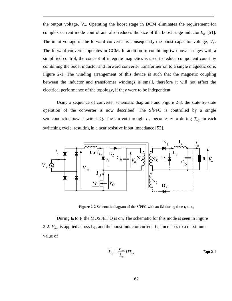
62
the output voltage, Vo. Operating the boost stage in DCM eliminates the requirement for
complex current mode control and also reduces the size of the boost stage inductorBL [51].
The input voltage of the forward converter is consequently the boost capacitor voltage, BV .
The forward converter operates in CCM. In addition to combining two power stages with a
simplified control, the concept of integrate magnetics is used to reduce component count by
combining the boost inductor and forward converter transformer on to a single magnetic core,
Figure 2-1. The winding arrangement of this device is such that the magnetic coupling
between the inductor and transformer windings is small, therefore it will not affect the
electrical performance of the topology, if they were to be independent.
Using a sequence of converter schematic diagrams and Figure 2-3, the state-by-state
operation of the converter is now described. The S4PFC is controlled by a single
semiconductor power switch, Q. The current through BL becomes zero during offT in each
switching cycle, resulting in a near resistive input impedance [52].
sVoV
oI
sI
BV
QI
BLI
QV
recV
oLI
Figure 2-2 Schematic diagram of the S4PFC with an IM during time t0 to t1
During t0 to t1 the MOSFET Q is on. The schematic for this mode is seen in Figure
2-2. recV is applied across LB, and the boost inductor current BLI increases to a maximum
value of
ˆB
recL sw
B
VI DT
L= Eqn 2-1

63
where D is the duty ratio, swT is the switching period and Vrec is the rectified input voltage.
During this period 1 BD LI I= .
During this time diode D2 is reversed biased by the boost capacitor voltage, VB, as CB
is discharged through the primary windings, NP, of the transformer. The peak current of
winding Np is
,
,
ˆˆ ˆs
p p mag
LL L
p s
II I
N= + Eqn 2-2
where Np,s is the turns ratio of the transformer primary and secondary windings, and ,
ˆP magLI is
the peak magnetising current of NP which is determined by
,
ˆP mag
B swL
p
V DTI
L= Eqn 2-3
where Lp is the magnetising inductance of Np. The total current through MOSFET, Q, is
determined by
1 PQ D LI I I= + Eqn 2-4
where 1DI is the current through D1 and
PLI is the primary winding current.
Noting the dot notation of the transformer windings, the peak current, SLI of the
secondary transformer windings is
( ), ,ˆ ˆ ˆ ˆ
S P P mag OL L L p s LI I I N I= − = Eqn 2-5
ˆoLI is the peak current through the output inductor, Lo.

64
BLV
BLI
QV
QI
1DV
1DI
ˆBLI
QV
QI
1
ˆDI
swDT (1 ) swD T−
0t 1t 2t 3t 0 swt T+
BV
2DV
2DI
PLV
2
ˆDI
,P magLI
PLI
sLV
sLIˆ
sLI
,
ˆP magLI
ˆPLI
,P magLI
swDT (1 ) swD T−
0t 1t 2t 3t0 swt T+
rLV
rLI
oLV
oLI
oCI
ˆrLI
oLI∆
swDT (1 ) swD T−
0t 1t 2t 3t0 swt T+
ˆoLI
Figure 2-3 Key waveforms of the S4PFC with an IM

65
Due to its orientation the secondary reset winding, Nr, during this time and the peak
voltage across this winding is determined by Eqn 2-6
,ˆ
rL B p rV V N= Eqn 2-6
where Np,r is the turns ration of the transformer primary and reset winding
During time t1 to t2, Q is turned off. The schematic for this mode is shown in Figure
2-4. The boost inductor charges the boost capacitor, CB, diode, D2, is forward biased and the
transformer magnetising energy escapes through Nr to the load.
sVoV
oI
sI
BVBLI
recV
Figure 2-4 Schematic diagram of the S4PFC with an IM during time t1 to t2
The voltage VQ across the transistor during this period is the boost capacitor voltage
plus the voltage referred from the conducting reset winding.
,
oQ B
p r
VV V
N= + Eqn 2-7
where Vo is the output voltage of the S4PFC. D1 is reversed biased by the primary voltage. The
time taken for BLI to fall to zero may be calculated as
2 1
ˆ
( )BB L
swB rec
L It t T
V Vδ− = =
− Eqn 2-8
where δ is the proportion of the switching period for BLI to fall to zero.

66
The voltage across winding Nr forward biases diode D5, allowing the energy stored in
the magnetic core to be transferred to the output of the S4PFC. The peak current in the reset
winding at t1, ˆrLI , may be written as
,
,
ˆˆ p mag
r
L
Lp r
II
N= Eqn 2-9
Eliminating ,
ˆp magLI using Eqn 2-3 results in
ˆr
B swL
p r
V DTI
L L= Eqn 2-10
As with a conventional forward converter, PN and SN are not conducting, and diode
D3 is reversed biased, which enables diode, D4, to freewheel and conduct the current oLI .
During time t2 to t3 Q is still off, BLI is zero and the current
rLI in the reset winding
continues to fall, reaching zero at time t3. The circuit configuration for the converter during
this period can be seen in Figure 2-5.
sVoV
oI
sI
recV
oLI
Figure 2-5 Schematic diagram of S4PFC with an IM during time t2 to t3
The reverse voltage across D1 is
1
,
oD
p r
VV
N= Eqn 2-11

67
The off state voltage across VQ is
,
oQ B
p r
VV V
N= + Eqn 2-12
The reverse voltage across diode D2 is
2D B recV V V= − Eqn 2-13
During the brief time period from t3 to t0+Tsw diode D4 is still conducting the
freewheeling current of Lo, and there is no other current flow in the circuit. VQ is now equal to
the PFC stage capacitor voltage VB. The voltages across the all of the integrated magnetics
windings are zero, and 1D B recV V V= − .
sVoV
oI
sI
recV
oLI
Figure 2-6 Schematic diagram of S4PFC with an IM during time t3 to t0+Tsw
So far, the analysis of the S4PFC has been concerned with only the steady-state DCM
conditions with a constant Vrec and duty ratio. However, over a line period the input voltage is
time-varying and can be defined as
ˆ( ) sins sV t V tω= Eqn 2-14
where sV is the peak line voltage, ω is the angular frequency of the line voltage. The rectified
voltage Vrec is described as
ˆ( ) sinrec sV t V tω= Eqn 2-15

68
With a constant duty cycle, over half a line period, Tline/2, the boost inductor current
BLI is show in Figure 2-7.
t
sV
ˆBLI
1t
gV
BLI
2lineT
0t 2t 0 swt T+
Figure 2-7 Inductor current waveform during a half line cycle
Using Eqn 2-1 and Eqn 2-15 the peak inductor current in a switching cycle now
becomes
ˆ sinˆ ( )B
sL sw
B
V tI t DT
L
ω= Eqn 2-16
The duration of the trailing edge of the boost inductor current during t1 to t2 in Figure
2-7, swTδ may be calculated by equating the volt-seconds of BL .
ssw sw
B s
VT DT
V Vδ =
− Eqn 2-17
where δ is the portion of the switching period for BLI to fall to zero.
Therefore from Eqn 2-16 and Eqn 2-17 the local average inductor current during a
switching cycle can be expressed as
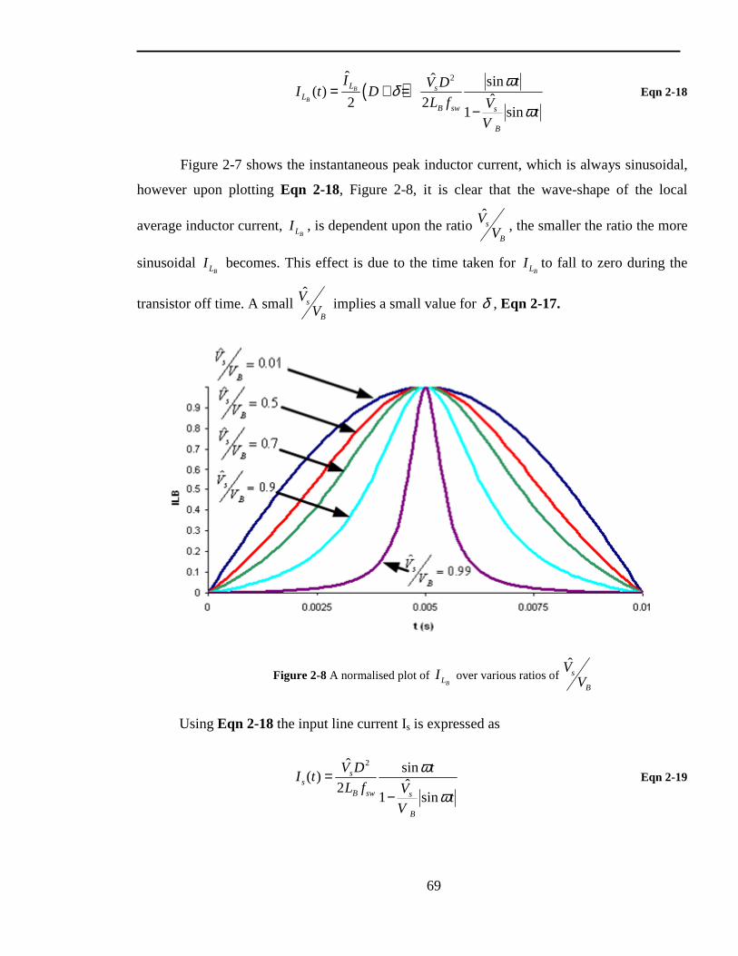
69
( )2ˆ ˆ sin
( ) ˆ2 21 sin
B
B
L sL
B sw s
B
I tV DI t D
L f Vt
V
ωδ
ω= + =
− Eqn 2-18
Figure 2-7 shows the instantaneous peak inductor current, which is always sinusoidal,
however upon plotting Eqn 2-18, Figure 2-8, it is clear that the wave-shape of the local
average inductor current, BLI , is dependent upon the ratio s
B
VV , the smaller the ratio the more
sinusoidal BLI becomes. This effect is due to the time taken for
BLI to fall to zero during the
transistor off time. A small sB
VV implies a small value for δ , Eqn 2-17.
Figure 2-8 A normalised plot of BLI over various ratios of s
B
VV
Using Eqn 2-18 the input line current Is is expressed as
2ˆ sin( )
ˆ21 sin
ss
B sw s
B
V D tI t
L f Vt
V
ω
ω=
− Eqn 2-19

70
As ( )sI t is not necessarily a sinusoidal waveform, using Eqn 2-19 the line rms current,
,s rmsI , over a line period is
[ ]2
, 0
1( )
lineT
s rms sline
I I t dtT
= ∫ Eqn 2-20
The instantaneous power, ( )inP t , over a complete line cycle is not constant, ( )inP t is
zero during the ( )sV t zero crossing, and maximum when sV is reached, Figure 1-7, and is
calculated by
( ) ( ) ( )in s sP t V t I t= Eqn 2-21
The average input power, inP , during a half line cycle can be derived
/ 2
0
1( ) ( )
/ 2lineT
in s sline
P V t I t dtT
= ∫ Eqn 2-22
As already detailed in Section 1.2.4 and Figure 1-7, the instantaneous load power, ( )oP t , is not
equal to the instantaneous input power,( )inP t , a capacitive storage component is required to
provide a low frequency energy storage element. Assuming a sinusoidal input, unity power
factor and a lossless converter, by equating the instantaneous input and output power under
steady-state converter operating conditions the capacitor voltage ripple from [126] is
expressed as
( ) 1 sin(2 )oB B
B B
PV t V t
C Vω
ω= − Eqn 2-23
where oP is the average output power, BC is the S4PFC boost capacitor.
Assuming that average input power, inP , of the S4PFC, is equal to the average output
power , oP , substituting Eqn 2-14 and Eqn 2-19 into Eqn 2-22 and rearranging for the duty
ratio, D, gives

71
/ 22
2
0
2sin ( )ˆˆ
1 sin( )
line
B sw o
T
s
s
B
L f PD
tV d t
Vt
V
πω ω
ω
=
−∫
Eqn 2-24
To ensure that the boost stage of the S4PFC stays in discontinuous current mode, then
Eqn 2-25 must be satisfied for all operating conditions.
1D δ+ < tω∀ Eqn 2-25
Assuming an ideal operation, using Eqn 2-23, the voltage transfer function of the
continuous conduction mode forward converter stage of the S4PFC can be expressed by
,( )o B p sV DV t N= Eqn 2-26
where ,p sN is the primary to secondary turns ratio of the transformer. Eqn 2-26 shows that
with a constant duty cycle, D, the twice line voltage ripple of ( )BV t will appear at the output
of the S4PFC, but may be attenuated by the Lo-Co output filter of the CCM forward stage,
depending upon the design values of the components.Various control approaches to reduce
this low frequency ripple voltage are detailed in [127, 128], however they both require
complex control strategies.
To limit the current ripple through the output capacitor, Co, and limit the overall
power losses of the forward converter stage, the output inductor, Lo, operates in continuous
conduction current mode for all operating conditions. Therefore, as opposed to Eqn 2-25, Eqn
2-27 must be true for all operating conditions.
1D + ∂ = tω∀ Eqn 2-27
where ∂ is the duty ratio for the falling current oLI until the the next switching cycle. The
output inductor, Lo, can be expressed as
ˆˆo
o
swo L
L
DTL V
I= Eqn 2-28

72
where oLV and
oLI are the peak voltage across and current through Lo.
2.1.3 Integrated Magnetic Principles of Operation
The transformer and the boost inductor are combined in the S4PFC topology, as seen in
Figure 2-1. The aim is to reduce the overall component count without a detrimental impact on
the performance. The approach taken is that the magnetic components should not interact, so
the magnetic flux produced by one will result in zero net effect on the operation of the other.
This section details the winding arrangement, the operation, and analysis of the integrated
magnetic. Figure 2-9 shows the IM core, its windings and the flux paths.
The boost inductor, LB, is split into two equal-turn windings, wound on the two outer
legs of the E-core. The coil former for the spilt inductor windings is bespoke. The flux
generated by the inductor, BLφ , plotted in red, flows in a clockwise direction around the outer
legs of the core. Any flux flowing through the centre leg due to BLφ cancels itself out, as they
have the same magnitude but opposite polarities, the result being that the centre limb can be
used for the forward converter transformer.
2BL
V
2BLN
BLi
1gl 2glpV pN
sV sN
rV rN
2Tφ
BLφ2Tφ
2BLN
2BL
V
Figure 2-9 Winding arrangement of integrated magnetic E-core
Figure 2-10 shows the wave shape of flux BLφ , which mirrors
BLI . As there is no
magnetic flux in the centre limb produced by the inductor windings, any windings wound
around the centre limb will not be coupled to LB.

73
BLφ
t0t 1t 2t 0 swt T+
Figure 2-10 Inductor generated flux, BLφ in outer legs
The transformer windings, Np, Ns, and Nr are wound around the centre leg of the E-
core, which does not require a custom manufactured core or coil former. The flux generated
by the transformer windings in Figure 2-9, Tφ , is drawn in green. Flux Tφ is generated in the
centre leg, divides equally, assuming the outer limb air gaps are the same, and flows in
opposite directions around the outer legs of the core. The magnitude and wave shape of Tφ in
the three legs of the core are drawn in Figure 2-11.
,T Lφ
,T Cφ
,T Rφ
t0t 1t 2t 0 swt T+3t
Figure 2-11 Transformer generated flux,Tφ , in all three core legs
As the two magnetic components are wound around the same core, the magnetic fluxes
Tφ and BLφ interact, resulting in a modification of the total flux level IMφ , Figure 2-12.
Assuming that the magnetic material is linear and applying the superposition theorem, the
instantaneous flux magnitude on the left leg of the core is determined by

74
, BIM L L Tφ φ φ= − Eqn 2-29
the instantaneous flux magnitude in the centre leg of the core is simply
,IM C Tφ φ= Eqn 2-30
and finally, the instantaneous flux magnitude in the right leg of the core is
, BIM L L Tφ φ φ= + Eqn 2-31
In this example, from Eqns 2-29 to Eqns 2-31 it can be seen that there is an imbalance
of flux levels. This results in a localised ‘hot spot’ of flux in the right leg of the magnetic core
leading to an increase of localised core losses and temperature. This is unavoidable, as any
other winding arrangement allows inductor flux to couple directly with the transformer
windings which may adversely affect the single-stage power factor corrector operation of the
converter. Alternative winding strategies are proposed in [99], which would ensure equal flux
magnitudes in each limb, but were considered overly complex and likely to have an
unacceptable cost penalty.
,IM Lφ
,IM Cφ
,IM Rφ
t0t 1t 2t 0 swt T+
Figure 2-12 Integrated magnetic component flux,IMφ , waveforms
To assist with the analysis, understanding and development of a SABER simulation
model of the integrated magnetic component, a gyro-capacitor model of Figure 2-9 is shown

75
in Figure 2-13. This modelling approach is introduced in Section 1.2.6, and is a method that
can express the non-linear effects and parasitics of a magnetic device whilst providing an
insight to the core’s operation [97-99]. For simplicity, flux leakage of the IM is neglected.
The magnetic core paths and permeances are represented by capacitors, where LC is
the left hand core limb, ,G LC is the left hand core gap, CC is the centre core limb, RC is the
right hand core limb and finally ,G RC is the right hand core gap.
,1BLN
BLI
,G LC
pI
,2BLV
,2BLN
,1BLV
,G RC
BLR
LCCC RC
pR
sI sR
rI rR
LI CI RI
,1LBN LR I,1LB BN LR I
rN
SN
PN
rN rR IrN CR I
sN sR I
sN CR I
pN pR I
pN CR I
PLV
sLV
rLV ,2LB BN LR I,2LBN LR I
Figure 2-13 Gyro-Capacitor model of integrated magnetic component
The IM windings BLN , pN , sN and rN are all represented by gyrators. The gyrator is
an ideal two-port circuit element that reflects the impedance at one port as its reciprocal at the
other, where R is the gyrator resistance of the respective winding, and a voltage source is
reflected as a current source.
The inductor winding BLN is split equally between the two outer core legs of the IM
and is represented by ,1BLR and
,2BLR respectively, with the inductor current BLI being identical
through both windings.

76
The transformer windings pN , sN and rN are modelled as gyrators pNR ,
sNR and
rNR respectively around the IM centre limb. The voltage sources of all the gyrators appear as
currents in the magnetic core path with the direction of current flow indicated.
2.2 S4PFC Prototype
This section details the design approach of the S4PFC based upon the analysis in
sections 2.1.2 & 2.1.3. An iterative and practical approach is followed to determine the
feasibility of the S4PFC with an IM component. Design variables such as maximum bus
voltage, VB, boost inductance, LB, and LP/LS/LR ratios are selected whilst IM design
approaches, converter power losses and cost analysis are considered. Steady-state SABER
simulations are performed on the S4PFC and the IM to verify the theoretical analysis.
2.2.1 Single-Stage Single Switch Power Factor Correction Specification
Table 2-1 details the specification of the power stage, which were set by the
sponsoring company PSU Designs. The S4PFC is designed to operate at a nominal 230 Vrms
input with an output voltage of 14 V at power of 180 W. The converter must also comply with
input current harmonic limitations for Class C equipment as shown in [13].
Table 2-1 S4PFC Converter with Integrated Magnetic Specification
Description Value Unit Input Voltage Vs 230
+10, -6% Vrms
Max Input Current Is 0.92 Arms
Output Voltage Vo 14 Vrms Output Voltage Ripple
oVɶ 100 mV
Output Current Io 12.8 A Peak to Peak Inductor Ripple
oLIɶ 3 A
Switching Frequency swf 100 kHz
Line Operating Frequency linef 50 Hz
Output Power Range Pout 90 - 180 W Converter Efficiency
PFCη 80 % @ 180 W
Power Factor PF ≥ 0.98

77
2.2.2 Design Procedure
To ensure that the S4PFC meets the specified input current harmonic regulations
detailed in section 2.2.1. The minimum ˆ /s BV V needs to be determined. The low frequency
input current harmonics are generated due to the trailing edge boost current in each switching
cycle. Assuming the line current Is averaged over a line period, is symmetrical, the complex
fourier coefficients of the input current shown in [129] are derived as
2
( )
0
1( )
2jn
s nI f e dπ
θθ θπ
−= ∫ Eqn 2-32
where n is the harmonic number. Substituting Eqn 2-19 into Eqn 2-32 and plotting over a
range of voltage ratios /s BV V using MATLAB Fast Fourier Transform simulator. The results
for the dominant odd harmonics with respect to the fundamental are shown in Figure 2-14.
The line connecting the cross symbols in Figure 2-14, indicates the harmonic limits
from the BS EN61000-3-2 standard Class C equipment [13]. The line marked with crosses
indicates the boundary for the European applications, min 216SV V= , and the one marked with
circles indicates the boundary for universal applications, minSV = 90 V. From this the minimum
permissible voltage ratios can be deduced, ˆ / 0.95s BV V < for European and / 0.83s BV V < for
Universal applications.
It can be seen that the largest input current harmonics occur for large voltage ratios of
ˆ /s BV V where the contribution of the trailing edge boost current, BLI , Figure 2-3, to the total
input current is the highest. All input current harmonics diminish as the boost voltage, VB,
increases compared to the peak line voltage, SV . The third harmonic is the most dominant
component, apart from the fundamental, well above 10 % for ˆ /s BV V ratios up to 0.43.

78
1 0.95 0.911
0.86 0.83 0
10
20
30
40
50
60
70
80
90
100
Ha
rmo
nics
as
pro
port
ion
of fu
ndam
enta
l, [%
]
ˆs
B
VV
Harmonic: 3rd 5th
7th 9th 11th 13th
Figure 2-14 Dominant input current harmonics for a range of voltage ratios
To limit the MOSFET conduction losses, a low-voltage device is preferred. This
however implies a low boost voltage and therefore a high distortion. Figure 2-14 is used to
identify the minimum /s BV V ratio for which the input current harmonic content complies with
Class C of [13].
Since the third harmonic, for practical voltage ratios ( ˆ / 0.91s BV V ≤ ), is much larger
than the other harmonics, compliance with the standard in reference [13] for the third
harmonic, usually guarantees fulfilment of the rest of the harmonics for this topology.
As well as determining the input current harmonics, the ratio ˆ /s BV V is required to
determine the converter input power factor. PF defined by [126] and is expressed as
in
P
PPF
S= Eqn 2-33
where Pin is the real power, and Sp is apparent power. Substituting Eqn 2-19 and Eqn 2-22
into Eqn 2-33 gives the form

79
, ,
in
s rms s rms
PPF
V I= Eqn 2-34
Figure 2-15 Power factor versus /s BV V
Plotting Eqn 2-34 over a wide range of /s BV V gives Figure 2-15. The BS EN 61000-3-
2 standard [13] does not specifically state a minimum power factor requirement. However, a
value of power factor is required in order to determine the maximum permissible third
harmonic current, expressed as a percentage of the fundamental, for Class C equipment. To
ensure low input current harmonics, a high power factor, whilst limiting peak semiconductor
current losses a /s BV V ratio of 0.7 is selected, giving a PF of approximately 0.98, and a third
harmonic 30 % of the fundamental frequency line current.
The boost stage inductor, BL , not only determines the peak switching current, ˆBLI , but
also peak magnetic core losses, power semiconductor conduction losses, the output boost
voltage, VB, and more critically the converter stage operating mode. Eqn 2-25 identifies the
condition that should be met in order for the PFC stage to remain in the DCM throughout the
entire line cycle. During a single switching cycle, see Figure 2-3 , the boost stage inductor, LB,
volt second balance is derived as
s sw s B swV DT V V Tδ= − Eqn 2-35

80
Using Eqn 2-14 and Eqn 2-35, Eqn 2-25 now becomes
( )ˆ sin
1 1 0ˆ sins
B s
V tD t
V V t
ω ω πω
+ ≤ ≤ ≤ −
Eqn 2-36
Eqn 2-36 shows that LB is most susceptible to entering the CCM at the peak of the line
voltage, sV . Using the MATLAB symbolic toolbox, the critical value of BL to maintain DCM
over half a line period is determined by substituting Eqn 2-24 into Eqn 2-36, giving
2
2
2
, 0
ˆˆ1 ˆ sin
ˆ21 sinˆ
ss
BB crit
o sw s
B
VV
V tL d t
P f Vt
V
π ω ωπ ω
−
=−
∫ Eqn 2-37
To determine the critical boost inductance, Figure 2-16 plots Eqn 2-37 with ˆ /s BV V
ratio of 0.7, an output power of 180 W and a switching frequency of 100 kHz, determined in
Table 2-1.
150
200
250
300
350
90 110 130 150 170 190 210 230 250 270
sV
,(
)B
crit
LHµ
Figure 2-16 ,B critL over the universal line input voltage range

81
In order to maintain DCM for all operating conditions ,B B critL L< . Figure 2-16 plots
Eqn 2-37 over a universal input voltage range with an output power of 180 W. Aware of the
limited winding space available on an integrated magnetic E-Core, the number of turns that
can be wound round the outer limbs and the packing factor, an inductance of 111 Hµ is
chosen for BL . This value of BL , guarantees that the converter PFC stage stays in DCM
despite not achieving the minimumBLI possible.
The instantaneous boost stage capacitor voltage,( )BV t , is given by Eqn 2-23. Plotting
this equation for various capacitances at output powers of 90 W & 180 W, the twice line ripple
frequency voltage BV∆ is shown in Figure 2-17. Decreasing the ˆ /s BV V ratio would reduce
BV∆ further, however the peak voltage stresses across components would increase.
0
20
40
60
80
100
120
0 20 40 60 80 100 120 140 160 180
( )BC Fµ
()
BV
V∆ 180oP W=
90oP W=
Figure 2-17 Boost capacitor stage low frequency voltage ripple at Po= 90 W & 180 W
Table 1-2 in section 1.2.7.4 summarises the performance and specification parameters
of a number of different capacitor types. Figure 2-17 shows that a capacitance of > 180
Fµ would provide the lowest BV∆ . Electrolytic capacitors can both adequately withstand high
voltages whilst providing sufficient capacitance for energy storage, however this capacitance
is not achievable at a BV of 570 V, unless specialised devices are used. Capacitors of the 350

82
V range are more readily available, therefore two 100 Fµ 350 V components in series are
used.
Since the CCM forward converter stage utilises the same MOSFET as the DCM boost
converter, the turns ratio of Np,s of the S4PFC are dictated by the values chosen for the ratio of
VB/Vo and the duty cycle, unlike a standard forward converter.
As the parameters such as duty ratio, D, and boost capacitor voltage, BV have already
been determined by the requirements of a high input power factor and low input current
harmonics, in order to realise the low output voltage, oV , listed in Table 2-1, then only the
primary-secondary turns ratio, ,p sN , of the IM can achieve this. Using the steady-state voltage
conversion ratio of a continuous conduction mode forward converter, ,p sN the required turns
ration is calculated as
,o
p sB
VN
DV= Eqn 2-38
At a nominal input line voltage and a maximum output power of 180 W, the duty ratio
D= 0.16 generates BV of 460 V, therefore using Eqn 2-38 the turns ratio of the S4PFC ,p sN is
0.19.
To limit the MOSFET peak voltage, QV during the transistor off-time, assuming that
the transformer reset time is equal to the transistor off-time, then the ratio of ,r pN is
calculated by
0
ˆr
p Q B
N V
N V V=
− Eqn 2-39
where rN and pN are the number of turns of the IM core reset and primary windings
respectively. Again using the converter operating parameters that have been already defined,
the reset-primary turns ratio ,r pN is 0.13. Determining the IM primary winding inductance,
pL , is an iterative process, as if too a low value is used PLI will become large, increasing the

83
primary conduction losses. Also if the number of turns in the windings is too low, the core
flux will be excessive, resulting in high core losses even saturation.
If pL is too large, then the total number of turns,pN , may not be accommodated by the IM
winding window. Efficient power MOSFETs that can withstand the converter parameters thus
far are detailed in section 2.3, and using Eqn 2-2 and Eqn 2-3, pL is defined as 1.1 mH . The
turns ratios defined in Eqn 2-38 and Eqn 2-39 define sL and rL as 41 Hµ and 20 Hµ
respectively.
To ensure that the forward converter stage of the S4PFC stays in continuous
conduction current mode for all operating conditions, the peak to peak current ripple of the
output inductor, oLIɶ , must be smaller than
oLIɶ defined in Table 2-1. The output inductor oL is
expressed as
4
o
D oo
L
V VL
I
−=
ɶ Eqn 2-40
Using Eqn 2-40, oL is chosen as 60 Hµ .
2.2.3 Design Summary
Table 2-2 lists a summary of the key component values derived in section 2.2.2.
Table 2-2 S4PFC key component values
Parameter Calculated Unit
BL 111 Hµ
pL 1100 Hµ
sL 41 Hµ
rL 20 Hµ
oL 60 Hµ
BC 50 Fµ
oC 1000 Fµ

84
Using the component values listed in Table 2-2, and the design approaches in section
2.1.2, Table 2-3 lists the key calculated values of the S4PFC with a nominal input voltage of
230 Vrms and an output power, Po of 180 W and 90 W.
Table 2-3 Key calculated values of S4PFC at a Pout of 180 W and 90 W
Pout= 180 W Pout= 90 W Parameter
Calculated Calculated
Unit
sV 230 230 Vrms
sI 1.37 0.59 A
linef 50 50 Hz
swf 100 100 kHz
D 0.16 0.13 -
δ 0.40 0.21 -
ˆBLI 4.8 3.8 A
QV 563 663 V
QI 7.9 5.7 A
BV 460 566 V
ˆpLI 3.15 1.92 A
oV 14 14 V
2.2.4 Integrated Magnetic Design
This section details the design procedure for selecting, gapping and winding the
integrated magnetic component. The principles of the integrated magnetic component
operation and winding arrangement are introduced in section 2.1.3, the aim of the IM is to
reduce the overall component count without having a detrimental impact on the performance
of the S4PFC. A winding approach is already proposed so that the magnetic components do
not interact, therefore the magnetic flux produced by one will result in zero net effect on the
operation of the other, Figure 2-12. Despite there being no magnetic coupling, the two
magnetic components are utilising the same core, and so the design procedure must be
complementary to ensure that the magnetic core can not only achieve the desired electrical
performance but also accommodate the total number of windings. Figure 2-19 shows a flow
chart detailing the iterative design process followed for the integrated magnetic component.

85
The first stage of the integrated magnetic design is the selection of a suitable core
material. Table 2-3 details the switching frequency of the S4PFC converter, a ferrite material
survey using [130], shows 3F3 to be the least lossy at this frequency range.
Selecting the E-Core size is an iterative process, as it is not yet known whether the
initially selected core will suffice until the design process in Figure 2-19 is completed. After a
number of iterations however the core size ETD 44 is selected. An ETD E-Core construction
was chosen due to the centre limb of the core being circular in cross section, therefore
increasing the winding area window and increasing the packing factor [130]. The maximum
allowable peak flux density, B , is determined from the magnetics ferrites core manual.
Due to the custom gapping arrangement used in the integrated magnetic, that is only
the outer limbs are gapped, the gap was calculated in the following way.
el
Figure 2-18 ETD core dimensions, not to scale
Using the physical core dimensions from Figure 2-18, the effective magnetic core path
length, el , the effective core volume, e
v , and the effective cross sectional areas, e
A of each of
the limbs are identified.

86
ˆBLB ˆ
PLB
ˆBLB ˆ
PLB
BLN pN
BLN , ,P S RN N N
BLN , ,P S RN N N
sN rN
pNBLN
Figure 2-19 Flow chart for the design of the integrated magnetic component

87
Using the physical dimensions of the selected core, the effective permeability of the
core, eµ is calculated as
1
ie
i
e
G
l
µµµ
=
+
Eqn 2-41
where iµ is the initial permeability of the core, [130], and G is the air gap length.
The inductance factor is determined by
( / )o e
LAI A
µ µ=Σ
Eqn 2-42
where 0µ is the permeability of free space, 74 10π −× Hm-1, and ( / )I AΣ is the core factor, a
ratio of the sum of the core limb lengths and cross sectional areas.
Using the required inductance values listed in Table 2-2, the total number of turns for
BLN , pN , sN and rN respectively is found using
L
LN
A= Eqn 2-43
Using Faraday’s law, the peak AC flux, Nφ , generated in a winding is
ˆ NN sw
VDT
Nφ = Eqn 2-44
where NV is the voltage across the winding. The total flux in each core limb is found using
Eqn 2-29 to Eqn 2-31 in section 2.1.3
The peak flux density in each core limb is
ˆˆ T
e
BA
φ= Eqn 2-45

88
where B , Tφ and eA , are the peak flux density, peak flux and core cross sectional area
respectively of that particular limb.
From Figure 2-17, if the peak flux density in the right hand core limb, RB , exceeds the
already established maximum peak flux density of the core, then either increase the core air
gap length or increase the core size. If ˆRB is within limits, the windings
BLN , pN , sN and rN
can now be calculated. Selecting the current density, J , for each winding, the total cross
sectional area of wire, cuA , is
rmscu
IA
J= Eqn 2-46
where rmsI is the respective RMS current of that particular winding. The skin depth, SK, of the
current in each of the windings is calculated as
66( )
sw
SK mmf
= [131] Eqn 2-47
Due to the skin and proximity effects, multiple parallel wire strands are used to
minimise the AC resistance of the winding.
Should ,cu totalA , shown in Eqn 2-48, be less than the total core winding area available
then the core may be wound, if not, then the winding current densities, J , must be increased.
, ncu total n cun
A p N A= ∑ Eqn 2-48
where , , ,BL p s rn N N N N= and p is the packing factor which includes winding build up and
insulation.
The DC wire resistance of each winding is determined by
cudc
cu
lR
Aρ= Eqn 2-49

89
where ρ is the resistivity of copper, and is 61.724 10 cm−× Ω at 20 C° .
The AC wire resistance of each winding is determined by
58.32 10 swac
fR
SK
−×= Eqn 2-50
Table 2-4 lists the IM component parameters, including the magnetic core details, the
number of turns required for each winding, the peak flux generated in each winding and
finally the main integrated magnetic loss components.
Table 2-4 Integrated magnetic core parameters and operating values at 180 W
Parameter Unit Core manufacturer Ferroxcube - Core type ETD 44 - Core material 3F3 - Effective volume 17800 mm3
Effective length 86 mm Effective area 174 mm2
Max flux density 350 mT Initial permeability 1740 - Effective permeability 50 - CC CL,R Core factor 0.589 0.164 mm-1 Mean turn length 77 56 mm
LB L p L s L r Inductance 111 1100 41 20 µH
Number of turns 32 101 20 14 - Flux 20 7.8 - µWeb Flux density 111 40 - mT Wire length 2.77 7.8 1.51 1.05 m Current density 3.00 3.00 3.00 3.00 A/mm2
Wire diameter 0.82 0.68 1.42 1.03 mm2
Skin depth 0.20 0.20 0.20 0.20 mm DC Wire resistance 0.24 0.25 0.12 0.16 Ω AC Wire resistance 0.35 0.95 0.91 0.33 Ω Copper loss @ 100 C 1.46 1.42 3.76 1.41 W Core loss @ 100 C 0.51 0.05 - W Total losses @ 100 C 8.57 W

90
Numerous transformer winding arrangements were investigated, but the winding
arrangement seen in Figure 2-20 was found to minimise leakage between the transformer
windings Np, Ns and Nr, and minimise losses due to winding proximity effects.
The primary winding, Np, is divided in two and sandwiched between windings Ns and
Nr. This results in a transformer winding arrangement, of a layer of ½ Np, a layer of Nr, the
second layer of ½ Np and finally a layer of windings of Ns. This transformer winding
arrangement also allows for the effective cooling of Ns as it is the most lossy winding in the
IM device due to the high current of the output of the converter. The boost inductor windings
BLN are a single layer of turns around the two outer legs of the core.
sN
rN/2pN
/2pN
/2BN
Figure 2-20 Cross section of transformer winding arrangement
The final magnetic prototype incorporating all of the windings is shown in Figure 2-21.
It can be seen that all of the window area available for winding is used and is the main limiting
factor for this IM design. A higher value of LB would be ideal to reduce the ˆBLI , but with this
core, the window area is insufficient.

91
Figure 2-21 Integrated magnetic prototype
2.3 Component Selection and Loss Audit
MOSFET devices are the natural choice for this low power high frequency application.
Assuming that the voltage and current waveforms at the switching instants of the MOSFETs
are linear, an approximation of MOSFET losses was made using the procedure set out in
Appendix A. A number of suitable MOSFETs for Q were identified and listed in Table 2-5.
Despite MOSFET FQP3N80 being the cheapest, its switching losses are the highest. To strike
a balance between cost and efficiency STW10NK80 was chosen. The costs of all components
in this section are single piece quotes at 2009 prices.
Table 2-5 Selection of suitable Si MOSFETs for Q
Component Voltage Rating
(V)
Continuous Current
(A)
Rdson
Norm (Ω)
Tr
(ns) Power Loss (W)
Device Cost (£)
STW10NK80 800 9 1.6 27 8.62 2.55 FQP3N80 800 3 4.0 40 26.5 0.31
STP8NK80 800 6 1.75 14 13.6 2.96 SPA11N80C3 800 11 0.7 37 1.57 3.77
Despite silicon carbide diodes, discussed in section 1.2.7.1, having very low switching
losses, they are expensive, therefore all of the diodes shortlisted in Table 2-6 to Table 2-9 are
silicon devices. Table 2-6 is a shortlist of suitable diodes for D1. Again, assuming that the
voltage and current waveforms at the switching instants of the diode are linear, an
approximation of diode losses was made using the procedure set out in Appendix B. Diode

92
BYV-29 has the lowest estimated losses, however the cost is more than twice that of diode
SF36 whose combined conduction and switching losses are comparable, therefore the SF36 is
the preferred device for D1.
Table 2-6 Selection of suitable Si diodes for D1
Diode Rated Voltage
(V)
Rated Current
(A)
Trr
(ns)
Forward Voltage
(V)
Power Loss (W)
Cost (£)
UF5408 1000 3 75 1.70 1.8 0.30 SF36 400 3 35 1.30 1.4 0.52
FEP14GT 400 16 50 1.30 1.5 0.90 BYV-29 400 9 60 1.03 1.1 1.7
Table 2-7 is a list of a number of diodes appropriate for D2. As the current 2DI is
discontinuous, the switching losses are significantly lower. Diode FEP16GT has the lowest
estimated losses. Diode UF5408 is the least expensive device but has the highest losses. SF38
is the preferred device based upon cost despite having similar estimated losses as 31DF6.
Table 2-7 Selection of suitable Si diodes for D2
Diode Rated Voltage
(V)
Rated Current
(A)
Trr
(ns)
Forward Voltage
(V)
Power Loss (W)
Cost (£)
UF5408 1000 3 75 1.70 2.2 0.30 SF38 600 3 35 1.70 2.0 0.52
FEP16GT 600 16 50 1.50 1.6 0.90 31DF6 600 3 35 1.70 2.4 0.86
A common cathodes dual diode package was chosen for D3 and D4 to reduce the
overall component count. The candidate components are listed in Table 2-8, of those listed the
BYW51-200 is selected due to the lowest power loss and relative cost.

93
Table 2-8 Selection of suitable Si diodes for D3 and D4
Power Loss (W)
Diode Rated Voltage
(V)
Rated Current
(A)
Trr
(ns)
Forward Voltage
(V) D3 D4
Cost (£)
BYW51-200 200 10 25 0.85 4.0 8.0 0.60 DSA-20 100 10 40 0.80 3.8 7.5 0.69
ON-BMRF20
100 10 30 0.85 4.1 8.0 1.28
The possible components for the transformer reset diode, D5, are seen in Table 2-9.
Due to the low forward voltage drop and low piece cost, the diode UF5401 is the most suitable
device in this case.
Table 2-9 Selection of suitable Si diodes for D5
Diode Rated Voltage
(V)
Rated Current
(A)
Trr
(ns)
Forward Voltage
(V)
Power Loss (W)
Cost (£)
UF4004 400 1 75 1.7 4.0 0.09 UF5401 100 3 50 1.0 2.5 0.41
HERG302 100 3 50 1.0 2.5 0.57 ES3B100 100 3 30 0.62 1.5 0.69
Table 2-10 lists a number of suitable electrolytic capacitors for CB. To achieve the
necessary capacitance and voltage stresses, yet be capable of withstanding the ripple current,
two 350 V capacitors need to be arranged in series. For each of these devices, calculations in
Appendix C show that capacitor EEUE2E101 generates the lowest losses and is relatively
inexpensive.

94
Table 2-10 Selection of suitable electrolytic capacitors for CB
Capacitor Rated Capacitance
( )uF
Rating Voltage
( )V
I rms
( )mA
tanδ Power Loss (W)
Cost (£)
EEUE2E101 100 350 2100 0.15 0.03 1.53 107LBB400-
M2 100 350 1700 0.15 0.02 2.97
EEUE2V101 100 350 1600 0.20 0.03 0.57 TF10118-
X25 100 350 2160 0.15 0.02 1.78
Suitable output capacitors for Co are detailed in Table 2-11. Due to converter output
voltage ripple requirements, these capacitors are electrolytic devices. As Vo is relatively low,
there is no requirement to series this component, therefore capacitor EKZE250ELL is
selected.
Table 2-11 Selection of suitable electrolytic capacitors for Co
Capacitor Rated Capacitance
( )uF
Rating Voltage
( )V
I rms
( )mA
tanδ Power Loss (W)
Cost (£)
108KXM025 1000 25 2360 0.14 0.004 0.77 EKZE250-
ELL 1000 25 2360 0.14 0.004 0.43
25YXF1000 1000 25 2360 0.14 0.004 0.67 25ZKL1000 1000 25 2250 0.16 0.005 0.90
For the selected devices Figure 2-22 shows a breakdown of the estimated power losses
in the S4PFC operating at a worst case condition of Vs= 216 Vrms, a maximum duty ratio of 20
% and a Pout= 180 W. Parasitic losses in the input filter, input rectifying diodes, PCB tracking,
input/ output connectors and control circuitry are ignored and not included in this analysis.
The components used were not only selected due to their electrical characteristics but also due
to their cost and availability, to ensure that the overall system costs were comparable to those
of a two-stage PFC/regulator approach.

95
0.0
1.0
2.0
3.0
4.0
5.0
6.0
7.0
8.0
9.0
10.0
Q D1 D2 D3 D4 D5 CB Co IM Lo
Component
Po
wer
(W
)
Core
Switching
Conduction
Figure 2-22 Estimated power losses in S4PFC power devices.
The MOSFET, STW10NK80, exhibits the largest single loss of all the power devices
in the S4PFC, with 5 W of conduction loss and 3.6 W of switching losses. The MOSFET
SPA11N80C would have produced a total loss of 1.57 W, but the cost is significantly higher.
Diodes D1 and D2 are UF5408 and have comparable losses of 1.87 W and 2.18 W. The
conduction losses are the dominating loss contributor, and could be significantly reduced by
using SiC diodes, but again like the MOSFET would impact the overall cost of the S4PFC.
The forward converter stage rectifying diodes D3 and D4 are a single package device
consisting of two diodes, BYW51-200. This package is carefully heat-sinked, as the combined
power losses of the two diodes are the largest single heat source in the converter. Like D1 and
D2, the diodes have little switching losses.

96
Table 2-12 A summary of the expected losses detailed in Figure 2-22
Device Component Loss (W) Q STW10NK80 8.62 D1 SF36 1.87 D2 SF38 2.18 D3 BYW51-200 4.06 D4 BYW51-200 8.02 D5 UF4004 4.03 CB EEUE2E101 0.02 Co EKZE250ELL 0.004 IM - 8.57 L0 - 3.58
Total 40.95 Efficiency 81.4%
If the more efficient devices were used the estimated power loss of the S4PFC would
be 27.4 W with a system efficiency of 87 %. However the relative component cost increase
would be 55 %, which would have made the converter uncompetitive for the target
application.
2.4 Steady-State SABER Simulation
A SABER model was designed to confirm the predicted results detailed in Table 2-3.
Figure 2-23 shows an idealised model of the S4PFC with an IM component, a simple control
block provides the duty cycle pulses to achieve the necessary output voltage. A differential
mode filter and line-frequency rectifier is included for completeness.
The converter was modelled by assuming all the power stage components are ideal
devices, the MOSFET is modelled as an ideal switch with zero on-state resistance and infinite
off-state resistance. The power diodes are piece wise linear components with zero forward volt
drop. The output capacitors are also ideal with no parasitic resistance or inductance. The
integrated magnetic, comprising the boost inductor and the forward converter transformer is
modelled discretely. The core legs are modelled by their respective inductance factors, AL,
derived from the core dimensions detailed in [130] and respective air gaps, section 2.2.4. The
magnetic core material is ideal, with no hysteresis losses. The IM windings, are lossless, with
no parasitic resistance, interwinding capacitance or leakage inductance.

97
Figure 2-23 SABER schematic capture of S4PFC with IM
The following simulation results demonstrate the steady-state performance of the
S4PFC for Vo= 14 V, LB= 111 µH, Lp= 1.1 mH, Ls= 41 µH, Lr= 20 µH, Lo= 60 µH, CB= 50
µF, Co= 1000 µF and swf = 100 kHz.
Figure 2-24 shows a number of key simulated waveforms for the S4PFC operating over
a number of switching frequency cycles at an input voltage Vs= 230 Vrms and an output power
Pout= 180 W. All waveforms are captured at sV .These ideal simulated waveforms closely
correspond to the theoretical waveforms seen in Figure 2-3, and to the calculated results as
seen in Table 2-3. Despite using an integrated magnetic component, the winding arrangement
of the two magnetic components does not impact upon the performance of the S4PFC.

98
Figure 2-24 Key SABER simulated waveforms, Vs=230 Vrms, Po=180 W
Figure 2-25 details simulation results demonstrating the steady state performance of
the S4PFC, again, for an input voltage Vs= 230 Vrms and Vo= 14 V, however the output power
is Pout= 90 W. All other component values are as before. Once again, the steady state
measurements from SABER simulations correspond closely with calculated results, as shown
in Table 2-13.

99
Figure 2-25 Key SABER simulated waveforms, Vs=230 Vrms, Po=90 W
Figure 2-26 shows plots of sV , sI , BV and Vo over a number of line cycles with a
power output of 180 W. As the boost stage of the S4PFC is operating in DCM, sI is
proportional and in phase with sV , indicating a near unity power factor and low harmonic
current content. The input current, sI , is not purely sinusoidal however, this is due to the non-
linear operation of the DCM boost converter. The twice mains frequency voltage ripple can be
clearly seen in the trace of BV . The amplitude of the AC ripple decreases with reduced load,
but the DC level of BV increases with the lighter load. The output voltage, Vo, has a small AC
ripple component, due to the twice mains frequency ripple of BV .

100
Figure 2-26 SABER simulated waveforms of Vs, Is, VB, and Vo at Po=180 W
Figure 2-27 SABER simulated waveforms of Vs, Is, VB, and Vo at Po=90 W
Figure 2-27 shows plots of sV , sI , BV and Vo over a number of line cycles with a
power output of 90 W. With a reduced load of 50 % of the nominal, the boost stage output
voltage, BV , increases as expected with DCM operation, but the voltage ripple decreases from
30 V to 12 V. The output voltage ripple, oVɶ , also reduces in amplitude to 38 mV.
Table 2-13 lists a comparison of calculated results in section 2.2.3 and simulated
results of the S4PFC. As expected it shows a close correlation between the two and reinforces

101
the validity of the calculations. Any disparities are due to simulation sampling rates,
algorithms employed by the simulator and approximations in the analysis.
Table 2-13 Comparison of key calculated and simulated results
Pout= 180 W Pout= 90 W Parameter
Calculated Simulated Calculated Simulated
Unit
sV 230 230 230 230 Vrms
sI 1.37 1.49 0.59 0.69 A
linef 50 50 50 50 Hz
swf 100 100 100 100 kHz
D 0.16 0.17 0.13 0.14 -
ˆBLI 4.8 5.1 3.8 4.1 A
QV 563 566 663 669 V
QI 7.9 8.1 5.7 5.9 A
BV 460 458 566 569 V
ˆpLV 460 457 566 560 V
ˆpLI 3.15 3.07 1.92 1.80 A
oV 14 14.04 14 14.04 V
Figure 2-28 shows simulated and calculated input current harmonics and compares
them with respect to the allowable harmonic limits at an operating power of 180 W. The
calculated results are accurate for the dominant harmonics, namely the 3rd, 5th and 7th, with
noticeable errors for the low line conditions. The even harmonics are too small to be
considered and are deemed negligible.
As expected the worst case input current harmonics occur at low line due to the higher
peak currents generated by the DCM boost inductor. These results verify Figure 2-14 that a
s
B
VV ratio of 0.7 would limit input harmonic currents sufficiently to satisfy allowable limits.

102
0
0.1
0.2
0.3
0.4
0.5
0.6
0.7
0.8
3 5 7 9
Harmonic
Cu
rren
t (A
)
Harmonic Limits
Simulated Harmonics
Calculated Harmonics
(a)
0
0.1
0.2
0.3
0.4
0.5
0.6
0.7
0.8
3 5 7 9
Harmonic
Cu
rren
t (A
)
Harmonic Limits
Simulated Harmonics
Calculated Harmonics
(b)
Figure 2-28 Simulated and calculated input current harmonics (a) sV = 265 Vrms and (b)
sV = 216 Vrms
Figure 2-29 plots the flux in each of the legs of the SABER simulated integrated
magnetic seen in Figure 2-23. Due to the winding arrangement of the split boost inductor, NB,
and the transformer windings, Np, Ns, Nr, there is an increased flux level in the right leg of the
core, CR, compared to the left core leg, CL, which will result in added core losses in this leg.

103
This effect can be overcome by increasing the number of turns of 1BLN and reducing
2BLN but
this will destroy the core symmetry.
Figure 2-29 SABER simulation of integrated magnetic flux waveforms
2.5 Summary
This chapter presents a theoretical study, analysis and design of a single-stage, single-
switch power factor corrector, S4PFC, with an integrated magnetic component.
The steady-state analysis of the S4PFC with an integrated magnetic component goes
beyond any current work presented for this topology. Modes of converter operation are
detailed and expected waveforms drawn. Design equations such as for sB
VV ratio to determine
the dominant input current harmonics, and the maximum duty cycle are realised, with an
understanding of the design trade offs such as cost, complexity and performance. Integrated
magnetic analysis, design calculations/ process and winding approaches are realised that
enable the amalgamation of two magnetic components onto a single core yet avoid electrical
interaction.
MATLAB and SABER simulations verify the predicted steady-state performance of
the S4PFC as well as characterising the IM component. These results allowed for optimisation

104
of the power stage and provided results for the most suitable components to be selected for a
prototype S4PFC.
Part of this work formed a conference paper and poster presentation at the IEEE Power
Electronics and Drives Systems Conference, November 2005, in Malaysia.

105
3 Single-Stage Single-Switch PFC Converter Dynamic Behaviour and Control Design
3.1 Introduction
This chapter details the dynamic behaviour of the S4PFC with an IM and its control
requirements. Small-signal models of the S4PFC converter are realised and the requirements of
a control loop discussed. A suitable control approach is identified from Chapter 1, along with
an analysis of the characteristics of the controller. Using MATLAB Control Toolbox, the line-
to-output, control-to-output and compensator transfer functions are realised and modelled.
Design of the compensator is performed and a practical control approach that provides
galvanic isolation is designed and modelled. A mixed-signal switching SABER model of the
power stage and control loop is conducted that validates the predicted operation, stability and
performance of the loop.
3.2 Line-to-Output
The S4PFC converter analysed in Chapter 2 is a cascaded boost converter operating in
DCM and a forward converter operating in CCM, Figure 3-1. Neglecting the input EMC filter,
the line-to-output transfer function for a DCM boost converter [126] is shown in Eqn 3-1.
sV
Figure 3-1 Single-stage single switch power factor corrector with simple control block

106
ˆ 0
ˆ( )
ˆ 1s
B Bv
s d
p
v GG s
svω
=
= =+
Eqn 3-1
where the ^ symbol over a lower case variable denotes a small perturbation around the steady-
state operating point and
sB
B
VG M
V= = Eqn 3-2
and
22
(1 )p pB B
Mf
M R Cω π−= =
− Eqn 3-3
where RB is the effective boost stage load resistance defined by 2
BB
o
VR P= and CB is
the boost stage capacitance. The line-to-output transfer function of Eqn 3-1 exhibits a single
pole at pω .
Assuming the turns ratio of the forward converter Np,s = 1:1, the line-to-output transfer
function for a CCM forward converter from [126] is
2ˆ 0
20 0 0
ˆ 1( )
ˆ1
( )
B
ov
B d
vG s D
v s s
Q ω ω=
=
+ +
Eqn 3-4
where D is the duty ratio, 1
o
o oL Cω = and Qo is defined by
0o o
o o esr o
L CQ
L R R C=
+ Eqn 3-5
where Lo is the forward converter output filter inductor, Co is the output capacitance, Ro is the
output load resistance and Resr is the Equivalent Series Resistance, ESR, of Co. The line-to-
output transfer function of Eqn 3-4 exhibits a double pole atoω and a resonant peak of oQ .

107
Therefore the total line-to-output transfer function of the single-stage, single-switch power
factor corrector is realised by Eqn 3-6
( ) ( )s Bv v vG s G G s= Eqn 3-6
Figure 3-2 Magnitude and Phase plot of Gv(s) at sV = 230 V and oP = 90 W and 180 W
Using the MATLAB Control Toolbox, Figure 3-2 is a plot of Eqn 3-6 with the S4PFC
converter component values listed in Table 2-2 at sV = 230 V and an output power of 90 W
and 180 W. At oP = 90 W the magnitude plot shows the low frequency pole of the
discontinuous boost converter, pf at 2.3 Hz, the -20 dB/dec slope above 2.3 Hz and the
associated -90 phase shift. The high frequency complex pole, of , due to the continuous
forward converter stage is at 650 Hz, and an additional – 180 phase shift is added to the
response. Above 650 Hz the magnitude plot shows a role off -60 dB/dec slope.
At oP = 180 W, the high frequency complex pole, of , does not change, apart from an
increase in gain magnitude. However the low frequency pole of the discontinuous boost
converter, pf , increases to 8 Hz.

108
3.3 Control-to-Output
The control-to-output transfer function of the S4PFC converter is that of a conventional
CCM forward converter shown in Eqn 3-7 [126].
2
20 0 0
1
( )
1( )
zBvd
s
VG s
N s s
Q
ω
ω ω
+
=
+ +
Eqn 3-7
where 1o
o oL Cω = and 1
zo esrC Rω = . Inserting the S4PFC component parameters from
Table 2-2 into Eqn 3-7 , Figure 3-3 shows a plot of the control-to-output of the S4PFC using
MATLAB, traced in orange at sV = 230 V and a maximum power output of 180 W. The
resonant pole, of is at 650 Hz with a –40 dB/dec magnitude roll-off above this frequency. The
high frequency zero, zf , due to the parastic ESR of Co is at 650 kHz. Reducing oP to 90 W,
does not change the frequency position of of or zf , only increasing the resonant peak oQ .
Figure 3-3 SABER and MATLAB plots of control-to-output of the S4PFC

109
Figure 3-3 clearly shows that the small-signal behaviour of the DCM boost stage of the
S4PFC has no impact upon the performance of the control-to-ouput of the converter
Using the SABER simulation model shown in Figure 3-4, the results of a time domain
system analyser, TDSA, is plotted on the same axis as the MATLAB simulation results in
Figure 3-3. The two plots show a close correlation between the simulation approaches, any
disparities that are seen is due to the sampling rate of the SABER simulation approach. The
parameters for the TDSA are listed in Table 3-1. By increasing max_nper and increasing the
quality factor of the input band pass filter the accuracy of the SABER plot can be improved at
the expense of computational time and memory. The simulation time required to provide the
results for Figure 3-3, took an average of 4 hours and 6 GB of memory.
Figure 3-4 SABER simulator arrangement to determine S4PFC ( )vdG s

110
Table 3-1 Control parameters for the TDSA component in SABER simulations
Name Value
fbegin 50
fend 100000
ampl 0.1
Offset 0
npoints 100
Mode logswp
Max_err 0.01
Max_nper 30
Min_nper 3
Min_tspp 40
ao 1
qo 10
Filter Yes
ac mag = 1, phase = 0
3.4 Identification of Suitable Control Approach the S4PFC
This section identifies a suitable control approach from section 1.2.5 which reviews
power factor correction control methods for CCM and DCM converters.
As the boost stage of the S4PFC operates in discontinuous current mode, the control
loop is not required to perform power factor correction, only output voltage regulation.
Therefore, commonly implemented current mode approaches such as average and peak
control, are not necessary unless a current or power limiting function is required. The simplest
approach is a single-loop voltage-mode control, Figure 3-5, where ( )cG s , ( )pwmG s , ( )vdG s ,
and ( )dKG s are the transfer functions of the compensator, the PWM modulator, the S4PFC
control-to-output and the feedback attenuator respectively.

111
ˆovˆrefv( )vdG s( )pwmG s( )cG s
( )dKG s
dˆcv
ˆdKv
Figure 3-5 Single loop voltage mode control
The closed loop equation of the single-input, single-output control loop in Figure 3-5 is
expressed as
( )1
vd c
vd c d
G GH s
G G K=
+ Eqn 3-8
Closed loop stability of a linear system is achieved if all the roots of its characteristic
equation, 1 0vd c dG G K+ = , has negative real parts [132], that is, the roots are to the left of the
imaginary axis in Figure 3-6. To achieve closed loop stability and a fast transient response, a
suitable control compensator cG is required.
Im
Re
Stable
RegionUnstable
Region
0
Figure 3-6 Stability regions in the complex plane for roots of the characteristic equation

112
The control-to-output transfer function, vdG , plotted in Figure 3-3, shows the gain
magnitude exhibiting a second-order response at pf and a phase shift tending towards -180 .
To ensure system stability and fast transient response, a PID control, Eqn 3-9, is required to
perform loop compensation [126]. This control approach can obtain both a wide frequency
bandwidth and a zero steady-state error.
1 2
1 2
1 1
( )
1 1
gz z
c
p p
s s
G ss s
s
ωω ω
ω ω
+ +
=
+ +
Eqn 3-9
The compensator ( )cG s exhibits the following characteristics, the zero at 1z
ω adds low
frequency gain. The second zero at 2z
ω adds phase lead at the vicinity of the loop gain
crossover frequency, cf . Combined, 1z
ω and 2z
ω can provide a phase boost upto 180 . The
poles at 1pω and
2pω provide high frequency roll off to attenuate the high frequency switching
ripple interfering with the pulse width modulator. Finally, gω is the gain of the compensator at
cf . Figure 3-7 shows the S4PFC with a simplified block diagram of the voltage mode
feedback loop.
sV
refv( )pwmG s ( )cG s ( )
dKG s
ˆov
d
ˆcv ˆdKv
Figure 3-7 S4PFC with a block diagram of the proposed voltage mode control loop

113
To ensure that galvanic isolation is maintained, an isolation stage is required in the
feedback loop. A common approach is detailed in [133] and shown in Figure 3-8, this circuit
consists of the feedback attenuator network, Kd, an error amplifier, ( )eaG s , an optocoupler,
( )ocG s and a PWM modulator with gate drive, ( )pwmG s .
( )pwmG s
d
dK
( )eaG s
pC
LR
431TL
1R
2R
( )vdG s
1C
2C
3RcR
AV
ˆcv
ˆov
( )ocG s
Figure 3-8 Practical implementation of isolated feed back and compensation
The attenuation resistor network, Kd, comprising the resistor network 1R and 2R ,
reduces Vo to 2.5 V which is the internal precision voltage reference of the TL431 [134]. The
TL431 comprises of a stable internal 2.5 V reference which is connected to an internal
operational amplifier inverting input. The operation amplifier output drives an internal open
collector transistor. In this approach, the TL431 is used as the error amplifier of the
compensator and eliminates the need for an auxiliary power supply for the error amplifier
network. The output of the TL431 is powered through the resistor RL and the optocoupler
signal diode, connected in series with the output voltage, Vo. The TL431 error amplifier now
operates as a transconductance amplifier, therefore ( )cG s comprises ( )eaG s and ( )ocG s . By
generating the compensation error signal, cv , on the primary side, as opposed to transferring a
proportional signal of the output voltage to the primary side, the impact of the optocoupler’s

114
non-linearity and high gain variation is minimised. The optocoupler error signal, cv , is
compared with a set/reset latch in block, ( )pwmG s , where duty cycle, D, is generated.
For the practical control approach in Figure 3-8, the subsequent position of the zeros
and poles of Eqn 3-9 are determined by Eqn 3-10 to Eqn 3-14 [135].
1
1
1z
cR Cω = Eqn 3-10
The second zero position 2z
ω is realised by
2
3 2
1( )z
LR R Cω =
+ Eqn 3-11
The first pole position 1pω is expressed by
1
3 2
1p R C
ω = Eqn 3-12
The second pole position 2pω is expressed by
2
1p
c cR Cω = Eqn 3-13
Finally gω is realised by
cg
L
RCTR
Rω = Eqn 3-14
where CTR is the current transfer ratio of the opto-coupler.
3.5 Design of Control Loop
To achieve a fast transient response whilst maintaining loop stability, the overall open
loop gain, ( )olG s , should have a unity gain cross over frequency, cf , approximately 1/5th
below the switching frequency, swf , with a slope of -20 dB/dec and the corresponding phase

115
margin at the unity cross-over should be approximately 45 - 70 to ensure a satisfactory
damping ratio. The overall open-loop transfer function, ( )olG s , is expressed as
( ) ( )dol vd c pwm KG s G G G G s= Eqn 3-15
Figure 3-8 shows the practical implantation of the feedback attenuator, ( )dKG s ,
comprising of resistors 1R and 2R . To ensure that the TL431 reference input is sufficiently
biased, the current through 1R , 1RI , should be greater than biasI over the entire temperature
range [134]. The attenuator network is derived by Eqn 3-16 and Eqn 3-17.
2
2ref
R
VR
I= Eqn 3-16
where refV is the internal reference of the TL431, and 2 1R R biasI I I= − .
1
1o ref
R
V VR
I
−= Eqn 3-17
From Eqn 3-16 and Eqn 3-17 arbitrarily choosing 1RI to be 1 mA, then 1R = 11.5 kΩ
and 2R = 2.5 kΩ , therefore ( )dKG s is 0.17.
To ensure a stable switching frequency, swf , a pulse width modulator and efficient
MOSFET gate drive, a UC2842 control IC is used [136]. Figure 3-9 shows a block diagram of
the UC2842, detailing its functionality.
The S4PFC switching frequency is set by the UC2842 internal oscillator and by the
addition external components TR and TC and is derived by Eqn 3-18 [136].
1.72sw
T T
fR C
= Eqn 3-18
The MOSFET gate driver is realised by an internal totem pole arrangement. The PWM
is determined by a set-reset latch, therefore ( )pwmG s = 1. The control IC also provides a

116
regulated 5 V reference, AV . As the loop compensator, ( )cG s , is defined by the approach
shown in Figure 3-8, the UC2842 internal operational amplifier is redundant along with the
internal voltage reference. The output voltage, cv , of the compensator ( )cG s is fed directly
into Pin 1 of the UC2842.
AV
Figure 3-9 Block diagram of UC2842 control IC
Before the design of ( )cG s can take place, the transfer function, ( )oG s must be
characterised and is expressed as
( ) ( )do vd pwm KG s G G G s= Eqn 3-19
Figure 3-10 shows a plot of Eqn 3-19 and that at a required overall open loop transfer
function, at the target frequency cross over, cf , of 10 kHz, the gain magnitude is -25 dB with
a phase shift, PS, of – 178 . Therefore to achieve an overall open-loop transfer function,
( )olG s , of unity gain crossover at cf and a phase margin, PM, of 65 , the compensator, ( )cG s ,
must provide a gain at cf of 25 dB and a phase boost, PB, of 152 .

117
Figure 3-10 Plot of ( )oG s
The phase boost, PB delivered by( )cG s is defined as
90PB PM PS= − − Eqn 3-20
Placing the zeros, 1z
ω and 2z
ω of Eqn 3-9 at 3455 rads-1, and 1pω and
2pω at 3.5x10⁶
rads-1, to attenuate any high frequency switching noise, results in the compensator( )cG s plot in
Figure 3-11. At the target cf , 10 kHz, the gain magnitude is 25 dB with a phase boost totalling
152 .
Using Eqn 3-10 to Eqn 3-14, the practical component values of Figure 3-8 to achieve
the ( )cG s plot in Figure 3-11, are 1R = 11.5 kΩ and 2R = 2.5 kΩ , 3R =54 Ω , LR =5.6 kΩ ,
pR = 20 kΩ , 1C =25nF , 2C = 50 nF and pC = 145 pF .

118
Figure 3-11 MATLAB plot of ( )cG s
The resulting open-loop gain ( )olG s is plotted in Figure 3-12. It can be seen that there
is a unity gain cross over at 1/5th of the swf with a –20 dB slope. The phase margin at cf is
65 as expected.
Figure 3-12 MATLAB plot of ( )olG s

119
Figure 3-13 shows a normalised step response of the transfer function H(s) in Eqn 3-8
It confirms that the loop is stable with a response typical of a system with a phase margin of
65 , settling within 2 ms of the disturbance.
Figure 3-13 A normalised step response of closed loop system H(s)
3.6 SABER and MATLAB Simulation Verification
The results of the MATLAB control analysis in section 3.5 are verified with SABER
mixed signal switching simulations. Figure 3-14 shows the SABER model of the control
system ( )dK s , refv , ( )cG s , and ( )pwmG s . The control loop is simulated along side the S4PFC
SABER switching model in Figure 2-23.
The following SABER simulations demonstrate the dynamic performance of the
S4PFC converter and the proposed control approach. The results presented are all for a
nominal input voltage Vs = 230 Vrms with the output power, Pout, stepping from 180 W to 90 W
back to 180 W.

120
Figure 3-14 SABER simulation schematic of control loop for S4PFC converter
Figure 3-15 shows the response of the S4PFC with a step load change of 180 W to
90 W, where sV , sI , BV and oV are plotted. At time 0.14 s to 0.2 s the output power is 180 W,
the input current, sI , is in phase with the input voltage, Vs, indicating a high power factor. sI
is not purely sinusoidal, as it is distorted by the non-linear performance of the DCM boost
converter. At time 0.2 s, a step load change occurs from 180 W to 90 W. The input current, sI ,
remains in phase with sV but reduces in amplitude, whilst the control loop of Figure 3-14,
maintains the regulation of oV . As BV is not regulated there is an increase in this voltage from
460 V to 560 V. The amplitude of the ripple content of oV also reduces with the reduced load.

121
Figure 3-15 SABER simulation of Vs, Is, VB, and Vo in response to a step load change of 180 W - 90 W
at t = 0.2 s
Figure 3-16 is a magnified image of Figure 3-15 now plotting Vo and oI . At time
0.1992 s to 0.2 s the load is 180 W, the output voltage is closely regulated to 14 V and the
output current is 12.8 A. At time 0.2 s, a step down in load to 90 W occurs. The output voltage
responds by rising to 14.29 V at time 0.2001 s. The response of ( )cG s overcompensates
causing Vo to undershoot at 0.2005 s, however by time 0.201 s, Vo has settled to the steady-
state value, exhibiting a classic second order response.
Figure 3-16 Magnified view of SABER simulation Io and Vo response to step load of 180 W to 90W

122
Figure 3-17 SABER simulation of Vs, Is, VB, and Vo in response to a step load of 90 W to 180 W at t =
0.4 s
Figure 3-17 shows the response of the S4PFC to a step load change where sV , sI , BV
and oV are plotted. At time 0.36 s to 0.4 s the output power is 90 W, the input current, sI , is in
phase with the input voltage, Vs, again indicating a high power factor. At time 0.4 s, a step
load change occurs from 90 W to 180 W. The input current, sI , remains in phase with sV but
increases in amplitude, whilst the control loop, Figure 3-14, maintains regulation of oV . As BV
is not regulated there is a decrease in this voltage from 560 V to 460 V. The amplitude of the
ripple in oV also increases with the increased load.
Figure 3-18 is a magnified image of Figure 3-17 showing Vo and oI . At time 0.3992 s
to 0.4 s the load is 90 W, the output voltage is closely regulated to 14 V and the output current
is 6.4 A. At time 0.4 s, the load steps to 180 W. The output voltage responds by dropping to
13.75 V at time 0.4001 s. The response of ( )cG s overcompensates causing Vo to overshoot at
0.4005 s, however by time 0.4018 s, Vo has settled to the steady-state value.

123
Figure 3-18 Magnified view of SABER simulation Io and Vo response to step load 90 W to 180 W
From these simulations it can be seen that the simulated model of the power stage and
its control loop are performing as expected. Neither step up or step down load changes appear
to cause any sub harmonic instabilities.
3.7 Summary
This chapter details the dynamic performance and the requirements of the S4PFC
converter control loop. The dynamic analysis of the S4PFC with an IM has not been found in
any of the literature reviewed by the author. The converter line-to-output and control-to-output
transfer functions, suitable control approaches are realised, as well as the necessary circuit
protection measures to ensure there is no over voltage of the DCM boost stage capacitors
under light load conditions.
A suitable control approach is identified from Chapter 1, and evaluated using
MATLAB and SABER simulations, designed and implemented, ensuring a fast transient
response to step load changes, whilst ensuring loop stability. A practical approach is
developed that allows for fast dynamic response, but also provides the required galvanic
isolation between the primary and secondary.
The MATLAB and SABER switching model simulations confirm the theoretical
results increasing the confidence in the S4PFC small-signal analysis and validate the identified
control approach.

124
4 Experimental Performance of S4PFC with IM
4.1 Introduction
Following the analysis and design of the S4PFC with an IM device in Chapters 2 and 3,
this Chapter details the development of the prototype converter. Firstly, the construction and
layout approach used is shown along with the experimental laboratory set-up. Secondly,
verification of the operation of the S4PFC with an IM device is performed, comparing SABER
simulations and experimental waveforms, validating the design. Finally, a cost analysis is
discussed.
4.2 Circuit Construction and Experimental Setup
This section details the experimental laboratory setup, including the design and layout
of the Printed Circuit Boards, PCBs, the equipment used for verifying the performance of the
single-stage, single-switch power factor corrector. The PFC stage and the respective control
components are arranged so that they occupy a small area to minimise parasitic inductance
loops. The power stage and the control loop are closely arranged on a single board. The PCB
is FR4 insulating fibre glass with a single sided 1oz copper layer. Full schematic drawings of
the S4PFC circuit diagram can be found in Appendix D.
Figure 4-1 PCB capture of S4PFC layout and tracking

125
Figure 4-1 shows the circuit layout for the S4PFC converter. The input line connection,
Vs, is on the bottom left hand side of the power board. This input is fused for safety and
voltage surge suppression components are also added. Immediately following the fused input
are the EMC components, X-capacitors C103, C104 and a common-mode inductor, L100. The
network of components in the upper left corner of Figure 4-1 is the UC2842 PWM controller
and supporting devices. The main switching power MOSFET, Q, is labelled Q100 in this
diagram. The main boost capacitors are located in the centre of the board and are labelled
C107 and C110. The integrated magnetic component is clearly seen as it is the largest single
device on the PCB and is labelled IM100. L200 is the output filter inductor of the forward
converter stage. Use of space was minimised to ensure compactness and efficiency. There are
also numerous test points situated across the circuit board for ease of testing. The dimensions
of the converter in Figure 4-2 is 250 mm x 150 mm x 100 mm.
Figure 4-2 S4PFC with integrated magnetic prototype
Once the PCB had been populated, detailed testing was undertaken using a artificially
generated single phase AC sine voltage to ensure a good distortion free voltage waveform, a
Integrated Magnetic
Input Filter & Rectifier
Boost Capacitors
Output Inductor
Output
Control
D1 & D2
MOSFET D3,4 & D5

126
Yokogawa WT3000 power analyser recorded and assessed the line voltage and current
waveform quality and harmonic content, and a Lecroy WaveRunner oscilloscope along with a
high voltage differential probe ADP305 and a AP105 current probe was used to measure
converter waveforms. Figure 4-3 shows the laboratory set up used to evaluate the S4PFC
prototype.
Figure 4-3 Laboratory setup
4.3 Experimental Verification and Performance Comparisons
The following sections detail the measured steady-state waveforms of the prototype
S4PFC and compare them with the theoretical predictions and SABER simulations over a
number of operating conditions. Input current quality and harmonics are plotted at various line
and loads states, as well as comparisons of key converter waveforms.

127
4.3.1 Input Current Quality and Harmonic Content
Figure 4-4 and Figure 4-5 show experimental and simulated results of the S4PFC line
supply voltage, sV , and supply current, sI , to determine wave shape quality, power factor and
current harmonic content. The SABER simulations presented in this section are the result of
mixed signal modelling of the steady-state S4PFC schematic in Figure 2-23 with the
component values listed in Table 2-2, and the control loop shown in Figure 3-14.
The simulated results are plotted in solid black lines, whilst the corresponding
experimental results are plotted in colour. Figure 4-4 compares experimental and simulated sV
and sI , where sV = 230 Vrms and the converter output power is 180 W. The plots show
comparable current waveforms. Despite the input current, sI , not being purely sinusoidal due
to the non-linearity of the DCM boost stage, it is in phase with sV , indicating a high power
factor and low harmonic current content.
Figure 4-4 Simulated and experimental waveforms of sI and sV where sV = 230 Vrms and P0 =180 W
The amplitude of the experimental sI results is larger than that of the simulated sI
results due to the S4PFC parasitics and resistive losses that are not included in the SABER
simulations. The small phase shift between the experimental results and the simulated results
is due to slightly different line frequencies, the simulated frequency is accurately set to 50 Hz,
however, in practice this is not precisely matched.

128
Figure 4-5 Simulated and experimental waveforms of sI and sV where sV = 230 Vrms and P0 =90 W
Figure 4-5 plots simulated and experimental results of sI and sV at an output power of
90 W. sI is again in phase with sV and there is a closer correspondence with the simulation
data.
Table 4-1 S4PFC input measurements over various operating conditions
Vs (V)
I s (A)
Ps (W)
Po (W)
S (VA)
Q (VAR)
ϕ ( )
PF (%)
Vs THD (%)
I s THD (%)
260 0.44 114 90 79 21 10.8 98 0.200 2.8 230 0.50 115 90 78 20 10.0 98 0.217 2.7 215 0.54 116 90 77 19 9.6 98 0.215 2.8 260 0.60 156 120 76 11 4.1 99 0.187 4.0 230 0.69 158 120 75 9 3.3 99 0.176 5.4 215 0.77 165 120 72 10 3.5 99 0.178 6.2 260 0.92 239 180 75 12 2.9 99 0.169 7.1 230 1.05 241 180 75 12 2.8 99 0.166 7.5 215 1.13 242 180 74 11 2.8 99 0.168 7.9
Using a Yokogawa WT3000 power analyser, Table 4-1 lists the experimental results of
the input voltage and current quality at various operating conditions of th S4PFC. Where S is
apparent power, Q is reactive power, ϕ is the phase angle between sV , and sI . Power factor
is labelled as PF and THD is the total harmonic distortion of sV and sI respectively. Since ϕ

129
is small across the operating conditions listed in Table 4-1, the subsequent power factor is near
unity as expected with a boost converter operating in DCM, resulting in a low apparent power
and successive reactive losses.
4.4 Steady State Waveforms
Figure 4-6 to Figure 4-8 show simulated and measured steady state waveforms of the
S4PFC with an output power of 180 W and an input line voltage of 230 Vrms. All of the
simulations were performed with ideal components at a switching frequency of 100 kHz. The
SABER simulated results are plotted in solid black lines, whilst the corresponding
experimental results are plotted again in colour. Figure 4-6 plots waveforms of the
discontinuous boost inductor current, BLI , and corresponding
BLV . The experimental
waveforms show close correlation with the simulated results in terms of wave shape and
magnitude. The phase shift seen between the simulated and experimental results is due to
slightly different switching frequencies and formatting discrepancies, the simulated frequency
is accurately set to 100 kHz, however in practice the experimental switching frequency is 101
kHz, due to component tolerances. This applies to all figures in this section comparing
simulated and experimental results.
Figure 4-6 Simulated and experimental waveforms ofBLI and
BLV for sV = 230 V and P0 =180 W
The higher peak current BLI in the experimental result is attributed to PCB circuit
losses, resistive winding losses and other parasitics not included in the simulation. These

130
parasitic effects also have an impact upon the duty ratio of the experimental results as the
control loop automatically increases the duty ratio to compensate for the circuit losses and
maintain the output voltage at the required level.
Despite efforts to ensure a compact and efficient circuit layout, track inductance and
parasitic semiconductor capacitances also cause resonant ringing of the boost inductor voltage
during the discontinuous current stage of the waveforms. This parasitic oscillation is
especially evident in Figure 4-8 and Figure 4-11 and invariably adds to converter power
losses. A small overshoot is also evident in the QV waveform at the turn-off instant which was
attributed to the layout inductance and the leakage inductance of the transformer.
Figure 4-7 Simulated and experimental waveforms ofQI and QV for sV = 230 V and P0 =180 W
The results in Figure 4-7 show that the experimental and simulated waveforms closely
agree, however once again, unaccounted for component parasitics cause leading edge parasitic
ringing in the experimental results. The experimental waveform of voltage QV is slightly
lower than the simulated result due to a number of reasons. Higher than expected resistive and
parasitic losses increase the load on the output of the boost stage, further, with BV being lower
than predicted, the duty ratio, D, must increase in order to achieve output voltage, oV ,
regulation. The result of increasing D consequently reduces the time period 3t to 0 swt T+ in
Figure 2-3, pushing this recovery stage close the CCM as seen in the lack of step in the
experimental wavform QV in Figure 4-7.

131
Figure 4-8 shows plots of simulated and experimental waveforms of 1DI and
1DV at an
output power of 180 W. The two waveforms of 1DI show close correclation, yet the
experimental 1DV shows significant high frequency ringing at the reverse bias voltage
transition and low frequency ringing when BLI becomes discontinuous due to a less than ideal
component layout, contributing to converter losses. The near continuous conduction mode
operation of the transformer reset winding is also apparent in the experimental waveform of
1DV as seen in the lack of step in Figure 4-8.
Figure 4-8 Simulated and experimental waveforms of1DI and
1DV for sV = 230 V and P0 =180 W
Figure 4-9 Simulated and experimental waveforms ofBLI and
BLV for sV = 230 V and P0 =90 W

132
Figure 4-9 to Figure 4-11 shows steady state plots of the S4PFC at an output power of
90 W. Again like the converter operation at 180 W the experimental results at 90 W shows
close correlation to the simulated plots especially the experimental current plots of BLI , QI ,
1DI and 2DI , for all of the conditions shown, confirming the expected performance and design
of the integrated magnetic.
Figure 4-10 Simulated and experimental waveforms of QI and QV for sV = 230 V and P0 =90 W
Figure 4-11 Simulated and experimental waveforms of2DI and
2DV for sV = 230 V and P0 =90 W
Considering magnetic core utilisation, the analysis assumes that there is better core
usage of the integrated magnetic approach compared to using separate magnetics. This

133
assumption is based upon the total core volumes involved in each case. Yet in practice, the
desired core cannot always accommodate the total number of windings required, making it
difficult to realise appreciable volume savings. Non-ideal elements in the converter still
dominate during periods (1-D)Tsw causing unwanted oscillations.
In conclusion to this section, the comparisons between the experimental results and the
ideal SABER simulation results validate thoroughly the steady-state analysis and design
performed in earlier sections, with the integrated magnetic performing as expected.
4.5 Cost Analysis
A cost evaluation of the S4PFC is conducted in order to determine whether this single-
stage single switch with an integrated magnetic approach is financially viable compared to the
standard two-stage approach. In order to simplify the cost analysis and comparison of the two
approaches, the S4PFC and the two-stage prototypes are based on the same specifications.
Table 4-2 outlines the critical component analysis of the PFCs. The first column is the
standard two-stage converter approach, the second details the S4PFC with separate magnetic
components. Finally, the third column shows again a S4PFC, however this now utilizes
integrated magnetics. All figures are normalized for simplicity, and the standard two-stage
rectifier converter is used as a cost reference. The value of ‘3’ for the IM is with reference to
the combined cost of the boost inductor and the transformer in the two-stage converter.
Table 4-2 further shows the evident cost increase of having to utilize a high voltage
and current rating for the MOSFET, 2.75. The technology used for this device is a relatively
new introduction to the commercial market and its cost therefore will fall with time.
Again, like the MOSFET, high rated parts that can withstand the voltage imposed and
current ripple tend to be more costly components. So, in the S4PFC two boost capacitors are
arranged in series to withstand the stresses imposed, resulting in the high cost for this
component.
The IM assembly is more expensive than that of the conventional separate magnetic
components. This is again due to the technology being immature, therefore there is a high cost
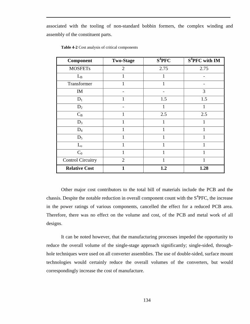
134
associated with the tooling of non-standard bobbin formers, the complex winding and
assembly of the constituent parts.
Table 4-2 Cost analysis of critical components
Other major cost contributors to the total bill of materials include the PCB and the
chassis. Despite the notable reduction in overall component count with the S4PFC, the increase
in the power ratings of various components, cancelled the effect for a reduced PCB area.
Therefore, there was no effect on the volume and cost, of the PCB and metal work of all
designs.
It can be noted however, that the manufacturing processes impeded the opportunity to
reduce the overall volume of the single-stage approach significantly; single-sided, through-
hole techniques were used on all converter assemblies. The use of double-sided, surface mount
technologies would certainly reduce the overall volumes of the converters, but would
correspondingly increase the cost of manufacture.
Component Two-Stage S4PFC S4PFC with IM
MOSFETs 2 2.75 2.75
LB 1 1 -
Transformer 1 1 -
IM - - 3
D1 1 1.5 1.5
D2 - 1 1
CB 1 2.5 2.5
D3 1 1 1
D4 1 1 1
D5 1 1 1
Lo 1 1 1
C0 1 1 1
Control Circuitry 2 1 1
Relative Cost 1 1.2 1.28

135
Further associated cost savings with the single-stage PFC that are not detailed in Table
4-2, include the costs of tracking, storing and assembling 26% fewer components than the
two-stage Converter, this is mostly due to the elimination of a control loop.
This very small cost saving, compared to the high percentage savings from component
reduction, is due to the manufacturing stage in which these components are inserted. Variable
Centre Distance, VCD, and Axial Insert, AI, equipment was used to place all of these
components automatically. Therefore, the impact of a reduction in assembly time/cost is
minimal.
4.6 Summary
This chapter has described the development of the experimental prototype S4PFC with
an IM device. The detailed experimental results presented for the S4PFC circuit show excellent
correlation with earlier theoretical predictions and simulations, showing that this approach
exhibits a near unity power factor with input current harmonics falling within specified limits,
whilst being able to provide a regulated output voltage. An important contribution is
demonstrating that this IM arrangement can be implemented within the S4PFC topology,
reducing component count and increasing core usage, whilst having little detrimental affect
upon the performance of the power stage.

136
5 Ultra Bright White Light Emitting Diode Driver
5.1 Introduction
This chapter details the design and development of a power converter for a high power
white light emitting diode street luminaire. A suitable power topology is identified for the
power factor correction stage and the constant current regulator stage, and necessary
modifications are made in order to fulfil the requirements specified in Chapter 1. The steady-
state operation of the converter is detailed, as well as the essential design equations. MATLAB
and SABER simulations characterise the steady-state performance of the converter and verify
the design equations. Finally, simulated and experimental results verify the design methods
and validate the approach for a HP LED street luminaire.The street light is to be used on main
distributors, and is of lighting class M3a. Main distributors are routes between strategic
highways such as dual carriage ways and urban centres, where speed limits are < 40 mph
[123].
These issues impact on the design of the HP LED street light, leading to an unusual
electrical design. Taking into account these concerns, Figure 5-1 shows the design of the
concept luminaire which will adhere to the regulations, and includes both the power converter
and HP LED strings.
Figure 5-1 CAD drawing of proposed LED Street Light

137
5.2 HP LED Power Converter Requirements
As already detailed in Chapter 1, HP LEDs cannot be directly connected to the mains
supply, as firstly they require reverse voltage protection, secondly, the current through the HP
LEDs needs to be regulated, and finally there are harmonic limits specified for lighting
equipment that is connected to the mains grid. The power factor correction stage limits line
harmonic currents, minimises total harmonic distortion, and provides sufficient energy storage
during the twice per cycle voltage zeros. A secondary converter is required to regulate the
current through the HP LED strings.
An added difficulty is the elimination of any electrolytic capacitors, so that a long
converter lifetime can be achieved, see section 1.2.7.2. as the useful operational lifetime of HP
LEDs is 50,000 hours. Many commercially available PFC drivers implement the lowest cost
electrolytic capacitors available for the requirement, to minimise 100 Hz ripple frequency and
perform energy storage. Yet these electrolytic capacitors have an operating lifetime of
typically several thousand hours [40]. If exposed to high temperature environments or high
ripple currents, the lifetime of these wet electrolytic capacitors will be reduced further due to
the electrolyte evaporating and venting and so the operating life of the entire system would be
compromised. In order to provide continuous power flow to the load and avoid 100 Hz
stroboscopic effects, a capacitor with the necessary energy storage capacity is needed. This
can be realised by using a long life, > 50,000 hours, electrolytic capacitor, which is expensive
and too large to fit in the luminaire, or using a non-electrolytic capacitor operating at a high
voltage to provide the necessary energy storage.
Metal film capacitors are suitable for high voltage use and have long lifetimes. These
capacitors are inexpensive and physically small [137] compared to long life time electrolytic
capacitors [43]. Other characteristics include low ESR, low ESL, low dissipation factor and
high reliability. These attributes all indicate that this capacitor type would be suitable for this
application. Metal film polyester dielectric construction is preferred over a film/foil
construction due to the self healing properties, smaller relative size and lower cost per
microfarad, see Figure 5-2.

138
Figure 5-2 Metallised film capacitor construction
Assuming metal film capacitors are used, the only PFC converter options are those
topologies that can boost the output voltage higher than the peak line voltage.
As well as being electrically efficient, durable and requiring low maintenance during
its lifetime, the power converter must also meet street luminaire optical standards which
govern the quality of the light output [42, 123, 138] and section 1.2.8. Of particular concern
are stroboscopic effects.
To avoid these unwanted effects a secondary cascaded converter is required to produce
a constant current in the LEDs. This converter must operate at switching frequencies beyond
the sampling frequencies of camera equipment and human visual perception. The converter
also performs a light dimming function if required.
Figure 5-3 is a block diagram of the HP LED power converter arrangement. The power
factor block contains the input EMC filter, mains rectifier, energy storage, and auxiliary power
supplies. The other three blocks are controlled constant current regulators which each supply a
HP LED string. These regulators are independent of one another, as this approach allows for
control of the street luminaires optical footprint.

139
sV
sI busV
V0
Figure 5-3 HP LED power converter block diagram
5.3 Power Factor Correction Converter Selection
Since the HP LED street light will draw more than 25 W of power from the supply, it
is subject to Class C requirements of British Standard 61000-3-2:2006 [13]. This class is more
stringent than other classes, as it is the only case where a limit for the 2nd harmonic input
current is specified, see Table 1-1.
Referring to Figure 5-3, the capacitor, C, must store enough energy to allow it to
supply the LED drivers during the twice per cycle mains voltage zeros, so that the voltage
supplied to these never falls below the minimum necessary for correct operation.
This requirement precludes passive PFC approaches and the active buck switching
converter topology identified in Chapter 1, since the DC link voltage must be higher than the
peak line voltage, sV . Section 1.2.3 describes the power imbalance that the active PFC stage
must compensate, and using Eqn 5-1, the output voltage, busV , of the PFC, must be higher
than sV .
2,
sin(2 )obus C mean
P tV E
ωω
= ± Eqn 5-1
Therefore the remaining suitable converters are boost and buck-boost type converters.
An isolated topology such as the flyback converter is not required, as galvanic isolation adds
complexity to the power stage. Other converters identified for PFC include the Cuk, Sepic and

140
Zeta converters. The operation of these converters, Section 1.2.3, reveal that they do not have
an inherent PFC ability, produce a distorted input current waveform and are not suitable for
this application.
The author believes the buck-boost converter is the most suitable power topology for
the role of street luminaire PFC. The converter is able to boost its output voltage to a level
significantly higher than its input voltage, albeit this is a negative voltage. The negative
voltage is not problematic for this application, as the load comprises constant current
regulators and HP LED strings. The converter can be operated in DCM, which automatically
shapes the input current to be directly proportional to the input voltage, ensuring a near unity
power factor and a simpler approach to control than continuous current mode operation. This
is beneficial since lighting harmonic current regulations are more stringent than for other
equipment.
5.4 Principles of Operation of Power Factor Correction Stage
This section details the discontinuous operation of the power factor correction buck-
boost converter, Figure 5-4. As this power stage offers no significant research interest, only
brief principles of operation of the power stage are given along with simulations and a power
loss audit of the regulator.
1QI1DI
1Q
busV
busI
1L
1D
1C
1LI
busRrecVsV
sI
Figure 5-4 Buck-boost power factor corrector stage

141
Described is the state-by-state operation and key waveforms, see Figure 5-6. This
section also details the analysis and predicted performance of the power factor correction
circuit. With the buck-boost converter operating in DCM, the topology can eliminate the need
for unnecessary complex control circuitry and requires only a small 1L value compared to a
CCM inductor. Control circuit simplification is achieved due to the inherent operation of the
DCM. The current through 1L becomes zero at some time within the off-period of Q1, in each
switching cycle, thereby ensuring the peak value of input current is proportional to voltage and
in phase with it, resulting in a near resistive input impedance for the stage. With this
approach, a high PF can be realised. Along with Figure 5-6, a description of the operating
principles of a DCM buck-boost restifier is given.
1QI
1CI1Q
busV
busI
1L
1D
1C1LI
busRrecVsV
sI
1LV
Figure 5-5 Buck-boost converter at t0 to t1
During period nTsw to tn1, the effective circuit of the buck-boost converter is shown in
Figure 5-5. MOSFET Q1 is conducting and the input voltage Vrec is applied to inductor L1. The
current through L1 and Q1 is given by
1
1
ˆˆsL
sw
VI
DT L= Eqn 5-2
where D and Tsw are the duty cycle and switching period of the buck boost power stage
respectively.

142
t(s)
1QV
1LI
1CI
1DV
swnT 1nt ( 1) swn T+
recV
busV
1
^
LI
busV
recbus VV +
recbus VV +
recV
0
0
0
0
0
0
0
1LV
1QI
1DI
2nt
,s nt,r nt
Figure 5-6 Key waveforms of DCM buck-boost converter

143
Diode D1 is reversed biased and capacitor C1 supplies the current to the output load.
Thus
1
^
1
s sw
L
V DTI
L= Eqn 5-3
The reverse bias voltage across diode D1 is given by
1D rec busV V V= + Eqn 5-4
During the time, tn1 to tn2, Q1 is off and the circuit is shown in Figure 5-7. The inductor
is connected to the output load and capacitor via D1 and the energy stored in L1 transfers to C1
and the output load. Q1 voltage becomes
1Q rec busV V V= + Eqn 5-5
The voltage across L1 is now equal to Vbus.
1DI
1Q
busI
1L
1D
1C
1LI
busRrecVsVsI
1LV
1CI
busV
Figure 5-7 Buck boost converter during t1 to t2
In discontinuous current mode control, 1LI falls to zero before the start of the next
switching cycle. This period 1nt to 2nt is given by

144
1
^
1,
L rec swr n
bus bus
I L V DTt
V V
⋅= = Eqn 5-6
During the remaining off period tn2 to (n+1)Tsw the inductor current 1LI is zero. This
time period is determined as
2( 1) ssw n sw sw sw
bus
V Dn T t T DT T
V
+ − = +
Eqn 5-7
The output capacitor C1 now supplies current to the load during this period.
1Q
busI
1L
1D
1CbusRrecVsV
sI
busV
Figure 5-8 Buck boost converter during period 2nt to ( 1) swn T+
The high frequency output voltage ripple swbusVɶ is
( )1
^
, 11
Lbus sw n sw
IV t nT
C= −ɶ
Eqn 5-8
Thus far, the analysis of the buck-boost converter has only been concerned with the
steady-state DCM condition over a single switching cycle. Neglecting the effect of an input
filter, over a single line period the input voltage, sV , is time varying as described by

145
ˆ( ) sins sV t V tω= Eqn 5-9
where sV is the peak line voltage, ω , is the angular frequency of the line voltage. Similarly
the rectified voltage, recV , is defined as
ˆ( ) sinrec sV t V tω= Eqn 5-10
With a constant duty cycle, over half a line period, the DCM buck-boost inductor
current is similar to that of the DCM boost current of the S4PFC shown in Figure 2-7.
However, unlike the DCM boost converter the trailing edge of 1LI is not seen by the input, as
shown in Figure 5-9.
t
sV
gV πω
swnT ( 1) swn T+
sI
ˆsI
0
Figure 5-9 Buck boost input voltage, sV , and current, sI , over a half line period.
From Eqn 5-3 and Eqn 5-9, the peak inductor current, 1LI can be defined as
1
1
ˆ sinˆ s
L sw
V tI DT
L
ω= Eqn 5-11
From Figure 5-6, the average current of 1LI during swnT and ( 1) swn T+ can be found as

146
1
1
,,
ˆ
2s n L
L nsw
t II
T= Eqn 5-12
Substituting Eqn 5-4, Eqn 5-6 and Eqn 5-11 into Eqn 5-12 yields
1
2
,1
ˆ sin2
swL n s n
bus
D TI V t
LVω= Eqn 5-13
Therefore the average current of inductor L1 over a half line period of 0 to /π ω is
described as
1
2 22
01 1
ˆ ˆsin
2 4s sw s sw
Lbus bus
D V T D V TI t dt
LV LV
πωω ω
π
= =
∫ Eqn 5-14
Assuming no converter losses, thus in oP P= , from Eqn 5-13
2 2
1 1
ˆ ˆ
4 4s sw s bus
bus bus sw bus
D V T D V V
LV LV f R= = Eqn 5-15
From [139] the voltage gain is defined as
1
ˆ
2s
bus
L
DVV
τ= Eqn 5-16
where 1
1 swL
bus
L f
Rτ = is the normalised inductor time constant.
To ensure that the converter remains in discontinous current mode, Eqn 5-17
determines the boundary conduction conditions.
ˆ 2(1 )bus
BC
s
V DM
DV= =
− Eqn 5-17
Figure 5-10 plots the duty cycle against the converter voltage gain of Eqn 5-17

147
BCM
Figure 5-10 Boundary conduction of buck boost PFC coverter
Therefore to maintain discontinuous current mode the inequality of Eqn 5-18 must be
satisfied.
11bus
Lsw
RL
fτ< Eqn 5-18
As C1 will be a metal film capacitor of a few Fµ value, so the voltage across it, Vbus,
will have a high component of ripple at 100 Hz as seen in Figure 5-11. The RMS current of C1
is
1, 1,
2 2
rms rms rmsC D busI I I= − Eqn 5-19

148
t (s)
busVbusVɶ
0
10msV ,maxbusV
,minbusV
Figure 5-11 Vbus waveform
The 100 Hz ripple voltage can be determined by
,min ,maxbus bus busV V V= −ɶ Eqn 5-20
where
2,min
12o
bus busline
PV V
f Cπ
= −
Eqn 5-21
and
2,max
12o
bus busline
PV V
f Cπ
= +
Eqn 5-22
linef and oP are the line frequency and the output power of the PFC converter respectively.
Note, that from Eqn 5-20, busVɶ , varies with load current, this result is of interest when
determining the control parameters, see Chapter 6.
5.5 Buck Boost Power Factor Correction Specification
Table 5-1 details the specification of the power stage, which were set by the
sponsoring company Dialight Lumidrives. The HP LED PFC is designed to operate at a
nominal 230 Vrms input with an output power of 180 W. The converter must also comply with
input current harmonic limitations for Class D equipment as shown in [13].

149
Table 5-1 HP LED power factor corrector specification
Description Value Unit Input Voltage Vs 230
+10, -6% Vrms
Max Input Current Is 1.0 Arms
Line Operating Frequency linef 50 Hz
Output Power Range Pout 60 - 180 W Converter Efficiency
PFCη 80 % @ 180 W
Power Factor PF ≥ 0.98
5.6 Converter Optimisation and Component Selection
In order to achieve maximum performance of this power converter stage whilst
obtaining long operating lifetime and converter reliability, parameters such as the switching
frequency and peak component voltage stresses need to be identified. The design approach
becomes an iterative process, as not only does the most optimal electrical performance need to
be chosen but also the component cost and physical size needs to be evaluated and a balance
found. This section details the design and selection of the key electrical power components
discussing the balance to achieve maximum converter performance whilst minimising size and
cost. Before the optimisation process can begin a number of parameters are defined. The
operating phase voltage range is 230 Vrms +10 % -6 %, the output bus voltage of the PFC stage
is -600 V, this value was arbitrarily chosen to ensure a high PF, provide sufficient energy
storage due to the low buck-boost capacitance, and to obtain an efficient duty ratio for the
current regulator stage. The output power range of the stage is 60-180 W. Therefore from Eqn
2-17 the voltage ratio M, varies between 1.60 and 1.96.
Using the normalised inductor time constant, 1Lτ and inserting various values for L1, a
value of 900 Hµ ensures that the buck-boost PFC converter stays in discontinous current
mode over all line and load conditions.
Figure 5-12 plots 1Lτ over low and high line, low and high output power loads showing
the operating area of the PFC power stage. The plot clearly shows the converter operating in
DCM with sufficient margin as to ensure no CCM boundary cross over.

150
Figure 5-12 DCM buck boost PFC operating area.
As the minimum value of L1 to maintain DCM has been identified, peak and average
currents can be determined and consequently semiconductor and capacitor devices can be
shortlisted.
Table 5-2 lists a number of suitable switching power MOSFETS for Q1. These devices
are all rated to withstand the peak voltage, as determined by Eqn 5-5, and are inexpensive and
readily available.
Table 5-2 Selection of suitable Si MOSFETs for Q1
Component Voltage Rating
(V)
Continuous Current
(A)
Rdson
Norm (Ω)
trr
(ns)
Device Cost (£)
Toshiba 2SK1120 1000 8 1.75 50 5.07 Toshiba 2SK1119 1000 4 1.9 18 3.79 ST STP5NB100 1000 5 1.75 11 4.90
ST STP8NK100Z 1000 6.3 1.75 19 3.23 IR IRFBG50 1000 6.1 1.6 35 8.79 IR IRFBG30 1000 3.1 2.0 25 1.66
Vishay IRFPG40 1000 4.3 1.75 33 3.51

151
The operation of the buck boost converter in DCM exposes its semiconductor
components to significantly higher voltage and current stresses than that of a boost converter
operating under similar conditions. The diode, D1, is subject to high peak currents, Eqn 5-3,
and a high reverse voltage, Eqn 5-4. Suitable power diodes that will withstand these stresses
are listed in Table 5-3.
Table 5-3 Selection of Si ultra fast power diodes
Diode Rated Voltage
(V)
Rated Current
(A)
Trr
(ns)
Forward Voltage
(V)
Cost (£)
RHRP8120 1200 8 50 1.0 0.56 UF4007 1000 1 75 1.7 0.36
RHRG30120 1200 30 70 2.6 1.20 FFPF10F150S 1200 10 85 1.9 0.50 RURD10F150 1200 4 68 2.5 0.60 ISL9K301G3 1200 30 45 2.6 1.56
The diodes shown in Table 5-3 are all Si diodes. SiC diodes, see section 1.2.7.1, would
be more appropriate due to their lower switching losses. However due to the commercial
constraints of cost and availability, they were not considered for this application.
Table 5-4 Section of metallised film capacitors
Capacitor Rated Capacitance
( )uF
Rating Voltage
(V)
Max dv
dt
( )/V sµ
tanδ Cost (£)
MMK37.5475K 4.7 1000 10 0.008 3.50 R60QW4470 4.7 1000 10 0.010 3.52
MMK37.5395K 3.9 1000 10 0.008 3.20 940C10W2K 2.0 1000 480 0.001 3.18 MMKP386 1.8 1000 350 0.001 2.98 MKP1840M 1.5 1000 195 0.002 1.89
MWA10W1K 1.0 1000 40 0.005 1.75
Table 5-4 lists a number of metallised film capacitors and their characteristics.
Capacitor selection for the output filter stage of the buck boost converter is dependent upon
the rated voltage, current ripple, lifetime and operating temperature for this particular

152
application. The capacitor is subjected to a continuous voltage of around 600V with an
additional voltage ripple at twice the line frequency. Figure 5-13 shows a plot of the total
power loss of the shortlisted MOSFETs in
Table 5-2 versus various L1 values when operating at a fixed switching frequency. The
power loss mechanisms of MOSFETs are detailed in Appendix A. The MOSFET type
2SK1120 has the lowest combined losses of all the devices at all operating conditions.
However from
Table 5-2, it is one of the most expensive. Since cost is also a driving factor in this
application, the STP8NK100Z was chosen as the preferred device as it only has an increased
power dissipation of 0.5 W over the 2SK1120, and this extra power loss was considered
acceptable.
Figure 5-13 Total losses of MOSFETs versus inductance

153
Figure 5-14 shows the total power loss of the power diodes suitable for D1 versus
various L1 values at fixed switching frequency. By inspection, it is seen that diode RHRP2180
is the most appropriate device, having the least total power loss, yet having an acceptable cost,
see Table 5-3.
Identifying the best switching frequency,swf , is dependent upon a number of factors.
The higher the switching frequency, the smaller the magnetic devices can be. However an
excessively high switching frequency will cause switching losses to dominate over conduction
losses, and EMC will become a greater issue. Figure 5-15 illustrates the loss of the MOSFET
type STP8NK100Z at L1=900 uH over various frequencies.
Figure 5-14 Total diode losses versus inductance

154
0
2
4
6
8
10
12
14
40 50 60 70 80 90
Frequency (kHz)
Po
wer
(W
)
SwitchingLosses
ConductionLosses
Figure 5-15 MOSFET STP8NK100Z power losses versus frequency
0
0.2
0.4
0.6
0.8
1
1.2
1.4
1.6
40 50 60 70 80 90
Frequency (kHz)
Pow
er (
W) Switching
Losses
ConductionLosses
Figure 5-16 Diode RHRP8120 losses versus frequency
As the switching frequency increases, so conduction losses reduce, but losses due to
switching dynamics increase. From this plot, the lowest power loss is at 90 kHz, and the same
is true for the diode RHRP8120 in Figure 5-16. However at frequencies above 60 kHz, using
Eqn 5-18, the buck boost converter tends further towards continuous conduction mode.
Therefore 60 kHz is the maximum switching frequency allowable.

155
0.0005
0.001
0.0015
0.002
0.0025
0.003
20 40 60 80 100 120
Switching Frequency (kHz)
Po
wer
Lo
ss (
W)
Figure 5-17 Capacitor losses against converter switching frequency
There is little to distinguish between the output filter capacitors for the PFC stage listed
in
Table 5-4. The capacitor selected was the 4.7uF 1kV Evox Rifa MMK35.7
475K1000R08L4, based purely on cost and capacitance value. In order to limit the low
frequency voltage ripple, busVɶ , using Eqn 5-20, a total output capacitance of 14.1 uF is
required. Using Eqn 5-19, 1,rmsCI , and the manufacturers specifications of tanδ , the power loss
of C1 can be determined. The power loss of this capacitor versus switching frequency is shown
in Figure 5-17.
The losses associated with the metal film capacitors are negligible across the range of
switching frequencies considered. Therefore C1 does not impact upon the selection of swf .
The loss mechanisms of the capacitor can be seen in Appendix C.
5.7 Selection of Magnetic Components
The choice of magnetic core subtly affects the converters operation. The magnetic core
structure and winding arrangement can radiate EMC which can interfere with and disturb
electrically sensitive control stage components, causing converter instability. Due to the
compactness required in the luminaire, switching power electronic components and control
circuit components are closely located to one another. Therefore a magnetic structure that
inherently shields generated switching parasitics will be needed.

156
An RM type core [130] was chosen for L1. This core is mechanically robust, has a
large copper window area, and provides magnetic shielding as the windings are totally
enclosed. 3F3 core material is the most suitable for the selected switching frequency, as it
provides the lowest losses.
Magnetic core optimisation is an involved iterative process. A balance has to be struck
between core hysteresis losses and limiting wire copper losses. Hysteresis losses are a function
of the converter switching frequency and the flux swing of the core [45]. Wire losses are
invariably a result of the resistance of the wire and the current through it. Figure 5-18 depicts
the calculated winding and core losses incurred at 100 ºC, [46, 130]. From this graph the
lowest total power loss occurs at a core gap of 1.6 mm.
1
2
3
4
5
6
7
8
9
10
0.7 0.9 1.1 1.3 1.5 1.7 1.9 2.1
Air Gap (mm)
Pow
er (W
)
Figure 5-18 Magnetic losses at various core air gaps
Owing to the high specific resistance of ferrite materials, the eddy current losses in the
frequency range of interest, 1 kHz - 2 MHz, may be practically disregarded except in the case
of core shapes having a large cross-sectional area. A design summary of the discontinuous
current mode buck boost inductor is given in Table 5-5.

157
The completed inductor was tested by an HP 4284A LCR meter. The measured
inductance showed a value of 904 uH, a wire resistance of 1.01 Ω and a winding capacitance
of 12 pF.
Table 5-5 Characteristics of the power factor correctors inductor
Parameter Calculated Unit Core manufacturer Ferroxcube - Core type RM12 - Core material 3C90 - Core factor 0.38 mm-1
Effective volume 8340 mm3
Effective length (m) 55.6 mm Effective area 146 mm2
Max flux density (T) 380 @ 100 ºC mT Mean turn length 61 mm Initial permeability 1730 - Effective permeability 30.9 - Air gap 1.6 mm Inductance factor 114.7 nH Inductance 900 uH Number of turns 88 - Flux 35 uW Flux density 254 mT Wire length 5.4 m Current density 3.0 A/mm2
Wire resistance @ 100 ºC 1.01 Ω Copper loss @ 100 ºC 5.8 W Core loss @ 100 ºC 2.11 W Total losses @ 100 ºC 7.9 W
5.8 Loss Audit
Table 5-6 lists the significant power loss components of the PFC converter. The worst
case operating condition is when Pout is maximum, Vs is at its minimum input. This estimation
does not include the power loss due to track, connector or cabling resistance.

158
Table 5-6 Estimated power losses of converter components at Pout=180 W and Vs,min
Component Device Switching Loss (W)
Conduction Loss (W)
Core Loss (W)
Total Loss (W)
Q1 STP8NK100Z 2.2 8.3 - 10.5 D1 RHRP8120 0.04 1.2 - 1.24 L1 RM12 - 5.8 2.1 7.90 C1 MMK35.7 475K - 0.015 - 0.01
Total Estimated Power Loss 19.65 Expected Efficiency 90%
Table 5-6 shows that the conduction loss of Q1 is the largest single source of power
loss in the PFC converter. This loss could have been reduced by using the IRFBG50 MOSFET
from International Rectifier, however the 8 % Rds,on reduction does not justify the 63 % cost
increase. Furthermore the switching rise and fall time of the IRFBG50 is increased by 45 %,
thus increasing MOSFET switching losses.
The second largest loss component is the winding loss of L1. To reduce this power loss
would require a reduction in inductance, the consequence being an increased peak current.
Litz wire could be used to reduce ac resistance loss but this wire is expensive and any decrease
of power loss would be minimal [10].
Diode power losses are mostly due to the forward conduction losses of the device,
switching losses are minimal, as DCM operation reduces the switching losses during turn on
of any semiconductor component. Capacitor losses are negligible, due the low tanδ .
5.9 Summary of PFC Design
Table 5-7 details the key calculated parameters of the PFC buck-boost converter at the
nominal input voltage, 230 Vrms for three output powers. The buck-boost converter is specified
to operate from 180 W to 90 W, which is the specified output of the HP LED street luminaire.
The power converter will never have to operate in a no load condition.

159
Table 5-7 Key PFC component parameters at 230s rmsV V= at Pout=60 W, 120 W and 180 W
Parameter 60 W 120W 180 W Unit
sV 230 230 230 Vrms
,s rmsI 0.26 0.52 0.78 Arms
linef 50 50 50 Hz
swf 60 60 60 kHz
k 0.018 0.036 0.054 -
D 0.35 0.49 0.60 -
1LV 325 325 325 V
1 1
ˆ ˆQ DV V= 936 947 958 V
1 1 1
ˆ ˆ ˆL Q DI I I= = 2.10 2.98 3.65 A
1sw nnT t→ 5.83 8.25 10.10 sµ
1 2n nt t→ 3.16 4.47 5.48 sµ
2 ( 1)n swt n T→ + 7.67 3.95 1.090 sµ
busV 600 600 600 Vrms
busVɶ (at 2 linef× ) 23 46 68 V
,bus fswVɶ 0.21 0.41 0.60 V
busI 0.10 0.20 0.30 Arms
5.10 PFC SABER Simulation
A SABER model was constructed to confirm the predicted results detailed in section
5.9. Figure 5-19 shows this idealised model, which consists of a simplified buck-boost power
stage and its control stage.
All the power stage components are ideal devices. The MOSFET is modelled as an
ideal switch with zero on state resistance and infinite off state resistance. The power diodes are
piece wise linear components with zero forward volt drop. The power inductor is linear with
no resistance or interwinding capacitance. The output capacitor is also ideal with no resistance
or inductance. The following simulation results demonstrate the steady state performance of
the DCM buck-boost converter and the proposed voltage regulation band control. The results

160
presented are for a voltage input Vs= 230 Vrms with an output power Pout= 180 W and L1= 900
µH, C1=14.7 µF, swf =60 kHz.
Figure 5-19 SABER schematic capture of DCM buck boost PFC stage
Figure 5-20 shows a number of key simulated waveforms for the buck boost converter
operating in discontinuous current mode over a number of switching frequency cycles. These
simulated waveforms closely correspond to the predicted waveforms, Figure 5-6, and
calculated predictions of Table 5-7. There is one disparity in Figure 5-20, swf is not exactly 60
kHz, this is due to the resistor capacitor combination chosen for generating the oscillator
signal.
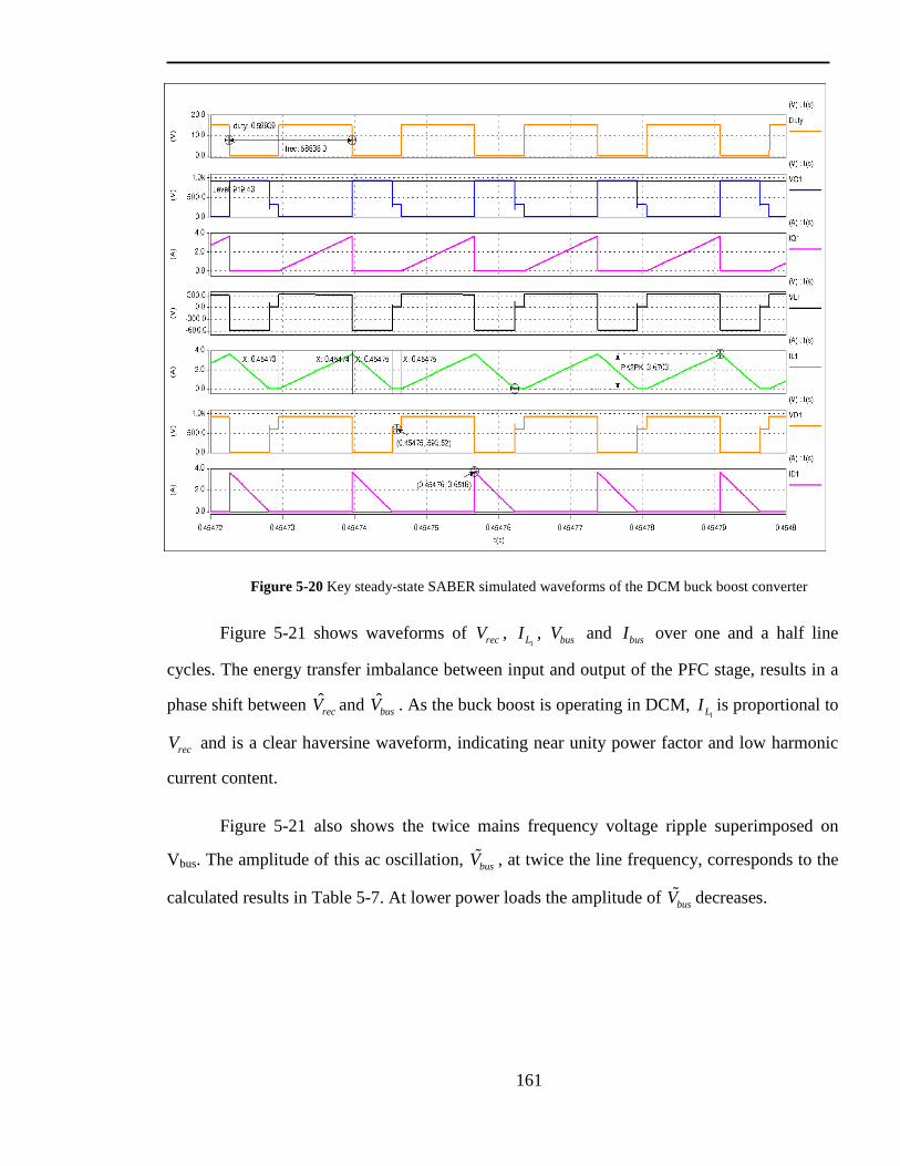
161
Figure 5-20 Key steady-state SABER simulated waveforms of the DCM buck boost converter
Figure 5-21 shows waveforms of recV , 1LI , busV and busI over one and a half line
cycles. The energy transfer imbalance between input and output of the PFC stage, results in a
phase shift between recV and busV . As the buck boost is operating in DCM, 1LI is proportional to
recV and is a clear haversine waveform, indicating near unity power factor and low harmonic
current content.
Figure 5-21 also shows the twice mains frequency voltage ripple superimposed on
Vbus. The amplitude of this ac oscillation, busVɶ , at twice the line frequency, corresponds to the
calculated results in Table 5-7. At lower power loads the amplitude of busVɶ decreases.

162
Figure 5-21 Input current and voltage SABER simulated waveforms of the DCM buck boost converter
Table 5-8 Comparison of key calculated and simulated
Parameter Calculated Simulated Unit
sV 230 230 Vrms
linef 50 50 Hz
swf 60 58.6 kHz
D 0.60 0.59 -
1LV 325 322 V
1 1
ˆ ˆQ DV V= 930 930 V
1 1 1
ˆ ˆ ˆL Q DI I I= = 3.65 3.65 A
1sw nnT t→ 10.10 10.17 sµ
1 2n nt t→ 5.48 5.36 sµ
2 ( 1)n swt n T→ + 1.090 1.08 sµ
busV 600 601 Vrms
busVɶ (at 2 linef× ) 68 68.2 V
,bus fswVɶ 0.60 0.58 V
busI 0.30 0.29 Arms

163
5.11 Power Factor Correction Converter Prototype Design
This section details the prototype PFC converter design, showing the operational
parameters and expected performance. Front end EMC filters are discussed, and designed.
5.11.1 Design Specifications
To summarise the previous design sections, Table 5-9 shows the specifications of the
power factor correction stage, with component values of 1 900L Hµ= and 1 14.1C uF= .
Table 5-9 PFC converter specification
Description Value Unit Input Voltage Vs 230
+10, -6% Vrms
Max Input Current Is 1.0 Arms
Output Voltage Vbus 600 V Output Voltage Ripple
busVɶ 0.6 at swf
69 at linef
V
Output Current Ibus 0.3 A Line Operating Frequency
linef 47-63 Hz
Converter Switching Frequency swf 60 kHz
Output Power Range Pout 60-180 W Efficiency
PFCη 90 % @180 W
Inrush Current Protection - Varistor Power Factor Correction PFC <0.98
Total Harmonic Distortion THD 4 %
5.11.2 EMC Filter
Generally all switching converters have a filter stage at the input to minimise the
injection of high frequency current harmonics into the supply and protect against spurious
electromagnetic interference generated by other equipment. Regulations such as [140] and
[141] limit injected current amplitudes to values typically 40 – 80 dB less than peak 50 Hz
current over a frequency range typically 150 kHz to 30 MHz. Approaches taken to limit EMC
emissions and to limit converter susceptibility take numerous guises. Differential mode filters
limit harmonics generated by the power converter topology between line and neutral.
Common mode filters attenuate the currents flowing through parasitic capacitances between
sources of high dv/dt and earth chassis.

164
EMC is well understood and the filter stage will have little impact on the performance
of the control loop. Therefore the EMC filter is loosely designed to provide token EMC
attenuation of high frequency current harmonics. A SABER simulation of the input EMC
filter, see Figure 5-22, was conducted in order to provide an approximate value of the
harmonic current attenuation. Accurate experimental verification was not performed as
suitable laboratory equipment such as a Line Impedance Stabilization Network, LISN, and a
Spectrum Analyser were not available to optimise the EMC filter and verify design.
Figure 5-22 EMC filter for PFC
The π -filter consisting of ‘X-type’ capacitors C2 and C4, and inductance Lf attenuates
differential mode currents. Capacitors C1, C3, C5 and C6 are all ‘Y-type’ capacitors and provide
a path to earth for the common mode currents.
5.12 Summary
This chapter has presented the requirements and issues of developing a power factor
correction converter for driving HP LEDs. With these issues clearly defined a suitable power
factor correction stage is identified from the converter approaches detailed in Chapter 1, that
can significantly boost the output voltage with respect to the line voltage. This requirement is
due to the limited output capacitance of the metal film capacitors implemented in this PFC, as
electrolytic capacitors, despite their high capacitance, lack the useful operating lifetimes
needed for this application. A brief description of the operation of the steady-state
performance of the PFC is characterised along with the design procedure, fundamental design
equations, magnetic design and expected loss analysis of all devices.

165
Analysis of this approach reveals that due to the lack of any significant output
capacitance of the PFC stage, a large voltage ripple appears at the converter output that has the
ability to draw significant input harmonic currents from the supply if the correct converter
control approach is not adopted.
Finally, SABER switching simulations are shown to validate the theoretical design.

166
6 HP LED Power Factor Correction Control Stage Design
6.1 Introduction
This chapter discusses the issues and control requirements of the HP LED power factor
corrector converter controller. A suitable approach is identified from the methods shortlisted
in Chapter 1. The principles of operation are briefly reviewed and the design of the control
loop is conducted. MATLAB and SABER simulations confirm the operation, stability and
predicted performance of the loop.
6.2 Identification of Control Approach
Section 1.2.5 reviews power factor correction control methods for CCM and DCM
converters. As the buck-boost PFC converter is operating in DCM, commonly implemented
current mode approaches, average and peak control, are not necessary to perform this task.
The simplest approach to DCM PFC control summarised in section 1.2.5, is the single
loop voltage mode control. The control loop needs only to regulate the DC bus voltage and
power throughput. Yet this approach makes the assumption that the output voltage ripple of
the PFC is negligible. This case is not applicable here however, since the use of metal film
capacitors results in a low capacitance and therefore the PFC output bus voltage has a high
ripple component at the 2nd harmonic of the mains supply.
To accommodate this ripple, the functionality of the buck boost DCM voltage loop
controller needs to be addressed. If the voltage control loop was designed for a fast transient
response, the controller would constantly attempt to correct the voltage ripple, causing 2nd
harmonic input current flow. Likewise, if the control compensator bandwidth was limited to
reject twice mains ripple frequency, the transient response of the closed loop system would be
slow, with possible loss of output voltage regulation and even converter failure under line and
load condition changes.
Numerous voltage control loop methods to accommodate this ripple with varying
degrees of success, are detailed in section 1.2.5. The notch filter method [86] is the most
logical approach as the tuned filter would reject the twice mains ripple frequency, allowing
only the high frequency components of the output voltage to be compensated. In order to

167
achieve good results, the filter would require a high Qo factor with exact peak tuning,
otherwise the performance of the filter would be compromised. As the mains frequency is not
always at 50 Hz due to line loading conditions, frequency tracking methods would need to be
employed to ensure accurate filtering. This approach requires high tolerance components and
adds unnecessary expense.
Other solutions proposed are to ‘sample and hold’ the sensed output voltage [86].
Despite effectively eliminating the voltage ripple, should the converter be subject to transient
load or line conditions between sampling periods, the control loop will not respond until the
next sampling period, possibly subjecting converter components to high voltage or current
spikes.
The most suitable approach to limiting the response is regulation band control [86,
142, 143]. This method can accommodate the voltage ripple and minimise converter instability
whilst maintaining a fast transient response to line/load perturbations. Figure 6-1 shows a
practical approach for this controller. Components A1 and A2 are comparators, A3 and A4 are
operational amplifiers. This circuit carries out the following functions. Output voltage, Vbus, is
attenuated by resistors Ra, Rb and Rc and sensed by comparators A1 and A2. The value of Rb
determines the regulation band. If Vbus lies within the regulation band then Da and Db block
the outputs from A1 or A2, and K remains unchanged. If the sensed output voltage leaves the
regulation band due to line or load perturbations, then either comparator A1 or A2 will generate
an output voltage which passes by the appropriate diode and is integrated by the compensator,
comprising components A3, Rd, Rf and Cf.

168
busVrecV
fCfR
busV
1refV
refV
aR
bR
cR
dR
eRgR
hR
recI
recV
aD
bD
1refV
1A
3A
4A
2A
Figure 6-1 Regulation band control block diagram [86]
The output of A3, the voltage K, is multiplied with the attenuated Vrec signal and the
resulting output is compared with the sensed input rectified current, Irec, in A4 to produce an
error voltage for the PWM stage, which in turn generates the duty ratio, D. As there is a
multiplication between K and the Vrec signal in the feedback loop, Rh is used to optimise the
transient response [143].
By implementing regulation band control with A1 and A2 at the input to the integrating
compensator A3, it is ensured that A3 does not respond to voltage perturbations within the
preset dead band, and a fast voltage control response can be achieved with low line current
harmonics.
The stability aspects of this control approach fall into three parts; firstly the setting of
the upper and lower limits of the regulation band. The band needs to be large enough to
include the maximum expected Vbus ripple. If the regulation band is too narrow to
accommodate the ripple, K will vary due to the normal output ripple, and cause distortion of

169
the input line current. Conversely, if the regulation band is too large, the output voltage
regulation will be loosely coupled and over and under voltages may occur, compromising
converter integrity.
Secondly, the response of the controller when the regulation band is exceeded by the
output voltage is critical. Over or undershoot of the output bus voltage may cause the
converter to operate outside its intended region of operation, possibly compromising the
withstand voltages of components connected to Vbus. Thirdly a stable value of K is needed to
maintain the output voltage within the limits during steady state.
The author has modified the proposed control method to enable it to operate in DCM
with a buck-boost converter. The current sense loop is unnecessary when the power stage is
operating in this mode. The author’s improved controller is shown in Figure 6-2, in which the
regulation band method only has to regulate busV .Thus the multiplier, Vrec signal, Rh and A4 in
Figure 6-1 are not required.
busV
1R
2R
lowV
highV
1IC
2IC
3IC
4IC
fCfR
3R
3D
4D
4R
5R
6R
7R
5D
busVrecV
attV
2ICV
1ICV
Figure 6-2 Modified regulation band control for DCM operation

170
6.3 Principles of Operation
Figure 6-2 shows a simplified version of the modified regulation band control for the
DCM buck boost converter. Full schematic diagrams are given in Appendix E. Operation of
the regulation band voltage controller is similar to the previous approach described earlier.
The operation of this control loop is as follows.
The output voltage, Vbus, is attenuated by resistors R1 and R2, and the signal is sensed
by the regulation band comparators IC1 and IC2. If the attenuated Vbus signal, Vatt, is between
reference voltages Vhigh and Vlow, see Figure 6-3, then the outputs of IC1 and IC2 are blocked
by D3 and D4 and K remains unaltered. During this operational state, the controller is
essentially open loop, as there is no continuous feedback loop.
attV
highV
lowV
2ICV
1ICV
railV+ railV−
Figure 6-3 Buck boost output voltage regulation band limits
If V att exceeds the limit Vhigh then IC1 will generate a negative rail voltage which is
passed by D3 to the input of IC3. If Vatt goes below the limit Vlow then IC2 will generate a
positive rail voltage which is passed by D4 to the input of IC3. These signals are integrated by
the operational amplifier IC3 to produce an updated value of K. The output of IC3 is compared
with a reference sawtooth voltage waveform, at switching frequency, swf , by IC4 to produce
the required duty ratio, D. The output signal, D, is now fed directly to the gate drive circuit of
MOSFET Q1 in the power factor corrector.

171
Zener diode, D5, in the feedback loop of the compensator limits the maximum and
minimum voltage error signal K, which in turn limits the maximum and minimum duty ratio.
6.4 Design of Voltage Regulation Band Control
A block diagram of the DCM buck boost and the regulation control loop is shown in
Figure 6-4. It consists of four linear time variant blocks; the voltage compensator, ( )cG s , the
PWM stage, ( )pwmG s , the buck-boost power stage, ( )pG s and the feedback attenuator
( )AKG s . The final block in the diagram is the static nonlinearity, a relay with dead band (R),
which represents the regulation band comparators.
ˆbusv
a
e c dr0( )cG s ( )pwmG s ( )pG s
( )AKG s
Figure 6-4 Control loop block diagram
A small signal analysis of the DCM buck boost converter conducted in [126]
determines the control-to-output transfer function, ( )PG s to be
0
ˆ 0
ˆ( )
ˆ1s
bus dP
v
p
v GG s
sdω
=
= =+
Eqn 6-1
where
0bus
d
VG
D= Eqn 6-2
and

172
1
2p
LR Cω = Eqn 6-3
where pω is the buck boost power stage pole, LR is the equivalent converter load and C1 is the
output capacitance across Vbus. Vbus and D are the steady state output voltage and duty ratio
respectively, and busv , d and ˆsv are small ac perturbations about the quiescent points of Vbus,
D and Vs.
The compensator, ( )CG s , in Figure 6-4 is a Proportional-Integral controller, PI. This
compensator increases the low frequency gain, so that Vbus is well regulated and sets the open
loop zero dB cross over frequency, cf to be below the converter switching frequency, swf .
The transfer function, ( )CG s of this PI compensator is determined by
1
( ) f f fzC C
x
sR R Cs
G s Gs R s
ω∞
+ + = = −
Eqn 6-4
where CG ∞ is the gain of the PI at high frequency and zω is the compensator zero determined
by fC and fR in Figure 6-2. xR is the value of the input resistor to IC3, either R4 or R6
depending on whether limit Vhigh or Vlow has been exceeded.
The PWM stage, ( )pwmG s , is considered linear, therefore the transfer function is
1( )pwm
m
G sV
= Eqn 6-5
where mV is the peak to peak saw tooth voltage of the PWM comparator.
The attenuator, ( )AKG s , transfer function is
2
1
( )AK
RG s
R= Eqn 6-6

173
The first step of the control design is to determine the values of the voltage dead band
limits Vhigh and Vlow. Using Eqn 5-17 the peak to peak voltage ripple of Vbus can be
determined. Table 5-7 lists the steady state parameters of the DCM buck boost PFC operating
in various modes. From this table, the worst case Vbus ripple is identified as busVɶ =68 V at 180
W output. The voltage dead band must not be smaller than the low frequency voltage ripple at
full power. For practicality a 10 % margin has been added to account for component
variability and drift.
The other factors determining control response require a more iterative process. Figure
6-4 can be consolidated and simplified to become Figure 6-5, by combining the transfer
functions CG , pwmG , PG andAKG to become the transfer function H(s), whilst the static
nonlinearity remains as R. The transfer function of H(s) is
( ) ( )AC pwm P KH s G G G G s= Eqn 6-7
The conventional approach of establishing a fast transient response and closed loop
stability by methods of small signal modelling is detailed in [144, 145]. Unfortunately, this
approach is not suitable for loops containing nonlinearities. The proposed method for
achieving stability with a non linearity is based on the circle criterion [146, 147]. This
approach provides a means for analysing nonlinear time-varying systems to obtain system
stability.
R
H(s)
e
a
0 r
Figure 6-5 Simplified model of the buck boost and control

174
The conditions for stability must satisfy
Re[1 ( )] 0zH jω ω+ > ∀ Eqn 6-8
where /z r ε= ∆ ∆ , the slope of the dead band relay seen in Figure 6-6 . The upper and lower
voltage limits of the regulation zone are represented by ε and ε− respectively, and the output
signals of block R, are shown by r and r− .
r
ε−
ε
r−
z
a
R
Figure 6-6 Operation of the relay with dead band
Subsequent Nyquist plots of 1 ( )zH jω+ must remain in the positive sector of the real
axis, Figure 6-7. The values r and r− are determined by the output voltages of IC1 and IC2,
and ε and ε− are predetermined by the attenuator R1 and R2 and the reference values Vhigh
and Vlow in Figure 6-2.
Im
Re0
Figure 6-7 Circle criterion stability requirements

175
6.5 Open Loop Analysis
This section details the analysis of the open loop system of blocks R and ( )H s and
analysis is conducted using MATLAB. Plots of the control to output transfer function of the
DCM buck boost converter, the PWM stage, the attenuator, the gain of the voltage dead band
relay and the PI voltage compensator are given. When operating in DCM, the duty ratio of the
buck boost converter and therefore its bode plot is affected by the load. Eqn 6-1 is plotted for
a nominal input voltage, Vs= 230 Vrms, at either output voltage limit, -640 V and -560 V. The
output power is varied from full power, 180 W, to minimum power, 60 W.
Figure 6-8 Control-to-output magnitude and phase plots of the buck-boost converter, Vs=230 Vrms,
Pout=180 W, (a) Vbus= -640 V, (b) Vbus= -560 V

176
(a)
(b)
Figure 6-9 Control-to-output magnitude and phase plots of the buck boost converter, Vs=230 Vrms,
Pout=120 W, (a) Vbus= -640 V, (b) Vbus= -560 V

177
Figure 6-10 Control-to-output magnitude and phase plots of the buck boost converter, Vs=230 Vrms,
Pout=60 W, (a) Vbus= -640 V, (b) Vbus= -560 V
A summary of the key points of these plots is given in Table 6-1. With an increase of
power output the low frequency gain decreases whilst the frequency of the pole and the zero
dB cross over point increases. With these characteristics in mind, the frequency of the PI
compensator zero is critical.

178
Table 6-1 Summary of control-to-output, ( )pG s , phase and gain bode plots at various loads
Vs (Vrms)
Vbus (V)
Pout (W)
Gain @ low frequency
(dB)
pf
(Hz) cf
(kHz)
230 -640 180 59.1 9.92 9.03 230 -560 180 57.8 12.92 10.3 230 -640 120 60.9 6.60 6.96 230 -560 120 59.6 8.60 8.22 230 -640 60 63.9 3.30 5.77 230 -560 60 62.6 4.30 5.90
The magnitude and phase of the PWM stage, ( )pwmG s , are constant at -20 dB and zero
degrees for all frequencies. The magnitude and phase of the attenuator stage, ( )AKG s , are
constant at -40 dB and zero degrees for all frequencies.
The voltage dead band relay, block R, is modelled at its maximum gain, i.e. when
either limit Vhigh or Vlow is exceeded by the attenuated Vbus voltage. From Figure 6-6,
parameters ‘r’ and ‘-r’, ± 12 V. The limits ‘ε ’ and ‘-ε ’, are Vhigh and Vlow, -5.6 V and -6.4 V.
Therefore using /z r ε= ∆ ∆ , the magnitude and phase of the voltage dead band relay are given
by 29.5 dB and zero degrees for all frequencies.
Now that transfer functions ( )pG s , ( )pwmG s , ( )AKG s and R have been defined, the PI
compensator, ( )CG s , can be designed to ensure a stable closed loop system whilst achieving a
fast response. The requirement for the open loop gain is that it should be high at low
frequencies to minimise steady state error, the cross over frequency,cf , should be
approximately an order of magnitude below swf , and the magnitude gain plot should cross the
zero dB axis with a slope of -20 dB per decade [45]. To achieve a high open loop gain cross
over frequency, the gain of the PI needs to be high. The result of this is that when Vbus reaches
V low, the PI will compensate by decreasing its output, K, to momentarily stop the PWM stage
switching. The input current, Is, will be interrupted, possibly causing a current surge at the
next MOSFET turn on and an increase in input current harmonics.

179
Using the MATLAB control toolbox SISOTOOL, the maximum gain of the
compensator can be determined to ensure closed loop system stability whilst ensuring
acceptable phase and gain margin of the open loop.
6.6 Proportional Integrator Compensator Design
This section shows the results of the empirical methods used to determine the position
of the compensator zero and the respective gain using the MATLAB control toolbox
SISOTOOL. Simulations show that placing the zero of the PI compensator at a slightly higher
frequency than the pole of the buck boost power stage results in the real part of
1 ( )zH jw+ crossing into the negative plane, thus not satisfying the Circle Criterion.
For Figure 6-8 to Figure 6-10, frequencies above pf , the magnitude decays at – 20
dB/dec. In order to achieve an open loop zero dB crossover slope of -20 dB/dec, for block R
and ( )H s , the zero of the linear compensator needs to be situated at a lower frequency than
the pole of the power stage, otherwise a -40 dB/dec slope would occur at the zero dB
crossover point.
From Table 6-1, the lowest value of the control-to-output pole of the power stage is 3.3
Hz, therefore by ensuring the PI compensator zero frequency is below this value, the system
stability can be assured for all operating conditions. A bode plot of the PI compensator is
shown in Figure 6-11, where the zero is at 1.6 mHz, and the high frequency gain is 32 dB.

180
zf
Figure 6-11 Bode plot of ( )CG s
The resulting transfer function of the linear compensator in Figure 6-11 is
39 0.39( )C
sG s
s
− −= Eqn 6-9
6.7 Voltage Loop Response at Regulation Band Limits
As the control loop is effectively open when Vbus is within the voltage regulation band,
the output is unregulated. Hence system stability and response is only of concern when Vbus
exceeds the limits. Therefore the following analysis looks only at the stability occurring at
these boundaries. Figure 6-12 (a) shows the magnitude and phase plots of ( )zH s , where
/z r ε= ∆ ∆ , at nominal Vs, an output power of 180 W and when the attenuated Vbus signal,
Vatt, is more negative than Vlow. The compensator zero, zf , is at a lower frequency than the
power stage single pole, pf , allowing for a –20 dB/dec slope at the zero dB cross over
frequency, and a 90° phase lead. Figure 6-12 (b) is the Nyquist plot of 1 ( )zH jω+ at the same
input and output conditions. It can be seen that the Circle Criterion is satisfied for stability, as

181
the entire plot remains in the positive half of the real axis. For clarity, Figure 6-12 (c) is a
close up of the real axis of Figure 6-12 (b).
Figure 6-13 (a) shows the magnitude and phase plots of ( )zH s , at nominal Vs, an
output power of 180 W and when Vatt is more positive than Vhigh. As before, the compensator
zero, zf , is below the power stage single pole, pf , allowing for a –20 dB/dec slope at the zero
dB cross over frequency, and a 90° phase lead. Figure 6-13 (b) is the Nyquist plot of
1 ( )zH jω+ at the same input and output conditions. It can be seen that the Circle Criterion is
satisfied for stability, as the entire plot remains in the positive portion of the real axis. For
clarity, Figure 6-13 (c) is a close up of the real axis of Figure 6-13 (b).
zf pf
cf
zf pf
cf
Figure 6-12 (a) Magnitude and phase of ( )H s and R, (b) & (c) plots of 1 ( )zH jω+ for Vs= 230
Vrms,Vbus= -640 V and Pout= 180 W.

182
zf pf
cf
Figure 6-13 (a) Magnitude and phase of ( )H s and R, (b) & (c) plots of 1 ( )zH jω+ for Vs= 230
Vrms,Vbus= -560 V and Pout= 180 W
Figure 6-14 and Figure 6-15 again plot the magnitude and phase diagrams of ( )zH s
and a Nyquist plot of 1 ( )zH jω+ for a nominal Vs of 230 Vrms, an output voltage exceeding
Vhigh and Vlow, however the output power is reduced to 120 W.

183
(a)
(b) (c)
zf pf
cf
Figure 6-14 (a) Magnitude and phase of blocks ( )H s and R, (b) & (c) plots of 1 ( )zH jω+ for Vs=
230 Vrms,Vbus= -640 V and Pout= 120 W

184
(a)
(b) (c)
zf pf
cf
Figure 6-15 (a) Magnitude and phase of ( )H s and R, (b) & (c) plots of 1 ( )zH jω+ for Vs= 230
Vrms,Vbus= -560 V and Pout= 120 W
Finally Figure 6-16 and Figure 6-17 plot the magnitude and phase diagrams of ( )zH s
and a Nyquist plot of 1 ( )zH jω+ for a nominal Vs of 230 Vrms, an output voltage exceeding
Vhigh and Vlow, however the output power is reduced to 60 W.

185
(a)
(b) (c)
zf pf
cf
Figure 6-16 (a) Magnitude and phase of ( )H s and R, (b) & (c) plots of 1 ( )zH jω+ for Vs= 230
Vrms,Vbus= -640 V and Pout= 60 W

186
zf pf
cf
Figure 6-17 (a) Magnitude and phase of blocks ( )H s and R, (b) & (c) plots of 1 ( )zH jω+ for Vs=
230 Vrms,Vbus= -560 V and Pout= 60 W
Table 6-2 summarises the frequencies of the PI compensator zero, and the power stage
pole at a fixed Vs but with varying values of Pout and Vbus. It can be seen, that under the
various line and load conditions, pf , cf and the gain change. The tables shows that the cross
over frequency of ( )H s and R varies from 5.22 kHz at (Vs=230 V, Vbus=-640 V, Pout=60 W),
to a maximum of 10.3 kHz at (Vs=230 V, Vbus= -640 V, Pout= 180 W).
A final point of observation to be made of Table 6-2, is the consistent phase margin of
90ο . As zf is below pf , the 90ο phase lag of pf dominates the phase at cf , thus ensuring

187
stability of the open loop system. Generally a phase margin of 45ο to 60ο is used in a control
system for a fast response [45], however this is not achievable in this instance. From [148] a
phase margin of 90ο relates to a damping ratio of 3.0. This ensures that there is no overshoot
or oscillation of the open loop system to a step load or input voltage change.
Table 6-2 Summary of Figure 6-12 to Figure 6-17
Vs (V)
Vbus (V)
Pout (W)
zf (mHz)
pf
(Hz) cf
(kHz)
Gain (dB)
Phase Margin
( ο)
230 -640 180 1.6 9.92 10.3 60.7 90 230 -560 180 1.6 12.92 10.1 57.8 90 230 -640 120 1.6 6.60 8.67 62.5 90 230 -560 120 1.6 8.60 9.59 61.2 90 230 -640 60 1.6 3.30 5.22 63.8 90 230 -560 60 1.6 4.30 6.83 64.2 90
6.8 SABER Simulation PI Compensator Design
From the results detailed previously for the SISOTOOL simulated PI compensator, the
experimental component values for compensator A3 were found to be R1= 990 kΩ, R2= 10
kΩ, R3,4,5,6= 51 kΩ, R7= 102 kΩ, Rf= 20 kΩ, Cf= 0.5 µF and D5= 7.8 V zener.
6.9 SABER Simulation Verification of Control Loop
The results of the MATLAB control analysis were verified with a SABER simulation.
The control block, in Figure 6-18, consists of the converter output feedback attenuator, and an
extra operational amplifier acting as a buffer to avoid loading the resistor chain, the non linear
relay with voltage dead band, the PI voltage compensator, a saw tooth waveform generator,
the PWM stage comparator and a gate drive interface. The feedback attenuator reduces Vbus by
a factor of 100. Regulation dead band limits Vhigh and Vlow are set by ideal voltage sources of
-5.6 V and – 6.4 V respectively. A fixed 60 kHz saw tooth waveform is generated by an
LM555 timer and fed to the PWM stage comparator to be compared with the output of the PI
compensator.
The following simulations demonstrate the dynamic performance of the DCM buck-
boost converter with the proposed voltage regulation band control. The results presented are

188
all for a nominal input voltage Vs=230 Vrms with the output power, Pout, varying in a stepped
manner. Ideal operational amplifiers were used in the simulation, thus there is no offset
voltage at the input of the PI compensator to introduce a positive or negative drift in K, hence
making D vary and Vbus drift between voltage limits.
Figure 6-18 SABER simulation schematic of control loop and PFC converter
The following plots, Figure 6-19 to Figure 6-21, show the converter control loop
response being subjected to a step load change of 0 W to 60 W, 0 W to 120 W and 0 W to 180
W. At 80.0 ms there is no load across the output capacitor, C1, and K is low to prevent
MOSFET switching and charging of C1. At 0.1 s the step load occurs, causing the voltage
across C1 to reduce. The control loop does not respond until Vbus reaches the upper voltage
limit, - 560 V. The capacitor C1 is the only source of energy to the load before the upper
voltage limit is reached. The control loop only regulates Vbus when the -560 V limit is
exceeded, as is seen by an increase in K at around 0.11 s. The response of K in these figures is
such that it does not overcompensate Vbus, due to the 90ο phase margin, forcing it towards the
lower voltage boundary, -640 V, where the control loop again would have to correct, causing
further oscillations.

189
Figure 6-19 SABER Vbus response to step load 0 W to 60 W
Figure 6-20 SABER Vbus response to step load 0 W to 120 W

190
Figure 6-21 SABER Vbus response to step load 0 W to 180 W
During the step load change, Vbus repeatedly becomes more positive than limit Vhigh for
a number of cycles despite the PI compensator attempting to regulate Vbus back within the
voltage regulation band. The maximum output voltage of the compensator, K, is limited by
zener diode D5, and a high frequency oscillation can be seen during the cross over of Vbus at
around 0.11 s as K increases and the natural 100 Hz ripple of Vbus attempts to pull the voltage
beyond the regulation band. This high frequency oscillation can be eliminated by reducing the
gain of the PI compensator, which will in turn reduce the band width of the open loop stage.
However, reducing the PI compensator gain would cause Vbus to sag significantly during step
load increases, and the subsequent constant current power stages to operate beyond their
specifications.
For this application step load changes would only occur at the turn on of the LED
constant current regulators. Other step load conditions to which the application may be subject
are those when the LED string is required to dim or brighten. Figure 6-22 details the converter
subject to a change in load from 0 W to 60 W with step load increases to 120 W and finally
180 W at 10 ms, 0.1 s and 0.3 s respectively. Figure 6-23 shows the converter subject to a
change of load from 0 W to 180 W followed by step load decreases to 120 W and 60 W, at 5
ms, 0.1 s and 0.3 s.

191
Figure 6-22 SABER Vbus response to step load from 0 W to 60 W to 120 W to 180 W
Figure 6-23 SABER Vbus response to step load from 0 W to 180 W to 120 W to 60 W
From these simulations it can be seen that the simulated model of the power stage and
its control loop are performing as expected and are suitable for this application.
6.10 Summary
This chapter has presented a thorough analysis of a modified regulation band voltage
controller for a HP LED power factor correction converter. Due to the implications of the
performance characteristics of the PFC stage, a suitable control loop had to be realised that

192
whose operation would regulate the PFC output voltage, but would not generate any
significant input current harmonics. A modified regulation band controller detailed in Chapter
1 is developed that fulfils this criterion.
A detailed description of operation of this method is discussed and the dynamics of the
control loop are analysed. Due to the non linearity presented by the regulation band, Circle
Criterion is applied to determine the system loop stability whilst MATLAB and SABER
simulations validate the initial theoretical analysis. Finally a discrete regulation band
controller is designed for implementation in a proof of concept prototype.
An important contribution of this chapter is the development, analysis and design of a
control approach that has not been presented in any literature for this application. This work
forms part of a conference paper and presentation at the IEEE Power Electronics, Machines
and Drives, 2008, York.

193
7 Experimental Verification and System Performance
7.1 Introduction
This chapter details the prototype development of the HP LED driver designed in
Chapters 5 and 6. After a review of the HP LED driver requirements the design of a current
regulator and control approach is conducted with SABER simulations to validate the design.
The development of the prototype HP LED driver, PFC and regulator stage is undertaken
showing the layout and tracking of the two topologies. Finally, the prototypes experimental
measurements are compared with the predicted SABER and MATLAB simulation models.
7.2 HP LED Constant Current Regulators
This section details the design of the power topology and control approach for
regulating the current through each of the three LED strings introduced in section 5.2. High
power LED devices need to be supplied with a regulated current. The current flow through
them defines the lumens output. In order to achieve a regulated LED current, whilst
minimising peak current and voltage ripple stresses, a secondary converter is required. The
LED power system arrangement detailed in Figure 5-3 shows a front end PFC delivering a
regulated Vbus and unity power factor, and three strings of high power LEDs. Each string of
LEDs is independently current regulated. In order to achieve a lumen output of 8,000 lm, 144
HP LEDs are necessary, in this case arranged in three separate strings. Each LED string
comprises of 48 LEDs in series. The maximum voltage across a string at 350 mA is around
180 V at Tj = 50 C. As Vbus is -600 V, a step down converter is required to supply each LED
string with a regulated constant current. Section 1.2.3 identifies the buck converter as a
topology able to perform this step down conversion. To maintain simplicity, achieve high
reliability and efficiency, the buck converter can operate in near Critical Current Conduction
Mode, CCCM see Figure 7-1, to perform current regulation. By not using an output filter
capacitor while in this operating mode, long operation lifetime can be realised and a simple
method of converter control realised. Control methods identified in Section 1.2.5, show that
simple hysteretic control would meet the regulation needs.

194
7.3 Principles of Operation of the Constant Current Converter
Figure 7-1 shows the schematic of the buck converter and a block diagram of the
hysteretic control loop. Along with Figure 7-2, the operation of this converter stage is as
follows. During t0 to t1, MOSFET AQ is on, and ( )AL bus ledV V V= − appears across inductor AL .
ALI increases from ,minALI to
,maxALI . When ALI reaches
,A setLI , transistor AQ turns off. Diode AD
is reversed biased during this period.
busV
AQV
ALV
ledV
ADV
AQI
ALI
,A senseLI
V0
V600−
AQ
AD
ALADI
,A setLI
Figure 7-1 Constant current buck regulator with control
The time t0 to t1 is given by
,max ,min
1 0
( )A A
A
A L L
L
L I It t
V
−− = Eqn 7-1
During the period 1t to 0 Aswt T+ the current in the inductor falls from ,maxALI to
,minALI ,
and diode AD conducts.

195
( ),max ,min
0 1( ) A A
A
A L L
swled
L I It T t
V
−+ − = Eqn 7-2
0t 1t 0 Aswt T+busV
busV
,A setLI
,minALI
ledV
bus ledV V−
,maxALI
AswDT (1 )AswD T−
0
0
0
0
0
0
AQV
ADV
AQI
ALI
ALV
ADI
Figure 7-2 Key waveforms of buck converter

196
When ,minALI is reached, AQ is turned on again and the cycle repeats. The average
current through the HP LEDs is
,max ,min
, 2A A
A ave
L L
L
I II
+= Eqn 7-3
The buck converter operates close to boundary conduction current mode, i.e. ,minALI is
nearly zero.
By using this method simple hysteretic current control is possible. Hysteretic operation
eliminates the need for small-signal control loop compensation. To reduce the average current
supplied to the HP LED string, ,maxALI needs to be reduced so that the required value of
,A aveLI is
reached. The value of,maxALI is set by the circuit to be equal to
,A setLI , a control voltage input
level. So ,A aveLI is adjusted by controlling
,A setLI , either from a separate voltage source or via a
potentiometer. There is a consequential change in switching frequency from approximately 40
kHz to 80 kHz for an average supply current to the LEDs of 350 mA to 100 mA. Switching
the HP LED string at these frequencies will not cause stroboscopic effects.
7.4 Control of Buck Converter
Figure 7-3 shows a diagram of one buck converter hysteretic controller. The HP LED
current flows through a sense resistor, senseR creating a voltage signal which is inverted and
amplified by a factor of 10 by the instrumentation amplifier, 1AIC . The output waveform is
applied to the inverted pin of comparator, 2AIC . The feedback components 2AR , 3AR and 1AD
form the Schmitt trigger. The upper and lower limits are not set by 2AR and 3AR . The lower
Schmitt trigger level is determined by voltage ,minA setL , and the upper Schmitt trigger level is
set by ,A setLI .
The output from 2AIC is a square wave, which is a function of the amplified sensed
inductor current and the upper and lower voltage limits of the Schmitt trigger. This signal is
applied to the gate drive circuits switching MOSFET.

197
ALV
senseR
,minA setL
AL
1AIC
2AIC
auxV+
,A setLI
1AR
2AR
3AR
1AD
auxV+2AD
Figure 7-3 Buck Control block diagram
7.5 Constant Current Converter Optimisation
This section details the buck converter design optimisation as well as inductor design
and component selection. The principles of operation in the previous section outline the key
design equations to help identify the most appropriate inductance, which will in turn realise
the optimum frequency operating range and power loss.
With LA= 5 mH, Table 7-1 details the key calculated operating conditions at a constant
input voltage and at minimum and maximum power.
Table 7-1 Key calculated values of constant current converter at minimum and maximum load
Parameter 30 W 60 W Unit Vbus -600 -600 V Duty 0.31 0.31 - Fsw 86.4 40.0 kHz ILA,pk -0.32 -0.65 A ILA,ave -0.16 -0.32 A VQA=VDA -600 -600 V IQA,rms 0.10 0.2 A IDA,rms 0.15 0.3 A V led -186 -186 V

198
Using the magnetic design approach in section 2.2.4, a summary of the buck magnetic
component design can be found in Table 7-2. The same core material and type as the PFC
inductor was used again due to its availability and performance characteristics. The relative
size of the core allowed the magnetic core and conduction losses to be minimised to a
minimum in order to maintain converter stage efficiency.
A power loss break down of the converter operating at full power, 60 W, is detailed in
Table 7-3. The power losses of the interconnecting cables, tracks and connectors are ignored.
At maximum output the total estimated power loss is 2.70 W, a theoretical converter
efficiency of 95 %. A slight increased efficiency to 96.4 % (2.2 W loss) of the converter can
be achieved by reducing the buck inductance. However the result of this would be a marked
increase in maximum operating frequency to 205 kHz, which is near the optimum operating
limit of the magnetic core material and increased EMC interference with the rest of the HP
LED lighting system.
Table 7-2 Characteristics of constant current converter inductor
Parameter Calculated Unit Core manufacturer Ferroxcube - Core type RM12 - Core material 3C90 - Core factor 0.38 mm-1
Effective volume 8340 mm3
Effective length (m) 55.6 mm Effective area 146 mm2
Mean turn length 61 mm Initial permeability 1730 - Effective permeability 30.9 - Air gap 0.5 mm Inductance factor 351 nH Inductance 5.1 mH Number of turns 119 - Flux 26.8 uW Flux density 189 mT Wire length 7.30 m Current density 3.00 A/mm2
Wire resistance 13.5 Ω Copper loss @ 100 °C 1.85 W Core loss @ 100 °C 0.25 W Total losses @ 100 °C 2.10 W

199
Table 7-3 Estimated power losses of converter at full load
Component Device Switching Loss (W)
Conduction Loss (W)
Core Loss (W)
Total Loss (W)
QA STP10NK70Z 0.16 0.05 - 0.21 DA RHRP8120 0.08 0.311 - 0.391 LA RM12 - 1.85 0.25 2.10
Total Estimated Power Loss 2.70
7.6 Constant Current Regulator Specifications
To summarise the previous design sections, Table 7-4 details the specification of the
current regulator stage.
Table 7-4 Current regulator specifications
Description Value Unit Input Voltage Vbus 600 ±5 % V
Max Input Current Ibus 122 mA
Output Voltage Vled 180 ±2 % V Output Voltage Ripple
busVɶ 5 V
Output Current ILed 350 mA Converter Switching Frequency
swf 40-86 kHz
Output Power Range Pout 30-60 W Efficiency
PFCη 95 % @ 60 W
7.7 Constant Current SABER Simulation
The predicted design calculations of the power stage and the hysteretic control loop
were verified in a SABER model. Figure 7-4 shows the simulation schematic of the HP LED
constant current regulator. The MOSFET is an ideal device with negligible on-state resistance
and high off-state resistance. The power diodes are all piece wise linear components with no
forward volt drop. The power inductor is also a linear device with no parasitic ESR and
interwinding capacitance.

200
The key simulated results plotted in Figure 7-5 are captured where the input voltage
Vbus is set to -600 V with a power output delivered to the HP LEDs of 60 W. The results show
a close correlation to the predicted design detailed in Table 7-1.
Figure 7-4 SABER simulation model of constant current HP LED regulator
Figure 7-5 SABER simulation of key waveforms of constant current HP LED regulator
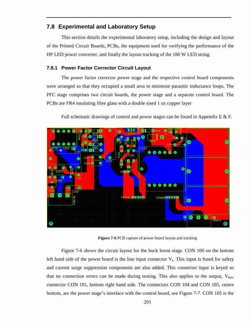
201
7.8 Experimental and Laboratory Setup
This section details the experimental laboratory setup, including the design and layout
of the Printed Circuit Boards, PCBs, the equipment used for verifying the performance of the
HP LED power converter, and finally the layout tracking of the 180 W LED string.
7.8.1 Power Factor Corrector Circuit Layout
The power factor corrector power stage and the respective control board components
were arranged so that they occupied a small area to minimise parasitic inductance loops. The
PFC stage comprises two circuit boards, the power stage and a separate control board. The
PCBs are FR4 insulating fibre glass with a double sised 1 oz copper layer
Full schematic drawings of control and power stages can be found in Appendix E & F.
Figure 7-6 PCB capture of power board layout and tracking
Figure 7-6 shows the circuit layout for the buck boost stage. CON 100 on the bottom
left hand side of the power board is the line input connector Vs. This input is fused for safety
and current surge suppression components are also added. This connector input is keyed so
that no connection errors can be made during testing. This also applies to the output, Vbus,
connector CON 101, bottom right hand side. The connectors CON 104 and CON 105, centre
bottom, are the power stage’s interface with the control board, see Figure 7-7. CON 105 is the

202
Vbus feedback and CON 104 is the output of the gate driver. As the buck boost MOSFET
Q100, is not directly referenced to ground, an isolating pulse transformer T100, is used to
transfer the low side voltage gate signal from the control loop, to the high side connected
MOSFET, Q100. The RM12 buck boost inductor is labelled device L103 in Figure 7-6 and the
metallised film capacitors C111-C113. All inputs and outputs were capacitively decoupled to a
copper earth plane, so to ensure EMC suppression.
The control board, see Figure 7-7, consists of the output voltage Vbus attenuator, the
relay with dead band, the linear PI compensator, a sawtooth waveform generator to supply the
PWM comparator, MOSFET gate drive circuitry and auxiliary ± 15 V supplies provided by
onboard linear regulators. Again, use of space was minimised to ensure compactness and
efficiency. There are also numerous test points situated across both circuit boards for ease of
testing.
Figure 7-7 PCB capture of control circuit layout and tracking
Figure 7-8 is a picture of the DCM buck boost PFC and its associated control board.

203
Figure 7-8 HP LED experimental PFC stage
7.9 Constant Current Regulator Circuit Layout
The HP LED current regulators comprise three identical power converters. The buck
regulator is a physically compact design to minimise parasitic loops, and minimise EMC
generation. The PCB is of FR4 fibre glass with a double sided 1 oz copper layer. The same
principles of design and layout were applied. Power connectors were keyed and minimum
voltage clearances were observed as to prevent voltage creep. The input connector, CON200,
is fused to provide protection should the LED string fail to a short circuit. As the buck
MOSFET Q200, source is connected to -600 V, an isolating pulse transformer T200, is used to
transfer the low side voltage gate signal from the control loop, to the MOSFET. The power
inductor LA is labelled L200 in this layout, and is also a shielded RM core.
A start up oscillator that momentarily pulses a signal to the input of the comparator
which provides a leading edge on which the converter can start switching. The pulse
frequency is sufficiently low enough so not to interfere with steady state operation.
Input Filter & Rectifier
Metal Film Capacitors
Control Board
MOSFET & Diode
DCM Inductor

204
Figure 7-9 PCB layout of constant current buck regulator
Once the PCBs had been populated testing of the prototype boards used the following
to acquire and record experimental data; a Lecroy WaveRunner oscilloscope along with a high
voltage differential probe ADP305 and a passive AP105 current probe, were used to capture
voltage and current waveforms. A Yokogawa WT3000 power analyser recorded and assessed
the line voltage, current waveform quality and harmonic content. Laboratory set-up is shown
in Figure 4-3.
7.10 HP LED String
In order to fully test the performance of the converter stages, and to realise whether
they are suitable for this application, an LED string was constructed, see Figure 7-10, the
measured outer dimensions of which are 216 mm by 520 mm. The total display consists of
three individual strings of 48 ultra white Cree XLamp XR series HP LEDs. These high power
devices emit a lumens output of 70 lm/w at a current throughput of 350 mA.
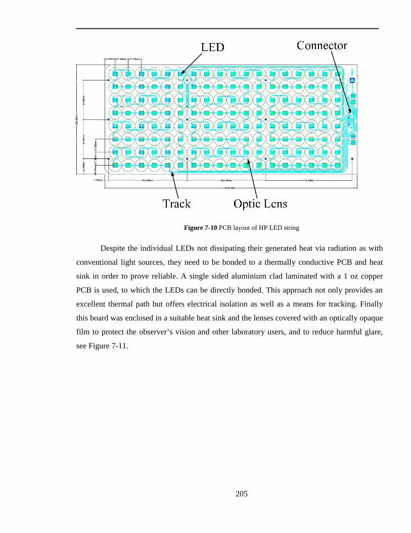
205
Figure 7-10 PCB layout of HP LED string
Despite the individual LEDs not dissipating their generated heat via radiation as with
conventional light sources, they need to be bonded to a thermally conductive PCB and heat
sink in order to prove reliable. A single sided aluminium clad laminated with a 1 oz copper
PCB is used, to which the LEDs can be directly bonded. This approach not only provides an
excellent thermal path but offers electrical isolation as well as a means for tracking. Finally
this board was enclosed in a suitable heat sink and the lenses covered with an optically opaque
film to protect the observer’s vision and other laboratory users, and to reduce harmful glare,
see Figure 7-11.

206
Figure 7-11 HP LED strings and protective cover
7.11 Verification and Results
This section validates the calculated design, computer simulations and experimental
data of both the power factor corrector and the respective LED current regulators.
Experimental results show the compatibility of the ability of the PFC to be able to meet
harmonic regulations and maintain a sinusoidal input current waveform, Is, in phase with its
respective voltage Vs.
7.11.1 Power Factor Corrector
Key design equations and converter operational parameters are detailed in Section 5.9.
Table 5-7 lists a number of key design figures predicting the various peak currents and
voltages that the components are subject to. All figures presented make the assumption that
the converter is operating under ideal conditions, i.e. no parasitic elements.
Table 1-1 in Chapter 1 details the Class C harmonic limits for all lighting equipment
rated above 25 W. The first ten specified limits are plotted against the measured input current
harmonics of the PFC stage. Again like Table 5-7, the input current harmonics in Figure 7-12
are taken at a nominal input voltage over three various output power loads. It can be seen that
all input harmonics fall well within the specified limits, especially that of the second harmonic

207
that has been all but eliminated by the control approach. The measured power factor of the
system was near unity at 0.99.
Table 7-5 Measured parameters of PFC
Parameter Test 1 Test 2 Test 3 Unit Input Voltage, Vs 216 230 265 Vrms Input Current, Is 0.94 0.86 0.74 Irms Input Power, Pin 203.4 200.2 198 W Apparent Power, Sp 203.6 201 198.6 VA Reactive Power, Qp 8.48 8.11 9.46 VAr Power Factor, PF 0.998 0.999 0.998 - Phase Angle, θ 2.39 2.35 2.74 Vs THD 0.93 0.93 0.93 - Is THD 5.08 5.108 5.57 - Output Voltage, Vbus 602 595 599 Vrms
Output Current, Ibus 0.29 0.30 0.30 Irms
Output Power, Pout 179.8 180.1 180.2 W Efficiency, η 88 90 91 %

208
0
5
10
15
20
25
30
35
2 3 5 7 9 11 13 15 17 19
Harmonic
Har
mo
nic
as
a %
of
Fu
nd
amen
tal
HarmonicLimit
ExperimentalHarmonic
(a)
0
5
10
15
20
25
30
35
2 3 5 7 9 11 13 15 17 19
Harmonic
Har
mo
nic
as
a %
of
Fu
nd
amen
tal
HarmonicLimit
ExperimentalHarmonic
(b)
0
5
10
15
20
25
30
35
2 3 5 7 9 11 13 15 17 19
Harmonic
Har
mo
nic
as
a %
of
Fu
nd
amen
tal
HarmonicLimit
ExperimentalHarmonic
(c)
Figure 7-12 Input current harmonics at 230sV V= (a) 60 W, (b) 120 W, (c) 180 W output
.

209
7.11.2 Buck boost steady state experimental waveforms
In this section the recorded steady state experimental waveforms of the buck-boost
PFC. These signals are superimposed and compared with the SABER simulated waveforms to
verify the performance and operation of the prototype. The following steady state plots are
captured at an input voltage of Vs,nom, at various load conditions.
Figure 7-13 Comparison of simulation and experimental results for Vs=230 Vrms at Pout=60 W
Excellent correlation between simulated and experimental waveforms can be seen, in
terms of similar wave shapes and magnitudes. Due to parasitic observations observed in
Section 4.4, parasitic components are modelled, hence the high frequency oscillations
occurring during the DCM in the simulated steady state waveforms. However there are some
minor discrepancies that are worth noting. Again there is a slight mismatch between the
switching frequency of the simulation and the prototype. This is due to prototype component
tolerances in the PWM oscillator. Switching interference is observed on the experimental
waveforms of the duty cycle of all figures. The frequency of this interference corresponds to
the switching frequency of the cascaded buck converter. EMC suppression approaches

210
diminish this interference to the magnitudes seen in Figure 7-13 to Figure 7-15, and do not
degrade the performance of the PFC power stage or the control loop.
Parasitic elements of the prototype were introduced to the simulation model to improve
the accuracy and verify the performance. Again close relationship of the parasitic oscillations
can be seen apart from the damping ratio.
Figure 7-14 Comparison of simulation and experimental results for Vs=230Vrms at Pout=120W
Figure 7-15 shows the PFC operating at full power and with an input line voltage of
230 Vrms. The converter can clearly be seen to be operating close to the limit of discontinuous
current mode. Parasitic oscillations are not evident in both the simulated or experimental
waveforms as the dead time is near zero. The operating mode of the PFC tends to near critical
current conduction mode as the input voltage approaches Vs,min. Experimental observations
show that critical conduction mode is not realised unless the supply voltage exceeds its
defined limits.

211
Figure 7-15 Comparison of simulation and experimental results for Vs=230Vrms at Pout=180W
Besides the parasitic elements of the switching semiconductor, of which one has no
control, there is very little leading or trailing edge current or voltage spikes, owing to the
careful and compact circuit layout.
7.11.3 Parasitics
Note the oscillations of the simulated SABER waveforms and that of the measured
experimental waveforms during Toff. The oscillation observed during the period that the
inductor current falls to zero is due parasitic inductances and capacitive components, most
notably during low load, 60 W. Figure 7-16 details these main components such as track
inductance, semiconductor capacitances, and inductor winding capacitance. Track inductance
can be deemed to be negligible as the layout is compact. The semiconductor capacitances can
easily be determined by referring to their respective datasheet.

212
1Q
busV
busI
1L
1D
1CbusRrecV
1LR
1LC
dsCjC
trackL
gdC gsC
1CR
1CL
Figure 7-16 Parasitic components of buck boost
The winding capacitance of the inductor L1 is more difficult to determine. In order to
realise this parameter an HP-3577B Network Analyser was used to determine the resonant
frequency. An impedance measurement over a frequency spread of 10 kHz to 5 MHz
determines the resonant frequency, rf to be approximately 1.8 MHz. Using
1 21
1L
r
Cw L
= Eqn 7-4
where 1
rr
wf
= , the winding capacitance becomes 9 pF. From Figure 7-17 the high
frequency of the measured oscillation was determined to be 467 kHz. Further investigation
showed the oscillation to be excited by the inductance L1 and output capacitance Coss of the
MOSFET. The MOSFET output capacitance,oss ds gdC C C= + , is 174 pF. These parasitic
components were simulated and a comparison can also be seen in Figure 7-17. The conditions
for this figure are Vs=230 Vrms, Vbus=-629 V, Pout=60 W, Fsw=58 kHz, Duty= 0.36. These
oscillations are difficult to suppress with a typical resistor, capacitor, diode, RCD,
combination without excessive power dissipation.

213
Figure 7-17 Comparison of simulated and experimental parasitic components
The resonance damping seen in the experimental measurements is due to track
resistance and inductor resistance, which is difficult to estimate for a simulation. These
parasitic components are now included in the simulation for all line and load conditions and
the results can be seen in the next section.
7.11.4 Buck boost transient experimental waveforms
The transient response of the prototype converter is shown in this section were it
undergoes step load changes. The key waveforms captured are the output power step load,
Pout, the output signal of the PI compensator, K, the buck boost inductor current, IL1, and
finally the output voltage, Vbus.
Figure 7-18 shows the PFC being subject to a step load change of 0 to 60 W at time 18
ms. When the step load change occurs, the output capacitors are discharged and Vbus tends to
zero. Upon exceeding the predetermined voltage bandwidth of -560 V 18 ms later, the PI
controller responds by increasing K, which increases the switching duty ratio and bringing
Vbus back within the limits. At this point K maintains its level until another transient. The
calculated and simulated models are verified by the performance of the prototype. The 100 Hz
output voltage ripple, busVɶ , the peak current 1ˆLI and the response time in the below figures are
the same as those calculated and predicted by models.

214
Figure 7-18 Experimental results of PFC output with a step load of 0 W to 60 W
Figure 7-19 Experimental results of PFC output with a step load of 0 W to 120 W
A disparity between the simulated and experimental measurements is the DC offset of
Vbus when it is within the voltage bandwidth. In this state the power converter is in an open
loop condition therefore it is not possible to capture the same voltage level twice. The same is
true for the value of signal K.

215
Figure 7-20 Experimental results of PFC output with a step load of 0 W to 180 W
Figure 7-21 Experimental results of PFC output with a step load of 60 W to 120 W
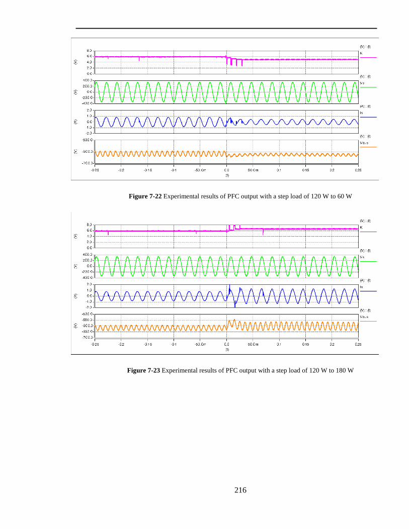
216
Figure 7-22 Experimental results of PFC output with a step load of 120 W to 60 W
Figure 7-23 Experimental results of PFC output with a step load of 120 W to 180 W

217
Figure 7-24 Experimental results of PFC output with a step load of 180 W to 120 W
Figure 7-25 Experimental results of PFC output with a step load of 60 W to 180 W

218
Figure 7-26 Experimental results of PFC output with a step load of 180 W to 60 W
7.12 Summary
This chapter details the design and development of a simplified critical conduction
mode buck converter and its respective hysteretic controller to regulate the current through
each of the HP LED strings. SABER simulations performed confirm the suitability of this
approach prior to the prototype buck regulator being developed and tested.
A laboratory set up is shown for the evaluation of the performance of the HP LED
power converter system and the bank of HP LEDs to achieve the 8,000 lm is tracked out and
populated. The experimental results of the PFC stage are shown, revealing that the converter
and the regulation band control operate as predicted. The 2nd harmonic of the input current is
well within specified limits, and the regulation band control regulates the output PFC bus
voltage with good transient response at the band limits and showing loop stability under
steady-state conditions.

219
8 Conclusions and Further Work
8.1 Introduction
Power electronic development has always been driven by the advancement of new
design techniques and emerging technologies. It is these innovations that have led to the recent
advances in active power factor correction methods and the commercial release of high power
light emitting diodes.
A comprehensive literature review identifies the main issues and requirements to
successfully develop these technologies, input current harmonic limits are specified, power
converter operating conditions are described, suitable power/control methods are reviewed,
magnetic modelling techniques are identified and finally a discussion of the current
development status of power components is included.
8.2 Summary of the Thesis
The merging of advanced power topology techniques and integrated magnetic
approaches had led to the development of a single-stage, single-switch power factor corrector
with an integrated magnetic component. A suitable power converter topology has been
identified that can perform single-stage power factor correction and which can accommodate
the integration of a complex magnetic component. This magnetic device combines the
functions of a DCM boost inductor and a power transformer. Steady-state analysis of the
power converter and state-by-state description of the operation provide an understanding of
the complex waveforms and enabled the design and development of an integrated magnetic
prototype. The construction of the IM ensured that the S4PFC was able to operate unaffected
by the IM whilst achieving optimum performance.
To confirm the operating principles and design of the converter and magnetic
component, steady-state SABER switched modelling was conducted. The simulation also
allowed the operating conditions of the magnetic core to be examined, in particular to check
that the saturation limits were not exceeded. The simulation results correlated closely with
initial design predictions and showed that the input current harmonics complied with
regulations. Steady-state simulations did highlight however the limitations of the S4PFC,

220
namely, under light load conditions, the boost voltage increases as it is not directly regulated
by the controller.
Small-signal models of the S4PFC were developed and the dynamic performance of the
power stage was characterised by MATLAB simulations. The results showed that the control-
to-output transfer function is similar to that of a non-isolated CCM buck converter, and the
input-to-output transfer function, neglecting any input filtering, is similar to that of a DCM
boost converter in series with a CCM buck converter. These dynamic characteristics suggest
that a simple voltage-mode control can be implemented to perform output regulation. A PID
control loop was designed and modelled using MATLAB and SABER which ensured that the
S4PFC was stable under transient conditions and had a fast transient response. A 180 W
prototype S4PFC with an IM was developed, and the measured results verified the theoretical
and simulated steady-state operation and dynamic performance.
High power light emitting diodes offer numerous advantages over current lighting
solutions in terms of light quality, efficiency and useful operating lifetimes. However one of
the main factors limiting the take up of HP LEDs is the comparatively poor lifetime of many
of the power electronic converters used to supply them which is due to the use of electrolytic
capacitors to provide energy storage and hold-up capabilities.
In contrast metal film capacitors can operate for up to 100,000 hours, even over large
temperature variations, but have significantly lower capacitance than electrolytics however
they withstand much higher voltages. Therefore to realise the necessary energy storage
requirements of a power factor correction stage, using long-lifetime capacitors, the output
voltage of this stage must be increased.
A buck-boost topology operating in discontinuous current mode was identified as the
most suitable topology for the HP LED PFC stage as it can achieve both automatic input
current wave-shaping, limiting current harmonics, and provide a high output voltage. Steady-
state analysis was performed to verify the approach, but indicated that due to the low PFC
stage output capacitance, there was a significant twice-line-frequency voltage ripple at the
output. As the input harmonic current limits are more tightly regulated for lighting equipment,
a control approach was identified that would provide output regulation but would not process

221
the 100 Hz ripple voltage, thereby preventing the ripple voltage from propagating around the
control loop and disturbing the input current.
A modified regulation band voltage mode controller was developed and designed. A
SABER simulation was performed and analysis, based on the circle critereon was used to
determine the stability conditions. MATLAB simulations verified this approach, and provided
a basis for the design of a regulation band controller. SABER simulations of the regulation
band controller and PFC stage validated the theoretical design.
To regulate the current through the HP LEDs, a secondary constant current buck
regulation stage was developed and simulated. A 180 W prototype HP LED power factor
corrector and constant current converter validated the theoretical and simulated predictions.
8.3 Contributions of this Research
To the best of the authors knowledge, there is no previously published work that
examines an integrated magnetic component with a single-stage, single-switch power factor
corrector. The analysis presented in this Thesis details the flux waveforms that occur within
the core of the integrated magnetic in this topology. The solution that has been developed
offers a well utilised core and optimised winding arrangement.
The dynamic analysis of the S4PFC with an IM has not been undertaken previously. By
determining the S4PFC line-to-output and control-to-output transfer functions, suitable control
approaches were identified and demonstrated.
To address the limited lifetime of current power supplies for HP LEDs, the author
proposes a power topology and control solution that uses metal film capacitors instead of
electrolytics for the PFC output stage, and the resulting increased output voltage ripple is
regulated by adopting a modified regulation band control approach.
This controller regulates the PFC output voltage within defined limits, with a fast,
stable response at these boundaries, whilst limiting the generation of the second harmonic
input current. Circle criterion analysis is used to evaluate the dynamic performance of the
regulation band control loop and the closed loop stability of the HP LED power system.

222
8.4 Future Development
Analysis and operating results of the S4PFC indicates that due to the unregulated DCM
boost output voltage and increased current though the MOSFET, this device is particularly
stressed. Therefore the MOSFET that meets these requirements is invariably more expensive
than that used in a two-stage PFC approach. As semiconductor technology invariably
advances, then the piece cost of these devices will drop, making this approach much more
attractive for future designers.
Due to the complex winding structure of the IM device for the S4PFC, this approach
may be unattractive due to cost and assembly considerations. An alternative construction
approach would be to use planar magnetic structures, in which the windings are either etched
on to PCBs or stamped out copper sheets. This approach overcomes the need for custom coil
formers, and may also enable more rapid prototyping and automated assembly.
As HP LEDs become more widely used and as the size of HP LED strings increase,
higher capacity power supplies will be required and further research is therefore needed to
identify optimium solutions, for example to determine whether interleaved power factor
corrector approaches can be realised using the regulation band controller. The possibility of
current imbalances between the interleaved topologies must be examined, which might
interfere with regulation, stability and input current harmonic content.
One possible alternative application of the HP LEDs is in communication systems
where the LED string would pulse at high frequency, far beyond the range of human
perception. Investigations need to be conducted as to whether the regulation band control
approach is still suitable for this application.

223
References
[1] "Electromagnetic compatibility (EMC)-Part 3-2: Limits — Limits for harmonic
current emissions (equipment input current k 16 A per phase)," in BS EN61000-3-2:2006 European Standard, 2006.
[2] A. Peres, D. C. Martins, and I. Barbi, "ZETA converter applied in power factor correction," in Power Electronics Specialists Conference, PESC '94 Record., 25th Annual IEEE, 1994, pp. 1152-1157 vol.2.
[3] J. S. Lai and D. Chen, "Design consideration for power factor correction boost converter operating at the boundary of continuous conduction mode and discontinuous conduction mode.," in APEC '93. Conference Proceedings, 1993, pp. 267-273.
[4] W. Tsai-Fu and C. Yu-Kai, "Analysis and design of an isolated single-stage converter achieving power-factor correction and fast regulation," Industrial Electronics, IEEE Transactions on, vol. 46, pp. 759-767, 1999.
[5] I. M. Huai Wei, and Issa Batarseh, IEEE Senior Member, "Comparison of Basic Converter Topologies For Power Factor Correction," IEEE, 1998.
[6] M. R. Sahid, N. A. Azli, and N. D. Muhammad, "A comparative study on the performances of the boost PFC circuit," in Power and Energy Conference, 2004. PECon 2004. Proceedings. National, 2004, pp. 143-147.
[7] C. Sudhakarababu and M. Veerachary, "Zeta converter for power factor correction and voltage regulation," in TENCON 2004. 2004 IEEE Region 10 Conference, 2004, pp. 61-64 Vol. 4.
[8] S. Ang and A. Oliva, Power-Switching Converters, 2nd ed. New York: Taylor & Francis, 2005.
[9] O. Semiconductor, "Power Factor Correction Handbook ", 2007, pp. 1-52. [10] K. Billings, Switchmode Power Supply Handbook, Second ed. New York: McGraw-
Hill., 1999. [11] R. Redl and L. Balogh, "Power-Factor Correction in Bridge and Voltage-Doubler
Rectifier Circuits with Inductors and Capacitors," Applied Power Electronics Conference and Exposition. , pp. 466 - 472 1995.
[12] M. Jovanovic and D. E. Crow, "Merits and limitations of full-bridge rectifier with LC filter in meeting IEC 1000-3-2 harmonic-limit specifications," Industry Applications, vol. Volume: 33, pp. 551 - 557, March-April 1997
[13] "Electromagnetic compatibility (EMC)-Part 3-2: Limits for harmonic current emissions (equipment input current 16 A per phase)," in BS EN61000-3-2:2006 European Standard, 2006.
[14] L. B. Richard Redl, Nathan O. Sokal, "Design Considerations for Single-Stage Isolated Power-Factor Corrected Power Supplies with Fast Regulation of the Output Voltage," Applied Power Electronics Conference and Exposition, 1995. APEC '95. Conference Proceedings 1995., Tenth Annual pp. 5-9 March 1995 5-9 March 1995 1995.
[15] F. Zheng, X. Yang, and W. Zhaoan, "A general way to find the integrated magnetics topology," in Power Electronics and Motion Control Conference, 2004. IPEMC 2004. The 4th International, 2004, pp. 1170-1173 Vol.3.

224
[16] R. Severns and G. Bloom, "Modern DC-to-DC Switchmode Power Converter Circuits," New York: Van Nostrand Reinhold, 1985.
[17] S. Chandrasekaran and L. U. Gokdere, "Integrated magnetics for interleaved DC-DC boost converter for fuel cell powered vehicles," in Power Electronics Specialists Conference, 2004. PESC 04. 2004 IEEE 35th Annual, 2004, pp. 356-361 Vol.1.
[18] F. Zheng, H. Weihao, Y.-q. Pei, and A. Y. X. Yang Xu, "A Novel Analysis and Design Method for Integrated Magnetics," in Power Electronics and Motion Control Conference, 2006. IPEMC '06. CES/IEEE 5th International, 2006, pp. 1-4.
[19] W. Chen, G. Hua, D. Sable, and F. A. L. F. Lee, "Design of high efficiency, low profile, low voltage converter with integrated magnetics," in Applied Power Electronics Conference and Exposition, 1997. APEC '97 Conference Proceedings 1997., Twelfth Annual, 1997, pp. 911-917 vol.2.
[20] X. Peng, W. Qiaoqiao, W. Pit-Leong, and F. C. A. L. F. C. Lee, "A novel integrated current doubler rectifier," in Applied Power Electronics Conference and Exposition, 2000. APEC 2000. Fifteenth Annual IEEE, 2000, pp. 735-740 vol.2.
[21] W. Leung-Pong, L. Yim-Shu, and C. David Ki-Wai, "A new approach to the analysis and design of integrated magnetics," in Applied Power Electronics Conference and Exposition, 2001. APEC 2001. Sixteenth Annual IEEE, 2001, pp. 1196-1202 vol.2.
[22] G. B. Crouse, "Electrical Filter," in US Patent 1 920 948, 1933. [23] A. Lloyde, "Choking up on LC filters," in Electron. Mag, 1967. [24] J. Cielo and H. Hoffman, "Combined transformer and inductor device," in US Patent 3
553 620, 1971. [25] G. C. Waehner, "Switching power supply common outout filter," in US Patent 3 916
286, 1975. [26] G. E. Bloom, "New integrated magnetic dc dc power converter circuits and systems,"
APEC '87, pp. 57-66. [27] C. T. A. Johnk, Engineering Electromagnetic Fields and Waves. New York: Wiley &
Sons, 1975. [28] G. Calderon-Lopez, A. J. Forsyth, and D. R. Nuttall, "Design and Performance
Evaluation of a 10-kW Interleaved Boost Converter for a Fuel Cell Electric Vehicle," in Power Electronics and Motion Control Conference, 2006. IPEMC '06. CES/IEEE 5th International, 2006, pp. 1-5.
[29] "Luxeon Reliability Datasheet RD25," Philips Lumileds, 2006. [30] P. Clarke, "Seoul pushes Acriche LED to 150 lumens per watt," in EE Times, 2010. [31] "Pocket Guide to High Intensity Discharge Lamp Ballasts," Philips Lighting, 2009. [32] W. N. Charman, "Night myopia and driving," Ophthal. Physial. Opt., vol. 16, pp. 474-
485, 1996. [33] S. J. Anderson and I. E. Holliday, "Night driving: effects of glare from vehicle
headlights on motion perception," Ophthal. Physial. Opt., vol. 15, pp. 545-551, 1995. [34] N. Narendran, Y. Gu, J. P. Freyssinier, H. Yu, and L. Deng, "Solid-state lighting:
failure analysis of white LEDs," Journal of Crystal Growth, vol. 268, pp. 449-456, 2004.
[35] S. Muthu and J. Gaines, "Red, green and blue LED-based white light source: implementation challenges and control design," in Industry Applications Conference, 2003. 38th IAS Annual Meeting. Conference Record of the, 2003, pp. 515-522 vol.1.

225
[36] R. Simpson, "Are compact fluorescent lamps with integral ballasts fit to replace incandescent lamps," in UKDL Newsletter, 2007, pp. 34-45.
[37] A. J. Zele and A. J. Vingrys, "Defining the detection mechanisms for symmetric and rectified flicker stimuli," Vision Research, vol. 47, 2007.
[38] K. Chauhan and W. N. Charman, "Accomodation responses to flickering stimuli," Ophthal. Physial. Opt., vol. 16, pp. 391-408, 1996.
[39] "Application Brief AB11- Electrical Drive Information Luxeon Products," Philips Lighting, 2006.
[40] "Evox Rifa," in Life Limiting Factors in Electrolytic Capacitors, 2001, pp. 1-6. [41] "Code of practice for the design of road lighting. Part 1: Lighting of roads and public
amenity areas," in BS EN 5489-1:2003 United Kingdom, 2003. [42] "Road lighting Part 2: Performance requirements," in BS EN 13201-2: 2003 United
Kingdom, 2003. [43] "EVOX RIFA," in Datasheet PEH 200 Long Life Electrolytic Capacitor, 2007. [44] A. Nishino, "Capacitors: operating principles, current market and technical trends,"
Journal of Power Sources, pp. 137-147, 1996. [45] T. M. U. Ned Mohan, William P. Robbins, Power Electronics: Converters
Applications and Design: John Wiley & Sons., 1989. [46] A. I. Pressman, Switching Power Supply Design, 2nd ed. New York: McGraw-Hill,
1998. [47] P. Krein, Elements of Power Electronics. New York: Oxford University Press, 2000. [48] A. R. Prasad, P. D. Ziogas, and S. Manias, "A novel passive waveshaping method for
single-phase diode rectifiers," in Industrial Electronics Society, 1990. IECON '90., 16th Annual Conference of IEEE, 1990, pp. 1041-1050 vol.2.
[49] J. Spangler and A. K. Behera, "Power factor correction techniques used for fluorescent lamp ballasts," in Industry Applications Society Annual Meeting, 1991, pp. 1836-1841
[50] C. S. Moo, H. C. Yen, Y. C. Hsieh, and Y. C. Chuang, "Integrated design of EMI filter and PFC low-pass filter for power electronic converters," Electric Power Applications, IEE Proceedings vol. 150, pp. 39-44, 2003.
[51] K. Taniguchi and Y. Nakaya, "Analysis and improvement of input current waveforms for discontinuous-mode boost converter with unity power factor," Power Conversion Conference - Nagaoka, vol. 1 3-6 Aug. 1997
[52] C. K. Tse and M. H. L. Chow, "New single-stage power-factor-corrected regulators operating in discontinuous capacitor voltage mode," in 28th Annual IEEE Power Electronics Specialists Conference, , 1997, pp. 371-377.
[53] K. Hirachi and M. Nakaoka, "Improved control strategy on buck-type PFC converter," Electronics Letters, vol. 34, pp. 1162-1163, 1998.
[54] I. G. Z. K. Huai Wei Batarseh, P. , "A single-switch AC-DC converter with power factor correction," Power Electronics, IEEE Transactions on, vol. Volume: 15 pp. 421 - 430, May 2000 2000
[55] H. Tae-Won, S. Young-Dae, and S. Enrico, "Analysis of the interleaved type power factor correction (PFC) converter in discontinuous current mode," in 30th Annual Conference of IEEE Industrial Electronics Society 2004, pp. 2706-2711
[56] R. Teodorescu, S. B. Kjaer, S. Munk-Nielsen, F. Blaabjerg, and J. K. Pedersen, "Comparative analysis of three interleaved boost power factor corrected topologies in

226
DCM," in Power Electronics Specialists Conference, 2001. PESC. 2001 IEEE 32nd Annual, 2001, pp. 3-7 vol. 1.
[57] M. Oscar García, IEEE, José A. Cobos, Member, IEEE, Roberto Prieto, Member, IEEE, Pedro Alou, and and S. M. Javier Uceda, IEEE, "Single Phase Power Factor Correction: A Survey," 2003.
[58] L. Shiguo, W. Huai, Z. Guangyong, and I. A. B. I. Batarseh, "Several schemes of alleviating bus voltage stress in single stage power factor correction converters," in Proceedings of the IEEE International Conference on Power Electronics and Drive Systems 1999, pp. 921-926
[59] M. H. Kheraluwala, R. L. Steigerwald, and R. Gurumoorthy, "A fast-response high power factor converter with a single power stage," in 22nd Annual IEEE Power Electronics Specialists Conference 1991, pp. 769-779.
[60] S. M. Chongming Qiao, IEEE, and Keyue Ma Smedley, Senior Member, IEEE, "A Topology Survey of Single-Stage Power Factor Corrector with a Boost Type Input-Current-Shaper," IEEE Transactions on Power Electronics, vol. 16, pp. 360 - 368 May 2001.
[61] M. T. Madigan, R. W. Erickson, and E. H. Ismail, "Integrated high-quality rectifier-regulators," IEEE Transactions on Industrial Electronics, vol. 46, pp. 749 - 758, Aug 1999
[62] M. M. Jovanovic, D. M. C. Tsang, and F. C. Lee, "Reduction of voltage stress in integrated high-quality recitifier regulators by variable frequency control," IEEE, pp. 569-575, 1994.
[63] Q. Jinrong, Z. Qun, and F. C. Lee, "Single-stage single-switch power-factor-correction AC/DC converters with DC-bus voltage feedback for universal line applications," IEEE Transactions on Power Electronics, vol. 13, pp. 1079-1088, 1998.
[64] I. Takahashi and R. Y. Igarashi, "A switching power supply of 99% power factor by the dither rectifier," 13th International Telecommunications Energy Conference pp. 714 - 719 5-8 Nov 1991
[65] Z. Guangyong, C. Iannello, P. Kornetzky, and I. Batarseh, "Large-signal modeling of a single-switch power factor correction converter," in IEEE 31st Annual Power Electronics Specialists Conference 2000, pp. 1351-1357.
[66] K. Schenk and S. Cuk, "A single-switch single-stage active power factor corrector with high quality input and output," Power Electronics Specialists Conference, 1997. PESC '97 Record., 28th Annual IEEE, vol. Volume: 1 pp. 385 - 391, 22-27 June 1997 1997
[67] R. Ayyanar, N. Mohan, and S. Jian, "Single-stage three-phase power-factor-correction circuit using three isolated single-phase SEPIC converters operating in CCM," in IEEE 31st Annual Power Electronics Specialists Conference 2000, pp. 353-358
[68] R. Redl, L. Balogh, and N. O. Sokal, "A New Family of Single-Stage Isolated Power-Factor Correctors with Fast Regulation of the Output Voltage," IEEE Power Electronics Specialists Conference, pp. 1137-1143, 1994.
[69] L. Huber and M. M. Jovanovic, "Design optimization of single-stage single-switch input-current shapers," IEEE Transactions on Power Electronics vol. 15, pp. 174 - 184 Jan 2000

227
[70] F.-S. Tsai, P. Markowski, and E. Whitcomb, "Off-line flyback converter with input harmonic current correction," IEEE 18th International Telecommunications Energy Conference, pp. 120 - 124 6-10 Oct 1996.
[71] Z. Qun, F. C. Lee, and T. Fu-sheng, "Voltage and current stress reduction in single-stage power factor correction AC/DC converters with bulk capacitor voltage feedback," IEEE Transactions on Power Electronics, vol. 17, pp. 477-484, 2002.
[72] J. A. Villarejo, J. Sebastian, A. Fernandez, M. M. Hernando, and P. J. A. Villegas, "Optimizing the design of single-stage power factor correctors," in 17th Annual IEEE Applied Power Electronics Conference and Exposition 2002, pp. 231-236.
[73] D. Weihua, Z. Bo, and H. Zongbo, "Analysis of a novel boundary conduction mode (BCM) and voltage control of buck capacitor in single-stage PFC circuit," in 4th International Power Electronics and Motion Control Conference 2004, pp. 126-131
[74] D. D. C. Lu, H. H. C. Lu, and V. Pjevalica, "A Single-Stage AC/DC Converter with High Power Factor, Regulated Bus Voltage and Output Voltage," in Industrial Electronics Society, 2007. IECON 2007. 33rd Annual Conference of the IEEE, 2007, pp. 1455-1460.
[75] M. Z. Youssef and P. K. Jain, "A Novel Single Stage AC/DC Self-Oscillating Series-Parallel Resonant Converter," IEEE Transactions on Power Electronics, vol. 21, pp. 1735-1744, 2006.
[76] M. S. Agamy and P. K. Jain, "A new zero voltage switching single stage power factor corrected three level resonant AC/DC converter," in 31st Annual Conference of IEEE Industrial Electronics Society, 2005, pp. 1178-1183.
[77] M. S. Agamy and P. K. Jain, "A discrete time controller for a single stage three level resonant PFC converter operated with variable frequency phase shift modulation," in 29th International Telecommunications Energy Conference 2007, pp. 242-247.
[78] M. S. Agamy and P. K. Jain, "A single stage three level resonant LLC AC/DC converter," in 21st Annual IEEE Applied Power Electronics Conference and Exposition, 2006, pp. 411-416.
[79] S. A. Mohammed and K. J. Praveen, "A Comparative Study of Two Controllers for Single Stage Three-Level AC/DC Converters," in Canadian Conference on Electrical and Computer Engineering 2006, pp. 235-238.
[80] L. Rossetto, G. Spiazzi, and P. Tenti, "Control Techniques for Power Factor Correction Converters," Power Electonics Motion and Control, 1994.
[81] J. Lloyd H. Dixon, "Current mode control of Switching Power Supplies," in Unitrode Product & Applications Handbook, 1994.
[82] L. Jiaying and W. Xiaobo, "A Novel Piecewise Linear Slope Compensation Circuit in Peak Current Mode Control," EDSSC pp. 929-932, 20-22 Dec. 2007.
[83] E. J. P. Mascarenhas, "Hysteresis control of a continuous boost regulator," in IEE Colloquium on Static Power Conversion, 1992, pp. 7/1-7/4.
[84] J. Mahdavi and A. K. Shahriari, "Comparison of conducted RFI emission from different unity power factor AC/DC converters," in Sixth International Conference on Power Electronics and Variable Speed Drives 1996, pp. 132-137.
[85] J. S. Lai and D. Chen, "Design consideration for power factor correction boost converter operating at the boundary of continuous conduction mode and discontinuous conduction mode," in Applied Power Electronics Conference and Exposition, 1993. APEC '93. Conference Proceedings 1993., Eighth Annual, 1993, pp. 267-273.

228
[86] J. B. Williams, "Design of feedback loop in unity power factor AC to DC converter " Power Electronics Specialists Conference, vol. 959-967 June 1989.
[87] C. M. Kellett, S. Hyungbo, and A. R. Teel, "Further results on robustness of (possibly discontinuous) sample and hold feedback," Automatic Control, IEEE Transactions on, vol. 49, pp. 1081-1089, 2004.
[88] C. Spiazzi, P. Mattavelli, and L. Rossetto, "Power factor preregulators with improved dynamic response," Power Electronics, IEEE Transactions on, vol. 12, pp. 343-349, 1997.
[89] P. Zumel, O. Garcia, J. A. Cobos, and J. Uceda, "Magnetic integration for interleaved converters," in Applied Power Electronics Conference and Exposition, 2003. APEC '03. Eighteenth Annual IEEE, 2003, pp. 1143-1149 vol.2.
[90] P. W. Lee, Y. S. Lee, K. W. Cheng, and X. C. Lui, "Steady-State Analysis of an Interleaved Boost Converter with Coupled Inductor," IEEE Tranactions on Industrial Electronics, vol. 47, pp. 787-795, August 2000.
[91] J. W. Kolar, G. R. Kamath, N. Mohan, and F. C. Zach, "Self-adjusting input current ripple cancellation of coupled parallel connected hysteresis-controlled boost power factor correctors," in Power Electronics Specialists Conference, 1995. PESC '95 Record., 26th Annual IEEE, 1995, pp. 164-173 vol.1.
[92] W. Pit-Leong and F. C. Lee, "Interleaving to reduce reverse recovery loss in power factor correction circuits," in Industry Applications Conference, 2000. Conference Record of the 2000 IEEE, 2000, pp. 2311-2316 vol.4.
[93] H. Xudong, W. Xiaoyan, T. Nergaard, L. Jih-Sheng, X. Xingyi, and Z. Lizhi, "Parasitic ringing and design issues of digitally controlled high power interleaved boost converters," Power Electronics, IEEE Transactions on, vol. 19, pp. 1341-1352, 2004.
[94] L. Dylan Dah-Chuan, D. K. W. Cheng, and L. Yim-Shu, "A single-switch continuous-conduction-mode boost converter with reduced reverse-recovery and switching losses," Industrial Electronics, IEEE Transactions on, vol. 50, pp. 767-776, 2003.
[95] P. Cantillon-Murphy, T. C. Neugebauer, C. Brasca, and D. J. Perreault, "An active ripple filtering technique for improving common-mode inductor performance," Power Electronics Letters, IEEE, vol. 2, pp. 45-50, 2004.
[96] G. W. Ludwig and S. A. El-Hamamsy, "Coupled inductance and reluctance models of magnetic components," Power Electronics, IEEE Transactions on, vol. 6, pp. 240-250, 1991.
[97] A. A. Aboulnaga and A. Emadi, "Simplified simulation and modeling technique for integrated magnetic components in power electronic converters," in Telecommunications Energy Conference, 2004. INTELEC 2004. 26th Annual International, 2004, pp. 725-730.
[98] D. C. Hamill, "Gyrator-capacitor modeling: a better way of understanding magnetic components," in Applied Power Electronics Conference and Exposition, 1994. APEC '94. Conference Proceedings 1994., Ninth Annual, 1994, pp. 326-332 vol.1.
[99] L. Yim-Shu, W. Leung-Pong, and D. K. W. Cheng, "Simulation and design of integrated magnetics for power converters," Magnetics, IEEE Transactions on, vol. 39, pp. 1008-1018, 2003.

229
[100] G. Calderon-Lopez, "Design and Control of the Dual-Interleaved Boost Converter with Interphase Transformer," in School of Electrical and Electronic Engineering. vol. Doctor of Philosophy: The University of Manchester, 2009.
[101] G. M. Dolny, "High-voltage semiconductor devices: status and trends," in Bipolar/BiCMOS Circuits and Technology Meeting, 2005. Proceedings of the, 2005, pp. 78-85.
[102] R. Singh, J. A. Cooper, Jr., M. R. Melloch, T. P. Chow, and J. W. Palmour, "SiC power Schottky and PiN diodes," Electron Devices, IEEE Transactions on, vol. 49, pp. 665-672, 2002.
[103] A. Elasser, M. H. Kheraluwala, M. Ghezzo, R. L. Steigerwald, N. A. Evers, J. Kretchmer, and T. P. Chow, "A comparative evaluation of new silicon carbide diodes and state-of-the-art silicon diodes for power electronic applications," Industry Applications, IEEE Transactions on, vol. 39, pp. 915-921, 2003.
[104] A. R. Hefner, Jr., R. Singh, L. Jih-Sheg, D. W. Berning, S. Bouche, and C. Chapuy, "SiC power diodes provide breakthrough performance for a wide range of applications," Power Electronics, IEEE Transactions on, vol. 16, pp. 273-280, 2001.
[105] S. Sawant and B. J. Baliga, "A comparative study of high voltage (4 kV) power rectifiers PiN/MPS/SSD/SPEED," in Power Semiconductor Devices and ICs, 1999. ISPSD '99. Proceedings., The 11th International Symposium on, 1999, pp. 153-156.
[106] M. Mori, H. Kobayashi, and Y. Yasuda, "6.5 kV ultra soft & fast recovery diode (U-SFD) with high reverse recovery capability," in Power Semiconductor Devices and ICs, 2000. Proceedings. The 12th International Symposium on, 2000, pp. 115-118.
[107] M. R. Krames, O. B. Shchekin, R. Mueller-Mach, G. O. Mueller, L. Zhou, G. Harbers, and M. G. Craford, "Status and Future of High-Power Light Emitting Diodes for Solid-State Lighting," Journal of Display Technology, vol. 3, pp. 160-175, June 2007.
[108] "LED Lighting Technology: Lessons from the USA," Department of Trade and Industry, 2007.
[109] Y. H. Huang, C. L. Cheng, T. T. Chen, Y. F. Chen, and K. T. Tsen, "Studies of Stokes shift in InGaN alloys," Journal of Applied Physics, vol. 101, pp. 103521-103521-4, 2007.
[110] "Ecodesign Directive (2005/32/EC)," European Energy Commission, 2009. [111] Luxeon, "Power light source LUXEON K2 Technical Datasheet," Philips
Semiconductor April 2007 2007. [112] C. Semiconductors, "Cree XLamp LED Thermal Management," 2006. [113] O. Semiconductors, "Thermal Management of OSTSAR Projection Light Source,"
2006. [114] S. Semiconductor, "Z Power LED Thermal Management Guide," 2005. [115] N. Semiconductor, "Nichia Thermal Management Design of LEDs," 2003. [116] M. D. Bobde and B. J. Baliga, "Silicon planar ACCUFET: improved power MOSFET
structure," Electronics Letters, vol. 36, pp. 913-915, 2000. [117] S. Tsengyou, P. Venkatraman, and B. J. Baliga, "Comparison of ultralow specific on-
resistance UMOSFET structures: the ACCUFET, EXTFET, INVFET, and conventional UMOSFET's," Electron Devices, IEEE Transactions on, vol. 41, pp. 800-808, 1994.

230
[118] J. A. Cooper, Jr. Melloch, M.R. Singh, R. Agarwal, A. Palmour, J.W. , "Status and prospects for SiC power MOSFETs," IEEE transactions on Electron Devices, vol. 49, pp. 658-664, 2002.
[119] L. A. Lipkin, "Low interface state density oxides on p-type SiC," Silicon Carbide, III-Nitrates and Related Materials, p. 853, 1998.
[120] L. A. Lipkin and J. W. Palmour, "Improved oxidation procedures for reduced SiO/SiC defects," Journal of Electonic Materials, vol. 25, p. 909, 1996.
[121] M. Gurfinkel, J. Suehle, J. B. Bernstein, Y. Shapira, A. J. Lelis, D. Habersat, and N. Goldsman, "Ultra-Fast Characterization of Transient Gate Oxide Trapping in SiC Mosfets," in Reliability physics symposium, 2007. proceedings. 45th annual. ieee international, 2007, pp. 462-466.
[122] T. Williams, EMC for Product Designers. Oxford: Elsevier, 2006. [123] "Road lighting Part 1: Selection of lighting classes," in BS EN 13201-1: 2004 United
Kingdom, 2004. [124] "Luminaires-Part 1: General requirements and tests," in BS EN 60958-1:2004 United
Kingdom, 2004. [125] "Degrees of protection provided by enclosures (IP code)," in BS EN 60529-1: 1992
United Kingdom, 1992. [126] R. W. Erickson and D. Maksimovic, Fundamentals of Power Electronics: Kluwer
Academic Publishers Group, 2001. [127] D. D. C. Lu, H. H. C. Lu, and V. Pjevalica, "Single-stage AC/DC boost-forward
converter with high power factor, regulated bus and output voltages," in Circuits and Systems, 2009. ISCAS 2009. IEEE International Symposium on, 2009, pp. 2645-2648.
[128] K. Yao, X. Ruan, X. Mao, and Z. Ye, "Variable Duty Cycle Control to Achieve High Input Power Factor for DCM Boost PFC Converter," Industrial Electronics, IEEE Transactions on, vol. PP, pp. 1-1.
[129] E. Kreyszig, Advanced Engineering Mathematics, 8th ed. New York: John Wiley & Sons, 1999.
[130] Ferroxcube, "Data Handbook Soft Ferrites and Accessories," 2008. [131] C. W. T. McLyman, Magnetic Core Selection for Transformers and Inductors, 2 ed.
New York: Marcel Dekker, 1997. [132] R. C. Dorf and R. H. Bishop, Modern Control Systems, 8 ed. New York: Prentice Hall,
1997. [133] R. Ridley, "Designing with the TL431," in Switching Power Magazine, 2005, pp. 1-5. [134] Faichild, "TL431/TL431A Programmable Shunt Regulator," 2003. [135] C. P. Basso, Switch-Mode Power Supplies Spice Simulations and Practical Designs.
New York: McGraw-Hill, 2008. [136] Texas-Instruments, "UC2842 Current Mode PWM Controller ", 2001. [137] "EVOX RIFA," in Datasheet PHE450 Double metallized film capacitor, 2007. [138] "Road lighting Part 4: Methods of measuring lighting performance," in BS EN 13201-
4:2003 United Kingdom, 2003. [139] L. S. Yang, T. J. Liang, and J. F. Chen, "Analysis and Design of a Single-Phase Buck-
boost Power-Factor-Correction Circuit for Universal Input Voltage," in Industrial Electronics Society, 2007. IECON 2007. 33rd Annual Conference of the IEEE, 2007, pp. 1461-1465.

231
[140] "Information technology equipment — Radio disturbance characteristics —Limits and methods of measurement," in BS EN 55022:2006 European Union, 2006.
[141] "Information technology equipment-Immunity characteristics-Limits and methods of measurement," in BS EN 55024:1998 European Union, 1998.
[142] R. Redl, "Invited paper. Power-factor correction in single-phase switching-mode power supplies—an overview," International Journal of Electronics, vol. 77, pp. 555-582, 1994.
[143] J. B. Williams, "AC to DC converter with unity power factor ". vol. , U. S. P. 4940929, Ed., 1990.
[144] R. B. Ridley, "Average small-signal analysis of the boost power factor correction circuit," IEEE Transactions, VPEC, pp. 108-120, 1989.
[145] F. A. Huliehel, F. C. Lee, and B. H. Cho, "Small-signal modeling of the single-phase boost high power factor converter with constant frequency control," in Power Electronics Specialists Conference, 1992. PESC '92 Record., 23rd Annual IEEE, 1992, pp. 475-482 vol.1.
[146] G. Zames, "On the input-output stability of time-varying nonlinear feedback systems--Part II: Conditions involving circles in the frequency plane and sector nonlinearities," Automatic Control, IEEE Transactions on, vol. 11, pp. 465-476, 1966.
[147] M. Vidyasagar, Nonlinear Systems Analysis, 2nd ed. London: Prentice-Hall International, 1993.
[148] N. S. Nise, Control Systems Engineering, 3rd ed. New York: John Wiley & Sons, 2000.

232
Appendix A
MOSFET losses are a combination of conduction losses due to on-state resistance, and
switching losses. The conduction losses were realised by determining the normalised on-state
drain-to-source resistance, ondsR expressed as
,,@25on ononds ds normds C
R R R°= × A.1.
and the RMS current flowing through the MOSFET during the on-time, swDT and ,Q rmsI is the
rms current through MOSFET Q1 and is given by
2
,
11
3Q rms
iI I D
I
∆ = +
[126] A.2.
Figure A.1. shows and ideal plot of the transistor current.
QI
tswDT (1 ) swD T−
i∆
lowerQII
Figure A.1. Ideal transistor current, QI waveform

233
Conduction losses are now calculated using the following
,
2, rms onQ cond Q dsP I R= A.3.
dsCgsC
gdC
L
g
d
s
LI
chIV
gV
gR
gIQV
Figure A.2. Shows the parasitic elements of a typical MOSFET
The calculation of the MOSFET switching losses are more involved, as the devices
parasitic elements contribute to the system, Figure A.3. shows the typical turn on/turn off
current and voltage waveforms for a MOSFET operating in continuous current mode. It is this
period of current and voltage crossover that determine the magnitude of MOSFET switching
loss.
2,
1 1( )
2 2Q sw Q Q off on sw oss Q swP I V t t f C V f= + + [126] A.4.
where IQ, VQ and swf are the MOSFET current, voltage and switching frequency respectively.

234
QV
QI
ont
IrtVrt IftVft
( )t s
offt
Figure A.3. Voltage and current waveforms of a MOSFET during switching transitions
The variables ont and offt are the turn-on and turn-off times of the MOSFET, and are
estimated by
swon off
g
Qt t
I= = A.4.
gI is the MOSFET gate current and swQ is the gate switch charge. The output capacitance ossC
is defined by
oss gd dsC C C= + A.5.
However, as the PFC stages are operating in DCM, the inductor current IL has fallen to
zero before the next MOSFET turn-on transient, therefore switching losses during this
transition are non-existent.
As described previously the total MOSFET power loss is the combination of
conducted and switching losses therefore
, ,Q Q cond Q swP P P= + A.6.

235
Appendix B
The diode losses are a result of two mechanisms, forward conduction losses and
switching losses. Conduction losses are defined by
, ,D cond D rms FP I V= B.1.
where FV is the forward conducting voltage drop of the diode.
Losses as a result of the switching dynamics are more involved, but never the less a
well understood process. During conduction the diode stores a minority charge of magnitude
Qs which is dependent on the forward current IF, see Figure B.1. Before the diode can be
reversed biased this charge must be removed. This charge dissipation occurs through two
processes, firstly by passive recombination and secondly via active current reversal. The
actively removed charge is RQ and is defined by
1
2R rr RMQ t I= B.2.
where rrt is the reverse recovery time, and RMI is the peak reverse recovery current
defined by
4.
3 1F F rr
RM R
dI dI tI Q
dt dt S = = + [126] B.3.
and S is referred to as the ‘snappiness factor’ of the diode, and is expressed as
b
a
tS
t=
B.4.

236
FI
rrt
bt
RQ
at
RMI
dt
dIF
FV
RMV
)(stRV
Figure B.1. Diode reverse recovery mechanisms during turn-off
During the reverse recovery time, rrt , negative current flows through the diode yet the
diode remains forward biased thus the instantaneous power loss is relatively high. The amount
of stored charge, sQ , that is recovered by this active process is dependent upon the rate FdI
dt,
the lower this rate enable a significant amount of the stored charge to recombine during diode
turn off. Reverse recovery diode power loss can now be defined as a function of reverse
recovery charge, RQ , reverse bias voltage, VR, and the switching frequency, swf .
,D sw R R swP Q V F= [45] B.5.
Thus total diode power loss is
, ,D D cond D swP P P= + B.6.

237
Appendix C
The power dissipation for a capacitor is determined by
22 tanc swP f CVπ δ= [45] C.1.
tanδ is the dissipation factor of the capacitor and is determined as the ratio of the
ESR to the capacitive reactance XC, series capacitance.
tanC
ESR
Xδ = C.2.
The dissipation factor reflects the polarisation losses of the dielectric film and the
losses caused by the contact resistance of the terminals.
Therefore, rearranging Eqn C.2. for ESR:
tan2 sw
ESRf C
δπ
= C.3.

238
Appendix D Single-State Single-Switch Power Factor Corrector schematic diagram

239
Appendix E Power factor correction converter and control schematic diagram

240
Appendix F HP LED current regulator and control schematic diagram