adc driver reference design improving full scale thd … · adc driver has to support true...
TRANSCRIPT

LMK61E2OSC
PHI Connector
SN74AUP1G80
Flip-Flop
I2C
I2C
#CSSCLKSDI
SDO (0 ± 3)
RVS
CONVST
SYSCLK
24V DC
CONVST
#CSSCLK
SDISDO 0 - 3
(READY/CLK)RVS
18-Bit1 MSPS
SAR ADC
SMA Connector
VIN+
VIN-
REF6041Reference
4.096 V
EEPROM
DQ
IN+
IN-
+5 V
AVDD DVDD
VREF
_
_+
Vocm
Vocm
THS4551
OPA376
ADS8910B
-0.2 V
LMK00804BCLK DIST
TPS7A4700LDO
TPS7A4700LDO
18.5 V
18.0 V 5.3 V-0.2 V
SYSCLK
OPA827
18.0 V
-18.0 V
_
+
OPA827
18.0 V
-18.0 V
_
+
OPA625
5.0 V
-0.2 V
_
+
OPA6255.0 V
-0.2 V
_
+
CONVST
#CS
SCLK
SDI
SDO 0 - 3
(READY/CLK)RVS
18-Bit1 MSPS
SAR ADC
AVDDDVDD
VREF
VIN-
VIN+
SN74AUP1G80Flip-Flop
CONVST
SYSCLK
D
Q
PHI Connector
I2C
SYSCLK
#CS
SCLK
SDI
SDO (0 ± 3)RVS
SMA Connector
IN+
IN-
18.0 V
-18.0 V
_
+
OPA827
18.0 V
-18.0 V
_
+
3.3 V5.0 V
3.3 V
Vocm OPA
LM5574MTDC -DC
Buck/Boost
TPS7A3001LDO
-18.5 V
-18.0 V
ADS8910B
TPS7A4700LDO
3.8 V
3.3 V
Ideal External Supply
5.0 V
LM7705Negative
BiasGenerator
5.8 V
OPA827
Copyright © 2017, Texas Instruments Incorporated
1TIDUCK3A–December 2016–Revised March 2017Submit Documentation Feedback
Copyright © 2016–2017, Texas Instruments Incorporated
ADC Driver Reference Design Improving Full-Scale THD Using NegativeSupply
TI DesignsADC Driver Reference Design Improving Full-Scale THDUsing Negative Supply
DescriptionThe TIDA-01052 reference design improves andoptimizes the ADC front-end signal path and enables afull-scale signal swing to propagate through the ADCdriver stage without THD degradation. Many dataacquisition (DAQ) systems require the measurementcapability at a full system dynamic range where theADC driver has to support true rail-to-rail input andoutput signal swing amplitudes. This requirement isdifficult to achieve as many modern amplifiers stillrequire some amount of headroom from the negativesupply to maintain signal integrity. This referencedesign explores the benefits of generating anadditional negative supply rail to provide the necessaryheadroom for the ADC driver amplifiers to maintain thehigh level of signal linearity all the way to systemsground. Additionally, performance trade-offs of the twomain ADC driver architectures, single-ended anddifferential, are evaluated to provide clear guidance onthe advantages and challenges of each architecture.All key design theories are described to guide usersthrough the part selection process and optimization.Finally, schematic, board layout, hardware testing, andresults are also presented.
Resources
TIDA-01052 Design FolderOPA827, OPA625,THS4551 Product Folder
ADS8910B, REF6050,OPA376 Product Folder
TPS7A47, LM7705 Product FolderLM5574, TPS7A3001 Product FolderSN74AHC1G04,SN74AUP1G80 Product Folder
LMK61E2, LMK00804B Product FolderTIDA-00732, TIPD211 Design FolderTINA-TI SPICE SimulatorWEBENCH® Design Tool Folder
ASK Our E2E Experts
Features• Two 18-Bit SAR ADC Channels• Up to ±5-V Input Signal• Single-Ended and Differential ADC Driver Design• True Rail-to-Rail Input and Output ADC Front-End• Modular Front-End Reference Design for High-
Channel Count Systems That Can be Repeated
Applications• Automatic Test Equipment• Data Acquisition• Lab Instrumentation• Field Instrumentation• Semiconductor Test Equipment• LCD Test Equipment• Memory Test Equipment
Power SupplyTest Pins
Relays
Analog / DigitalMeasurement
Boards
Power BoardPower BoardPower BoardPower Board
Calibration & Diagonstics
Clock Distribution
DataProcessing
PCI Interface
AC
AC - DCDC - DC
Memory
LPF
ADC Driver
AMP ADC
VCOM REF
AVDD DVDD
IN+
IN-
AVDD DVDD
+VCC+VCC
-VEE-VEE
Gain Selection
System Overview www.ti.com
2 TIDUCK3A–December 2016–Revised March 2017Submit Documentation Feedback
Copyright © 2016–2017, Texas Instruments Incorporated
ADC Driver Reference Design Improving Full-Scale THD Using NegativeSupply
An IMPORTANT NOTICE at the end of this TI reference design addresses authorized use, intellectual property matters and otherimportant disclaimers and information.
1 System Overview
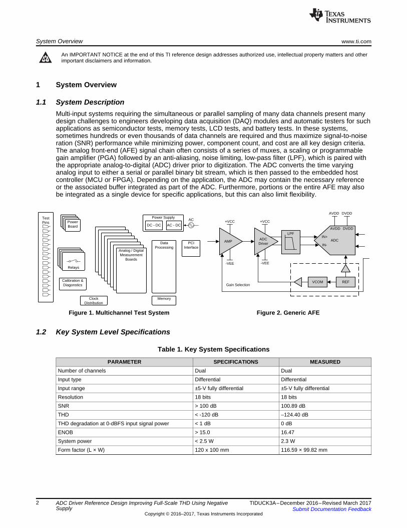
1.1 System DescriptionMulti-input systems requiring the simultaneous or parallel sampling of many data channels present manydesign challenges to engineers developing data acquisition (DAQ) modules and automatic testers for suchapplications as semiconductor tests, memory tests, LCD tests, and battery tests. In these systems,sometimes hundreds or even thousands of data channels are required and thus maximize signal-to-noiseration (SNR) performance while minimizing power, component count, and cost are all key design criteria.The analog front-end (AFE) signal chain often consists of a series of muxes, a scaling or programmablegain amplifier (PGA) followed by an anti-aliasing, noise limiting, low-pass filter (LPF), which is paired withthe appropriate analog-to-digital (ADC) driver prior to digitization. The ADC converts the time varyinganalog input to either a serial or parallel binary bit stream, which is then passed to the embedded hostcontroller (MCU or FPGA). Depending on the application, the ADC may contain the necessary referenceor the associated buffer integrated as part of the ADC. Furthermore, portions or the entire AFE may alsobe integrated as a single device for specific applications, but this can also limit flexibility.
Figure 1. Multichannel Test System Figure 2. Generic AFE
1.2 Key System Level Specifications
Table 1. Key System Specifications
PARAMETER SPECIFICATIONS MEASUREDNumber of channels Dual DualInput type Differential DifferentialInput range ±5-V fully differential ±5-V fully differentialResolution 18 bits 18 bitsSNR > 100 dB 100.89 dBTHD < -120 dB –124.40 dBTHD degradation at 0-dBFS input signal power < 1 dB 0 dBENOB > 15.0 16.47System power < 2.5 W 2.3 WForm factor (L × W) 120 x 100 mm 116.59 × 99.82 mm
LMK61E2OSC
PHI Connector
SN74AUP1G80
Flip-Flop
I2C
I2C
#CSSCLKSDI
SDO (0 ± 3)
RVS
CONVST
SYSCLK
24V DC
CONVST
#CSSCLK
SDISDO 0 - 3
(READY/CLK)RVS
18-Bit1 MSPS
SAR ADC
SMA Connector
VIN+
VIN-
REF6041Reference
4.096 V
EEPROM
DQ
IN+
IN-
+5 V
AVDD DVDD
VREF
_
_+
Vocm
Vocm
THS4551
OPA376
ADS8910B
-0.2 V
LMK00804BCLK DIST
TPS7A4700LDO
TPS7A4700LDO
18.5 V
18.0 V 5.3 V-0.2 V
SYSCLK
OPA827
18.0 V
-18.0 V
_
+
OPA827
18.0 V
-18.0 V
_
+
OPA625
5.0 V
-0.2 V
_
+
OPA6255.0 V
-0.2 V
_
+
CONVST
#CS
SCLK
SDI
SDO 0 - 3
(READY/CLK)RVS
18-Bit1 MSPS
SAR ADC
AVDDDVDD
VREF
VIN-
VIN+
SN74AUP1G80Flip-Flop
CONVST
SYSCLK
D
Q
PHI Connector
I2C
SYSCLK
#CS
SCLK
SDI
SDO (0 ± 3)RVS
SMA Connector
IN+
IN-
18.0 V
-18.0 V
_
+
OPA827
18.0 V
-18.0 V
_
+
3.3 V5.0 V
3.3 V
Vocm OPA
LM5574MTDC -DC
Buck/Boost
TPS7A3001LDO
-18.5 V
-18.0 V
ADS8910B
TPS7A4700LDO
3.8 V
3.3 V
Ideal External Supply
5.0 V
LM7705Negative
BiasGenerator
5.8 V
OPA827
Copyright © 2017, Texas Instruments Incorporated
www.ti.com System Overview
3TIDUCK3A–December 2016–Revised March 2017Submit Documentation Feedback
Copyright © 2016–2017, Texas Instruments Incorporated
ADC Driver Reference Design Improving Full-Scale THD Using NegativeSupply
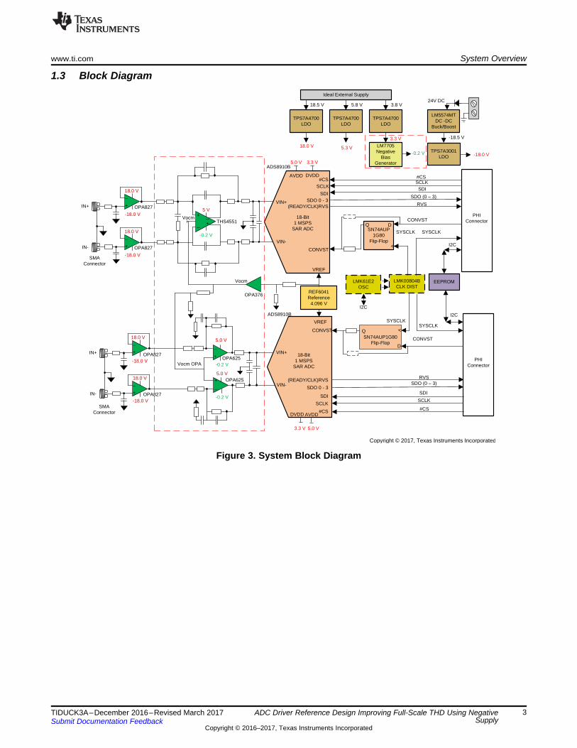
1.3 Block Diagram
Figure 3. System Block Diagram
+24 V Ideal External Supply
-18.5 V
-18 V
+18.5 V
+18 V
+5.5 V
+5 V
+3.8 V
+3.3 V -0.2 V
OPA827Buffers
Vref, OPA625's,THS4551,
ADC RVDD
ADC DVDD, Inverter,
Flip-Flops
System Overview www.ti.com
4 TIDUCK3A–December 2016–Revised March 2017Submit Documentation Feedback
Copyright © 2016–2017, Texas Instruments Incorporated
ADC Driver Reference Design Improving Full-Scale THD Using NegativeSupply
1.4 System Design TheoryThe complexity of automatic test equipment (ATE) systems continues to grow as their applicationdemands ever increasing input channels with some requiring more than 5000. In this reference design, amodular solution is proposed as to promote a design that will scale to the required number of inputs by theapplication. End equipment such as mixed signal SOC testers, memory testers, battery testers, LCDtesters, high density DAQ cards, high density power cards, x-ray inspection, and so on require multiple,simultaneous-sampling channels with excellent DC and AC performance, while managing power in orderto maximize PCB density. The AFE consists of the high-speed signal chain and the associated point-of-load (POL) power supplies it requires. This reference design explores the benefits of generating anadditional negative supply rail to provide the necessary headroom for the ADC driver amplifiers tomaintain the high level of signal linearity all the way to systems ground.
In order to optimize the different performance metrics of a modular multisampling ATE system, twodifferent front ends were used in this TI Design to compare the performance and application when used todrive identical high-performance successive approximation register (SAR) ADCs. One front-end uses afully differential amplifier (FDA) and the second uses two precision operational amplifiers (op amps). Theresulting digital data from the ADC output is connected to the Texas Instruments precision host interface(PHI, available for purchase with ADS8910B evaluation board) where the data is analyzed for SNR, THD,and other performance parameters.
The following sections detail the design challenges presented by high-channel count systems, includingtheory, calculations, component selection, simulations, PCB layout design, and measurement results.Unless otherwise noted, TI’s SPICE and design developments tools, TINA-TI™ and WEBENCH®, wereused to aid in development.
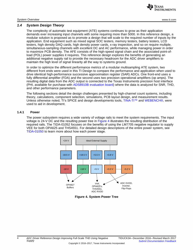
1.4.1 PowerThe power subsystem requires a wide variety of voltage rails to meet the system requirements. The inputvoltage is 24-V DC and the resulting power tree in Figure 4 illustrates the resulting distribution of therequired rails. The TIDA-01052 focuses on the benefits of using the LM7705 negative regulator to supplyVEE for both OPA625 and THS4551. For detailed design descriptions of the entire power system, seeTIDA-01050 to learn more about how each power stage.
Figure 4. System Power Tree

+
±
0 V
VIN +V
0 V
VOUT
VDSAT
Output Saturation
0 V+
V+
VDSAT
Input Voltage
Out
put V
olta
ge (
V)
CF+1
VSS5
VOUT6
CRES7
CF-8
VDD4
SD3
VSS2
U10
LM7705MM/NOPB
0.47µFC25
10µFC24
10µFC23
22µFC26
22µFC28
0.1µFC274.7µF
C290.22µFC30
0
R21
4.70
R22
GND GND GND GNDGND GND GND10µFC33
GND
GND-0.2V
3.3V
-0.2V Supply
Tp27
600 ohm
L4
600 ohm
L5
1
23
J34
TMM-103-01-G-S-SM
VEE
GND
Copyright © 2017, Texas Instruments Incorporated
www.ti.com System Overview
5TIDUCK3A–December 2016–Revised March 2017Submit Documentation Feedback
Copyright © 2016–2017, Texas Instruments Incorporated
ADC Driver Reference Design Improving Full-Scale THD Using NegativeSupply
1.4.1.1 –0.2-V Rail Design Theory
Figure 5. –0.2-V Rail Altium Schematic
To ensure the AFE can support a full voltage swing from 0 to VREF, a small –0.2-V rail (VEE) wasgenerated using the LM7705 as shown in Figure 5. Due to the architecture and transistor limitations, mostgeneral purpose amplifiers will saturate when the signal, at the input or output, nears the supply rails asillustrated in Figure 6. As the signal approaches this voltage, usually within few hundred millivolts of thesupply, many amplifier characteristics, such as linearity and supply rejection, start degrading.
Figure 6. Limitation of Output of an Amplifier
Amplifiers using "rail-to-rail" drive architectures do improve the overall dynamic range. For example, TI’sLMP7701 (a typical rail-to-rail op amp) has an output drive capability down to within 50 mV of VEE over alltemperatures for a 10-kΩ load resistance as shown in Figure 6. This is indeed close to the lower supplyvoltage rail; however, for applications requiring excellent linearity to system ground (0 V), this can stillimpact signal chain performance and reduce the effective number of bits (ENOB). This is illustrated inFigure 7.
Figure 7. Output Limitation for Single-Supply True Zero Output Application

Power Supply
Pre Regulator
Charge Pump
Post Regulator
Load
LM7705
Copyright © 2017, Texas Instruments Incorporated
+
±
0 V
VIN +V
0 V
VOUT
-V
System Overview www.ti.com
6 TIDUCK3A–December 2016–Revised March 2017Submit Documentation Feedback
Copyright © 2016–2017, Texas Instruments Incorporated
ADC Driver Reference Design Improving Full-Scale THD Using NegativeSupply
The limitations of the output stage of the op amp can be omitted by using a dual-supply op amp and anegative regulator to enable to the op amp to support full scale signal swing. By lowering the supply railbelow ground, the op amp is now able to use the full-scale range of the ADC without sacrificing linearity.Figure 8 shows the output drive of an amplifier in a true zero output voltage application.
Figure 8. Amplifier Output Drive With a Dual Supply
Traditional dual supply disadvantages:• Adding a second regulator to generate the negative supply adds additional cost.• The negative voltage generated by the second supply may exceed the voltage limitations of the
desired op amp and thus a different device or a more complex design solution is required.
With an enhanced solution using TI’s LM7705 low-noise negative bias generator:• The design operates with only a single positive supply, reducing cost.• The LM7705 generates a negative supply voltage of only –0.23 V, which is than enough to enable a
full-scale signal path.• In most applications, this small extension of the supply voltage range is usually within the operating
range of most op amps and a full redesign is not necessary.
The main function of the LM7705 is to supply a stabilized negative bias voltage to a load, using only apositive supply voltage. A general block diagram for this charge pump inverter is given in Figure 9. Theexternal power supply and load are added in this diagram as well.
Figure 9. LM7705 Architecture
The LM7705 low-noise negative bias generator can be used for many applications requiring full scalesignal swing. Simply connecting the LM7705 between the positive (3 to 5.25 V) supply, it will provide asmall negative voltage (–0.23 V) that does not exceed the maximum supply voltage ratings of the most opamps. In this system, traces for –0.2 V and ground were placed on the negative supply pins of the opamps. The two different rails are selectable through the jumper J34.

ADC
REFP
BufferVoltage
Reference
RREF_FLT
CBUF_FLT
RBUF_FLT
CBUF_FLT
Copyright © 2017, Texas Instruments Incorporated
Oscillator
V+ S1
S2
CAP+ S3
CFLY
S4
CAP-
Ø1 Ø2
OUT = V-
CRES
Copyright © 2017, Texas Instruments Incorporated
www.ti.com System Overview
7TIDUCK3A–December 2016–Revised March 2017Submit Documentation Feedback
Copyright © 2016–2017, Texas Instruments Incorporated
ADC Driver Reference Design Improving Full-Scale THD Using NegativeSupply
The voltage inversion in the LM7705 is achieved using a switched capacitor technique with two externalcapacitors (CFLY and CRES). An internal oscillator and a switching network transfers charge between thetwo storage capacitors. This switched capacitor technique is given in Figure 10.
Figure 10. Voltage Inverter
The internal oscillator generates two anti-phase clock signals. Clock 1 controls switches S1 and S2. Clock2 controls switches S3 and S4. When switches S1 and S2 are closed, capacitor CFLY is charged to V +.When switches S3 and S4 are closed (S1 and S2 are open), charge from CFLY is transferred to CRESand the output voltage OUT is equal to –V +.
Due to the switched capacitor technique, a small ripple will be present at the output voltage with afrequency of the oscillator. The magnitude of this ripple increases with output currents. The magnitude ofthe ripple can be influenced by changing the values of the used capacitors.
The LM7705 has a 4-mVPP output voltage ripple at 92 kHz. To ensure that this will not cause any noiseissues within the system, the noise seen by the ADC can be computed using the PSRR specification ofthe amplifiers. The OPA625 has a PSRR of –70 dB at 90 kHz and the THS4551 has a PSRR of –110 dBat 90 kHz. To compute the worst case scenario, the OPA625's specification is used for the calculations.–70 dB is equivalent to a voltage gain of 0.000316 V/V. Multiplying 4 mVPP by the PSRR of the OPA625results in a 1.26-µVPP noise present at the ADC input caused by the LM7705. Considering the inputvoltage to be 5 VPP, a 1.26-µVPP noise results in a noise signal of –132 dBc, which is in line with thenoise floor of the system. Therefore, the ripple caused by the LM7705 is effectively too small to affect theADC’s performance.
For more detailed information, see the LM7705 datasheet.
1.4.1.2 Reference Voltage Design TheoryExternal voltage reference circuits are used in a DAQ system if there is no internal reference in the ADCor if the accuracy of the internal reference is not sufficient to meet the performance goals of the system.These circuits must provide a low-drift, low-noise, and accurate voltage for the ADC reference input.However, the output broadband noise of most references can be in the order of a few 100 µVRMS, whichdegrades the noise and linearity performance of precision ADCs, for which the typical noise is in the orderof tens of µVRMS. So, to optimize the ADC performance, the output of the voltage reference must beappropriately filtered and buffered.
Figure 11. Simplified Schematic of Reference Driver Circuit

Common Mode Voltage
AGND
1µFC321
AGND
1
2
3
4
5
U4OPA376AIDBVR
1µF
C31920.0k
R216
499
R215
5V
0.1µF
C320
AGND
AGND
1µFC318
49.9kR217
49.9k
R218
AGND
499
R214
V_CM_OPAVref
TP28TP29
V_CM
Copyright © 2017, Texas Instruments Incorporated
0.22R4
AGND
0.22R3
AGND
1µFC4
AGND
10µFC3
5V
AGND
Vref
Reference Voltage (5.0V)
0R255
DNPVref147µF
C5
VIN1
SS3
FILT4
EN2
OUT_S5
OUT_F6
GND_F7
GND_S8
U3
REF6050IDGKR
Copyright © 2017, Texas Instruments Incorporated
BufferBandgap Voltage
Reference+
VIN
SS
-
VIN
RFLT
EN
GND_S FILT GND_F
OUT_F
OUT_S
Copyright © 2017, Texas Instruments Incorporated
System Overview www.ti.com
8 TIDUCK3A–December 2016–Revised March 2017Submit Documentation Feedback
Copyright © 2016–2017, Texas Instruments Incorporated
ADC Driver Reference Design Improving Full-Scale THD Using NegativeSupply
Most SAR ADCs, and a few delta-sigma ADCs, switch binary-weighted capacitors onto the REF pin duringthe conversion process. The magnitude of the capacitance switched onto the REF pin during eachconversion depends on the input signal to the ADC. If a voltage reference is directly connected to the REFpin of these ADCs, the reference voltage droops because of the dynamic input signal dependent load ofthe binary-weighted capacitors. Because the reference voltage droop now has input signal dependence,the THD and linearity for the system degrades significantly.
In order to support this dynamic load and preserve the ADC linearity, distortion and noise performance,the output of the voltage reference must be buffered with a low-output impedance (high-bandwidth) buffer.The REF60xx family of voltage references has an integrated low-output impedance buffer that enables theuser to directly drive the REF pin of an SAR ADC, while preserving ADC linearity and distortion. Inaddition, the total noise in the full bandwidth of the REF60xx is extremely low, thus preserving the noiseperformance of the ADC.
Figure 12. REF60xx Functional Block Diagram
The output voltage of the REF60xx does not droop below 1 LSB (18 bits), even during the first conversionwhile driving the REF pin of the ADS8910B. This feature is extremely useful in burst-mode, event-triggered, equivalent-time sampling, and variable-sampling-rate DAQ systems.
Figure 13. Reference Voltage Altium Schematic
1.4.1.3 Common-Mode Voltage Design Theory
Figure 14. Common-Mode Voltage Altium Schematic

refV
2
g
f g
R
R R+
f
g
R1
R+
www.ti.com System Overview
9TIDUCK3A–December 2016–Revised March 2017Submit Documentation Feedback
Copyright © 2016–2017, Texas Instruments Incorporated
ADC Driver Reference Design Improving Full-Scale THD Using NegativeSupply
The common-mode voltage is the voltage the THS4551 and the OPA625 driver amplifiers center theoutput signal around. To enable full signal swing, the common-mode voltage should be exactly half thereference voltage. To achieve this, the OPA376 is used with a resistor divider on the input to divide thereference voltage in half. The OPA376 is buffering the voltage from the resistor divider to the load.
For the single-ended OPA625 ADC drivers, the output common-mode is set by applying the input
common-mode voltage at the non-inverting terminal. There is a gain from the non-inverting input to
the output. Due to this gain, the input voltage needed to be scaled down by a factor of . Thiswas implemented with R214, and R110 + R111.
C320, C321, and C318 in Figure 14 are used as decoupling capacitors to help reduce any noise on theserails. Components R216, C319, and R215 are placed to ensure the stability of the circuit.
Figure 15. OPA376 Stability Simulation Circuit
TINA-TI was used to model this circuit. The simulation schematic is shown in Figure 15. The theory forcompleting stability simulations are covered in TI’s Precision Labs lectures on op amps
Figure 16. OPA376 Stability Simulation Results
28 V/μs2.52 MHz
2.52
2
=
p ´
P
SRf
V2
2
=
p
PV SR
2 f2=
p
3
2
6
74
V+
V- OPAN_1AOPA827AIDR
+18V
-18V
AGND
AGND
0.1µF
C79
0.1µF
C80
Copyright © 2017, Texas Instruments Incorporated
System Overview www.ti.com
10 TIDUCK3A–December 2016–Revised March 2017Submit Documentation Feedback
Copyright © 2016–2017, Texas Instruments Incorporated
ADC Driver Reference Design Improving Full-Scale THD Using NegativeSupply
The results from the TINA-TI simulations are shown in Figure 16. The loaded open loop gain curveintersects with the noise gain curve with a rate of closure less than 40 dB/decade. This is indicative of astable circuit. Furthermore, the phase margin is 70.96⁰, which is well above the 45⁰ threshold required fora stable circuit.
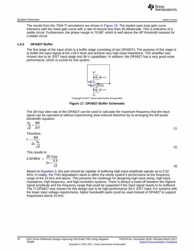
1.4.2 OPA827 BufferThe first stage of the input chain is a buffer stage consisting of two OPA827s. The purpose of this stage isto buffer the input signal at the ±18-V level and achieve very high-input impedance. This amplifier waschosen due to its JFET input stage and 36-V capabilities. In addition, the OPA827 has a very good noiseperformance, which is crucial for this system.
Figure 17. OPA827 Buffer Schematic
The 28-V/µs slew rate of the OPA827 can be used to calculate the maximum frequency that the inputsignal can be operated at without experiencing slew-induced distortion by re-arranging the full powerbandwidth equation.
(1)
Therefore,
(2)
This results in:
(3)
Based on Equation 3, this part should be capable of buffering high-input amplitude signals up to 2.52MHz; in reality, the THD degradation starts to affect the whole system’s performance at the frequencyrange of the 10 kHz and above. This presents the challenge for designing high-input swing, high-inputimpedance, high frequency, and high-resolution systems. There is always a trade-off between the highestsignal amplitude and the frequency range that could be supported if the input signal needs to be buffered.The TI OPA827 was chosen for this design due to its high-performance 36-V JFET input. For systems withthe lower input voltage requirements, higher bandwidth parts could be used instead of OPA827 to supportfrequencies above 10 kHz.

www.ti.com System Overview
11TIDUCK3A–December 2016–Revised March 2017Submit Documentation Feedback
Copyright © 2016–2017, Texas Instruments Incorporated
ADC Driver Reference Design Improving Full-Scale THD Using NegativeSupply
Figure 18. OPA827 TINA-TI Stability Schematic
Figure 18 highlights the schematic used to test the stability of the OPA827 buffer stage. When measuringthe stability of an amplifier, it is important to look at the closed-loop noise gain, loaded open-loop gain, andloop gain. The phase margin of the circuit also needs to be sufficient for circuit stability and requiredsettling. See TI’s Precision Labs for more details on op amp design and amplifier stability.
In The TINA-TI schematic in Figure 18 features a 1TF capacitor and 1TH inductor for simulation purposes.This is used to break the feedback loop as the capacitor will be an open at DC while the inductor is ashort. At high frequencies, the inductor will be an open and the capacitor will be a short. The load theOPA827 will see by the next stage of the system was also added on the right side of the schematic. Thisallows for the proper simulation of the circuits stability.
Figure 19. OPA827 TINA-TI Stability Simulation Results
Figure 19 highlights the results from the OPA827 stability simulation resulting in a phase margin of >73⁰implying stability. It is also important to consider the rate of closure between the loop gain and loadedopen loop gain curves. The loaded open loop gain is decreasing at –20 dB/decade at the point ofintersection with the noise gain curve. The noise gain curve is flat, meaning it is at 0 dB/decade. The rateof closure is thus 20 dB/decade. For a circuit to be considered stable, the rate of closure has to be lessthan 40 dB/decade. For more information about amplifier stability, see TI’s Precision Labs.

System Overview www.ti.com
12 TIDUCK3A–December 2016–Revised March 2017Submit Documentation Feedback
Copyright © 2016–2017, Texas Instruments Incorporated
ADC Driver Reference Design Improving Full-Scale THD Using NegativeSupply
To further confirm the functionality of the OPA827 buffer stage, transient simulations were completed toensure the response is appropriate. Figure 20 illustrates the schematic used in TINA-TI to simulate thetransient response of the OPA827 buffer stage. When simulating the transient response of an amplifier, itis important to input a signal with a sharp edge. In this simulation, a 50-mV amplitude, 50-kHz squarewave is applied to the input and the output response is observed over a 100-µs period.
Figure 20. TINA-TI Transient Schematic Figure 21. TINA-TI Transient Simulation
Figure 21 illustrates the results of the transient simulation. The output of the OPA827 buffer shows noringing and only a slight slew limitation at the beginning and the end of each rising/falling edge. Fromthese results, it is concluded that the OPA827 buffer is stable and will perform as expected.
In Figure 20, 0.1-µF decoupling capacitors are placed on both the positive and negative supplies of theOPA827. This is to help remove any noise present on the power supplies. This value is recommended inSection 7 of the OPA827 datasheet.
1.4.3 THS4551 DriverThe input driver circuit for a high-precision ADC mainly consists of two parts: a driving amplifier and aflywheel RC filter. The amplifier is used for signal conditioning of the input signal, and its low-outputimpedance provides a buffer between the signal source and the ADC’s switched capacitor inputs. The RCfilter helps attenuate the sampling charge injection from the switched capacitor input stage of the ADC andfunctions as an anti-aliasing filter to band-limit the wideband noise contributed by the front-end circuit.Careful front-end circuit design is required to meet the resolution, linearity, and noise performancecapabilities of the ADS8910B. The input op amp must support following key specifications:1. Rail-to-rail input and output (RRIO)2. Low noise3. High small-signal bandwidth with low distortion at high frequencies4. Low power
For DC signals with fast transients that are common in a multiplexed application, the input signal mustsettle within an 18-bit accuracy at the device inputs during the acquisition time window. This condition iscritical to maintain the overall linearity performance of the ADC. Typically, the amplifier datasheets specifythe output settling performance only up to 0.1% to 0.001%, which may not be sufficient for the desired 18-bit accuracy. Therefore, it is required to verify the settling behavior of the input driver within the simulatorssuch as TINA-TI to help select the appropriate amplifier.

AINP
AINM
Device
GNDC FLT 900 pF
C FLT 900 pF
R FLT 10
R FLT 10
Copyright © 2017, Texas Instruments Incorporated
3dB
FLT FLT
1f
2 R C-
=
p ´ ´
www.ti.com System Overview
13TIDUCK3A–December 2016–Revised March 2017Submit Documentation Feedback
Copyright © 2016–2017, Texas Instruments Incorporated
ADC Driver Reference Design Improving Full-Scale THD Using NegativeSupply
Converting analog-to-digital signals requires sampling an input signal at a constant rate. Any higherfrequency content in the input signal beyond half the sampling frequency is digitized and folded back intothe low-frequency spectrum of interest known as aliasing. Therefore, an analog antialiasing filter must beused to remove the noise and harmonic content from the input signal before being sampled by the ADC.An anti-aliasing filter is designed as a low-pass RC filter, where the 3-dB bandwidth is optimized based onspecific application requirements.
For DC signals with fast transients (including multiplexed input signals), a high-bandwidth filter is designedto allow accurate settling of the signal at the inputs of the ADC during the small acquisition time window.
For AC signals, keeping the filter bandwidth low is desirable to band-limit the noise fed into the input of theADC, thereby increasing the system SNR. Besides filtering the noise from the front-end drive circuitry, thefilter also helps attenuate the sampling charge injection from the switched-capacitor input stage of theADC. A filter capacitor, CFLT, is connected from each input pin of the ADC to the ground (as shown inEquation 4 and Figure 22).
This capacitor helps reduce the sampling charge injection and provides a charge bucket to quickly chargethe internal sample-and-hold capacitors during the acquisition process. Generally, the value of thiscapacitor must be at least 15 times the specified value of the ADC sampling capacitance. For theADS8910B, it is recommended to keep CFLT greater than 900 pF. The capacitor must be a COG- or NPO-type because these capacitor types have a high-Q, low-temperature coefficient, and stable electricalcharacteristics under varying voltages, frequency, and time.
(4)
Figure 22. Anti-Aliasing Filter Configuration Diagram
Note that driving capacitive loads can degrade the phase margin of the input amplifiers, thus making theamplifier marginally unstable. To avoid amplifier stability issues, series isolation resistors (RFLT or RISO) areused at the output of the amplifiers. A higher value of RFLT is helpful from the amplifier stability perspective,but adds distortion as a result of interactions with the nonlinear input impedance of the ADC. Distortionincreases with source impedance, input signal frequency, and input signal amplitude. Therefore, theselection of RFLT requires balancing the stability and distortion of the design. For the ADS8910B, limitingthe value of RFLT to a maximum of 10 Ω is recommended to avoid any significant degradation in linearityperformance. The tolerance of the selected resistors must be kept less than 1% to keep the inputsbalanced. The driver amplifier must be selected such that its closed-loop output impedance is at least fivetimes lesser than the RFLT.
Following the OPA827 is the THS4551 for one of the ADC drivers. The THS4551 is a fully differentialamplifier specifically designed to be used with high performance SAR ADCs. The gain of this stage isconfigured to be 1. RDP1 and RDP2 in Figure 23 are connected in series to give 1 kΩ while R101 is also1 kΩ. RDN1, RDN2, and R101 deliver the same gain for the negative input to the fully differentialamplifier. Additionally, C87, C86, R211, R212, R103, R104, C89, C90, and C315 were added to ensurestability. The selection of these components is discussed in TIDA-01050. R211 and R212 are 0-Ωplaceholder resistors for later study (for example, in case larger isolation is required). Capacitors C89,C90, and C315 are flywheel or "charge bucket" capacitors designed to quickly charge the sample and holdcircuit inside the ADC. It is important to place the single-ended capacitors C89 and C90 from each ADCinput to GND in addition to the differential capacitor C315 to ensure the common-mode voltage is stableduring the switching of the sample and hold circuit.

249R99
DNP
68pFC83DNP AGND
AGND
IN-3
OUT+10
FB+4
VOCM9
OUT-11
IN+2
FB-1
PD12
VS
+7
VS
+6
VS
+5
VS
+8
VS
-13
VS
-14
VS
-15
VS
-16
EP17
FDA1
THS4551IRGTR
V_CM
0.1µF
C84
AGND
0R212
0R211
VEE0
R248
0.1µF
C317
DNP
0.1µF
C316
DNP
5V
0.1µF
C85
AGND
10µF
C284
AGND
5V
AGND
0.01µFC315
1000pFC89
1000pFC90
4.42
R103
4.42
R104
1.00k
RDP2
0
RDP1
1.00k
RDN2
0
RDN1
1.00k
R100
1.00k
R101
1000pF
C86
1000pF
C87
Copyright © 2017, Texas Instruments Incorporated
System Overview www.ti.com
14 TIDUCK3A–December 2016–Revised March 2017Submit Documentation Feedback
Copyright © 2016–2017, Texas Instruments Incorporated
ADC Driver Reference Design Improving Full-Scale THD Using NegativeSupply
Figure 23. THS4551 Stage Altium Schematic
Figure 23 shows that the power down pin (pin 12) of the THS4551 is connected to 5 V. The power downpin is logic low, meaning that when it is grounded, the chip is in power off mode. When this pin is high, it isin normal operation mode. For this application, the amplifier will always be in normal operation mode. Pin17 is the thermal pad and is connected to ground to ensure that the chip has a proper heat sink. Thevoltage driven at the common-mode voltage pin is 2.5 V.
1.4.4 Dual OPA625 DriverThe OPA625 is designed to drive precision (up to 18 bits) SAR ADCs at sample rates up to 2 MSPS. Thecombination of low output impedance (1 Ω at 1 MHz), low THD, low noise (2.5 nV/√Hz), and fast settlingtime (4-V step, 16-bit levels within 280 ns) make the OPA625 the ideal choice for driving both the SARADC inputs as well as the reference input to the ADC.
AGND
V_CM_OPA
1000pFC109
AGND
1000pFC115
AGND
5V
5V
VEE
VEE
470pF
C110
DNP
470pF
C113
DNP
30.0R113
DNP
30.0R112
DNP
AGND
AGND
AGND
AGND
3
1
2
4
6
5
V+
V-U2
OPA625IDBVR
3
1
2
4
6
5
V+
V-U1
OPA625IDBVR
0.1µFC112
0.1µFC116
AGND
AGND
0.1µF
C108
AGND
10µF
C304
AGND
10µF
C305
AGND
0R213
TP30
0R250
0R252
V_ref_OPA0
V_ref_OPA1
V_ref_OPA0 V_ref_OPA1
0.01µFC335
1.00k
R114
1000pF
C111
1.00k
R1161000pF
C1141.00kR110
1.00k
RDN4
1.00k
RDP4
0
RDP3
0
RDN3
2.2
R115
2.2
R117
0R111
0.01µFC118
0.01µFC117
Copyright © 2017, Texas Instruments Incorporated
www.ti.com System Overview
15TIDUCK3A–December 2016–Revised March 2017Submit Documentation Feedback
Copyright © 2016–2017, Texas Instruments Incorporated
ADC Driver Reference Design Improving Full-Scale THD Using NegativeSupply
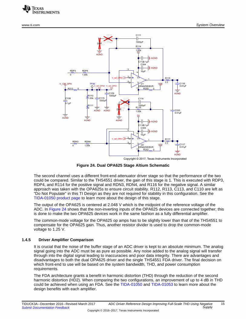
Figure 24. Dual OPA625 Stage Altium Schematic
The second channel uses a different front-end attenuator driver stage so that the performance of the twocould be compared. Similar to the THS4551 driver, the gain of this stage is 1. This is executed with RDP3,RDP4, and R114 for the positive signal and RDN3, RDN4, and R116 for the negative signal. A similarapproach was taken with the OPA625s to ensure circuit stability. R112, R113, C113, and C110 are left as"Do Not Populate" in this TI Design as they are not required for stability in this configuration. See theTIDA-01050 product page to learn more about the design of this stage.
The output of the OPA625 is centered at 2.048 V which is the midpoint of the reference voltage of theADC. In Figure 24 shows that the non-inverting inputs of the OPA625 devices are connected together; thisis done to make the two OPA625 devices work in the same fashion as a fully differential amplifier.
The common-mode voltage for the OPA625 op amps has to be slightly lower than that of the THS4551 tocompensate for the OPA625 gain. Thus, another resistor divider is used to drop the common-modevoltage to 1.25 V.
1.4.5 Driver Amplifier ComparisonIt is crucial that the noise of the buffer stage of an ADC driver is kept to an absolute minimum. The analogsignal going into the ADC must be as pure as possible. Any noise added to the analog signal will transferthrough into the digital signal leading to inaccuracies and poor data integrity. There are advantages anddisadvantages to both the dual OPA625 driver and the single THS4551 FDA driver. The final decision onwhich front-end to use will be based on the system bandwidth, THD, and power consumptionrequirements.
The FDA architecture grants a benefit in harmonic distortion (THD) through the reduction of the secondharmonic distortion (HD2). When comparing the two configurations, an improvement of up to 4 dB in THDcould be achieved when using an FDA. See the TIDA-01050 and TIDA-01053 to learn more about thedesign benefits with each amplifier.

SDO-218
CONVST 1
RST 2
DVDD16
REFM4 SDO-3 17
REFBUFOUT5
NC6
DECAP14
GND 15
DECAP13
REFIN3
EP25
SDO-119
SDO-0 20
RVS 21SDI 22
SCLK23
CS24
REFP7
REFM8
AINP9AINM10
RVDD12
GND 11
UADS1
ADS8910BIRGER
AGND
AGND
REFBUF_DIF
AGND
GND
NC 1
A2
GND3
Y4
VCC 5
U19
SN74AHC1G04DBVR
3.3V
GND
0.1µF
C95
GND
TP1
0.1µFC91
0.1µFC92
AGNDAGND
0.1µFC93
AGND
CONVSTn_DIF
10µF
C291
10µFC288
AGND
10µFC287
AGND
10µFC289
AGND
CONVST_To_DIF_ADC
22µFC322
0R2350R2340R2330R232
1µFC88
10.0k
R258
0
R260
0
R259Vref
Vref11.00R268
AGND
600 ohmL8
600 ohmL9
D 1
CLK 2
GND3
Q4
VCC5
U18
SN74AUP1G80DCKR
3.3V
0.1µF
C94
GND
10µF
C290
TP2
TP7
3.3V5V
SDO0_DIF
SDO1_DIF
SDO2_DIF
SDO3_DIF
RVS_DIF
SCLK
CSn
SRESETn
SDI
SYSCLK0
CONVST
CONVST
0R284
1
2
3
J33
TMM-103-01-G-S-SM
Copyright © 2016, Texas Instruments Incorporated
System Overview www.ti.com
16 TIDUCK3A–December 2016–Revised March 2017Submit Documentation Feedback
Copyright © 2016–2017, Texas Instruments Incorporated
ADC Driver Reference Design Improving Full-Scale THD Using NegativeSupply
1.4.6 ADS8910B ADC and Conversion Start Sync
Figure 25. ADS8910B and CONVST Sync Stage Altium Schematic
Two ADS8910B high-speed SAR ADCs are used to convert data from an analog to a digital signal. TheADC is directly following either the THS4551 fully differential amplifier driver stage or the two OPA625sconfigured as a differential amplifier driver stage. The outputs of the driver stages are directly fed into theAINP and AINM pins on the ADS8910B. The ADS8910B is powered by both 5 and 3.3 V. RVDD is theanalog supply and DVDD is the digital supply. As seen in Figure 25, ferrite beads are placed in betweenthe voltage input pins and the voltage rails to help filter any noise on the power supply rails. C287, C288,C91, and C92 are also added as decoupling capacitors to further help with the filtering of the powersupply. For the DECAP pins (pin 13 and pin 14), a decoupling capacitor is placed here with the two pinsshorted together. This implementation is described in Section 5 of the ADS8910B datasheet. The DECAPand REFP/REFBUFOUT pins are also configured as recommended by the datasheet. The 1-Ω resistor isadded as a place holder in case the impedance of the reference buffer capacitor needed to be adjusted.Pins 4 and 8, or the REFM pins were shorted together and attached to ground. These pins are thereference voltages ground potential and must be connected to ground for this application. Pin 3 is ananalog input for the reference voltage; the reference voltage is generated externally to the ADC and isdiscussed in further detail in Section 1.4.1.2. As seen in Figure 25, two different reference voltage nodeswere attached to this pin using 0-Ω resistors as placeholders to select between the two options. This isdone as one of the traces on the PCB would be made much longer to observe the potential losses and theeffect that has on the accuracy of the ADC. R258, C289, and C93 were used as a low-pass filter toremove any potential high-frequency noise on the reference voltage. Pins 11 and 15 are the ground pinsof the ADC and were connected to the systems ground. Pin 25 is the enable pin of the ADC; it isconnected to ground to make sure the chip is always enabled.
The SDO pins of the ADC (pins 17 to 20) were connected using 0 Ω directly towards the correspondingPHI connector where the performance of this ADC is analyzed. The RVS pin of the ADC also goes directlyto the corresponding PHI connector.
The SDI pin on the ADC (pin 22) is connected to the SDI of the PHI connector board. This makes it sothat the ADC is controlled by the FPGA on the PHI board. The SDI pin, or the serial data input pin, is usedto feed data or commands into the device. The FPGA on the PHI board is generating the SDI signal. Bothof the ADCs are connected to the same SDI signal, since only one ADC would be tested at a time, nointerference would be generated by doing this. The SCLK pin (pin 23) is the clock input pin for the serialinterface. All system-synchronous data transfer protocols are timed with respect to the SCLK signal. Asseen in Figure 25, SCLK is coming directly from the PHI connectors. The chip-select pin is active low andrequires a low input for the device to take control of the data bus. The reset pin (pin 2) is also connectedto the PHI connector in the same manner as the SDI signal is. Just like with the SDI signal, both ADCs areconnected to the same reset signal. A low pulse on the reset pin resets the device. All register bits willthen return to the default state.

OE1
ADD 2
GND 3
SCL8
OUTP4
OUTN5
VDD6
SDA7
U15
LMK61E2-SIAR
3.3V
GND
0.1µF
C61
10µF
C62
GND
4.7kR88
4.7kR89
0.1µF
C63
0.1µF
C64
100R92
4.7kR90
3.3V
4.7kR91
SCL
SDA
BCLK0_P
BCLK0_N
Copyright © 2017, Texas Instruments Incorporated
www.ti.com System Overview
17TIDUCK3A–December 2016–Revised March 2017Submit Documentation Feedback
Copyright © 2016–2017, Texas Instruments Incorporated
ADC Driver Reference Design Improving Full-Scale THD Using NegativeSupply
Table 2. SN74AUP1G80 Function Table
INPUTS OUTPUTQCLK D
↑↑
L or H
HLX
LHQ0
As seen in Figure 25, a unique approach is taken with the conversion start signal. Pin 1 on the ADC,CONVST, is used to start the ADC conversion. However, the CONVST signal needs to be synchronizedwith the SYSCLK signal to ensure proper data integrity. To achieve this, an inverter and a D flip-flop areused to synchronize the conversion start signal coming from the precision host interface (PHI) connectorto the SYSCLK signal generated by the clock circuit. The CLK input to the flip-flop is the SYSCLK signalthat is consistent throughout the system. Decoupling capacitors of 1 µF and 10 µF were used on both theflip flop and inverter. J33 in Figure 25 was placed so that the unsynchronized conversion start signal couldbe used if wanted.
To ensure the best results, onboard clocking was implemented. When maximizing system performance,clock jitter must be kept to an absolute minimum. TI’s PHI is an external device. Clock jitter can be addedto the system through the connection between the PHI and the TIDA-01052 board. This is prevented byusing on board clocking and the onboard CONVST and SYSCLK synchronization.
1.4.7 ClockingThe PHI is used to analyze ADC performance; however, the connection between the external PHI boardand the system adds jitter. The LMK61E2 was used as the internal master clock in order to minimize thejitter effects. The LMK61E2 is an ultra-low jitter PLLatinum™ programmable oscillator with a fractional-Nfrequency synthesizer with integrated VCO that generates commonly used reference clocks. The outputscan be configured as LVPECL or LVDS or HCSL. The device features self-startup from on-chip EEPROMthat is factory programmed to generate 156.25 MHz LVPECL output. The device registers and EEPROMsettings are fully programmable in system through I2C serial interface. Internal power conditioning provideexcellent power supply ripple rejection (PSRR), reducing the cost and complexity of the power deliverynetwork. The device operates from a single 3.3-V ± 5% supply. The device provides fine and coarsefrequency margining options through I2C serial interface to support system design verification tests (DVT)such as standard compliance and system timing margin testing.
Figure 26. LMK61E2 Altium Schematic
As seen in Figure 26, pins 7 and 8 are connected to an external USB2ANY header (J3). SDA and SCLare used for the I2C serial interface. The USB2ANY header is used to connect an external I2Cprogrammer. Both pins require an external pull up resistor to VCC.
VDD is connected to 3.3 V and two decoupling capacitors are used. For best electrical performance of theLMK61E2 device, use a combination of 10 µF, 1 µF, and 0.1 µF on its power supply bypass network. It isalso recommended to use component side mounting of the power supply bypass capacitors, and it is bestto use 0201 or 0402 body size capacitors to facilitate signal routing. Keep the connections between thebypass capacitors and the power supply on the device as short as possible. Ground the other side of thecapacitor using a low-impedance connection to the ground plane. The output enable pin of the LMK61E2is also connected to VDD; this allows the output to always be enabled.

System Overview www.ti.com
18 TIDUCK3A–December 2016–Revised March 2017Submit Documentation Feedback
Copyright © 2016–2017, Texas Instruments Incorporated
ADC Driver Reference Design Improving Full-Scale THD Using NegativeSupply
Figure 27. LMK61E2 Functional Block Diagram
Pin 2 on the LMK61E2 is another digital control interface pin. When left open, LSB of I2C slave address isset to "01". When tied to VDD, LSB of I2C slave address is set to "10". When tied to GND, LSB of I2Cslave address is set to "00". As seen in Figure 26, ADD can be connected to either VCC or GND throughthe configuration of the two 4.7-kΩ resistors. The default configuration is to connect ADD to VCC.
The clock generator is configured to output a 65-MHz frequency clock signal across pins 5 and 4 of thedevice. These two pins comprise an LVDS signal that is then passed through a 0.1-µF capacitor andterminated with a 100-Ω resistor.

Q0
Q1
Q2
Q3
RPU
OE
RPU = PullupRPD = Pulldown
0
1
QDRPU
RPD
RPD
RPD
RPU
RPU
CLK_EN
LVCMOS_CLK
CLK
nCLK
CLK_SEL
Copyright © 2017, Texas Instruments Incorporated
100R92
33
R95
33
R256
33
R257
3.3V
0.1µFC340
GNDGNDGND
10µFC338
600 ohm
L10
1µFC339
TP16
TP31
TP32
SYSCLK0
SYSCLK1
SYSCLK2
SYSCLK3
GND1
OE2
VDDO11
VDD3
CLK_EN4
CLK5
nCLK6
CLK_SEL7
LVCMOS_CLK8 GND 9
Q3 10
Q212
GND13
VDDO15
Q1 14
Q016
U33
LMK00804BPW
GND
GND
GND
3.3V
0.1µF
C349
GNDGNDGND
10µF
C347600 ohm
L12
1µF
C348
VDD
VDDO
VDD
VDD
VDDO
VDDO
33
R278
BCLK1_P
BCLK1_N
0.1µF
C350
GND
TP33
Copyright © 2017, Texas Instruments Incorporated
www.ti.com System Overview
19TIDUCK3A–December 2016–Revised March 2017Submit Documentation Feedback
Copyright © 2016–2017, Texas Instruments Incorporated
ADC Driver Reference Design Improving Full-Scale THD Using NegativeSupply
Figure 28. LMK00804BPW Clock Distributor Altium Schematic
The LMK61E2 outputs one LVDS clock signal; however, the system requires SYSCLK to go to multipledifferent locations. Each of these locations only accepts an LVCMOS clock signal. To handle thisrequirement, an LMK00804BPW is used. The LMK00804 is a clock fan-out buffer, which distributes fourLVCMOS clocks. The LMK00804 is configured to accept a differential input clock and distribute it to fourLVCMOS clocks that are all synchronized.
The CLKSEL pin (pin 7) is used to configure what type of input clock is used. In this system, an LVDSclock was generated from the LMK61E2 so the LMK00804 needed to be configured accepts an LVDSclock. This is done by connecting pin 7 to VDD. If pin 7 is grounded, an LVCMOS clock can be input.
Figure 29. LMK00804BPW Functional Block Diagram

+
± OPA625
5 V
Mode Control
VREF / 4
Input Voltage
1 N1 N
4.7
4.7 10 nF ADS8860
GND
VREF 3.3 V
Copyright © 2017, Texas Instruments Incorporated
System Overview www.ti.com
20 TIDUCK3A–December 2016–Revised March 2017Submit Documentation Feedback
Copyright © 2016–2017, Texas Instruments Incorporated
ADC Driver Reference Design Improving Full-Scale THD Using NegativeSupply
The LMK00804B is a low-skew, high-performance clock fan-out buffer which can distribute up to fourLVCMOS or LVTTL outputs (3.3-V, 2.5-V, 1.8-V, or 1.5-V levels) from one of two selectable inputs, whichcan accept differential or single-ended inputs. The clock enable input is synchronized internally toeliminate runt or glitch pulses on the outputs when the clock enable terminal is asserted or de-asserted.The outputs are held in a logic low state when the clock is disabled. A separate output enable terminalcontrols whether the outputs are active state or high-impedance state. The low additive jitter, phase noisefloor, guaranteed output, and part-to-part skew characteristics make the LMK00804B ideal for applicationsdemanding high performance and repeatability.
The four outputs from the LMK00804 go to two different places within the system. One of the clockoutputs goes to the ADC conversion start synchronization logic, and the other to the PHI connectors. TheLMK61E2 generates a 65-MHz LVDS clock signal and the LMK00804B distributes this clock into foursynchronized 65-MHz LVCMOS clock signals.
1.4.8 Host InterfaceThis TI Design supports PHI to evaluate system performance. PHI TI’s SAR ADC evaluation platform,which supports the entire TI SAR ADC family. By using PHI, the system easily communicates with thehost PC using a USB interface. PHI supports the ADS8910 multiSPI™ and onboard configuration I2CEEPROM interface. PHI GUI software can be used to evaluate both AC and DC parameter of theADS8910B. For more information on PHI, see the ADS8910B EVM-PDK product page.
The PHI module software was modified to include the ability to accept an external clock input. This samesoftware was used in the TIDA-01035 design.
1.5 Highlighted ProductsThe following subsections highlight key features of the devices used for this reference design. Find thecomplete details of the highlighted devices in their respective product datasheets.
1.5.1 OPA827The OPA827 series of JFET operational amplifiers combine outstanding DC precision with excellent ACperformance. These amplifiers offer low offset voltage (150 µV, maximum), very low drift over temperature(0.5 µV/°C, typical), low-bias current (3 pA, typical), and very low 0.1- to 10-Hz noise (250 nVPP, typical).The device operates over a wide supply voltage range, ±4 V to ±18 V on a low supply current (4.8 mA/Ch,typical).
Excellent AC characteristics such as a 22-MHz gain bandwidth product (GBW), a slew rate of 28 V/µs,and precision DC characteristics make the OPA827 series well-suited for a wide range of applicationsincluding 16- to 18-bit mixed signal systems, transimpedance (I/V-conversion) amplifiers, filters, precision±10-V front-ends, and professional audio applications. The OPA827s are used as signal buffers in thissystem. The OPA827 is currently the highest bandwidth 36-V op amp offered by TI.
1.5.2 OPA625
Figure 30. OPA625 SAR ADC Driver Configuration

ADS127L01
10
10
22 nF
1.2 N
+
-
-+
5
5
AINN
AINPTHS4551
270 pF
330
VOCM
1.2 N
270 pF
1.2 N
330 1 nF470 pF
1.2 N
Copyright © 2017, Texas Instruments Incorporated
www.ti.com System Overview
21TIDUCK3A–December 2016–Revised March 2017Submit Documentation Feedback
Copyright © 2016–2017, Texas Instruments Incorporated
ADC Driver Reference Design Improving Full-Scale THD Using NegativeSupply
The OPAx625 family of op amps are excellent 16-bit and 18-bit SAR ADC drivers that are high precisionwith low THD and noise, allowing for a unique power-scalable solution. This family of devices is fullycharacterized and specified with a 16-bit settling time of 280 ns that enables a true 16-bit ENOB. Alongwith a high DC precision of only a 100-µV offset voltage, a wide gain-bandwidth product of 120 MHz, alow wideband noise of 2.5 nV/√Hz, this family is optimized for driving high-throughput, high-resolution SARADCs, such as the ADS88xx family of SAR ADCs.
The OPA625 is used in many SAR ADC reference designs. It is also used in the ADS8910B evaluationboard. The OPA625 is often regarded as the best 5-V ADC driver amplifier available today from TI.
1.5.3 THS4551
Figure 31. THS4551 SAR ADC Driver Configuration
The THS4551 fully differential amplifier offers an easy interface from single-ended sources to thedifferential output required by high-precision ADCs. Designed for exceptional DC accuracy, low noise, androbust capacitive load driving, this device is well suited for data acquisition systems where high precisionis required along with the best SNR and spurious-free dynamic range (SFDR) through the amplifier andADC combination.
The THS4551 features the negative rail input required when interfacing a DC-coupled, ground-centered,source signal to a single-supply differential input ADC. Very low DC error and drift terms support theemerging 16- to 20-bit SAR input requirements. A wide-range output common-mode control supports theADC running from 1.8- to 5-V supplies with ADC common-mode input requirements from 0.7 V to greaterthan 3 V.
The THS4551 is commonly used in SAR ADC driver circuits. However, it is unclear where using a fullydifferential amplifier is beneficial over using two precision op amps and vice versa. This TI Design aims toclear up that uncertainty and distinguish benefits to using both configurations.

REF5050
VIN VOUT
GND
AVDD
ADS89xxB
BUF
LDO
ADC
AVDD
+
±
+
±
OPA2625
ADS89xxB
BUF
LDO
ADC
AVDD
+
±
+
±
OPA2625
Copyright © 2017, Texas Instruments Incorporated
System Overview www.ti.com
22 TIDUCK3A–December 2016–Revised March 2017Submit Documentation Feedback
Copyright © 2016–2017, Texas Instruments Incorporated
ADC Driver Reference Design Improving Full-Scale THD Using NegativeSupply
1.5.4 ADS8910B
Figure 32. Multiple ADC Design
The ADS8910B, ADS8912B, and ADS8914B (ADS891xB) belong to a family of pin-to-pin compatible,high-speed, high-precision SAR based ADCs with an integrated reference buffer and integrated low-dropout regulator (LDO). These devices support unipolar, fully differential, analog input signals with ±0.5-LSB INL and 102.5-dB SNR specifications under typical operating conditions.
The integrated LDO enables single-supply operation with low power consumption. The integratedreference buffer supports burst-mode data acquisition with 18-bit precision for the first sample. Externalreference voltages in the range of 2.5 to 5 V are supported, offering a wide selection of input rangeswithout additional input scaling.
The integrated multiSPI digital interface is backward-compatible to the traditional SPI protocol.Additionally, configurable features simplify board layout, timing, and firmware, and support high throughputat lower clock speeds. The multiSPI digital interface allows for easy interface with a variety ofmicrocontrollers, digital signal processors (DSPs), and field-programmable gate arrays (FPGAs).
The ADS8910B has a high sample rate of 1 MSPS, meeting the specification of the system. It alsofeatures single-supply low-power operation. The key differentiation of the ADS8910B that makes it idealfor the multichannel simultaneous sampling Test and Measurement systems is its integrated referencebuffer. In addition to the higher level of integration, which enables a smaller board footprint, it also helps toeliminate the channel-to-channel variation caused by the external reference buffer variations. Anotheradvantage of this SAR ADC is its zero latency, which makes it a perfect choice for higher sampling rateMUXed applications as the one described in TIDA-01051.

LM7705
VSSVSS
CRES
SD
VDD
CF+ CF-
shutdown
CRES
COUT
-0.23 V
CFLY
+V
VOUT
+
±
+ In
- In
+V
-Vtrue zero
output voltage
low voltage amplifier
Copyright © 2017, Texas Instruments Incorporated
www.ti.com System Overview
23TIDUCK3A–December 2016–Revised March 2017Submit Documentation Feedback
Copyright © 2016–2017, Texas Instruments Incorporated
ADC Driver Reference Design Improving Full-Scale THD Using NegativeSupply
1.5.5 LM7705
Figure 33. LM7705 Typical Application
The LM7705 device is a switched capacitor voltage inverter with a low-noise, −0.23-V fixed negativevoltage regulator. This device is designed to be used with low voltage amplifiers to enable the amplifiersoutput to swing to zero volts. The −0.23 V is used to supply the negative supply pin of an amplifier whilemaintaining less than 5.5 V across the amplifier. Rail-to-rail output amplifiers cannot output zero voltswhen operating from a single-supply voltage and can result in error accumulation due to amplifier outputsaturation voltage being amplified by following gain stages. A small negative supply voltage prevents theamplifiers output from saturating at zero volts and helps maintain an accurate zero through a signalprocessing chain. Additionally, when an amplifier is used to drive an input of the ADC, the amplifier canoutput a zero voltage signal and the full input range of an ADC can be used. The LM7705 device also hasa shutdown pin to minimize standby power consumption.
The LM7705 was selected based on its high efficiency, ease of implementation, and low quiescentcurrent. The LM7705 is used in multiple reference designs where true rail-to-rail performance is required.

ADS8881
GND REF
AINP
AINN
CF
RF
RF
+
±
TH54521
Power Supply
R
R
R
R
VIN
CL
RESR
+
±
BufferOUT_F
VIN
OUT_S
RLM
SS
GND_F
FILT
RFILTBandgap Voltage
Reference
CFILT
GND_S
EN
Power Supply
Copyright © 2016, Texas Instruments Incorporated
System Overview www.ti.com
24 TIDUCK3A–December 2016–Revised March 2017Submit Documentation Feedback
Copyright © 2016–2017, Texas Instruments Incorporated
ADC Driver Reference Design Improving Full-Scale THD Using NegativeSupply
1.5.6 REF6050
Figure 34. REF6050 Typical Application Circuit
The REF6000 family of voltage references have an integrated low-output impedance buffer that enable theuser to directly drive the REF pin of precision data converters, while preserving linearity, distortion, andnoise performance. Most precision SAR and delta-sigma ADCs, switch binary-weighted capacitors ontothe REF pin during the conversion process. In order to support this dynamic load the output of the voltagereference must be buffered with a low-output impedance (high-bandwidth) buffer. The REF6000 familydevices are well suited, but not limited, to drive the REF pin of the ADS88xx family of SAR ADCs,ADS127xx family of delta-sigma ADCs, and other digital-to-analog converters (DACs).
The REF6000 family of voltage references is able to maintain an output voltage within 1 LSB (18 bits) withminimal droop, even during the first conversion while driving the REF pin of the ADS8910B. This feature isuseful in burst-mode, event-triggered, equivalent-time sampling, and variable-sampling-rate DAQ systems.The REF60xx variants of REF6000 family specify a maximum temperature drift of just 5 ppm/°C and initialaccuracy of 0.05% for both the voltage reference and the low output impedance buffer combined.
A 5-V reference voltage is required to meet the LSB specifications of this TI Design. The REF6050 alsocontains an internal buffer enabling multiple ADCs to be driven in parallel.
1.5.7 OPA376The OPA376 family represents a new generation of low-noise operational amplifiers with e-tri™, offeringoutstanding DC precision and AC performance. Rail-to-rail input and output, low offset (25 µV, maximum),low noise (7.5 nV/√Hz), quiescent current of 950 µA (maximum), and a 5.5-MHz bandwidth make this partvery attractive for a variety of precision and portable applications. In addition, this device has a reasonablywide supply range with excellent PSRR, making it attractive for applications that run directly from batterieswithout regulation. In addition to that this part is unity gain stable and capable of driving high capacitiveloads, which makes it an excellent choice for buffering the output common-mode voltages for theTHS4551 and the OPA625.

Q0
Q1
Q2
Q3
RPU
OE
RPU = PullupRPD = Pulldown
0
1
QDRPU
RPD
RPD
RPD
RPU
RPU
CLK_EN
LVCMOS_CLK
CLK
nCLK
CLK_SEL
Copyright © 2017, Texas Instruments Incorporated
LMK61E2Ultra-high performance oscillator
Integrated Oscillator
PLLOutput Divider
Output Buffer
InterfaceI2C/EEPROM
Powering Conditioning
Copyright © 2017, Texas Instruments Incorporated
www.ti.com System Overview
25TIDUCK3A–December 2016–Revised March 2017Submit Documentation Feedback
Copyright © 2016–2017, Texas Instruments Incorporated
ADC Driver Reference Design Improving Full-Scale THD Using NegativeSupply
1.5.8 LMK61E2
Figure 35. LMK61E2 Simplified Block Diagram
The LMK61E2 is an ultra-low jitter PLLatinum programmable oscillator with a fractional-N frequencysynthesizer with integrated VCO that generates commonly used reference clocks. The outputs can beconfigured as LVPECL, LVDS, or HCSL.
The device features self-startup from on-chip EEPROM that is factory programmed to generate 156.25MHz LVPECL output. The device registers and EEPROM settings are fully programmable in-systemthrough I2C serial interface. Internal power conditioning provide excellent power supply ripple rejection(PSRR), reducing the cost and complexity of the power delivery network. The device operates from asingle 3.3-V ± 5% supply.
The device provides fine and coarse frequency margining options through I2C serial interface to supportsystem design verification tests (DVT), such as standard compliance and system timing margin testing.
This clock generator is used as the main system clock generator. It was selected based on itsadjustability, very low jitter, low power, and robust supply noise immunity.
1.5.9 LMK00804B
Figure 36. LMK00804B Simplified Schematic
System Overview www.ti.com
26 TIDUCK3A–December 2016–Revised March 2017Submit Documentation Feedback
Copyright © 2016–2017, Texas Instruments Incorporated
ADC Driver Reference Design Improving Full-Scale THD Using NegativeSupply
The LMK00804B is a low skew, high-performance clock fanout buffer that can distribute up to fourLVCMOS or LVTTL outputs (3.3-V, 2.5-V, 1.8-V, or 1.5-V levels) from one of two selectable inputs, whichcan accept differential or single-ended inputs. The clock enable input is synchronized internally toeliminate runt or glitch pulses on the outputs when the clock enable terminal is asserted or de-asserted.The outputs are held in logic low state when the clock is disabled. A separate output enable terminalcontrols whether the outputs are active state or high-impedance state. The low additive jitter and phasenoise floor, and guaranteed output and part-to-part skew characteristics make the LMK00804B ideal forapplications demanding high performance and repeatability.
The output of the LMK61E2 is a differential LVDS signal. However, all of the components requiringclocking accept a single-ended LVCMOS clock input. The LMK00804B takes the LVDS signal from theLMK61E2 and splits it into four synchronized LVCMOS outputs. This allowed for the same buffered clocksignal to be present at each clocked device. The LMK00408B was selected as it contains the correctnumber of outputs in the correct format, has very low additive jitter, and is easy to implement.

OPA827buffers
OPA625s ADS8910B
Common mode and Reference
ClockingPHI connectors
THS4551
Copyright © 2017, Texas Instruments Incorporated
www.ti.com Getting Started Hardware and Software
27TIDUCK3A–December 2016–Revised March 2017Submit Documentation Feedback
Copyright © 2016–2017, Texas Instruments Incorporated
ADC Driver Reference Design Improving Full-Scale THD Using NegativeSupply
2 Getting Started Hardware and SoftwareThis section outlines how to get the board up and running.
Figure 37. TIDA-01052 Hardware
2.1 Jumper ConfigurationThis system has a large amount of configurable options. These options are selectable through the use ofthree pin jumpers. Table 3 highlights the purpose of each jumper as well as the default configurations.
Table 3. Jumper Configuration
JUMPER NAME SHORT PINS 1 AND 2 SHORT PINS 2 AND 3 DEFAULT CONFIGURATION
J32 CONVST synched with SYSCLK toADC (jitter cleaner) CONVST from PHI connector Short pins 2 and 3
J33 CONVST synched with SYSCLK toADC (jitter cleaner) CONVST from PHI connector Short pins 2 and 3
J34 Negative rail of amps to GND Negative rail of amps to –0.2 V Short pins 2 and 3J5 Short to load EEPROM Only a two-pin header ShortJ6 Short to load EEPROM Only a two-pin header ShortJ13 Short when no input signal present Only a two-pin header ShortJ16 Short when no input signal present Only a two-pin header ShortJ17 Short when no input signal present Only a two-pin header ShortJ20 Short when no input signal present Only a two-pin header Short
Getting Started Hardware and Software www.ti.com
28 TIDUCK3A–December 2016–Revised March 2017Submit Documentation Feedback
Copyright © 2016–2017, Texas Instruments Incorporated
ADC Driver Reference Design Improving Full-Scale THD Using NegativeSupply
2.2 PHI HardwareBefore using the PHI connector, short jumpers J5 and J6 and attach the PHI board to the on boardconnector. The PHI EEPROM must be initialized first before the board can be used. To do this, launch thePHI Software Launcher software and select EEPROM Loader. Next, select the ADS8910B from the list ofdevices and click Load. Once you have selected the proper device, click Write and Verify. The EEPROMwill now be loaded and initialized for use.
2.3 Measuring SNR, THD, SFDR, SINAD, and ENOBThe TIDA-01050 hardware testing requires a high-quality signal generator with a differential outputbecause the generator’s performance can limit measurement results. The Audio Precision AP-2700 serieswas used to generate the inputs necessary for system characterization and its characteristics are given inTable 4.
Table 4. External Source Requirements
SPECIFICATION DESCRIPTION SPECIFICATION VALUEExternal source type Balanced differential
External source impedance (RS) 10 to 30 Ω
Maximum noise 10 µVRMS
Maximum SNR 110 dBMaximum THD –130 dB
Using SMA cables, attach the signal from the signal generator to either the single-ended or fullydifferential front-end. Next, attach the PHI module to the respective connector. Set the signal generator toa 2-kHz differential output at the amplitude of choice. Remove the corresponding shorting links from theinput of the system.
Install and run the ADS8910B EVM software, click on Spectral Analysis and set the SCLK frequency andsampling rate to the desired amounts. Once the software is configured, click Capture. The software willtake the corresponding number of samples and calculate the SNR, THD, SFDR, SINAD, and THD.
2.4 Using Onboard Clocking and Jitter CleanerTo program the LMK61E2, use the USB2ANY controller from Texas Instruments. Connect the SCL signalto pin 3 of J3 and connect the SDA signal to pin 2 of J3. Pin 1 of J3 will be connected to ground. Once thedevice is connected to the USB2ANY controller, install and run Codeloader. Once installed, click on SelectDevice and select the LMK61E2 under Clock Conditioners. Next, click on Find I2C Address to locate theI2C address of the onboard LMK61E2. Once the address has been located, select the desired clockingfrequency and select LVDS as the output format. Click Generate Configuration and then ProgramEEPROM to set the device.
Now that the LMK61E2 is generating the clock, change the setting on Jumpers J32 and J33. This willactivate the jitter cleaner and conversion start synchronization circuitry. Next, go back to the ADS8910BEVM software, select multiSPI under SDO Mode and select INTCLK under Clock Source. Make sure toset the SCLK frequency to the same frequency as the LMK61E2 frequency to receive propermeasurements.
Once the hardware and software have been configured to accept the on board clock, capture data usingthe ADS8910B EVM software and observe the results.

www.ti.com Testing and Results
29TIDUCK3A–December 2016–Revised March 2017Submit Documentation Feedback
Copyright © 2016–2017, Texas Instruments Incorporated
ADC Driver Reference Design Improving Full-Scale THD Using NegativeSupply
3 Testing and ResultsAn Audio Precision 2700 series signal generator was used as the signal source to test the AFE and ADCperformance. The AP2700’s noise and THD has adequate performance and does not limit measurements.It is crucial to use a quality source as to not limit the system's performance by the signal source. A genericDC power supply was used to generate the 24-V DC, 18.5-V DC, 3.8-V DC, and 5.8-V DC input voltages.
Once the board is powered up and the signal is connected through an SMA cable, the shorting links onthe input jumpers can be removed. Next, the PHI module is attached and the software is enabled on thehost PC. Within the software, the ADC can be configured to the desired settings and tests can be run.Measuring SNR, THD, and ENOB can be performed when running a spectral analysis from theADS8910B EVM GUI.
The AP2700 was set to output a 2-kHz sinusoid at various amplitudes. This was chosen as 2 kHz is thestandard frequency used when measuring noise and THD. Various input amplitudes are used to highlightthe benefits of the –0.2-V rail as the ADC approaches a 0 to VREF swing.
Figure 38. THS4551 GND Rail Full Swing Result Figure 39. THS4551 –0.2-V Rail Full Swing Result
Figure 40. OPA625 GND Rail Full Swing Result Figure 41. OPA625 –0.2-V Rail Full Swing Result

Signal Power (dBFS)
TH
D (
dB)
-0.20 -0.18 -0.16 -0.14 -0.12 -0.10 -0.08 -0.06 -0.04 -0.02 0.000
-20
-40
-60
-80
-100
-120
-140
D001
THD (-0.2 V)THD (GND)
Signal Power (dBFS)
TH
D (
dB)
-0.20 -0.18 -0.16 -0.14 -0.12 -0.10 -0.08 -0.06 -0.04 -0.02 0.000
-20
-40
-60
-80
-100
-120
-140
D002
THD (-0.2 V)THD (GND)
Testing and Results www.ti.com
30 TIDUCK3A–December 2016–Revised March 2017Submit Documentation Feedback
Copyright © 2016–2017, Texas Instruments Incorporated
ADC Driver Reference Design Improving Full-Scale THD Using NegativeSupply
Figure 38 to Figure 41 highlight the performance improvements seen using the –0.2-V rail as compared tosystem ground where the signal becomes saturated for large inputs causing significant THD degradation.When the –0.2-V rail is used, the input signal can be larger before the THD performance deteriorates.These results are highlighted in Table 5.
Table 5. Results
SPEC THS4551 (–0.2 V) THS4551 (GND) OPA625s (–0.2 V) OPA625s (GND)SNR 100.89 dB 71.55 dB 100.29 dB 76.69 dBTHD –124.402 dB –72.85 dB –124.83 dB –88.09 dBENOB 16.465 11.19 16.36 12.85SFDR 126.155 dB 78.65 dB 125.79 dB 94.18 dB
Figure 42. OPA625 –0.2 V Versus GND Figure 43. THS4551 –0.2 V Versus GND
Figure 42 and Figure 43 highlight the difference between the two amplifiers as the output signal swingreaches the limitations of the device. The THD performance of the THS4551 starts to degrade muchsooner than that of the OPA625. This is due to the input/output voltage range of the devices. The OPA625specifies 0.1 V of maximum output voltage headroom requirements on both the positive and negative railswhile the THS4551 specifies 0.23 V in the datasheet. This can be seen in the results as the performancedegrades at a smaller signal power for the THS4551 compared to the OPA625.
In conclusion, using a –0.2-V rail generator will mitigate the output voltage headroom limitations of theADC driver and enable true rail-to-rail system operation. The small negative regulator provides thenecessary headroom to maintain signal integrity for large input signals. These benefits are only seen oncethe device begins to operate near the supply rails and there is no SNR penalty for low power inputs.

www.ti.com Design Files
31TIDUCK3A–December 2016–Revised March 2017Submit Documentation Feedback
Copyright © 2016–2017, Texas Instruments Incorporated
ADC Driver Reference Design Improving Full-Scale THD Using NegativeSupply
4 Design Files
4.1 SchematicsTo download the schematics, see the design files at TIDA-01052.
4.2 Bill of MaterialsTo download the bill of materials (BOM), see the design files at TIDA-01052.
4.3 PCB Layout RecommendationsDue to the complexity of this TI Design, many design considerations need to be taken when developingthe PCB layout. This design features a split ground plane. The ground plane is split between an analogground and digital ground. The two grounds meet underneath the ADCs to connect the two planes. Thedigital ground includes all of the power switching regulators as well as all the digital signals from the ADC.The analog ground covers all of the analog circuitry prior to the ADC. It is important to keep the differentialinput signal traces the same length in order to negate any potential propagation loss on these lines.
Figure 44. Layout Preview
Figure 44 highlights the layout for TIDA-01052. The brownish colored layer is the ground plane. As seen;the ground plane is split between the analog and digital sections. The split is highlighted by the black linestarting at the edges of the SMA connectors and going around the ADCs. It is also evident that the signalpath of the differential inputs is the same length.
To learn more about the layout design, see TIDA-01050.
4.3.1 Layout PrintsTo download the layer plots, see the design files at TIDA-01052.

Design Files www.ti.com
32 TIDUCK3A–December 2016–Revised March 2017Submit Documentation Feedback
Copyright © 2016–2017, Texas Instruments Incorporated
ADC Driver Reference Design Improving Full-Scale THD Using NegativeSupply
4.4 Altium ProjectTo download the Altium project files, see the design files at TIDA-01052.
4.5 Gerber FilesTo download the Gerber files, see the design files at TIDA-01052.
4.6 Assembly DrawingsTo download the assembly drawings, see the design files at TIDA-01052.
5 Related Documentation
1. Texas Instruments, Noise Analysis in Operational Amplifier Circuits, Application Report (SLVA043)2. Texas Instruments, Op Amp Noise Theory and Applications, Excerpted from Op Amps for Everyone
(SLOA082)
5.1 TrademarksAll trademarks are the property of their respective owners.
6 About the AuthorsERIC BELJAARS is a systems architect at Texas Instruments, where he is responsible for developingreference design solutions for the industrial segment. Eric earned his bachelor of science in electricalengineering (BSEE) from The University of Oklahoma in Norman, OK.
TARAS DUDAR is a systems design engineer and architect at Texas Instruments, where he isresponsible for developing reference design solutions for the test and measurement industry. Previously,Taras designed high speed analog SOC integrated circuits for Gbps data communications. Taras hasearned his master of science in electrical engineering (MSEE) degree from the Oregon State University inCorvallis, OR.

www.ti.com Revision A History
33TIDUCK3A–December 2016–Revised March 2017Submit Documentation Feedback
Copyright © 2016–2017, Texas Instruments Incorporated
Revision History
Revision A HistoryNOTE: Page numbers for previous revisions may differ from page numbers in the current version.
Changes from Original (December 2016) to A Revision ................................................................................................ Page
• Changed language and images to fit current style guide ............................................................................ 1• Changed Figure 19 ...................................................................................................................... 11• Changed Figure 20 ...................................................................................................................... 12

IMPORTANT NOTICE FOR TI DESIGN INFORMATION AND RESOURCES
Texas Instruments Incorporated (‘TI”) technical, application or other design advice, services or information, including, but not limited to,reference designs and materials relating to evaluation modules, (collectively, “TI Resources”) are intended to assist designers who aredeveloping applications that incorporate TI products; by downloading, accessing or using any particular TI Resource in any way, you(individually or, if you are acting on behalf of a company, your company) agree to use it solely for this purpose and subject to the terms ofthis Notice.TI’s provision of TI Resources does not expand or otherwise alter TI’s applicable published warranties or warranty disclaimers for TIproducts, and no additional obligations or liabilities arise from TI providing such TI Resources. TI reserves the right to make corrections,enhancements, improvements and other changes to its TI Resources.You understand and agree that you remain responsible for using your independent analysis, evaluation and judgment in designing yourapplications and that you have full and exclusive responsibility to assure the safety of your applications and compliance of your applications(and of all TI products used in or for your applications) with all applicable regulations, laws and other applicable requirements. Yourepresent that, with respect to your applications, you have all the necessary expertise to create and implement safeguards that (1)anticipate dangerous consequences of failures, (2) monitor failures and their consequences, and (3) lessen the likelihood of failures thatmight cause harm and take appropriate actions. You agree that prior to using or distributing any applications that include TI products, youwill thoroughly test such applications and the functionality of such TI products as used in such applications. TI has not conducted anytesting other than that specifically described in the published documentation for a particular TI Resource.You are authorized to use, copy and modify any individual TI Resource only in connection with the development of applications that includethe TI product(s) identified in such TI Resource. NO OTHER LICENSE, EXPRESS OR IMPLIED, BY ESTOPPEL OR OTHERWISE TOANY OTHER TI INTELLECTUAL PROPERTY RIGHT, AND NO LICENSE TO ANY TECHNOLOGY OR INTELLECTUAL PROPERTYRIGHT OF TI OR ANY THIRD PARTY IS GRANTED HEREIN, including but not limited to any patent right, copyright, mask work right, orother intellectual property right relating to any combination, machine, or process in which TI products or services are used. Informationregarding or referencing third-party products or services does not constitute a license to use such products or services, or a warranty orendorsement thereof. Use of TI Resources may require a license from a third party under the patents or other intellectual property of thethird party, or a license from TI under the patents or other intellectual property of TI.TI RESOURCES ARE PROVIDED “AS IS” AND WITH ALL FAULTS. TI DISCLAIMS ALL OTHER WARRANTIES ORREPRESENTATIONS, EXPRESS OR IMPLIED, REGARDING TI RESOURCES OR USE THEREOF, INCLUDING BUT NOT LIMITED TOACCURACY OR COMPLETENESS, TITLE, ANY EPIDEMIC FAILURE WARRANTY AND ANY IMPLIED WARRANTIES OFMERCHANTABILITY, FITNESS FOR A PARTICULAR PURPOSE, AND NON-INFRINGEMENT OF ANY THIRD PARTY INTELLECTUALPROPERTY RIGHTS.TI SHALL NOT BE LIABLE FOR AND SHALL NOT DEFEND OR INDEMNIFY YOU AGAINST ANY CLAIM, INCLUDING BUT NOTLIMITED TO ANY INFRINGEMENT CLAIM THAT RELATES TO OR IS BASED ON ANY COMBINATION OF PRODUCTS EVEN IFDESCRIBED IN TI RESOURCES OR OTHERWISE. IN NO EVENT SHALL TI BE LIABLE FOR ANY ACTUAL, DIRECT, SPECIAL,COLLATERAL, INDIRECT, PUNITIVE, INCIDENTAL, CONSEQUENTIAL OR EXEMPLARY DAMAGES IN CONNECTION WITH ORARISING OUT OF TI RESOURCES OR USE THEREOF, AND REGARDLESS OF WHETHER TI HAS BEEN ADVISED OF THEPOSSIBILITY OF SUCH DAMAGES.You agree to fully indemnify TI and its representatives against any damages, costs, losses, and/or liabilities arising out of your non-compliance with the terms and provisions of this Notice.This Notice applies to TI Resources. Additional terms apply to the use and purchase of certain types of materials, TI products and services.These include; without limitation, TI’s standard terms for semiconductor products http://www.ti.com/sc/docs/stdterms.htm), evaluationmodules, and samples (http://www.ti.com/sc/docs/sampterms.htm).
Mailing Address: Texas Instruments, Post Office Box 655303, Dallas, Texas 75265Copyright © 2017, Texas Instruments Incorporated