adaptive optoelectronic camouflage systems with designs...
TRANSCRIPT

Adaptive optoelectronic camouflage systems withdesigns inspired by cephalopod skinsCunjiang Yua, Yuhang Lib,c, Xun Zhangd, Xian Huangd, Viktor Malyarchukd, Shuodao Wangd, Yan Shib,e, Li Gaod,Yewang Sub, Yihui Zhangb, Hangxun Xuf, Roger T. Hanlong,h, Yonggang Huangb, and John A. Rogersd,i,1
aDepartment of Mechanical Engineering, Department of Electrical and Computer Engineering, University of Houston, Houston, TX 77204; bDepartment ofCivil and Environmental Engineering, Department of Mechanical Engineering, Center for Engineering and Health, and Skin Disease Research Center,Northwestern University, Evanston, IL 60208; cThe Solid Mechanics Research Center, Beihang University, Beijing 100191, China; dDepartment of MaterialsScience and Engineering, University of Illinois at Urbana–Champaign, Urbana, IL 61801; eState Key Laboratory of Mechanics and Control of MechanicalStructures, Nanjing University of Aeronautics and Astronautics, Nanjing 210016, China; fDepartment of Polymer Science and Engineering, Chinese Academy ofSciences Key Laboratory of Soft Matter Chemistry, University of Science and Technology of China, Hefei 230026, China; gMarine Biological Laboratory, WoodsHole, MA 02543; hDepartment of Ecology and Evolutionary Biology, Brown University, Providence, RI 02912; and iDepartment of Electrical and ComputerEngineering, Department of Chemistry, Department of Mechanical Science and Engineering, Frederick Seitz Materials Research Laboratory, and BeckmanInstitute for Advanced Science and Technology, University of Illinois at Urbana–Champaign, Urbana, IL 61801
Edited by David A. Weitz, Harvard University, Cambridge, MA, and approved July 30, 2014 (received for review June 5, 2014)
Octopus, squid, cuttlefish, and other cephalopods exhibit excep-tional capabilities for visually adapting to or differentiating fromthe coloration and texture of their surroundings, for the purposeof concealment, communication, predation, and reproduction. Long-standing interest in and emerging understanding of the underlyingultrastructure, physiological control, and photonic interactions hasrecently led to efforts in the construction of artificial systems thathave key attributes found in the skins of these organisms. Despiteseveral promising options in active materials for mimicking biologicalcolor tuning, existing routes to integrated systems do not includecritical capabilities in distributed sensing and actuation. Researchdescribed here represents progress in this direction, demonstratedthrough the construction, experimental study, and computationalmodeling of materials, device elements, and integration schemesfor cephalopod-inspired flexible sheets that can autonomouslysense and adapt to the coloration of their surroundings. Thesesystems combine high-performance, multiplexed arrays of actua-tors and photodetectors in laminated, multilayer configurationson flexible substrates, with overlaid arrangements of pixelated,color-changing elements. The concepts provide realistic routes tothin sheets that can be conformally wrapped onto solid objectsto modulate their visual appearance, with potential relevance toconsumer, industrial, and military applications.
flexible electronics | metachrosis | thermochromic
Recently established understanding of many of the key organand cellular level mechanisms of cephalopod metachrosis
(1–5) creates opportunities for the development of engineeredsystems that adopt similar principles. Here, critical capabilities indistributed sensing and actuation (6–9) must be coupled withelements that provide tunable coloration, such as the thermo-chromic systems reported here or alternatives such as cholestericliquid crystals (10–13), electrokinetic and electrofluidic struc-tures (14, 15), or colloidal crystals (16–19). Although interactivedisplays that incorporate distributed sensors for advanced touchinterfaces (20–22) might have some relevance, such capabilitieshave not been explored in flexible systems or in designs thatenable adaptive camouflage. The results reported here show thatadvances in heterogeneous integration and high-performanceflexible/stretchable electronics provide a solution to these criticalsubsystems when exploited in thin multilayer, multifunctionalassemblies. The findings encompass a complete set of materials,components, and integration schemes that enable adaptive op-toelectronic camouflage sheets with designs that capture keyfeatures and functional capabilities of the skins of cephalopods.These systems combine semiconductor actuators, switching com-ponents, and light sensors with inorganic reflectors and organiccolor-changing materials in a way that allows autonomous
matching to background coloration, through the well-known,separate working principles of each component. The multi-layer configuration and the lamination processes used forassembly, along with the photopatternable thermochromicmaterials, are key to realization of these systems. Demon-stration devices capable of producing black-and-white patternsthat spontaneously match those of the surroundings, withoutuser input or external measurement, involve multilayer archi-tectures and ultrathin sheets of monocrystalline silicon in arraysof components for controlled, local Joule heating, photode-tection, and two levels of matrix addressing, combined withmetallic diffuse reflectors and simple thermochromic materials,all on soft, flexible substrates. Systematic experimental, compu-tational, and analytical studies of the optical, electrical, ther-mal, and mechanical properties reveal the fundamental aspectsof operation, and also provide quantitative design guidelines thatare applicable to future embodiments.The skin of a cephalopod enables rapid, patterned physio-
logical color change, or metachrosis, in a thin three-layeredsystem (2, 23–25). The topmost layer is pigmentary coloration:chromatophore organs that retract or expand rapidly by directcontrol of muscles that are in turn controlled by nerves origi-nating in the brain. This physiological on/off speed change
Significance
Artificial systems that replicate functional attributes of theskins of cephalopods could offer capabilities in visual appear-ance modulation with potential utility in consumer, industrial,and military applications. Here we demonstrate a complete setof materials, components, fabrication approaches, integrationschemes, bioinspired designs, and coordinated operationalmodes for adaptive optoelectronic camouflage sheets. Thesedevices are capable of producing black-and-white patternsthat spontaneously match those of the surroundings, withoutuser input or external measurement. Systematic experimental,computational, and analytical studies of the optical, electrical,thermal, and mechanical properties reveal the fundamentalaspects of operation and also provide quantitative designguidelines that are applicable to future embodiments.
Author contributions: C.Y. and J.A.R. designed research; C.Y., Y.L., X.Z., X.H., V.M., S.W.,Y. Shi, L.G., Y. Su, Y.Z., H.X., Y.H., and J.A.R. performed research; C.Y., Y.L., Y. Su, Y.Z.,Y.H., and J.A.R. analyzed data; and C.Y., Y.L., Y. Shi, Y. Su, R.T.H., Y.H., and J.A.R. wrotethe paper.
The authors declare no conflict of interest.
This article is a PNAS Direct Submission.1To whom correspondence should be addressed. Email: [email protected].
This article contains supporting information online at www.pnas.org/lookup/suppl/doi:10.1073/pnas.1410494111/-/DCSupplemental.
12998–13003 | PNAS | September 9, 2014 | vol. 111 | no. 36 www.pnas.org/cgi/doi/10.1073/pnas.1410494111

ranges from ca. 250 to 750 ms. The middle and bottom layers arecomposed of structural coloration components. The middle layercomprises iridophore cells that can reflect all colors dependingon angle of view; some are passive cells and others are physio-logically controlled by a slower system: They can be turned on/off
in 2–20 s (depending on species, or different cell types on dif-ferent parts of the body). The bottom layer comprises leuco-phores (i.e., “white cells”) that are entirely passive (i.e., nophysiological control; they are always “on”). This layer diffuseswhite in all directions (25) and can act as a bright backdrop
1 mm
5 mm
A B C
D E
G
I
F
5 mm
H
ac
al
ao
200 m
ac
200 m
al
200 m
am
200 m
ao
ac
al
am
ao
am
PDMS
PDMS
Fig. 1. Schematic illustrations and images of adaptive camouflage systems that incorporate essential design features found in the skins of cephalopods. (A)Exploded view illustration of a single unit cell that highlights the different components and the multilayer architecture. The first and second layers from thetop correspond to the leucodye composite (artificial chromatophore; ac) and the Ag white reflective background (artificial leucodye; al). The third layersupports an ultrathin silicon diode for actuation, with a role analogous to that of the muscle fibers that modulate the cephalopod’s chromatophore (artificialmuscle; am). The bottom layer, separated from the third layer by PDMS, provides distributed, multiplexed photodetection, similar to a postulated function ofopsin proteins found throughout the cephalopod skin (artificial opsin; ao). (B) Optical image of a thermochromic equivalent to a chromatophore. (C) Opticalmicrograph of the Ag layer and the silicon diode. (D) Optical image of the diode. (E) Optical image of a photodiode and an associated blocking diode formultiplexing. (F) Exploded view of illustration of a 16 × 16 array of interconnected unit cells in a full, adaptive camouflage skin. (G) Top view image of sucha device. (H) Image of the region highlighted by the red box in G. (I) Image of a device in a bent configuration.
Yu et al. PNAS | September 9, 2014 | vol. 111 | no. 36 | 12999
ENGINEE
RING

against which expanded pigmentary chromatophores are viewed;this provides one way in which contrast of the pattern can becontrolled (i.e., darkly pigmented chromatophores next to brightwhite reflective elements).The central control of skin patterning resides in the eyes,
which, together with the central and peripheral nervous system,sense the visual background and route control signals throughoutthe skin to produce a coordinated pattern for communication orcamouflage. In addition, the skin contains molecules known asopsins, which are known to be photosensitive in the retina andare thought to be photosensitive in the skin as well. They arehypothesized to play a role in distributed light sensing andcontrol in the periphery (26), thus potentially adding a non-centralized component for skin patterning that enables sensingand actuation independent of the brain.One of the most important features of cephalopod skin—one
that provides maximum optical diversity of appearances—is thecoordinated action of (i) chromatophores, (ii) iridophores, (iii)leucophores, (iv) muscles, (v) central ocular organs, and (vi)distributed opsins (2, 23–25). The work described here demon-strates pixelated devices that include analogs to each of thesekey elements, except for the second and fifth, which can beeasily incorporated with known photonic materials and con-ventional digital imagers.
ResultsFig. 1A presents a schematic illustration of a unit cell; the mul-tilayer stack includes, from top to bottom, a color-changingelement (analogous to a chromatophore) on top of a whitereflective surface (analogous to a leucophore), an actuator(analogous to the muscles that control the chromatophore), anda light sensor (analogous to a functional unit involving opsins),all on a flexible plastic support. Optical images illustrate thematerials and device structures used for each of these com-ponents: microencapsulated thermochromic dye embedded ina photopatternable polymer matrix (Fig. 1B) to define the color,a thin layer of silver (Ag) to create a bright white background
(Fig. 1C), an ultrathin silicon (Si) diode to provide multiplexedJoule heating for control over the optical properties of the dye(Fig. 1D), and an ultrathin Si photodiode and blocking diode,also configured for multiplexing, to yield a control signal (Fig.1E). A complete system consists of a 16 × 16 array of such unitcells, in the form of a flexible skin (1.4 cm × 1.4 cm), as illus-trated schematically in Fig. 1F and in the images of Fig. 1 Gand H. The thin geometries of the active components and thecompliance of the polydimethylsiloxane (PDMS; 100 μm thick; ∼2MPa modulus) substrate lead to high levels of mechanical flexi-bility (Fig. 1I).The artificial chromatophores incorporate a thin layer of micro-
encapsulated leucodye (black 47C, LCR Hallcrest) embedded ina photosensitive transparent polymer (SU-8 50, Microchem). Thedye is based on a fluoran chemistry that reversibly converts fromopen (colored) to closed (colorless) form lactone rings upontemperature cycling below and above 47 °C, respectively. Thiscomposite combines abilities for color modulation via the leu-codye (27–29) with photopatterning via the transparent polymermatrix. An example of a black (transparent) slurry of this com-posite at 22 °C (47 °C) is shown in SI Appendix, Fig. S1 A and B.Crosslinking by patterned exposure to UV light allows un-exposed regions to be washed away, thereby yielding pixelatedpatterns (thicknesses of ∼65 μm and edge resolution of 10 μm)such as those shown in Fig. 1B. The notched corners createopenings for light sensing by photodetectors located at thesepositions. Details appear in SI Appendix, including scanningelectron microscope images in SI Appendix, Fig. S1.The results from an artificial chromatophore of this type at
22 °C and 47 °C are shown in SI Appendix, Fig. S1 E and F.Here, a thin layer of Ag, also patterned into a pixelated ge-ometry, serves as an artificial leucophore to provide a brightwhite reflective background. Corresponding spectral reflectanceproperties appear in Fig. 2A as a function of temperature. Thereflectance can be further improved by use of strongly scatteringmaterials (e.g., titania nanoparticles) and/or thermochromicmaterials with improved transmittance in their transparent state.
Voltage (V)
Cur
rent
(mA
)
20 oC30 oC40 oC50 oC60 oC70 oC
-5 0 5 10 15
0
10
20
30
light onlight off
Voltage (V)
Cur
rent
(A
)
-0.5
-1.0
0
-5 0 5
A B C
Ref
lect
ance
(%)
composite
Ag
500 600 700400300
10
0
20
30
40
50
Wavelength (nm)
ED F
Tem
pera
ture
(o C)
Time (s)0 10 20 30 40 50 60
40
45
50
55
60
65
ExperimentFEM
5 mm3035
47
3943
T (oC)
Experiment
FEM
Tem
pera
ture
(o C)
Time (s)
40
45
50
55
60
65
18 19 20 21 22 23
ExperimentFEM
Fig. 2. Photodetection and color switching. (A) Optical reflectance measured throughout the visible range and at normal incidence from a layer of athermochromic composite on a white Ag film, at 20 °C (black) and 47 °C (white). (Inset) The cross section of the structure. (B) I-V characteristics of a multi-plexed diode for actuation, measured at temperatures between 20 °C and 70 °C, with an increment of 10 °C. (C) I-V characteristics of a multiplexed pho-todetector measured while under white light illumination (light on, red) and in the dark (light off, black). (D) Measured (IR image; top) and computed(3D FEM; bottom) distributions of temperature associated with a device during multiplexed actuation of a single unit cell located in the center. (E) Time-dependent variations in temperature at the center of a unit cell during multiplexed actuation that begins at ∼11 s and ends at ∼41 s. The black dots areexperimental data extracted from movies recorded using an IR camera. The red curve represents FEM results. (F) Experimental and FEM results for timesbetween ∼18 s and ∼23 s. The minimum and maximum temperatures are ∼47 °C and ∼62 °C, respectively.
13000 | www.pnas.org/cgi/doi/10.1073/pnas.1410494111 Yu et al.

This color changing strategy offers viewing-angle-independentappearance and a simple, thermal switching mechanism, suit-able for present demonstration purposes. The high thermalconductivity of the Ag layer is important for this latter fea-ture, as described subsequently.Selective actuation of these photodefined chromatophores/
leucophores yields programmable patterns of black and white.An array of ultrathin (total thickness ∼10 μm; bending stiffnessper length ∼1.7 μN) Si diodes (single crystal Si 640 × 640 μm2 inarea, 1.25 μm thick) provides local heating for this purpose, withmultiplexed addressing (SI Appendix, Fig. S2). Details of thefabrication and optical images of representative devices appearin SI Appendix, Figs. S3, S4, and S2C, respectively. The yields are>95%. Fig. 2B presents the current-voltage (I-V) characteristicsof a typical device (forward voltage ∼0.7 V; current ∼190 mA ata forward bias of 10.5 V). The properties are independent oftemperature over this range, thereby ensuring stable behavior
in all relevant operating modes presented here. Multiplexedaddressing involves application of power in a pulsed mode, withrow/column scanning. The designs of the external electronics forthis purpose are summarized in SI Appendix, Figs. S5 and S6. Theability to localize heating to a single unit cell in this manner isdemonstrated in SI Appendix, Fig. S2D.Distributed sensing of background patterns is achieved via
artificial opsins that consist of photodiodes and multiplexingswitches. The materials and fabrication schemes for these com-ponents are similar to those of the Joule heating elements de-scribed above. (Details appear in SI Appendix.) The responses ofthe photodetectors define the pattern of thermal actuation and,therefore, the resulting patterns of coloration. As illustrated inFig. 1E and SI Appendix, Fig. S7 A and B, each unit cell includesa photodiode and a multiplexing (blocking) diode connected ina back-to-back fashion. These devices are positioned at thenotches in the patterned chromatophore/leucophore pixels toallow exposure to light incident on the system from above orbelow. The blocking diode incorporates an opaque coating toeliminate its sensitivity to light. The I-V curves of the photode-tector in dark and light conditions appear in Fig. 2C, where thedark current is ∼1 nA and the photocurrent is ∼1 μA. The yieldsare ∼100%. A digital image that results from patterned illumi-nation appears in SI Appendix, Fig. S8 A and B. A binarizedintensity distribution derived from such an image serves as acontrol signal to establish closed-loop operation of the entiresystem. The actuation and sensing layers have excellent flexibility(SI Appendix, Figs. S4D and S7C) due to their thin construction.No delamination occurs even when the integrated device wasbent to a radius of 2 mm. Finite element modeling (FEM) resultsfor bending to this degree appear in SI Appendix, Fig. S12A. Thesame geometry allows separate fabrication of these layers andsubsequent lamination of them on top of one another to forma complete system (SI Appendix, Fig. S9). The lamination processoccurs at the wafer scale, with the potential for use over largerareas with proper tooling and alignment procedures. This type ofintegration allows separate fabrication of the various subsystems,thereby improving the overall device yields, to levels of >95%.Images of the device before and after integrating the Ag layersare shown in SI Appendix, Fig. S10 A and B. Thin flexible cablesbased on anisotropic conductive films bond to electrode pads atthe periphery for electrical connection to external power supplyand analysis hardware, as in SI Appendix, Fig. S11.Multiplexed photodetection and coordinated actuation are
central to the overall operation. Responses of the diodes underpulsed mode voltages between 5.5 V and 12.5 V yield insightsinto the mechanisms of heating and thermal diffusion. Mea-surements under these conditions involve digital image captureof color changes in the chromatophore, simultaneously withtemperature evaluation using an infrared (IR) camera (A655SC,FLIR Systems, Inc.). The minimum operating voltage is definedby initiation of color change at the location of the targeted pixel;the maximum is defined by onset of change in adjacent pixels, viathermal diffusion. As shown in SI Appendix, Figs. S13 and S14,typical minimum and maximum voltages are ∼10.5 V and ∼11.5 V,respectively. All system tests reported here used values nearthe minimum. Fig. 2D illustrates measured (top) and computed(bottom) distributions of temperature during operation of a sin-gle, isolated pixel. The multiplexing scheme naturally leads tofluctuations in temperature about a baseline level, as shown inthe experimental (black dots) and 3D FEM results (red lines) ofFig. 2 E and F, and SI Appendix, Fig. S15. Here, the appliedpower begins and ends at 11 s and 41 s, respectively. The pulseshave a duration of t0 = 17.5 ms and a period of T = 280 ms. Thecolor changes from white to black after ∼1 s, corresponding tofour pulses. Results of SI Appendix, Fig. S15B, indicate that thetemperature increases sharply and then fluctuates between 47 °Cand 60 °C, after stabilization. A key finding is that changes in
A B
C D
E
5 mm5 mm
5 mm 5 mm
5 mm
Fig. 3. Illustration of metachrosis for several different static patterns. Topview image of the device in a uniform geometry (A), in a triangular pattern(B), and in an array of small (C) and large (D) squares. (E) Image of a device inoperation while bent, while showing the text pattern “U o I”.
Yu et al. PNAS | September 9, 2014 | vol. 111 | no. 36 | 13001
ENGINEE
RING

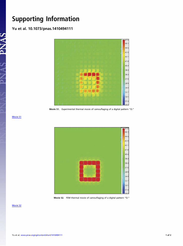
temperature remain confined largely to a single pixel, withoutsignificant diffusion to neighboring pixels (SI Appendix, Fig.S17). The lateral uniformity and pixel-level localization of thechanges in temperature follow from (i) the high thermal con-ductivity of the Ag layer and its ability to facilitate thermal dif-fusion from the diode source (SI Appendix, Fig. S20) and (ii) thepixelated pattern of this material and the leucodye composite.The temperature (see SI Appendix, Fig. S18) is nearly constantthroughout the depth of this composite (see SI Appendix, Fig. S19),due to its thin geometry. These collective features enable arbi-trary pattern generation to a resolution set by the numbers ofpixels and their sizes. An example of a pattern of the character
“O” appears in Movie S1 (experimental results) and Movie S2(modeling results).Experimental procedures used to study camouflage capa-
bilities in cuttlefish (2, 30–33) serve as a model for illustratingfull function, i.e., metachrosis, of the systems. Here, a devicerests on a patterned black-and-white background formed bypassing white light through an amplitude mask from below.External control electronics automatically send signals to theactuators at locations where responses from associated photo-detectors exceed a threshold. Fig. 3A shows a case in which allpixels turn white, consistent with the uniformly bright pattern ofthe background. Different static geometries, including triangles,
00:3.94 00:17.23 00:28.77 00:34.01
A
B
00:8.48 00:15.03 00:22.70 00:32.34
00:48.19 01:21.93 01:30.24 01:34.66
00:49.39 01:07.27 01:22.18 01:38.26
Fig. 4. Two demonstrations of autonomous, dynamic metachrosis. (A) Sequence of images extracted from a movie (time stamp in the lower right) thatdemonstrates adaptive pattern matching to a continuously changing background, created in this case by moving a mask that allows passage of light througha square region. At the top are angled view schematic illustrations of the experiment (top: device; bottom: pattern background). (B) Results similar to those inA, but obtained with a different mask geometry.
13002 | www.pnas.org/cgi/doi/10.1073/pnas.1410494111 Yu et al.

arrays of dots, and even random patterns, can be achieved, witheither flat or curved configurations, as shown in Fig. 3 B−E.Dynamic pattern recognition and matching are also possible,
as illustrated in Fig. 4 A and B. In this case, changing the positionof an amplitude mask that passes light only through a smallsquare region leads to corresponding changes in the displayedpatterns (Fig. 4A). In these images and others of Fig. 4, the topillustrations correspond to schematic, angled view renderings ofthe mask and the device; the images directly below are top viewsof the device. Movies S3 and S4 show additional details andexamples. The metachrosis process occurs within 1 or 2 s in allcases, which is similar to neutrally controlled pattern change incephalopods (2).
DiscussionThese systems establish foundations in materials science andengineering design that address key challenges in distributedsensing, actuation, and control in adaptive camouflage. Thesensors and actuators provide operation across the full visiblespectrum and allow for electric-field– or current-inducedswitching, respectively. As a result, these ideas can be applied notonly with simple thermochromic materials but also with moreadvanced alternatives that offer improved power efficiency,facile routes to color, and robust operation without sensitivity toenvironmental conditions. Furthermore, the overall architecturecan accommodate integration of tunable analogs to iridophores,thereby providing a vehicle for future investigations. In all cases,compatibility with large-area electronics holds promise for scal-able manufacturing. Ability to reproduce physical texture, as inmany cephalopods (34), remains as an interesting and chal-lenging topic for research.
Materials and MethodsFabrication and Assembly. Detailed fabrication procedures for the variousindividual components of the system appear in SI Appendix. The assembly
process involves a series of lamination processes. First, a slab of PDMS(Sylgard 184, Dow Corning) was used to retrieve an interconnected array ofmultiplexed silicon diodes after release from a glass substrate. Exposinga separate layer of PDMS (100 μm, on a glass substrate) to UV-induced ozone(BHK, Inc.) generated a hydroxyl-terminated surface for bonding via con-densation reactions with similar chemistry associated with a layer SiO2
blanket deposited onto the array. The Ag (thickness 300 nm) and the ther-mochromic composite (thickness ∼65 μm) were lithographically patterned ontop of the diode array. Alignment followed a scheme shown in SI Appendix,Fig. S10C. The resulting system, with the PDMS layer, was then peeled fromthe glass. Similar bonding processes enabled aligned integration of a sepa-rately fabricated multiplexed array of photodetectors onto the backside ofthe PDMS, through the use of modified mask aligner (MJB-3, Karl Suss) withalignment accuracy of 1 μm. Details appear in SI Appendix, Fabrication andassembling the complete system and Fig. S9.
Control and System Operation. The system consists of two sets of activecomponents, i.e., sensors and actuators, each of which functions separatelyand at different multiplexed scanning speeds. Closed-loop operation involves(i) acquiring digital images based on the intensity distributions extractedfrom responses of the 16 × 16 array of photodetectors, (ii) binarizing theintensity distribution and storing the resulting data in a buffer, and (iii)reading the buffer and addressing the 16 × 16 array of actuators by columnscanning to copy the pattern, in a repeating manner. The time to acquire animage is ∼10 ms, much shorter than the pulse period for actuation (280 ms),thereby ensuring that the refresh rate of the image exceeds that of inducedcolor change. Software development tools from LabVIEW 2012 provide all ofthe necessary means for implementation of the described operation.
ACKNOWLEDGMENTS. Jeff Grau is acknowledged for his help in preparingphotomasks. The work on material design and device fabrication wassupported by Office of Naval Research under Grant N00014-10-1-0989.C.Y. acknowledges the start-up funding support from the Department ofMechanical Engineering, Cullen College of Engineering, and the Divisionof Research at the University of Houston. R.T.H. also acknowledges par-tial support from Air Force Office of Scientific Research Grant FA9550–09–0346.
1. Mäthger LM, Denton EJ, Marshall NJ, Hanlon RT (2009) Mechanisms and behaviouralfunctions of structural coloration in cephalopods. J R Soc Interface 6(Suppl 2):S149–S163.
2. Hanlon R (2007) Cephalopod dynamic camouflage. Curr Biol 17(11):R400–R404.3. Hanlon RT, et al. (2009) Cephalopod dynamic camouflage: Bridging the continuum
between background matching and disruptive coloration. Philos Trans R Soc Lond BBiol Sci 364(1516):429–437.
4. Messenger JB (2001) Cephalopod chromatophores: Neurobiology and natural history.Biol Rev Camb Philos Soc 76(4):473–528.
5. Hanlon RT (1982) The functional-organization of chromatophores and iridescent cellsin the body patterning of Loligo-plei (Cephalopoda, Myopsida). Malacologia 23(1):89–119.
6. Manakasettharn S, Taylor JA, Krupenkin TN (2011) Bio-inspired artificial iridophoresbased on capillary origami: Fabrication and device characterization. Appl Phys Lett99(14):144102.
7. Morin SA, et al. (2012) Camouflage and display for soft machines. Science 337(6096):828–832.
8. Rossiter J, Yap B, Conn A (2012) Biomimetic chromatophores for camouflage and softactive surfaces. Bioinspir Biomim 7(3):036009.
9. Phan L, et al. (2013) Reconfigurable infrared camouflage coatings from a cephalopodprotein. Adv Mater 25(39):5621–5625.
10. Coles HJ, Pivnenko MN (2005) Liquid crystal ‘blue phases’ with a wide temperaturerange. Nature 436(7053):997–1000.
11. Kahn FJ (1970) Electric-field-induced color changes and pitch dilation in cholestericliquid crystals. Phys Rev Lett 24(5):209–212.
12. Kikuchi H, Yokota M, Hisakado Y, Yang H, Kajiyama T (2002) Polymer-stabilized liquidcrystal blue phases. Nat Mater 1(1):64–68.
13. Sackmann E (1971) Photochemically induced reversible color changes in cholestericliquid crystals. J Am Chem Soc 93(25):7088–7090.
14. Comiskey B, Albert JD, Yoshizawa H, Jacobson J (1998) An electrophoretic ink for all-printed reflective electronic displays. Nature 394(6690):253–255.
15. Heikenfeld J, et al. (2009) Electrofluidic displays using Young−Laplace transpositionof brilliant pigment dispersions. Nat Photonics 3(5):292–296.
16. Vukusic P, Sambles JR (2003) Photonic structures in biology. Nature 424(6950):852–855.
17. Arsenault AC, et al. (2006) From colour fingerprinting to the control of photo-luminescence in elastic photonic crystals. Nat Mater 5(3):179–184.
18. Harun-Ur-Rashid M, Seki T, Takeoka Y (2009) Structural colored gels for tunable soft
photonic crystals. Chem Rec 9(2):87–105.19. Kim H, et al. (2009) Structural colour printing using a magnetically tunable and
lithographically fixable photonic crystal. Nat Photonics 3(9):534–540.20. Wang C, et al. (2013) User-interactive electronic skin for instantaneous pressure vi-
sualization. Nat Mater 12(10):899–904.21. Boer W, Abileah A (2005) US Patent 6,947,102 B2.22. Choi J, Joo I, Kim H (2010) US Patent 7,800,602 B2.23. Kreit E, et al. (2012) Biological versus electronic adaptive coloration: How can one
inform the other? J R Soc Interface 10(78):20120601.24. Mäthger LM, Hanlon RT (2007) Malleable skin coloration in cephalopods: Selective
reflectance, transmission and absorbance of light by chromatophores and irido-
phores. Cell Tissue Res 329(1):179–186.25. Mathger LM, et al. (2013) Bright white scattering from protein spheres in color
changing, flexible cuttlefish skin. Adv Funct Mater 23(32):3980–3989.26. Mäthger LM, Roberts SB, Hanlon RT (2010) Evidence for distributed light sensing in
the skin of cuttlefish, Sepia officinalis. Biol Lett 6(5):600–603.27. Anonymous (2002) Chemistry and Applications of Leuco Dyes (Plenum, New York).28. Siegel AC, Phillips ST, Wiley BJ, Whitesides GM (2009) Thin, lightweight, foldable
thermochromic displays on paper. Lab Chip 9(19):2775–2781.29. Yu C, et al. (2014) All-elastomeric, strain-responsive thermochromic color indicators.
Small 10(7):1266–1271.30. Forsythe JW, Hanlon RT (1988) Behavior, body patterning and reproductive biology of
Octopus bimaculoides from California. Malacologia 29(1):41–55.31. Hanlon RT, Messenger JB (1988) Adaptive coloration in young cuttlefish (Sepia offi-
cinalis l) - the morphology and development of body patterns and their relation to
behavior. Philos Trans R Soc Lond B Biol Sci 320(1200):437–487.32. Mäthger LM, et al. (2007) Disruptive coloration elicited on controlled natural sub-
strates in cuttlefish, Sepia officinalis. J Exp Biol 210(Pt 15):2657–2666.33. Zylinski S, Osorio D, Shohet AJ (2009) Cuttlefish camouflage: Context-dependent
body pattern use during motion. Proc R Soc B 276(1675):3963–3969.34. Allen JJ, Bell GRR, Kuzirian AM, Velankar SS, Hanlon RT (2014) Comparative mor-
phology of changeable skin papillae in octopus and cuttlefish. J Morphol 275(4):
371–390.
Yu et al. PNAS | September 9, 2014 | vol. 111 | no. 36 | 13003
ENGINEE
RING

1
Supporting Information
Adaptive optoelectronic camouflage systems with designs inspired by cephalopod skins
Cunjiang Yua, Yuhang Li
b,c, Xun Zhang
d, Xian Huang
d, Viktor Malyarchuk
d, Shuodao Wang
d,
Yan Shib,e
, Li Gaod, Yewang Su
b, Yihui Zhang
b, Hangxun Xu
f, Roger Hanlon
g,h, Yonggang
Huangb, and John A. Rogers
d,i,1
aDepartment of Mechanical Engineering, Department of Electrical and Computer Engineering,
University of Houston, Houston, TX 77204
bDepartment of Civil and Environmental Engineering, Department of Mechanical Engineering,
Center for Engineering and Health, and Skin Disease Research Center, Northwestern University,
Evanston, IL 60208
cThe Solid Mechanics Research Center, Beihang University, Beijing 100191, China
dDepartment of Materials Science and Engineering, University of Illinois at Urbana-Champaign,
Urbana, IL 61801
eState Key Laboratory of Mechanics and Control of Mechanical Structures, Nanjing University
of Aeronautics and Astronautics, Nanjing 210016, China
fDepartment of Polymer Science and Engineering, CAS Key Laboratory of Soft Matter Chemistry,
University of Science and Technology of China, Hefei 230026, China
gMarine Biological Laboratory, Woods Hole, MA, 02543
hDepartment of Ecology and Evolutionary Biology, Brown University, Providence, RI, 02912
iDepartment of Electrical and Computer Engineering, Department of Chemistry, Department of
Mechanical Science and Engineering, Frederick-Seitz Materials Research Laboratory, and
Beckman Institute for Advanced Science and Technology, University of Illinois at Urbana-
Champaign, Urbana, IL 61801


3
1. Preparing the thermochromic composite and measuring its optical characteristics
Preparation of the photodefinable thermochromic composite involved mixing
microencapsulated leuco dye (black 47C, LCR Hallcrest) with SU-8 50 (Microchem, USA) at a
weight ratio of 1:5 to form a liquid slurry. Microcapsules contain mixtures of leuco dye with a
color developer and a low melting point solvent. At low temperatures, the developer and leuco
dye form a complex that favors a colored ring-open state. Upon heating, the solvent melts, and
the developer and dye dissociate. In this state, the leuco dye favors a colorless, ring-closed
configuration. Such transformation occurs at 47 °C in a reversible manner. Figure S1A shows an
optical image of the slurry at 22 °C. Heating to a temperature above 47 °C causes the slurry to
become transparent. As shown in Fig. S1B, a background picture underneath the slurry is clearly
visible at temperatures above 47 °C. Standard procedures for pattering SU-8 yield pixelated
arrays of this slurry with thickness defined by the spin-speed. Figures S1C and D provide SEM
images of examples. Detailed fabrication steps appear below.
The optical reflectance of the color changeable pixels (Ag/composite dye) was measured using
a spectrometer (Cary 5G UV-VIS-NIR) as a function of temperature. A portable thermoelectric
heater/cooler (InbS1-031.021, WATRONIX, Inc.) served to control the sample temperature. A
thermocouple (Fluke 233, Fluke Corporation) was used to measure the temperature.
Fabrication steps:
1. Mix leuco dye and SU-8 50 at weight ratio of 1:5.
2. Spin-coat the mixture slurry (3000rpm, 30 sec).
3. Pre-bake at 65 °C for 5 min and 95 °C for 20 min.
4. Expose to UV light under a mask aligner (Karl Suss MJB3) at a dose of 1440 mJ/cm2.
5. Post-bake at 65 °C for 2 min and 95 °C for 5 min.

4
6. Develop in SU-8 developer (MicroChem, USA) for 6 minutes.
7. Rinse in isopropyl alcohol (IPA) and deionized (DI) water.
2. Fabricating the diode array and measuring its electrical characteristics
Figure S2A shows an exploded schematic illustration of the layout of the Si, metal and
polyimide (PI) layers associated with a single pixel in the heater array. The major steps in the
fabrication include retrieving a thin (1.25 m) crystalline film of Si with pre-defined patterns of
doping from a silicon-on-insulator (SOI) wafer followed by transfer printing onto a thin
polyimide (PI) substrate, and then applying layers for metallization and passivation, as outlined
in Figs. S3 and 4. A thin layer of gold eliminates the potential for crosstalk induced by light.
Figure S2B shows the planar structure and design of the Si heater; the small dots correspond to
holes introduced into the Si to facilitate chemical etching for release. The measured I-V curves at
different temperatures appear in Fig. 2B. Figure S2C shows an optical image of a 16×16 array of
unit cells. Individual addressing is achieved without affecting the neighborhood pixels, as
evidenced by the IR image (QFI InfraScope II) of Fig. S2D. Here, the background temperature
was set to 30 °C, to facilitate IR imaging. Detailed fabrication steps are as follows.
Fabrication steps:
Defining alignment markers
1. Clean 1.25 μm SOI wafer (acetone, isopropyl alcohol (IPA), deionized (DI) water).
2. Pattern photoresist (PR; Clariant AZ5214, 3000 rpm, 30 sec) with 365 nm optical lithography
(Mask #1: Alignment marker).
3. Etch Si by RIE (50 mTorr, 40 sccm SF6, 100 Watt, 1 min).
4. Remove PR by acetone and clean by piranha for 10 min.
Performing p+ doping

5
5. Deposit 900 nm SiO2 by plasma enhanced chemical vapor deposition (PECVD;
PlasmaTherm SLR).
6. Treat with hexamethyldisilazane (HMDS) for 2 min.
7. Pattern PR (Mask #2: P doping).
8. Bake at 110°C for 5 min.
9. Etch SiO2 in buffered oxide etchant (BOE, 6:1) for 1.5 min.
10. Remove PR by acetone and clean by piranha for 10 min.
11. Expose to a boron doping source at 1000°C for 30 min.
12. Clean the processed wafer (concentrated (49%) HF 2 min, piranha 10 min, BOE 1 min).
Performing n+ doping
13. Deposit 900 nm SiO2 by PECVD.
14. Treat with HMDS for 2 min.
15. Pattern PR (Mask #3: N doping).
16. Bake at 110°C for 5 min.
17. Etch SiO2 in buffered oxide etchant (BOE, 6:1) for 1.5 min.
18. Remove PR by acetone and clean by piranha for 10 min.
19. Expose to a phosphorus doping source at 1000°C for 10 min.
20. Clean the processed wafer (HF 2 min, piranha 10 min, BOE 1 min).
Releasing the top Si from SOI
21. Pattern PR (AZ 5214) (Mask #4: Releasing hole 1).
22. Etch Si by RIE (50 mTorr, 40 sccm SF6, 100 Watt, 3.5 min).
23. Remove PR by acetone and clean by piranha for 10 min.
24. Etch buried oxide layer in concentrated HF for 45 min.

6
25. Rinse and clean the processed wafer in DI wafer.
Retrieving the Si film
26. Bring a 6 mm thick PDMS (weight ratio of base: curing agent=10:1) stamp into contact with
the Si.
27. Peel the stamp back to lift the Si film from SOI onto the stamp.
Preparing the carrier wafer
28. Spin cast polyimide (PI, poly(pyromellitic dianhydride-co-4,4’-oxydianiline) (4000 rpm, 30
sec) onto a 3”×2” glass slide.
29. Anneal at 150 °C for 10 min.
30. Anneal at 250 °C for 60 min in an N2 atmosphere.
31. Deposit Cr/Au (5/300 nm) by electron beam evaporation (AJA International).
Transfer printing the Si film
32. Spin coat the carrier wafer with PI (4000 rpm, 30 sec).
33. Bake at 110 °C for 30 sec.
34. Bring the stamp with Si film on its surface into contact with the carrier wafer.
35. Bake at 110 °C for 30 sec.
36. Remove the PDMS stamp, leaving the Si on carrier wafer
37. Anneal at 150 °C for 10 min.
38. Anneal at 250 °C for 60 min in N2 atmosphere.
Isolating the PIN heaters
39. Pattern PR (Mask #5: Diode isolation).
40. Etch Si by RIE (50 mTorr, 40 sccm SF6, 100 Watt, 3.5 min).
41. Remove PR by acetone.

7
Patterning metal to block light
42. Pattern PR (AZ 4620, 3000 rpm, 30 sec) (Mask #6: Back light blocking metal).
43. Etch PI by RIE (MARCH, 300 mTorr, 150 Watt, 10 min).
44. Wet etch exposed Au/Cr for 54/7 sec.
45. Remove PR by acetone.
Defining the via hole to the p contact
46. Spin coat PI (4000 rpm, 30 sec).
47. Anneal at 150°C for 10 min.
48. Anneal at 250°C for 60 min in N2 atmosphere.
49. Pattern PR (AZ 4620) (Mask #7: P via hole).
50. Etch PI by RIE (MARCH, 300 mTorr, 150 Watt, 10 min).
51. Remove PR by acetone.
Defining the metal for the p contact
52. Deposit Cr/Au (5/300 nm) by DC sputtering (AJA International).
53. Pattern PR (AZ 5214) (Mask #8: P metal).
54. Wet etch exposed Au/Cr for 54/7 sec.
55. Remove PR by acetone.
Defining the via hole to the n contact
56. Spin coat PI (4000 rpm, 30 sec).
57. Anneal at 150°C for 10 min.
58. Anneal at 250°C for 60 min in N2 atmosphere.
59. Pattern PR (AZ 4620) (Mask #9: N via hole).
60. Etch PI by RIE (MARCH, 300 mTorr, 150 Watt, 20 min).

8
61. Remove PR by acetone.
Defining the metal for the n contact
62. Deposit Cr/Au (5/300 nm) by DC sputtering (AJA International).
63. Pattern PR (AZ 5214) (Mask #10: N metal).
64. Wet etch exposed Au/Cr for 54/7 sec.
65. Remove PR by acetone.
Depositing PI encapsulation
66. Spin coat PI (4000 rpm, 30 sec).
67. Anneal at 150°C for 10 min.
68. Anneal at 250°C for 60 min in N2 atmosphere.
Releasing the device
69. Deposit 150 nm SiO2 by PECVD.
70. Treat with HMDS for 2 min.
71. Pattern PR (Mask #11: Releasing hole 2).
72. Etch SiO2 by RIE (50 mTorr, 40:1.2 sccm CF4:O2, 150 Watt, 8.5 min).
73. Remove PR by acetone.
74. Release device in BOE (6:1).
3. Fabricating the photodetector array and measuring its characteristics
Figure S7A shows an exploded schematic illustration of the layout of the Si, metal and PI
layers associated with a single unit cell in the photodetector array. The major steps in the
fabrication are similar to those for the heater array. Every unit cell in the photodetector array
includes a photodiode and blocking diode constructed in a back-to-back configuration to
eliminate crosstalk in passive matrix readout. In addition, the light sensitive intrinsic region of

9
the blocking diode is covered by a layer of Cr/Au to eliminate any response to light. Figure S7B
shows the planar structure design of the photodetector. An optical image of the thin
photodetector array appears in Fig. S7C. Detailed fabrication steps are as follows.
Fabrication steps:
Defining alignment markers
1. Clean 1.25 μm SOI wafer with acetone, IPA and DI water.
2. Pattern PR (AZ5214) (Mask #1: Alignment marker).
3. Etch Si by RIE (50 mTorr, 40 sccm SF6, 100 Watt, 1 min).
4. Remove PR by acetone and clean by piranha for 10 min.
Performing p+ doping
5. Deposit 900 nm SiO2 by PECVD.
6. Treat with HMDS for 2 min.
7. Pattern PR (Mask #2: P doping).
8. Bake at 110°C for 5 min.
9. Etch SiO2 in BOE (6:1) for 1.5 min.
10. Remove PR by acetone and clean by piranha for 10 min.
11. Expose to a boron doping source at 1000°C for 30 min.
12. Clean the processed wafer (HF 2 min, piranha 10 min, BOE 1 min).
Performing n+ doping
13. Deposit 900 nm SiO2 by PECVD,
14. Treat with HMDS for 2 min.
15. Pattern PR (Mask #3: N doping).
16. Bake at 110°C for 5 min.

10
17. Etch SiO2 in buffered oxide etchant (BOE, 6:1) for 1.5 min.
18. Remove PR by acetone and clean by piranha for 10 min.
19. Expose to a phosphorus doping source at 1000°C for 10 min.
20. Clean the processed wafer (HF 2 min, piranha 10 min, BOE 1 min).
Releasing top Si from SOI
21. Pattern PR (AZ 5214) (Mask #4: Releasing hole 1).
22. Etch Si by RIE (50 mTorr, 40 sccm SF6, 100 Watt, 3.5 min).
23. Remove PR by acetone and clean by piranha for 10 min.
24. Etch buried oxide layer in concentrated HF for 45 min.
25. Rinse and clean the processed wafer in DI wafer.
Retrieving the Si film
26. Bring a 6 mm thick PDMS (weight ratio of base: curing agent=10:1) stamp into contact with
the Si.
27. Peel the stamp back to lift the Si film from SOI onto the stamp.
Preparing the carrier wafer
28. Spin cast PI (4000 rpm, 30 sec) onto a 3”×2” glass slide
29. Anneal at 150°C for 10 min.
30. Anneal at 250°C for 60 min in N2 atmosphere.
31. Deposit Cr/Au (5/300 nm) by electron beam evaporation.
Transfer printing the Si film
32. Spin coat the carrier wafer with PI (4000 rpm, 30 sec).
33. Bake at 110°C for 30 sec.
34. Bring the stamp with Si film on onto contact with the carrier wafer.

11
35. Bake 110°C for 30 sec.
36. Retrieve the PDMS stamp, leaving the Si on carrier wafer.
37. Anneal at 150°C for 10 min.
38. Anneal at 250°C for 60 min in N2 atmosphere.
Isolating the photodetectors
39. Pattern PR (Mask #5: Photodetector isolation).
40. Etch Si by RIE (50 mTorr, 40 sccm SF6, 100 Watt, 3.5 min).
41. Remove PR by acetone.
Patterning metal to block light
42. Pattern PR (AZ 4620, 3000 rpm, 30 sec) (Mask #6: Back light blocking metal).
43. Etch PI by RIE (MARCH, 300 mTorr, 150 Watt, 10 min).
44. Wet etch exposed Au/Cr for 54/7 sec.
45. Remove PR by acetone.
Defining via 1
46. Spin coat PI (4000 rpm, 30 sec).
47. Anneal at 150°C for 10 min.
48. Anneal at 250°C for 60 min in a N2 atmosphere.
49. Pattern PR (AZ 4620) (Mask #7: Via hole 1).
50. Etch PI by RIE (MARCH, 300 mTorr, 150 Watt, 10 min).
51. Remove PR by acetone.
Depositing and patterning metal 1
52. Deposit Cr/Au (5/300 nm) by DC sputtering (AJA International).
53. Pattern PR (AZ 5214) (Mask #8: Metal 1).

12
54. Wet etch exposed Au/Cr for 54/7 sec.
55. Remove PR by acetone.
Patterning via 2
56. Spin coat PI (4000 rpm, 30 sec).
57. Bake at 150 °C for 10 min.
58. Anneal at 250 °C for 60 min in N2 atmosphere.
59. Pattern PR (AZ 4620) (Mask #9: Via hole 2).
60. Etch PI by RIE (MARCH, 300 mTorr, 150 Watt, 20 min).
61. Remove PR by acetone.
Depositing and patterning metal 2
62. Deposit Cr/Au (5/300 nm) by DC sputtering (AJA International).
63. Pattern PR (AZ 5214) (Mask #10: Metal 2).
64. Wet etch exposed Au/Cr for 54/7 sec.
65. Remove PR by acetone.
Depositing PI encapsulation
66. Spin coat PI (4000 rpm, 30 sec).
67. Anneal at 150 °C for 10 min.
68. Anneal at 250 °C for 60 min in N2 atmosphere.
Opening the bonding pad
69. Cover the device with a 2 mm thick piece of PDMS and expose the bonding pad.
70. Etch the unprotected PI (MARCH, 300 mTorr, 150 Watt, 10 min) to expose the bonding pad.
Releasing the device
71. Deposit 150 nm SiO2 by PECVD.

13
72. Treat with HMDS for 2 min.
73. Pattern PR (Mask #11: Releasing hole 2).
74. Etch SiO2 by RIE (50 mTorr, 40:1.2 sccm CF4:O2, 150W, 8.5 min).
75. Remove PR by acetone.
76. Release device in BOE (6:1).
4. Fabricating and assembling the complete system
Assembling the complete system involves multiple steps of functional component fabrication
and integration. Detailed fabrication steps are outlined in the following.
Fabrication steps:
Bonding the heater array with thin PDMS
1. Retrieve the thin heater array with a PDMS stamp.
2. Deposit 40 nm SiO2 by PECVD.
3. Spin coat PDMS (10:1, 500rpm, 1 min) on a glass slide (2”×3”).
4. Bake at 80°C for 10 min.
5. Treat the front surface of the PDMS under a UVO lamp (BHK Inc.) for 5 min.
6. Bond the heater array with the treated PDMS.
Constructing the artificial leucophor and chromatophore pixels
7. Deposit Ag (300 nm) for the white background and heat spreading layer by electron beam
evaporation.
8. Pattern PR (AZ 5214) (Mask #1: Ag).
9. Etch exposed Ag by wet etchants for 20 sec.
10. Remove PR by acetone.

14
11. Pattern the thermochromic composite by spin coating, pre-baking, exposing, post-baking and
developing.
12. Clean with isopropyl alcohol (IPA) and deionized (DI) water.
Opening the bonding pad for the heater
13. Cover the device by a rectangular, ring-shaped piece of PDMS (2 mm thick) with a glass
slide on top and expose the bonding pad.
14. Etch the unprotected PI (MARCH, 300 mTorr, 150 Watt, 10 min) to expose the bonding pad.
15. Peel off the PDMS with the heater and color changeable pixel array from the glass slide.
Bonding the photodetector array
16. Treat the back surface of the PDMS under a UVO lamp for 5 min.
17. Retrieve the photodetector array with a PDMS stamp.
18. Deposit 40 nm SiO2 by PECVD.
19. Align and bond the photodetector array to the activated rear surface of the PDMS with all
other components on the front side.
5. Optical system and data acquisition
Connecting the pins on a custom printed circuit board (PCB) that is interfaced to the devices,
with control electronics and software enables background image acquisition, signal processing,
and pulse power signal generation. Electronic diagrams for image acquisition are shown in Fig.
S7D. The inputs and outputs, i.e. the columns and rows respectively, are interfaced with the
control electronics of NI PXIe-6363(National Instruments). The current responses at an applied
bias of 3 V were measured for all the pixels in the 16 x 16 array, used to generate the image
results of Fig. S8. Three different light intensities ranging from bright, working to complete
darkness served to test the detector arrays. A good range of sensitivity is possible for the

15
photodetecting pixels, from current responses of 1100~1200 nA at the highest brightness to
0.5~3 nA in the dark state, as shown in Fig. 2C. The greyscale image of Fig. S8A represents the
normalized photocurrent intensity map during image acquisition, while the binarized image by
choosing the cut-off value of 0.25 was achieved as shown in Fig. S8B. The binarized data were
used to control the pulse voltages to supply the heaters, thus to induce color change and pattern
matching.
The circuit diagram of the heater array is shown in Fig. S5. Instead of directly interfacing the
devices with the PXI control electronics, the heaters were powered using the output of a
transistor (MCT2EM-ND, Fairchild Semiconductor Corp.) capable of meeting the power
requirements. Figure S6 shows the controlling pulse (3 V) from the PXIe-6723 and the power
supply pulse (12 V). The voltage directly applied to the heater pixel is 10.5 V, since there is
some voltage drop on the two forward biased junctions from the circuit.
6. Moving background setup and device testing
The changeable background, which was used to verify the camouflaging capabilities,
consisted of a backlight and a transparency mask. Specifically, diffusive light from an array of
light emitting diodes (MB-BL4X4, Metaphase Technologies, Inc., USA) provided a uniform,
white light illumination. The plastic transparency masks consist of various black patterns that
block the light. Motion of this mask relative to the device system allowed demonstrations of
dynamic change of the patterns. The schematic cartoons with various patterns are shown in Fig.
4. The whole setup was built on a stage to allow temperature control, with a set point of .

16
7. Thermal analysis
FEM, specifically the continuum element DC3D8 in the ABAQUS software(1), was used to
study the temperature distribution in the device. The substrate, made of PI (thickness 9.95 m)
and PDMS (thickness 100 m), was supported by a glass slide (thickness 1100 m). As shown
in Fig. S16A, the device consists of 16 × 16 pixels on the substrate, where each pixel consists of
a layer of composite dye (thickness 65 m) and Ag (thickness 0.3 m) (Fig. S16B). The pixels
have spacing of 100 m, and in-plane dimensions of 820 × 820 m2 with four corners (each 110
× 110 m2) removed (Fig. S16C). For each pixel, the PI layer underneath contains the (Si)
heater and the gold layer with dimensions of 640 × 640 × 1.25 m3 and 720 × 720 × 0.3 m
3,
respectively (Fig. S2B). Figures S16 A and C also show Au interconnects between the heaters.
The bottom of the glass slide has a constant temperature 40.5 °C, as in experiments. The entire
top surface, and the lateral surfaces of pixels, have natural convection with the coefficient of heat
convection of 5 W/(m2·K) and air temperature of 20 °C. Figure S16D illustrates the pulsed
voltage of U0 = 10.5 V and duration of t0 = 17.5 ms in the period of T = 280 ms.
The thermal conductivity, heat capacity, and mass density are 0.2 W/(m·K), 1800 J/(kg·K),
and 1200 kg/m3 for thermochromic dye(2, 3); 371 W/(m·K), 235 J/(kg·K), and 10492 kg/m
3 for
silver(4); 0.52 W/(m·K), 1090 J/(kg·K), and 1420 kg/m3 for PI(5, 6); 160 W/(m·K), 700 J/(kg·K),
and 2329 kg/m3 for silicon(7); 317 W/(m·K), 129 J/(kg·K), and 19280 kg/m
3 for gold(8, 9); 0.18
W/(m·K), 970 J/(kg·K), and 1460 kg/m3 for PDMS(7); 1.2 W/(m·K), 790 J/(kg·K), and 2700
kg/m3 for glass(10), respectively.
Figure S17A shows the temperature distribution, obtained by FEM, along the plane of the Si
heaters (x direction) as illustrated in Fig. S17B, when all heaters are off except the center one,
which receives pulsed power, and the temperature fluctuation is stabilized. The maximum

17
temperature increase in all heaters without power is only 3% of that in the center heater, which
clearly demonstrates that the heat is well confined. Figure S18 shows that, during thermal
fluctuation due to pulsed power, the maximum temperature on the surface of the heated pixel
ranges from 57 to 65 °C. The temperature along z direction (normal to the surface) given in Fig.
S19 suggests relatively uniform temperature across the thickness of the dye. Figure S20
compares the temperature distributions at the bottom surface of the dye, with and without the Ag
layer. With Ag, the temperature is more uniform than that of the case of without Ag layer.
8. Mechanical analysis
This analysis of strains and stresses in the device during bending by FEM upon application of
a load along the x and y directions is performed. The thermochromic composite dye and PDMS
are modeled as three-dimensional solids. The multilayer structures consist of metal, silicon and
PI, are modeled as shells. The Young’s modulus and Poisson’s ratio are 130 GPa and 0.27 for
silicon, 78 GPa and 0.44 for Au, 2 MPa and 0.49 for PDMS and 2.5 GPa and 0.34 for PI,
respectively. Figure S12B captures the maximum strain in the silicon for bending to different
bending radii.

18
References
1. ABAQUS Analysis User’s Manual V6.9 (2009) (Dassault Systémes, Pawtucket).
2. Kim TI, et al. (2012) High-efficiency, microscale GaN light-emitting diodes and their
thermal properties on unusual substrates. Small 8(11):1643-1649.
3. Solano B, Rolt S, & Wood D (2008) Thermal and mechanical analysis of an SU8
polymeric actuator using infrared thermography. Proc Inst Mech Eng C J Mech Eng Sci
222(1):73-86.
4. Smith DR & Fickett FR (1995) Low-temperature properties of silver. J Rre Natl Inst Stan
100(2):119-171.
5. Dhorajiya AP, et al. (2010) Finite element thermal/mechanical analysis of transmission
laser microjoining of titanium and polyimide. ASME J Eng Mater Technol 132(1)
011004.
6. Hu ZL, Carlberg B, Yue C, Guo XM, & Liu JH (2009) Modeling of nanostructured
polymer-metal composite for thermal interface material applications. in 2009
International Conference on Electronic Packaging Technology & High Density
Packaging, pp 405-408.
7. Li R, et al. (2012) Thermo-mechanical modeling of laser-driven non-contact transfer
printing: two-dimensional analysis. Soft Matter 8(27):7122-7127.
8. Bourgoin JP, Allogho GG, & Hache A (2010) Thermal conduction in thin films measured
by optical surface thermal lensing. J Appl Phys 108(7):073520.
9. J. F. Shackelford WA (2001) CRC Materials Science and Engineering Handbook (CRC
Press LLC).

19
10. Tari M, et al. (2003) A high voltage insulating system with increased thermal
conductivity for turbo generators. Proceedings: Electrical Insulation Conference and
Electrical Manufacturing & Coil Winding Technology Conference, pp 613-617.

20
Supplementary Movie Legends
Movie S1. Experimental thermal movie of camouflaging of a digital pattern “O”.
Movie S2. FEM thermal movie of camouflaging of a digital pattern “O”.
Movie S3. Movie of dynamic, adaptive pattern recognition and color camouflaging against a
moving square background. The video is sped up by 3 times.
Movie S4. Movie of dynamic, adaptive pattern recognition and color camouflaging on a
changing background. The video is sped up by 3 times.
Supplementary Figure Legends
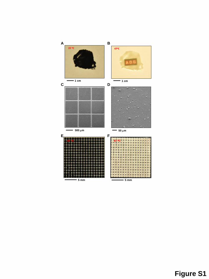
Figure S1. (A) Optical image of the black thermochromic slurry at room temperature, ~22°C. (B)
Optical image of the slurry at 47°C. At this temperature, the slurry is transparent, thereby a
background picture underneath is visible. (C) SEM image of an array of photopatterned
thermochromic pixels. (D) SEM image of the top surface of a patterned pixel. (E) Optical image
of the pixel arrays (16×16) at room temperature of 22°C. (F) Optical image of the arrays (16×16)
at 47°C.
Figure S2. (A) Exploded schematic illustration of the layout of the Si, metal, and PI layers of a
single pixel in the heater array. (B) Optical image of the Si diode. The dark dots represent the
releasing holes etched through the Si. (C) Optical image of the heater array. (D) Thermal image
of the array with one pixel activated. The heat is mostly confined within the area of the activated
heater, with minimal changes in neighboring pixels. The background temperature was set to
30°C.

21
Figure S3. Schematic illustration of the major steps for fabricating flexible devices based on Si
nanomembranes. (A) Preparing the device elements by selective doping. (B) Opening holes and
undercut etching in concentrated HF. (C) Retrieving the Si from the SOI wafer using a PDMS
stamp. (D) Printing the Si onto a glass substrate with a thin layer of PI. (E) Peeling away the
stamp to leave the Si on the glass. (F) Patterning the Si and completing the metallization and
passivation steps. (G) Releasing the flexible device from the glass.
Figure S4. (A) Optical images of a diode heater with P+ and N
+ doping regions on an SOI wafer.
(B) Optical image of a 1.25 m thick Si membrane on a PDMS stamp. (C) Optical image of the
Si membrane transfer printed onto a glass substrate which was coated with PI. (D) Optical image
of a flexible array of diode heater held by a tweezer.
Figure S5. Schematic circuit diagram of a heater array and its external circuits.
Figure S6. Images of representative pulse signals. (A) The green curve is the control signal
generated with a program created in Labview. The yellow curve is the output pulse applied to the
heater. (B) Magnified image of both curves.
Figure S7. (A) Exploded schematic illustration of the layout of the Si, metal, and PI layers of a
single pixel in the photodetector array. (B) Schematic illustration of the photodiode and blocking
diode. (C) Optical image of the thin flexible photodetector array folded on a glass slide. (D)
Schematic circuit diagram of the photodetector array.

22
Figure S8. (A) Normalized photocurrent intensity map associated with a digital pattern in the
geometry of the text “UIUC MRL”. (B) Corresponding binarized intensity map.
Figure S9. Schematic steps for assembling the entire system. (A) Schematic illustration of a unit
cell of the heater array and a thin PDMS substrate, prior to bonding. (B) Illustration of the
bonded device. (C) Illustration of the Ag pixel fabricated on the device. (D) Illustration of a unit
cell of the thermochromic pixel on top of the Ag pixel and the photodetector to be bonded
together. (E) Illustration of the integrated system.
Figure S10. (A) Optical image of the heater array on a PDMS substrate. (B) Optical image of the
Ag pixels fabricated on the heater array. (C) Optical image of the heater array and Ag pixels
viewed from the backside.
Figure S11. Optical image of the device with ACF cable and custom made PCB with pin
connectors.
Figure S12. (A) FEM model of the system, showing a 5×5 array. (B) FEM results of the
maximum strain in the Si within the device at different bending radii. The red dots are the results
for bending along x axis. The blue dots are the results for bending along y axis.
Figure S13. (A-H) IR images of the device when one pixel is actuated, as the actuation voltage
increases from 5.5 V to 12.5 V, with an increment of 1 V.

23
Figure S14. (A-D) IR images of the device when 8 pixels (digital pattern of “o”) are actuated, as
the actuation voltage increases from 8.5V to 11.5V, with the increment of 1V.
Figure S15. (A) IR image of the heater array with one pixel activated at 10.5V. The arrow points
to the geometrical center of the pixel. (B) Temperature fluctuation at the center of the pixel. The
power was turned on and off at 11 s and 41 s, respectively. (C) Temperature information during
the period of 20~30 s, as highlighted by the red dotted rectangular in (B).
Figure S16. (A) FEM model for the thermal analysis. (B) Cross-sectional (front) view of the
pixel with the key dimensions. (C) Top view of the pixels. (D) Schematic pulse input for the
FEM simulation.
Figure S17. (A) FEM results of the temperature within the layer of the Si heater arrays. The red
curve shows the maximum temperature, and the black curve represents the minimum
temperature. The results clearly show good heat confinement within the region of the activated
pixel. (B) Schematic cross-sectional view of the heater layer.
Figure S18. (A) FEM results of the temperature along the x axis of the pixel. The black curve
shows the maximum temperature, and the red curve represents the minimum temperature. (B)
Schematic cross-section view of the heater.
Figure S19. (A) FEM results of the temperature across the thickness of the device. The black
curve shows the maximum temperature, and the red curve represents the minimum temperature.

24
(B) Schematic cross-sectional view of the heater pixel.
Figure S20. (A) FEM results of the temperature along the x axis of the pixel for the cases with
and without Ag heat spreading layer. The black curve shows the maximum temperature with the
Ag, and the red curve shows the maximum temperature without Ag. The temperature is more
uniform across the whole pixel with Ag. (B) Schematic cross-sectional view of the heater pixel.
A B
Figure S1
500 mm 50 mm
22 oC
1 cm
47oC
1 cm
C D
5 mm
22 oC 47 oC
5 mm
E F

5 mm
B C
100 mm
D
Figure S2
30
46
80
67
T (oC)
500 mm
A
PI encapsulation
PI support
PI support
PI support
PI support
Back light
blocking metal
P metal
P+ doped
N+ doped
N metal

Figure S3
Open releasing holes, undercut
etching.
Isolation, metallization and passivation.
Si
SiO2
Si
Selective doping on SOI wafers.
SiO2 boundary
Releasing hole
Receiver
Stamp
Releasing device from substrate.
A B
G
d E
Transfer printing to a receiver
substrate for processing.
Apply rubber stamp; peel back
stamp to grab objects.
Apply “inked” stamp to receiving
substrates.
C
D F

Figure S4
A B
1 cm
C D
1 cm
1 cm 1 cm

Heater pixels
Column scan; pulse input
Row control
0
Vcc
Transistor
Figure S5

A
B
Figure S6
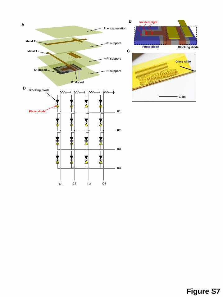
Figure S7
Glass slide
1 cm
Photo diode Blocking diode
Incident light B
C
R1
R2
R3
R4
C1 C2 C3 C4
Photo diode
Blocking diode D
A PI encapsulation
PI support
PI support
PI support
P+ doped
N+ doped
Metal 2
Metal 1

Normalized intensity
A
0.0 0.1
0.2
0.3
0.4
0.5
0.6
0.7
0.8
0.9
1.0
Binarized intensity
0 if ≤ 0.25; 1 if > 0.25.
B
0.0 0.1
0.2
0.3
0.4
0.5
0.6
0.7
0.8
0.9
1.0
Figure S8

Figure S9
PDMS
Heater
Ag
Thermochromic dye
Photodetector
A
B C
D
E

1 mm
A B
1 mm
C
20 mm
Figure S10

Pins to connect to external cable out for
environmental visioning
1 cm
Heater power input connection
Figure S11

Figure S12
Maxim
um
Str
ain
in
Sil
ico
n
(%)
Bending radius (mm)
Bending along x axis
Bending along y axis
2 4 6 8 10
0.2
0.4
0.6
0.8
0
x
y z
A
B

8.5 V 7.5 V 6.5 V
9.5 V
5.5 V
A B C D
E F G 10.5 V 11.5 v
H 12.5 V
Figure S13

11.5 V 10.5 V
9.5 V 8.5 V
A B
C D
Figure S14
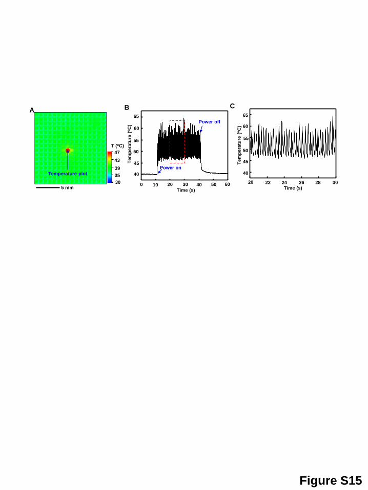
Figure S15
B C
Power on
Tem
pera
ture
(oC
)
Time (s)
0 10 20 30 40 50 60
40
45
50
55
60
65 Power off
Tem
pera
ture
(oC
)
Time (s)
40
45
50
55
60
65
20 22 24 26 28 30
A
5 mm 1 1.5 2 2.5 3 3.5 4 4.5 5
1
1.5
2
2.5
3
3.5
4
4.5
5
data1
30
35
47
39
43
T (oC)
Temperature plot

Dye pixel
PI
Interconnect
A
Dye thickness: 65 mm
Ag thickness: 0.3 mm
Silicon: 600×600 ×1.25 mm3 Au: 600×600×0.3 mm3
PI 9.95 mm
PDMS 100 mm
B
D
t
U
𝒕𝟎
T
U0
Figure S16
820 mm
320 mm
320 mm
100 mm
80 mm
80 mm
C

Max temperature
Min temperatureHeater
Heater Heater
Heater Heater
x (mm)
Tem
pera
ture
(oC
)
0 1000 2000 3000 -1000 -2000 -3000
40
50
60
70
80
90
100
Dye
Ag
Silicon heater Au
PI
PDMS
x
z
O
A
B
Figure S17

Max temperature
Min temperature
0 100 300 400 -100 -200 -300 -400
x (mm)
200
45
50
55
60
65
Tem
pera
ture
(oC
)
PI
Dye
Ag
Silicon heater
Au
PDMS
x O
z
A B
Figure S18

Max temperature
Min temperature
PI
Dye PDMS
z (mm)
0 25 50 75 100 125 150 175 40
50
60
70
80
Tem
pera
ture
(oC
)
A B
Figure S19
PI
Dye
Ag
Silicon heater
Au
PDMS
x O
z

With Ag
Without Ag
100 400 -100 -200 -300 -400
x (mm)
200 0 300 40
50
60
70
80
90
Tem
pera
ture
(oC
)
A B
Figure S20
PI
Dye
Ag
Silicon heater
Au
PDMS
x O
z
Supporting InformationYu et al. 10.1073/pnas.1410494111
Movie S1. Experimental thermal movie of camouflaging of a digital pattern “O.”
Movie S1
Movie S2. FEM thermal movie of camouflaging of a digital pattern “O.”
Movie S2
Yu et al. www.pnas.org/cgi/content/short/1410494111 1 of 2

Movie S3. Movie of dynamic, adaptive pattern recognition and color camouflaging against a moving square background. The video is sped up by three times.
Movie S3
Movie S4. Movie of dynamic, adaptive pattern recognition and color camouflaging on a changing background. The video is sped up by three times.
Movie S4
Other Supporting Information Files
SI Appendix (PDF)
Yu et al. www.pnas.org/cgi/content/short/1410494111 2 of 2