adaptable register file organization for vector processors
TRANSCRIPT

Adaptable Register File Organization for VectorProcessors
Cristobal Ramırez LazoPolytechnic University of Catalonia
and Barcelona Supercomputing CenterBarcelona, Spain
Enrico ReggianiPolytechnic University of Catalonia
and Barcelona Supercomputing CenterBarcelona, Spain
Carlos Rojas MoralesBarcelona Supercomputing Center
Barcelona, [email protected]
Roger Figueras BagueBarcelona Supercomputing Center
Barcelona, [email protected]
Luis Alfonso Villa VargasInstituto Politecnico Nacional
Mexico City, [email protected]
Marco Antonio Ramırez SalinasInstituto Politecnico Nacional
Mexico City, [email protected]
Mateo Valero CortesPolytechnic University of Catalonia
and Barcelona Supercomputing CenterBarcelona, Spain
Osman Sabri UnsalBarcelona Supercomputing Center
Barcelona, [email protected]
Adrian CristalPolytechnic University of Catalonia
and Barcelona Supercomputing CenterBarcelona, Spain
Abstract—Modern scientific applications are getting more di-verse, and the vector lengths in those applications vary widely.Contemporary Vector Processors (VPs) are designed either forshort vector lengths, e.g., Fujitsu A64FX with 512-bit ARM SVEvector support, or long vectors, e.g., NEC Aurora Tsubasa with16Kbits Maximum Vector Length (MVL1). Unfortunately, bothapproaches have drawbacks. On the one hand, short vector lengthVP designs struggle to provide high efficiency for applicationsfeaturing long vectors with high Data Level Parallelism (DLP).On the other hand, long vector VP designs waste resources andunderutilize the Vector Register File (VRF) when executing lowDLP applications with short vector lengths. Therefore, those longvector VP implementations are limited to a specialized subsetof applications, where relatively high DLP must be present toachieve excellent performance with high efficiency. To overcomethese limitations, we propose an Adaptable Vector Architecture(AVA) that leads to having the best of both worlds. AVA isdesigned for short vectors (MVL=16 elements) and is thus areaand energy-efficient. However, AVA has the functionality toreconfigure the MVL, thereby allowing to exploit the benefitsof having a longer vector (up to 128 elements) microarchitecturewhen abundant DLP is present. We model AVA on the gem5simulator and evaluate the performance with six applicationstaken from the RiVEC Benchmark Suite. To obtain area andpower consumption metrics, we model AVA on McPAT for22nm technology. Our results show that by reconfiguring oursmall VRF (8KB) plus our novel issue queue scheme, AVAyields a 2X speedup over the default configuration for shortvectors. Additionally, AVA shows competitive performance whencompared to a long vector VP, while saving 50% of area.
1The Maximum Vector Length (MVL) refers to the maximum number ofelements held in each vector register. MVL is commonly selected at designtime by the computer architect based on the VP target market.
I. INTRODUCTION
Supercomputing has always been instrumental as an initialtesting ground for innovative architectures. Today, Exascalecomputing represents the new milestone for supercomput-ing. To achieve Exascale performance within the 20 MWpower envelope, highly energy-efficient hardware substratesare needed. VPs are a prime candidate for such substratesas they are typically highly energy-efficient, for example, bycomputing on operands composed of vectors instead of scalars,therefore requiring fewer instructions to fetch, or by processingmultiple vector instructions simultaneously through techniquessuch as chaining. In that sense, recent Exascale projectshave shown a renewed interest in vector architectures. Someexamples are the European Processor Initiative (EPI) [1] andthe Japanese Post-K [40] projects. The EPI project proposesa RISC-V based design, aiming to develop power-efficientand high throughput accelerators. On the other hand, in thePost-K project context, Fujitsu put into operation the Fugakusupercomputer, which is currently ranked first in the TOP500list [5]. Fugaku features the Fujitsu ARM A64FX VP, whichadopts the ARM Scalable Vector Extension (SVE) [36] as anefficient way to achieve Exascale-class performance.
Although both the ARM SVE and the RISC-V vectorextensions took inspiration from the more traditional vectorarchitectures, such as the Cray-1 [33], there is a remarkabledifference between them. While ARM SVE allows imple-mentations from 128-bits up to 2048-bits, RISC-V does notlimit the MVL, spacing from short and medium size vectors,to long vector designs, which are akin to classic vector
1
arX
iv:2
111.
0530
1v1
[cs
.AR
] 9
Nov
202
1

supercomputers [8], [21], [33] and modern VPs [7], [39].For example, the Aurora VP from NEC [39] can multiply-accumulate two 256 element double-precision floating-pointvectors in a single instruction.
The vector architectures designed for long vectors arelimited to a specialized subset of applications, where relativelyhigh DLP must be present to achieve excellent performancewith high efficiency. However, scientific applications are get-ting more diverse, and the vector lengths in practical applica-tions vary widely. For example, stencil and graph processingkernels usually feature short vectors, while high-performancecomputing, physics simulation and financial analysis kernelsusually operate on long vectors [31]. We believe that thiswide diversity is one of the main reasons behind the trend ofbuilding parallel machines with short vectors. Short vector de-signs are area efficient and are ”compatible” with applicationshaving long vectors; however, these short vector architecturesare not efficient as longer vector designs when executing highDLP code.
To help to addressing this wide diversity of vector lengths inpractical applications, new vector extensions such as RISC-VV-extension and ARM SVE adopt the Vector Length Agnosticprogramming. In this programming model, the vector lengthis not prescribed as in the common Multimedia SIMD ISAs,allowing the vendor to choose the MVL, while guaranteeingportability of the binary code between different hardwareimplementations. However, since hardware architectures aredesigned to target specific MVLs, designing for only short orlong MVL leads to inefficiencies when trying different DLPpatterns. In this paper, we tackle this challenge by proposing anovel vector architecture that combines the area and resourceefficiency characterizing short VPs with the ability to handlelarge DLP applications, as allowed in long vector architectures.
In this context, we present AVA, an Adaptable VectorArchitecture designed for short vectors (MVL = 16 elements2),capable of reconfiguring the MVL when executing applicationswith abundant DLP, achieving a performance comparable toa native3 design for long vectors. The design is based onthree complementary concepts. First, a two-level renamingscheme based on a new type of registers termed as VirtualVector Registers (VVRs), which are an intermediate mappingbetween the conventional logical and the physical and memoryregisters. In the first level, logical registers are renamed toVVRs, while in the second level, a VRF-Mapping enginekeeps track of which VVRs are mapped to physical registersand which are mapped to memory registers. Second, a two-level VRF, that supports 64 vector registers whose MVLcan be configured from 16 to 128 elements. The first levelcorresponds to the VVRs mapped in the physical registers held
2From now on, one element corresponds to a 64-bit word. Thus, the baselineconfiguration with MVL= 16 elements has a configuration of 1024-bits. Thelarger configuration with MVL= 128 elements has a configuration of 8192-bits.
3Native hardware denotes a vector architecture designed for a specificMVL and is the baseline to compare against in this paper. For example, avector architecture with 64 renamed registers and MVL=128 double precisionelements implies a VRF of 64KB.
in the 8KB Physical Vector Register File (P-VRF), while thesecond level represents the VVRs mapped in memory registersheld in the Memory Vector Register File (M-VRF). While thebaseline configuration (MVL=16 elements) holds all the VVRsin the P-VRF, larger MVL configurations holds a subset ofthe total VVRs in the P-VRF, and maps the remaining partin the M-VRF. Third, we propose a novel two-stage VectorIssue Scheme. In the first stage, the second level of mappingbetween the VVRs and physical registers is performed, whileissuing to execute is managed in the second stage.
Besides the AVA architecture outlined above, the maincontributions of this paper are summarized as follows:
• We demonstrate that AVA improves the performance ofapplications exploiting both low and high DLP, achievinga speedup of up to 2X by reconfiguring the AVA short-vector implementation.
• We show that the 8KB P-VRF AVA configurationachieves comparable performance with respect to theequivalent native implementations, which feature a 64KBVRF.
• We compare AVA with the Register Grouping (RG)feature proposed by the new RISC-V Vector Extension,and we demonstrate that our scheduling technique canproduce fewer swap operations (spill code in RG), per-forming better in most of the evaluated applications.
• We show that AVA adds a negligible 0.55% area over-head, while reducing the total vector processing unit areaby 53% compared with a native design for long vectors.
• We demonstrate that despite generating additional mem-ory traffic, AVA is energy efficient.
• We implement the required AVA support at RTL andintegrate it on a RISC-V based Vector Processing Unit(VPU), including synthesis and place-and-route at 22nm.
This paper is organized as follows: in Section 2, we presentthe background and the motivations behind this work. Insection 3, we detail our AVA model. In Section 4, the eval-uation methodology is shown. The performance, energy andarea results are highlighted in Sections 5 and 6, respectively.In Section 7, synthesis and place-and-route experiments areshown. In section 8, related work is described. Finally, Section9 summarizes the key points of this work.
II. BACKGROUND AND MOTIVATION
An effective way to achieve high performance and efficiencyis to leverage on DLP. In this sense, parallel architecturescan deliver good performance at a lower cost. One categoryof parallel hardware organization is termed Single InstructionMultiple Data (SIMD) [17]. Two variants of SIMD are mul-timedia extensions and vector architectures [20]. Multimediaextensions operate on fixed length vector registers. In contrast,in a Vector Architecture, there is no single preferred vectorlength, just the MVL is defined, and the application can useany vector length that does not exceed the MVL. Nowadays,most commodity CPUs implement architectures that featureSIMD instructions. Common examples for Multimedia exten-sions include Intel x86’s MMX, SSE, AVX, AVX2 and AVX-
2

512 [22], MIPS’s MSA [27], ARM’s NEON [11]. While clas-sical vector extensions for NEC [14] and CRAY [38] are well-known, ”the return of the vectors” includes such contemporaryvector architectures as ARM’s SVE [37], SVE2 [3], and RISC-V V extension [6].
A. Vector architectures
Vector architectures, closely identified with supercomputersdesigned by Seymour Cray [8], [21], [33], represent an elegantinterpretation of SIMD. A key element of these architecturesis that arithmetic/logic and load/store instructions operate onsets of vectors instead of individual data items. Moreover,vector architectures typically exploits long execution pipelinesto obtain good performance at a lower cost. One of themain features of vector architectures is the VRF, composed ofvector registers capable of holding a large number of elements.For these architectures, the maximum number of elements isrepresented by the MVL parameter, which can vary dependingon the hardware implementation [20].
Vector architectures that include multiple lanes can producemultiple results per clock cycle. As shown by Asanovic [12],adding multiple vector processing lanes is an efficient tech-nique that leads to an advantage in performance and scalability.In a multi-lane vector architecture, each lane synchronouslyoperates with a subset of both the VRF and the functionalunit data paths [32]. The VRF usually dominates the area ofa single lane, as reported in Ara [13] and Hwacha [15].
Multi-lane VPs designed for long vectors achieve excellentcomputational throughput and the most efficient execution forprograms with high DLP. However, applications lacking abun-dant DLP are unable to fully utilize the hardware resourcesin the vector lanes. When the Application Vector Length isnotably smaller than the MVL, multiple inefficiencies arise.First, short vector applications cannot fully use each vectorregister width, as a portion of each vector register remainsunderutilized during the whole program execution. Second,when the number of vector registers is not sufficient, the com-piler generates spill code. At compilation time, the compileris not aware of the Application Vector Length. In that sense,the spill code includes load/store of vector registers with theMVL, even though the application only needs a portion ofthem. This behavior could lead to a performance degradationas well as energy waste.
Long vectors bring several advantages such as maximizingthe amount of latency amortized per vector instruction. In thatsense, different ideas have been studied trying to preservemulti-lane VPs designed for long vectors, while being ableto exploit different DLP patterns in an efficient way byreconfiguring the available resources. A couple of the morerepresentative examples for this related work are describedbelow.
Krashinsky et al. proposed the Vector Thread Architec-ture [25], a hybrid multithreaded vector architecture thatprovides a control processor and an array of slave virtualprocessors to the programmer. To execute high DLP code, thecontrol processor can use vector-fetch commands to broadcast
vector instructions to be executed in all virtual processors,where each virtual processor executes a subset of the vectorelements as in the traditional multi-lane designs. On thecontrary, to execute thread-parallel code, each virtual processorcan use thread-fetches to direct its own control flow as anefficient way to execute short vectors.
Rivoire et al. proposed Vector Lane Threading [32], anarchitectural enhancement that allows idle vector lanes to runshort-vector or scalar threads. When running low DLP code,they assign the different lanes across several threads. Then,the combination of threads can saturate the available compu-tational resources. In that sense, the microarchitecture allowsthe exploitation of data-level and thread-level parallelism toachieve higher performance.
While the above approaches also feature some reconfigura-bility, their base VP design targets long vectors, which is costlyin terms of area and resources. In contrast, AVA is centeredaround a design targeting short vectors, which is inherentlyarea and resource-efficient. However, AVA reconfigurabilityenables this short vector design to perform as well as aVP designed for long vectors. Additionally, featuring a smallVRF offers several advantages, such as the opportunity toimplement multi-ported memory structures, a feature that forlarge memory structures could be highly costly in terms ofarea and power, or sometimes prohibited depending on thedesign requirements.
MVL reconfigurability has also been proposed at ISA level.For example, the new RISC-V vector extension [6] includesa novel feature called Register Grouping (RG), whose maingoal is to increase the execution efficiency for applicationsfeaturing high DLP. RG allows grouping multiple vector reg-isters together, so that a single vector instruction can operateon multiple vector registers as if it was a single ”wider”register at the cost of having fewer available architecturalregisters. The Vector Length Multiplier (LMUL) representsthe default number of vector registers that are combined toform a vector register group. Specifically, LMUL supports fourdifferent configurations (i.e., 1,2,4,8). For those values, theMVL can be increased by 1x, 2x, 4x and 8x while reducing thenumber of architectural registers from 32 defined by the vectorISA down to 16, 8 and 4, respectively. It is worth noticingthat when the application needs more architectural registersthan the one available at that time, spill code is generated bythe compiler. The bigger the LMUL configuration, the higherthe probability of generating spill code. When implementingrenaming, physical vector registers are also reduced by LMUL.This implies that for a renaming of 64 physical vector registersfor the LMUL=8 configuration there are only 8 register groupsavailable, 4 assigned initially in the Register Alias Table (RAT)and 4 in the Free Register List (FRL). This leads to acceptingonly four vector instructions before the FRL is empty, and astall occurs in the scalar core.
Similarly, AVA pursuits the same RG goal, which is toprovide the capability to operate on longer vectors whenapplications exhibit abundant DLP. However, AVA allows thisreconfigurability completely at hardware level, preserving the
3
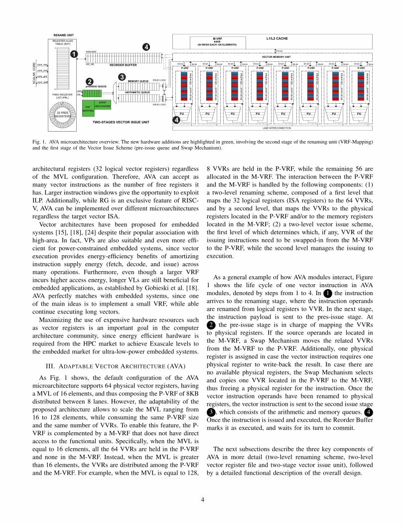
Fig. 1. AVA microarchitecture overview. The new hardware additions are highlighted in green, involving the second stage of the renaming unit (VRF-Mapping)and the first stage of the Vector Issue Scheme (pre-issue queue and Swap Mechanism).
architectural registers (32 logical vector registers) regardlessof the MVL configuration. Therefore, AVA can accept asmany vector instructions as the number of free registers ithas. Larger instruction windows give the opportunity to exploitILP. Additionally, while RG is an exclusive feature of RISC-V, AVA can be implemented over different microarchitecturesregardless the target vector ISA.
Vector architectures have been proposed for embeddedsystems [15], [18], [24] despite their popular association withhigh-area. In fact, VPs are also suitable and even more effi-cient for power-constrained embedded systems, since vectorexecution provides energy-efficiency benefits of amortizinginstruction supply energy (fetch, decode, and issue) acrossmany operations. Furthermore, even though a larger VRFincurs higher access energy, longer VLs are still beneficial forembedded applications, as established by Gobieski et al. [18].AVA perfectly matches with embedded systems, since oneof the main ideas is to implement a small VRF, while ablecontinue executing long vectors.
Maximizing the use of expensive hardware resources suchas vector registers is an important goal in the computerarchitecture community, since energy efficient hardware isrequired from the HPC market to achieve Exascale levels tothe embedded market for ultra-low-power embedded systems.
III. ADAPTABLE VECTOR ARCHITECTURE (AVA)
As Fig. 1 shows, the default configuration of the AVAmicroarchitecture supports 64 physical vector registers, havinga MVL of 16 elements, and thus composing the P-VRF of 8KBdistributed between 8 lanes. However, the adaptability of theproposed architecture allows to scale the MVL ranging from16 to 128 elements, while consuming the same P-VRF sizeand the same number of VVRs. To enable this feature, the P-VRF is complemented by a M-VRF that does not have directaccess to the functional units. Specifically, when the MVL isequal to 16 elements, all the 64 VVRs are held in the P-VRFand none in the M-VRF. Instead, when the MVL is greaterthan 16 elements, the VVRs are distributed among the P-VRFand the M-VRF. For example, when the MVL is equal to 128,
8 VVRs are held in the P-VRF, while the remaining 56 areallocated in the M-VRF. The interaction between the P-VRFand the M-VRF is handled by the following components: (1)a two-level renaming scheme, composed of a first level thatmaps the 32 logical registers (ISA registers) to the 64 VVRs,and by a second level, that maps the VVRs to the physicalregisters located in the P-VRF and/or to the memory registerslocated in the M-VRF; (2) a two-level vector issue scheme,the first level of which determines which, if any, VVR of theissuing instructions need to be swapped-in from the M-VRFto the P-VRF, while the second level manages the issuing toexecution.
As a general example of how AVA modules interact, Figure1 shows the life cycle of one vector instruction in AVAmodules, denoted by steps from 1 to 4. In 1 the instructionarrives to the renaming stage, where the instruction operandsare renamed from logical registers to VVR. In the next stage,the instruction payload is sent to the pres-issue stage. At2 the pre-issue stage is in charge of mapping the VVRs
to physical registers. If the source operands are located inthe M-VRF, a Swap Mechanism moves the related VVRsfrom the M-VRF to the P-VRF. Additionally, one physicalregister is assigned in case the vector instruction requires onephysical register to write-back the result. In case there areno available physical registers, the Swap Mechanism selectsand copies one VVR located in the P-VRF to the M-VRF,thus freeing a physical register for the instruction. Once thevector instruction operands have been renamed to physicalregisters, the vector instruction is sent to the second issue stage3 , which consists of the arithmetic and memory queues. 4
Once the instruction is issued and executed, the Reorder Buffermarks it as executed, and waits for its turn to commit.
The next subsections describe the three key components ofAVA in more detail (two-level renaming scheme, two-levelvector register file and two-stage vector issue unit), followedby a detailed functional description of the overall design.
4
A. Two-level Renaming Scheme: Virtual, Physical and Mem-ory Registers
AVA implements a two-level renaming scheme which isbased on a new type of registers termed as VVRs, which arean intermediate mapping between the logical registgers andthe physical and memory registers.
In the first level, logical registers are renamed to VVRsusing the conventional structures: The RAT, a 6-bit x 32-entries structure in charge of keeping the mapping between thelogical registers and the VVRs, and the FRL which containsthe available VVRs to be assigned as a virtual destination.
Freeing up Virtual Vector Registers. Freeing up VVRs isperformed when an instruction commits. Then, the correspond-ing old destination VVR is sent to the FRL. Additionally, thecorresponding Register Access Counter (RAC) (see sectionIII.C for RAC details ) is set to 0.
In the second level, the VRF-Mapping logic keeps trackof which VVRs are either mapped to physical or memoryregisters. This logic is composed of three simple structures.The First structure is the Physical Register Mapping Table(PRMT), a 6-bit x 64-entries structure in charge of keeping thecorrespondences between the VVRs and the physical registers.The second structure is the Vector Register Location Table(VRLT), a 1-bit x 64-entries structure that indicates if a givenVVR is located in the physical or memory registers. Third, thePhysical Free Register List (PFRL) is a structure that holds theavailable physical registers to be assigned.
Freeing up Physical Registers. The freeing up of a phys-ical register occurs in two distinct cases. (1) AVA exploitsthe concept of aggressive register reclamation [9] to enablephysical register usage to closely match the true lifetime ofregisters. In this sense, it is possible to claim and free aphysical register that will not be longer used. The aggressiveregister reclamation is applied only when: (a) a RAC (seesection III.C for RAC details) counter reaches zero, meaningthat a specific VVR has been renamed, that all the consumershave read the VVR, and that the VVR has become an olddestination of a younger instruction, and (b) there are no oldervector memory instructions in the pipeline. In this scenario,the corresponding physical register assigned to the VVR whichhas its count equal to zero can be pushed to the PFRLstructure. Note that by updating the RAC counters at committime we ensure that the freeing up will not create a conflictin case a recovery event (branch missprediction or exceptionin the scalar pipeline) arises. This is because we are ensuringthat all the instructions that read that VVR has committed. (2)When a physical register for the new instruction is needed,but there is no RAC count with 0. In this case, based on theinformation provided by the RAC counters, it is selected theVVR mapped in the P-VRF which has the lower count, anddoes not matches with any of the instruction virtual sourceoperands, to be sent to the M-VRF and freed the correspondingphysical register.
Contrary to the RISC-V RG proposal where the number oflogical and physical registers are reduced by LMUL factor,
our model allows to preserve the same number of Logical andVVRs no matter if the MVL increases.
B. Two-level Vector Register File
The adaptability of AVA allows to reconfigure the MVLfrom 16 elements up to 128 elements while keeping the samemodest P-VRF size. It is achieved by backing the P-VRF witha second level VRF termed as M-VRF. In this scheme, theVVRs that are being used or close to be used are assignedto the first level (i.e., P-VRF) allowing them to have directaccess to the functional units. On the other hand, the VVRsthat are not being used or will not be used soon are assignedto the second level (i.e., M-VRF). Additionally, each VVR isassociated with one entry of the valid-bit structure (1-bit x 64-entries) which indicates a valid data. When a VVR is assignedat renaming time, the associated Valid-bit is set to 0. Once thevector instruction executes, the associated Valid-bit is set to 1.
Since our baseline microarchitecture features an 8-LaneVPU, the P-VRF is implemented as eight 4R-2W 1-KB (64-bit words x 128 entries) SRAM memory structures distributedbetween the eight lanes. The P-VRF contains 64 physicalregisters where each register is 16 elements wide for thebaseline configuration as illustrated in Figure 1. Note that ourmodel is restricted to execute one arithmetic operation plusone memory operation in parallel. Accordingly, 3 read portsand 1 write port are assigned to the arithmetic pipeline, while1 read port and 1 write port are assigned to the memory unit.Adding more arithmetic pipelines would increase the requiredVRF ports which has a super-linear impact on the power/arearesults as demonstrated by Arima et al. [10] and Zyuban etal [42].
TABLE IPHYSICAL VECTOR REGISTER FILE CONFIGURATIONS.
P-Regs 64 32 21 16 12 10 9 8MVL 16 32 48 64 80 96 112 128
Furthermore, by setting a configuration register, it is pos-sible to configure the VPU for longer MVLs at the costof reducing the number of physical registers that can beheld in the P-VRF. For example, we can configure from 64physical registers (16 elements each), down to 8 physicalregisters (128 elements each) in multiples of 16 elements assummarized in Table I. Note that supporting all the proposedconfigurations does not incur in additional routing overhead.Indeed, the read/write control logic iterates MVL/lanes timesuntil it completes the read/write operation.
When MVL>16 elements, it is needed to reserve therequired memory for holding the M-VRF. In our experiments,we use a custom intrinsic called set virtual vrf (performing amalloc assignment and sending the base address to the VPU)to reserve memory for the M-VRF. However, ideally, the OStakes care of reserving the memory space for each thread.
5
C. Two-stages Vector Issue Unit
The two-stages vector issue unit is composed of the pre-issue stage and the issue stage. We now explain both stagesin turn.
Pre-issue stage: The first level of mapping from LogicalRegisters to VVF occurs in the renaming stage. Pre-issue stageperforms the second level of mapping between the VVRs andphysical registers. As mentioned before, when MVL>16, asubset of the VVRs is held in the P-VRF, while the remainingVVRs are allocated in the M-VRF. In case a new physicalregister is required, but there is not any free physical register,the content of a selected VVR is sent to the M-VRF to freeone physical register, and is assigned to the new instruction.Eventually, VVRs previously moved to the M-VRF can beneeded by a new vector instruction, which then requires tomove the content back to the P-VRF. We term these operationsas Swap operations. In consequence, AVA implements a SWAPMechanism module which is composed of two main structures: the RAC and the Swap Logic. (1) The RAC is a 3-bit x64-entry structure where each entry holds how many timesa specific VVR is read. At the first stage of the renaming,the RAC counters are updated. First, the new destinationand source VVRs increment the corresponding register count,while the old destination VVR decrements the correspondingcount. At commit time, the counters are updated again. Thistime, the source VVRs decrement the corresponding counter.The RAC helps to take decisions based on the count of eachindividual VRR which are described in the next paragraphs. (2)The Swap Logic decides which VVRs should be swapped tothe M-VRF, and creates memory operations termed as Swap-Stores. Swap Logic also decides when it is required to moveVVRs from the M-VRF to the P-VRF, and creates operationstermed as Swap-Loads. The Swap Logic takes advantage ofthe information provided by the RAC counters to decide whichVVR allocated in the P-VRF should be swapped to the M-VRF. This selection is based on the VVR mapped in the P-VRF which has the lower count (1 is the lowest count forswaps, and 0 is the count for aggressive register reclamation),and selection logic also checks that the candidate VVR doesnot match with any of the instruction virtual source operandsto avoid deadlock.
Pre-issue stage implements an in-order issue scheme. Avector instruction is ready to be issued to the second levelonly when it has been fully renamed from VVRs to physicalregisters. However, renaming the instruction from VVRs tophysical registers implies several steps evaluated in the fol-lowing order:
(A) Source VVRs are mapped to the corresponding physicalregister by reading the PRMT and the VRLT structures (in-dexed by the source VVRs). There are two possible scenariosfor each source operand: (1) If the value read from the VRLTis equal to ”1”, indicates that the physical register obtainedfrom the PRMT structure is valid and it is located in theP-VRF, and the corresponding source VVR can be mappedimmediately. (2) On the contrary, if the value read from the
VRLT is equal to ”0”, the VVR is located in the M-VRF andis loaded to the P-VRF to be used. In this second scenario,it is required to notify the conflict to the Swap Mechanism.A couple of tasks are performed by the Swap Mechanism:(Swap-1) Verifies that there is at least one physical registeravailable to load the values from the M-VRF. In case thereare not free physical registers, a Swap-Store is created andsent to the Memory queue to store the content of one VVRselected by the Swap Logic from the P-VRF to the M-VRF.With this, the associated physical register can be freed andpushed to the PFRL. (Swap-2) Then, a Swap-Load is createdand sent to the Memory queue to load the VVR from theM-VRF to the P-VRF.
(B) If the vector instruction requires to write-back its result,a new physical register must be assigned. In case there areno free physical registers, the task Swap-1 must be repeated.Then, the new available physical register can be assigned asthe physical destination.
(C) Finally, once the instruction has been renamed, it isissued to the second level only if there is availability in theircorresponding queue. Otherwise, a stall is signaled until thereis at least one free slot for the instruction.
Issue stage: it is composed of the Memory and ArithmeticQueues in charge of issuing the vector instruction. Individu-ally each queue performs in-order issue, however, since thememory queue is decoupled from the Arithmetic queue, thereis a light out-of-order behaviour. Because of the introductionof Swap Operations, AVA must guarantee for each instructioneither in the Arithmetic or Memory Queue to have its sourceVVRs mapped to the P-VRF when it is its turn to be issuedto execute, avoiding deadlocks. This is done by following 2rules: (1) Swap-Stores created to free one physical registermust notify to the new owner of the physical register that ithas executed, meaning that the VVR previously mapped in thephysical register is now in the M-VRF, and then it is possibleto write-back new data to the physical register. (2) Swap-Loadsmust wait to all the consumers of the previously VVR mappedin P-VRF have read the register.
Once the instruction is issued and executed, it will bemarked in the reorder-buffer as executed, only waiting for itsturn to commit.
D. Recovering the microarchitectural stateAfter some event such as a miss-prediction or memory ex-
ceptions, AVA can roll back and recover the microarchitecturestate. The renaming tables (RAT and FRL pointers) and theValid-bit are the only mandatory structures to be recovered.Therefore, AVA implements only one copy that is updatedevery time a vector instruction commits.
Recovering the RAC counters is optional, since every timethat a VVR is freed, the respective count is also set to zero.Thus, not recovering the state of the counters does not implyany correctness issue.
E. AVA Functional DescriptionFig. 2 illustrates the AVA functional behavior based on the
execution of three instructions. The selected MVL configura-
6
4041
64-b
it w
ord
* 12
8 en
trie
s
RA
TF
RL
RENAME UNITVRF MAPPING
PF
RL
LA
NE
1
5
000
PR
MT
VR
LT
RA
C
P-V
RF
ALU
2
43
1
6
000
3839
... ... ...1
3
1
2
2
3
... 424344456362
TAIL HEAD
123
374344
42
...
TAIL HEAD
123
XXXXXX
2
1
SWAPLOGIC
1
0
63
4
6X
3
3,7
3
PRE-ISSUE STAGESWAP MECH
2351 301 31
363738 1 13
1 2739
074443 03
06421 251 44
...62
X
XX
XX
00
01
111
000
111
... ...
2
1
2
33
2
22
0
78
...
31
1example code:
3
vle.v v4 (@v1)
vle.v v5 (@v2)
vfadd.v v6 v5 v4
2
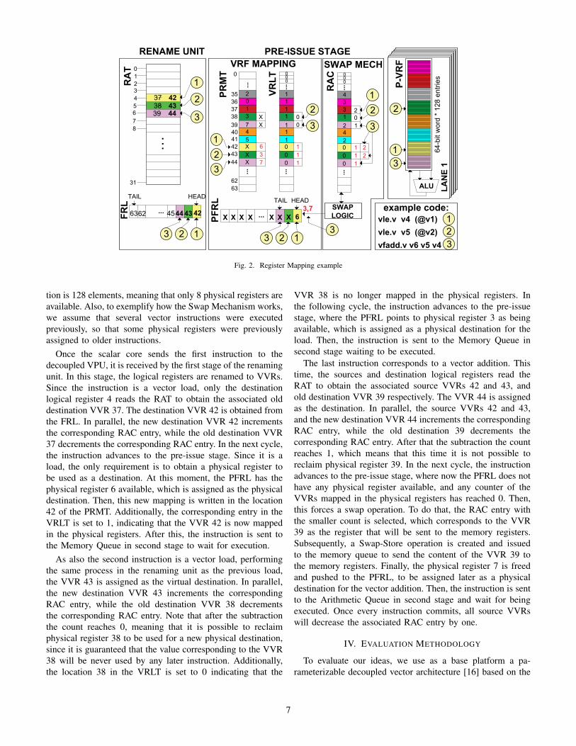
Fig. 2. Register Mapping example
tion is 128 elements, meaning that only 8 physical registers areavailable. Also, to exemplify how the Swap Mechanism works,we assume that several vector instructions were executedpreviously, so that some physical registers were previouslyassigned to older instructions.
Once the scalar core sends the first instruction to thedecoupled VPU, it is received by the first stage of the renamingunit. In this stage, the logical registers are renamed to VVRs.Since the instruction is a vector load, only the destinationlogical register 4 reads the RAT to obtain the associated olddestination VVR 37. The destination VVR 42 is obtained fromthe FRL. In parallel, the new destination VVR 42 incrementsthe corresponding RAC entry, while the old destination VVR37 decrements the corresponding RAC entry. In the next cycle,the instruction advances to the pre-issue stage. Since it is aload, the only requirement is to obtain a physical register tobe used as a destination. At this moment, the PFRL has thephysical register 6 available, which is assigned as the physicaldestination. Then, this new mapping is written in the location42 of the PRMT. Additionally, the corresponding entry in theVRLT is set to 1, indicating that the VVR 42 is now mappedin the physical registers. After this, the instruction is sent tothe Memory Queue in second stage to wait for execution.
As also the second instruction is a vector load, performingthe same process in the renaming unit as the previous load,the VVR 43 is assigned as the virtual destination. In parallel,the new destination VVR 43 increments the correspondingRAC entry, while the old destination VVR 38 decrementsthe corresponding RAC entry. Note that after the subtractionthe count reaches 0, meaning that it is possible to reclaimphysical register 38 to be used for a new physical destination,since it is guaranteed that the value corresponding to the VVR38 will be never used by any later instruction. Additionally,the location 38 in the VRLT is set to 0 indicating that the
VVR 38 is no longer mapped in the physical registers. Inthe following cycle, the instruction advances to the pre-issuestage, where the PFRL points to physical register 3 as beingavailable, which is assigned as a physical destination for theload. Then, the instruction is sent to the Memory Queue insecond stage waiting to be executed.
The last instruction corresponds to a vector addition. Thistime, the sources and destination logical registers read theRAT to obtain the associated source VVRs 42 and 43, andold destination VVR 39 respectively. The VVR 44 is assignedas the destination. In parallel, the source VVRs 42 and 43,and the new destination VVR 44 increments the correspondingRAC entry, while the old destination 39 decrements thecorresponding RAC entry. After that the subtraction the countreaches 1, which means that this time it is not possible toreclaim physical register 39. In the next cycle, the instructionadvances to the pre-issue stage, where now the PFRL does nothave any physical register available, and any counter of theVVRs mapped in the physical registers has reached 0. Then,this forces a swap operation. To do that, the RAC entry withthe smaller count is selected, which corresponds to the VVR39 as the register that will be sent to the memory registers.Subsequently, a Swap-Store operation is created and issuedto the memory queue to send the content of the VVR 39 tothe memory registers. Finally, the physical register 7 is freedand pushed to the PFRL, to be assigned later as a physicaldestination for the vector addition. Then, the instruction is sentto the Arithmetic Queue in second stage and wait for beingexecuted. Once every instruction commits, all source VVRswill decrease the associated RAC entry by one.
IV. EVALUATION METHODOLOGY
To evaluate our ideas, we use as a base platform a pa-rameterizable decoupled vector architecture [16] based on the
7
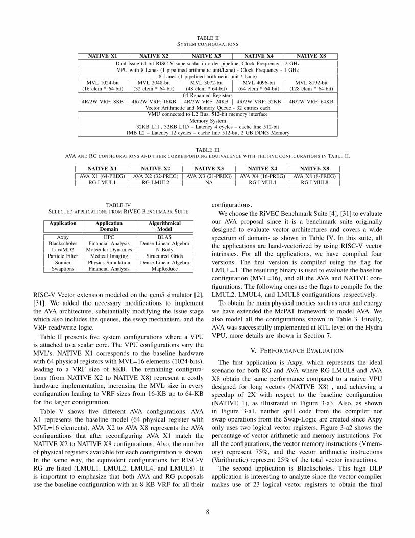
TABLE IISYSTEM CONFIGURATIONS
NATIVE X1 NATIVE X2 NATIVE X3 NATIVE X4 NATIVE X8Dual-Issue 64-bit RISC-V superscalar in-order pipeline, Clock Frequency - 2 GHzVPU with 8 Lanes (1 pipelined arithmetic unit/Lane) - Clock Frequency - 1 GHz
8 Lanes (1 pipelined arithmetic unit / Lane)MVL 1024-bit MVL 2048-bit MVL 3072-bit MVL 4096-bit MVL 8192-bit
(16 elem * 64-bit) (32 elem * 64-bit) (48 elem * 64-bit) (64 elem * 64-bit) (128 elem * 64-bit)64 Renamed Registers
4R/2W VRF: 8KB 4R/2W VRF: 16KB 4R/2W VRF: 24KB 4R/2W VRF: 32KB 4R/2W VRF: 64KBVector Arithmetic and Memory Queue - 32 entries eachVMU connected to L2 Bus, 512-bit memory interface
Memory System32KB L1I , 32KB L1D – Latency 4 cycles – cache line 512-bit
1MB L2 – Latency 12 cycles – cache line 512-bit, 2 GB DDR3 Memory
TABLE IIIAVA AND RG CONFIGURATIONS AND THEIR CORRESPONDING EQUIVALENCE WITH THE FIVE CONFIGURATIONS IN TABLE II.
NATIVE X1 NATIVE X2 NATIVE X3 NATIVE X4 NATIVE X8AVA X1 (64-PREG) AVA X2 (32-PREG) AVA X3 (21-PREG) AVA X4 (16-PREG) AVA X8 (8-PREG)
RG-LMUL1 RG-LMUL2 NA RG-LMUL4 RG-LMUL8
TABLE IVSELECTED APPLICATIONS FROM RIVEC BENCHMARK SUITE
Application Application AlgorithmicalDomain Model
Axpy HPC BLASBlackscholes Financial Analysis Dense Linear Algebra
LavaMD2 Molecular Dynamics N-BodyParticle Filter Medical Imaging Structured Grids
Somier Physics Simulation Dense Linear AlgebraSwaptions Financial Analysis MapReduce
RISC-V Vector extension modeled on the gem5 simulator [2],[31]. We added the necessary modifications to implementthe AVA architecture, substantially modifying the issue stagewhich also includes the queues, the swap mechanism, and theVRF read/write logic.
Table II presents five system configurations where a VPUis attached to a scalar core. The VPU configurations vary theMVL’s. NATIVE X1 corresponds to the baseline hardwarewith 64 physical registers with MVL=16 elements (1024-bits),leading to a VRF size of 8KB. The remaining configura-tions (from NATIVE X2 to NATIVE X8) represent a costlyhardware implementation, increasing the MVL size in everyconfiguration leading to VRF sizes from 16-KB up to 64-KBfor the larger configuration.
Table V shows five different AVA configurations. AVAX1 represents the baseline model (64 physical register withMVL=16 elements). AVA X2 to AVA X8 represents the AVAconfigurations that after reconfiguring AVA X1 match theNATIVE X2 to NATIVE X8 configurations. Also, the numberof physical registers available for each configuration is shown.In the same way, the equivalent configurations for RISC-VRG are listed (LMUL1, LMUL2, LMUL4, and LMUL8). Itis important to emphasize that both AVA and RG proposalsuse the baseline configuration with an 8-KB VRF for all their
configurations.We choose the RiVEC Benchmark Suite [4], [31] to evaluate
our AVA proposal since it is a benchmark suite originallydesigned to evaluate vector architectures and covers a widespectrum of domains as shown in Table IV. In this suite, allthe applications are hand-vectorized by using RISC-V vectorintrinsics. For all the applications, we have compiled fourversions. The first version is compiled using the flag forLMUL=1. The resulting binary is used to evaluate the baselineconfiguration (MVL=16), and all the AVA and NATIVE con-figurations. The following ones use the flags to compile for theLMUL2, LMUL4, and LMUL8 configurations respectively.
To obtain the main physical metrics such as area and energywe have extended the McPAT framework to model AVA. Wealso model all the configurations shown in Table 3. Finally,AVA was successfully implemented at RTL level on the HydraVPU, more details are shown in Section 7.
V. PERFORMANCE EVALUATION
The first application is Axpy, which represents the idealscenario for both RG and AVA where RG-LMUL8 and AVAX8 obtain the same performance compared to a native VPUdesigned for long vectors (NATIVE X8) , and achieving aspeedup of 2X with respect to the baseline configuration(NATIVE 1), as illustrated in Figure 3-a3. Also, as shownin Figure 3-a1, neither spill code from the compiler norswap operations from the Swap-Logic are created since Axpyonly uses two logical vector registers. Figure 3-a2 shows thepercentage of vector arithmetic and memory instructions. Forall the configurations, the vector memory instructions (Vmem-ory) represent 75%, and the vector arithmetic instructions(Varithmetic) represent 25% of the total vector instructions.
The second application is Blackscholes. This high DLPapplication is interesting to analyze since the vector compilermakes use of 23 logical vector registers to obtain the final
8

a1) a2) a3) a4)
b1) b2) b3) b4)
c1) c2) c3) c4)
0.20
0.20
0.20
0.15
0.15
0.15
0.12
0.12
0.10
0.10
0.10
0.10
0.10
0.10
1.00
1.00
1.00
1.34
1.34
1.34 1.
63
1.63 1.
95
1.95
1.95 2.03
2.03
2.03
0
0.5
1
1.5
2
2.5
0.00
0.05
0.10
0.15
0.20
0.25
Spee
du
p
Exec
u�
on
Tim
e (s
ecs)
0.E+005.E+051.E+062.E+062.E+063.E+063.E+064.E+06
Mem
ory
Inst
ruc�
on
sVLoad Vstore Spill-Load
Spill-Store SWAP-Load SWAP-Store
0%
20%
40%
60%
80%
100%
% o
f V
ecto
r In
stru
c�o
ns
Varithme�c Vmemory
0
2
4
6
8
10
12
Ener
gy (
mJ)
L2 Dynamic L2 Leakage VRF DynamicVRF Leakage FPU Dynamic FPU Leakage
0.36
0.36
0.36
0.23
0.24
0.23
0.20
0.21
0.18
0.22
0.21
0.15
0.24
0.22
1.00
1.00
1.00
1.58
1.49 1.58 1.
78
1.72 2.
02
1.67 1.71
2.37
1.49 1.
64
0
0.5
1
1.5
2
2.5
0.000.050.100.150.200.250.300.350.40
Spee
du
p
Exec
u�
on
Tim
e (s
ecs)
0.E+005.E+051.E+062.E+062.E+063.E+063.E+064.E+06
Mem
ory
Inst
ruc�
on
s
0%
20%
40%
60%
80%
100%
% o
f V
ecto
r In
stru
c�o
ns
0102030405060708090
Ener
gy (
mJ)
2.44
2.44
2.44
2.01
2.01
2.01
1.46
1.46
1.48
2.23
1.57
1.67
5.04
2.40
1.00
1.00
1.00 1.
22
1.22
1.22
1.67
1.67
1.65
1.09
1.56
1.46
0.48
1.02
00.20.40.60.811.21.41.61.8
0.001.00
2.00
3.00
4.00
5.00
6.00
Spee
du
p
Exec
u�
on
Tim
e (s
ecs)
0.E+00
2.E+07
4.E+07
6.E+07
8.E+07
1.E+08
1.E+08
Mem
ory
Inst
ruc�
on
s
0%
20%
40%
60%
80%
100%
% o
f V
ecto
r In
stru
c�o
ns
0
200
400
600
800
1000
1200
Ener
gy (
mJ)
LavaMD2
Axpy
Blackscholes
3.21
3.21
3.21
2.32
2.32
2.32
2.03
2.03
1.88
1.88
1.88
1.66
1.66
1.67
1.00
1.00
1.00
1.38
1.38
1.38 1.
58
1.58 1.
70
1.70
1.70 1.
93
1.93
1.92
0
0.5
1
1.5
2
2.5
0.000.501.00
1.50
2.002.503.00
3.50
Spee
du
p
Exec
u�
on
Tim
e(s
ecs)
0.E+002.E+044.E+046.E+048.E+041.E+051.E+051.E+05
Mem
ory
Inst
ruc�
on
s
0%
20%
40%
60%
80%
100%
% o
f V
ecto
r In
stru
c�o
ns
0
100
200
300
400
500
600
Ener
gy (
mJ)
d1) d2) d3) d4)
2.25
2.25
2.25
1.78
1.78
1.78
1.77
1.77
1.65
1.65
1.65
1.58
1.82
1.77
1.00
1.00
1.00
1.26
1.26
1.26
1.27
1.27 1.
36
1.36
1.36
1.43
1.23 1.27
00.20.40.60.811.21.41.6
0.00
0.50
1.00
1.50
2.00
2.50
Spee
du
p
Exec
u�
on
Tim
e (s
ecs)
0.E+00
5.E+06
1.E+07
2.E+07
2.E+07
3.E+07
3.E+07
Mem
ory
Inst
ruc�
on
s
0%
20%
40%
60%
80%
100%
% o
f V
ecto
r In
stru
c�o
ns
020406080
100120140160
Ener
gy (
mJ)
e1) e2) e3) e4)
Somier
Particlefilter
2.86
2.86
2.86
2.00
2.05
2.03
1.70
1.84
1.55
1.73
1.72
1.33
1.73
1.61
1.00
1.00
1.00
1.43
1.40
1.41 1.
68
1.56 1.
85
1.66
1.67
2.15
1.66 1.
78
0
0.5
1
1.5
2
2.5
0.000.501.001.50
2.00
2.503.003.50
Spee
du
p
Exec
u�
on
Tim
e (s
ecs)
0.E+00
1.E+07
2.E+07
3.E+07
4.E+07
5.E+07
6.E+07
Mem
ory
Inst
ruc�
on
s
0%
20%
40%
60%
80%
100%
% o
f V
ecto
r In
stru
c�o
ns
0100200300400500600700800
Ener
gy (
mJ)
f1) f2) f3) f4)
Swaptions
NAT
IVE
X1
AV
A X
1
NAT
IVE
X2
AV
A X
2
AV
A X
3
NAT
IVE
X4
AV
A X
4
NAT
IVE
X8
AV
A X
8
NA
TIV
E X
1
AV
A X
1
NA
TIV
E X
2
AV
A X
2
Na�
ve X
3
AV
A X
3
NA
TIV
E X
4
AV
A X
4
NA
TIV
E X
8
AV
A X
8
NA
TIV
E X
1
AV
A X
1
NA
TIV
E X
2
AV
A X
2
AV
A X
3
NA
TIV
E X
4
AV
A X
4
NA
TIV
E X
8
AV
A X
8
NAT
IVE
X1
RG
-LM
UL1
AV
A X
1
NAT
IVE
X2
RG
-LM
UL2
AV
A X
2
NAT
IVE
X3
NAT
IVE
X3
AV
A X
3
NAT
IVE
X4
RG
-LM
UL4
AV
A X
4
NAT
IVE
X8
RG
-LM
UL8
AV
A X
8
NAT
IVE
X3
RG
-LM
UL1
RG
-LM
UL2
RG
-LM
UL4
RG
-LM
UL8
RG
-LM
UL1
RG
-LM
UL2
RG
-LM
UL4
RG
-LM
UL8
RG
-LM
UL1
RG
-LM
UL2
RG
-LM
UL4
RG
-LM
UL8
NAT
IVE
X1
AV
A X
1
NAT
IVE
X2
AV
A X
2
AV
A X
3
NAT
IVE
X4
AV
A X
4
NAT
IVE
X8
AV
A X
8
NAT
IVE
X1
AV
A X
1
NAT
IVE
X2
AV
A X
2
Na�
ve X
3
AV
A X
3
NAT
IVE
X4
AV
A X
4
NAT
IVE
X8
AV
A X
8
NAT
IVE
X1
AV
A X
1
NAT
IVE
X2
AV
A X
2
AV
A X
3
NAT
IVE
X4
AV
A X
4
NAT
IVE
X8
AV
A X
8
NAT
IVE
X1
RG
-LM
UL1
AV
A X
1
NAT
IVE
X2
RG
-LM
UL2
AV
A X
2
NAT
IVE
X3
NAT
IVE
X3
AV
A X
3
NAT
IVE
X4
RG
-LM
UL4
AV
A X
4
NAT
IVE
X8
RG
-LM
UL8
AV
A X
8
NAT
IVE
X3
RG
-LM
UL1
RG
-LM
UL2
RG
-LM
UL4
RG
-LM
UL8
RG
-LM
UL1
RG
-LM
UL2
RG
-LM
UL4
RG
-LM
UL8
RG
-LM
UL1
RG
-LM
UL2
RG
-LM
UL4
RG
-LM
UL8
NAT
IVE
X1
AV
A X
1
NAT
IVE
X2
AV
A X
2
AV
A X
3
NAT
IVE
X4
AV
A X
4
NAT
IVE
X8
AV
A X
8
NA
TIV
E X
1
AV
A X
1
NA
TIV
E X
2
AV
A X
2
Na�
ve X
3
AV
A X
3
NA
TIV
E X
4
AV
A X
4
NA
TIV
E X
8
AV
A X
8
NAT
IVE
X1
AV
A X
1
NAT
IVE
X2
AV
A X
2
AV
A X
3
NAT
IVE
X4
AV
A X
4
NAT
IVE
X8
AV
A X
8
NAT
IVE
X1
RG
-LM
UL1
AV
A X
1
NAT
IVE
X2
RG
-LM
UL2
AV
A X
2
NAT
IVE
X3
NA
TIV
E X
3
AV
A X
3
NAT
IVE
X4
RG
-LM
UL4
AV
A X
4
NAT
IVE
X8
RG
-LM
UL8
AV
A X
8
NAT
IVE
X3
RG
-LM
UL1
RG
-LM
UL2
RG
-LM
UL4
RG
-LM
UL8
RG
-LM
UL1
RG
-LM
UL2
RG
-LM
UL4
RG
-LM
UL8
RG
-LM
UL1
RG
-LM
UL2
RG
-LM
UL4
RG
-LM
UL8
NAT
IVE
X1
AV
A X
1
NAT
IVE
X2
AV
A X
2
AV
A X
3
NAT
IVE
X4
AV
A X
4
NAT
IVE
X8
AV
A X
8
NAT
IVE
X1
AV
A X
1
NAT
IVE
X2
AV
A X
2
Na�
ve X
3
AV
A X
3
NAT
IVE
X4
AV
A X
4
NAT
IVE
X8
AV
A X
8
NAT
IVE
X1
AV
A X
1
NAT
IVE
X2
AV
A X
2
AV
A X
3
NAT
IVE
X4
AV
A X
4
NAT
IVE
X8
AV
A X
8
NAT
IVE
X1
RG
-LM
UL1
AV
A X
1
NAT
IVE
X2
RG
-LM
UL2
AV
A X
2
NAT
IVE
X3
NAT
IVE
X3
AV
A X
3
NAT
IVE
X4
RG
-LM
UL4
AV
A X
4
NAT
IVE
X8
RG
-LM
UL8
AV
A X
8
NAT
IVE
X3
RG
-LM
UL1
RG
-LM
UL2
RG
-LM
UL4
RG
-LM
UL8
RG
-LM
UL1
RG
-LM
UL2
RG
-LM
UL4
RG
-LM
UL8
RG
-LM
UL1
RG
-LM
UL2
RG
-LM
UL4
RG
-LM
UL8
NAT
IVE
X1
AV
A X
1
NAT
IVE
X2
AV
A X
2
AV
A X
3
NAT
IVE
X4
AV
A X
4
NAT
IVE
X8
AV
A X
8
NAT
IVE
X1
AV
A X
1
NAT
IVE
X2
AV
A X
2
Na�
ve X
3
AV
A X
3
NAT
IVE
X4
AV
A X
4
NAT
IVE
X8
AV
A X
8
NAT
IVE
X1
AV
A X
1
NAT
IVE
X2
AV
A X
2
AV
A X
3
NAT
IVE
X4
AV
A X
4
NAT
IVE
X8
AV
A X
8
NAT
IVE
X1
RG
-LM
UL1
AV
A X
1
NAT
IVE
X2
RG
-LM
UL2
AV
A X
2
NAT
IVE
X3
NAT
IVE
X3
AV
A X
3
NAT
IVE
X4
RG
-LM
UL4
AV
A X
4
NAT
IVE
X8
RG
-LM
UL8
AV
A X
8
NA
TIV
E X
3
RG
-LM
UL1
RG
-LM
UL2
RG
-LM
UL4
RG
-LM
UL8
RG
-LM
UL1
RG
-LM
UL2
RG
-LM
UL4
RG
-LM
UL8
RG
-LM
UL1
RG
-LM
UL2
RG
-LM
UL4
RG
-LM
UL8
NAT
IVE
X1
AV
A X
1
NAT
IVE
X2
AV
A X
2
AV
A X
3
NAT
IVE
X4
AV
A X
4
NAT
IVE
X8
AV
A X
8
NAT
IVE
X1
AV
A X
1
NAT
IVE
X2
AV
A X
2
Na�
ve X
3
AV
A X
3
NAT
IVE
X4
AV
A X
4
NAT
IVE
X8
AV
A X
8
NAT
IVE
X1
AV
A X
1
NAT
IVE
X2
AV
A X
2
AV
A X
3
NAT
IVE
X4
AV
A X
4
NAT
IVE
X8
AV
A X
8
NAT
IVE
X1
RG
-LM
UL1
AV
A X
1
NAT
IVE
X2
RG
-LM
UL2
AV
A X
2
NAT
IVE
X3
NAT
IVE
X3
AV
A X
3
NAT
IVE
X4
RG
-LM
UL4
AV
A X
4
NAT
IVE
X8
RG
-LM
UL8
AV
A X
8
NA
TIV
E X
3
RG
-LM
UL1
RG
-LM
UL2
RG
-LM
UL4
RG
-LM
UL8
RG
-LM
UL1
RG
-LM
UL2
RG
-LM
UL4
RG
-LM
UL8
RG
-LM
UL1
RG
-LM
UL2
RG
-LM
UL4
RG
-LM
UL8
Fig. 3. Performance evaluation for the six applications: a)Axpy; b)Blackscholes; c) LavaMD2; d) Particle-Filter; e)Somier; f)Swaptions. Charts in the firstcolumn shows the Vector Memory Instruction count including SPILL operations generated by the compiler and SWAP operations generated by AVA. Charts onthe second column shows the % of vector instruction, charts on the third column shows the Execution-time and Speedup when comparing versus NATIVE-1(baseline), and charts on the fourth column shows the Energy consumption obtained from McPAT.
binary. At first glance, we can see that there is high pressurein the use of vector logical registers. For LMUL=2,4 and 8,the compiler can make use of only 16,8 and 4 logical vectorregisters respectively, and for any of those configurations,spill code is added as shown in Figure 3-b1. AVA presentsa similar behavior. However, it is interesting to see thatfor AVA X2 there are no swap operations. This is becausethe scheduling is done using 32 physical vector registers,meaning that we have enough vector registers to compute
the application without generating swap operations. On theother hand, swap operations are generated starting from theAVA X4. Also, the number of swap operations is slightly lessthan the number of spill code operations generated by thecompiler. This is because AVA performs the scheduling basedon the available physical registers, which are always doublecompared to LMUL. Figure 3-b3 shows the performanceresults. For AVA-X2 there are not swap operations, thus asimilar performance to NATIVE-2 is achieved, and a speedup
9

of 1.58X over the baseline configuration. AVA X4 achieves aspeedup of 1.71X over the baseline configuration. For AVAX8, the percentage of memory operations represents 38%of the total vector instructions, causing a slight performancedegradation (1.64X) because of the increased number of swapoperations. For all the configurations AVA performs better thanRG since less memory traffic is generated.
For LavaMD2, the vector compiler uses 15 logical vectorregisters to create the final binary, which implies that forRG-LMUL2, no spill code is necessary. However, for RG-LMUL4 and RG-LMUL8, spill code is generated as shownin Figure 3-c1, causing an increase in memory operationsfrom 9% for RG-LMUL1 configuration, to up to 43% forRG-LMUL8 configuration as shown in Figure 3-c2. For AVA,the SWAPS operations are few compared with the equivalentspill code generated by the RG-LMUL configuration. Figure3-c3 shows the performance results. First, this applicationmakes use of a fixed vector size of 48 elements, meaning thatfor the configurations with a larger MVL than 48 elementswe cannot make full use of each vector register, and aportion of each vector register remains unused during all theprogram execution. For AVA the best configuration is AVAX3. AVA X3 not only executes the 48 elements with onlyone instruction, but also 21 physical registers are available forthe computation, thereby avoiding swap operations, as shownin Figure 3-c1. Also, it achieves a speedup of 1.67X, betterthan any of the RG- LMUL configurations and equal to theequivalent NATIVE configuration, as shown in Figure 3-c3.Finally, another interesting result is for RG-LMUL8, wherethe performance decrease notably. The reason is because forthis configuration, the memory operations represent 43% ofthe overall vector instructions. Also, 81% of the memoryoperations are spill code. As described in Section 3.1, thespill code is always executed using the MVL. As a result,the memory operations become the bottleneck since all thearithmetic operations (57%) are executed with VL=48, whilespill code is executed with VL=MVL=128.
For Particle-Filter, the compiler requires 13 logical vectorregisters to generate the final binary, which implies that forRG-LMUL2, AVA X2, and AVA X3, no spill/swap operationsare added. On the other hand, spill/swap operations are gen-erated for RG-LMUL4, RG-LMUL8, AVA X4, and AVA X8,as shown in Figure 3-d1. However, the increase in memoryoperations percentage is negligible, representing 0.15% for thelarger configuration, achieving similar performance levels asthe corresponding NATIVE configuration as shown in Figure3-d3.
For Somier, the vector compiler uses 13 logical vectorregisters to generate the final binary. Spill/swap operationsare generated only for RG-LMUL8 and AVA X8. For RG-LMUL8 there was an increase in the percentage of memoryoperations from 46% to 68% as shown in Figure 3-e2. For AVAX8, few swap operations were generated. Figure 3-e3 showsthe performance results. In this case, the NATIVE X4, RG-LMUL4, and AVA X4 achieves the best speedup with 1.43X.For AVA X8 and RG-LMUL8 there was a small performance
degradation because of the additional memory traffic.Finally, for Swaptions, the vector compiler uses 24 logical
vector registers to generate the final binary, which implies thatfor RG-LMUL2, RG-LMUL4, and RG-LMUL8 spill code isgenerated as shown in Figure 3-f1, causing an increase in thepercentage of memory operations from 12% in the NATIVE-1configuration up to 34% in the RG-LMUL8 configuration asshown in Figure 3-f2. For AVA, the swap operations appearstarting from AVA X3, obtaining almost the same number asthe compiler generated spill code for RG. AVA-8 achieves aspeedup of 1.78X while the NATIVE-8 configuration achieves2.15X with respect to the NATIVE-1 configuration.
As shown above, AVA provides performance improvementsfor all the evaluated applications, being competitive withNATIVE designs for longer vectors.
VI. MCPAT AREA AND ENERGY EVALUATION
To demonstrate the area efficiency of AVA, we modeledAVA and the five NATIVE configurations presented in Table 3on the McPAT framework for 22nm technology. Figure 4 (leftaxis) shows the area results for all the VPU configurationspresented in Table 3. We also include the area of the scalarcore including L1I and L1D caches, and the 1MB L2 cache.AVA structures add a negligible 0.55% area overhead to theVPU, while reducing the total VPU area by 53% comparedwith the NATIVE X8 configuration.
0.18 0.18 0.35 0.53 0.70
1.410.94 0.940.94
0.940.94
0.94
1.04
0.140.29 2.460.0061
0.90
1.06 1.09 1.070.81
0.90
1.22 1.41 1.491.44
0
0.1
0.3
0.5
0.7
0.9
1.1
1.3
1.5
0.0
0.5
1.0
1.5
2.0
2.5
3.0
NATIVEX1
AVA NATIVEX2
NATIVEX3
NATIVEX4
NATIVEX8
Core L2Cache
Per
form
ance
/mm
2
Are
a (m
m2 )
VPU VRF VPU FPUs Core pipelineL1-I L1-D L2 CacheAVA structures NATIVE perf/mm2 AVA perf/mm2
Fig. 4. Area results obtained from McPAT for 22nm technology node, andaverage performance/mm2 for each configuration.
To demonstrate the AVA performance/mm2 efficiency, weobtain the average performance for all the previous evaluatedapplications for NATIVE and AVA configurations, and dividedbetween the area for the corresponding configuration. Resultsare shown in Figure 4 (right axis). Note that for AVA, the areais 1.126mm2 for all the configurations.
To demonstrate that AVA is energy efficient, we also obtainthe Energy consumption for all the previous evaluated appli-cations. Last column (left axis) of Figure 3 shows the energyconsumption results. The application statistics introduced inthe McPAT model corresponds to the gem5 outputs. Dynamicand leakage energy results are reported only for the maincontributors: The L2 cache, the VRF and the FPUs.
The required AVA structures also are modeled, however itrepresents only 0.4% of the overall VPU energy consumption
10

for the AVA X1 configuration. Since the number of issuedinstructions is reduced as the MVL value is increased, theenergy consumed by the required AVA structures is alsoreduced for larger MVL configurations. Then, we include theextra energy dissipation of AVA in the VRF Dynamic/Leakagebars for all the AVA configurations.
Axpy (Figure 3-a4) and Particle-Filter (Figure 3-c4) showsa similar behavior since there are either no or few spill/swapoperations. For both, as the MVL is increased, less totalenergy is consumed. Dynamic energy is constant since nospill/swap operations are added. Since larger configurationsimprove performance, leakage energy is reduced for L2 andFPUs. However, the leakage for the VRF is different: NATIVEX2, X3, X4 and X8 configurations doubles the leakage ineach configuration because they are implementing larger multi-ported VRF memories from 16KB up to 64KB. Then, bothRG and AVA configurations consume less energy than theequivalent NATIVE configuration. For Axpy, when comparingwith the NATIVE X1 configuration, AVA saves 37% of theoverall energy consumption by reconfiguring for long vectors.
Blackscholes (Figure 3-b4) and Swaptions (Figure 3-f4)generates an important number of spill/swap operations for theRG-LMUL8 and AVA X8, leading to extra energy dissipationwhich is wasted to support those operations. For Blackscholes,this leads to 13% and 17% more energy for RG and AVArespectively.
Somier represents a memory bound application, whereL2 leakage dominates the overall energy consumption. VRFleakage for NATIVE X8 also represent an important energycontributor. When comparing AVA X8 with NATIVE X8, itis clear the advantage of having an 8KB VRF where leakagecontribution does not cause a big impact on the overall energyconsumption.
Finally, LavaMD2 has interesting results. Energy consump-tion increases notably for RG-LMUL8 and AVA X8. This isbecause the application represents medium-size vectors, withMVL=48 being the optimal. Spill/swap operations are alwaysexecuted with the MVL value. For RG-LMUL8 and AVAX8 configurations, spill/swap operations are executed witha MVL=128 although elements past VL=48 are not used,leading to a drastic energy consumption increase. However,when running the application, AVA will select the optimalconfiguration (AVA X3) avoiding to waste unnecessary energy.
As demonstrated with our results, AVA not only provides thecapability to execute longer vectors and improve performance,but also saves energy.
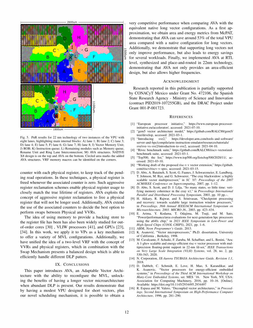
VII. SYNTHESIS AND PLACE-AND-ROUTE
Finally, we also perform experiments with design automa-tion tools to get accurate results for area and achievablefrequency. Towards this goal, we added the required AVAsupport to an in-house VPU. We present synthesis and place-and-route results for AVA and NATIVE X8 configurations.To provide the 4R-2W VRF, we implemented the LVT tech-nique [26] which provides multi-ported memories at the costof replicating and banking dual-port memories.
We obtain the main physical metrics using Cadence tools,Genus for synthesis and Innovus for place-and-route. Weselected the GLOBALFOUNDRIES 22FDX 8T technologylibraries, and we implemented the VRF slices using the Syn-opsys High-Performance Dual-Port SRAM cell-based RegisterFile Memory Compiler (R2PH). The target frequency was1GHz.
TABLE VPOST-PLACE-AND-ROUTE RESULTS.
WNS (ns) Power (mW) Area (mm2) DensityNATIVE X8 -0.244 2290 3.90 61.0%-VRF macros 388 1.252
AVA +0.119 1732 1.98 61.8%-AVA strctures 5.266 0.0042-VRF macros 184 0.257
Post-place-and-route results for the typical corner (TT 0.8V25Cº) are summarized in Table 5, and the obtained layoutsare shown in Figure 5, for both configurations. Regarding arearesults, for the AVA configuration, the required AVA hardwarestructures incur a negligible 0.21% area overhead. On the otherhand, the total chip area is reduced by 50.7% compared withthe NATIVE X8 configuration, validating the McPAT results.
Regarding the timing performance, target constraints aremet only for AVA with a positive slack of 0.119ns. However,for NATIVE X8 there is a negative slack of -0.244ns, dueto the critical paths stemming from the longer wires betweenthe SRAMs and the lane logic. Based in our synthesis andplace-and-route experiments, we can confirm that the smallsize required for AVA helps to achieve higher working fre-quencies due to a higher robustness against different physicalfloorplanning options.
VIII. RELATED WORK
AVA partially leverages different computer architecturetechniques that were developed for out-of-order cores, VLIWprocessors and GPUs. While the concepts might be familiar athigh level, we adapt and substantially tailor these techniquesfor VPs to propose the novel adaptable VRF design. Next linesbriefly describe the related work.
Different alternatives to exploit efficient use of physicalregisters was widely studied. Gonzalez et al. [19], [28]proposed a dynamic register renaming approach where the keyidea is to delay the allocation of the physical registers untilwrite-back. To this end, a technique termed as Virtual-PhysicalRegisters was proposed. Virtual-Physical Registers are notrelated to any storage location; they are merely tags to keeptrack of the dependencies and are therefore not related to AVA.Although AVA proposes a two-level renaming scheme, unlikethe Virtual-Physical Registers concept, our VVRs are assignedat renaming time, while physical registers are assigned at issuetime, and combined with the RAC counters, exploiting the useof the vector registers as soon as they can be reused.
Based on the fact that a physical register can be reusedwhen it is guaranteed that the value in it can never be used byany later instruction, several studies [9], [29], [35] associated a
11
I
J
K F
G
HD
C
B
A E
I
J
K L
L
M
F
G
HD
C
B
A E
2600um
1800um1500um
1100um
Fig. 5. PnR results for 22 nm technology of two instances of the VPU witheight lanes, highlighting main internal blocks: A) lane 1; B) lane 2; C) lane 3;D) lane 4; E) lane 5; F) lane 6; G) lane 7; H) lane 8; I) Vector Memory Unit;J) ROB; K) Instruction queue; L) Remaining modules such as Memory queue,Rename Unit and Ring Lane Interconnection; M) AVA structures. NATIVEX8 design is on the top and AVA on the bottom. Circled area marks the addedAVA structures. VRF memory macros can be identified on the corners.
counter with each physical register, to keep track of the pend-ing read operations. In these techniques, a physical register isfreed whenever the associated counter is zero. Such aggressiveregister reclamation schemes enable physical register usage toclosely match the true lifetime of registers. AVA exploits theconcept of aggressive register reclamation to free a physicalregister that will not be longer used. Additionally, AVA extendthe use of the associated counters to decide the best option toperform swaps between Physical and VVRs.
The idea of using memory to provide a backing store tothe register file has been has also been widely studied for out-of-order cores [30] , VLIW processors [41], and GPUs [23],[34]. In this work, we apply it to VPs as a key mechanismto offer a variety of MVL configurations. Additionally, wehave unified the idea of a two-level VRF with the concept ofVVRs and physical registers, which in combination with theSwap Mechanism presents a balanced design which is able toefficiently handle different DLP patters.
IX. CONCLUSIONS
This paper introduces AVA, an Adaptable Vector Archi-tecture with the ability to reconfigure the MVL, unlock-ing the benefits of having a longer vector microarchitecturewhen abundant DLP is present. Our results demonstrate thatby having a modest VPU designed for short vectors, plusour novel scheduling mechanism, it is possible to obtain a
very competitive performance when comparing AVA with theequivalent native long vector configurations. As a first ap-proximation, we obtain area and energy metrics from McPAT,demonstrating that AVA can save around 53% of the total VPUarea compared with a native configuration for long vectors.Additionally, we demonstrate that supporting long vectors notonly improve performance, but also leads to energy savingsfor several workloads. Finally, we implemented AVA at RTLlevel, synthesized and place-and-routed in 22nm technology,demonstrating that AVA not only provides an area-efficientdesign, but also allows higher frequencies.
ACKNOWLEDGMENT
Research reported in this publication is partially supportedby CONACyT Mexico under Grant No. 472106, the SpanishState Research Agency - Ministry of Science and Innovation(contract PID2019-107255GB), and the DRAC Project underGrant 001-P-001723.
REFERENCES
[1] “European processor initiative,” https://www.european-processor-initiative.eu/accelerator/, accessed: 2021-07-10.
[2] “gem5 vector architecture model,” https://github.com/RALC88/gem5/tree/develop, accessed: 2021-03-1.
[3] “Introducing sve2,” https://developer.arm.com/tools-and-software/server-and-hpc/compile/arm-instruction-emulator/resources/tutorials/sve/sve-vs-sve2/introduction-to-sve2, accessed: 2021-04-10.
[4] “Rivec benchmark suite,” https://github.com/RALC88/riscv-vectorized-benchmark-suite, accessed: 2021-03-1.
[5] “Top500, the list,” https://www.top500.org/lists/top500/2020/11/, ac-cessed: 2021-03-10.
[6] “Working draft of the proposed risc-v v vector extension,” https://github.com/riscv/riscv-v-spec, accessed: 2021-03-15.
[7] D. Abts, A. Bataineh, S. Scott, G. Faanes, J. Schwarzmeier, E. Lundberg,T. Johnson, M. Bye, and G. Schwoerer, “The cray blackwidow: a highlyscalable vector multiprocessor,” in SC ’07: Proceedings of the 2007ACM/IEEE Conference on Supercomputing, 2007, pp. 1–12.
[8] D. Abts, S. Scott, and D. J. Lilja, “So many states, so little time: veri-fying memory coherence in the cray x1,” in Proceedings InternationalParallel and Distributed Processing Symposium, 2003, pp. 10 pp.–.
[9] H. Akkary, R. Rajwar, and S. Srinivasan, “Checkpoint processingand recovery: towards scalable large instruction window processors,”in Proceedings. 36th Annual IEEE/ACM International Symposium onMicroarchitecture, 2003. MICRO-36., 2003, pp. 423–434.
[10] E. Arima, Y. Kodama, T. Odajima, M. Tsuji, and M. Sato,“Power/performance/area evaluations for next-generation hpc processorsusing the a64fx chip,” in 2021 IEEE Symposium in Low-Power andHigh-Speed Chips (COOL CHIPS), 2021, pp. 1–6.
[11] ARM, Neon Programmer’s Guide, 2013.[12] K. Asanovic, “Vector microprocessors,” Ph.D. dissertation, University
of California , Berkeley, 1998.[13] M. Cavalcante, F. Schuiki, F. Zaruba, M. Schaffner, and L. Benini, “Ara:
A 1-ghz+ scalable and energy-efficient risc-v vector processor with mul-tiprecision floating-point support in 22-nm fd-soi,” IEEE Transactionson Very Large Scale Integration (VLSI) Systems, vol. 28, no. 2, pp.530–543, 2020.
[14] N. Corporation, SX-Aurora TSUBASA Architecture Guide, Revision 1.1,2018.
[15] D. Dabbelt, C. Schmidt, E. Love, H. Mao, S. Karandikar, andK. Asanovic, “Vector processors for energy-efficient embeddedsystems,” in Proceedings of the Third ACM International Workshop onMany-Core Embedded Systems, ser. MES ’16. New York, NY, USA:Association for Computing Machinery, 2016, pp. 10–16. [Online].Available: https://doi.org/10.1145/2934495.2934497
[16] R. Espasa and M. Valero, “Decoupled vector architectures,” in Proceed-ings. Second International Symposium on High-Performance ComputerArchitecture, 1996, pp. 281–290.
12

[17] M. Flynn, “Very high-speed computing systems,” Proceedings of theIEEE, vol. 54, no. 12, pp. 1901–1909, 1966.
[18] G. Gobieski, A. Nagi, N. Serafin, M. M. Isgenc, N. Beckmann, andB. Lucia, “Manic: A vector-dataflow architecture for ultra-low-powerembedded systems,” in Proceedings of the 52nd Annual IEEE/ACMInternational Symposium on Microarchitecture, ser. MICRO ’52. NewYork, NY, USA: Association for Computing Machinery, 2019, pp.670–684. [Online]. Available: https://doi.org/10.1145/3352460.3358277
[19] A. Gonzalez, J. Gonzalez, and M. Valero, “Virtual-physical registers,” inProceedings of the 4th International Symposium on High-PerformanceComputer Architecture, ser. HPCA ’98. USA: IEEE Computer Society,1998, p. 175.
[20] J. L. Hennessy and D. A. Patterson, Computer architecture : a quanti-tative approach. Morgan Kaufmann Publishers, 2019.
[21] C. R. Inc, The CRAY-2 computer system, 1985.[22] Intel, Instruction Set Extensions and Future Features Programming
Reference, 2020.[23] J. Kloosterman, J. Beaumont, D. A. Jamshidi, J. Bailey, T. Mudge,
and S. Mahlke, “Regless: Just-in-time operand staging for gpus,” inProceedings of the 50th Annual IEEE/ACM International Symposiumon Microarchitecture, ser. MICRO-50 ’17. New York, NY, USA:Association for Computing Machinery, 2017, p. 151–164. [Online].Available: https://doi.org/10.1145/3123939.3123974
[24] C. E. Kozyrakis and D. A. Patterson, “Scalable, vector processors forembedded systems,” IEEE Micro, vol. 23, no. 6, pp. 36–45, 2003.
[25] R. Krashinsky, C. Batten, M. Hampton, S. Gerding, B. Pharris, J. Casper,and K. Asanovic, “The vector-thread architecture,” in Proceedings of the31st Annual International Symposium on Computer Architecture, ser.ISCA ’04. USA: IEEE Computer Society, 2004, p. 52.
[26] C. E. LaForest and J. G. Steffan, “Efficient multi-ported memories forfpgas,” in Proceedings of the 18th Annual ACM/SIGDA InternationalSymposium on Field Programmable Gate Arrays, ser. FPGA ’10.New York, NY, USA: Association for Computing Machinery, 2010, p.41–50. [Online]. Available: https://doi.org/10.1145/1723112.1723122
[27] MIPS, MIPS Architecture for Programmers : The MIPS64 SIMD Archi-tecture Module, 2016.
[28] T. Monreal, A. Gonzalez, M. Valero, J. Gonzalez, and V. Vinals,“Delaying physical register allocation through virtual-physical registers,”in MICRO-32. Proceedings of the 32nd Annual ACM/IEEE InternationalSymposium on Microarchitecture, 1999, pp. 186–192.
[29] M. Moudgill, K. Pingali, and S. Vassiliadis, “Register renaming anddynamic speculation: An alternative approach,” in Proceedings of the26th Annual International Symposium on Microarchitecture, ser. MICRO26. Washington, DC, USA: IEEE Computer Society Press, 1993, p.202–213.
[30] D. Oehmke, N. Binkert, T. Mudge, and S. Reinhardt, “How to fake1000 registers,” in 38th Annual IEEE/ACM International Symposium onMicroarchitecture (MICRO’05), 2005, pp. 12 pp.–18.
[31] C. Ramırez, C. A. Hernandez, O. Palomar, O. Unsal, M. A.Ramırez, and A. Cristal, “A risc-v simulator and benchmark suitefor designing and evaluating vector architectures,” ACM Trans.Archit. Code Optim., vol. 17, no. 4, Nov. 2020. [Online]. Available:https://doi.org/10.1145/3422667
[32] S. Rivoire, R. Schultz, T. Okuda, and C. Kozyrakis, “Vector lanethreading,” in 2006 International Conference on Parallel Processing(ICPP’06), 2006, pp. 55–64.
[33] R. M. Russell, “The cray-1 computer system,” Commun. ACM,vol. 21, no. 1, pp. 63–72, Jan. 1978. [Online]. Available: https://doi.org/10.1145/359327.359336
[34] M. Sadrosadati, A. Mirhosseini, A. Hajiabadi, S. B. Ehsani, H. Falahati,H. Sarbazi-Azad, M. Drumond, B. Falsafi, R. Ausavarungnirun, andO. Mutlu, “Highly concurrent latency-tolerant register files for gpus,”ACM Trans. Comput. Syst., vol. 37, no. 1–4, Jan. 2021. [Online].Available: https://doi.org/10.1145/3419973
[35] J. Smith and G. Sohi, “The microarchitecture of superscalar processors,”Proceedings of the IEEE, vol. 83, no. 12, pp. 1609–1624, 1995.
[36] N. Stephens, S. Biles, M. Boettcher, J. Eapen, M. Eyole, G. Gabrielli,M. Horsnell, G. Magklis, A. Martinez, N. Premillieu, A. Reid, A. Rico,and P. Walker, “The arm scalable vector extension,” IEEE Micro, vol. 37,no. 2, pp. 26–39, 2017.
[37] N. Stephens, S. Biles, M. Boettcher, J. Eapen, M. Eyole, G. Gabrielli,M. Horsnell, G. Magklis, A. Martinez, N. Premillieu, A. Reid, A. Rico,and P. Walker, “The arm scalable vector extension,” IEEE Micro, vol. 37,no. 2, pp. 26–39, 2017.
[38] C. C. systems, CRAY-2 Computer System Functional Description, 1985.[39] Y. Yamada, “Vector engine processor of nec's brand-new supercomputer
sx-aurora tsubasa,” in NEC Corporation, 2018.[40] T. Yoshida, “Introduction of fujitsu's hpc processor for the post-k,” in
Hot Chips, 2016.[41] J. Zalamea, J. Llosa, E. Ayguade, and M. Valero, “Two-level hierar-
chical register file organization for vliw processors,” in Proceedings33rd Annual IEEE/ACM International Symposium on Microarchitecture.MICRO-33 2000, 2000, pp. 137–146.
[42] V. Zyuban and P. Kogge, “The energy complexity of register files,”in Proceedings of the 1998 International Symposium on Low PowerElectronics and Design, ser. ISLPED ’98. New York, NY, USA:Association for Computing Machinery, 1998, p. 305–310. [Online].Available: https://doi.org/10.1145/280756.280943
13