ad9059
DESCRIPTION
a/d converterTRANSCRIPT

REV. A
Information furnished by Analog Devices is believed to be accurate andreliable. However, no responsibility is assumed by Analog Devices for itsuse, nor for any infringements of patents or other rights of third parties thatmay result from its use. No license is granted by implication or otherwiseunder any patent or patent rights of Analog Devices. Trademarks andregistered trademarks are the property of their respective companies.
One Technology Way, P.O. Box 9106, Norwood, MA 02062-9106, U.S.A.
Tel: 781/329-4700 www.analog.com
Fax: 781/326-8703 © 2003 Analog Devices, Inc. All rights reserved.
AD9059Dual 8-Bit, 60 MSPS A/D Converter
FEATURES
Dual 8-Bit ADCs on a Single Chip
Low Power: 400 mW Typical
On-Chip 2.5 V Reference and Track-and-Hold
1 V p-p Analog Input Range
Single 5 V Supply Operation
5 V or 3 V Logic Interface
120 MHz Analog Bandwidth
Power-Down Mode: <12 mW
APPLICATIONS
Digital Communications (QAM Demodulators)
RGB and YC/Composite Video Processing
Digital Data Storage Read Channels
Medical Imaging
Digital Instrumentation
FUNCTIONAL BLOCK DIAGRAM
ADCAT/H
ADCB
2.5V
T/H
8
8
ENCODE
AINA
AINB
VREF
VD
GND
PWRDN
AD9059
VDD
D7A–D0A
D7B–D0B
PRODUCT DESCRIPTIONThe AD9059 is a dual 8-bit monolithic analog-to-digital converteroptimized for low cost, low power, small size, and ease of use.With a 60 MSPS encode rate capability and full-power analogbandwidth of 120 MHz typical, the component is ideal forapplications requiring multiple ADCs with excellent dynamicperformance.
To minimize system cost and power dissipation, the AD9059includes an internal 2.5 V reference and dual track-and-holdcircuits. The ADC requires only a 5 V power supply and anencode clock. No external reference or driver components arerequired for many applications.
The AD9059’s single encode input is TTL/CMOS compatibleand simultaneously controls both internal ADC channels. Theparallel 8-bit digital outputs can be operated from 5 V or 3 Vsupplies. A power-down function may be exercised to bringtotal consumption to <12 mW when ADC data is not requiredfor lengthy periods of time. In power-down mode, the digitaloutputs are driven to a high impedance state.
Fabricated on an advanced BiCMOS process, the AD9059is available in a space-saving 28-lead shrink small outlinepackage (28-lead SSOP) and is specified over the industrialtemperature range (–40°C to +85°C).
Customers desiring single-channel digitization may consider theAD9057, a single 8-bit, 60 MSPS monolithic based on theAD9059 ADC core. The AD9057 is available in a 20-lead shrinksmall outline package (20-lead SSOP) and is specified over theindustrial temperature range.
PIN CONFIGURATION
14
13
12
11
10
17
16
15
19
18
20
28
27
26
25
24
23
22
21
9
8
1
2
3
4
7
6
5
TOP VIEW(Not to Scale)
AD9059
AINA
VD
ENCODE
GND
AINB
VREF
PWRDN
VD
D7B (MSB)
VDD
GNDGND
VDD
D7A (MSB)
D6A
D5A
D4A D4B
D5B
D6B
D3A
D2A
D1A
D0A (LSB)
D3B
D0B (LSB)
D1B
D2B

REV. A–2–
AD9059–SPECIFICATIONSELECTRICAL CHARACTERISTICS (VD = 5 V, VDD = 3 V, external reference, ENCODE = 60 MSPS, unless otherwise noted.)
AD9059BRSParameter Temp Test Level Min Typ Max Unit
RESOLUTION 8 Bits
DC ACCURACYDifferential Nonlinearity 25°C I 0.75 2.0 LSB
Full VI 2.5 LSBIntegral Nonlinearity 25°C I 0.75 2.0 LSB
Full VI 2.5 LSBNo Missing Codes Full VI GuaranteedGain Error1 25°C I –6 –2.5 +6 % FS
Full VI –8 +8 % FSGain Temperature Coefficient1 Full V ±70 ppm/°C
ANALOG INPUTInput Voltage Range (Centered at 2.5 V) 25°C V 1.0 V p-pInput Offset Voltage 25°C I –15 0 +15 mV
Full VI –25 +25 mVInput Resistance 25°C V 150 kΩInput Capacitance 25°C V 2 pFInput Bias Current 25°C I 6 16 µAAnalog Bandwidth 25°C V 120 MHz
CHANNEL MATCHING (A to B)Gain Delta 25°C V ±1 % FSInput Offset Voltage Delta 25°C V ±4 mV
BAND GAP REFERENCEOutput Voltage Full VI 2.4 2.5 2.6 VTemperature Coefficient Full V ±10 ppm/°C
SWITCHING PERFORMANCEMaximum Conversion Rate Full VI 60 MSPSMinimum Conversion Rate Full IV 5 MSPSAperture Delay (tA) 25°C V 2.7 nsAperture Uncertainty (Jitter) 25°C V 5 ps, rmsOutput Valid Time (tV)2 Full IV 4.0 6.6 nsOutput Propagation Delay (tPD)2 Full IV 9.5 14.2 ns
DYNAMIC PERFORMANCE3
Transient Response 25°C V 9 nsOvervoltage Recovery Time 25°C V 9 nsSignal-to-Noise Ratio (SINAD) (with Harmonics)
fIN = 10.3 MHz 25°C I 40 44.5 dBfIN = 76 MHz 25°C V 43.5 dB
Effective Number of Bits (ENOB)fIN = 10.3 MHz 25°C I 6.35 7.1 BitsfIN = 76 MHz 25°C V 6.9 Bits
Signal-to-Noise Ratio (SNR) (Without Harmonics)fIN = 10.3 MHz 25°C I 42 46 dBfIN = 76 MHz 25°C V 45 dB
Second Harmonic DistortionfIN = 10.3 MHz 25°C I –50 –62 dBcfIN = 76 MHz 25°C V –54 dBc
Third Harmonic DistortionfIN = 10.3 MHz 25°C I –46 –60 dBcfIN = 76 MHz 25°C V –54 dBc
Two-Tone Intermodulation Distortion (IMD) 25°C V –52 dBcChannel Crosstalk Rejection 25°C V –50 dBcDifferential Phase 25°C V 0.8 DegreesDifferential Gain 25°C V 1.0 %

REV. A
AD9059
–3–
SPECIFICATIONS (continued)
AD9059BRSParameter Temp Test Level Min Typ Max Unit
DIGITAL INPUTSLogic 1 Voltage Full VI 2.0 VLogic 0 Voltage Full VI 0.8 VLogic 1 Current Full VI ±1 µALogic 0 Current Full VI ±1 µAInput Capacitance 25°C V 4.5 pFEncode Pulsewidth High (tEH) 25°C IV 6.7 166 nsEncode Pulsewidth Low (tEL) 25°C IV 6.7 166 ns
DIGITAL OUTPUTSLogic 1 Voltage (VDD = 3 V) Full VI 2.95 VLogic 1 Voltage (VDD = 5 V) Full IV 4.95 VLogic 0 Voltage (VDD = 3 V or 5 V) Full VI 0.05 VOutput Coding Offset Binary Code
POWER SUPPLYVD Supply Current (VD = 5 V) Full VI 72 92 mAVDD Supply Current (VDD = 3 V)4 Full VI 13 15 mAPower Dissipation5, 6 Full VI 400 505 mWPower-Down Dissipation Full VI 6 12 mWPower Supply Rejection Ratio (PSRR) 25°C I 3 mV/V
NOTES1Gain error and gain temperature coefficient are based on the ADC only (with a fixed 2.5 V external reference).2tV and tPD are measured from the 1.5 V level of the ENCODE to the 10%/90% levels of the digital output swing. The digital output load during test is not to exceedan ac load of 10 pF or a dc current of ± 40 µA.
3SNR/harmonics based on an analog input voltage of –0.5 dBFS referenced to a 1.0 V full-scale input range.4Digital supply current based on VDD = 3 V output drive with <10 pF loading under dynamic test conditions.5Power dissipation is based on 60 MSPS encode and 10.3 MHz analog input dynamic test conditions (VD = 5 V ± 5%, VDD = 3 V ± 5%).6Typical thermal impedance for the RS style (SSOP) 28-lead package: θJC = 39°C/W, θCA = 70°C/W, and θJA = 109°C/W.
Specifications subject to change without notice.
EXPLANATION OF TEST LEVELSTest LevelI – 100% production tested.
II – 100% production tested at +25°C and sample tested atspecified temperatures.
III – Sample tested only.
IV – Parameter is guaranteed by design and characterizationtesting.
V – Parameter is a typical value only.
VI – 100% production tested at +25°C; guaranteed by designand characterization testing for industrial temperature range.
ABSOLUTE MAXIMUM RATINGS*
VD, VDD . . . . . . . . . . . . . . . . . . . . . . . . . . . . . . . . . . . . . . . . 7 VAnalog Inputs . . . . . . . . . . . . . . . . . . . . . . . –0.5 V to VD + 0.5 VDigital Inputs . . . . . . . . . . . . . . . . . . . . . . . –0.5 V to VD + 0.5 VVREF Input . . . . . . . . . . . . . . . . . . . . . . . . . –0.5 V to VD + 0.5 VDigital Output Current . . . . . . . . . . . . . . . . . . . . . . . . . . . 20 mAOperating Temperature . . . . . . . . . . . . . . . . . . –55°C to +125°CStorage Temperature . . . . . . . . . . . . . . . . . . . . –65°C to +150°C
*Stresses above those listed under Absolute Maximum Ratings may cause permanentdamage to the device. This is a stress rating only; functional operation of the deviceat these or any other conditions above those indicated in the operational sections ofthis specification is not implied. Exposure to absolute maximum ratings for extendedperiods may affect device reliability.
ORDERING GUIDE
Model Temperature Range Package Option
AD9059BRS –40°C to +85°C RS-28AD9059/PCB 25°C Evaluation Board
CAUTIONESD (electrostatic discharge) sensitive device. Electrostatic charges as high as 4000 V readilyaccumulate on the human body and test equipment and can discharge without detection. Although theAD9059 features proprietary ESD protection circuitry, permanent damage may occur on devicessubjected to high energy electrostatic discharges. Therefore, proper ESD precautions are recommendedto avoid performance degradation or loss of functionality.

REV. A–4–
AD9059
N N + 3 N + 5
N + 1
N + 2N + 4
tA
tV
tPD
tEH tEL
N – 3 N – 2 N – 1 N N + 1 N + 2
ENCODE
AIN
DIGITALOUTPUTS
APERTURE DELAY
PULSEWIDTH HIGH
PULSEWIDTH LOW
OUTPUT VALID TIME
OUTPUT PROP DELAY
6.7ns
6.7ns
4.0ns
166ns
166ns
14.2ns
MIN TYP MAX
9.5ns
6.6n
2.7nstA
tEH
tEL
tV
tPD
Figure 1. Timing Diagram
PIN CONFIGURATION
14
13
12
11
10
17
16
15
19
18
20
28
27
26
25
24
23
22
21
9
8
1
2
3
4
7
6
5
TOP VIEW(Not to Scale)
AD9059
AINA
VD
ENCODE
GND
AINB
VREF
PWRDN
VD
D7B (MSB)
VDD
GNDGND
VDD
D7A (MSB)
D6A
D5A
D4A D4B
D5B
D6B
D3A
D2A
D1A
D0A (LSB)
D3B
D0B (LSB)
D1B
D2B
PIN FUNCTION DESCRIPTIONS
Pin No. Mnemonic Function
1, 28 AINA, AINB Analog Inputs for ADC A and B.
2 VREF Internal Voltage Reference (2.5 VTypical); Bypass with 0.1 µF toGround or Overdrive with ExternalVoltage Reference.
3 PWRDN Power-Down Function Select; LogicHIGH for Power-Down Mode(Digital Outputs Go to High-Impedance State).
4, 25 VD Analog 5 V Power Supply.
5, 24, 27 GND Ground.
6, 23 VDD Digital Output Power Supply.Nominally 3 V to 5 V.
7–14 D7A–D0A Digital Outputs of ADC A.
22–15 D7B–D0B Digital Outputs of ADC B.
26 ENCODE Encode Clock for ADCs A and B(ADCs Sample Simultaneously onthe Rising Edge of ENCODE).
Table I. Digital Coding (VREF = 2.5 V)
Analog Input (V) Voltage Level Digital Output
3.0 Positive Full Scale 1111 11112.502 Midscale + 1/2 LSB 1000 00002.498 Midscale – 1/2 LSB 0111 11112.0 Negative Full Scale 0000 0000

REV. A
Typical Performance Characteristics–AD9059
–5–
FREQUENCY (MHz)
0
–30
–90
–60
–20
–10
–80
–70
–50
–40
0 30
ENCODE = 60MSPS ANALOG IN = 10.3MHz, –0.5dBFS SINAD = 43.9dB ENOB = 7.0 BITS SNR = 45.1dB
dB
TPC 1. FFT Spectral Plot 60 MSPS, 10.3 MHz
FREQUENCY (MHz)
0
–30
–90
–60
–20
–10
–50
–40
–80
–70
0 30
ENCODE = 60MSPS ANALOG IN = 76MHz, –0.5dBFS SINAD = 43.0dB ENOB = 6.85 BITS SNR = 44.1dB
dB
TPC 2. Spectral Plot 60 MSPS, 76 MHz
ANALOG INPUT FREQUENCY (MHz)
dB
0 16020 40 60 80 100 120 140
46
30
38
36
34
32
42
40
44
ENCODE = 60MSPS AIN = –0.5dBFS
SNR
SINAD
TPC 3. SINAD/SNR vs. AIN Frequency
ANALOG INPUT FREQUENCY (MHz)
–30
–700 16020 40 60 80 100 120 140
–35
–50
–55
–60
–65
–40
–45
SECOND HARMONIC
THIRD HARMONIC
ENCODE = 60MSPS AIN = –0.5dBFS
dB
TPC 4. Harmonic Distortion vs. AIN Frequency
FREQUENCY (MHz)
dB
0
–10
–900 3010 20
–50
–60
–70
–80
–30
–40
–20
ENCODE = 60MSPSF1 IN = 9.5MHz @ –7.0dBFSF2 IN = 9.9MHz @ –7.0dBFS2F1 - F2 = –52.0dBc2F2 - F1 = –53.0dBc
TPC 5. Two-Tone IMD
ENCODE RATE (MSPS)
dB
54
24
65 10 20 30 40 50 60 70 80 90
48
30
18
12
42
36
AIN = 10.3MHz, –0.5dBFS SNR
SINAD
TPC 6. SINAD/SNR vs. Encode Rate
REV. A–6–
AD9059
ENCODE RATE (MSPS)
PO
WE
R (
mW
)
600
400
2505 10 20 30 40 50 60 70 80 90
550
500
350
300
450
AIN = 10.3MHz, –0.5dBFS
VDD = 5V
VDD = 3V
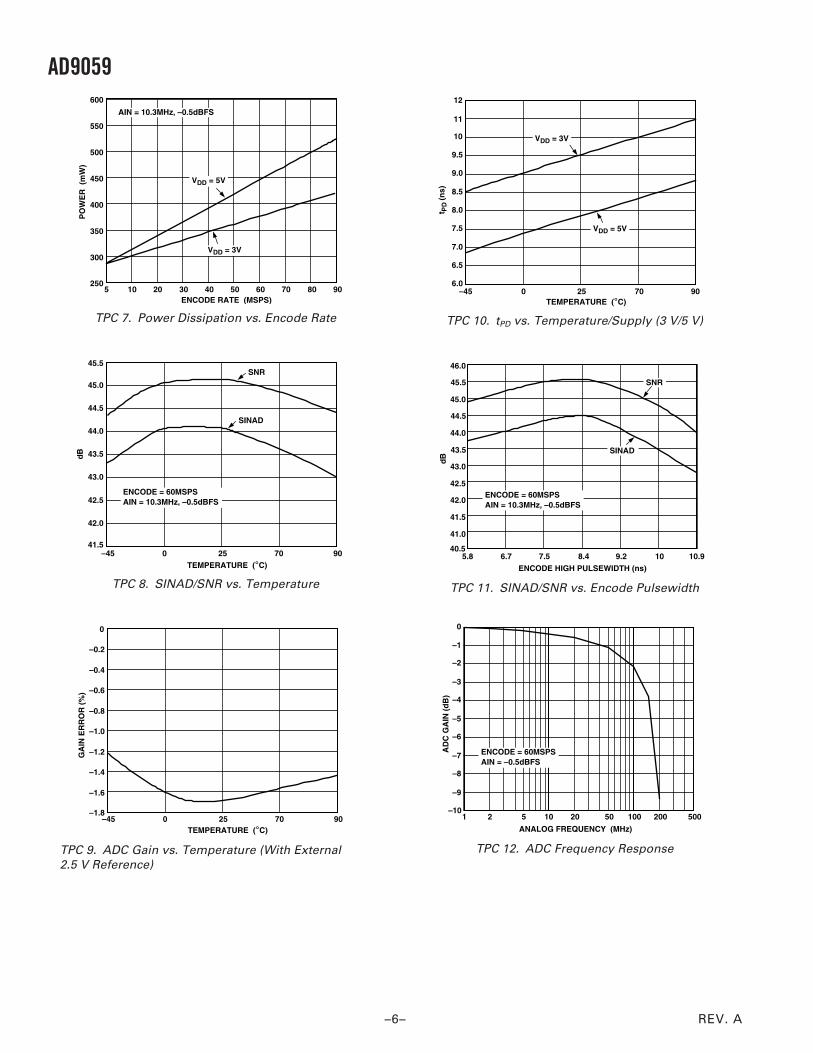
TPC 7. Power Dissipation vs. Encode Rate
TEMPERATURE (°C)
45.5
dB
45.0
41.5–45 900 25 70
43.5
43.0
42.5
42.0
44.5
44.0
SNR
SINAD
ENCODE = 60MSPS AIN = 10.3MHz, –0.5dBFS
TPC 8. SINAD/SNR vs. Temperature
TEMPERATURE (°C)
0
GA
IN E
RR
OR
(%
)
–0.2
–1.8–45 900 25 70
–0.8
–1.2
–1.4
–1.6
–0.4
–0.6
–1.0
TPC 9. ADC Gain vs. Temperature (With External2.5 V Reference)
TEMPERATURE (°C)
10
t PD
(ns)
9.5
–45 900 25 70
8.0
6.5
6.0
9.0
8.5
7.0
7.5 VDD = 5V
VDD = 3V
11
12
TPC 10. tPD vs. Temperature/Supply (3 V/5 V)
dB
ENCODE HIGH PULSEWIDTH (ns)
46.0
45.5
40.55.8 10.9
44.5
44.0
43.5
43.0
45.0
41.0
41.5
42.0
42.5
6.7 7.5 8.4 9.2 10
SNR
ENCODE = 60MSPS AIN = 10.3MHz, –0.5dBFS
SINAD
TPC 11. SINAD/SNR vs. Encode Pulsewidth
ANALOG FREQUENCY (MHz)
AD
C G
AIN
(d
B)
0
–2
1 50010 100
–4
–6
–8
–10
ENCODE = 60MSPS AIN = –0.5dBFS
–1
–3
–5
–9
–7
2 5 20 50 200
TPC 12. ADC Frequency Response

REV. A
AD9059
–7–
THEORY OF OPERATIONThe AD9059 combines Analog Devices’ proprietary MagAmpgray code conversion circuitry with flash converter technology toprovide dual high performance 8-bit ADCs in a single low costmonolithic device. The design architecture ensures low power,high speed, and 8-bit accuracy.
The AD9059 provides two linked ADC channels that are clockedfrom a single ENCODE input (see Functional Block Diagram).The two ADC channels simultaneously sample the analog inputs(AINA and AINB) and provide noninterleaved parallel digitaloutputs (D0A–D7A and D0B–D7B). The voltage reference(VREF) is internally connected to both ADCs so channel gainsand offsets will track if external reference control is desired.
The analog input signal is buffered at the input of each ADCchannel and applied to a high speed track-and-hold. The track-and-hold circuit holds the analog input value during theconversion process (beginning with the rising edge of theENCODE command). The track-and-hold’s output signal passesthrough the gray code and flash conversion stages to generatecoarse and fine digital representations of the held analog inputlevel. Decode logic combines the multistage data and aligns the8-bit word for strobed outputs on the rising edge of the ENCODEcommand. The MagAmp/Flash architecture of the AD9059results in three pipeline delays for the output data.
USING THE AD9059Analog InputsThe AD9059 provides independent single-ended high impedance(150 kΩ) analog inputs for the dual ADCs. Each input requires adc bias current of 6 µA (typical) centered near 2.5 V (±10%). Thedc bias may be provided by the user or may be derived from theADC’s internal voltage reference. Figure 2 shows a low cost dcbias implementation that allows the user to capacitively coupleac signals directly into the ADC without additional active cir-cuitry. For best dynamic performance, the VREF pin shouldbe decoupled to ground with a 0.1 µF capacitor (to minimizemodulation of the reference voltage), and the bias resistor shouldbe approximately 1 kΩ.
1
3
1k
1k
AINA
AINB
VREF
AD9059
0.1µF
0.1µF
0.1µF
5V
VINA(1V p-p)
EXTERNAL VREF(OPTIONAL)
VINB(1V p-p)
28
Figure 2. Capacity Coupled AD9059
Figure 3 shows typical connections for high performance dcbiasing using the ADC’s internal voltage reference. All compo-nents may be powered from a single 5 V supply (analog inputsignals are referenced to ground).
28
1
10k
1k
AINA
AINB
VREF
AD90590.1µF
+5V
VINA
VINB(–0.5V TO +0.5V)
10k
+5V
5V
AD8041
AD8041
1k
1k
1k
3
Figure 3. DC-Coupled AD9059 (VIN Inverted)
Voltage ReferenceA stable and accurate 2.5 V voltage reference is built into theAD9059 (VREF). The reference output is used to set the ADCgain/offset and can provide dc bias for the analog input signals.The internal reference is tied to the ADC circuitry through an800 Ω internal impedance and is capable of providing 300 µAexternal drive current (for dc biasing the analog input or otheruser circuitry).
Some applications may require greater accuracy, improvedtemperature performance, or gain adjustments that cannot beobtained using the internal reference. An external voltage maybe applied to the VREF pin to overdrive the internal voltagereference for gain adjustment of up to ±10% (the VREF pin isinternally tied directly to the ADC circuitry). ADC gain andoffset will vary simultaneously with external reference adjust-ment with a 1:1 ratio (a 2% or 50 mV adjustment to the 2.5 Vreference varies ADC gain by 2% and ADC offset by 50 mV).
Theoretical input voltage range versus reference input voltagemay be calculated using the following equations.
V p p VREF
V VREF
V VREF V
V VREF V
RANGE
MIDSCALE
TOP OF RANGE RANGE
BOTTOM OF RANGE RANGE
( ) .
–
− ==
= +=
− −
− −
2 5
2
2
The external reference should have a 1 mA minimum sink/source current capability to ensure complete overdrive of theinternal voltage reference.

REV. A–8–
AD9059Digital Logic (5 V/3 V Systems)The digital inputs and outputs of the AD9059 can easily beconfigured to interface directly with 3 V or 5 V logic systems.The encode and power-down (PWRDN) inputs are CMOSstages with TTL thresholds of 1.5 V, making the inputs compat-ible with TTL, 5 V CMOS, and 3 V CMOS logic families. Aswith all high speed data converters, the encode signal should beclean and jitter free to prevent degradation of ADC dynamicperformance.
The AD9059’s digital outputs will also interface directly with 5 Vor 3 V CMOS logic systems. The voltage supply pins (VDD) forthese CMOS stages are isolated from the analog VD voltagesupply. By varying the voltage on these supply pins, the digitaloutput high levels will change for 5 V or 3 V systems. The VDD
pins are internally connected on the AD9059 die. Care shouldbe taken to isolate the VDD supply voltages from the 5 V analogsupply to minimize noise coupling into the ADCs.
The AD9059 provides high impedance digital output operationwhen the ADC is driven into power-down mode (PWRDN,logic high). A 200 ns (minimum) power-down time should beprovided before a high impedance characteristic is required. A200 ns power-up period should be provided to ensure accurateADC output data after reactivation (valid output data is avail-able three clock cycles after the 200 ns delay).
TimingThe AD9059 is guaranteed to operate with conversion ratesfrom 5 MSPS to 60 MSPS. At 60 MSPS, the ADC is designedto operate with an encode duty cycle of 50%, but performanceis insensitive to moderate variations. Pulsewidth variations of upto ±10% (allowing the encode signal to meet the minimum/maximum high/low specifications) will cause no degradation inADC performance (see Figure 1).
Due to the linked ENCODE architecture of the ADCs, theAD9059 cannot be operated in a 2-channel ping-pong mode.
Power DissipationThe power dissipation of the AD9059 is specified to reflect atypical application setup under the following conditions: encodeis 60 MSPS, analog input is –0.5 dBFS at 10.3 MHz, VD is 5 V,VDD is 3 V, and digital outputs are loaded with 7 pF typical(10 pF maximum). The actual dissipation will vary as theseconditions are modified in user applications. TPC 7 shows typi-cal power consumption for the AD9059 versus ADC encodefrequency and VDD supply voltage.
A power-down function allows users to reduce power dissipationwhen ADC data is not required. A TTL/CMOS high signal(PWRDN) shuts down portions of the dual ADC and brings totalpower dissipation to less than 10 mW. The internal band gapvoltage reference remains active during power-down mode tominimize ADC reactivation time. If the power-down function isnot desired, Pin 3 should be tied to ground. Both ADC channelsare controlled simultaneously by the PWRDN pin; they cannotbe shut down or turned on independently.
ApplicationsThe wide analog bandwidth of the AD9059 makes it attractive fora variety of high performance receiver and encoder applications.Figure 4 shows the dual ADC in a typical low cost I and Qdemodulator implementation for cable, satellite, or wirelessLAN modem receivers. The excellent dynamic performance ofthe ADC at higher analog input frequencies and encode ratesempowers users to employ direct IF sampling techniques (seeTPC 2). IF sampling eliminates or simplifies analog mixer andfilter stages to reduce total system cost and power.
AD9059
BPF
BPF
90°
VCO
IF IN
VCO
ADC
ADC
Figure 4. I and Q Digital Receiver
The high sampling rate and analog bandwidth of the AD9059are ideal for computer RGB video digitizer applications. With afull-power analog bandwidth of 2× the maximum sampling rate,the ADC provides sufficient pixel-to-pixel transient settling timeto ensure accurate 60 MSPS video digitization. Figure 5 showsa typical RGB video digitizer implementation for the AD9059.
8RED
GREEN
AD9059
BLUE
AD9059
H-SYNC PLLPIXEL CLOCK
8
8
ADC
ADC
ADC
ADC
Figure 5. RGB Video Encoder
REV. A
AD9059
–9–
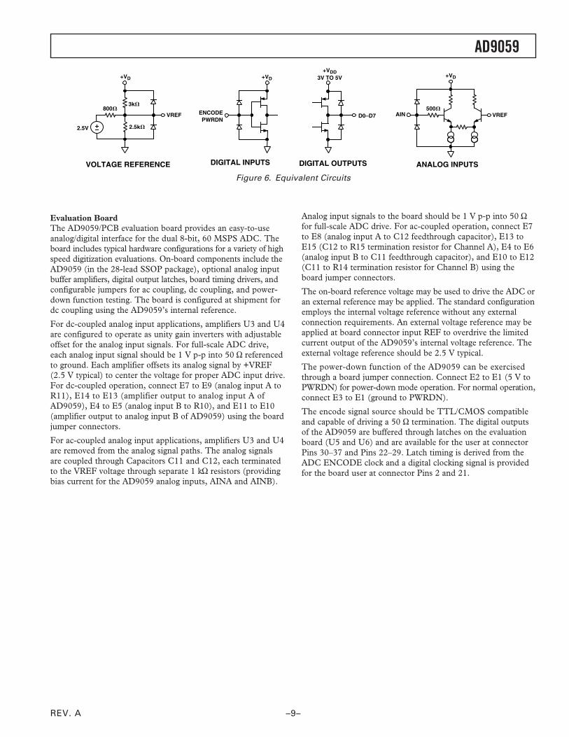
Evaluation BoardThe AD9059/PCB evaluation board provides an easy-to-useanalog/digital interface for the dual 8-bit, 60 MSPS ADC. Theboard includes typical hardware configurations for a variety of highspeed digitization evaluations. On-board components include theAD9059 (in the 28-lead SSOP package), optional analog inputbuffer amplifiers, digital output latches, board timing drivers, andconfigurable jumpers for ac coupling, dc coupling, and power-down function testing. The board is configured at shipment fordc coupling using the AD9059’s internal reference.
For dc-coupled analog input applications, amplifiers U3 and U4are configured to operate as unity gain inverters with adjustableoffset for the analog input signals. For full-scale ADC drive,each analog input signal should be 1 V p-p into 50 Ω referencedto ground. Each amplifier offsets its analog signal by +VREF(2.5 V typical) to center the voltage for proper ADC input drive.For dc-coupled operation, connect E7 to E9 (analog input A toR11), E14 to E13 (amplifier output to analog input A ofAD9059), E4 to E5 (analog input B to R10), and E11 to E10(amplifier output to analog input B of AD9059) using the boardjumper connectors.
For ac-coupled analog input applications, amplifiers U3 and U4are removed from the analog signal paths. The analog signalsare coupled through Capacitors C11 and C12, each terminatedto the VREF voltage through separate 1 kΩ resistors (providingbias current for the AD9059 analog inputs, AINA and AINB).
Analog input signals to the board should be 1 V p-p into 50 Ωfor full-scale ADC drive. For ac-coupled operation, connect E7to E8 (analog input A to C12 feedthrough capacitor), E13 toE15 (C12 to R15 termination resistor for Channel A), E4 to E6(analog input B to C11 feedthrough capacitor), and E10 to E12(C11 to R14 termination resistor for Channel B) using theboard jumper connectors.
The on-board reference voltage may be used to drive the ADC oran external reference may be applied. The standard configurationemploys the internal voltage reference without any externalconnection requirements. An external voltage reference may beapplied at board connector input REF to overdrive the limitedcurrent output of the AD9059’s internal voltage reference. Theexternal voltage reference should be 2.5 V typical.
The power-down function of the AD9059 can be exercisedthrough a board jumper connection. Connect E2 to E1 (5 V toPWRDN) for power-down mode operation. For normal operation,connect E3 to E1 (ground to PWRDN).
The encode signal source should be TTL/CMOS compatibleand capable of driving a 50 Ω termination. The digital outputsof the AD9059 are buffered through latches on the evaluationboard (U5 and U6) and are available for the user at connectorPins 30–37 and Pins 22–29. Latch timing is derived from theADC ENCODE clock and a digital clocking signal is providedfor the board user at connector Pins 2 and 21.
+VD
ENCODEPWRDN
D0–D7
+VDD3V TO 5V
500
+VD
VREFAIN
DIGITAL INPUTS ANALOG INPUTSDIGITAL OUTPUTS
800
+VD
VREF
3k
2.5k2.5V
VOLTAGE REFERENCE
Figure 6. Equivalent Circuits

REV. A–10–
AD9059
12
131415
1617
1819
98
76
543
2
CK OE111
U574ACQ574
8D
7D6D5D
4D3D2D
1D
8Q7Q6Q
5Q4Q3Q2Q
1Q
D0B
D1BD2B
D3BD4BD5B
D6BD7B
DB0
DB1DB2
DB3DB4DB5
DB6DB7
12
1314
151617
1819
9
876
54
32
CK OE111
U674ACQ574
8D7D6D
5D4D3D
2D1D
8Q7Q
6Q5Q4Q3Q
2Q1Q
D7AD6A
D5AD4AD3A
D2AD1A
D0A
DA7DA6DA5
DA4DA3
DA2DA1DA0
1
23
4
56
U774AC00
12
1311
R1550
12
345
678
91011
1213
14
2827
262524
2322
212019
181716
15
5V 5V
E10
E3
E11
C120.1µF
E14
E15E13
PWRDN
5V E1E2
E12
R510
R141k
8
765
DIS+VS
NC
NC
–VS
U4AD8041Q
123
4R111k
E8
R1350
BNCJ5
ANALOG IN–A
123456
789
10111213
1415161718
192021
22232425262728
2930313233343536
37
P2C37DRPF
R71k
BNCJ10
ENCODE
J12, GND
C140.1µF
C70.1µF
C60.1µF
C1510µF
C130.1µF
C50.1µF
C40.1µF
C30.1µF
5V
DECOUPLING CAPS
J11, VD
E7
E9
U1AD9059RS
AINA
VREFPWRDN
GND
VD
VDDD7AD6AD5AD4A
D3AD2AD1A
D0A
AINB
GNDENC
GND
VD
VDD
D7BD6BD5BD4B
D3BD2BD1B
D0B
D7BD6BD5BD4B
D3BD2BD1B
D0B
C80.1µF
C1610µF
J9, VDD
C90.1µF
DB0DB1DB2
DB3DB4DB5DB6DB7DA0DA1DA2DA3
DA4DA5DA6DA7
U774AC00
U774AC00
C100.1µF
C1710µF
R910k
R810k
R151k
J1, REFD7AD6AD5AD4A
D3AD2AD1A
D0A
R410
8
765
DIS+VS
NC
NC
–VS
U3AD8041Q
1
23
4
R101kE5
R1250
BNCJ4
ANALOG IN–B
R81k
E4E6
5V
C110.1µF
5V
Figure 7. AD9059 Dual Evaluation Board Schematic

REV. A
AD9059
–11–
Figure 8. Evaluation Board Layout (Top)
Figure 9. Evaluation Board Layout (Bottom)
REV. A
C00
563–
0–4/
03(A
)
–12–
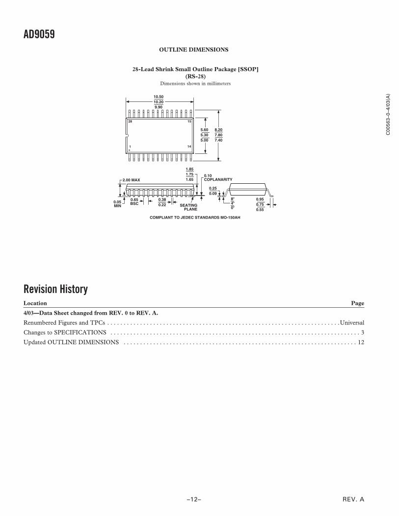
AD9059OUTLINE DIMENSIONS
28-Lead Shrink Small Outline Package [SSOP](RS-28)
Dimensions shown in millimeters
0.250.09
0.950.750.55
840
0.05MIN
1.851.751.652.00 MAX
0.380.22 SEATING
PLANE
0.65BSC
0.10COPLANARITY
28 15
141
10.5010.209.90
5.605.305.00
8.207.807.40
COMPLIANT TO JEDEC STANDARDS MO-150AH
Revision HistoryLocation Page
4/03—Data Sheet changed from REV. 0 to REV. A.
Renumbered Figures and TPCs . . . . . . . . . . . . . . . . . . . . . . . . . . . . . . . . . . . . . . . . . . . . . . . . . . . . . . . . . . . . . . . . . . . . . . .Universal
Changes to SPECIFICATIONS . . . . . . . . . . . . . . . . . . . . . . . . . . . . . . . . . . . . . . . . . . . . . . . . . . . . . . . . . . . . . . . . . . . . . . . . . . . . 3
Updated OUTLINE DIMENSIONS . . . . . . . . . . . . . . . . . . . . . . . . . . . . . . . . . . . . . . . . . . . . . . . . . . . . . . . . . . . . . . . . . . . . . . . 12