ad586 high precision 5 v reference data sheet (rev. g) · ad586 rev. g | page 6 of 16 pin...
TRANSCRIPT
High Precision5 V Reference
AD586
Rev. G Information furnished by Analog Devices is believed to be accurate and reliable. However, no responsibility is assumed by Analog Devices for its use, nor for any infringements of patents or other rights of third parties that may result from its use. Specifications subject to change without notice. No license is granted by implication or otherwise under any patent or patent rights of Analog Devices. Trademarks and registered trademarks are the property of their respective owners.
One Technology Way, P.O. Box 9106, Norwood, MA 02062-9106, U.S.A. Tel: 781.329.4700 www.analog.com Fax: 781.461.3113 © 2005 Analog Devices, Inc. All rights reserved.
FEATURES
Laser trimmed to high accuracy 5.000 V ±2.0 mV (M grade) Trimmed temperature coefficient
2 ppm/°C max, 0°C to 70°C (M grade) 5 ppm/°C max, −40°C to +85°C (B and L grades) 10 ppm/°C max, −55°C to +125°C (T grade)
Low noise, 100 nV/√Hz Noise reduction capability Output trim capability MIL-STD-883-compliant versions available Industrial temperature range SOICs available Output capable of sourcing or sinking 10 mA
GENERAL DESCRIPTION
The AD586 represents a major advance in state-of-the-art monolithic voltage references. Using a proprietary ion-implanted buried Zener diode and laser wafer trimming of high stability thin-film resistors, the AD586 provides outstanding perform-ance at low cost.
The AD586 offers much higher performance than most other 5 V references. Because the AD586 uses an industry-standard pinout, many systems can be upgraded instantly with the AD586.
The buried Zener approach to reference design provides lower noise and drift than band gap voltage references. The AD586 offers a noise reduction pin that can be used to further reduce the noise level generated by the buried Zener.
The AD586 is recommended for use as a reference for 8-, 10-, 12-, 14-, or 16-bit DACs that require an external precision reference. The device is also ideal for successive approximation or integrating ADCs with up to 14 bits of accuracy and, in general, can offer better performance than the standard on-chip references.
The AD586J, AD586K, AD586L, and AD586M are specified for operation from 0°C to 70°C; the AD586A and AD586B are specified for −40°C to +85°C operation; and the AD586S and AD586T are specified for −55°C to +125°C operation.
The AD586J, AD586K, AD586L, and AD586M are available in an 8-lead PDIP; the AD586J, AD586K, AD586L, AD586A, and AD586B are available in an 8-lead SOIC package; and the AD586J, AD586K, AD586L, AD586S, and AD586T are available in an 8-lead CERDIP package.
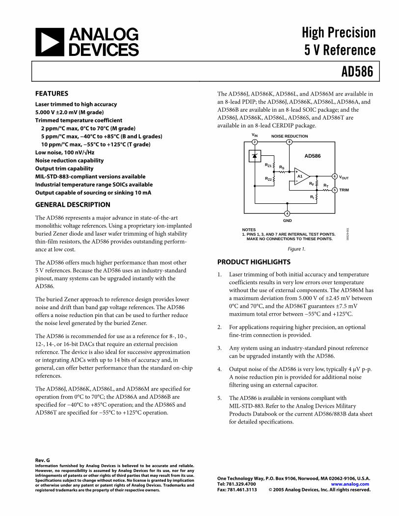
A1
RSRZ1
RZ2RF RT
RI
AD586
GND
VIN NOISE REDUCTION
VOUT
TRIM
NOTES1. PINS 1, 3, AND 7 ARE INTERNAL TEST POINTS.
MAKE NO CONNECTIONS TO THESE POINTS.
6
5
4
82
0052
9-00
1
Figure 1.
PRODUCT HIGHLIGHTS
1. Laser trimming of both initial accuracy and temperature coefficients results in very low errors over temperature without the use of external components. The AD586M has a maximum deviation from 5.000 V of ±2.45 mV between 0°C and 70°C, and the AD586T guarantees ±7.5 mV maximum total error between −55°C and +125°C.
2. For applications requiring higher precision, an optional fine-trim connection is provided.
3. Any system using an industry-standard pinout reference can be upgraded instantly with the AD586.
4. Output noise of the AD586 is very low, typically 4 µV p-p. A noise reduction pin is provided for additional noise filtering using an external capacitor.
5. The AD586 is available in versions compliant with MIL-STD-883. Refer to the Analog Devices Military Products Databook or the current AD586/883B data sheet for detailed specifications.

AD586
Rev. G | Page 2 of 16
TABLE OF CONTENTS Specifications..................................................................................... 3
AD586J, AD586K/AD586A, AD586L/AD586B ....................... 3
AD586M, AD586S, AD586T....................................................... 4
Absolute Maximum Ratings............................................................ 5
ESD Caution.................................................................................. 5
Pin Configurations and Function Descriptions ........................... 6
Theory of Operation ........................................................................ 7
Applying the AD586..................................................................... 7
Noise Performance and Reduction ............................................ 7
Turn-on Time................................................................................ 8
Dynamic Performance................................................................. 8
Load Regulation ............................................................................9
Temperature Performance............................................................9
Negative Reference Voltage from an AD586........................... 10
Using the AD586 with Converters ........................................... 10
5 V Reference with Multiplying CMOS DACs or ADCs ...... 11
Stacked Precision References for Multiple Voltages .............. 11
Precision Current Source .......................................................... 11
Precision High Current Supply ................................................ 11
Outline Dimensions ....................................................................... 13
Ordering Guide .......................................................................... 14
REVISION HISTORY
3/05—Rev. F to Rev. G Updated Format..................................................................Universal Split Specifications Table into Table 1 and Table 2....................... 3 Changes to Table 1............................................................................ 3 Added Figure 2 and Figure 4........................................................... 6 Updated Outline Dimensions ....................................................... 13 Changes to Ordering Guide .......................................................... 14
1/04—Rev. E to Rev. F Changes to ORDERING GUIDE ................................................... 3
7/03—Rev. D to Rev. E Removed AD586J CHIPS ..................................................Universal Updated ORDERING GUIDE........................................................ 3 Change to Figure 3 ........................................................................... 4 Updated Figure 12 ............................................................................ 7 Updated OUTLINE DIMENSIONS .............................................. 9
4/01—Rev. C to Rev. D Changed Figure 10 to Table 1 (Maximum Output Change in mV)............................................... 6
11/95—Revision 0: Initial Version
AD586
Rev. G | Page 3 of 16
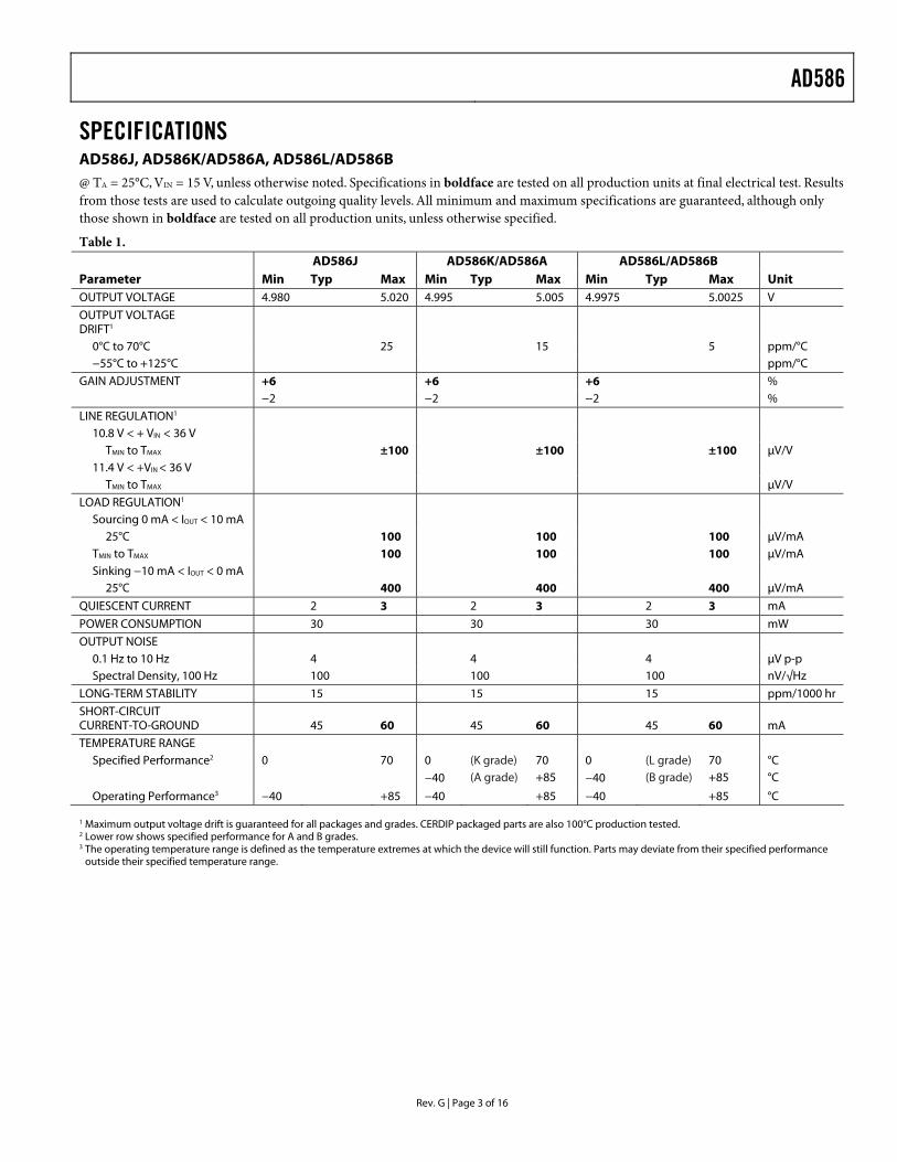
SPECIFICATIONS AD586J, AD586K/AD586A, AD586L/AD586B @ TA = 25°C, VIN = 15 V, unless otherwise noted. Specifications in boldface are tested on all production units at final electrical test. Results from those tests are used to calculate outgoing quality levels. All minimum and maximum specifications are guaranteed, although only those shown in boldface are tested on all production units, unless otherwise specified.
Table 1. AD586J AD586K/AD586A AD586L/AD586B Parameter Min Typ Max Min Typ Max Min Typ Max Unit OUTPUT VOLTAGE 4.980 5.020 4.995 5.005 4.9975 5.0025 V
OUTPUT VOLTAGE DRIFT1
0°C to 70°C 25 15 5 ppm/°C −55°C to +125°C ppm/°C
GAIN ADJUSTMENT +6 +6 +6 % −2 −2 −2 %
LINE REGULATION1 10.8 V < + VIN < 36 V
TMIN to TMAX ±100 ±100 ±100 µV/V 11.4 V < +VIN < 36 V
TMIN to TMAX µV/V
LOAD REGULATION1 Sourcing 0 mA < IOUT < 10 mA
25°C 100 100 100 µV/mA TMIN to TMAX 100 100 100 µV/mA Sinking −10 mA < IOUT < 0 mA
25°C 400 400 400 µV/mA
QUIESCENT CURRENT 2 3 2 3 2 3 mA
POWER CONSUMPTION 30 30 30 mW
OUTPUT NOISE 0.1 Hz to 10 Hz 4 4 4 µV p-p Spectral Density, 100 Hz 100 100 100 nV/√Hz
LONG-TERM STABILITY 15 15 15 ppm/1000 hr
SHORT-CIRCUIT CURRENT-TO-GROUND
45 60
45 60
45 60 mA
TEMPERATURE RANGE Specified Performance2 0 70 0
−40 (K grade) (A grade)
70 +85
0 −40
(L grade) (B grade)
70 +85
°C °C
Operating Performance3 −40 +85 −40 +85 −40 +85 °C
1 Maximum output voltage drift is guaranteed for all packages and grades. CERDIP packaged parts are also 100°C production tested. 2 Lower row shows specified performance for A and B grades. 3 The operating temperature range is defined as the temperature extremes at which the device will still function. Parts may deviate from their specified performance
outside their specified temperature range.

AD586
Rev. G | Page 4 of 16
AD586M, AD586S, AD586T @ TA = 25°C, VIN = 15 V, unless otherwise noted. Specifications in boldface are tested on all production units at final electrical test. Results from those tests are used to calculate outgoing quality levels. All minimum and maximum specifications are guaranteed, although only those shown in boldface are tested on all production units, unless otherwise specified.
Table 2. AD586M AD586S AD586T Parameter Min Typ Max Min Typ Max Min Typ Max Unit OUTPUT VOLTAGE 4.998 5.002 4.990 5.010 4.9975 5.0025 V
OUTPUT VOLTAGE DRIFT1
0°C to 70°C 2 ppm/°C −55°C to +125°C 20 10 ppm/°C
GAIN ADJUSTMENT +6 +6 +6 % −2 −2 −2 %
LINE REGULATION1 10.8 V < +VIN < 36 V
TMIN to TMAX ±100 µV/V 11.4 V < +VIN < 36 V
TMIN to TMAX ±150 ±150 µV/V
LOAD REGULATION1 Sourcing 0 mA < IOUT < 10 mA
25°C 100 150 150 µV/mA TMIN to TMAX 100 150 150 µV/mA Sinking −10 mA < IOUT < 0 mA
25°C 400 400 400 µV/mA
QUIESCENT CURRENT 2 3 2 3 2 3 mA
POWER CONSUMPTION 30 30 30 mW
OUTPUT NOISE 0.1 Hz to 10 Hz 4 4 4 µV p-p Spectral Density, 100 Hz
100 100 100 nV/√Hz
LONG-TERM STABILITY 15 15 15 ppm/1000 hr
SHORT-CIRCUIT CURRENT-TO-GROUND
45 60 45 60 45 60 mA
TEMPERATURE RANGE Specified Performance2 0 70 −55 +125 −55 +125 °C Operating Performance3 −40 +85 −55 +125 −55 +125 °C
1 Maximum output voltage drift is guaranteed for all packages and grades. CERDIP packaged parts are also 100°C production tested. 2 Lower row shows specified performance for A and B grades. 3 The operating temperature range is defined as the temperature extremes at which the device will still function. Parts may deviate from their specified performance
outside their specified temperature range.

AD586
Rev. G | Page 5 of 16
ABSOLUTE MAXIMUM RATINGS Table 3. Parameter Rating VIN to Ground 36 V Power Dissipation (25°C) 500 mW Storage Temperature −65°C to +150°C Lead Temperature (Soldering, 10 sec) 300°C Package Thermal Resistance
θJC 22°C/W θJA 110°C/W
Output Protection Output safe for indefinite short to ground or VIN.
Stresses above those listed under Absolute Maximum Ratings may cause permanent damage to the device. This is a stress rating only; functional operation of the device at these or any other conditions above those indicated in the operational section of this specification is not implied. Exposure to absolute maximum rating conditions for extended periods may affect device reliability.
ESD CAUTION ESD (electrostatic discharge) sensitive device. Electrostatic charges as high as 4000 V readily accumulate on the human body and test equipment and can discharge without detection. Although this product features proprietary ESD protection circuitry, permanent damage may occur on devices subjected to high energy electrostatic discharges. Therefore, proper ESD precautions are recommended to avoid performance degradation or loss of functionality.
AD586
Rev. G | Page 6 of 16
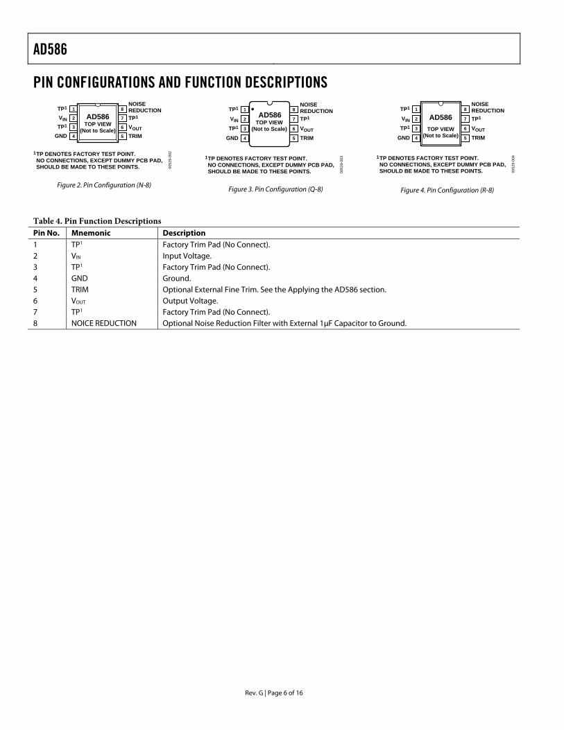
PIN CONFIGURATIONS AND FUNCTION DESCRIPTIONS
1TP DENOTES FACTORY TEST POINT.NO CONNECTIONS, EXCEPT DUMMY PCB PAD,SHOULD BE MADE TO THESE POINTS.
TP1 1
VIN 2
TP1 3
GND 4
NOISEREDUCTION8
TP17
VOUT6
TRIM5
AD586TOP VIEW
(Not to Scale)
0052
9-00
2
Figure 2. Pin Configuration (N-8)
1TP DENOTES FACTORY TEST POINT.NO CONNECTIONS, EXCEPT DUMMY PCB PAD,SHOULD BE MADE TO THESE POINTS. 00
529-
003
TP1 1
VIN 2
TP1 3
GND 4
NOISEREDUCTION8
TP17
VOUT6
TRIM5
AD586TOP VIEW
(Not to Scale)
Figure 3. Pin Configuration (Q-8)
1TP DENOTES FACTORY TEST POINT.NO CONNECTIONS, EXCEPT DUMMY PCB PAD,SHOULD BE MADE TO THESE POINTS. 00
529-
004
TP1 1
VIN 2
TP1 3
GND 4
NOISEREDUCTION8
TP17
VOUT6
TRIM5
AD586TOP VIEW
(Not to Scale)
Figure 4. Pin Configuration (R-8)
Table 4. Pin Function Descriptions Pin No. Mnemonic Description 1 TP1 Factory Trim Pad (No Connect). 2 VIN Input Voltage. 3 TP1 Factory Trim Pad (No Connect). 4 GND Ground. 5 TRIM Optional External Fine Trim. See the Applying the AD586 section. 6 VOUT Output Voltage. 7 TP1 Factory Trim Pad (No Connect). 8 NOICE REDUCTION Optional Noise Reduction Filter with External 1µF Capacitor to Ground.
AD586
Rev. G | Page 7 of 16
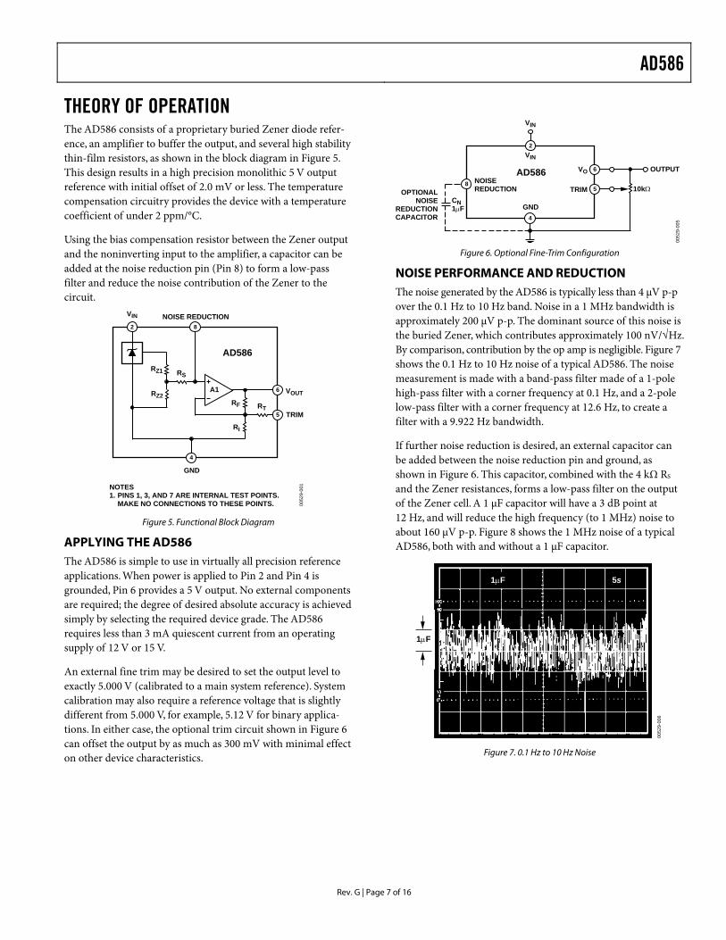
THEORY OF OPERATION The AD586 consists of a proprietary buried Zener diode refer-ence, an amplifier to buffer the output, and several high stability thin-film resistors, as shown in the block diagram in Figure 5. This design results in a high precision monolithic 5 V output reference with initial offset of 2.0 mV or less. The temperature compensation circuitry provides the device with a temperature coefficient of under 2 ppm/°C.
Using the bias compensation resistor between the Zener output and the noninverting input to the amplifier, a capacitor can be added at the noise reduction pin (Pin 8) to form a low-pass filter and reduce the noise contribution of the Zener to the circuit.
A1
RSRZ1
RZ2RF RT
RI
AD586
GND
VIN NOISE REDUCTION
VOUT
TRIM
NOTES1. PINS 1, 3, AND 7 ARE INTERNAL TEST POINTS.
MAKE NO CONNECTIONS TO THESE POINTS.
6
5
4
82
0052
9-00
1
Figure 5. Functional Block Diagram
APPLYING THE AD586 The AD586 is simple to use in virtually all precision reference applications. When power is applied to Pin 2 and Pin 4 is grounded, Pin 6 provides a 5 V output. No external components are required; the degree of desired absolute accuracy is achieved simply by selecting the required device grade. The AD586 requires less than 3 mA quiescent current from an operating supply of 12 V or 15 V.
An external fine trim may be desired to set the output level to exactly 5.000 V (calibrated to a main system reference). System calibration may also require a reference voltage that is slightly different from 5.000 V, for example, 5.12 V for binary applica-tions. In either case, the optional trim circuit shown in Figure 6 can offset the output by as much as 300 mV with minimal effect on other device characteristics.
AD586
GND
VIN
CN1µF
VO
TRIMOPTIONALNOISE
REDUCTIONCAPACITOR
VIN
NOISEREDUCTION
OUTPUT
10kΩ
6
5
2
4
8
0052
9-00
5
Figure 6. Optional Fine-Trim Configuration
NOISE PERFORMANCE AND REDUCTION The noise generated by the AD586 is typically less than 4 µV p-p over the 0.1 Hz to 10 Hz band. Noise in a 1 MHz bandwidth is approximately 200 µV p-p. The dominant source of this noise is the buried Zener, which contributes approximately 100 nV/√Hz. By comparison, contribution by the op amp is negligible. Figure 7 shows the 0.1 Hz to 10 Hz noise of a typical AD586. The noise measurement is made with a band-pass filter made of a 1-pole high-pass filter with a corner frequency at 0.1 Hz, and a 2-pole low-pass filter with a corner frequency at 12.6 Hz, to create a filter with a 9.922 Hz bandwidth.
If further noise reduction is desired, an external capacitor can be added between the noise reduction pin and ground, as shown in Figure 6. This capacitor, combined with the 4 kΩ RS and the Zener resistances, forms a low-pass filter on the output of the Zener cell. A 1 µF capacitor will have a 3 dB point at 12 Hz, and will reduce the high frequency (to 1 MHz) noise to about 160 µV p-p. Figure 8 shows the 1 MHz noise of a typical AD586, both with and without a 1 µF capacitor.
0052
9-00
6
1µF
5s1µF
Figure 7. 0.1 Hz to 10 Hz Noise

AD586
Rev. G | Page 8 of 16
0052
9-00
7
CN = 1µF
NO CN
50µS200µV
Figure 8. Effect of 1 µF Noise Reduction Capacitor on Broadband Noise
TURN-ON TIME Upon application of power (cold start), the time required for the output voltage to reach its final value within a specified error band is defined as the turn-on settling time. Two compo-nents normally associated with this are the time for the active circuits to settle, and the time for the thermal gradients on the chip to stabilize. Figure 9, Figure 10, and Figure 11 show the turn-on characteristics of the AD586. It shows the settling to be about 60 µs to 0.01%. Note the absence of any thermal tails when the horizontal scale is expanded to l ms/cm in Figure 10.
Output turn-on time is modified when an external noise reduc-tion capacitor is used. When present, this capacitor acts as an additional load to the current source of the internal Zener diode, resulting in a somewhat longer turn-on time. In the case of a 1 µF capacitor, the initial turn-on time is approximately 400 ms to 0.01% (see Figure 11).
0052
9-00
8
VIN
VOUT
10V 1mV
20µS
Figure 9. Electrical Turn-On
0052
9-00
9
VIN
VOUT
10V 5V 1mS
Figure 10. Extended Time Scale
0052
9-01
0
VIN
VOUT
10V 1mV 100mS
Figure 11. Turn-On with 1µF CN Characteristics
DYNAMIC PERFORMANCE The output buffer amplifier is designed to provide the AD586 with static and dynamic load regulation superior to less com-plete references.
Many ADCs and DACs present transient current loads to the reference, and poor reference response can degrade the per-formance of the converter.
Figure 12, Figure 13, and Figure 14 display the characteristics of the AD586 output amplifier driving a 0 mA to 10 mA load.
AD586 VL5V0V
VOUT
500Ω3.5V
0052
9-01
1
Figure 12. Transient Load Test Circuit

AD586
Rev. G | Page 9 of 16
0052
9-01
2
VL
VOUT
5V 50mV 1µS
Figure 13. Large-Scale Transient Response
0052
9-01
3
VL
VOUT
5V 1mV 2µS
Figure 14. Fine-Scale Setting for Transient Load
In some applications, a varying load may be both resistive and capacitive in nature, or the load may be connected to the AD586 by a long capacitive cable.
Figure 15 and Figure 16 display the output amplifier characteristics driving a 1000 pF, 0 mA to 10 mA load.
AD586 VL5V0V
VOUTCL1000pF 500Ω3.5V
0052
9-01
4
Figure 15. Capacitive Load Transient Response Test Circuit
0052
9-01
5
CL = 0
CL = 1000pF
5V 200mV 1µS
Figure 16. Output Response with Capacitive Load
LOAD REGULATION The AD586 has excellent load regulation characteristics. Figure 17 shows that varying the load several mA changes the output by a few µV. The AD586 has somewhat better load regulation per-formance sourcing current than sinking current.
–6 –4 –2
2 4 6 8 10 LOAD (mA)0
–500
–1000
500
1000
∆VOUT (µV)
0052
9-01
6
Figure 17. Typical Load Regulation Characteristics
TEMPERATURE PERFORMANCE The AD586 is designed for precision reference applications where temperature performance is critical. Extensive tempera-ture testing ensures that the device maintains a high level of performance over the operating temperature range.
Some confusion exists with defining and specifying reference voltage error over temperature. Historically, references have been characterized using a maximum deviation per degree Celsius, that is, ppm/°C. However, because of nonlinearities in temperature characteristics that originated in standard Zener references (such as “S” type characteristics), most manufacturers have begun to use a maximum limit error band approach to specify devices. This technique involves measuring the output at three or more different temperatures to specify an output volt-age error band.
AD586
Rev. G | Page 10 of 16
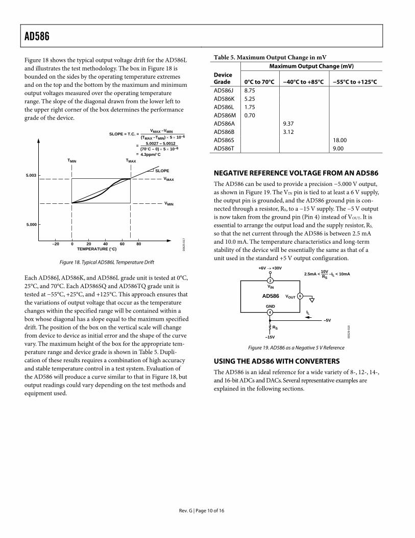
Figure 18 shows the typical output voltage drift for the AD586L and illustrates the test methodology. The box in Figure 18 is bounded on the sides by the operating temperature extremes and on the top and the bottom by the maximum and minimum output voltages measured over the operating temperature range. The slope of the diagonal drawn from the lower left to the upper right corner of the box determines the performance grade of the device.
–20 0 20 40 60 80
5.003
5.000
TEMPERATURE (°C)
VMIN
VMAX
VMAX –VMIN(TMAX –TMIN) × 5 × 10⁻⁶
SLOPE
TMIN TMAX
SLOPE = T.C. =
=
= 4.3ppm/°C
5.0027 – 5.0012(70°C – 0) × 5 × 10–6
0062
5-01
7
Figure 18. Typical AD586L Temperature Drift
Each AD586J, AD586K, and AD586L grade unit is tested at 0°C, 25°C, and 70°C. Each AD586SQ and AD586TQ grade unit is tested at −55°C, +25°C, and +125°C. This approach ensures that the variations of output voltage that occur as the temperature changes within the specified range will be contained within a box whose diagonal has a slope equal to the maximum specified drift. The position of the box on the vertical scale will change from device to device as initial error and the shape of the curve vary. The maximum height of the box for the appropriate tem-perature range and device grade is shown in Table 5. Dupli-cation of these results requires a combination of high accuracy and stable temperature control in a test system. Evaluation of the AD586 will produce a curve similar to that in Figure 18, but output readings could vary depending on the test methods and equipment used.
Table 5. Maximum Output Change in mV Maximum Output Change (mV) Device Grade 0°C to 70°C −40°C to +85°C −55°C to +125°C AD586J 8.75 AD586K 5.25 AD586L 1.75 AD586M 0.70 AD586A 9.37 AD586B 3.12 AD586S 18.00 AD586T 9.00
NEGATIVE REFERENCE VOLTAGE FROM AN AD586 The AD586 can be used to provide a precision −5.000 V output, as shown in Figure 19. The VIN pin is tied to at least a 6 V supply, the output pin is grounded, and the AD586 ground pin is con-nected through a resistor, RS, to a −15 V supply. The −5 V output is now taken from the ground pin (Pin 4) instead of VOUT. It is essential to arrange the output load and the supply resistor, RS, so that the net current through the AD586 is between 2.5 mA and 10.0 mA. The temperature characteristics and long-term stability of the device will be essentially the same as that of a unit used in the standard +5 V output configuration.
AD586
GND
+6V → +30V2.5mA < –IL < 10mA10V
RS
–5VRS
VOUT
VIN
IL
–15V
2
4
6
0052
9-01
8
Figure 19. AD586 as a Negative 5 V Reference
USING THE AD586 WITH CONVERTERS The AD586 is an ideal reference for a wide variety of 8-, 12-, 14-, and 16-bit ADCs and DACs. Several representative examples are explained in the following sections.

AD586
Rev. G | Page 11 of 16
5 V REFERENCE WITH MULTIPLYING CMOS DACs OR ADCs The AD586 is ideal for applications with 10- and 12-bit multiplying CMOS DACs. In the standard hookup, as shown in Figure 20, the AD586 is paired with the AD7545 12-bit multiplying DAC and the AD711 high speed BiFET op amp. The amplifier DAC configuration produces a unipolar 0 V to −5 V output range. Bipolar output applications and other operating details can be found in the individual product data sheets.
AD586
GND
VOUT
VIN
AD711K
0.1µF
0.1µF
–15V
0 V TO –5V
+15V
OUT 1
AGNDDGND
DB11TO DB0
C133pF
R268Ω
RFB
+15V
VDD
AD7545K
VREF
10kΩ
VOUT
TRIM
+15V
2018
196
5
4
2
3
1 2 7
4
6
3200
529-
019
Figure 20. Low Power 12-Bit CMOS DAC Application
The AD586 can also be used as a precision reference for multi-ple DACs. Figure 21 shows the AD586, the AD7628 dual DAC, and the AD712 dual op amp hooked up for single-supply opera-tion to produce 0 V to −5 V outputs. Because both DACs are on the same die and share a common reference and output op amps, the DAC outputs will exhibit similar gain TCs.
AD586GND AD712
OUT A
DGND
AGND
DAC A
DB0
DB7DATA
INPUTS
OUT BDAC B
RFB B
RFB AVREFA
VREFB
AD7628
VIN
VOUT A =0 TO –5V
VOUT B =0 TO –5V
VOUT
+15V +15V
6 4
4
7
14
2
5
317
1
19
20
2
4
0052
9-02
0
Figure 21. AD586 as a 5 V Reference for a CMOS
STACKED PRECISION REFERENCES FOR MULTIPLE VOLTAGES Often, a design requires several reference voltages. Three AD586s can be stacked, as shown in Figure 22, to produce 5.000 V, 10.000 V, and 15.000 V outputs. This scheme can be extended to any number of AD586s, provided the maximum load current is not exceeded. This design provides the addi-tional advantage of improved line regulation on the 5.0 V output. Changes in VIN of 18 V to 50 V produce output changes that are below the noise level of the references.
22V TO 46V
AD586
GND
VOUT
VIN
TRIM 10kΩ
AD586
GND
VOUT
VIN
TRIM
AD586
GND
VOUT
VIN
TRIM
10kΩ
10kΩ
15V
10V
5V
2
4
5
6
2
4
5
6
2
4
5
6
0052
9-02
1
Figure 22. Multiple AD586s Stacked for Precision 5 V, 10 V, and 15 V Outputs
PRECISION CURRENT SOURCE The design of the AD586 allows it to be easily configured as a current source. By choosing the control resistor RC in Figure 23, the user can vary the load current from the quiescent current (typically, 2 mA) to approximately 10 mA. The compliance volt-age of this circuit varies from about 5 V to 21 V, depending on the value of VIN.
AD586
GND
VOUT
VIN
5VRC
IL = + IBIAS
+VIN
RC(500Ω MIN)
2
4
6
0052
9-02
2
Figure 23. Precision Current Source
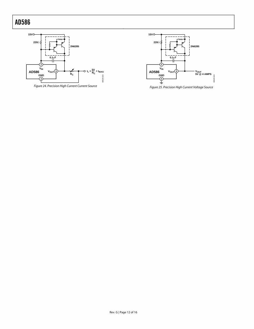
PRECISION HIGH CURRENT SUPPLY For higher currents, the AD586 can easily be connected to a power PNP or power Darlington PNP device. The circuit in Figure 24 and Figure 25 can deliver up to 4 amps to the load. The 0.1 µF capacitor is required only if the load has a significant capacitive component. If the load is purely resistive, improved high frequency supply rejection results can be obtained by removing the capacitor.
AD586
Rev. G | Page 12 of 16
AD586GND
VOUTVIN 5V
RCIL = + IBIAS
RC
0.1µF
15V
220Ω2N6285
2
6
4
0052
9-02
3
Figure 24. Precision High Current Current Source
VOUT5V @ 4 AMPS
AD586GND
VOUTVIN
0.1µF
15V
220Ω2N6285
2
6
4
0052
9-02
4
Figure 25. Precision High Current Voltage Source
AD586
Rev. G | Page 13 of 16
OUTLINE DIMENSIONS
COMPLIANT TO JEDEC STANDARDS MS-001-BA
0.022 (0.56)0.018 (0.46)0.014 (0.36)
SEATINGPLANE
0.015(0.38)MIN
0.210(5.33)MAX
PIN 1
0.150 (3.81)0.130 (3.30)0.115 (2.92)
0.070 (1.78)0.060 (1.52)0.045 (1.14)
8
1 4
5 0.280 (7.11)0.250 (6.35)0.240 (6.10)
0.100 (2.54)BSC
0.400 (10.16)0.365 (9.27)0.355 (9.02)
0.060 (1.52)MAX
0.430 (10.92)MAX
0.014 (0.36)0.010 (0.25)0.008 (0.20)
0.325 (8.26)0.310 (7.87)0.300 (7.62)
0.195 (4.95)0.130 (3.30)0.115 (2.92)
0.015 (0.38)GAUGEPLANE
0.005 (0.13)MIN
CONTROLLING DIMENSIONS ARE IN INCHES; MILLIMETER DIMENSIONS(IN PARENTHESES) ARE ROUNDED-OFF INCH EQUIVALENTS FORREFERENCE ONLY AND ARE NOT APPROPRIATE FOR USE IN DESIGN.CORNER LEADS MAY BE CONFIGURED AS WHOLE OR HALF LEADS.
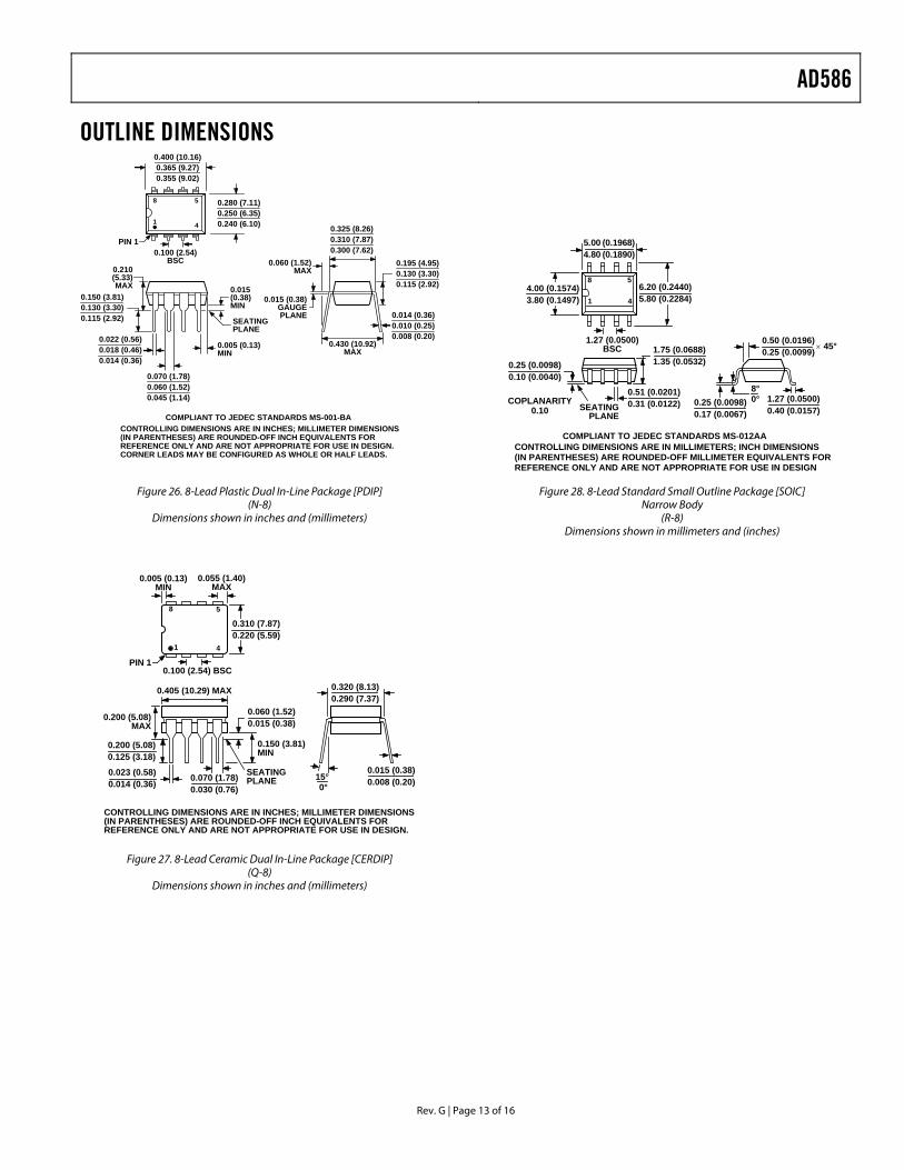
Figure 26. 8-Lead Plastic Dual In-Line Package [PDIP] (N-8)
Dimensions shown in inches and (millimeters)
CONTROLLING DIMENSIONS ARE IN INCHES; MILLIMETER DIMENSIONS(IN PARENTHESES) ARE ROUNDED-OFF INCH EQUIVALENTS FORREFERENCE ONLY AND ARE NOT APPROPRIATE FOR USE IN DESIGN.
1 4
58
0.310 (7.87)0.220 (5.59)
0.005 (0.13)MIN
0.055 (1.40)MAX
0.100 (2.54) BSC
15° 0°
0.320 (8.13)0.290 (7.37)
0.015 (0.38)0.008 (0.20)
SEATINGPLANE
0.200 (5.08)MAX
0.405 (10.29) MAX
0.150 (3.81)MIN
0.200 (5.08)0.125 (3.18)
0.023 (0.58)0.014 (0.36)
0.070 (1.78)0.030 (0.76)
0.060 (1.52)0.015 (0.38)
PIN 1
Figure 27. 8-Lead Ceramic Dual In-Line Package [CERDIP] (Q-8)
Dimensions shown in inches and (millimeters)
0.25 (0.0098)0.17 (0.0067)
1.27 (0.0500)0.40 (0.0157)
0.50 (0.0196)0.25 (0.0099)× 45°
8°0°
1.75 (0.0688)1.35 (0.0532)
SEATINGPLANE
0.25 (0.0098)0.10 (0.0040)
41
8 5
5.00 (0.1968)4.80 (0.1890)
4.00 (0.1574)3.80 (0.1497)
1.27 (0.0500)BSC
6.20 (0.2440)5.80 (0.2284)
0.51 (0.0201)0.31 (0.0122)COPLANARITY
0.10
CONTROLLING DIMENSIONS ARE IN MILLIMETERS; INCH DIMENSIONS(IN PARENTHESES) ARE ROUNDED-OFF MILLIMETER EQUIVALENTS FORREFERENCE ONLY AND ARE NOT APPROPRIATE FOR USE IN DESIGN
COMPLIANT TO JEDEC STANDARDS MS-012AA
Figure 28. 8-Lead Standard Small Outline Package [SOIC] Narrow Body
(R-8) Dimensions shown in millimeters and (inches)
AD586
Rev. G | Page 14 of 16
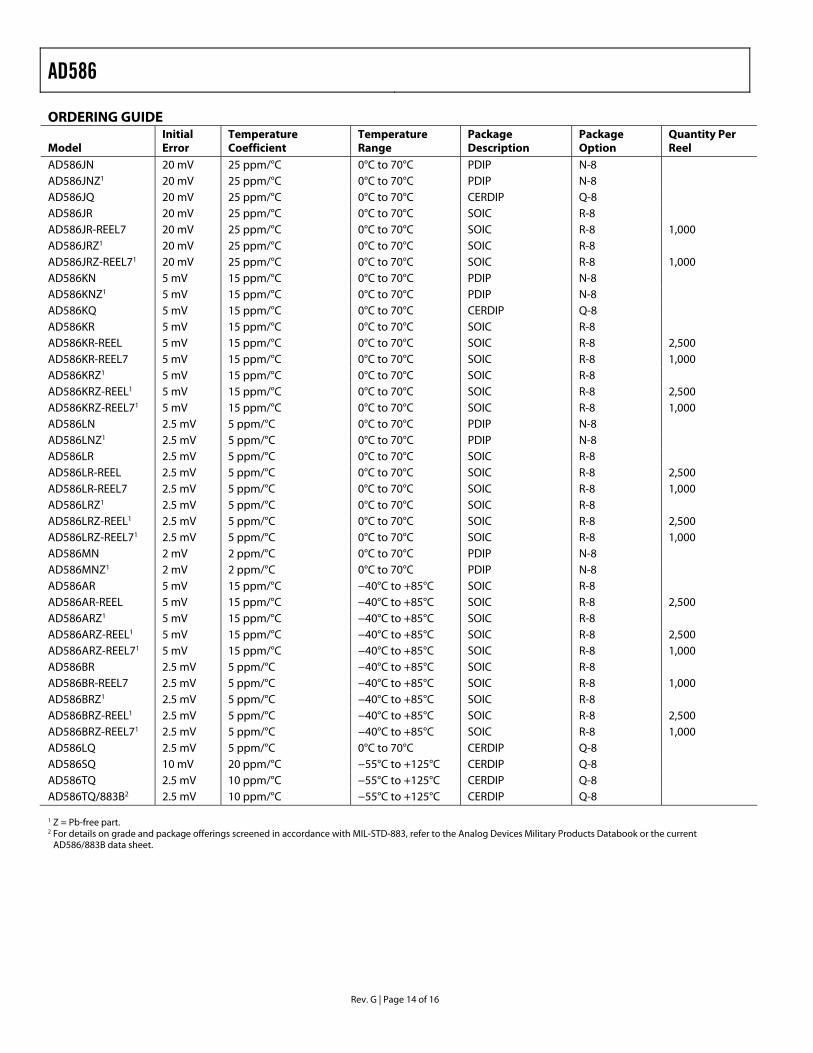
ORDERING GUIDE
Model Initial Error
Temperature Coefficient
Temperature Range
Package Description
Package Option
Quantity Per Reel
AD586JN 20 mV 25 ppm/°C 0°C to 70°C PDIP N-8 AD586JNZ1 20 mV 25 ppm/°C 0°C to 70°C PDIP N-8 AD586JQ 20 mV 25 ppm/°C 0°C to 70°C CERDIP Q-8 AD586JR 20 mV 25 ppm/°C 0°C to 70°C SOIC R-8 AD586JR-REEL7 20 mV 25 ppm/°C 0°C to 70°C SOIC R-8 1,000 AD586JRZ1 20 mV 25 ppm/°C 0°C to 70°C SOIC R-8 AD586JRZ-REEL71 20 mV 25 ppm/°C 0°C to 70°C SOIC R-8 1,000 AD586KN 5 mV 15 ppm/°C 0°C to 70°C PDIP N-8 AD586KNZ1 5 mV 15 ppm/°C 0°C to 70°C PDIP N-8 AD586KQ 5 mV 15 ppm/°C 0°C to 70°C CERDIP Q-8 AD586KR 5 mV 15 ppm/°C 0°C to 70°C SOIC R-8 AD586KR-REEL 5 mV 15 ppm/°C 0°C to 70°C SOIC R-8 2,500 AD586KR-REEL7 5 mV 15 ppm/°C 0°C to 70°C SOIC R-8 1,000 AD586KRZ1 5 mV 15 ppm/°C 0°C to 70°C SOIC R-8 AD586KRZ-REEL1 5 mV 15 ppm/°C 0°C to 70°C SOIC R-8 2,500 AD586KRZ-REEL71 5 mV 15 ppm/°C 0°C to 70°C SOIC R-8 1,000 AD586LN 2.5 mV 5 ppm/°C 0°C to 70°C PDIP N-8 AD586LNZ1 2.5 mV 5 ppm/°C 0°C to 70°C PDIP N-8 AD586LR 2.5 mV 5 ppm/°C 0°C to 70°C SOIC R-8 AD586LR-REEL 2.5 mV 5 ppm/°C 0°C to 70°C SOIC R-8 2,500 AD586LR-REEL7 2.5 mV 5 ppm/°C 0°C to 70°C SOIC R-8 1,000 AD586LRZ1 2.5 mV 5 ppm/°C 0°C to 70°C SOIC R-8 AD586LRZ-REEL1 2.5 mV 5 ppm/°C 0°C to 70°C SOIC R-8 2,500 AD586LRZ-REEL71 2.5 mV 5 ppm/°C 0°C to 70°C SOIC R-8 1,000 AD586MN 2 mV 2 ppm/°C 0°C to 70°C PDIP N-8 AD586MNZ1 2 mV 2 ppm/°C 0°C to 70°C PDIP N-8 AD586AR 5 mV 15 ppm/°C −40°C to +85°C SOIC R-8 AD586AR-REEL 5 mV 15 ppm/°C −40°C to +85°C SOIC R-8 2,500 AD586ARZ1 5 mV 15 ppm/°C −40°C to +85°C SOIC R-8 AD586ARZ-REEL1 5 mV 15 ppm/°C −40°C to +85°C SOIC R-8 2,500 AD586ARZ-REEL71 5 mV 15 ppm/°C −40°C to +85°C SOIC R-8 1,000 AD586BR 2.5 mV 5 ppm/°C −40°C to +85°C SOIC R-8 AD586BR-REEL7 2.5 mV 5 ppm/°C −40°C to +85°C SOIC R-8 1,000 AD586BRZ1 2.5 mV 5 ppm/°C −40°C to +85°C SOIC R-8 AD586BRZ-REEL1 2.5 mV 5 ppm/°C −40°C to +85°C SOIC R-8 2,500 AD586BRZ-REEL71 2.5 mV 5 ppm/°C −40°C to +85°C SOIC R-8 1,000 AD586LQ 2.5 mV 5 ppm/°C 0°C to 70°C CERDIP Q-8 AD586SQ 10 mV 20 ppm/°C −55°C to +125°C CERDIP Q-8 AD586TQ 2.5 mV 10 ppm/°C −55°C to +125°C CERDIP Q-8 AD586TQ/883B2 2.5 mV 10 ppm/°C −55°C to +125°C CERDIP Q-8
1 Z = Pb-free part. 2 For details on grade and package offerings screened in accordance with MIL-STD-883, refer to the Analog Devices Military Products Databook or the current
AD586/883B data sheet.

AD586
Rev. G | Page 15 of 16
NOTES

AD586
Rev. G | Page 16 of 16
NOTES
© 2005 Analog Devices, Inc. All rights reserved. Trademarks and registered trademarks are the property of their respective owners. C00529–0–3/05(G)