acmanual ww8
TRANSCRIPT
ENGINEERING 2-2 AC LAB MANUAL ONLY FOR REFERENCE
ENGINEERING 2-2 AC LAB MANUAL ONLY FOR REFERENCE
1
Expt: 1 AMPLITUDE MODULATION
AIM To study the operation of Amplitude modulator To calculate the modulation index of the Amplitude modulated wave. APPARATUS
Experimental boards of frequency modulation, dual trace CRO, AF generator. THEORY AMPLITUDE MODULATION It is a type of modulation in which the amplitude of high frequency sine wave (carrier) is varied in accordance with the instantaneous value of the modulating signal. Consider a sine wave signal Vm(t) with frequency f Vm(t) = ).2( tfSinEm ?? And another sine wave signal Vc (t) with frequency F Vc(t) = ).2( tFSinEc ??
In this signal Vm(t) is called modulating signal and the signal Vc(t) is called carrier signal. Vary the amplitude of the carrier Vc(t) after adding the modulating signal Vm(t) to Ec. You obtain a signal Vm(t) amplitude modulated, which can be expressed by: Vm(t) = ? ? ? ? ).2().2(.1).2(.2(. tFSintfSinmEctFSintfSinEmkEc ???? ?????? Percentage modulation signal is defined as the value:
100..EcEmK
m ?
With reference to fig 1.1C the modulation index m can be calculated in this way.
100minmaxminmax ?
???
EEEE
m
It is evident that larger the spectrum of the modulating signal, larger is the band width Bw occupied by the modulating signal. The resulted BW is equal to the double of the modulating signal: BW = 2.fm where fm=modulating signal frequency AMPLITUDE DEMODULATION The extraction of the modulating signal from an AM signal can be carried out using the envelop detector. Consider, in fact the AM signal shown in figure 2.1 and note that the modulating signal constitutes the envelop if the waveform reported. The most common envelop detector consists of a diode followed by RC filter. Its operation is analogous to the one of a half-wave rectifier, as the output voltage follows the

ENGINEERING 2-2 AC LAB MANUAL ONLY FOR REFERENCE
ENGINEERING 2-2 AC LAB MANUAL ONLY FOR REFERENCE
2
maximum values of the carrier. As the amplitude of the carrier is variable, by properly choosing R and C, the output of the detector can be faithfully reproduced. DISTORTIONS OF THE DETECTED SIGNAL
The demodulated signal can have two kinds of distortions: 1) If the time constant R.C is too small with respect to the time period of the carrier, the
envelop is approximated to a waveform affected by ripple, the more evident the lower value of R.C
2) If the time constant R.C too high with respect to the period of the modulating signal. The detected signal always follows the behavior of the envelop, but sometimes it takes an exponential decreasing law (distortion by diagonal cutting)
MINIMUM VALUE OF R.C (RIPPLE MINIMIZATION)
A first criterion for the choice of RC has the purpose to reduce the amplitude of the
ripple, which approximates the envelop to the minimum. To obtain this result the time constant RC must be very big with respect to the period T of the carrier, so to avoid an excessive discharge of C between two consecutive peaks of the AM signal. R.C>>T Fig. 2.4 shows two examples of detected signals, obtained with different values of R.C cannot be increased as you like, because too high values can cause distortion, too. MAXIMUM VALUE OF R.C (DISTORTION BY DIAGONAL CUTTING)
A further consideration for the proper choice of time constant R.C is detected
referring to fig 2.4. If the time constant is too high it can happen that, from a certain moment t1, the
output of the detector does not follow the envelope of the modulated signal any more, but continues to diminish with the discharge law of C, which is different to the law according to which the envelope varies. Then, the diode detector keeps, cut off until the instant t2, in which the outputs reach the envelope. In the interval (t2-t1), in fact, the output is constantly higher than the maximum values of the modulated signal, and the diode is inversely biased.
The distortion presented by the detected signal is known as Distortion by diagonal cutting.
The maximum value of RC is calculated supposing that the capacitor C discharges on the resistor R to a higher equal rhythm to the one in which the envelope of the modulated signal drops. The detected conditions as follows.
mmV
fCR
)1(.
max1.
2??
With m = modulation index: fmax = maximum frequency of the modulating signal Note that for m = 1 the condition cannot be satisfied, and so the detected signal will be certainly distorted.

ENGINEERING 2-2 AC LAB MANUAL ONLY FOR REFERENCE
ENGINEERING 2-2 AC LAB MANUAL ONLY FOR REFERENCE
3
LAST CONDITIONS ON THE CHOICE OF R.C IN THE ENVELOP DETECTOR
? To obtain a high detection efficiency the resistance R must be much higher than the differential resistance of rd of the diode (R>> rd).
? To minimize the ripple in the detected signal the product R.C must be much higher than the period T of the carrier (R.C >> T)
? To avoid distortion by diagonal cutting the product RC must be smaller or equal to a value, which depends on the modulating frequency, and on the modulation index. In the case of the modulating signal with variable amplitude and frequency, the maximum values of the frequency as well as of modulation index must be considered.
CIRCUIT DIAGRAM
Figure : a. AM Modulator
Figure : b. AM Demodulator
2N2369
100k?
4.7k?
100?
47k?
2.7k?
4.71? F
+
+
2N2369
4.71? F
N1 N2
Modulating Signal
Carrier
VCC = 12V
AM Output
OA 79
1KPF RL AM SIGNAL DEMODULATED
SIGNAL

ENGINEERING 2-2 AC LAB MANUAL ONLY FOR REFERENCE
ENGINEERING 2-2 AC LAB MANUAL ONLY FOR REFERENCE
4
100minmaxminmax
% ????
EEEE
m
CIRCUIT DESCRIPTION MODULATOR
The carrier is fed to transistor Q2 at its base of fig 1. This produces a collector current in Q2 at carrier frequency. The impedance in the collector circuit Q2 is decided by the transistor Q1. modulating signal is fed to the base of Q1, which changes the impedance offered by Q1 at the modulating frequency. The output is taken through a transformer coupling. When the modulating signal is zero Q1 offers a fixed impedance in the collector circuit of Q2, so that the output is a constant unmodulated carrier. As the modulating signal is applied to Q1 the impedance changes and the amplitude of the carrier at output also changes in accordance with above equation. DEMODULATOR
The circuit consists of a half wave rectifier followed by a capacitor input filter. Input to the circuit is a AM wave. The diode cuts off the negative going portion of the AM wave. Capacitor charges up to the peak of the carrier cycle through the low resistance of the rd (forward resistance of the diode) and then during the negative half cycle tried to discharge through relatively high resistance RL. Capacitor value is so chosen that the discharge is so small in the time between carrier half cycles. Hence the capacitor voltage tends to follow the envelop of the carrier and the voltage available across RL is simply the modulation envelop superimposed on the carrier. A dc level in the output comes because the current through diode flows in the form of pulses occurring at the peak of each carrier cycle. PROCEDURE
1) Make a study of the board. 2) Measure the internal carrier frequency by connecting the CRO at the carrier terminals. 3) Connect the carrier to the carrier input terminals, an AF generator to modulating
signal terminals and a CRO at the AM output terminals 4) Keeping the AF signal level to zero, switch on power supply of the board. Observe
that un-modulated carrier will appear on CRO screen. Measure its peak amplitude, Ec. 5) Keeping the CRO range to modulation frequency, slowly increase the AF generator
signal level and note down the amplitude Em. Amplitude modulated waveform will appear on CRO.
6) Compare the theoretical value of modulation given by EcEmm ?% ? 100, with the
practical value given by
TABULATION FOR MODULATION
S.No Base band frequency fm Emax Emin Em Ec
Practical
100minmaxminmax
% ????
EEEE
m
Theoretical
100% ??EcEmm

ENGINEERING 2-2 AC LAB MANUAL ONLY FOR REFERENCE
ENGINEERING 2-2 AC LAB MANUAL ONLY FOR REFERENCE
5
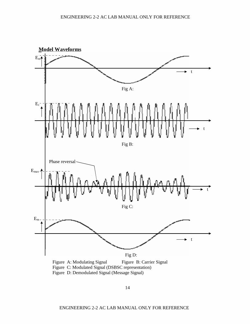
MODEL WAVEFORMS Figure A: Modulating Signal Figure B: Carrier Figure C: Modulated Signal Figure D: Diode Detector output Figure E: Demodulated Signal
Em
EC
Emax
Emin
t
t
t
t
t
Fig:A
Fig:B
Fig:C
Fig:D
Fig:E
Emax
Em

ENGINEERING 2-2 AC LAB MANUAL ONLY FOR REFERENCE
ENGINEERING 2-2 AC LAB MANUAL ONLY FOR REFERENCE
6
DEMODULATION
1) Connect the AM wave available at the output terminal to the demodulator input terminals.
2) Connect the load to the circuit. 3) Connect the CRO to the detector output terminals. See that with the variation of the
modulating signal amplitude the amplitude of the detected output changes and measure its frequency.
TABULATION FOR DEMODULATION S.No Modulation signal
voltage (Em) Demodulated signal voltage (Em)
Modulating signal frequency (fm)
Demodulated signal frequency
QUESTIONS:
1) Why modulation is an essential process of communication system? 2) Mention some applications of AM? 3) What are the distortions that are likely to be present in the demodulated output when
diode detector is used? 4) Explain how negative peak clipping occurs in the demodulated signal when diode
detector is used?

ENGINEERING 2-2 AC LAB MANUAL ONLY FOR REFERENCE
ENGINEERING 2-2 AC LAB MANUAL ONLY FOR REFERENCE
7
Expt:2 FREQUENCY MODULATION AND DEMODULATION
AIM 1. To study the process of frequency modulation and measure the modulation index. 2. To study the demodulation of FM signal. APPARATUS Experimental board of frequency modulation, dual traces CRO, AF generator. THEORY Frequency modulation is a system in which the frequency of the carrier is varied in accordance with the signal amplitude. Let’s assume for the moment that the carrier of the transmitter is at its resting frequency (no modulation) of 100MHz and we apply a modulating signal. The amplitude of the modulating signal will cause the carrier to deviate from this resting frequency by a certain amount. If we increase the amplitude of this signal, we will increase the deviation to a maximum of 75 kHz as specified by the FCC. If we remove the modulating voltage, the carrier shifts back to resting frequency (100MHz). From this we can say that the deviation of the carrier is proportional to the amplitude of the modulating voltage. The shift in the carrier frequency from its resting point compared to the amplitude of the modulating voltage is called the deviation ratio (a deviation ratio of 5 is the maximum) allowed in commercially broadcast FM) The rate at which the carrier shifts from its resting point to a nonresting point is determined by the frequency of the modulating signal. The interaction between the amplitude and frequency of the modulating signal on the carrier is complex and requires the use of Bessel’s function to analyze the results). If the modulating signal is 15kHz at a certain amplitude and the carrier shift is 75 kHz, the transmitter will produce eight significant sidebands. This is known as the maximum deviation ratio. Deviation ratio = (fdev (max) / fAF(max) ) If the frequency deviation of the carrier is known and the frequency of the modulating signal is known then Modulation index = fdev / fAF

ENGINEERING 2-2 AC LAB MANUAL ONLY FOR REFERENCE
ENGINEERING 2-2 AC LAB MANUAL ONLY FOR REFERENCE
8
CIRCUIT DESCRIPTION FM generator is basically a sine wave oscillator whose frequency could be varied by modulation signal. If the inductance or capacitance of a LC oscillator is varied then frequency modulation will result. In this board an integrated circuit called the function generator (8038) has been used for generation of FM. A ramp voltage is generated by charging a capacitor from a constant current source. A triangle waveform can be generated by alternate charging and discharging of a capacitor with constant current source and sink. The frequency of triangle waveform depends on the value of capacitance and the current of the source/sink. Now, if the capacitance is kept fixed and the current of the source and sink is varied according to the amplitude of a modulating signal then we shall get a waveform whose frequency is directly proportional to the amplitude of the modulating signal. This triangular waveform then can be converted into a sinusoidal one with the help of wave shaping circuits to get the true FM. Fig below shows the block diagram of the IC function generator. Two current sources, alternatively charge and discharge an external capacitor. When the current source 1 drives the triangle voltage above positive reference voltage, comparator 1 triggers the flip-flop. This connects the current source 2 which acts as a sink for the capacitor. This discharge rate is same as the charge rate. When triangle waveform falls below the negative reference level then the comparator 2 triggers the flip-flop and source 2 gets disconnected. The voltage across capacitor becomes triangle output. The sine wave is then obtained from the triangle wave through a converter circuit. The frequency of this sine wave is modulated by letting the modulating signal control the value of current source. Slope detection is one way of demodulating FM signals. The frequency selective nature of tuned circuit curve converts the frequency modulated carrier into an amplitude modulated one. After this the signal can be extracted simply by diode detector circuit which is used to detect an AM wave. The slope detector will work efficiently only if the frequency deviations are limited to the linear range of tuned curve.

ENGINEERING 2-2 AC LAB MANUAL ONLY FOR REFERENCE
ENGINEERING 2-2 AC LAB MANUAL ONLY FOR REFERENCE
9
CIRCUIT DIAGRAM
PROCEDURE STUDY OF MODULATION
1. Connect one input of the dual trace CRO between T1 and ground. 2. Switch on the power to the board. 3. Measure the frequency of sine wave carrier which appears on CRO screen. It shall be
around 20 kHz. Record this as fc. 4. Apply MOD signal at Em keeping control switch of CRO in DC position. 5. Note the variation in the frequency of the carrier as the amplitude of the DC is varied. 6. Next put the control switch in the sine wave position.
0.01uf N1 N2
2.2kpf
OA 79
4.7K C1
FM s ignal Demod Output
Figure b: FM Demodulator
IC 8
038
10k
Figure a: FM Modulator
-
+ +
U1
6
2
11
7
8
Modulation signal
VCC +12V
FM output

ENGINEERING 2-2 AC LAB MANUAL ONLY FOR REFERENCE
ENGINEERING 2-2 AC LAB MANUAL ONLY FOR REFERENCE
10
MODEL WAVEFORMS
Figure A: Modulating Signal Figure B: Carrier Figure C: Modulated Signal Figure D: Demodulated Signal
t
t
t
t
Em
v
v
Ec
Ec
Em
fmax fmin
Fig :A
Fig :B
Fig :C
Fig :D

ENGINEERING 2-2 AC LAB MANUAL ONLY FOR REFERENCE
ENGINEERING 2-2 AC LAB MANUAL ONLY FOR REFERENCE
11
7. Obtain a stationary wave form of FM signal on CRO screen by adjusting the amplitude and frequency of the modulating signal. At this stage use the other trace of the CRO to observe the modulating signal FM simultaneously.
8. Observing the FM wave form and modulating signal simultaneously on CRO screen, measure the frequency of the FM signal around the time of positive peak of the modulating signal. Record this frequency as fmax.
9. (fmax-fc) gives the frequency deviation. 10. Calculate the modulation index of the signal.
DEMODULATION
1. Generate FM signal using sine wave modulating signal. Keep the the modulating signal small.
2. Connect T1 to T2. FM signal gets connected to the demodulator circuit. 3. Observe the AM signal prior to the detector diode on CRO. 4. Connect the CRO at Demodulated output terminals. The original modulating signal
appears here after the envelop detection. Measure its frequency, is should be same as that of the modulating signal connected at Em.
5. Increase the amplitude of the modulating signal and observe its effect on the Demod output. At larger amplitudes distortion is produced. Give reasons for this in your notebook.
TABULATION MODULATION S.No.
Amplitude of Mod. signal(v)
A fmax(kHz)
B fmin(kHz)
? f=A-B
? = ? f/fm
DEMODULATION
S.No.
Mod-voltage (Em) in mv
Modulating Frequency in (kHz)
Demodulated Signal voltage
Demodulated Signal frequency

ENGINEERING 2-2 AC LAB MANUAL ONLY FOR REFERENCE
ENGINEERING 2-2 AC LAB MANUAL ONLY FOR REFERENCE
12
Expt: 3 BALANCED MODULATOR
AIM To study the process of Balanced Modulation and the corresponding waveforms. To
study the demodulation of Balanced modulated signal.
APPARATUS Experimental board of Balanced Modulator and Demodulator. AF signal generator for modulating signal, CRO.
CIRCUIT DIAGRAM
10u
C1
680
100 100
100
3.9 K 3.9 K
560
10K560
4.7K
P1
R1
470uf10
8 2
3
6
12145
4
1
Carrier
Mod.Signal
- Vcc
+ Vcc
Modulated Signal
200
10K
1.8K
3.9K 3.9K
C4 C5
C1
C2
R2
820
C3
C6
100100
2 3
5
6
12
144
1
10
8
Demod. output
Carrier
BM Signal
Vcc
IC 4196IC 1496
IC 1496
Figure :a. DSB-SC Modulator
Figure :b. DSB-SC Demodulator

ENGINEERING 2-2 AC LAB MANUAL ONLY FOR REFERENCE
ENGINEERING 2-2 AC LAB MANUAL ONLY FOR REFERENCE
13
THEORY Balanced Modulator is essentially an Amplitude modulation with no carrier power at output and is the heart of all the methods of single side band suppressed carrier modulation and demodulation. Any circuit which can produce in its output the product of two separate input signals can be used as a balance modulator. In balance modulation only sidebands are transmitted while carrier is fully suppressed. MODULATION
1. Make a study of the layout of the board. 2. Measure the internal carrier frequency and amplitude by CRO. 3. Connect the built in carrier to the carrier input terminal and AF generator (MOD
SIGNAL) between input signal terminal and ground terminal. 4. Keep AF signal level to zero and frequency approximately 4k Hz, switch ON
power supply on the board. 5. Keeping the CRO sweep in kHz/ m sec. Range, slowly increase the AF generator
signal level and obtain a stationery balance modulated waveform on CRO by adjusting the amplitude of the carrier and the amplitude and frequency of the modulating signal.
6. Trace the envelope of the modulated waveform from CRO screen.
DEMODULATION
1. Connect one output of the balance modulator to Mod I/P terminal and carrier of the modulator to the carrier terminal of the demodulator.
2. Connect the CRO at any one Demod output point. The demodulated signal appears here. Measure its frequency. It should be same as that of the modulating signal.
ENGINEERING 2-2 AC LAB MANUAL ONLY FOR REFERENCE
ENGINEERING 2-2 AC LAB MANUAL ONLY FOR REFERENCE
14
Model Waveforms
Figure A: Modulating Signal Figure B: Carrier Signal Figure C: Modulated Signal (DSBSC representation) Figure D: Demodulated Signal (Message Signal)
Em
t
Ec
t
Emax
t
Fig A:
Fig B:
Fig C:
Fig D:
Phase reversal
Em
t

ENGINEERING 2-2 AC LAB MANUAL ONLY FOR REFERENCE
ENGINEERING 2-2 AC LAB MANUAL ONLY FOR REFERENCE
15
PROCEDURE QUESTIONS What are the factors on which the bandwidth of a side band in balance
modulator output depends? TABULAR FORMS MODULATION S.No Mod. Freq (fm) Emax Emin Em Ec Practical % m Theoretical % m DEMODULATION
S.NO Modulating signal Demodulating signal Modulating frequency Demodulating frequency
Voltage Emin v voltage Em in v Fm in Hz Fm in Hz

ENGINEERING 2-2 AC LAB MANUAL ONLY FOR REFERENCE
ENGINEERING 2-2 AC LAB MANUAL ONLY FOR REFERENCE
16
R1
R2
BC 547
Rc
L
RE
100 u
10 u
10 u
+
CRO
+Signal Generator
Vcc
R 75k
C 1n
C2 10n
+Signal generator + 5CRO
Expt: 4
PRE -EMPHASIS& DE - EMPHASIS AIM
To draw the pre-emphasis and de-emphasis circuits and plot the frequency response of the circuit.
APPARATUS
Signal Generator, power supply, transistor, resistors, capacitors, DIB. THEORY
The noise triangle shows that noise has greater effect on the higher frequencies than on lower ones. Thus if higher frequencies were artificially boosted at the transmitter and correspondingly cut at the receiver, an improvement in noise immunity could be expected. This boosting of the higher modulating frequencies in accordance with a prearranged curve, is termed as pre-emphasis and the compensation at the receiver is called de-emphasis. CIRCUIT DIAGRAM PRE-EMPHASIS DE-EMPHASIS Model graph Pre-emphasis
Frequency
De- emphasis
Gai
n in
dB

ENGINEERING 2-2 AC LAB MANUAL ONLY FOR REFERENCE
ENGINEERING 2-2 AC LAB MANUAL ONLY FOR REFERENCE
17
PROCEDURE PRE-EMPHASIS
1. Design a self bias circuit. 2. Let T=75? sec. Let Rc= 1k? , select L T=L/RC 3. Connect the circuit as per the diagram. 4. Apply the input signal from a signal generator. 5. Vary the frequency of the input signal from 20Hz to 20kHz. 6. For each value of the input signal note down the output and calculate the gain. 7. Draw the graph between frequency Vs gain (Gain = 20 log (V0 / Vi ).
DE-EMPHASIS
1. Let T=RC, T=75 ? sec., Let C=1000pf, R= 75k? DESIGN Determine the value of Rc, Re, R1, R2 for the network for the operating point indicated. VCC = 12V ICQ = 5mA VCEQ = 6V VEN = VCC / 10 = 1.2 V RE = VEN / IE = VEN / IC = RC = VRC / IC = (VCC – VCEQ – VEN ) / IC VEN = VBE + VE = R2 ? (1 / 10) ? ? ? RE. Find R2, VBN = (R2 / (R1 + R2)) ? VCC find R1 TABULAR FORM PRE-EMPHASIS DE-EMPHASIS
S.No Freq O/P (V) Gain S.No Freq O/P (V) Gain (20 log(Vo/Vi) (20log(Vo/Vi)

ENGINEERING 2-2 AC LAB MANUAL ONLY FOR REFERENCE
ENGINEERING 2-2 AC LAB MANUAL ONLY FOR REFERENCE
18
100 K
Expt:5 CHARACTERISTICS OF MIXER
AIM To study the performance of mixer circuit (frequency converter)
APPARATUS
ACT 01, 03. ACT power supplies, CRO THEORY: The radio frequency signal (RF) detected by antenna is amplified by an RF amplifier and transferred, via a frequency mixer and a local oscillator (LO), to a lower and fixed frequency (Intermediate Frequency IF). The translation to a fixed and lower frequency than the received on enables to:
? Use a fixed band amplifier for the amplification of all the received signals, independently from their frequency.
? Operate on lower frequency signals The frequency translation is some times used in communication systems where for example, the modulation is carried out at an intermediate frequency having value lower than that of the effectively transmitted frequency.
As already said, to carry out the frequency translation a locally generated translation is necessary, called local oscillation, which interacts with the radio frequency signal so as to produce the new frequency.
If the oscillation is produced by the same operating circuit translation device, it is normally called as converter; in the reverse case we speak respectively of local oscillator and mixer. The frequency translation is differently indicated as frequency conversion, mixing, beating, and heterodyne process. The techniques used are many, and depend on the device used and on the operating frequencies. MIXER CIRCUiT

ENGINEERING 2-2 AC LAB MANUAL ONLY FOR REFERENCE
ENGINEERING 2-2 AC LAB MANUAL ONLY FOR REFERENCE
19
RF/FM RF IN OUT RF/FM LO OUT MIXER CONNECTIONS USING ACT 01 PROCEDURE CIRCUIT CONNECTIONS:
1. Connect the power supply with proper polarity to the kits ACT -01 &ACT -03 and switch it on.
2. Refer to the above block diagram and carry out the following connections and switch settings.
3. Carry out the following presetting in ACT -01 ? Keep the switch S3 in 1500 KHz position ? Using the pot P4 keep VCO1 frequency at 1000 KHz. ? Using the pot P5 keep VCO1 amplitude at 1 V p-p ? Using the pot P6 keep VCO2 frequency at 550 KHz ? Using the pot P7 keep VCO2 amplitude at 10omV p-p
4. Connect the output of VCO2 (act -01) RF/FM OUT post to the input of mixer (ACT -03) RF IN post
5. Connect the output of VCO1 (act -01) RF/FM OUT post to the other input of mixer (ACT -03) LO IN post.
MIXER (ACT 03)
P6 P7 Freq. LEVEL 0.2 VP-P
400 KHz – 1500KHz
VCO2 (ACT 01)
500KHz 1500KHz P4 P5 Freq. LEVEL 0.2 VP-P
VCO 1(ACT 01)

ENGINEERING 2-2 AC LAB MANUAL ONLY FOR REFERENCE
ENGINEERING 2-2 AC LAB MANUAL ONLY FOR REFERENCE
20
6. Connect the oscilloscope to the output post of the mixer IF OUT post and accurately vary the frequency of the local oscillator using the pot P4 until you detect a sine wave signal.
7. Measure the frequencies of the two input signals and the output signals, and check that the last is the difference of the first two fIF = fLO – fRF.

ENGINEERING 2-2 AC LAB MANUAL ONLY FOR REFERENCE
ENGINEERING 2-2 AC LAB MANUAL ONLY FOR REFERENCE
21
Expt:6 RECEIVER MEASUREMENTS
AIM 1. Study of AM superhetrodyne radio receiver. 2. To study the characteristics of AM superhetrodyne radio receiver. 3. To plot the I/P and O/P waveforms of detector E1 power amplifier.
APPARATUS AM superhetrodyne receiver multimeter, CRO.
THEORY The superheterodyne circuit is used in almost all the transistor radios (excepting a few used for receiving local stations). In this system the frequency of incoming signals are changed to a fixed frequency known as intermediate frequency IF. The main work of amplifying the signal and of selecting the desired station, is done in IF section. This permits higher amplification per stage and better selectivity. The block diagram of Radio receiver is shown in below. It consists of the following parts / stages.
1. frequency converter (Mixer and Oscillator) 2. I.F. amplifier 3. Detector 4. Audio Preamplifier 5. Driver 6. Output 7. Power supply
FREQUENCY CONVERTER It has two sections Mixer and Oscillator. Usually only one transistor is used for both sections. The oscillator produces oscillations at a frequency which is higher than the frequency of the station being received. The difference equals the intermediate frequency (I.F). Out of the signals interrupted by the aerial, the signals from the desired stations are selected by a tuned circuit at the input of the mixer stage. These signals and the oscillations from the oscillator are mixed by the mixer. The mixing of these signals results in the production of their sum (f1+f2) and the difference (f1-f2) frequencies. The difference is IF signal. It contains the same modulation as contained by the received signals. The IF signals are given to the IF amplifier.

ENGINEERING 2-2 AC LAB MANUAL ONLY FOR REFERENCE
ENGINEERING 2-2 AC LAB MANUAL ONLY FOR REFERENCE
22
IF AMPLIFIER It amplifies the IF signals. It provides a large part of the gain and selectivity. Two stages are used in this section to obtain the required amplification. Tuned transformers known as IFT are used as a collector load and for interstage coupling in the IF amplifier. The amplified IF signals are given to detector. DETECTOR The detector separates the audio signal from the modulated carrier. A diode is generally used for detection. AUDIO POWER AMPLIFIER The audio signals received from the detector are given to the audio preamplifier stage. This stage amplifies these signals and gives them to the driver stage. DRIVER The signals obtained from the preamplifier are not strong enough to drive the output stage. The driver stage further amplifies these signals and gives them to the output stage. OUTPUT STAGE The output stage amplifies the audio signals obtained from the driver and develops sufficient power to drive the loud speaker. To obtain maximum economy in battery consumption, pushpull output stages using two transistors in class B circuit is normally used. POWER SUPPLY Most of the transistor radios operate on a few cells/battery. The supply voltages from 3 to 9V are common. Some transistor radios can be operated from batteries as well as mains. In these transistor the mains voltage is converted into D.C. by diode rectifier.

ENGINEERING 2-2 AC LAB MANUAL ONLY FOR REFERENCE
ENGINEERING 2-2 AC LAB MANUAL ONLY FOR REFERENCE
23
GENERAL BLOCK DIAGRAM OF SUPERHETRODYNE RADIO RECEIVER Antenna (mixer + LO) Q1 Q2 Q3 D1 Q4 Q5 BF 194B BF 195C BF 195D 0A79 BC148A BC148B Q6,Q7 AC128 Loud Speaker BLOCK DIAGRAM OF AM/FM/SW RADIO RECEIVER PROCEDURE
1. Study the radio receiver kit. 2. Draw the block diagram of A.M. superhetrodyne receiver. 3. Identify all stages according to the block diagram and note down the RF, IF
transistors with their specifications.
FM Detector
FM IF amplifier
FM tuner
AM Detector
AM IF amplifier
AM tuner
Audio preamplifi
er
Audio O/P
Audio Driver
Frequency converter
1st IF amplifier
2nd IF amplifier
Detector
Audio preamplifier
Driver
Output
AGC
ENGINEERING 2-2 AC LAB MANUAL ONLY FOR REFERENCE
ENGINEERING 2-2 AC LAB MANUAL ONLY FOR REFERENCE
24
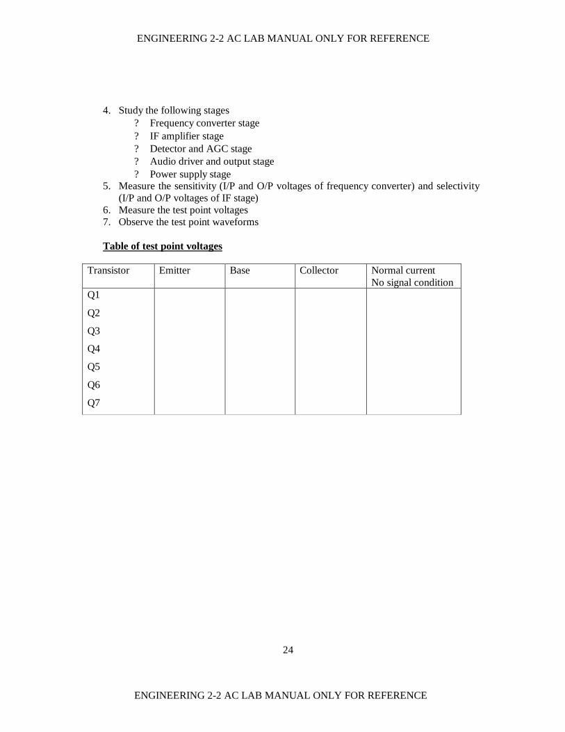
4. Study the following stages ? Frequency converter stage ? IF amplifier stage ? Detector and AGC stage ? Audio driver and output stage ? Power supply stage
5. Measure the sensitivity (I/P and O/P voltages of frequency converter) and selectivity (I/P and O/P voltages of IF stage)
6. Measure the test point voltages 7. Observe the test point waveforms Table of test point voltages
Transistor Emitter Base Collector Normal current No signal condition
Q1
Q2
Q3
Q4
Q5
Q6
Q7

ENGINEERING 2-2 AC LAB MANUAL ONLY FOR REFERENCE
ENGINEERING 2-2 AC LAB MANUAL ONLY FOR REFERENCE
25
IF SIGNAL AT COLLECTOR OF Q1 1KHz ? V 450KHz 0V IF SIGNAL AT COLLECTOR OF Q2 1KHz 450KHz IF SIGNAL AT COLLECTOR OF Q3 1KHz 450KHz 10mV 0V

ENGINEERING 2-2 AC LAB MANUAL ONLY FOR REFERENCE
ENGINEERING 2-2 AC LAB MANUAL ONLY FOR REFERENCE
26
Expt: 7 PHASE LOCKED LOOP
AIM To study design and find the lock range and capture range of phase locked loop
APPARATUS
Phase locked loop trainer board, function generator, CRO. CIRCUIT DIAGRAM THEORY The phase locked loop principle has been used in the applications such as FM tracking filters, frequency synthesized transmitters, FM demodulators, FSK decoders and generation of local oscillator frequencies in TV and FM tuners. This block diagram in its basic form contains 1. Phase detector, 2. Low pass filter 3. VCO (Voltage Controlled Oscillator). The function of phase detector is to compare the input signal fin and fout. The output of the phase detector is DC voltage and is often referred as the error voltage. The output signal of phase detector is fed to the input of low pass filter. The
R3
RT
C1C
CT
Vcc
10 8
7
6
4
5 19
2
3
- VEE
NE 565
Demodulated output
Reference outputInput Signal

ENGINEERING 2-2 AC LAB MANUAL ONLY FOR REFERENCE
ENGINEERING 2-2 AC LAB MANUAL ONLY FOR REFERENCE
27
function of the low pass filter is to remove the high frequencies and it allows only low frequency signals. It produces a DC level. The output of low pass filter is fed to the VCO. The VCO frequency is compared with the input signal and adjusted until it is equal to the input frequencies. If no signal is applied, the VCO starts to change until it equals the input frequency. And the PLL is said to be in phase locked state. PROCEDURE
1. Connect the circuit of PLL as shown in figure. 2. Measure the free running frequency of VCO at pin No. 4, with the input signal Vin set
equal to zero. Compare it with the calculated value = 0.25 RT.CT. 3. Now apply the input signal of 1V(P-P) square wave at 1 KHz at pin No.2. connect one
channel of CRO and display this signal on the scope. 4. Gradually increase the input signal frequency till the PLL is locked to the input
frequency. This frequency f1 gives the lower end of capture range. Go on increasing the input frequency, till the PLL tracks the input signal say to a frequency f2, gives the upper end of the lock range. If the frequency is increased further, the loop will get unlocked.
5. Now gradually decrease the input frequency till the PLL is again locked, this is the frequency f3, the upper end of the capture range. Keep on decreasing the input frequency until the loop is unlocked. This frequency f4 gives the lower end of lock range.
6. The lock range ).( 42 fff L ??? Compare it with the calculated value of 12
8.7 of
7. The capture range )( 13 fff C ??? . Compare it with the calculated value of capture
range. ???
???
???????
Cf
f LC 3106.32
.?
TABULATION fo.= --------------------.
S.No.
f1 in Hz
f2 in Hz
f3 in Hz
f4 in Hz
? fc theoretical
? fc practical
? fL
theoretical ? fL
practical

ENGINEERING 2-2 AC LAB MANUAL ONLY FOR REFERENCE
ENGINEERING 2-2 AC LAB MANUAL ONLY FOR REFERENCE
28
Expt: 8 SYNCHRONOUS AM DETECTOR
Aim
To study the performance of the synchronous am detector Apparatus
Modules ACT-01, ACT-02, power supplies for module, CRO THEORY In synchronous Am detector, also known as coherent detector, the signal modulated in amplitude is mixed to a coherent carrier signal and the result then, passes across a lowpass filter, which supplies the desired demodulated signal. The signal vM can be expressed by the following relation vM(t) = Vm(t).sin (2? F.t) Where Vm(t) = A.[1+m.sin(2? F.t)] is the amplitude of the envelop of the Am signal, and F
is the frequency of the carrier. If the AM signal is multiplied with a un-modulated signal which has the same frequency
and phase, the output of the multiplier is as composite signal Vo(t)which can be expressed in this way
Vo (t) = )].2.2cos(1.[.)].2sin().()].[.2sin(.[ tFVmKotFtVmtFAC ??? ?? Where Ko is considered as the gain of the multiplier circuit. Make the signal vo(t) pass across the low pass filter, to remove the component with 2F.t
frequency, the resulting signal Vout is Vout = Ko.Vm (t) Which corresponds to the Am detected signal. A PLL (Phase Locked Loop) system is generally used to regenerate a signal in the receiver,
which is exactly synchronous to the carrier of Am signal. In the applications where a high quality is required, the use of AM synchronous detector presents some important advantages with respect to the envelop detector ? low distortion ? capacity to properly demodulate the Am signal with high modulation depth, or with
quick variations of the modulation signal (as for example in pulse modulations) ? capacity to provide gain instead of attenuation introduced by diode.

ENGINEERING 2-2 AC LAB MANUAL ONLY FOR REFERENCE
ENGINEERING 2-2 AC LAB MANUAL ONLY FOR REFERENCE
29
P1 P2 Freq Level 1-10 K
Hz 0-2V
pp 0-1K
Hz
S1 S2
Function Generator (A
CT-01)
P1 P2 C
AR
. NU
LL level
BA
LAN
CED
MO
DU
LATO
R 1
(Act-02)
P1 C
AR
. NU
LL level
BA
LAN
CED
MO
DU
LATO
R 2
(Act-02)
LOW
PASS FILTER
P6 P7 FR
EQ
LEVEL
0-2V
pp 400 K
Hz- 1500K
Hz
SYN
CH
RO
NO
US A
M D
ETECTO
R

ENGINEERING 2-2 AC LAB MANUAL ONLY FOR REFERENCE
ENGINEERING 2-2 AC LAB MANUAL ONLY FOR REFERENCE
30
Figure A: Modulating Signal Figure B: Carrier Figure C: Modulated Signal Figure D: Balaced Moulator output at the detector Modulating Signal Figure E: Demodulated Signal
Em
t
EC
t
Emax
t
Emin
t
Emax
t
Emin
Em
Fig :A
Fig :B
Fig :C
Fig :D
Fig :E

ENGINEERING 2-2 AC LAB MANUAL ONLY FOR REFERENCE
ENGINEERING 2-2 AC LAB MANUAL ONLY FOR REFERENCE
31
PROCEDURE 1. Connect the power supply with proper polarities to kits and switch it on. 2. Refer to the figure and carry out the following connections and settings 3. In ACT-01
? Keep switch S1 in sine wave position ? Keep switch S2 in upper position (1-10KHz). ? Using pot P1 keep sine wave signal at 1KHz. ? Using pot P2 keep sine wave signal amplitude at 0.5 V pp ? Using pot P6 keep VCO2 frequency at 450KHz ? Using pot P1 keep VCO2 amplitude at 1Vpp.
4. In ACT-02 ? Keep BALANCED MODULATOR 1 CARRIER NULL rotated completely clockwise or slightly lower than clockwise pot P1 ? Keep BALANCED MODULATOR 1 LEVEL at 20mVpp using pot P2. ? Keep the BALANCED MODULATOR 2 CARRIER NULL in center position, so that the circuit operates as frequency converter (balanced modulator with suppressed carrier) using pot P3. ? Keep the BALANCED MODULATOR 2 LEVEL at maximum using pot P4.
5. Connect the output of function generator (ACT -01) OUT1 post to the input of balanced modulator 1 (ACT-02) SIGNAL IN post.
6. Connect the output of VCO2 (ACT -01) RF/FM OUT post to the input of balanced modulator 1 (ACT-02) CARRIER IN post.
7. Connect the output of balanced modulator1 (ACT -02) MOD OUT post to the input of balanced modulator 2 (ACT-02) SIGNAL IN post.
8. Connect the carrier of balanced modulator1 (ACT -02) CARRIER IN post to the input of balanced modulator 2 (ACT-02) CARRIER IN post.
9. Connect the output of balanced modulator 2 (ACT -02) MOD OUT post to the input of low pass filter (ACT-02) IN post.
10. Connect the CRO to the input of the demodulator post SIGNAL IN of the balanced modulator 2 and to the output post MOD OUT. The waveform detected across the output is the product between AM signal and the carrier that in the actual application is locally regenerated in the receiver. Note that this waveform consists of a frequency double the carrier, to which the waveform of the modulating signal is added.
11. The lowpass filter eliminates the high frequency component, supplying a clean detected signal. As the filter has a cutting frequency of 3.4 KHz, all the superior frequencies are attenuated.
12. Increase the modulation depth of AM signal and check that the detected signal does always faithfully follow the envelope. There is no distortion by diagonal cutting.

ENGINEERING 2-2 AC LAB MANUAL ONLY FOR REFERENCE
ENGINEERING 2-2 AC LAB MANUAL ONLY FOR REFERENCE
32
Expt: 9 SSB SYSTEM
Aim
To study the performance of the SSB system.
Apparatus
SSB transmitter and receiver kits, CRO.
Theory Single-sideband modulation is a form if amplitude modulation in which the carrier has
been cancelled out with a balanced modulator, and one of the sidebands has been removed by using any one of the filtering methods. The most common of these is the filter method. SSB is made possible because in “ordinary” AM, the carrier contains no information while two sidebands are mirror images of each other. From an information-carrying point of view, one of the sideband is superfluous. The main advantages of the SSB over DSBFC are that it requires much less power to transmit and occupies only half the bandwidth. Its main disadvantage is that it requires very much greater system frequency stability for satisfactory operation, and this feature is particularly demanding on receivers. Compared with DSBFC, SSB is decidedly a latecomer. Because of the receiver frequency stability requirement, SSB is not used in broadcasting, although sporadic work on compatible SSB goes on. In compatible SSB a proportion of the carrier would be transmitted and could be received by ordinary DSBFC receivers without undue distortion. Because of its power and bandwidth savings, SSB is used in a multitude of communication systems, notably long distance point-to point communication and mobile communications(including ship-to-shore and shore-to ship) at frequencies below about 30MHz. SSB is also a basic building block in frequency division multiplexing, a broad band communication technique used for multi channel communication in microwave links, terrestrial and submarine coaxial cables and satellite up- and down-links. The filter system The filter system is simplest system of three-after the balanced modulator the unwanted sideband is removed (actually heavily attenuated) by a filter. The filter may by LC, crystal, ceramic or mechanical, depending on the carrier frequency and other requirements. A block diagram of an SSB transmitter employing this system is shown below. The key circuits in this transmitter are balanced modulator and the sideband suppression filter. The special considerations involving sideband suppression will now be examined.

ENGINEERING 2-2 AC LAB MANUAL ONLY FOR REFERENCE
ENGINEERING 2-2 AC LAB MANUAL ONLY FOR REFERENCE
33
Such a filter must have a flat bandpass and extremely high attenuation outside the bandpass. There is no limit on this; the higher the attenuation, the better. In radio communication systems, the frequency range used for voice is 300 to about 2800 Hz in most cases. If it is required to suppress the lower sideband and if the transmitting frequency is f, then the lowest frequency that must be passed through this filter without attenuation is f + 300Hz, whereas the highest frequency that must be fully attenuated is f – 300Hz. In other words, the filter’s response must change from zero attenuation to full attenuation over a range of only 600Hz. If the transmitting frequency is much above 10MHz, this is virtually impossible. This situation becomes even worse if lower modulating frequencies are employed, such as the 50Hz minimum in AM broadcasting. In order to obtain a filter response curve with skirts as steep as those suggested above, the Q of the tuned circuits used must be very high. As the transmitting frequency is raised, so must the Q be raised, until a situation is reached where the necessary Q is so high that there is no practicable method of achieving it. Looking at the situation from the other end, we find that there must be an upper frequency limit for any type of filter circuit used. It has been found, for instance, that multistage LC filters cannot be used for RF values such greater than about 100kHz. Above this frequency the attenuation outside the bandpass is sufficient. LC filters may still be encountered in currently used HF equipment, but they have otherwise tended to be superseded by crystal, ceramic or mechanical filters, mainly because of the bulky size of components and great improvements in mechanical filters. Mechanical filers have been used at frequencies up to 500 kHz, and crystal or ceramic filters up to about 20MHz. Of the three major types of SSB filters, the mechanical filters seems to be the one with the best all-around properties, small size, good bandpass, very good attenuation characteristics and an adequate upper frequency limit are its chief advantages. Crystal or ceramic filters may be cheaper, but are preferably at frequencies above 1 MHz. All these filters ( even the crystal ) have the same disadvantage –their maximum operating frequency is below the usual transmitting frequencies. This is the reason for the balanced mixer shown in below (it is very much like a balanced modulator, except that the sum frequency is much farther from the crystal oscillator frequency than the USB was from the carrier, so that it can be selected with a tuned circuit.) In this mixer, the frequency of the crystal oscillator or synthesizer is added to the SSB signal from the filter, the frequency thus being raised to the value desired for transmission. Such an arrangement also allows the transmitter to be tunable. If the transmitting frequency is much higher than the operating frequency of the sideband filter, then two stages of mixing will be required. It becomes too difficult to filter out the unwanted frequencies in the output of the mixer. It might be noted that the mixer is followed by linear amplifiers. The reason is that the amplitude of the SSB signal is variable and must be fed to a class C amplifier, which would distort it. A class B RF amplifier (Push-Pull) is used instead because it is more efficient than
ENGINEERING 2-2 AC LAB MANUAL ONLY FOR REFERENCE
ENGINEERING 2-2 AC LAB MANUAL ONLY FOR REFERENCE
34
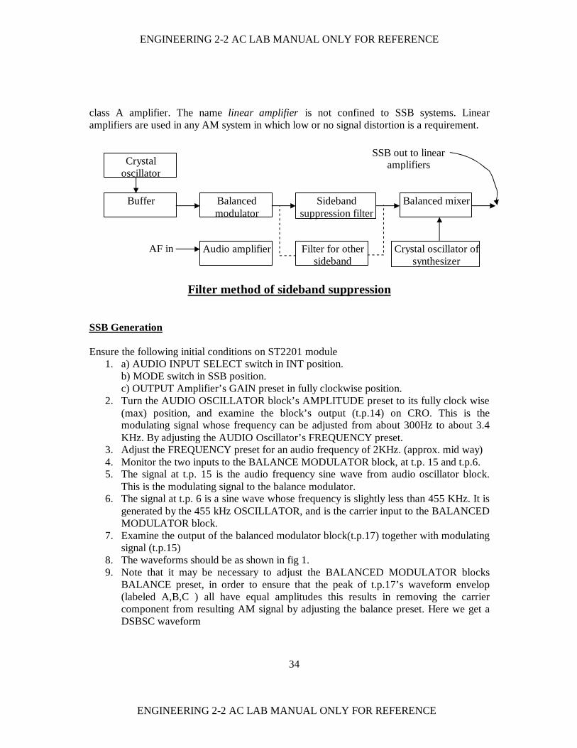
class A amplifier. The name linear amplifier is not confined to SSB systems. Linear amplifiers are used in any AM system in which low or no signal distortion is a requirement.
Filter method of sideband suppression
SSB Generation Ensure the following initial conditions on ST2201 module
1. a) AUDIO INPUT SELECT switch in INT position. b) MODE switch in SSB position. c) OUTPUT Amplifier’s GAIN preset in fully clockwise position. 2. Turn the AUDIO OSCILLATOR block’s AMPLITUDE preset to its fully clock wise
(max) position, and examine the block’s output (t.p.14) on CRO. This is the modulating signal whose frequency can be adjusted from about 300Hz to about 3.4 KHz. By adjusting the AUDIO Oscillator’s FREQUENCY preset.
3. Adjust the FREQUENCY preset for an audio frequency of 2KHz. (approx. mid way) 4. Monitor the two inputs to the BALANCE MODULATOR block, at t.p. 15 and t.p.6. 5. The signal at t.p. 15 is the audio frequency sine wave from audio oscillator block.
This is the modulating signal to the balance modulator. 6. The signal at t.p. 6 is a sine wave whose frequency is slightly less than 455 KHz. It is
generated by the 455 kHz OSCILLATOR, and is the carrier input to the BALANCED MODULATOR block.
7. Examine the output of the balanced modulator block(t.p.17) together with modulating signal (t.p.15)
8. The waveforms should be as shown in fig 1. 9. Note that it may be necessary to adjust the BALANCED MODULATOR blocks
BALANCE preset, in order to ensure that the peak of t.p.17’s waveform envelop (labeled A,B,C ) all have equal amplitudes this results in removing the carrier component from resulting AM signal by adjusting the balance preset. Here we get a DSBSC waveform
Crystal oscillator
Buffer Balanced modulator
Sideband suppression filter
Balanced mixer
Crystal oscillator of synthesizer
Filter for other sideband
Audio amplifier
SSB out to linear amplifiers
AF in

ENGINEERING 2-2 AC LAB MANUAL ONLY FOR REFERENCE
ENGINEERING 2-2 AC LAB MANUAL ONLY FOR REFERENCE
35
10. The DSBSC waveform is now passed on to the CERAMIC FILTER block whose purpose is to pass the upper sideband but to lock the lower sideband.
11. Monitor the output of the CERAMIC BANDPASS FILTER block at t.p.20. Note that the envelope of the signal a t.p. 20 now has fairly constant amplitude. If the amplitude is not reasonably constant adjust the BALANCE preset in the BALANCE MODULATOR block to minimize the variations in the signal’s amplitude.
12. Now observe the CERAMIC BANDPASS Filter’s output signal(t.p.20) and note that the signal is good clean sine wave , indicating that the filter is passed upper sideband only.
13. Turn the AUDIO OSCILLATOR block’s FREQUENCY preset throughout its range. Note that for most audio frequencies, the waveform is a good, clean sine wave, indicating that the lower sideband has been completely rejected by the filter. For low audio frequencies the signal is not such a pure sinusoid. This is because the upper and lower sidebands are now very close to each other.
14. Note that, by passing only the upper sideband, the frequency of the modulating signal is shifted by an amount equal to carrier frequency.
15. Adjust the audio oscillators frequency to 2KHz, turn the block’s AMPLITUDE preset to min position, and note that the amplitude of the signal at CERAMIC BANDPASS Filter’s output drops to zero. This highlights one on the main advantages of SSB amplitude modulation if there is no modulating signal , then the amplitude of the SSB waveform drops to zero, so that there is no power wastage.
16. The CERAMIC BANDPASS FILTER is used here to pass only the upper sideband, but to attenuate the lower sideband which is produced during the AM modulation. But the disadvantage of this type of filter is that the range of pass band is fixed during the filter’s manufacture and cannot be altered subsequently. The filter we are using here has a pass band which is centered at 455 kHz.
17. The ST2201/ST2202 receiver will accept radio-frequency signals in the AM broadcast band i.e. signals which fall in the frequency range of 525 kHz. To overcome this problem the narrow band of frequencies must be shifted up, so that it falls within AM broad cast range. This frequency shifting operation is performed by the BALANCED MODULATOR & BANDPASS FILTER CIRCUIT 2, block, which contains a balanced modulator followed by a tuned circuit.
18. Now monitor the output of the BALANCED MODULATOR & BANDPASS FILTER CIRCUIT 2 block at t.p.22, and check that the waveform is pure sine wave of frequency approximately 1.45 MHz. check that the waveform is reasonably good sinusoid for audio modulating frequencies. If this is not the case adjust the BALANCE preset in BALANCED MODULATOR & BANDPASS FILTER CIRCUIT 2 block to remove the residual carrier frequency at 1MHz.
19. Now the signal has been shifted to AM broad cast range of 525kHz to 1.6MHz. 20. Now monitor the frequency at t.p 22. Reduce the amplitude of the modulating signal
to zero and observe that the output at t.p.22 follows the drops to zero. 21. This is the SSB signal which is applied to antenna for transmission.

ENGINEERING 2-2 AC LAB MANUAL ONLY FOR REFERENCE
ENGINEERING 2-2 AC LAB MANUAL ONLY FOR REFERENCE
36
SSB reception 1. Position the ST 2201 & ST2202 modules, with the ST2201 board on the left, and a
gap of about three inches. 2. ensure the following initial conditions exists on the ST2201 module
a) AUDIO Oscillator’s AMPLITUDE preset in fully clockwise position. b) AUDIO INPUT SELECT switch in INT position. c) MODE switch in SSB position. d) OUTPUT Amplifier’s GAIN preset in fully clockwise position. e) TX OUTPUT SELECT switch in ANT position. f) AUDIO Amplifier’s VOLUME preset in fully counter-clockwise position. g) SPEAKERS switch in ON position. h) On board antenna in vertical position, fully extended.
3. Ensure the following initial conditions exist on the ST2202 module. a) RX INPUT SELECT switch in ANT position. b) RF Amplifier’s TUNED CIRCUIT SELECT switch in INT position. c) RF Amplifier’s GAIN preset in fully clockwise position. d) AGC switch in OUT position. e) DETECTOR switch in PRODUCT position. f) AUDIO Amplifier’s VOLUME preset in fully counter clockwise position. g) SPEAKERS switch in ON position. h) BEAT FREQUENCY OSCILLATOR switch in ON position. i) On-board antenna in vertical position fully extended.
4. Turn on the power to the modules. 5. On the ST 2201 module, examine the transmitter’s output signal (t.p.13), and make
sure that the signal is reasonably good sine wave. 6. Turn the ST2201’s amplitude preset (in AUDIO OSCILLATOR block) to its fully
counter clockwise (minimum) position, and note that the amplitude if the monitored signal from ST2201 (at t.p.13) drops to zero. Which illustrates that SSB waveform contains no carrier-power. Now return the amplitude to its maximum position.
7. Since ST2201’s TX OUTPUT SELECT is in the ANT position the SSB signal is fed to the antenna.
8. On the ST2202 module, monitor the output of the IF AMPLIFIER 2 block (t.p.28) and turn the tuning dial until the amplitude of the monitored signal is at its greatest.
9. Since the incoming signal has no carrier component, the receiver AGC circuit cannot make use of incoming carrier amplitude in order to control the gain of the receiver. This means that the receiver’s AGC CIRCUIT cannot be used for SSB reception, and must be switched out.
10. Turn the GAIN preset in ST2201’s OUTPUT AMPLIFIER block, so that the preset’s arrowhead is horizontal and pointing to the left. This ensures that the amplitude of the transmitted SSB signal is small.

ENGINEERING 2-2 AC LAB MANUAL ONLY FOR REFERENCE
ENGINEERING 2-2 AC LAB MANUAL ONLY FOR REFERENCE
37
11. On ST 2202 module, fine tune the tuning dial until the amplitude of the monitored signal is at its greatest.
12. The receiver’s BFO produces a sine wave at the IF frequency of 455 KHz. This 455KHZ is the input to the receiver’s PRODUCT DETECTOR block, where it is mixed with the SSB from IF amplifier.
13. The PRO0DUCT DETECTOR block mixes the output from the BFO with the output from the IF amplifier block. Mixing process results in the generation of two new frequency components: 1) sum of two frequencies 2) difference of those two.
14. The low-pass filter at the output of the PRODUCT DETECTOR accepts the difference frequency. This audio frequency is then converted into sound by the receivers AUDIO AMPLIFIERS BLOCK.
15. To demodulate out the incoming signal, we tune the Receiver’s LOCAL OSCILLATOR so that the output frequency range from IF AMPLIFIER 2 is slightly below the 455KHz BFO frequency, such that the difference frequency generated by the PRODUCT DETECTOR is same that of the modulating frequency. Then as the frequency of the modulating signal changes the PRODUCT DETECTOR should follow it.
16. On ST 2202/1 modules adjust the volume preset so that the receiver’s output is clearly audible.
17. Slowly turn the tuning dial and notice that the tone at the receiver’s output changes. On the ST2201 module turn the volume preset clockwise, until you can hear the tone of the audio oscillator’s output signal. Find the position of the TUNING dial till two tones are approximately same (i.e. of transmitter and receiver).
18. Now turn the frequency preset in ST2001’s AUDIO OSCILLATOR lock, throughout its range noting that the frequency of the tone generated by the ST2202 remains close to that generated by ST2201 for all preset positions.
19. connect the CRO at the output of Audio Oscillator block and at the output of the receiver and note if there is any frequency deviation in these signals.

ENGINEERING 2-2 AC LAB MANUAL ONLY FOR REFERENCE
ENGINEERING 2-2 AC LAB MANUAL ONLY FOR REFERENCE
38
Model waveforms Figure :A Modulating Signal at t.p.15 Figure :B Carrier at t.p. 6 Figure :C Balanced modulator o/p at t.p. 17 Figure :D Balanced modulator and bandpass filter circuit 2 o/p at t.p.22 Figure :E Demodulated signal at t.p. 15
a ba
ca
da
Fig : A
Fig : B
Fig : C
Fig : D
Fig : E
Em
t
EC
t
Em
t
Em
t
Em
t

ENGINEERING 2-2 AC LAB MANUAL ONLY FOR REFERENCE
ENGINEERING 2-2 AC LAB MANUAL ONLY FOR REFERENCE
39
Expt:10 SPECTRUM ANALYZER
AIM To analyze the AM and FM waveform using Spectrum Analyzer. The oscilloscope is the most common device used to display the signals, with time as x-axis. The signal which require time as x-axis, to display them are time domain signals. The signals which require frequency as x-axis, to display them are called frequency domain signals. Frequency domain display of signal consists of information of energy distributed of the signal. The analysis of such a frequency domain display of the signal is called spectral analysis of the signal. Thus the study of the energy distribution across the frequency spectrum if a given signal is defined as the spectral analysis. The instrument which graphically provides the energy distribution of a signal as a function of frequency on its CRT is called spectrum analyzer. It provides a calibrated graphical display with the frequency on horizontal axis and the signal component on the vertical axis, the sinusoidal components of which, the signal is made up of, are displayed as the vertical lines against frequency coordinates. The frequency of each vertical line gives the absolute amplitude if the component while the horizontal location gives that particular frequency. Introduction The analysis of electrical signals is a fundamental problem for many engineers and scientists. Even if the immediate problem is not electrical, the basic parameters of interest are often changed into electrical signals by means of transducers. The rewards for transforming physical parameters to electrical signals are great, as many instruments are available for the analysis of electrical signals in the time and frequency domain. The traditional way of observing electrical signals is to view them in time domain using oscilloscope. The time domain is used to recover relative timing and phase information which is needed to characterize electrical circuit behavior. How ever, not all circuit can be uniquely characterized from just time domain information. Circuit elements such as amplifiers, oscillators, mixers, modulators, detectors and filters are best characterized by their frequency response information. This frequency information is best obtained by viewing electrical signals in frequency domain. To display the signal in the frequency domain requires a device that can discriminate between frequency domains is the spectrum analyzer. It graphically displays the voltage or power as a function of frequency on a CRT. In the time domain, all frequency components of a signal are seen summed together. In the frequency domain, complex signals are separated in to their frequency components, and power level at each frequency is displayed. The frequency domain is a graphical representation of signal amplitudes as a function of frequency. the frequency domain contains information not found in time domain.

ENGINEERING 2-2 AC LAB MANUAL ONLY FOR REFERENCE
ENGINEERING 2-2 AC LAB MANUAL ONLY FOR REFERENCE
40
Types of spectrum analyzers There are two basic types of spectrum analyzers, swept-tuned and real time analyzers. The swept-tuned analyzers are tuned by electrically sweeping them over their frequency range. Therefore the frequency components of a spectrum are sampled sequentially in time. This enables periodic and random signals to be displayed, but makes it impossible to display transient response. Real time analyzers, on the other hand, simultaneously display the amplitude of all signals in the frequency range of the analyzer: hence the name real-time. This preserves the time dependency between signals which permits information to be displayed. Real time analyzers are capable of displaying transient response as well as periodic and random signals. The swept tuned analyzers are usually of the trf (tuned radio frequency) or superheterodyne type. A trf analyzer consists of a frequency range, a detector to produce vertical deflection on a CRT, and a horizontal scan generator used to synchronize the tuned frequency to the CRT horizontal deflection. It is a simple, inexpensive analyzer with wide frequency coverage, but lacks resolution and sensitivity. Because trf analyzers have swept filter they are limited in sweep width Applications of spectrum analyzers 1) modulation measurements: When the frequency scan of spectrum analyzer is set to zero and x-axis is representing time instead of frequency, it operates as a fixed tuned receiver to measure amplitude against time. This is called its synchroscope mode. When analyzer is tuned to carrier frequency with bandwidth at least twice that of modulation frequency and with a linear display, the envelop of an AM signal is observed. Measuring the peak Vp and through Vt, modulation index can be determined. When operated in normal mode, two sidebands separated from the carrier by modulation frequency fm are observed. The modulation index can be calculated from the sidebands and carrier amplitude. Similarly it can be used to calculate the distortion occurring in modulation process. The sideband configuration in frequency modulation enables observer to calculate the frequency modulation index. 2) Continuous wave signal frequency stability The frequency drift of a signal can be measured by observing the excursions of the signal across the display. Over period of minutes, it gives long term stability while over period of seconds it gives short term stability. 3) Harmonic distortion measurement The distortion affects the frequency components of a signal to be transmitted. The harmonics appear as the additional signals in the spectrum analyzer at multiples of the carrier frequency. To keep it low, its measurement plays an important role. The spectrum analyzer can be used to make such distortion measurements. 4) noise measurement

ENGINEERING 2-2 AC LAB MANUAL ONLY FOR REFERENCE
ENGINEERING 2-2 AC LAB MANUAL ONLY FOR REFERENCE
41
The noise can be measured with very straightforward method using the spectrum analyzer. Similarly the measurement of impulse noise also can be measured using spectrum analyzer. The examples of impulse noise in the generation of voltage spikes due to engine ignition and electric motor commutation. Examining pulse modulation This is the first application of spectrum analyzer. The spectrum analyzer can be used to measure or evaluate the quality of the pulse modulation. The difficult task of measuring pulse modulation of radar transmitters is possible due to spectrum analyzer. Apart from these common applications it is used in the following applications as well.
1) in the fields of biomedical electronics, geological surveying, oceanography. It is used to analyze the water and air pollution.
2) It is used to measure the antenna pattern. 3) It is used to tune the parametric amplifier. 4) It is used to examine the vibration signals from the automobiles, airplanes, space
vehicles bridges and other mechanical systems. It provides useful information about mechanical integrity, unbalance and bearing, gear wear.
5) It finds number of applications in the field of electronic testing related to trouble shooting and quality control.
HAMEG 5010 SPECTRUM ANALYZER

ENGINEERING 2-2 AC LAB MANUAL ONLY FOR REFERENCE
ENGINEERING 2-2 AC LAB MANUAL ONLY FOR REFERENCE
42
Expt:11 FIBER OPTIC ANALOG LINK
AIM 1. To setup a Fiber Link for the transmission of analog signals and voice
signals 2. To find the frequency response and band width of the fiber. 3. To determine the bending loss and attenuation of the fiber.
THEORY Fiber Optic Links can be used for transmission of digital as well as analog signals. Basically a fiber optic link contains three main elements, a transmitter and optical fiber and a receiver. The transmitter module takes the input signal in electrical form and then transforms it into optical (Light) energy containing the same information. The optical fiber is a medium which carries this energy to the receiver. At the receiver, the light is converted back into electrical form with the same pattern as originally fed to the transmitter. TRANSMITTER Fiber optic transmitters are typically composed of a buffer, driver & optical source. The buffer electronics provides both an electrical connection and isolation between the transmitter and the electrical system supplying data. The driver electronics provides electrical power to the optical source in a fashion that duplicates the pattern of data being fed to the transmitter. Finally the optical source (LED) converts the electrical current to light energy with the same pattern. The LED SFH 450V supplied with the kit operates outside the visible spectrum. It’s optical output is centered at the near infrared wave length of 950nm. The emission spectrum is broad, so a faint red glow can usually seen when the LED is on in a dark room. The LED SFH450V used in the kit is coupled to a transistor driver in the common emitter mode. The driver is preceded by the amplifier buffer. The amplifier in this case is a LM 741 operational amplifier configured as voltage amplifier. In the absence of input signal half of the supply voltage appears at the base of the transistor. This biases the transistor near midpoint within the active region for linear applications. Thus LED emits constant intensity of light at this time. When the signal is applied to the amplifier it over rides the DC level at the base of the transistor which causes the Q point of the transistor to oscillate about the mid point. So the intensity of the LED varies about it’s previous constant value. This variation in the intensity has linear relation with the input electrical signal. Optical signal is then carried over by the optical fiber. OPTICAL FIBER Optical fibers are available in different variety of materials. These materials are usually selected by taking into account their absorption characteristics for different wavelengths of light. In case of optical fiber, since the signal is transmitted in the form of

ENGINEERING 2-2 AC LAB MANUAL ONLY FOR REFERENCE
ENGINEERING 2-2 AC LAB MANUAL ONLY FOR REFERENCE
43
light which is completely different in nature as that of electrons, one has to consider the interaction of matter with the radiation to study of losses in fiber. Losses are introduced in fiber due to various reasons. As light propagates from one end of fiber to another end, part of it is absorbed in the material exhibiting absorption loss. Also part of the light is reflected back or in the same other direction from the impurity particles present in the material contributing to the loss if the signal at the other end of the fiber. In general terms it is known as propagation loss. Plastic fibers have higher loss of the order of 180dB/ KM. when ever the condition of angle of incidence of the incident light is violated the losses are introduced due to refraction of light. This occurs when fiber is subjected to bending. Lower the radius of the curvature more is the loss. Other losses are due to coupling of fiber at LED and photo detector ends. RECEIVER The function of the receiver is to covert the optical energy into electrical energy which is then conditioned to reproduce the transmitted electrical signal in its original form. The detector SFH250V used in the kit has a diode type output. The parameters usually considered in the case of detector are it’s responsivity at peak wavelength and response time. SFH250V has responsivity of about 4? A per 10? W of incident optical energy at 950nm and it has rise time and fall time of 0.01? sec. PIN photo diode is normally reverse biased. When optical signal falls on the diode, reverse current starts to flow, diode acts as closed switch and in the absence of light intensity it acts as an open switch. Since PIN diode usually has low responsivity, a Trans impedance amplifier is used to convert this reverse current into voltage. This voltage is then amplified with the help of another amplifier circuit. This voltage is the duplication of the transmitted electrical signal. PROCEDURE Initial settings :
1. Connect the supply to the kit.
Signal source
Amplifier Section
Optical
Transmitter
Optical receiver
CRO
Optical Cable

ENGINEERING 2-2 AC LAB MANUAL ONLY FOR REFERENCE
ENGINEERING 2-2 AC LAB MANUAL ONLY FOR REFERENCE
44
2. observe the sine wave at the SIN O/P point and adjust the amplitude of the wave to 0.1V(p-p) by using pot.
3. Apply this signal to the amplifier input post and adjust the pot in amplifier section to get necessary gain. The amplified signal is available at the AMP O/P point.
4. This signal is fed to the transmitter input and the light source emits the intensity modulated light signal.
5. Now slightly unscrew the light source o/p knob and properly insert the fiber. 6. In the similar fashion, connect the other end of the fiber to the receiver. 7. observe the detected signal at the AC O/P point. This should be exact replica of the
input signal. If it is not, adjust the intensity control pot and gain control pot to get the required signal.
Frequency response of the fiber
1. After the initial settings, apply the sine wave from external function generator with amplitude of 0.1V (p-p).
2. Keep this amplitude as constant and vary the frequency of the input signal. 3. Note the output signal amplitude for various values of input frequencies. (50Hz –
1MHz) 4. Calculate the gain and plot frequency Vs gain graph. 5. Obtain the 3-dB frequencies and calculate the bandwidth of the fiber.
Measurement of bending losses in fiber 1. After initial settings apply the sine wave from external function generator with
amplitude of 0.1 V (p-p) and frequency of 1KHz. 2. Keep this input as constant, fold the fiber cable into circular shape and measure the
output voltage. 3. Then decrease the diameter of the circular cable (only upto 2 CM) and note the
corresponding variation in output voltage. 4. calculate the gain and plot the graph of diameter Vs gain
Measurement of attenuation of a fiber cable
1. After the initial settings, apply the sine wave from external function generator with amplitude of 0.1V (p-p) and frequency of 1 KHz.
2. Measure the output voltage (V1) for a 1 meter fiber cable. 3. Now replace the 1 meter fiber by 3-meter fiber and note the output voltage (V2).
4. Calculate the attenuation of the fiber by using the formula ? ?? ?212
1 .exp LLVV ??? ?
where ? = attenuation of fiber and its unit is nepers / meter L1 and L2 are the lengths of the fiber i.e., 1 and 3 respectively. Setting up a voice link
1. Connect the microphone to the socket marked MIC JACK in the audio preamplifier section of the kit.

ENGINEERING 2-2 AC LAB MANUAL ONLY FOR REFERENCE
ENGINEERING 2-2 AC LAB MANUAL ONLY FOR REFERENCE
45
2. Connect the speakers to the socket marked SPEAKER JACK in the audio amplifier section of the kit.
3. Now Apply the output of the amplified microphone output which is available at MIC O/P post in the kit to the AMP I/p post.
4. Connect the detected output which is available at DETECTOR O/P to AUDIO O/P post.
5. Adjust the optical power control pot P6 and voice control pot P8 to set up voice link.