achieving warpage-free packaging: a capped-die …...achieving warpage-free packaging: a capped-die...
TRANSCRIPT
Achieving Warpage-Free Packaging: A Capped-Die Flip Chip Package Design
Yuci Shen*1, Leilei Zhang** and Xuejun Fan*
*Lamar University, Beaumont, Texas **NVIDIA Corporation, Santa Clara, California
Tel: 409-880-7792; [email protected], [email protected]
1 Mr. Yuci Shen is currently with Monta Vista High School, Cupertino, California.
Abstract
Coefficient of thermal expansion (CTE) mismatch
between chip and substrate is the root cause for reliability
issues in flip chip packages, such as excessive warpage, low-k
dielectric layer cracking, solder mask cracking, and bump
cracking. The first and foremost thing in designing a flip chip
package is to control excessive warpage to meet the warpage
specification. In this paper, a capped-die flip chip package is
proposed to control the warpage as well as to reduce the
stress. In the capped-die flip chip package, a metal cap tightly
covers and bonds with the die through an adhesive material.
As a result, the capped-die has a higher effective CTE. By
adjusting the thickness of metal cap, the effective CTE of the
capped-die can matches with the CTE of substrate,
theoretically achieving zero-warpage or warpage-free. To
verify the capped-die concept for zero-warpage control, a
45mmx45mm size of capped-die flip chip package is designed
and manufactured based on the guidance from finite element
modeling, where a copper die-cap with 0.4mm thickness is
selected. Then, Shadow Moiré test is performed to measure
the warpage as function of temperature from 25C to 260C.
Experimental data show that in the temperature range, the
warpage curve of the capped-die package is almost flat and
close to zero, verifying the capped-die concept.
Introduction
Flip chip interconnect technology has been extensively
used for packaging semiconductor devices because of its
capability for accommodating very high pin count per area[1,
2]. A flip chip package primarily comprises a semiconductor
chip (also called a die) and a substrate, where the chip having
electrically conductive bumps such as solder bumps or copper
pillar solder bumps on its active surface is flipped and
attached on the top surface of the substrate. An underfill
material is usually dispensed into the gap between the chip
and the substrate through a capillary force to protect solder
bumps. Flip chip packages include FCBGA (flip chip ball grid
array) packages, FCPGA (flip chip pin grid array) packages
and FCLGA (flip chip land grid array) packages, depending
on the type of electric contacts on the bottom surface of the
substrate. FCBGA, FCPGA and FCLGA packages have a
plurality of solder balls, pins and electric lands on the bottom
surface of the substrate. A large warpage is a big issue for flip
chip packages using an organic substrate, especially for flip
chip packages with a big substrate size and big die size. To
control the warpage of flip chip packages, a ring type of
stiffener [3] or a lid [4] is conventionally attached on the
substrate. When using a stiffener ring or lid to reduce the
warpage of flip chip packages, the stress level inside flip chip
packages is usually increased, leading to some stress-caused
failure issues. For a flip chip package using an organic
substrate, the effective CTE (coefficient of thermal expansion)
of the substrate is about 15 ppm, while the CTE of silicon chip
is about 2.6 ppm. The big CTE mismatch between the chip
and substrate is the root cause for such issues of the flip chip
package as large warpage, dielectric layer cracking, bump
bridging and bump cracking in its manufacture, application or
reliability test. There are more extensive discussions about the
warpage caused issues for flip chip packages [5-13], as well as
in core-less substrate applications [8, 14].
An Analysis for Mechanism of Warpage Control
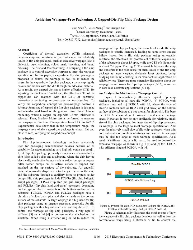
Figure 1 schematically illustrates typical flip chip
packages, including (a) bare die FCBGA, (b) FCBGA with
stiffener ring, and (c) FCBGA with lid, where the type of
electric contacts such as BGA (ball grid array) on the bottom
surface of the substrate are not shown for simplicity. The bare
die FCBGA is desired due to lower cost and smaller package
stress. However, it may be only applicable for relatively small
size of flip chip packages. For large size of flip chip packages,
its warpage is too large to meet warpage specification. And
even for relatively small size of flip chip packages, when thin
core substrates or coreless substrates are desired, its warpage
may be also too large to meet warpage specification. As a
result, a stiffener ring or a lid has to be used to control the
excessive warpage, as shown in Fig. 1 (b) and (c) for FCBGA
with stiffener ring and FCBGA with lid.
Figure 1. Typical flip chip BGA packages: (a) bare die FCBGA, (b)
FCBGA with stiffener ring, and (c) FCBGA with lid.
Figure 2 schematically illustrates the mechanisms of how
the warpage of a flip chip package develops as well as how the
conventional ways using a stiffener or lid to control the
978-1-4799-8609-5/15/$31.00 ©2015 IEEE 1546 2015 Electronic Components & Technology Conference
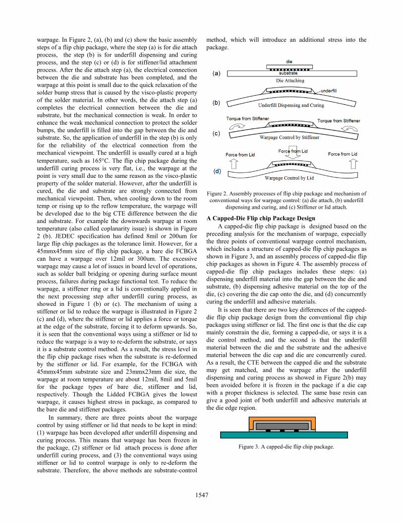
warpage. In Figure 2, (a), (b) and (c) show the basic assembly
steps of a flip chip package, where the step (a) is for die attach
process, the step (b) is for underfill dispensing and curing
process, and the step (c) or (d) is for stiffener/lid attachment
process. After the die attach step (a), the electrical connection
between the die and substrate has been completed, and the
warpage at this point is small due to the quick relaxation of the
solder bump stress that is caused by the visco-plastic property
of the solder material. In other words, the die attach step (a)
completes the electrical connection between the die and
substrate, but the mechanical connection is weak. In order to
enhance the weak mechanical connection to protect the solder
bumps, the underfill is filled into the gap between the die and
substrate. So, the application of underfill in the step (b) is only
for the reliability of the electrical connection from the
mechanical viewpoint. The underfill is usually cured at a high
temperature, such as 165C. The flip chip package during the
underfill curing process is very flat, i.e., the warpage at the
point is very small due to the same reason as the visco-plastic
property of the solder material. However, after the underfill is
cured, the die and substrate are strongly connected from
mechanical viewpoint. Then, when cooling down to the room
temp or rising up to the reflow temperature, the warpage will
be developed due to the big CTE difference between the die
and substrate. For example the downwards warpage at room
temperature (also called coplanarity issue) is shown in Figure
2 (b). JEDEC specification has defined 8mil or 200um for
large flip chip packages as the tolerance limit. However, for a
45mmx45mm size of flip chip package, a bare die FCBGA
can have a warpage over 12mil or 300um. The excessive
warpage may cause a lot of issues in board level of operations,
such as solder ball bridging or opening during surface mount
process, failures during package functional test. To reduce the
warpage, a stiffener ring or a lid is conventionally applied in
the next processing step after underfill curing process, as
showed in Figure 1 (b) or (c). The mechanism of using a
stiffener or lid to reduce the warpage is illustrated in Figure 2
(c) and (d), where the stiffener or lid applies a force or torque
at the edge of the substrate, forcing it to deform upwards. So,
it is seen that the conventional ways using a stiffener or lid to
reduce the warpage is a way to re-deform the substrate, or says
it is a substrate control method. As a result, the stress level in
the flip chip package rises when the substrate is re-deformed
by the stiffener or lid. For example, for the FCBGA with
45mmx45mm substrate size and 23mmx23mm die size, the
warpage at room temperature are about 12mil, 8mil and 5mil
for the package types of bare die, stiffener and lid,
respectively. Though the Lidded FCBGA gives the lowest
warpage, it causes highest stress in package, as compared to
the bare die and stiffener packages.
In summary, there are three points about the warpage
control by using stiffener or lid that needs to be kept in mind:
(1) warpage has been developed after underfill dispensing and
curing process. This means that warpage has been frozen in
the package, (2) stiffener or lid attach process is done after
underfill curing process, and (3) the conventional ways using
stiffener or lid to control warpage is only to re-deform the
substrate. Therefore, the above methods are substrate-control
method, which will introduce an additional stress into the
package.
Figure 2. Assembly processes of flip chip package and mechanism of
conventional ways for warpage control: (a) die attach, (b) underfill
dispensing and curing, and (c) Stiffener or lid attach.
A Capped-Die Flip chip Package Design
A capped-die flip chip package is designed based on the
preceding analysis for the mechanism of warpage, especially
the three points of conventional warpage control mechanism,
which includes a structure of capped-die flip chip packages as
shown in Figure 3, and an assembly process of capped-die flip
chip packages as shown in Figure 4. The assembly process of
capped-die flip chip packages includes these steps: (a)
dispensing underfill material into the gap between the die and
substrate, (b) dispensing adhesive material on the top of the
die, (c) covering the die cap onto the die, and (d) concurrently
curing the underfill and adhesive materials.
It is seen that there are two key differences of the capped-
die flip chip package design from the conventional flip chip
packages using stiffener or lid. The first one is that the die cap
mainly constrain the die, forming a capped-die, or says it is a
die control method, and the second is that the underfill
material between the die and the substrate and the adhesive
material between the die cap and die are concurrently cured.
As a result, the CTE between the capped die and the substrate
may get matched, and the warpage after the underfill
dispensing and curing process as showed in Figure 2(b) may
been avoided before it is frozen in the package if a die cap
with a proper thickness is selected. The same base resin can
give a good joint of both underfill and adhesive materials at
the die edge region.
Figure 3. A capped-die flip chip package.
1547

Figure 4. Assembly process for capped-die flip chip package.
Some potential failure modes of capped-die flip chip
packages are illustrated in Figure 5. The reason for the
possible failure modes is that a high stress may take place
around the die edge region when the die cap constrains the
deformation of the die during temperature change. Based on
this consideration, an improved die cap is designed to lessen
the risk of the failure modes. The capped-die flip chip
packages using an improved die cap is shown in Figure 6.
Figure 5. Potential failure modes for capped-die flip chip packages.
Figure 6. A capped-die flip chip package using an improved die cap
design.
It is suggested that the adhesive material should have the
same Tg as that of the underfill material so that both materials
consistently become softer or harder when temperature passes
Tg. It is preferred that both materials use the same resin as
their base materials, and their fillers may be different. For
example, for the thermal purpose, the fillers of the adhesive
material for bonging the die cap with the die may use high
conductive fillers, such as silver flakes.
Experimental Verification for Capped-Die Concept
The test vehicle for the experimental verification is a flip
chip package with 45mmx45mm substrate size, 23mmx23mm
die size and 0.78mm die thickness. Two package structures of
dare die and capped die are tested and compared, as shown in
Figure 7. The substrate of the flip chip package has eight
metal layers and 0.8mm thickness of core. The CTE and
Young’s modulus of the core are 11.3 ppm/C and 32GPa. In
the test, the same underfill material is used as the adhesive
material for bonding the die cap and the die. Two underfill
materials, U6 and U2 are selected. The Tg of U6 and U2 are
95C and 135C, respectively. The material of the die cap is
copper. FEM simulation is used to determine a proper
thickness of the die cap, which shows that 0.4mm thickness of
die cap may achieve a warpage-free flip chip package for the
test vehicle. For comparison, a 0.2mm thickness of die cap is
also tested. The test data by shadow moiré show that the
warpage control using 0.2mm thickness of die cap is only a
little better than that by a stiffener ring, and an ideal warpage
control is achieved by 0.4mm thickness of die cap, as
expected by FEM simulation. For bare die package and
capped die package with 0.4mm thickness of die cap, the test
data of warpage vs. temperature are shown in Figure 8. The
data are expected by FEM simulation which will be showed in
the following section together with more simulations for the
capped-die package design.
Figure 7. Photos of test vehicles for verifying the capped-die
concept: (a) bare die package structure, (b) capped-die package
structure.
Figure 8. Shadow Moiré data for bare die and capped-die flip chip
packages, where the symbol 6B and 2B stand for bare die package
structure using underfill material U6 and U2, and 6C and 2C stand
for Capped-die package structure using underfill material U6 and
U2.
Some interesting features observed from the test data of
capped-die flip chip package are discussed as follows. One
feature is that when temperature changes, the capped-die
package does not warp up and down, or the warpage curve is
almost flat and at a warpage value of about 65um. The feature
of no warping up and down means high board-level reliability
when mounting the package on a board and under thermal
cycling loading. Also, this feature means that the stress
variation inside the package during thermal cycling loading
under component level is low, giving high component level
reliability. Another feature is that the warpage of the capped-
die flip chip packages is independent of underfill Tg, which is
different from conventional flip chip package where higher Tg
of underfill causes higher warpage at room temperature. It is
known that there are two issues for conventional flip chip
package to use very high Tg of underfill material. One is
higher warpage and the other is higher stress at die corner.
The two issues may be avoided by using capped-doe flip chip
packages. So, for capped-die flip chip package, underfill
materials with higher Tg than 120C may be applicable. As a
result, the underfill material will not become soft from hard
1548

under application or test loading conditions, improving the
reliability of bumps and low-k layers of the package.
Finally, it is explained why the capped-die package gets
stable at the small warpage value 65um. In fact, the warpage
value is the warpage of the flip chip package at curing
temperature 165C. It is seen from Figure 8 that the bare die
package is just having the warpage value around the
temperature. The warpage value of the capped die package no
longer varies with temperature because the CTE of capped die
and substrate gets matched. Two factors may cause the small
warpage value. One is the residual stress from solder bumps,
and the other is the initial warpage of bare substrate due to
unsymmetrical metal layers above and below the core. It is not
necessary to eliminate the small warpage. For finite element
modeling (FEM), one usually assumes that the package is flat
at curing temperature of underfill material.
In conclusion, capped die concept may give a promising
package structure with the advantages of warpage-free control
and low stress or high reliability in component as well as
board levels. In the following section, FEM simulation is
performed for a preliminary investigation for capped die
package design.
FEM Analysis for Capped-Die Flip chip Package Design
Numerical simulation is a quick and efficient way for
sensitivity study. FEM software ANSYS is utilized to carry
out the numerical simulation.
(1) Comparison with experimental data
The same flip chip package used in the preceding test
vehicle is used as an example for FEM simulation. The stress-
free temperature is assumed as curing temperature 165C.
Four package structures are compared, including bare die,
stiffener, lid and capped-die packages. The stiffener
dimension is 0.6mm thick and 7mm wide, the lid dimension is
1.5mm thick and 4mm foot width, and the die cap is 0.4mm
thick. The simulation results for the contour plot of the
deformation of the four packages at room temperature are
shown in Figure 9, where W25C stands for the warpage at room
temperature which is defined as the difference between the
substrate bottom center and the lowest point. It is seen from
Figure 9 that the capped-die package gives an ideal warpage
control. Note that the simulation result shown in Figurer 9(a)
for the room temperature warpage of the bare die package is
agreeable with the test data showed in Figure 8, validating the
FEM model.
Figure 9. FEM results of warpage for comparing various package
structures.
(2) Achieving warpage-free packaging:
The major dimension for a die cap is its thickness. The
size of a die cap follows the size of the corresponding die,
being a little bigger than the die. It is suggested that the gap
between the die edge and the side of the die cap is in the range
of 100um to 300um. The smaller the gap is the stronger
constraints that the die cap applies to the die, but the higher
risk the failure between the die and the die cap. A proper gap
size needs to be determined by experimental test for each case.
In the FEM simulation, a proper thickness is determined for
different size of flip chip packages, including a big size, a
medium size and a small size of packages. Besides the room
temperature warpage, the high temperature warpage is also
important and needs to be controlled. The FEM simulation is
used to check if both warpage can be controlled in the same
time.
The big package is the same as the test vehicle, i.e.,
substrate size is 45mmx45mm, die size and thickness are
23mmx23mm and 0.78mm. The substrate has eight metal
layers and 0.8mm thickness of core. The CTE and Young’s
modulus of the core are 11.3 ppm/C and 32GPa. For the
medium size of package, its substrate size is 30mmx30mm,
die size and thickness are 17mmx17mm and 0.3mm. And For
the small size of package, its substrate size is 20mmx20mm,
die size and thickness are 10mmx10mm and 0.1mm. The
substrate of the medium size of package has six metal layers
and 0.4mm thickness of core. The substrate of the small size
of package has six metal layers and 0.15mm thickness of core.
The core materials of the medium and small packages are the
same as the big package.
The die cap thicknesses are 0.4mm, 0.3mm and 0.25mm
for the three packages, respectively. The simulation results of
the contour plot of the deformation of the packages at room
and high temperatures are showed in Figures 10A, 10B and
10C, where W25C and W260C stand for the warpage at 25C and
260C, respectively. It is seen that a warpage-free packaging
for the different size of packages are theoretically achieved by
a proper thickness of die cap. In practice, it is difficult to
achieve so small warpage because there is an initial warpage
when curing the underfill material. It is ideal to achieve a flat
warpage curve vs. temperature, as shown by the test data in
Figure. 8.
1549

Figure 10A. Contour plot of the deformation of the big size of
package at room and high temperatures.
Figure 10B. Contour plot of the deformation of the medium size of
package at room and high temperatures.
Figure 10C. Contour plot of the deformation of the small size of
package at room and high temperatures.
(3) Effect of the thickness of die cap
In the preceding section for achieving warpage-free
packaging, the die cap thickness is selected by trial and error
method through multiple rounds of simulations. Here, an
interesting phenomenon, called over-controlled warpage is
shown about warpage-control by capped-die when a thicker
die cap is selected. In the simulation example, the same big
package is used, but a thinner substrate core, 0.4mm thickness
of core is considered. It has been seen that for 0.8mm
thickness of core, 0.4mm thickness of die cap gives an ideal
warpage control. The simulation shows a phenomenon of
over-controlled warpage by the same 0.4mm thickness of die
cap for the package with the thinner core, as shown in Figure
11(b). For the thin core, a thinner die cap, i.e., a 0.3mm
thickness of die cap is proper for an ideal warpage control, as
shown in Figure 11(c). Note that the conventional stiffener
and lid for warpage control never give the phenomenon of
over-controlled warpage even though a very thick stiffener or
lid is used.
Figure 11, FEM results for proper die cap thickness vs. substrate
core thickness.
(4) Warpage-free Control for Coreless Substrate
Compared to substrates with core, coreless substrates can
shrink substrate size as well as improve the functional
performance of flip chip packages. So, it is desired for
packaging application. However, flip chip packages using
coreless substrates have very excessive warpage due to the
low rigidity of coreless substrates. And it is not easy to control
the high warpage using a stiffener or lid for big package size.
It is known that coreless substrates exhibit a severe W-shape
when its substrate warpage is controlled by stiffener or lid,
limiting its extensive application.
FEM simulation is used to investigate the effect of capped
die method for controlling the warpage of packages using
coreless substrates. Two package sizes are simulated: a big
package and a small package. Their dimensions and substrate
metal layers are the same as the big and small packages done
in the preceding section except the substrate type. For a
comparison, bare die packages are also simulated. Simulation
results are shown in Figures 12 and 13 for the big and small
flip chip packages, respectively. It is seen that the huge room
temperature warpage is ideally controlled by a 0.25mm
thickness of die cap. One interesting thing is that for both bid
and small packages, the warpage-free control happens to be
achieved by the same thickness of die cap. Note that the
substrate has eight metal layers and die thickness is 0.78mm in
the big package (45mmx45mm), and the substrate has six
metal layers and die thickness is 0.1mm in the small package
(10mmx10mm).
1550

Figure 12. Contour plot of the deformation of big package using 8
layers of coreless substrate at room temperatures.
Figure 13. Contour plot of the deformation of small package using 6
layers of coreless substrate at room temperatures.
Conclusions
The experimental and simulation results show that
warpage-free packaging in the full range of temperature
variation can be achieved by using capped-die flip chip
package design. More experimental studies about the capped-
die flip chip package design are needed, especially for its
possible failure modes. Some major design considerations
include the selection of adhesive material for bonding the die
cap with the die, a proper thickness of die cap, and a proper
gap between the die cap side and the die edge. The assembly
process needs to be carefully performed to avoid the voids
between the die cap and the die because both adhesive and
underfill materials are concurrently cured. About the selection
of adhesive material, it is suggested to use one which has the
same resin as that of underfill material, but contains high
thermal conductive fillers, like silver flakes. As a result, both
adhesive and underfill materials can have a good combination
at the die edge region, improving the reliability between the
die cap and die, and in the meantime, the thermal performance
of the capped-die package can be good enough for high power
application.
Acknowledgments
Authors would like to thank SPIL (Siliconware Precision
Industries Co., Ltd) for their contributions to this project.
References
[1] X.J. Fan, H. Wang and T. Lim, "Investigation of the
underfill delamination and cracking in flip-chip
modules under temperature cyclic loading," IEEE
Transactions on Components and Packaging
Technologies, vol. 24, pp. 84-91, 2001.
[2] G.Q. Zhang, W.D. van Driel and X.J. Fan,
Mechanics of microelectronics vol. 141: Springer
Science & Business Media, 2006.
[3] X. Liu, M. Li, D.R. Mullen, J. Cline and S.K.
Sitaraman, "Experimental and Simulation Study of
Double-Sided Flip-Chip Assembly With a Stiffener
Ring," IEEE Transactions on Device and Materials
Reliability, vol. 14, pp. 512-522, 2014.
[4] P. Sun, V. Zhang, R. Xu and T. Zhang, "Underfill
selection for large body (50× 50mm) lidded flip chip
BGA package with ELK 40nm Pb-free bumps," in
2012 13th International Conference on Electronic
Packaging Technology and High Density Packaging
(ICEPT-HDP), 2012, pp. 1650-1654.
[5] D. Campos, R. Pilard, E. Saugier, Y. Imbs, J.-M.
Riviere, J. Lopez, P. Calascibetta, N. Chevrier, L.
Petit and N. Martin, "60GHz BGA solution
packaging reliability and warpage study," in 2013
European Microelectronics Packaging Conference
(EMPC), 2013, pp. 1-4.
[6] R.L. Hubbard and P. Zappella, "Low warpage flip-
chip under-fill curing," IEEE Transactions on
Components, Packaging and Manufacturing
Technology, vol. 1, pp. 1957-1964, 2011.
[7] K.M. Jansen and B. Ozturk, "Warpage Estimation of
a Multilayer Package Including Cure Shrinkage
Effects," IEEE Transactions on Components,
Packaging and Manufacturing Technology, vol. 3,
pp. 459-466, 2013.
[8] W. Lin, B. Baloglu and K. Stratton, "Coreless
substrate with asymmetric design to improve package
warpage," in 2014 IEEE 64th Electronic Components
and Technology Conference (ECTC), 2014, pp.
1401-1406.
[9] W. Lin, S. Wen, A. Yoshida and J. Shin, "Evaluation
of raw substrate variation from different suppliers
and processes and their impact on package warpage,"
in 2012 IEEE 62nd Electronic Components and
Technology Conference (ECTC), 2012, pp. 1406-
1411.
[10] A.-H. Liu, D.W. Wang, H.-M. Huang, M. Sun, M.-R.
Lin, C. Zhong, S.-J. Hwang and H.-H. Lu,
"Characterization of fine-pitch solder bump joint and
package warpage for low K high-pin-count flip-chip
BGA through Shadow Moiré and Micro Moiré
techniques," in 2011 IEEE 61st Electronic
Components and Technology Conference (ECTC),
2011, pp. 431-440.
[11] T.H. Wang, C.-I. Tsai, C.-C. Lee and Y.-S. Lai,
"Study of factors affecting warpage of HFCBGA
subjected to reflow soldering-liked profile,"
Microelectronics Reliability, vol. 53, pp. 297-302,
2013.
[12] D.G. Yang, K.M.B. Jansen, L.J. Ernst, G.Q. Zhang,
W.D. van Driel, H.J.L. Bressers and X.J. Fan,
"Prediction of process-induced warpage of IC
packages encapsulated with thermosetting polymers,"
1551
in Proceedings of 54th Electronic Components and
Technology Conference, 2004, 2004, pp. 98-105.
[13] X.J. Fan, J. Zhou and G.Q. Zhang, "Multi-physics
modeling in virtual prototyping of electronic
packages–combined thermal, thermo-mechanical and
vapor pressure modeling," Microelectronics
Reliability, vol. 44, pp. 1967-1976, 2004.
[14] K. Sakuma, E. Blackshear, K. Tunga, C. Lian, S. Li,
M. Interrante, O. Mantilla and J.-W. Nah, "Flip chip
assembly method employing differential
heating/cooling for large dies with coreless
substrates," in 2013 IEEE 63rd Electronic
Components and Technology Conference (ECTC),
2013, pp. 667-673.
1552