accurate opto-electrical modeling of multi-crystalline silicon wafer-based solar cells
TRANSCRIPT

Accurate opto-electrical modeling of multi-crystalline siliconwafer-based solar cells
Andrea Ingenito n, Olindo Isabella, Serge Solntsev, Miro ZemanDelft University of Technology, PVMD/Dimes, Mekelweg 4, 2628 CD Delft, the Netherlands
a r t i c l e i n f o
Article history:Received 7 May 2013Received in revised form23 October 2013Accepted 13 December 2013Available online 21 January 2014
Keywords:Opto-electical modelingMulti-crystalline siliconWafer-based solar cells
a b s t r a c t
Modeling of multi-crystalline silicon solar cells has been recently widely used for fast and cost-effectiveperformance improvements. The optimization of device performance requires deep understanding of theopto-electrical losses in a fabricated solar cell. To carry out trustworthy simulations for performanceanalysis and optimization, the simulation program has to be calibrated to the performance of thefabricated device. In this article an accurate opto-electrical modeling of multi-crystalline silicon solarcells is presented. Specific issues that arose during the calibration process were addressed, such as theoptical model describing light scattering due to wafer texturing, the electrical modeling of heavily dopedemitter and the opto-electrical modeling of the back surface field. Calibrated model parameters, obtainedfrom theory or measurements, led to an excellent simultaneous matching between simulated andmeasured reflectance spectrum, internal and external quantum efficiencies and dark and illuminatedcurrent–voltage characteristics of the multi-crystalline silicon solar cells. In addition, opto-electricallosses in the investigated solar cells were determined and quantified.
& 2014 Elsevier B.V. All rights reserved.
1. Introduction
The structure of highly efficient solar cells based on crystallinesilicon (c-Si) is a complex opto-electrical system. To enhance theabsorption in the bulk region of the silicon wafer and thusincreasing the short-circuit current density (JSC), several lightmanagement techniques are employed at the same time. Anti-reflective coatings, surface textures for light scattering at both thefront and rear side and efficient back reflectors can be typicallyfound in nowadays0 solar cells. In addition, to improve thecollection of photo-generated carriers and thus increasing theopen circuit voltage (VOC) and the fill factor (FF), the bulk regionis sandwiched between the (selective) emitter at the front side andthe back surface field (BSF) region at the rear side combined withfront and back passivation layers [1]. Hence, for integrated analysisand optimization of the opto-electrical performance of this complexdevice, computer modeling has become an extremely importanttool [2]. Due to doping concentration profiles in the emitter and BSFthat vary over many orders of magnitude in thin regions the computermodel must use Fermi-Dirac statistics in order to properly describe thebehavior of such degenerate layers [3].
In this work we present (i) a detailed opto-electrical modelbased on the Advanced Semiconductor Analysis (ASA) program [4]
of an industrial multi-crystalline silicon (mc-Si) solar cell that wasused as a reference and (ii) the analysis of opto-electrical losses ofthese devices. Special care was devoted to the assignment ofproper values to the input parameters of the numerical model.This step is known as calibration of model parameters [5–7].Generally a calibration process consists of tuning a number ofinput parameters until a good matching between measured andsimulated characteristics of the reference solar cell is achieved.Despite the simplicity of this approach, it must be noted that theextracted values of input parameters might not be unique orrepresent realistic values. To avoid this situation, we used asstarting values those predicted by theory or experimentallydetermined. In particular, for proper modeling of anti-reflectiveeffect and light trapping in mc-Si solar cells, the morphologicalanalysis together with the measurements of optical properties ofthe device were carried out. In order to realistically represent thefront emitter, the mechanisms of electrical recombination wereinvestigated and the values of fitting parameters such as surfacevelocity recombination (SVR) and minority carrier lifetime werecompared with those predicted by the theory. In case of the bulksilicon, the electrical recombination in the bulk and at the rear sideof the solar cell was described by using the effective minoritycarrier diffusion length extracted from the measured internalquantum efficiency (IQE) of the reference device. Finally, focusingon the rear side, the back reflectance was described with opticalproperties of Si–Al alloy and scattering parameters, while
Contents lists available at ScienceDirect
journal homepage: www.elsevier.com/locate/solmat
Solar Energy Materials & Solar Cells
0927-0248/$ - see front matter & 2014 Elsevier B.V. All rights reserved.http://dx.doi.org/10.1016/j.solmat.2013.12.019
n Corresponding author.Tel.:+31 0 1527 88905, fax:+31 0 15 27 82968.E-mail address: [email protected] (A. Ingenito).
Solar Energy Materials & Solar Cells 123 (2014) 17–29
recombination losses were also modeled in terms of the effectiveminority carrier diffusion length.
Using the parameters of our calibrated opto-electrical model,the simulated reflectance spectrum (R), the internal and externalquantum efficiencies (EQE) and (iii) the dark and illuminatedcurrent–voltage characteristics (J–V) characteristic simultaneouslymatched very well the measured curves of a commercial referencemc-Si solar cell. Furthermore, the opto-electrical losses in allsupporting layers of the reference solar cell were determinedand quantified. Our calibrated model can be applied to simulate allc-Si based solar cells.
2. Overview of the opto-electrical device simulators for C–Sisolar cells
Numerical modeling has been widely applied to c-Si solar cellsboth by academic institutions and industry. Commercially avail-able software programs like ATLAS [8], SENTAURUS [9,10], andMICROTECH [11] are the most common software programs used bythe photovoltaic (PV) industry. However, specific physical modelsmay be absent in these commercial software programs or have tobe adapted. For these reasons, many research groups have devel-oped their own advanced physical models describing processes insolar cells that are not implemented yet in commercial computerprograms.
For simulating the electrical operation of c-Si wafer-based solarcells, it is sufficient to solve the two-carrier time-dependentsemiconductor transport equations in one dimension. In 1960s,Gummel from Bell Laboratories introduced an iterative method tosolve this set of equations [12]. Since then, several models based onhis numerical approach were developed and applied to Si wafer-based solar cells. Around 10 years later, a numerical code waswritten and used at Bell Laboratories to investigate and designsolar cells with conversion efficiency higher than 20% [13,14].In 1980s, the SCAP1D software was developed at Purdue University.This software programwas later extended into two dimensions andenabled to simulate a broad variety of solar cell structures such asinterdigitated back contact solar cells [15,16]. In mid-1980s, a one-dimensional (1-D) semiconductor simulator called PC-1D [17] wasdeveloped as free-available software. In contrast with most of thedevice simulators at the time, it solved the equations not using thefinite difference method but the finite element method. This soft-ware, broadly used by the PV community, has strongly contributedto the progress in design of highly efficient c-Si solar cells [18,19].Recently, the PC-1D software has been used together with theoptical modeling of the so-called isotexture [20] to simulate theopto-electrical behavior of mc-Si solar cells [21].
The AFORSHET software, developed at Helmholtz Centre inBerlin, has been mainly used for simulating hetero-junctionsilicon-based solar cells [22]. The DESSIS software was used atUniversity of New South Wales in Sydney to analyze c-Si solarcells. Simulation results were employed to realize a solar cell witha record efficiency of 24.7% in 1994 [23–25] and to optimize thedesign of a solar cell on a 47 μm thick float-zone c-Si wafer withrecord efficiency of 21.5% [26]. In 2011 the PV Lighthouse websitewas launched. The web site offers online free calculators thatsimulate various aspects of solar cell operation [27].
The abovementioned software programs are mainly suited foranalysis and optimization of the electrical performance of solarcells. The trend in PV industry towards the use of fewer rawmaterials demands the development and application of advancedlight management techniques in order to maximize light absorptionin thinner c-Si wafers. This trend also requires that modeling cancorrectly handle optical processes such as scattering, diffraction andplasmonic absorption using textured surfaces in c-Si solar cells.
Since typical c-Si solar cells accommodate textures whose featuresare much larger than the incident wavelengths, ray tracingapproach is widely employed to calculate the optical properties ofc-Si solar cells. The most frequent models rayn [28], texture [29],sunrays [30], raysim [31], sonne [32] and recently introduceddaidalos [33] or crowm [34] are three dimensional (3-D).To incorporate optical results of 3-D models into a 1-D devicesimulator, the 3-D generation profile G(x,y,z) is usually averagedin a 1-D generation profile G(z) which describes the opticalsituation inside the device along its depth [7]. Recently, better lightin-coupling and light scattering triggered by textures with smaller-than-wavelength features are being implemented also in c-Siwafer solar cells [35]. In this case, both coherent non-scattered(i.e. specular) and incoherent scattered (i.e. diffused) light inside thedevice must be considered [36]. Examples of optical simulators thattake into account both specular and scattered light propagation areoptical models from École Polytechnique Palaiseau [37], sunshineprogram from Ljubljana University [38], GENPRO3 optical moduleimplemented in the ASA program of Delft University of Technology[39] and the Prague optical model [40].
The ASA program was developed and used at Delft University ofTechnology to simulate thin-film amorphous Si solar cells. For thispurpose advanced models for describing the properties of the amor-phous silicon were implemented in this program. Later the ASAprogram was extended with the models that enabled the programto simulate c-Si solar cells. In this contribution we demonstrate thatthe optical and electronic models that are implemented in the ASAprogram can be used for simulating state-of-the-art mc-Si solar cellsfabricated with industrial-scale processes.
2.1. The ASA device simulator
The ASA program is a 1-D device simulator that integrates bothoptical and electrical simulations for the complete modeling ofsolar cell operation. From optical point of view, solar cells aremulti-layered optical systems with flat and/or textured interfaces.Since all practical c-Si solar cells use textured surfaces, modelingmust take into account refraction and scattering at these surfacesin order to calculate the absorption profile accurately. In case ofscattering, an optical model has to take into account both coherentand incoherent light propagation throughout the simulated device[38]. The optical model GENPRO3 implemented in the ASAprogram fulfils this requirement and, in addition to wavelength-dependent complex refractive indices of individual layers, uses asinput descriptive scattering parameters of a rough interface, likehaze and angular intensity distribution (AID) [41]. Simulatinga solar cell with the ASA program, optical outputs are theR spectrum, the absorptance spectrum (A) in each layer of themulti-layered structure and the generation rate related to theoptical absorption profile. Once the generation rate is determined,it is used as an input for the electrical simulations.
The electrical part of the ASA device simulator is based onsemiconductor equations and includes, among other models,Shockley–Read–Hall (SRH) and Auger recombination-generationrates as well as the Fermi–Dirac statistics. Particularly, the depen-dence of carriers mobility, diffusion lengths, band-gap narrowingand minority-carrier lifetime on the doping densities of donors(ND) and acceptors (NA) is included. The steady state operation ofhomo-junction semiconductor device is described by a set ofcoupled differential equations which, in general, cannot be solvedanalytically. In the ASA program, this set of equations is solved bymeans of numerical methods. The free electron concentration, n,the hole concentration, p, and the electrostatic potential, ψ, areused as variables. After reading structure-statements from aninput file, the ASA engine (i) generates a grid along the depth ofthe device, (ii) carries out the spectral absorption rate and the
A. Ingenito et al. / Solar Energy Materials & Solar Cells 123 (2014) 17–2918
reflectance / transmittance spectra, (iii) solves the Poisson equa-tion at thermal equilibrium and finally (iv) computes the currentdensity–voltage characteristic with Newton–Raphson [42] and/orGummel [12] methods. Once the set of equations has been solved,quantities such as energy band diagram, electron–hole concentra-tion and electric field profile can be also carried out. Finally,external parameters of the device performance such as spectralresponse, dark and illuminated current–voltage characteristics arecalculated. The equivalent circuit to model the J–V characteristicscan be chosen between the basic one-diode model and the moreadvanced two-diodes model [43].
3. Structure and characterization of the reference Mc-Sisolar cell
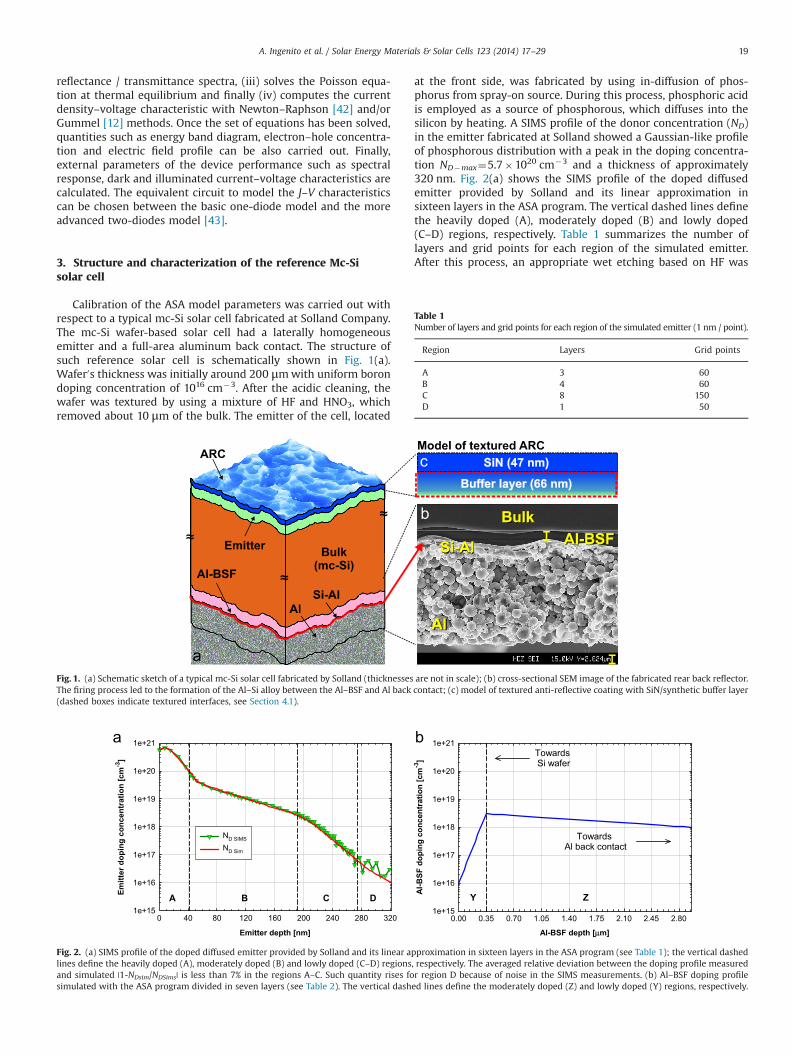
Calibration of the ASA model parameters was carried out withrespect to a typical mc-Si solar cell fabricated at Solland Company.The mc-Si wafer-based solar cell had a laterally homogeneousemitter and a full-area aluminum back contact. The structure ofsuch reference solar cell is schematically shown in Fig. 1(a).Wafer0s thickness was initially around 200 μmwith uniform borondoping concentration of 1016 cm�3. After the acidic cleaning, thewafer was textured by using a mixture of HF and HNO3, whichremoved about 10 μm of the bulk. The emitter of the cell, located
at the front side, was fabricated by using in-diffusion of phos-phorus from spray-on source. During this process, phosphoric acidis employed as a source of phosphorous, which diffuses into thesilicon by heating. A SIMS profile of the donor concentration (ND)in the emitter fabricated at Solland showed a Gaussian-like profileof phosphorous distribution with a peak in the doping concentra-tion ND�max¼5.7�1020 cm�3 and a thickness of approximately320 nm. Fig. 2(a) shows the SIMS profile of the doped diffusedemitter provided by Solland and its linear approximation insixteen layers in the ASA program. The vertical dashed lines definethe heavily doped (A), moderately doped (B) and lowly doped(C–D) regions, respectively. Table 1 summarizes the number oflayers and grid points for each region of the simulated emitter.After this process, an appropriate wet etching based on HF was
Fig. 1. (a) Schematic sketch of a typical mc-Si solar cell fabricated by Solland (thicknesses are not in scale); (b) cross-sectional SEM image of the fabricated rear back reflector.The firing process led to the formation of the Al–Si alloy between the Al–BSF and Al back contact; (c) model of textured anti-reflective coating with SiN/synthetic buffer layer(dashed boxes indicate textured interfaces, see Section 4.1).
Emitter depth [nm]
Emitt
er d
opin
g co
ncen
trat
ion
[cm
-3]
1e+15
1e+16
1e+17
1e+18
1e+19
1e+20
1e+21
A B C D
Al-BSF depth [μm]
0 40 80 120 160 200 240 280 320 0.00 0.35 0.70 1.05 1.40 1.75 2.10 2.45 2.80
Al-B
SF d
opin
g co
ncen
trat
ion
[cm
-3]
1e+15
1e+16
1e+17
1e+18
1e+19
1e+20
1e+21
Towards Al back contact
Towards Si wafer
ZY
NN
Fig. 2. (a) SIMS profile of the doped diffused emitter provided by Solland and its linear approximation in sixteen layers in the ASA program (see Table 1); the vertical dashedlines define the heavily doped (A), moderately doped (B) and lowly doped (C–D) regions, respectively. The averaged relative deviation between the doping profile measuredand simulated |1-NDsim/NDSims| is less than 7% in the regions A–C. Such quantity rises for region D because of noise in the SIMS measurements. (b) Al–BSF doping profilesimulated with the ASA program divided in seven layers (see Table 2). The vertical dashed lines define the moderately doped (Z) and lowly doped (Y) regions, respectively.
Table 1Number of layers and grid points for each region of the simulated emitter (1 nm / point).
Region Layers Grid points
A 3 60B 4 60C 8 150D 1 50
A. Ingenito et al. / Solar Energy Materials & Solar Cells 123 (2014) 17–29 19

used to remove the residual of phosphosilicate glass. A SiN layerwas deposited by PECVD on top of the emitter. It served as frontside passivation of solar cell as well as anti-reflective coating(ARC). Its thickness of 80 nm was designed for minimizing thereflectance at wavelengths around 650 nm.
For the formation of front and back contacts, a typical industrialprocess involving screen-printing and co-firing was used. During theco-firing, the silver metal grid printed on the front surface penetratesthrough the antireflection coating making contact with underlyingsilicon, while full-area Al–BSF forms at the rear side. In particular, thefiring process at the back side leads to the formation of a p7Si / Si–Al eutectic/agglomerated Al back contact [44]. The p7type Si layerset up the BSF and had a doping concentration between 1017 to1018 cm�3 within a thickness of around 3 μm. The agglomerated Alscreen printed layer was around 30 μm thick. The real doping profileof the reference cell could not be provided by the company forconfidential reasons. Therefore, we used the typical doping profilemeasured for standard Al–BSF [45] (see Fig. 2(b)). The vertical dashedlines in Fig. 2(b) define the moderately doped (Z) and lowly doped(Y) regions respectively. Table 2 summarizes the number of layersand grid points used for each region of the simulated Al-BSF. A cross-sectional scanning electron microscopy (SEM) image of the backcontact in the fabricated reference cell is reported in Fig. 1(b). Anoverview of layers thickness related to the reference solar cell ispresented in Table 3.
The characterization of such reference mc-Si solar cell was carriedout at Solland, where dark and illuminated J–V characteristics, seriesand shunt resistance, IQE, EQE and total reflectance R were measured.Further morphological and optical characterizations were carried outat Delft University of Technology. Atomic force microscopy (AFM)image of wafer0s textured surface is presented in Fig. 3, where large
random features with peak-to-peak height larger than 4 μm arerecognizable. In addition, the average inclination angle of surfacefacets was found to be 401. The scattering parameters of the cell werecharacterized with an Automated Reflectance/Transmittance Analyzer(ARTA) and integrating sphere (IS), accessories of a PerkinElmerLambda 950 spectro-photometer [46]. Diffuse and total componentsof reflected and transmitted light where measured and their ratios(haze parameters H) were calculated. Noteworthy, both HR and HT
were almost equal to one in the whole wavelength range of interest.This means that light in both reflectance and transmittance is fullydiffused by wafer0s surface. Fig. 4 demonstrates that the specularcomponent is almost absent in the AID since wafer0s surface acts as aLambertian scatterer at interface air/Si interface.
Also at Delft University of Technology, a phosphorus doped emitterwas fabricated on flat Float Zone wafers using POCl3 diffusion processin order to replicate the doping profile of Solland emitter. Opticalproperties of such heavily doped layer were determined withJ. A. Wollam Co. spectroscopic ellipsometer. Fig. 5 compares n and kfor standard un-doped Si with our measurements of the fabricatedemitter. The figure clearly shows that in case of high dopingconcentrations, the peaks at 350 nm and 370 nm of n andk spectra, respectively, are smoother than in case of un-dopedSi material. A similar behavior of the complex refractive index in caseof heavily doped Si is reported in reference [47].
Table 2Number of layers and grid points for each region of thesimulated Al-BSF (13 nm/ point).
Region Layers Grid points
Y 5 150Z 2 80
Table 3Layer thickness of the reference mc-Si solar cell.
Layer Thickness
SiN 80 nmEmitter (n-doped) 322 nmBulk mc-Si layer (NAE1016 cm�3) 190 μmBSF (p-doped) 2.95 μmSi–Al �1 μmAl 30 μm
Fig. 3. AFM scan of mc-Si wafer textured surface.
0.0001
0.001
0.01
0.1
30 40 50 60 70 80 90 100350
450
550
650
750
850
AID
R [-
]
Scattering angle [deg]
Wav
elen
gth
[nm
]
Fig. 4. AID in reflectance (AIDR) of the mc-Si etched surface in reflection at interfaceair/Si measured with the ARTA accessory.
Wavelength [nm]300 400 500 600 700 800
n [-]
0
1
2
3
4
5
6
7
k [-]
0
1
2
3
4
5
6
7
n undoped Si (JAW)k undoped Si (JAW)n doped Si k doped Si
Fig. 5. Real and imaginary part of the complex refractive index measured forun-doped and heavily doped silicon.
A. Ingenito et al. / Solar Energy Materials & Solar Cells 123 (2014) 17–2920

4. Calibration procedure
4.1. Optical modeling of front texture and anti-reflective coating
The surface texture of the wafer serves to scatter light into thesolar cell but also to introduce an anti-reflective effect. Suchcombined effect can be simulated either by ray tracing (seeSection 2) or by decoupling the anti-reflection from the scatteringwith appropriate optical models. We opted for this second choiceas compatible with the optical capabilities of the ASA program.
The optical model called GENPRO3 implemented in ASA wasused to simulate the light scattering. This model required as inputparameter the measured Haze and AID as function of the wave-length and scattering angle.
Unfortunately, the measured AIDR presented in Fig. 4 gives onlyindication about light scattering in reflectance at air/Si interface.To describe also the light scattering in transmittance we used theoptical model of isotextures, for which light scattered from acidictexturing shows a cos(3/2θ) distribution rather than Lambertian[20]. Here θ is the angle at which a ray traverses the substrate withrespect to the surface normal (scattering angle). Therefore, weinput in the ASA program the measured AIDR to describe thescattering in ASA by the front texturing in reflectance (see Fig. 4).This distribution was multiplied with cos(3/2θ) an input in ASAprogram as AIDT in order to describe the light scattering intransmittance (see Fig. 7).
The anti-reflective effect, due to random features of the surfacetexture and enhanced by the presence of SiN in the role of ARC,was simulated by adding an additional buffer layer on the top ofthe SiN layer, whose purpose was to decrease the total reflectanceby improving the light in-coupling at the front interface. Assketched in Fig. 1(c), we modeled such buffer layer by using asynthetic non-absorbing layer with a refractive index averagedbetween those of air and SiN. Varying the thickness of both bufferand SiN layers, a good matching between the measured andsimulated total reflectance was achieved until around 900 nm(dSiN¼47 nm and dbuffer¼63 nm, see Fig. 6). At wavelengths closeto the band gap edge of silicon, measured total reflectance can beinterpreted as back reflectance. In Section 4.5, where the rear sideof the device will be opto-electrically modeled, we shall properlyextend the modeling of total reflectance.
4.2. Electrical modeling of emitter/ARC interface passivation
The second step of our calibration focused on the electricalmodeling of front side passivation of solar cell emitter, since SiNARC layer reduces the surface recombination rate of excess carriers
[48]. According to the model presented by Steingrube et al. [49],under the assumption of low injection in the emitter, the effectivefront surface recombination velocity (FSRV) for flat n-type siliconcan be expressed as follows:
Sneff � flat ¼ Snc
Q2f
NDð0Þ ð1Þ
where Sn is the surface recombination velocity of un-passivatedn-type silicon; the constant c¼2εε0/qβ contains the dielectricpermittivity in vacuo (ε0), the relative permittivity of silicon (ε)and the elementary charge (q); β¼q/(KT) contains the Boltzmannconstant (K) and the absolute temperature (T); Qf
2 is the squaredvalue of positive fixed charges density ( Qf ¼ 2� 1012 C=cm2) inSiN layer [50], and ND(0)END�max is the emitter doping concen-tration at the Si/SiN interface (z¼0). Sn is function of dopingconcentration according to the following empirical equation [49]:
Sn ¼ Sref þα 1� ND� max
Nref
� �γ� �ð2Þ
where Sref¼4.37�103 cm/s, α¼3.6�103, Nref¼1014 cm�3 andγ¼�0.18 are determined experimentally in ref. [48]. Accordingto Eq. (1), Sneff�flat increases dramatically by augmenting thedoping concentration at Si/SiN interface. For our reference device,which had surface doping concentration Ndop�max¼5.7�1020 cm�3 and assuming the aforementioned density of fixedcharges Qf, the calculated Sneff�flat is equal to 1.68�105 cm/s.The modeling proposed is valid in case of polished wafers. Fortextured solar cells, Sneff�flat is worsened due to an increase in thesurface area. The effective FSRV that includes also this effect isdefined in [51] as:
Sneff ¼ Sneff � flatAT
AProj
� �ð3Þ
where AT and AProj are the textured and projected flat projectedarea, respectively. From AFM scan we measured AT/AProj¼1.22.Therefore, according to Eq. (3) and using data from our referencecell, theoretical Sneff is 2.05�105 cm/s. Referring to the results ofour calibration (see Section 5) for which a good agreement wasfound between measured and simulated solar cell external para-meters, a Sneff¼1.3�105 cm/s was extracted. The differencebetween theoretical and extracted value may be attributed to adifferent value of the fixed charge density for the deposited SiN.
Wavelength [nm]400 500 600 700 800 900 1000
R [-
]
0.0
0.2
0.4
0.6
0.8
1.0
80 nm SiN (simulated)47 nm SiN + 66 nm buffer (simulated)80 nm SiN (measured)
Fig. 6. Measured total reflectance of mc-Si reference solar cell. The antireflectiveeffect was simulated by combining SiN layer with an additional buffer layer.
0.0001
0.001
0.01
0.1
3040
5060
350
450
550
650750
850
AID
T [-]
Scattering angle [deg]
Wav
elen
gth
[nm
]
Fig. 7. AID in transmittance (AIDT) in the bulk silicon from the front texturingcalculated by multiplying the measured AIDR with cos(3/2θ).
A. Ingenito et al. / Solar Energy Materials & Solar Cells 123 (2014) 17–29 21
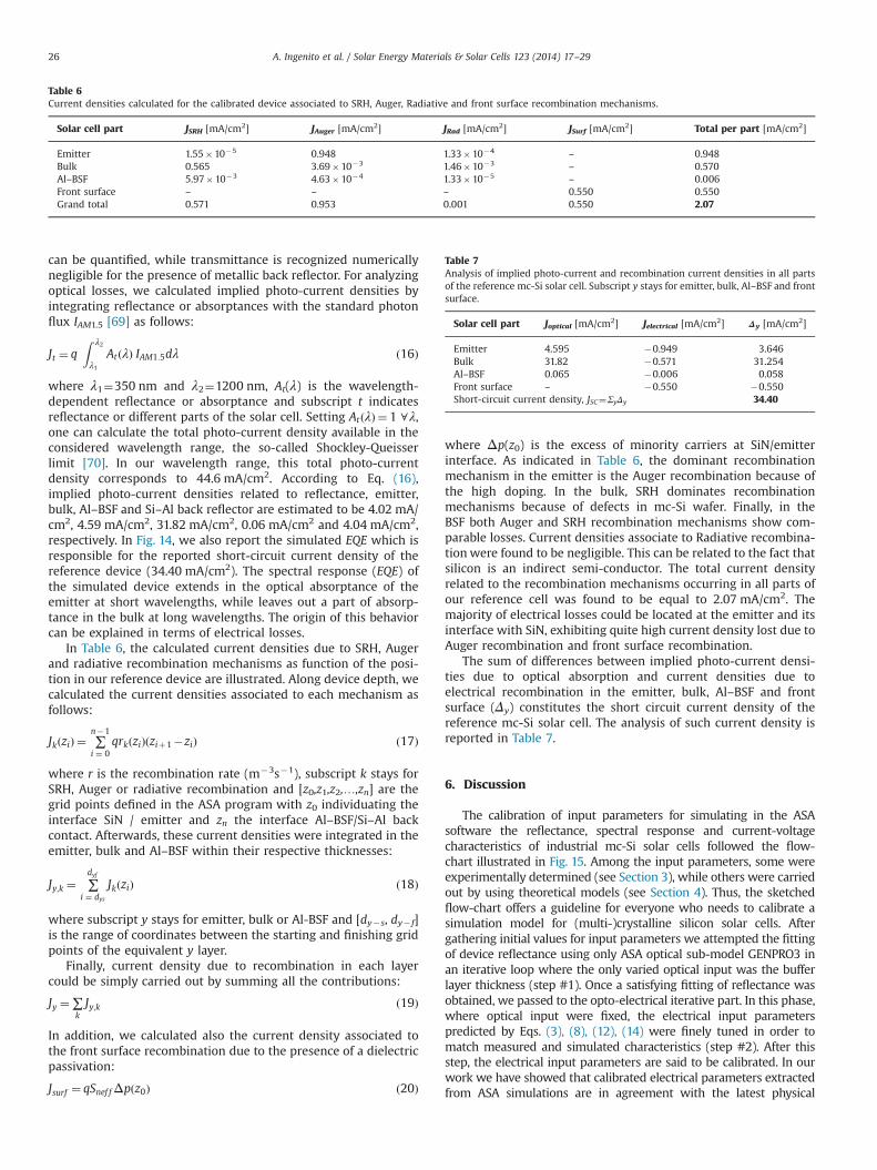
4.3. Opto-electrical modeling of the emitter
Afterwards, we focused on the opto-electrical modeling of theemitter. As depicted in Fig. 1(b), its doping concentration varies overmany orders of magnitude in a narrow region of few hundreds ofnanometers. Such doping profile causes variation in its opticalproperties and recombination mechanisms. From electrical point ofview, as the emitter is heavily doped, the dominant recombinationmechanism is the Auger recombination. In standard illuminationconditions, the excess of carrier concentration in the emitter issmaller than the concentration of donors (ND), which means thatthe device generally operates at low injection conditions. The ASAsoftware calculates the Auger recombination rate as follows [52]:
RAuger ¼ Cnef f n2pþCpef f p
2n ð4Þ
with:
Cnef f ¼ CnND
NDþp
� �þCa
2p
NDþp
� �ð4:aÞ
Cpef f ¼ CpNA
NAþn
� �þCa
2n
NAþn
� �ð4:bÞ
where Cn(p) is the Auger coefficient for electrons (holes) at lowinjection levels, Ca is the ambipolar Auger coefficient at high injectionlevels, n(p) is the thickness dependent concentration of majority(minority) carriers in the emitter (see Fig. 2(a)) and NA is theconcentration of acceptors. Our inputs were the so-called effectiveAuger coefficients Cneff and Cpeff indicated in Eqs. (4.a) and (4.b). Themost quoted values for Auger coefficients are those determined byDziewior and Schmid (Cn¼2.8�10�31 cm6/s and Cp¼0.99�10�31 cm6/s), while the implied ambipolar Auger coefficient can beexpressed as the sum of Cn and Cp (Ca¼3.79�10�31 cm6/s) [53]. Thethickness-dependent carrier lifetime in Auger-dominated emitter isautomatically calculated in ASA as follows [52]:
τemitter ¼1
Cnef f N2D
ð5Þ
Both high doping concentration and low injection condition makethe second factor on the right side of Eq. (4) negligible. DespiteEq. (4) physically describes the Auger recombination, Eqs. (4.a) and(4.b) that model the effective Auger coefficients tend to under-estimate the Auger recombination rate as they do not include theCoulomb enhancement effects at high and low injection levels [54].
The most comprehensive determination of Auger coefficientsfor low injection levels and low doping concentration was pro-posed by Altermatt et al. [55]. They performed an empiricalparameterization of Auger coefficients by multiplying the Dziewiorand Schmid Auger coefficients with the enhancement factors (geeh,gehh) [54,55]. According to this modified model, the Auger recom-bination rate is calculated by replacing Cneff and Cpeff in Eq. (4) withgeehCn and gehhCp, respectively. However, at intermediate dopingconcentration (1�1017 cm�3oNdopo5�1018 cm�3), also thismodified model tends to underestimate the Auger recombinationrate. A more general parameterization of Auger recombination ratefor a wide range of dopant concentration and injection levels wasproposed by Kerr and Cuevas [52]. However, this model does notinclude Coulomb enhancement effects. The model by Richter et al.[56] adds to the model of Kerr & Cuevas [52] the enhancementfactors (geeh, gehh) as introduced by Altermatt. According to Richtermodel, the Auger recombination rate can be written as:
RAuger ¼ np½Cnðn0Þn0þCpðp0Þp0þCaðΔnÞ� ð6Þ
With:
Cnðn0Þ ¼ 2:5� 10�31geehðn0Þ ð6aÞ
Cpðp0Þ ¼ 8:5� 10�32ghheðp0Þ ð6bÞ
CaðΔnÞ ¼ 3� 10�29Δn�0:92 ð6cÞ
where n0 is n in condition of low injection (Δn⪡n0), p0¼ni2/n0, ni is
the intrinsic carrier concentration in silicon and geeh and gehh arethose defined in Altermatt model [54,55]. To strictly implementRichter model in a computer software, one should describe theemitter with many layers, each characterized by (i) thickness equalto the measurement step in the SIMS profile and (ii) dopingconcentration at that specific depth.
Since the emitter is in condition of low injection, the third termon the right side of Eq. (6) is negligible and the values of Augerrecombination in Eq. (6) tend to those of Eq. (4). This means thatusing certain Cn and Cp in the approach implemented in ASA, onecan eventually calculate accurate RAuger for different doping levelsat low injection. To this aim, we split the emitter in sixteen regionsin order to ensure a physically trustworthy modeling of this layer.These sixteen layers in the ASA program had different opticalproperties, doping concentrations and thicknesses. The measuredcomplex refractive index of heavily doped c-Si was used for thefirst two layers of region A which both had a total thickness of16 nm. For the rest of the layers in region A and for the layers in
Emitter depth [nm]0 40 80 120 160 200 240 280 320
Cn
[cm
6 /s]
1.0e-30
2.0e-30
3.0e-30
4.0e-30
5.0e-30
C (N )C (N )C (N )
A B C D
Fig. 8. Cn Auger coefficient for the simulated doping profile predicted by Richtermodel (blue dash-dotted line), Altermatt model (green dashed line) and extractedwith ASA (red solid line). The averaged relative deviation (in the regions A-D)between the Cn extracted with ASA and the Cn calculated with Richter model for thesimulated doping profile was found to be |1-CnASA/CnRicther(sim)|o7%.
Auge
r rec
ombi
natio
n ra
te [c
m-3
s-1]
1e+21
1e+20
1e+19
1e+18
1e+17
1e+16
1e+17
1e+13
1e+12
1e+15
1e+14
1e+13
Emitter depth [nm]
0 40 40 80 120
160
200
240
280
280
320
A B C D
Fig. 9. Auger recombination rate predicted by Altermatt (green dashed line) andRichter (blue dash-dotted line) models compared with the Auger recombinationrate extracted from ASA simulations (red solid line). Auger recombination calcu-lated with Altermatt model showed slightly larger deviation from Richter and ASAmodels in regions A and D.
A. Ingenito et al. / Solar Energy Materials & Solar Cells 123 (2014) 17–2922

regions B–D we used the refractive index of un-doped c-Si (seeFig. 5). Simulated doping concentration in each layer was linearlyapproximated to the SIMS profile as shown in Fig. 2(a). The set ofCn which gave the best fitting between measured and simulatedexternal parameters (see Section 5) is illustrated in Fig. 8 togetherwith Cn predicted by Ricther and Altermatt model calculated forthe simulated doping profile. The Cn extracted with ASA follow thetrend predicted by Ritcher model, showing the capabilities of ourcomputer model in handling both dopant density and injectionlevels. In addition, in Fig. 9 the Auger recombination rate calcu-lated with Richter and Altermatt models were compared with theone simulated by the ASA software. Although based on differentequations, our Auger recombination rate was found to be in goodagreement with Richter rather than Altermatt model.
Finally, aside Auger recombination mechanism, also radiativerecombination was taken into account. It is calculated in ASA as:
Rradiative ¼ Bðnp�n2i Þ ð7Þ
where B is a constant equal to 4.7�10�15 cm�3 s�1 [57]. Thisrecombination mechanism was set for all electrical active layers ofthe simulated device (emitter, bulk and BSF).
4.4. Opto-electrical modeling of the bulk mc-Si
Passing to the bulk region, which is p-type mc-Si in our study,the model parameter describing the bulk recombination is theeffective minority carrier diffusion length (Lneff). Such parameter isused as input in the ASA software by means of the generalrelationship with the minority carrier lifetime in the bulkτbulk ¼ L2nef f =D, where D is the diffusion constant of the minoritycarriers in bulk. In case of high performance front/back sidepassivated c-Si solar cells, this quantity can be approximated withthe minority carrier diffusion length in the bulk (Lb). However, inindustrial mc-Si solar cells, recombination occurs not only at theback side because of the full-area metal contact (see Section 4.5)but also at the boundaries between crystalline grains [57]. Inactual mc-Si material such grains have different shapes, sizes andrecombination activities. This fact leads to a distribution of thevalue of Lneff which is difficult to determine. Therefore, weassumed that the mc-Si bulk is composed of equal grains withidentical electrical properties leading to a unique value of Lneff.
Bulk diffusion length, recombination at grain boundaries andBack Surface Recombination Velocity (BSRV) play a role in describ-ing recombination mechanisms in the bulk and at the backcontact. The overall recombination mechanism can be modeledin terms of effective minority carrier diffusion length as shown inmore detail in Section 4.5.
In this section we describe two subsequent approaches toextract a physically trustworthy value of Lneff without looking atthe aforementioned dependencies. In the first (optical) approach,Lneff was carried out from measured IQE as follows:
dIQE�1
dα�1Si
�����α� 1si ¼ 0
¼ cos ðθÞLnef f
ð8Þ
where α�1si is the absorption length of silicon and θ is the
refraction angle of light into the silicon which is determined bythe front texture [59]. For this angle, we used previously foundaverage value of 401 (see Section 3). The derivative in Eq. (8) istaken for absorption length much shorter than the bulk thickness,to the limit α�1
si -0. In the second (electrical) approach, Lneff wasextracted by fitting measured and simulated external parametersof the reference solar cell, since both VOC and JSC are function of
Lneff [58]. The open-circuit voltage can be expressed as:
VOC ¼kTqln
JLJ0b� rþ J0e
þ1� �
ð9Þ
where JL is the illuminated current density (approximately equal toJsc) and J0b�r and J0e are the saturation current densities of bulk-rear and emitter, respectively. Quantities in Eq. (9) which dependon Lneff are the bulk saturation current and the illuminated currentdensity. The first quantity can be written as:
J0b� r ¼qDn2
i
Lnef f NAð10Þ
where D is the diffusion constant in bulk silicon and NA is the bulkdoping concentration (see Table 3), while the second quantitydepends on Lneff as follows:
JL ¼ qGðLnef f þLpþWscrÞ ð11Þwhere G is the generation-rate profile, Lp is the effective majoritycarriers diffusion length and Wscr is the sum of the widths of thespace charge regions at nþ/p and p/pþ junctions. In this work, weused at first the optical approach to extract the starting value ofLneff for our ASA simulations; afterwards, tuned value of Lneff wasfound by achieving good fitting between measured and simulatedVOC and JSC. Extracted values of Lneff from optical (Eq. (8)) andelectrical approaches (Eqs. (9) and (11)) were, respectively, 441and 418 μm. In the following, we shall use the refined value fromthe electrical approach.
4.5. Opto-electrical modeling of Al–BSF
A typical process used by industry for Al-BSF formation is thescreen printing technique of aluminum followed by rapid thermalannealing. As illustrated in [44], this process leads to the formationof a pþ-Si/Si–Al eutectic/agglomerated Al back contact. In thissection we shall first present how we optically modeled the backreflectance set by Si–Al eutectic [60] and later how we electricallymodeled the Al–BSF.
The optical characterization of Si–Al eutectic layer is not a trivialtask because of its location at the rear side of the solar cell and itsformation on a textured morphology. To model the back reflectancein absence of optical properties of Si–Al eutectic layer, a commonway is to assign a constant value of rear internal reflectance whileBrendel approach [61] or Phong factor [62] can be used fordescribing the light scattering. In this work, we accurately matchedsimulated and measured total reflectance of our reference cell at
Wavelength [nm]400 500 600 700 800 900 1000 1100 1200
R [-
]
0.0
0.2
0.4
0.6
0.8
1.0
Al (simulated) textured
Si-Al / Al (simulated) textured
Si-Al / Al (measured)Si-Al / Al (simulated) flat
Fig. 10. Measured and simulated total reflectance of the reference mc-Si solar cellmeasured at long wavelengths. Flat (textured) in the legend indicates that front andback side are assumed to be flat (textured).
A. Ingenito et al. / Solar Energy Materials & Solar Cells 123 (2014) 17–29 23

wavelengths longer than 900 nm by employing simultaneouslyoptical properties of flat a Si–Al layer [63] and previously men-tioned scattering properties of our textured wafer (see Section 4).We simulated three back reflectors applied to the same solar cellstructure: two modeling the reference cell (Si–Al/Al) with flatinterfaces and rough interfaces, respectively, and one (Si/Al) withtextured interfaces for reference purposes. For the two texturedcases, scattering properties at front and back sides were taken intoaccount. In Fig. 10, the solution comprising Si–Al resulted in loweredreflectance very close to the measured reflectance of our referencecell. As we shall report in Section 5.2, at long wavelengths the Si–Alalloy exhibits considerable absorptance, that is a lower reflectancewith respect to the one based on pure Al. This result also points outthat the reflectivity of the back contact has to be strongly improvedin order to increase the absorption of light in the absorber layer ofthe reference solar cell.
The purpose of a BSF is to electrically reflect the minoritycarriers back in the bulk and to decrease the effective surfacerecombination at the back contact. The BSF essentially decreasesthe high BSRV associated to the full coverage of Al paste(SAl¼107 cm/s) in a lower BSRV at the interface bulk/pþ (Srear-o1000 cm/s) [64]. Although in the ASA program it is not possibleto set the effective surface recombination velocity directly at theinterface bulk/pþ , it is ultimately possible to model this recombi-nation mechanism by using the minority carrier diffusion length inthe bulk. In fact, the Lneff can be expressed as function of Srear bythe following equation [59]:
Lnef f ¼ LbDþSrear Lb tanhðWb=LbÞD tanhðWb=LbÞþSrear Lb
ð12Þ
where Wb is the wafer thickness. Substituting in Eq. (12) therefined value of Lneff previously found, we calculated a value forSrear of 830 cm/s, which is compatible with values reported inliterature for standard full Al–BSF [64]. This proves that theeffective minority carrier diffusion length can be successfully usedas ASA input parameter describing minority carrier diffusionlength of the bulk layer.
When modeling a heavily Al-doped Si, together with SRH andAuger recombination mechanisms, also lateral doping inhomo-geneities and effect of incomplete ionization need to be taken intoaccount [65]. Following a similar approach to that described inSection 4.3 for modeling the emitter, we divided the Al–BSF in tworegions (Y–Z, see Fig. 2(b)) including a total of 7 layers (seeTable 2). In Fig. 11(a) the Cp Auger coefficients calculated accordingto Richter model and the one used in ASA are reported. Theaveraged relative deviation (in the regions Y–Z) between the Cp
extracted with ASA and those calculated with Richter model forthe simulated Al–BSF doping profile was found to be less than 6%.
Regarding the SRH recombination, for low injection conditions anddeep defects level, the minority carrier lifetime equals the minoritycarrier capture time constant [65]. To calculate the SRH minoritycarrier lifetime with such model, the knowledge of the absolute defectconcentration and capture cross section is required. A similar para-meterization of the minority carrier lifetime but as function of the onlyAl doping profile (NAl�BSF) is given by a model by Altermatt [66,67].According to such model, the minority carrier lifetime (τSRH Altermatt)can be analytically expressed as:
τSRH Altermatt
μs¼ 1
ððNAl�BSF Þ=cm�3Þþ2:8339� 10�24fð13Þ
where f is a dimensionless scaling factor given in literature [68]. TheSRH minority carrier lifetime for p-type doped layer is written in theASA program (τSRH ASA) as:
τSRH ASA ¼ τ0NA
Nonset
� �β
ð14Þ
where NA is the acceptor donor concentration and τ0, β and Nonset areconstant. We matched τSRH Altermatt with τSRH ASA as function of thedoping profile by using the set of values: τ0¼1.18e–6s, β¼�1.5,Nonset¼2.3e17 cm�3 and NA¼NAl�BSF, The relative deviation betweenthese two lifetime values calculated as |1-τSRH ASA/τSRH Altermatt | wasfound to be less than 4%. The effective carrier lifetime in Al-BSF(τAl�BSF) can be expressed as:
1τAl�BSF
¼ 1τSRH
þ 1τAuger
ð15Þ
where both τSRH and τAuger are automatically calculated in the ASAprogram from the equivalent recombination mechanism. The effectivecarrier lifetime τAl�BSF is illustrated Fig. 11(b) as function of theposition in Al–BSF, since the doping concentration is variable (seeFig. 2(b)). As the figure depicts, the dominant mechanism of recombi-nation in the Al–BSF region is SRH rather than Auger recombination.The averaged effective lifetime calculated with Eq. (13) for theintermediate doped region was 370 ns, which is in good agreementwith the value found in literature [65].
5. Results
5.1. Calibration results
By using previously calculated or measured input values, weprove in this section that our calibrated model can be used to
Fig. 11. (a) Cp Auger coefficient predicted by Altermatt (green dash-dotted line) and Richter models (pink dashed line). Auger coefficient extracted from ASA simulations inboth Y and Z regions is in a good agreement with Ritcher model (blue solid line). The relative deviation |1-Cp ASA/Cp.Ricther| was found to be less than 6%. (b) Effective lifetimefrom Eq. (13) (blue solid line) and its Auger (τAuger ASA) and SRH (τSRH ASA) components (orange dashed and red dotted lines, respectively) simulated with ASA program.
A. Ingenito et al. / Solar Energy Materials & Solar Cells 123 (2014) 17–2924

simulate industrial mc-Si solar cell. Measured and simulated IQE, Rand illuminated J–V characteristics of reference mc-Si solar cell arepresented in Fig. 12(a) and (b). In Table 4, measured and simulatedexternal parameters of our reference device are summarized,showing an excellent matching.
In addition, we also modeled the dark J–V characteristic of ourreference cell. In Fig. 13, measured and simulated dark currentdensities as function of the voltage are illustrated. Using the basicone-diode model, we found a good matching between simulated andmeasured dark current density only in the voltage range where theseries resistance (Rs) and the shunt resistance (Rsh) are dominant (lightyellow and light purple areas in Fig. 13, respectively). Passing to thetwo-diodes model, which takes into account both leakage currentsand recombination mechanisms [43], we could (i) match measuredand simulated dark J–V curves over the entire voltage range, (ii) extractvalues of current densities J01 and J02 comparable with measured ones,and (iii) find the respective ideality factors η1 and η2 (light blue and
light green areas in Fig. 13, respectively). In Table 5, an overview ofmeasured and simulated electrical parameters related to dark J–Vcharacteristic is reported. Notice that the extracted values of Rs and Rshwere independent from the model used.
5.2. Analysis of the optical and electrical losses of the calibratedmc-Si solar cell
Understanding and quantifying the electrical and optical lossesis crucial for designing new solutions aimed to enhance solar cell0sperformance. In this respect, physically trustworthy opto-electricalsimulations are instrumental for obtaining insights in loss pro-cesses, since measured properties of a solar cell often do not giveclear indications where optical and electrical losses occur in thedevice and of which type.
Fig. 14 illustrates the conservation of energy, intended as sumof reflectance, optical absorptances in all parts of the solar cell andtransmittance. In this type of plot, both optical and electrical losses
IQE
and
R [-
]
0.0
0.2
0.4
0.6
0.8
1.0
MeasuredSimulated
IQE
R
400 500 600 700 800 900 1000 1100 1200 0.0 0.1 0.2 0.3 0.4 0.5 0.6
Cur
rent
den
sity
[mA/
cm2 ]
0
10
20
30
40
MeasuredSimulated
Wavelenth [nm] Voltage [V]
Fig. 12. Measured and simulated (a) IQE and total reflectance (R) and (b) illuminated J–V characteristic of the mc-Si reference solar cell.
Table 4Measured and simulated external parameters of the calibrated mc-Si solar cell.
Measured Simulated
VOC (V) 0.617 0.613JSC (mA/cm2) 34.71 34.40FF (–) 0.773 0.775η (%) 16.55 16.35
Voltage [V]
0.1 0.2 0.3 0.4 0.5 0.6
Dar
k cu
rren
t den
sity
[mA
/cm
2 ]
0.0001
0.001
0.01
0.1
1
10
100
MeasuredSimulated (1-diode model) Simulated (2-diodes model)
Rsh RsJ01 ,η1 J02,η2
Fig. 13. Measured and simulated dark J–V characteristic of the mc-Si reference solarcell. For the regions in light yellow and purple Rs and Rsh are dominant. For the regionsin light blue and green J1 and J2 are dominant. (For interpretation of the references tocolor in this figure legend, the reader is referred to the web version of this article.)
Table 5Measured and simulated external parameters of the calibrated mc-Si solar cell andextracted values from the equivalent circuit.
Rs (Ω) Rsh (Ω) J01(mA/cm2)
J02(mA/cm2)
η1 (–) η2 (–)
Measured 3.84�10�3 60 1.10�10�9 6.4�10�6 – –
Simulated 1 diode 4.13�10�3 115.7 3.8�10�6 – 1.08 –
Simulated 2 diode 4.13�10�3 115.7 2.1�10�9 3.5�10�6 1.01 1.6
Wavelength [nm]400 500 600 700 800 900 1000 1100 1200
R, A
bsor
ptan
ce, L
osse
s [-]
0.0
0.2
0.4
0.6
0.8
1.0
R (4.02 mA/cm )Emitter (4.59 mA/cm )Al-BSF (0.06 mA/cm )Si-Al (4.04 mA/cm )Bulk (31.82 mA/cm )Simulated EQE (34.40 mA/cm )
Fig. 14. Total reflectance and absorptance in all layers of our reference cell togetherwith simulated EQE. Values of implied photo-current density are also reported.
A. Ingenito et al. / Solar Energy Materials & Solar Cells 123 (2014) 17–29 25
can be quantified, while transmittance is recognized numericallynegligible for the presence of metallic back reflector. For analyzingoptical losses, we calculated implied photo-current densities byintegrating reflectance or absorptances with the standard photonflux IAM1.5 [69] as follows:
Jt ¼ qZ λ2
λ1AtðλÞ IAM1:5dλ ð16Þ
where λ1¼350 nm and λ2¼1200 nm, At(λ) is the wavelength-dependent reflectance or absorptance and subscript t indicatesreflectance or different parts of the solar cell. Setting AtðλÞ ¼ 1 8λ,one can calculate the total photo-current density available in theconsidered wavelength range, the so-called Shockley-Queisserlimit [70]. In our wavelength range, this total photo-currentdensity corresponds to 44.6 mA/cm2. According to Eq. (16),implied photo-current densities related to reflectance, emitter,bulk, Al–BSF and Si–Al back reflector are estimated to be 4.02 mA/cm2, 4.59 mA/cm2, 31.82 mA/cm2, 0.06 mA/cm2 and 4.04 mA/cm2,respectively. In Fig. 14, we also report the simulated EQE which isresponsible for the reported short-circuit current density of thereference device (34.40 mA/cm2). The spectral response (EQE) ofthe simulated device extends in the optical absorptance of theemitter at short wavelengths, while leaves out a part of absorp-tance in the bulk at long wavelengths. The origin of this behaviorcan be explained in terms of electrical losses.
In Table 6, the calculated current densities due to SRH, Augerand radiative recombination mechanisms as function of the posi-tion in our reference device are illustrated. Along device depth, wecalculated the current densities associated to each mechanism asfollows:
JkðziÞ ¼ ∑n�1
i ¼ 0qrkðziÞðziþ1�ziÞ ð17Þ
where r is the recombination rate (m�3s�1), subscript k stays forSRH, Auger or radiative recombination and [z0,z1,z2,…,zn] are thegrid points defined in the ASA program with z0 individuating theinterface SiN / emitter and zn the interface Al–BSF/Si–Al backcontact. Afterwards, these current densities were integrated in theemitter, bulk and Al–BSF within their respective thicknesses:
Jy;k ¼ ∑dyf
i ¼ dys
JkðziÞ ð18Þ
where subscript y stays for emitter, bulk or Al-BSF and [dy�s, dy� f]is the range of coordinates between the starting and finishing gridpoints of the equivalent y layer.
Finally, current density due to recombination in each layercould be simply carried out by summing all the contributions:
Jy ¼∑kJy;k ð19Þ
In addition, we calculated also the current density associated tothe front surface recombination due to the presence of a dielectricpassivation:
Jsurf ¼ qSnef fΔpðz0Þ ð20Þ
where Δp(z0) is the excess of minority carriers at SiN/emitterinterface. As indicated in Table 6, the dominant recombinationmechanism in the emitter is the Auger recombination because ofthe high doping. In the bulk, SRH dominates recombinationmechanisms because of defects in mc-Si wafer. Finally, in theBSF both Auger and SRH recombination mechanisms show com-parable losses. Current densities associate to Radiative recombina-tion were found to be negligible. This can be related to the fact thatsilicon is an indirect semi-conductor. The total current densityrelated to the recombination mechanisms occurring in all parts ofour reference cell was found to be equal to 2.07 mA/cm2. Themajority of electrical losses could be located at the emitter and itsinterface with SiN, exhibiting quite high current density lost due toAuger recombination and front surface recombination.
The sum of differences between implied photo-current densi-ties due to optical absorption and current densities due toelectrical recombination in the emitter, bulk, Al–BSF and frontsurface (Δy) constitutes the short circuit current density of thereference mc-Si solar cell. The analysis of such current density isreported in Table 7.
6. Discussion
The calibration of input parameters for simulating in the ASAsoftware the reflectance, spectral response and current-voltagecharacteristics of industrial mc-Si solar cells followed the flow-chart illustrated in Fig. 15. Among the input parameters, some wereexperimentally determined (see Section 3), while others were carriedout by using theoretical models (see Section 4). Thus, the sketchedflow-chart offers a guideline for everyone who needs to calibrate asimulation model for (multi-)crystalline silicon solar cells. Aftergathering initial values for input parameters we attempted the fittingof device reflectance using only ASA optical sub-model GENPRO3 inan iterative loop where the only varied optical input was the bufferlayer thickness (step #1). Once a satisfying fitting of reflectance wasobtained, we passed to the opto-electrical iterative part. In this phase,where optical input were fixed, the electrical input parameterspredicted by Eqs. (3), (8), (12), (14) were finely tuned in order tomatch measured and simulated characteristics (step #2). After thisstep, the electrical input parameters are said to be calibrated. In ourwork we have showed that calibrated electrical parameters extractedfrom ASA simulations are in agreement with the latest physical
Table 6Current densities calculated for the calibrated device associated to SRH, Auger, Radiative and front surface recombination mechanisms.
Solar cell part JSRH [mA/cm2] JAuger [mA/cm2] JRad [mA/cm2] JSurf [mA/cm2] Total per part [mA/cm2]
Emitter 1.55�10�5 0.948 1.33�10�4 – 0.948Bulk 0.565 3.69�10�3 1.46�10�3 – 0.570Al–BSF 5.97�10�3 4.63�10�4 1.33�10�5 – 0.006Front surface – – – 0.550 0.550Grand total 0.571 0.953 0.001 0.550 2.07
Table 7Analysis of implied photo-current and recombination current densities in all partsof the reference mc-Si solar cell. Subscript y stays for emitter, bulk, Al–BSF and frontsurface.
Solar cell part Joptical [mA/cm2] Jelectrical [mA/cm2] Δy [mA/cm2]
Emitter 4.595 �0.949 3.646Bulk 31.82 �0.571 31.254Al–BSF 0.065 �0.006 0.058Front surface – �0.550 �0.550Short-circuit current density, JSC¼ΣyΔy 34.40
A. Ingenito et al. / Solar Energy Materials & Solar Cells 123 (2014) 17–2926
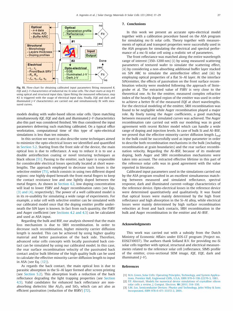
models dealing with wafer-based silicon solar cells. Upon matchingsimultaneously IQE, EQE and dark and illuminated J–V characteristicsalso this part was considered finished. We thus considered the inputparameters delivering such matching calibrated. On a typical officeworkstation, computational time of this type of opto-electricalsimulations is less than ten minutes.
In this section we want to also describe some techniques aimedto minimize the opto-electrical losses we identified and quantifiedin Section 5.2. Starting from the front side of the device, the mainoptical loss is due to reflectance. A way to reduce it is to use adouble antireflection coating or novel texturing techniques asblack silicon [51]. Passing to the emitter, such layer is responsiblefor considerable electrical losses spectrally located at short wave-lengths. The approach employed to decrease such losses is theselective emitter [71], which consists in using two different dopedregions: one highly doped beneath the front metal fingers to keepthe contact resistance low and one lightly doped between themetal fingers. As shown in Section 4.2, low doping concentrationwill lead to lower FSRV and Auger recombination rates (see Eqs.(3) and (4), respectively). The power of a well calibrated model isin its re-usability for simulating a wide range of experiments. Forexample, a solar cell with selective emitter can be simulated withour calibrated model once that the doping emitter profile under-neath the SiN layer is known. In fact from such quantity, the FSRVand Auger coefficient (see Sections 4.2 and 4.3) can be calculatedand used as ASA input.
Regarding the bulk and BSF, our analysis showed that the mainloss mechanism is due to SRH recombination. In order todecrease such recombination, higher minority carrier diffusionlength is needed. This can be achieved by using higher qualitymaterial and better passivation of the back side. Therefore,advanced solar cells concepts with locally passivated back con-tact can be simulated by using our calibrated model. In this case,the rear surface recombination velocity of the passivated backcontact and/or bulk lifetime of the high quality bulk can be usedto calculate the effective minority carrier diffusion length to inputin ASA (see Eq. (12)).
As regards the back contact, the main optical loss is due toparasitic absorption in the Si–Al layer formed after screen printing(see Section 5.2). This absorption leads a reduction of the backreflectance degrading the light trapping properties (see Section4.5). Valid candidates for enhanced back reflectance are non-absorbing dielectric like Al3O2 and SiO2 which can act also asefficient passivation (reduction of the BSRV) [72].
7. Conclusions
In this work we present an accurate opto-electrical modeltogether with a calibration procedure based on the ASA programfor simulating mc-Si solar cells. Theory together with measure-ments of optical and transport properties were successfully used inthe ASA program for simulating the electrical and spectral perfor-mance of a mc-Si solar cell using a realistic set of parameters.
The front reflectance was matched along the entire wavelengthrange of interest (350–1200 nm) (i) by using measured scatteringparameters of textured wafer to simulate the scattering effect,(ii) by considering a non-absorbing additional buffer layer stackedon SiN ARC to simulate the antireflective effect and (iii) byemploying optical properties of a flat Si–Al layer. At the interfaceSiN/emitter, the effects of passivation on the front surface recom-bination velocity were modeled following the approach of Stein-grube et al. The extracted value of FSRV is very close to thetheoretical one. As for the emitter, measured complex refractiveindex of the heavily doped region of the emitter was used in orderto achieve a better fit of the measured EQE at short wavelengths.For the electrical modeling of the emitter, SRH recombination wasfound to be negligible while Auger recombination played a majorrole. By finely tuning the Auger coefficients, a good matchingbetween measured and simulated curves was achieved. The Augerrecombination rate carried out with our modeling was in goodagreement with recent Richter model which can handle a widerange of doping and injection levels. In case of bulk Si and Al–BSF,we proved that the effective minority carrier diffusion length Lneffin the bulk could be successfully used as input parameter in orderto describe both recombination mechanisms in the bulk (includingrecombination at grain boundaries) and the rear surface recombi-nation velocity. Regarding the Al–BSF, because of its moderatedoping, both Auger and SRH recombination mechanisms weretaken into account. The extracted effective lifetime in this part ofthe reference solar cells was in good agreement with the valuereported in literature.
Calibrated input parameters used in the simulations carried outby the ASA program resulted in an excellent simultaneous match-ing between measured and simulated reflectance, spectralresponse, dark and illuminated current–voltage characteristics ofthe reference device. Opto-electrical losses in the reference devicewere determined quantitatively and qualitatively. It was foundthat optical losses were mainly determined by the high frontreflectance and high absorption in the Si–Al alloy, while electricallosses were mainly determined by high surface recombinationvelocities at front and back contacts, SRH recombination in thebulk and Auger recombination in the emitter and Al–BSF.
Acknowledgments
This work was carried out with a subsidy from the DutchMinistry of Economic Affairs under EOS-LT program (Project no.EOSLT10037). The authors thank Solland B.V. for providing mc-Sisolar cells together with optical, structural and electrical measure-ments related to the reference solar cell (reflectance, SIMS profileof the emitter, cross-sectional SEM image, IQE, EQE, dark andilluminated J–V).
References
[1] M.A. Green, Solar Cells: Operating Principles, Technology, and System Applica-tions, Prentice Hall, Englewood Cliffs, U.S.A, ISBN 978-0-138-22270-3, 1981.
[2] P.P. Altermatt, Models for numerical device simulations of crystalline siliconsolar cells a review, J. Comput. Electron. 10 (2011) 314–330.
[3] S.M. Sze, Semiconductor Devices: Physics and Technology, John Wiley & SonsIncorporated, ISBN 978-0-471-33372-2, 2001.
Fig. 15. Flow-chart for obtaining calibrated input parameters fitting measured R,EQE and J–V characteristics of industrial mc-Si solar cells. The chart starts at step #1using optical and structural input data. Upon fitting the measured reflectance, step#2 is triggered with the usage of electrical input data. Finally, EQE and dark andilluminated J–V characteristics are carried out and simultaneously fit with mea-sured curves.
A. Ingenito et al. / Solar Energy Materials & Solar Cells 123 (2014) 17–29 27
[4] B.E. Pieters, H. Stiebig, M. Zeman, R.A.C.M.M. van Swaaij, Determination of themobility gap of intrinsic mc-Si:H in p–i–n solar cells, J. Appl. Phys. 105 (2009)044502, http://dx.doi.org/10.1063/1.3078044.
[5] M. Zeman, R. Van Swaaij, E. Schroten, L.L.A. Vosteen, J.W. Metselaar, Devicemodeling of a-Si:H alloy solar cells: calibration procedure for determination ofmodel input parameters, in: Materials Research Society Symposium Proceed-ings, vol. 507 1998, pp. 409–414, http://dx.doi.org/10.1557/PROC-507-409.
[6] M. Zeman, J. Krč, Optical and electrical modeling of thin-film silicon solar cells,J. Mater. Res. 23 (2008) 889–898, http://dx.doi.org/10.1557/jmr.2008.0125.
[7] O. Isabella, H. Sai, M. Kondo, M. Zeman, Full-wave optoelectrical modeling ofoptimized flattened light-scattering substrate for high efficiency thin-filmsilicon solar cells, Prog. Photovolt. Res. Appl. (2013), http://dx.doi.org/10.1002/pip.2314.
[8] Atlas Silvaco, ⟨http://www.silvaco.com/products/device_simulation/atlas.html⟩.[9] Sentaurus Synopsys, ⟨http://www.synopsys.com/tools/tcad/Pages/default.aspx⟩.[10] M. Peters, M. Rüdiger, H. Hauser, M. Hermle, B. Bläsi, Diffractive gratings for
crystalline silicon solar cells—optimum parameters and loss mechanisms,Prog. Photovolt. Res. Appl. 20 (7) (2012) 862–873, http://dx.doi.org/10.1002/pip.1151.
[11] MicroTec Siborg Systems Inc, ⟨http://www.siborg.com/⟩.[12] H.K. Gummel, A self-consistent iterative scheme for one-dimensional steady
state transistor calculations. Electron devices, IEEE Trans. 11 (10) (1964)455–465, http://dx.doi.org/10.1109/T-ED.1964.15364.
[13] J.G. Fossum, Computer-aided numerical analysis of silicon solar cells, SolidState Electron. 19 (1976) 269–277.
[14] J.G. Fossum, Physical operation of back-surface-field silicon solar cells, ElectronDevices, IEEE Trans. 24 (1977) 322–325.
[15] M.S. Lundstrom, Numerical analysis of silicon solar cells, School of ElectricalEngineering, , 1980. (Ph.D. thesis).
[16] K. Girardini, S. Jacobsen, Tech. Rep. N87-22301, NASA, Scientific and TechnicalInformation (STI), 1986.
[17] PC-1D, ⟨http://www.pv.unsw.edu.au/info-about/our-school/products-services/pc1d⟩.
[18] P.A. Basore, D.T. Rover, A.W. Smith, PC-1D: Enhanced numerical solar cellmodelling, in Proceddings of the Photovoltaic Specialists Conference, Con-ference Record of the Twentieth IEEE 1, 1988, pp. 389–396, DOI: 10.1109/PVSC.1988.105730.
[19] P.A. Basore, Numerical modeling of textured silicon solar cells using PC-1D.Electron Devices, IEEE Trans. 37 (2) (1990) 337–343, http://dx.doi.org/10.1109/16.46362.
[20] C.S. Baker-Finch, K.R. McIntosh, M.L. Terry, Isotextured silicon solar cellanalysis and modeling 1: optics, IEEE J. Photovolt. 2 (2012) 457–464, http://dx.doi.org/10.1109/JPHOTOV.2012.2206569.
[21] C.S. Baker-Finch, K.R. McIntosh, M.L. Terry, Y. Wan, Isotextured siliconsolar cell analysis and modeling 2: recombination and device modeling,IEEE J. Photovolt. 2 (2012) 465–472, http://dx.doi.org/10.1109/JPHOTOV.2012.2204390.
[22] A. Froitzheim, R. Stangl, M. Kriegel, L. Elstner, W. Fuhs, AFORS-HET: acomputer-program for the simulation of heterojunction solar cells to bedistributed for public use, in: Photovoltaic Energy Conversion, Proceedingsof 3rd World Conference on 1 2003, pp. 279–282.
[23] A.G. Aberle, G. Heiser, M.A. Green, Two‐dimensional numerical optimizationstudy of the rear contact geometry of high‐efficiency silicon solar cells, J. Appl.Phys. 75 (1994) 5391, http://dx.doi.org/10.1063/1.355694.
[24] G. Heiser, A.G. Aberle, S.R. Wenham, M.A. Green, Two-dimensional numericalsimulations of high-efficiency silicon solar cells, Microelectron. J. 26 (1995)273–286.
[25] J. Zhao, A. Wang, P. Altermatt, M.A. Green, 24% efficient silicon solar cells withdouble layer antireflection coatings and reduced resistance loss, Appl. Phys.Lett. 66 (26) (1995) 3636–3638, http://dx.doi.org/10.1063/1.103610.
[26] A.G. Aberle, P. Altermatt, G. Heiser, S. Robinson, A. Wang, J. Zhao, U. Krumbein,M.A. Green, Limiting loss mechanisms in 23% efficient silicon solar cells,J. Appl. Phys. 77 (7) (1995) 3491–3504, http://dx.doi.org/10.1063/1.358643.
[27] PV Lighthouse portal, ⟨http://www.pvlighthouse.com.au/⟩.[28] J.O. Schumacher, S. Sterk, B. Wagner, W. Warta, Quantum efficiency analysis of
high efficiency solar cells with textured surfaces, in: Proceedings of the 13thEuropean Photovoltaic Solar Energy Conference, 1 1995, pp. 96–99, ISBN:0-9521452-7-8.
[29] A.W. Smith, A. Rohatgi, S.C. Neel, Texture: a ray traacing program for thephotovoltaic community, Photovoltaic Specialists Conference, in: ConferenceRecord of the Twenty First IEEE 1 (1990), 426–431, http://dx.doi.org/10.1109/PVSC.1990.111660.
[30] R. Brendel, Sunrays: a versatile tray tracing program for the photovoltaiccommunity, in: Proceedings of the 12th European Photovoltaic Solar EnergyConference, 1994, pp. 1339–1342.
[31] J.E. Cotter, Raysim 6.0—a free geometrical ray tracing program for silicon solarcells, Photovoltaic Specialists Conference, in: Conference Record of the ThirtyFirst IEEE, 2005, pp. 1165–1168, http://dx.doi.org/10.1109/PVSC.2005.1488345.
[32] C. Zechner, P. Fath, G. Willeke, E. Bucher, Two- and three-dimensional opticalcarrier generation determination in crystalline silicon solar cells, Sol. Energy Mater.Sol. Cells 51 (1998) 255–267, http://dx.doi.org/10.1016/S0927-0248(97)00226-2.
[33] H. Holst, P.P. Altermatt, R. Brendel, Daidalos—a plugin based framework forextendable ray tracing, in: Proceedings of the 25th European PhotovoltaicSolar Energy Conference, 2010, pp. 2150–2153, http://dx.doi.org/10.4229/25thEUPVSEC2010-2CV.3.24.
[34] B. Lipovšek, J. Krč, M. Topič, Design and optimisation of thin-film silicon pvmodules with surface-textured front glass by using a combined geometricoptics/wave optics model, in: Proceedings of the 27th European PhotovoltaicSolar Energy Conference and Exhibition, 2012, 2604–2607, http://dx.doi.org/10.4229/27thEUPVSEC2012-3DV.1.62.
[35] M. Otto, M. Kroll, T. Käsebier, R. Salzer, A. Tünnermann, R.B. Wehrspohn,Extremely low surface recombination velocities in black silicon passivated byatomic layer deposition, Appl. Phys. Lett. 100 (2012) 191603, http://dx.doi.org/10.1063/1.4714546.
[36] J. Krč, M. Zeman, F. Smole, M. Topič, Optical modeling of a-Si:H solar cellsdeposited on textured glass/SnO2 substrates, J. Appl. Phys. 92 (2002) 749, http://dx.doi.org/10.1063/1.1487910.
[37] F. Leblanc, J. Perrin, J. Schmitt, Numerical modeling of the optical properties ofhydrogenated amorphous‐silicon‐based p‐i‐n solar cells deposited on roughtransparent conducting oxide substrates, J. Appl. Phys. 75 (1994) 1074, http://dx.doi.org/10.1063/1.356489.
[38] J. Krč, F. Smole, M. Topič, Potential of light trapping in microcrystalline siliconsolar cells with textured substrates, Prog. Photovolt. Res. Appl. 11 (7) (2003)429–436, http://dx.doi.org/10.1002/pip.506.
[39] ASA simulator, User0s manual v5.3, Delft University of Technology, 2012,⟨http://www.pvmd.org/forum/⟩.
[40] J. Springer, A. Poruba, M. Vanecek, Improved three-dimensional optical modelfor thin-film silicon solar cells, J. Appl. Phys. 96 (2004) 5329, http://dx.doi.org/10.1063/1.1784555.
[41] K. Jager, M. Zeman, A scattering model for surface-textured thin films, Appl.Phys. Lett. 95 (17) (2009), http://dx.doi.org/10.1063/1.3254239.
[42] S. Selberherr, Analysis and Simulation of Semiconductor Devices, Springer-Verlag, https://ftp.rush.edu/users/molebio/Bob_Eisenberg/Selberherr%20Chap-ter.pdf, ISBN 3-211-81800-6, 1984.
[43] K.R. McIntosh, University of New South Wales, 2001. (PhD thesis), http://books.google.nl/books?id=v9A8NQAACAAJ.
[44] B. Sopori, National Renewable Energy Laboratory (U.S.), Studies on backsideAl-contact formation in Si solar cells: fundamental mechanisms, in: MaterialsResearch Society Symposium Proceedings 1123, 2009, pp. 7–11, http://dx.doi.org/10.1557/PROC-1123-1123-P07-11.
[45] F. Huster, G. Schubert, ECV doping profile measurements of aluminum alloyedback surface field, in: Proceedings of the 20th European Photovoltaic SolarEnergy Conference and Exhibition, 2005, 2DV2.48.
[46] K. Jäger, O. Isabella, R.A. C.M. M. van Swaaij, M. Zeman, Angular resolvedscattering measurements of nano-textured substrates in a broad wavelengthrange, Meas. Sci. Technol. 22 (2011) 105601, http://dx.doi.org/10.1088/0957-0233/22/10/105601.
[47] L. Viña, M. Cardona, Effect of heavy doping on the optical properties and theband structure of silicon, Phys. Rev. B 29 (1984) 12, http://dx.doi.org/10.1103/PhysRevB.29.6739.
[48] R. Hezel, K. Jaeger, Low-temperature surface passivation of silicon for solarcells, J. Electrochem. Soc. 136 (1989) 518–523, http://dx.doi.org/10.1149/1.2096673.
[49] S. Steingrube, P.P. Altermatt, D.S. Steingrube, J. Schmidt, R. Brendel, Inter-pretation of recombination at c-Si/SiNx interfaces by surface damage, J. Appl.Phys. 108 (2010) 014506, http://dx.doi.org/10.1063/1.3437643.
[50] M.J. Kerr, A. Cuevas, Recombination at the interface between silicon andstoichiometric plasma silicon nitride, Semicond. Sci. Technol. (2002), http://dx.doi.org/10.1088/0268-1242/17/2/314.
[51] O. Jihun, Y. Hao-Chih, M. Howard, An 18.2%-efficient black-silicon solar cellachieved through control of carrier recombination in nanostructures, Nat.Nanotechnol. 7 (2012) 743–748, http://dx.doi.org/10.1038/nnano.2012.166.
[52] M.J. Kerr, A. Cuevas, General parameterization of Auger recombination incrystalline silicon, J. Appl. Phys. 91 (2002) 2473, http://dx.doi.org/10.1063/1.1432476.
[53] J. Dziewior, W. Schmid, Auger coefficients for highly doped and highly excitedsilicon, Appl. Phys. Lett. 31 (1977) 346, http://dx.doi.org/10.1063/1.89694.
[54] P.P. Altermatt, S. Ronald, A.G. Heiser, Improvements in numerical modeling ofhighly injected crystalline silicon solar cells, Sol. Energy Mater. Sol. Cells 65(2001) 149–255, http://dx.doi.org/10.1016/S0927-0248(00)00089-1.
[55] P.P. Altermatt, J. Schmidt, G. Heiser, A.G. Aberle, Assessment and parameter-ization of Coulomb-enhanced Auger recombination coefficients in lowlyinjected crystalline silicon, J. Appl. Phys. 82 (1997) 4938, http://dx.doi.org/10.1063/1.366360.
[56] A. Richter, S.W. Glunz, F. Werner, J. Schmidt, A. Cuevas, Improved quantitativedescription of Auger recombination in crystalline silicon, Phys. Rev. B 86(2012) 165202, http://dx.doi.org/10.1103/PhysRevB.86.165202.
[57] T. Trupke, M.A. Green, P. Würfel, P.P. Altermatt, A. Wang, J. Zhao, R. Corkish,Temperature dependence of the radiative recombination coefficient of intrin-sic crystalline silicon, J. Appl. Phys. 94 (2003) 4930–4937, http://dx.doi.org/10.1063/1.1610231.
[58] R. Brendel, Thin Film Crystalline Silicon Solar Cell, Wiley-VCH, Weinheim,ISBN 978-3-527-40376-9, 2003.
[59] P.A. Basore, Extended spectral analysis of internal quantum efficiency, in:Photovoltaic Specialists Conference, Conference Record of the Twenty ThirdIEEE, 1993, pp. 147–152, http://dx.doi.org/10.1109/PVSC.1993.347063.
[60] F. Huster, Investigation of the alloying process of screen printed aluminumpastes for the BSF formation on silicon solar cells, in: Proceedings of the 20thEuropean Photovoltaic Solar Energy Conference and Exhibition, 2005,2DV2.49.
A. Ingenito et al. / Solar Energy Materials & Solar Cells 123 (2014) 17–2928

[61] R. Santbergen, Optical Absorption Factor of Solar Cells for PVT Systems, (PhDthesis), Eindhoven University of Technology, 2008, http://alexandria.tue.nl/extra2/200811936.pdf ISBN: 978-90-386-1467-0.
[62] D. Kray, M. Hermle, W. Glunz, Theory and experiments on the back sidereflectance of silicon wafer solar cells, Prog. Photovolt. Res. Appl. 16 (2008)1–15, http://dx.doi.org/10.1002/pip.769.
[63] ⟨http://refractiveindex.info/?group=CRYSTALS&material=AlSi⟩.[64] V. Meemongkolkiata, K. Nakayashikia, D.S. Kima, R. Kopecekb, A. Rohatgi,
Factors limiting the formation of uniform and thick aluminum–back-surfacefield and its potential, J. Electrochem. Soc.153 (2006) 53–58, http://dx.doi.org/10.1149/1.2129106.
[65] M. Rüdiger, M. Rauer, C. Schmiga, M. Hermle, Effect of incomplete ionizationfor the description of highly aluminum-doped silicon, J. Appl. Phys. 110 (2011)024508, http://dx.doi.org/10.1063/1.3603043.
[66] P.P. Altermatt, J.O. Schuhmacher, A. Cuevas, M.J. Kerr, S.W. Glunz, R.R. King,G. Heiser, A. Schenk, Numerical modeling of highly doped Si:P emitters basedon Fermi–Dirac statistics and self-consistent material parameters, J. Appl.Phys. 92 (2002) 3187. (http://dx.doi.org/1063/1.1501743).
[67] P.P. Altermatt, S. Steingrube, Y. Yang, C. Sprodowski, T. Dezhdar, S. Koc, B. Veith,S. Herrman, R. Bock, K. Bothe, J. Schmidt, R. Brendel, Highly predictivemodeling of entire Si solar cells for industrial applications, in: Proceedingsof the 24th European Photovoltaic Solar Energy Conference, 2009, 901–906,http://dx.doi.org/10.4229/24thEUPVSEC2009-2AO.1.1.
[68] R. Bock, P.P. Altermatt, J. Schmidt, R. Brendel, Formation of aluminum–oxygencomplexes in highly aluminum-doped silicon, Semicond. Sci. Technol. 25(2010) 105007, http://dx.doi.org/10.1088/0268-1242/25/10/105007.
[69] Air Mass 1.5 AM1.5G spectra, ⟨http://rredc.nrel.gov/solar/spectra/am1.5/⟩.[70] W. Shockley, H.J. Queisser, Detailed balance limit of efficiency of pn junction
solar cells, J. Appl. Phys. 32 (1961) 510, http://dx.doi.org/10.1063/1.1736034.[71] M.Z. Rahman, Status of selective emitters for p-Type c-Si solar cells, Opt.
Photon. J. 2 (2012) 129–134, http://dx.doi.org/10.4236/opj.2012.22018.[72] T. Dullweber, S. Gatz, H. Hannebauer, T. Falcon, R. Hesse, J. Schmidt, R. Brendel,
19.4% efficient large area rear-passivated screen-printed silicon solar cells, in:Proceedings of the 26th European Photovoltaic Solar Energy Conference andExhibition, 2011, pp. 811–816, http://dx.doi.org/10.4229/26thEUPVSEC2011-2BP.1.4.
A. Ingenito et al. / Solar Energy Materials & Solar Cells 123 (2014) 17–29 29