accelerating the development of transparent graphene...
TRANSCRIPT

SANDIA REPORT SAND2013-7919 Unlimited Release Printed September 2013
Accelerating the Development of Transparent Graphene Electrodes through Basic Science Driven Chemical Functionalization Calvin K. Chan, Thomas E. Beechem, Taisuke Ohta, Michael T. Brumbach, Alexander Veneman, I. Raluca Gearba, David R. Wheeler, and Keith J. Stevenson Prepared by Sandia National Laboratories Albuquerque, New Mexico 87185 and Livermore, California 94550 Sandia National Laboratories is a multi-program laboratory managed and operated by Sandia Corporation, a wholly owned subsidiary of Lockheed Martin Corporation, for the U.S. Department of Energy's National Nuclear Security Administration under contract DE-AC04-94AL85000. Approved for public release; further dissemination unlimited.

2
Issued by Sandia National Laboratories, operated for the United States Department of Energy by Sandia Corporation. NOTICE: This report was prepared as an account of work sponsored by an agency of the United States Government. Neither the United States Government, nor any agency thereof, nor any of their employees, nor any of their contractors, subcontractors, or their employees, make any warranty, express or implied, or assume any legal liability or responsibility for the accuracy, completeness, or usefulness of any information, apparatus, product, or process disclosed, or represent that its use would not infringe privately owned rights. Reference herein to any specific commercial product, process, or service by trade name, trademark, manufacturer, or otherwise, does not necessarily constitute or imply its endorsement, recommendation, or favoring by the United States Government, any agency thereof, or any of their contractors or subcontractors. The views and opinions expressed herein do not necessarily state or reflect those of the United States Government, any agency thereof, or any of their contractors. Printed in the United States of America. This report has been reproduced directly from the best available copy. Available to DOE and DOE contractors from U.S. Department of Energy Office of Scientific and Technical Information P.O. Box 62 Oak Ridge, TN 37831 Telephone: (865) 576-8401 Facsimile: (865) 576-5728 E-Mail: [email protected] Online ordering: http://www.osti.gov/bridge Available to the public from U.S. Department of Commerce National Technical Information Service 5285 Port Royal Rd. Springfield, VA 22161 Telephone: (800) 553-6847 Facsimile: (703) 605-6900 E-Mail: [email protected] Online order: http://www.ntis.gov/help/ordermethods.asp?loc=7-4-0#online

3
SAND2013-7919 Unlimited Release
Printed September 2013
Accelerating the Development of Transparent Graphene Electrodes through Basic Science
Driven Chemical Functionalization
Calvin K. Chan, Thomas E. Beechem, Taisuke Ohta, Michael T. Brumbach, David R. Wheeler Sandia National Laboratories
P.O. Box 5800 Albuquerque, New Mexico 87185-MS1415
Alexander Veneman, I. Raluca Gearba, Keith J. Stevenson
Department of Chemistry and Biochemistry The University of Texas at Austin
Austin, Texas 78712
Abstract
Chemical functionalization is required to adapt graphene’s properties to many applications. However, most covalent functionalization schemes are spontaneous or defect driven and are not suitable for applications requiring directed assembly of molecules on graphene substrates. In this work, we demonstrated electrochemically driven covalent bonding of phenyl iodoniums onto epitaxial graphene. The amount of chemisorption was demonstrated by varying the duration of the electrochemical driving potential. Chemical, electronic, and defect states of phenyl-modified graphene were studied by photoemission spectroscopy, spatially resolved Raman spectroscopy, and water contact angle measurement. Covalent attachment rehybridized some of the delocalized graphene sp2 orbitals to localized sp3 states. Control over the relative spontaneity (reaction rate) of covalent graphene functionalization is an important first step to the practical realization of directed molecular assembly on graphene. More than 10 publications, conference presentations, and program highlights were produced (some invited), and follow-on funding was obtained to continue this work.

4
ACKNOWLEDGMENTS The authors thank Guild Copeland, Anthony McDonald, and Lyle Brunke for experimental assistance. Work at Sandia National Laboratories was funded in part by the Early Career Laboratory Directed Research and Development program, LDRD Project Number 155550, Title “Accelerating the Development of Transparent Graphene Electrodes through Basic Science Driven Chemical Functionalization.” Additional funding was provided by the Energy Frontiers Research Center funded by the U.S. Department of Energy, Office of Science, Office of Basic Energy Sciences on “Understanding Charge Separation and Transfer at Interfaces in Energy Materials” (EFRC:CST, Award Number DE-SC0001091). Sandia National Laboratories is a multiprogram laboratory managed and operated by Sandia Corporation, a wholly owned subsidiary of Lockheed Martin Corporation, for the U.S. Department of Energy’s National Nuclear Security Administration under contract DE-AC04-94AL85000. Work at the University of Texas at Austin was funded by the Energy Frontiers Research Center funded by the U.S. Department of Energy, Office of Science, Office of Basic Energy Sciences on “Understanding Charge Separation and Transfer at Interfaces in Energy Materials” (EFRC:CST, Award Number DE-SC0001091).

5
CONTENTS
1. Introduction ................................................................................................................................ 7 1.1. Experimental Approach .................................................................................................. 7 1.2. Programmatic Relevance ................................................................................................ 8
2. Results ........................................................................................................................................ 8 2.1. Background ..................................................................................................................... 8 2.2. Functionalization from Diazonium Precursors ............................................................... 9 2.3. Functionalization from Nitro Phenyl Iodonium Salts ................................................... 10 2.4. Functionalization from Fluorinated Aryl Iodonium Salts ............................................. 11
2.4.1. Experimental Details ....................................................................................... 11 2.4.2. Experimental Results and Discussion ................................................................ 12
3. Conclusions .............................................................................................................................. 19 4. Impact of Research .................................................................................................................. 19 5. References ................................................................................................................................ 20 Appendix A: List of Publications and Presentations ................................................................... 24 Distribution ................................................................................................................................... 25
FIGURES Figure 1. Electrochemical functionalization of ITO with NO2 from an iodonium precursor (left). The reversible NH2 ⇔ NH-OH reaction allows counting of the functionalization density (right)........................................................................................................................................................ 10 Figure 2. XPS of nitrophenyl functionalized ITO. Full scan on left, N 1s in center, O 1s on right........................................................................................................................................................ 11 Figure 3. Proposed reaction pathway for covalent graphene functionalization from trifluoromethylphenyl iodonium. (1) Electron injection from graphene. (2) Dissociation of (CF3Ph)2I+ into CF3Ph iodide and a CF3Ph radical. (3) Covalent attachment of the radical to graphene. ....................................................................................................................................... 13 Figure 4. Cyclic voltammogram of epitaxial graphene/SiC(0001) in acetonitrile containing 10 mM (CF3Ph)2I+BF4
− and 100 mM TBATFB, at a scan rate of 50 mV·s−1. .................................. 14 Figure 5. XPS spectra of F 1s, C 1s C−F, and C 1s C−C regions for (a) as-prepared graphene, (b) dip-treated graphene, (c) CA-treated graphene, and (d) CV-treated graphene. For clarity, the spectra in the C 1s C−C region were normalized and shifted to match the as-prepared graphene peak. Normalization factors a and the shift amounts b are shown in the legend as (a·A,BE-b). . 14

6
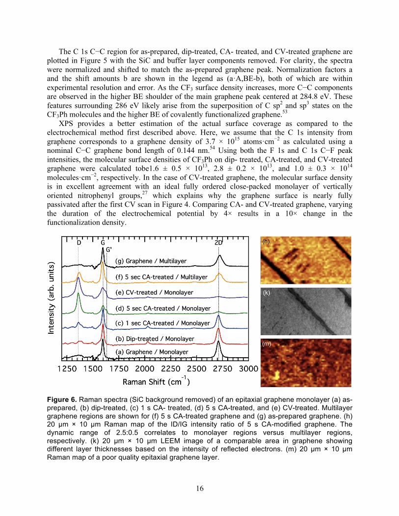
Figure 6. Raman spectra (SiC background removed) of an epitaxial graphene monolayer (a) as-prepared, (b) dip-treated, (c) 1 s CA- treated, (d) 5 s CA-treated, and (e) CV-treated. Multilayer graphene regions are shown for (f) 5 s CA-treated graphene and (g) as-prepared graphene. (h) 20 µm × 10 µm Raman map of the ID/IG intensity ratio of 5 s CA-modified graphene. The dynamic range of 2.5:0.5 correlates to monolayer regions versus multilayer regions, respectively. (k) 20 µm × 10 µm LEEM image of a comparable area in graphene showing different layer thicknesses based on the intensity of reflected electrons. (m) 20 µm × 10 µm Raman map of a poor quality epitaxial graphene layer. ............................................................................................................... 16 Figure 7. UPS spectra of (a) as-prepared graphene, (b) dip-treated graphene, and (c) CV-treated graphene. The vacuum level onset Evac is shown on the left, valence states in the center, and the Fermi level region EF on the right. ............................................................................................... 18
TABLES Table 1. Water contact angles for damaged, untreated, and functionalized epitaxial graphene. . 17

7
1. INTRODUCTION Despite intense research on the fundamental properties of graphene since its isolation in 2004,1 its practical wide-spread application remains elusive. Graphene has been proposed for use as a transparent electrode owing to the material’s high in-plane conductivity, transparency, chemical stability, and elemental abundance. Large interest in this application stems from the desire to replace rare and expensive brittle conducting oxides (e.g., ITO), unstable conducting polymers (e.g., PEDOT:PSS), and fragile optically thin metals as electrical contacts to solar cells, light- emitting diodes, and photodetectors. However, previous efforts in using graphene for electrodes have suffered from poor film quality and uncontrolled interactions between graphene and the contacted materials.2,3 Chemical functionalization is a promising means of modifying and improving graphene’s interaction with other materials, but current functionalization schemes are not well controlled, characterized, or understood.4-7 The practical use of graphene as a transparent electrode material will require controlling the chemical functionalization of graphene interfaces, characterizing the physical properties of the functionalized surfaces, and understanding how modifying graphene’s chemical nature also affects its material and physical properties. This work employs a comprehensive characterization methodology to understand the effects of functionalization chemistry on the material and physical properties of graphene. Of particular interest is how chemical functionalization of graphene affects its electronic band structure and its energy band alignment with other materials. These issues, which are still not well characterized or understood in graphene, greatly affect the material’s conductivity and transparency, as well as charge injection and extraction in devices. We will initially investigate functionalization chemistries intended to modify the work function of graphene and improve its performance as a transparent electrode in optoelectronic devices. Using knowledge generated from fundamental surface science measurements, and correlating functionalization chemistries to material properties, this work will accelerate the systematic development of optimally functionalized graphene films for transparent electrodes and other applications. 1.1. Experimental Approach In an effort to establish a general analytical framework for understanding the relationship between graphene functionalization and its material properties, we will initially study functionalization chemistries relevant for improving the performance of transparent graphene electrodes. Electron withdrawing or electron donating diazonium or iodonium compounds have been selected to increase or decrease graphene’s work function, respectively, so as to improve charge transfer at the contact interface. While diazonium functionalization has been observed on graphene surfaces,4-6 its electrode properties have not been comprehensively characterized, understood, or controlled. Iodonium chemistries have not yet been explored on graphene. In both cases, the attached phenyl rings provide additional sites for further functionalization, such as for surface energy modification. In contrast to other work using poor quality exfoliated or chemical vapor deposited graphene films (ExfG or CVDG) for electrodes,2,3 our approach will functionalize high quality epitaxial graphene (EpiG) grown on silicon-carbide substrates.8 EpiG has significantly lower defect densities than ExfG or CVDG to facilitate the correlation between chemical functionalization and changes in graphene’s intrinsic properties. EpiG is also better suited for transparent electrode applications due to its higher conductivity and transparency.

8
To accelerate the path from discovery to application, our work aims to establish a comprehensive characterization methodology to study the effects of functionalization chemistry on graphene’s electronic and material properties. One of the most important correlations to establish is how chemical functionalization of graphene affects its electronic band structure and its energy band alignment with other materials. Ultraviolet photoemission spectroscopy (UPS) will be developed to investigate the band structure of functionalized graphene films. Chemical characterization of the functionalized films will be needed to correlate how fundamental changes in the chemical bonding environment affect graphene’s band structure and its ensuing physical properties. Using X-ray photoemission spectroscopy (XPS) and Raman spectroscopy, the underlying chemistry behind functionalized graphene films provides the linking step to drive the direction of future efforts to functionalize graphene for specific applications. 1.2. Programmatic Relevance Many technologies driving U.S. innovation, commercial interests, and national security rely heavily on transparent electrodes based on scarce and expensive minerals controlled by foreign entities. Many energy conversion technologies requiring efficient electrical contacts are also needed for a balanced, independent, and sustainable national energy portfolio. Successful leverage of the findings presented in this work to technologically relevant applications will have an immense impact on mitigating our nation’s reliance on foreign resources, and bolster the diversity and sustainability of our own energy resources. This work will also have consequences in wide ranging engineering applications, such as nanoscale processing of graphene for national security applications in nanoelectronics and chemical/biological sensing.
2. RESULTS 2.1. Background Graphene has drawn considerable attention for its unique fundamental properties1 but also for its potential applications in nanoelectronics,2 photonics,3 transparent electrodes,3−8 and sensing.9−12
There is an increasing need to modify graphene’s electronic, chemical, and physical properties to suit specific applications. Chemical functionalization can been exploited to modulate graphene’s bandgap and carrier concentration in transistors; work function and wetting properties for trans- parent electrodes; and chemical sensitivity and specificity for chemical sensors.
Past work on graphene functionalization has fallen into four broad categories: (1) noncovalent functionalization, (2) covalent functionalization of graphene by oxygen to create graphene oxide, (3) the subsequent covalent functionalization of graphene oxide, and (4) direct covalent functionalization. Noncovalent graphene functionalization involves the intercalation or adsorption of charge transfer atoms or molecules. This method is mostly used to modify carrier concentration and work function.13−16 This doping, at least to moderate concentrations, does not appreciably change graphene’s band structure (i.e., open a band gap) or chemical properties. Noncovalent graphene modification has also been explored for improving graphene’s solubility in solution-based processes.17−19
The creation of graphene oxide is a covalent functionalization method often used to improve graphene’s processability. Oxidation of graphene modulates its wettability,20 which facilitates

9
solution-based deposition of thin films.6,21−23 Graphene oxide films can be reduced back to graphene or used as an intermediary for the covalent bonding of molecular compounds through the oxygen sites.24 Despite these benefits, graphene oxidation processes lead to appreciable defects with unpredictable densities, nucleation, aggregation, and chemical structures.25 Even upon reduction back to graphene, the material still contains irreversible damage including point defects and amorphous glassy carbon-like regions. Linking functional groups to graphene via covalent bonds to oxygen is also not always desired.
Direct covalent graphene functionalization by molecular compounds has been more recently explored, usually employing aryl diazonium compounds.26−30 These phenylene-based molecules are desirable for their structural and chemical similarity to graphene and the multitude of phenylene side group attachments. Band gap modification, conductivity enhancements, and processing improvements have been demonstrated using covalent graphene functionalization from aryl diazonium precursors.28,29,31,32 However, diazonium chemistry is readily spontaneous on metal and semiconductor surfaces33 and is fairly spontaneous on graphene.27,34 It is therefore difficult to moderate graphene’s properties simply by modulating the surface functionalization density. Spontaneous diazonium self-assembly is also not well-suited for applications requiring directed assembly of molecules on graphene (e.g., printed graphene circuits, chemical/biological sensor arrays, etc.). As previously shown, control over the relative spontaneity of covalent graphene functionlization, often with orders of magnitude variability in the reaction rate, is desirable for realizing directed molecular assembly on graphene.
Iodonium compounds have higher reduction potentials in comparison to their analogous diazonium salts and have shown nonspontaneous or less spontaneous covalent bonding on Si, Pt, and glassy carbon surfaces.35−38 Here, we demonstrate the electrochemically driven covalent functionalization of graphene from a symmetric aryl iodonium salt. Specifically, epitaxial graphene on SiC(0001) was covalently functionalized with trifluoromethylphenylene (CF3Ph). Unlike the direct covalent graphene functionalization works cited above, most of which employ nitro-terminated molecules, CF3Ph was chosen because its nonreactive, hydrophobic, and electronegative fluorine end groups are technologically important in materials chemistry, surface passivation, and charge transfer applications. Epitaxial graphene was chosen as the substrate to clearly understand the effects of basal plane functionalization on the physicochemical properties of graphene. Shifts in the chemical, electronic, and defect states were observed with photoemission and Raman spectroscopies. An increase in the water contact angle was also observed with increasing functionalization. The changes were consistent with some rehybridization of graphene’s sp2 configuration to covalently bonded sp3 states upon function- alization and the adsorption of fluorine-terminated molecules to the graphene surface. 2.2. Functionalization from Diazonium Precursors As expected, and in agreement with the literature, initial diazonium functionalization experiments showed that the chemistry was too spontaneous for controlling surface coverage on indium tin oxide (ITO) and graphene. As shown by Bekyarova et al,27 the functionalization density could be controlled by submerging the substrates in dilute diazonium solutions over 12-24 hours. We found this to be impractical from a technological standpoint, and immediately shifted the project focus to investigating new iodonium functionalizations of graphene.

10
2.3. Functionalization from Nitro Phenyl Iodonium Salts Preliminary efforts to covalently modify graphene began with the electrochemical grafting of 4-nitrophenyl-iodonium tetrafluoroborate onto indium tin oxide (ITO). As shown in Figure 1, experiments on NO2-functionalized ITO exhibited a well-defined first reduction wave at –900 mV vs. a Ag/Ag+ nonaqueous reference electrode. Subsequent cyclic voltammetric (CV) scans showed attenuation of the reduction peak, but no significant shift in the reduction potential. This suggests stacking of nitrophenyl groups on the ITO surface. The benefit of nitro functional groups is that a reversible electrochemical reaction
NO2 ⇒ NH2
NH2 ⇔ NH-OH
can be used to quantify the surface functionalization density. The molecular density can be estimated from the charge Q passed through the electrochemical cell
Q = nFAΓ/NA
where Q = 5.77 x 10⁻⁵ Coul is determined by the area under the reduction peak after subtraction of a linear background. Additionally, n = 6 for the six-electron NH2 ⇔ NH-OH reaction; A ≈ 0.8 cm2 for the area of the ITO electrode; F is Faraday’s constant; NA is Avogadro’s constant; and Γ is the surface density of electrochemically activated reactants. From this, we determine that the surface coverage was ~ 7.8 × 10¹³ molecules cm-2. This is approximately one order of magnitude less than the close-packed surface coverage expected for nitrophenyl groups.27
Figure 1. Electrochemical functionalization of ITO with NO2 from an iodonium precursor (left). The reversible NH2 ⇔ NH-OH reaction allows counting of the functionalization density (right).

11
Figure 2. XPS of nitrophenyl functionalized ITO. Full scan on left, N 1s in center, O 1s on right.
X-ray photoemission spectroscopy (XPS) on NO2-phenylene functionalized ITO showed significant charging of the film (Figure 2, left), suggesting the deposition of a thick NO2 film on the ITO. Quantitative analysis of the N 1s (Figure 2, center) and O 1s (Figure 2, right) spectra show a N:O ratio of 2.7, which is unexpectedly high compared the 0.5 N:O ratio for NO2. Since NO2 is an electrochemically active species, we suspect that polymerization of NO2-phenylenes is occurring as depicted in the inset of the full scan in Figure 2. This would lead to the lower molecular surface density calculated using the electrochemical method described above, since more of the NO2 sites are tied up in self-linking to other nitrophenyl groups. Due to the self-functionalization of nitrophenyl groups, we found this approach not suitable for well-controlled functionalization of graphene. 2.4. Functionalization from Fluorinated Aryl Iodonium Salts In an attempt to control the functionalization density of graphene, we developed a method to synthesize and electrochemically activate CF3Ph-iodonium precursors on graphene. 2.4.1. Experimental Details Graphene was epitaxially grown on 6H-SiC(0001) by the sublimation of Si in an Ar environment.39 N-type SiC(0001) with a nominal sheet resistance of 0.1 Ω cm (Cree, Inc.) was first annealed in 1 atm of 45% H2:Ar at 1450 °C to remove polishing-induced surface damage. Graphitization was then achieved by heating to 1550 °C in the presence of ultrahigh purity Ar at atmospheric pressure. Graphene films were examined using low-energy electron microscopy (LEEM) and atomic force microscopy (AFM) to verify film thickness and quality. All samples used in this study exhibited single monolayer (ML) graphene on approximately 80% of the sample surface area and multilayer graphene (2−3 ML) primarily at SiC step edges. The graphene monolayer is a single continuous sheet that conforms to the underlying terrace structure of SiC.40

12
Electrochemical covalent functionalization of graphene was achieved by electrochemical reduction of bis(4-trifluoromethyl- phenyl) iodonium tetrafluoroborate [(CF3Ph)2I+BF4
−] dis- solved in solution. The iodonium salt precursor was synthesized using a one-pot synthesis method described by Bielawski et al.41 The electrochemical solution contained 10 mM (CF3Ph)2I+BF4
− in anhydrous acetonitrile (ACN), with 100 mM tetrabutylammonium tetrafluoroborate (TBATFB) as a supporting electrolyte. Epitaxial graphene/SiC(0001) was the working electrode, while electrochemical potentials and currents were measured with a Ag/Ag+ reference electrode and a Pt counter electrode, respectively (Bioanalytical Systems, Inc.). The cell solution was purged with Ar for at least 15 min before inserting the substrate, and the electrochemical reaction was conducted in a nominal Ar environment to prevent incidental oxidation of graphene and the functional molecules. The electrochemical cell was emptied and refilled with fresh CF3PhI+BF4
− ACN solution after the treatment of one to two samples. Cyclic voltammetric (CV) and chronoamperometric (CA) methods were used to initiate the electrochemical reaction.
X-ray photoemission spectroscopy (XPS) was performed in a Kratos Axis Ultra DLD system using monochromated Al Kα irradiation (hν = 1486.6 eV) and a hemispherical electron energy analyzer. Spectral intensities were normalized by each core level’s respective photoionization atomic sensitivity factors, i.e., σF1s = 1.000 and σC1s = 0.296. Qualitative and quantitative chemical analysis of the C 1s spectra was aided by background and spectral subtraction to isolate features associated with functionalized graphene from the SiC, the buffer layer, and surface-adsorbed hydrocarbon components.42−47 First, Shirley backgrounds were computed and subtracted from each C 1s spectra. Then, the underlying SiC, buffer layer, and surface adsorbed hydrocarbon components were identified by sub- tracting the graphene carbon peak as referenced to a C 1s spectrum of chemical vapor deposited graphene on Ni. This composite SiC, buffer layer, and hydrocarbon background were then subtracted from the functionalized epitaxial graphene spectra.
Ultraviolet photoemission spectroscopy (UPS) was performed in the XPS system using an Omicron GmbH differentially pumped He plasma discharge lamp. Electron kinetic energies collected by the analyzer were converted to binding energies by referencing to the system’s Fermi level (EF) as measured on clean metal substrates (Au, Ag, Cu). Work functions were calculated by subtracting the vacuum level onset (Evac) observed at high binding energy from the HeI photon energy (hν = 21.22 eV).
Spatially resolved Raman spectroscopy was carried out using a WiTec GmbH alpha300R confocal Raman system having a spectral resolution of ≈3 cm−1 using 532 nm irradiation focused to a ≈ 700 nm diameter spot. Laser powers were optimized to prevent sample damage. Scans were conducted every 333 nm across 15 µm × 15 µm regions. Water contact angle measurements were conducted using a Rame-Hart goniometer. Ultrahigh purity water with a resistance of 18 MΩ·m was used, with an average drop size of 14.5 ± 1.0 µL.
2.4.2. Experimental Results and Discussion On the basis of computational work from Fontanesi et al.,38 which modeled the dissociation dynamics of asymmetric iodonium salts, a likely reaction pathway is proposed in Figure 3. Electron injection from graphene results in the electro- chemical one-electron reduction and dissociation of the iodonium salt. The dissociation products are CF3Ph iodide and a CF3Ph radical, the latter which covalently bonds to the graphene surface.

13
A representative cyclic voltammogram (CV) for epitaxial graphene/SiC(0001) in 10 mM (CF3Ph)2I+BF4
− salt in 100 mM TBATFB acetonitrile is shown in Figure 4. The first CV sweep
Figure 3. Proposed reaction pathway for covalent graphene functionalization from trifluoromethylphenyl iodonium. (1) Electron injection from graphene. (2) Dissociation of (CF3Ph)2I+ into CF3Ph iodide and a CF3Ph radical. (3) Covalent attachment of the radical to graphene.
shows a distinct reduction wave at −1.05 V vs Ag/Ag+, corresponding to electron injection and subsequent functionalization of graphene. This is in stark contrast with the broad CV curves observed for spontaneous nitrophenyl functionalization of graphene from diazonium salts.34 The observed reduction potential (Vr) is consistent with the expectation that aryl iodonium compounds have ∼1 eV more negative reduction potentials compared to diazonium compounds (Vr ∼ 0 for the spontaneous diazonium−graphene reaction).35 Significantly reduced currents on the second CV scan in Figure 4 indicate passivation of graphene’s electrochemical reactivity by an electrically insulating monolayer of CF3Ph. Still, a small reduction peak at −0.75 V suggests a low density of unreacted sites present after the initial adsorption. The decrease in reduction potential is consistent with an increase in the graphene work function,48 which is expected given the chemisorption of fluorine moieties onto other surfaces.49,50
The molecular density of CF3Ph grafted onto graphene can be estimated from the charge Q passed through the electrochemical cell according to the previously introduced equation
Q = nFAΓ/NA
where Q is determined by the area under the reduction peak after subtraction of a linear background. Here, n = 1 for the one-electron iodnium−graphene reaction; A ≈ 2 cm2 for the area of the graphene electrode; F is Faraday’s constant; NA is Avogadro’s constant; and Γ is the surface density of electrochemically activated reactants. In the CV scans shown in Figure 4, Γ = 1.2 × 10¹⁵ molecules·cm−2 and Γ = 2.6 × 10¹³ molecules·cm−2 for the first and second scans,

14
respectively. It is important to note that Γ is an upper bound on the number of CF3Ph radicals
Figure 4. Cyclic voltammogram of epitaxial graphene/SiC(0001) in acetonitrile containing 10 mM (CF3Ph)2I+BF4
− and 100 mM TBATFB, at a scan rate of 50 mV·s−1.
that actually covalently bond to graphene. Injected electrons may be lost to additional side reductions of the CF3Ph radical or the CF3Ph iodide.38 A small number of CF3Ph radicals may also diffuse away from the graphene surface before covalent attachment.
Figure 5. XPS spectra of F 1s, C 1s C−F, and C 1s C−C regions for (a) as-prepared graphene, (b) dip-treated graphene, (c) CA-treated graphene, and (d) CV-treated graphene. For clarity, the
µ

15
spectra in the C 1s C−C region were normalized and shifted to match the as-prepared graphene peak. Normalization factors a and the shift amounts b are shown in the legend as (a·A,BE-b).
Chemical States. XPS was used to more accurately quantify the functionalization density on graphene and to characterize the nature of the (CF3Ph)2I+/graphene interaction. Four different samples were prepared: (a) a reference sample of as- prepared graphene, (b) a control sample of “dip-treated” graphene, (c) an experimental sample of CA-treated graphene, and (d) a CV-treated graphene sample. The dip-treated control sample was immersed in the iodonium/TBAFB electrochemical solution for one hour without external bias (electrically floating). The CA-treated sample was electrochemically biased with a square-wave potential for 5 s at 0.95 V. CV treatment subjected the graphene sample to an electrochemical potential sweep from +0.3 to −1.3 V and back at a rate of 50 mV·s−1. The effective CV functionalization time, i.e., the time spent above the ∼1 V reduction potential, was ≈20 s. All samples were rinsed with acetonitrile and methanol after chemical treatment and analyzed with XPS to investigate differences in their chemical states. The cross-section normalized F 1s and C 1s (C−F and C−C) spectra are shown in Figure 5 for (a) as-prepared graphene, (b) dip-treated graphene, (c) CA-treated graphene, and (d) CV-treated graphene.
The F 1s spectra in Figure 5 show increasing fluorine concentration with more aggressive CF3Ph treatment, but a 1.8 eV binding energy (BE) difference in the F 1s peak between dip-treated and electrochemically treated samples suggests two distinct bonding environments. The lower F 1s BE at 686 eV for dip-treated graphene indicates a higher electron density around the trifluoromethyl group and is comparable to ionic- like, closed-shell fluorinated molecules such as LiF, XeF2, and MgF2.50,51 We exclude the possibility of residual BF3
− or (CF3Ph)2I+ molecular ions on the surface because of the absence of B and I in XPS. Furthermore, if these ions were present on dip-treated graphene, then they would also be present on CA- and CV-treated surfaces as well. The absence of this 686 eV feature in electrochemically treated samples suggests that BF3
− and (CF3Ph)2I+ are thoroughly removed by our rinsing procedure and that this feature is not due to those molecules. One possible reason why dip-treated graphene may exhibit lower F 1s BE than electrochemically treated graphene is that dip treatment results in the physisorption of closed-shell molecular CF3Ph on the surface. Another possible explanation is that (CF3Ph)2I+ is spontaneously activated at low rates or by the small density of defects present in epitaxial graphene. In this latter case, CF3Ph is chemisorbed onto the graphene surface, but the F 1s electrons are better screened by the electrons in graphene at these low functionalization densities. In both scenarios, as functionalization densities increase in CA- and CV-treated graphene, their higher F 1s BE indicates a redistribution of the molecular electron density toward the bonding site and a local loss of electron density from the trifluoro moieties. This is consistent with increased electrochemically activated covalent bond formation between the CF3Ph molecules and graphene.
Fluorine was also observed in the C 1s spectra of CA- and CV-treated graphene at ≈293 eV, which is assigned to the presence of C−F bonds.52 This feature was not observed in dip-treated graphene due to the low photoemission cross section of C versus F. Comparing F 1s and C 1s C−F peak intensities in Figure 5, the F:C−F ratio of 3.5 ± 0.5 is consistent with the expected ratio for CF3Ph. The variation and slightly higher experimentally measured C:F value is likely due to underestimation of the low C−F peak intensity. The 0.15 eV difference between the C−F peaks in CA- and CV-treated graphene is commensurate with a similar shift in the F 1s bond between the two samples. We have suggested that this shift is due to increasing covalent bond formation between graphene and CF3 molecules with increasing electrochemically activated functionalization.
16
The C 1s C−C region for as-prepared, dip-treated, CA- treated, and CV-treated graphene are plotted in Figure 5 with the SiC and buffer layer components removed. For clarity, the spectra were normalized and shifted to match the as-prepared graphene peak. Normalization factors a and the shift amounts b are shown in the legend as (a·A,BE-b), both of which are within experimental resolution and error. As the CF3 surface density increases, more C−C components are observed in the higher BE shoulder of the main graphene peak centered at 284.8 eV. These features surrounding 286 eV likely arise from the superposition of C sp2 and sp3 states on the CF3Ph molecules and the higher BE of covalently functionalized graphene.53
XPS provides a better estimation of the actual surface coverage as compared to the electrochemical method first described above. Here, we assume that the C 1s intensity from graphene corresponds to a graphene density of 3.7 × 10¹⁵ atoms·cm−2 as calculated using a nominal C−C graphene bond length of 0.144 nm.54 Using both the F 1s and C 1s C−F peak intensities, the molecular surface densities of CF3Ph on dip- treated, CA-treated, and CV-treated graphene were calculated tobe1.6 ± 0.5 × 10¹³, 2.8 ± 0.2 × 10¹³, and 1.0 ± 0.3 × 10¹⁴ molecules·cm−2, respectively. In the case of CV-treated graphene, the molecular surface density is in excellent agreement with an ideal fully ordered close-packed monolayer of vertically oriented nitrophenyl groups,27 which explains why the graphene surface is nearly fully passivated after the first CV scan in Figure 4. Comparing CA- and CV-treated graphene, varying the duration of the electrochemical potential by 4× results in a 10× change in the functionalization density.
Figure 6. Raman spectra (SiC background removed) of an epitaxial graphene monolayer (a) as-prepared, (b) dip-treated, (c) 1 s CA- treated, (d) 5 s CA-treated, and (e) CV-treated. Multilayer graphene regions are shown for (f) 5 s CA-treated graphene and (g) as-prepared graphene. (h) 20 µm × 10 µm Raman map of the ID/IG intensity ratio of 5 s CA-modified graphene. The dynamic range of 2.5:0.5 correlates to monolayer regions versus multilayer regions, respectively. (k) 20 µm × 10 µm LEEM image of a comparable area in graphene showing different layer thicknesses based on the intensity of reflected electrons. (m) 20 µm × 10 µm Raman map of a poor quality epitaxial graphene layer.

17
Defect States. Covalent bonding of CF3Ph onto graphene would result in the formation of graphene “defects” that would be visible in Raman spectroscopy. We investigated these functionalization-induced defect states using spectroscopic Raman mapping. Figure 6 displays representative spectra (SiC background removed) for epitaxial graphene monolayers: (a) as- prepared, (b) dip-treated, (c) 1 s CA-treated, (d) 5 s CA- treated, and (e) CV-treated. These monolayer regions were identified by the graphene 2D mode line shape at 2700 cm−1.55 As graphene is increasingly functionalized, the graphene defect (D) peak at 1350 cm−1 rises, while the 2D peak and the graphene (G) peak at 1600 cm−1 decrease. A similar rise in the D* feature at 1610 cm−1 is also observed with increasing functionalization. The ID/IG intensity ratio is indicative of the density of sp2 defects in graphene.56 Increasing functionalization from 1 s CA-treated graphene to CV-treated graphene increases ID/IG from 0.25 to 2.5. These concomitant functionalization-induced increases in graphene’s defect density are attributed to the breaking of graphene’s sp2 configuration and the creation of covalent CF3Ph−graphene bonds with sp3 character. Electrochemical functionalization of graphene with CF3Ph does not alter the stress states or carrier concentrations of graphene since peak positions do not vary between samples.57
A Raman image of the ID/IG ratio of 5 s CA-modified graphene is shown in Figure 6h. Maximum and minimum intensities correspond to regions with ID/IG of 2.5 and 0.5, respectively. The broad irregular 2D line shape of the darker regions (Figure 6f) identifies it as multilayer graphene. This is confirmed in the LEEM image of a comparable area of graphene (Figure 6k). In LEEM, graphene monolayer, bilayer, and multilayer regions are identified by decreasing intensities in the electron reflectivity.39 The Raman mapping confirms that epitaxial graphene monolayers and multilayers are not consumed or exfoliated by the iodonium functionalization process. While the buffer layer has a characteristic Raman response,57 we find no areas within the graphene monolayers in which the underlying buffer layer was observed. Also, graphene multilayers have their own unique Raman signature that is identified by their 2D line shape. The fact that this multilayer line shape is present even in the functionalized darker regions of Figure 6h indicates that multilayer graphene is functionalized as a whole.
Water contact angle measurements were also used as a macroscopic determination of the functionalized film quality (Table 1). Figure 6m shows a Raman map of a damaged epitaxial graphene monolayer as a result of poor growth. The contact angle for such a disordered film was 58.9° ± 0.6°, as compared to a contact angle of 66.0° ± 0.1° for a high-quality graphene monolayer epitaxially grown on SiC. If CF3Ph functionalization were to substantially disorder graphene, then a commensurate decrease in the contact angle would be observed. Rather, as the fluorine concentration increases with increasing CF3Ph functionalization, the contact angle increases from 67.2° ± 0.5° for dip-treated graphene to 78.6° ± 1.0° for CV-treated graphene. This is consistent with the presence of increasing hydrophobic fluorine end groups on the graphene surface.
Table 1. Water contact angles for damaged, untreated, and functionalized epitaxial graphene.
Sample Contact angle Damaged graphene 58.9° ± 0.6° Epitaxial graphene 66.0° ± 0.1°
Dip-treated 67.2° ± 0.5° 1 s CA-treated 67.2° ± 0.1° 5 s CA-treated 67.9° ± 0.2°
CV-treated 78.6° ± 1.0°

18
Figure 7. UPS spectra of (a) as-prepared graphene, (b) dip-treated graphene, and (c) CV-treated graphene. The vacuum level onset Evac is shown on the left, valence states in the center, and the Fermi level region EF on the right.
Electronic States. The water contact angle measurements indicate a tightly packed ordering
of CF3Ph molecules on the graphene surface, especially in the case of CV-treated graphene. The substantial increase in the contact angle for CV-treated graphene should be reflected in the work function of the sample. We used UPS to investigate this and the impact of CF3Ph functionalization on graphene’s frontier electronic states. Figure 5 displays the UPS spectra for (a) as-prepared graphene, (b) dip-treated CF3Ph on graphene, and (c) CV- treated CF3Ph−graphene. The vacuum level onset (Evac) is plotted on the left, the valence states in the center, and a close- up of the energies near the Fermi level (EF) on the right. On the basis of electronic structure calculations and photoemission studies on graphite,58,59 the states between EF and 4 eV in as- prepared graphene correspond to C 2p π-electron states. The high density Q-point is seen at 3 eV. Crossing of the C 2p π and σ bands is seen at 6 eV, while the 7 and 11 eV features are associated with C 2p σ bonds.
Dip-treated CF3Ph on graphene (Figure 5b) exhibits broadened π states and increased σ bonding features near 9 eV. The broad σ intensity suggests a disordered CF3Ph orientation on graphene. CV-modified graphene shows further attenuated and broadened π features but a sharpening of the σ states. This narrowed line width is indicative of improved molecular orientation which results from covalent anchoring and packing of the of CF3Ph onto graphene. The shoulder at 4 eV indicates a shift of some π electron density to higher binding energies and is consistent with the conversion of delocalized graphene sp2 bonds to localized sp3 bonds by the chemical functionalization process. Even with the rehybridization of some of graphene’s electronic states, the frontier π orbitals are not fully disrupted,53 and the presence of metallic states up to the Fermi level suggests an available network of delocalized π electrons.
Work function differences between the three samples also support the conclusion of higher CF3Ph orientation with increasing covalent attachment. The vacuum level onsets observed in
!+"
"
!

19
UPS correspond to work functions of 4.11, 3.92, and 4.61 eV for as-prepared graphene, physisorbed CF3Ph− graphene, and chemisorbed CF3Ph−graphene, respectively. The initial lowering of the work function between as-prepared and dip-treated graphene could be the result of randomly oriented CF3Ph dipoles on graphene. Another possibility is that work function lowering was caused by sp2 to sp3 conversion and the creation of defects.60,61 In the case of dip-treated graphene, this work function lowering is not yet counteracted by the fluorine dipoles due to its low functionalization density. In tightly packed covalent bonding of the phenyl groups to graphene, such as the case in CV-treated graphene, the CF3Ph orients the negative fluorine dipole perpendicular to the surface, which results in a net increase in graphene’s work function by 0.5−0.7 eV.
3. CONCLUSIONS We demonstrated the electrochemically driven covalent functionalization of graphene by CF3Ph from a symmetric aryl iodonium salt solution. Unlike spontaneous diazonium functionalization of graphene, a ∼1 eV more negative reduction potential was required to accelerate the reaction: dissociation of the iodonium compound creates CF3Ph radicals that covalently bonded to graphene. The functionalization coverage was varied by 1 order of magnitude from 1.6 ± 0.5 × 10¹³ to 1.0 ± 0.3 × 10¹⁴ molecules·cm−2 by increasing the functionalization treatment from dip treatment for one hour to aggressive electrochemical activation up to 20 s of CV treatment. Shifts in the F 1s and C 1s core-level positions observed in XPS indicate a redistribution of electronic states toward the CF3−graphene covalent bond. An increased functionalization-induced defect density observed with spectro- scopic Raman mapping further confirmed the partial conversion of delocalized graphene sp2 states to localized sp3 bonds with CF3Ph. However, the Raman data and water contact angle measurements suggest that physical damage of graphene by exfoliation does not occur. The rehybridization of sp2 to sp3 states was also observed as an increase in the density of C σ- bonding orbitals with respect to the C π-bonding orbitals in UPS. Covalent anchoring of the CF3Ph molecules on graphene resulted in a net orientation of fluorinated dipoles, increasing the work function by 0.5 eV. The increased work function and hydrophobicity of elecotrochemically functionalized CF3Ph−graphene may have technological importance in nanoelec- tronics, photonics, transparent electrodes, and sensing. We are currently investigating the applications of iodonium-based graphene functionalization, including the directed assembly and patterning of graphene and the modification of graphene surfaces for transparent electrodes.
4. IMPACT OF RESEARCH Demonstration of well-controlled electrochemical functionalization of graphene provides a pathway towards systematic modification of graphene for transparent electrodes, electrical energy storage, graphene electronics and optoelectronics, sensors, and other high-impact scientific studies. This work resulted in the publication of one peer-reviewed journal publication and over ten presentations at conferences and program highlights. The expertise developed throughout this work was leveraged to attract additional and follow-on funding and opportunities from DOE-EERE, DOE-BES, and NSF.

20
5. REFERENCES Section 1 (1) Novoselov, K.S. et al., Science 306, 666-669 (2004). (2) Wang, Y., et al., Appl Phys Lett 95, 063302 (2009). (3) Wu, J.; Agrawal, M.; Becerril, H. A.; Bao, Z.; Liu, Z.; Chen, Y.; Peumans, P. Organic Light-Emitting Diodes on Solution-Processed Graphene Transparent Electrodes. ACS Nano 2010, 4, 43−48. (4) Bekyarova, E.; Itkis, M. E.; Ramesh, P.; Berger, C.; Sprinkle, M.; de Heer, W. A.; Haddon, R. C. Chemical Modification of Epitaxial Graphene: Spontaneous Grafting of Aryl Groups. J. Am. Chem. Soc. 2009, 131, 1336−1337. (5) Niyogi, S.; Bekyarova, E.; Itkis, M. E.; Zhang, H.; Shepperd, K.; Hicks, J.; Sprinkle, M.; Berger, C.; Lau, C. N.; deHeer, W. A.; Conrad, E. H.; Haddon, R. C. Spectroscopy of Covalently Functionalized Graphene. Nano Lett. 2010, 10, 4061−4066. (6) Zhu, Y.; Higginbotham, A. L.; Tour, J. M. Covalent Functionalization of Surfactant-Wrapped Graphene Nanoribbons. Chem. Mater. 2009, 21, 5284−5291. (7) Choudhury, D.; Das, B.; Sarma, D. D.; Rao, C. XPS Evidence for Molecular Charge-Transfer Doping of Graphene. Chem. Phys. Lett. 2010, 497, 66−69. (8) Ohta, T.; Bartelt, N. C.; Nie, S.; Thürmer, K.; Kellogg, G. L. Role of carbon surface diffusion on the growth of epitaxial graphene on SiC. Phys. Rev. B 2010, 81, 121411. Section 2 (1) Geim, A. K.; Novoselov, K. S. The Rise of Graphene. Nat. Mater. 2007, 6, 183−191. (2) Schwierz, F. Graphene Transistors. Nat. Nanotechnol. 2010, 5, 487−496. (3) Bonaccorso, F.; Sun, Z.; Hasan, T.; Ferrari, A. C. Graphene Photonics and Optoelectronics. Nat. Photonics. 2010, 4, 611−622. (4) Bae, S.; Kim, H.; Lee, Y.; Xu, X.; Park, J.-S.; Zheng, Y.; Balakrishnan, J.; Lei, T.; Kim, H. R.; Song, Y. I.; et al. Roll-to-Roll Production of 30-Inch Graphene Films for Transparent Electrodes. Nat. Nanotechnol. 2010, 5, 574−578. (5) Kim, K. S.; Zhao, Y.; Jang, H.; Lee, S. Y.; Kim, J. M.; Kim, K. S.; Ahn, J.-H.; Kim, P.; Choi, J.-Y.; Hong, B. H. Large-Scale Pattern Growth of Graphene Films for Stretchable Transparent Electrodes. Nature 2009, 457, 706−710. (6) Wu, J.; Becerril, H. A.; Bao, Z.; Liu, Z.; Chen, Y.; Peumans, P. Organic Solar Cells with Solution-Processed Graphene Transparent Electrodes. Appl. Phys. Lett. 2008, 92, 263302. (7) Pang, S.; Hernandez, Y.; Feng, X.; Müllen, K. Graphene as Transparent Electrode Material for Organic Electronics. Adv. Mater. 2011, 23, 2779−2795. (8) Hwang, J. O.; Park, J. S.; Choi, D. S.; Kim, J. Y.; Lee, S. H.; Lee, K. E.; Kim, Y.-H.; Song, M. H.; Yoo, S.; Kim, S. O. Workfunction- Tunable, N-Doped Reduced Graphene Transparent Electrodes for High-Performance Polymer Light-Emitting Diodes. ACS Nano 2012, 6, 159−167. (9) Shao, Y.; Wang, J.; Wu, H.; Liu, J.; Aksay, I.; Lin, Y. Graphene Based Electrochemical Sensors and Biosensors: A Review. Electro- analysis 2010, 22, 1027−1036. (10) Salehi-Khojin, A.; Estrada, D.; Lin, K. Y.; Bae, M.-H.; Xiong, F.; Pop, E.; Masel, R. I. Polycrystalline Graphene Ribbons as Chemiresistors. Adv. Mater. 2012, 24, 53−57. (11) Liu, Y.; Dong, X.; Chen, P. Biological and Chemical Sensors Based on Graphene Materials. Chem. Soc. Rev. 2012, 41, 2283−2307.
21
(12) Yun, J. M.; Kim, K. N.; Kim, J. Y.; Shin, D. O.; Lee, W. J.; Lee, S. H.; Lieberman, M.; Kim, S. O. DNA Origami Nanopatterning on Chemically Modified Graphene. Angew. Chem. 2012, 124, 936−939. (13) Coletti, C.; Riedl, C.; Lee, D. S.; Krauss, B.; Patthey, L.; von Klitzing, K.; Smet, J. H.; Starke, U. Charge Neutrality and Band-Gap Tuning of Epitaxial Graphene on SiC by Molecular Doping. Phys. Rev. B. 2010, 81, 235401. (14) Choudhury, D.; Das, B.; Sarma, D. D.; Rao, C. XPS Evidence for Molecular Charge-Transfer Doping of Graphene. Chem. Phys. Lett. 2010, 497, 66−69. (15) Günes, F.; Shin, H.-J.; Biswas, C.; Han, G. H.; Kim, E. S.; Chae, S. J.; Choi, J.-Y.; Lee, Y. H. Layer-by-Layer Doping of Few-Layer Graphene Film. ACS Nano 2010, 4, 4595−4600. (16) Zhang, Y.-H.; Zhou, K.-G.; Xie, K.-F.; Zeng, J.; Zhang, H.-L.; Peng, Y. Tuning the Electronic Structure and Transport Properties of Graphene by Noncovalent Functionalization: Effects of Organic Donor, Acceptor and Metal Atoms. Nanotechnology 2010, 21, 065201. (17) Liu, S.; Tian, J.; Wang, L.; Li, H.; Zhang, Y.; Sun, X. Stable Aqueous Dispersion of Graphene Nanosheets: Noncovalent Function- alization by a Polymeric Reducing Agent and Their Subsequent Decoration with Ag Nanoparticles for Enzymeless Hydrogen Peroxide Detection. Macromolecules 2010, 43, 10078−10083. (18) Choi, E.-Y.; Han, T. H.; Hong, J.; Kim, J. E.; Lee, S. H.; Kim, H. W.; Kim, S. O. Noncovalent Functionalization of Graphene with End- Functional Polymers. J. Mater. Chem. 2010, 20, 1907−1912. (19) Kim, J. E.; Han, T. H.; Lee, S. H.; Kim, J. Y.; Ahn, C. W.; Yun, J. M.; Kim, S. O. Graphene Oxide Liquid Crystals. Angew. Chem., Int. Ed. 2011, 50, 3043−3047. (20) Wang, S.; Zhang, Y.; Abidi, N.; Cabrales, L. Wettability and Surface Free Energy of Graphene Films. Langmuir 2009, 25, 11078− 11081. (21) Hummers, W. S.; Offeman, R. E. Preparation of Graphitic Oxide. J. Am. Chem. Soc. 1958, 80, 1339−1339. (22) Becerril, H. A.; Mao, J.; Liu, Z.; Stoltenberg, R. M.; Bao, Z.; Chen, Y. Evaluation of Solution-Processed Reduced Graphene Oxide Films as Transparent Conductors. ACS Nano 2008, 2, 463−470. (23) Wu, J.; Agrawal, M.; Becerril, H. A.; Bao, Z.; Liu, Z.; Chen, Y.; Peumans, P. Organic Light-Emitting Diodes on Solution-Processed Graphene Transparent Electrodes. ACS Nano 2010, 4, 43−48. (24) Sun, Z.; Pint, C. L.; Marcano, D. C.; Zhang, C.; Yao, J.; Ruan, G.; Yan, Z.; Zhu, Y.; Hauge, R. H.; Tour, J. M. Towards Hybrid Superlattices in Graphene. Nat. Commun. 2011, 2, 559. (25) Swager, T. M. Functional Graphene: Top-Down Chemistry of the π-Surface. ACS Macro Lett. 2012, 1, 3−5. (26) Zhu, Y.; Higginbotham, A. L.; Tour, J. M. Covalent Functionalization of Surfactant-Wrapped Graphene Nanoribbons. Chem. Mater. 2009, 21, 5284−5291. (27) Bekyarova, E.; Itkis, M. E.; Ramesh, P.; Berger, C.; Sprinkle, M.; de Heer, W. A.; Haddon, R. C. Chemical Modification of Epitaxial Graphene: Spontaneous Grafting of Aryl Groups. J. Am. Chem. Soc. 2009, 131, 1336−1337. (28) Englert, J. M.; Dotzer, C.; Yang, G.; Schmid, M.; Papp, C.; Gottfried, J. M.; Steinrück, H.-P.; Spiecker, E.; Hauke, F.; Hirsch, A. Covalent Bulk Functionalization of Graphene. Nat. Chem. 2011, 3, 279−286.

22
(29) Niyogi, S.; Bekyarova, E.; Hong, J.; Khizroev, S.; Berger, C.; de Heer, W.; Haddon, R. C. Covalent Chemistry for Graphene Electronics. J. Phys. Chem. Lett. 2011, 2, 2487−2498. (30) Liu, J.; Wang, R.; Cui, L.; Tang, J.; Liu, Z.; Kong, Q.; Yang, W.; Gooding, J. Using Molecular Level Modification To Tune the Conductivity of Graphene Papers. J. Phys. Chem. C 2012, 116, 17939−17946. (31) Niyogi, S.; Bekyarova, E.; Itkis, M. E.; Zhang, H.; Shepperd, K.; Hicks, J.; Sprinkle, M.; Berger, C.; Lau, C. N.; deHeer, W. A.; Conrad, E. H.; Haddon, R. C. Spectroscopy of Covalently Functionalized Graphene. Nano Lett. 2010, 10, 4061−4066. (32) Zhang, H.; Bekyarova, E.; Huang, J.-W.; Zhao, Z.; Bao, W.; Wang, F.; Haddon, R. C.; Lau, C. N. Aryl Functionalization as a Route to Band Gap Engineering in Single Layer Graphene Devices. Nano Lett. 2011, 11, 4047−4051. (33) Stewart, M. P.; Maya, F.; Kosynkin, D. V.; Dirk, S. M.; Stapleton, J. J.; McGuiness, C. L.; Allara, D. L.; Tour, J. M. Direct Covalent Grafting of Conjugated Molecules onto Si, GaAs, and Pd Surfaces from Aryldiazonium Salts. J. Am. Chem. Soc. 2004, 126, 370− 378. (34) Gan, L.; Zhang, D.; Guo, X. Electrochemistry: An Efficient Way to Chemically Modify Individual Monolayers of Graphene. Small 2012, 8, 1326−1330. (35) Dirk, S. M.; Pylypenko, S..; Howell, S. W.; Fulghum, J. E.; Wheeler, D. R. Potential-Directed Assembly of Aryl Iodonium Salts onto Silicon{100} Hydride Terminated and Platinum Surfaces. Langmuir 2005, 21, 10899−10901. (36) Vase, K. H.; Holm, A. H.; Norrman, K.; Pedersen, S. U.; Daasbjerg, K. Covalent Grafting of Glassy Carbon Electrodes with Diaryliodonium Salts: New Aspects. Langmuir 2007, 23, 3786−3793. (37) Weissmann, M.; Baranton, S.; Coutanceau, C. Modification of Carbon Substrates by Aryl and Alkynyl Iodonium Salt Reduction. Langmuir 2010, 26, 15002−15009. (38) Fontanesi, C.; Bortolotti, C. A.; Vanossi, D.; Marcaccio, M. Dissociation Dynamics of Asymmetric Alkynyl(Aryl)Iodonium Radi- cals: An ab Initio DRC Approach to Predict the Surface Functionalization Selectivity. J. Phys. Chem. A 2011, 115, 11715− 11722. (39) Ohta, T.; Bartelt, N. C.; Nie, S.; Thürmer, K.; Kellogg, G. L. Role of carbon surface diffusion on the growth of epitaxial graphene on SiC. Phys. Rev. B 2010, 81, 121411. (40) Seyller, T.; Emtsev, K.; Gao, K.; Speck, F.; Ley, L.; Tadich, A.; Broekman, L.; Riley, J.; Leckey, R.; Rader, O.; Varykhalov, A.; Shikin, A. Structural and Electronic Properties of Graphite Layers Grown on SiC(0001). Surf. Sci. 2006, 600, 3906−3911. (41) Bielawski, M.; Aili, D.; Olofsson, B. Regiospecific One-Pot Synthesis of Diaryliodonium Tetrafluoroborates from Arylboronic Acids and Aryl Iodides. J. Org. Chem. 2008, 73, 4602−4607. (42)Johansson,L.I.;Owman,F.;Mar̊tensson,P.High-Resolution Core-Level Study of 6H-SiC(0001). Phys. Rev. B 1996, 53, 13793− 13802. (43)Johansson,L.;Owman,F.;Mar̊tensson,P.APhotoemission Study of 4H-SiC(0001). Surf. Sci. 1996, 360, L483−L488. (44) Johansson, L.; Glans, P.-A.; Hellgren, N. A Core Level and Valence Band Photoemission Study of 6H-SiC(0001). Surf. Sci. 1998, 405, 288−297. (45) Díaz, J.; Paolicelli, G.; Ferrer, S.; Comin, F. Separation of the sp3 and sp2 Components in the C 1s Photoemission Spectra of Amorphous Carbon Films. Phys. Rev. B 1996, 54, 8064−8069.

23
(46) Bostwick, A.; Emtsev, K.; Horn, K.; Huwald, E.; Ley, L.; McChesney, J.; Ohta, T.; Riley, J.; Rotenberg, E.; Speck, F.; Seyller, T. Photoemission Studies of Graphene on SiC: Growth, Interface, and Electronic Structure. Adv. Solid State Phys. 2008, 47, 159−170. (47) Emtsev, K. V.; Speck, F.; Seyller, T.; Ley, L.; Riley, J. D. Interaction, Growth, and Ordering of Epitaxial Graphene on SiC{0001} Surfaces: A Comparative Photoelectron Spectroscopy Study. Phys. Rev. B 2008, 77, 155303. (48) Bard, A. J.; Faulkner, L. R. Electrochemical Methods: Fundamentals and Applications, 2nd ed.; Wiley & Sons: New York, 2001. (49) Alloway, D. M.; Hofmann, M.; Smith, D. L.; Gruhn, N. E.; Graham, A. L.; Colorado, R.; Wysocki, V. H.; Lee, T. R.; Lee, P. A.; Armstrong, N. R. Interface Dipoles Arising from Self-Assembled Monolayers on Gold: UV-Photoemission Studies of Alkanethiols and Partially Fluorinated Alkanethiols. J. Phys. Chem. B 2003, 107, 11690− 11699. (50) Tarditi, A.; Kondratyuk, P.; Wong, P. K.; Gellman, A. J. Controlling the Work Function of a Diamond-Like Carbon Surface by Fluorination with XeF2. J. Vac. Sci. Technol. A 2010, 28, 1250−1254. (51) Dzhurinskii, B.; Gati, D.; Sergushin, N.; Nefedov, V.; Salyn, Y. Simple and Coordination Compounds. An X-ray Photoelectron Spectroscopic Study of Certain Oxides. Russ. J. Inorg. Chem. 1975, 20, 2307−2314. (52) Mackie, N. M.; Castner, D. G.; Fisher, E. R. Characterization of Pulsed-Plasma-Polymerized Aromatic Films. Langmuir 1998, 14, 1227−1235. (53) Luo, Z.; Shang, J.; Lim, S.; Li, D.; Xiong, Q.; Shen, Z.; Lin, J.; Yu, T. Modulating the Electronic Structures of Graphene by Controllable Hydrogenation. Appl. Phys. Lett. 2010, 97, 233111. (54) Reddy, C.; Rajendran, S.; Liew, K. Equilibrium Configuration and Continuum Elastic Properties of Finite Sized Graphene. Nanotechnology 2006, 17, 864. (55) Ferrari, A. C.; Meyer, J. C.; Scardaci, V.; Casiraghi, C.; Lazzeri, M.; Mauri, F.; Piscanec, S.; Jiang, D.; Novoselov, K. S.; Roth, S.; Geim, A. K. Raman Spectrum of Graphene and Graphene Layers. Phys. Rev. Lett. 2006, 97, 187401. (56)Canca̧do,L.G.;Jorio,A.;Ferreira,E.H.M.;Stavale,F.;Achete, C. A.; Capaz, R. B.; Moutinho, M. V. O.; Lombardo, A.; Kulmala, T. S.; Ferrari, A. C. Quantifying Defects in Graphene via Raman Spectroscopy at Different Excitation Energies. Nano Lett. 2011, 11, 3190−3196. (57) Schmidt, D. A.; Ohta, T.; Beechem, T. E. Strain and Charge Carrier Coupling in Epitaxial Graphene. Phys. Rev. B 2011, 84, 235422. (58) Willis, R. F.; Fitton, B.; Painter, G. S. Secondary-Electron Emission Spectroscopy and the Observation of High-Energy Excited States in Graphite: Theory and Experiment. Phys. Rev. B 1974, 9, 1926−1937. (59) Bianconi, A.; Hagström, S. B. M.; Bachrach, R. Z. Photoemission Studies of Graphite High-Energy Conduction-Band and Valence-Band States Using Soft-X-Ray Synchrotron Radiation Excitation. Phys. Rev. B 1977, 16, 5543−5548. (60) Wesner, D.; Krummacher, S.; Carr, R.; Sham, T.; Strongin, M.; Eberhardt, W.; Weng, S.; Williams, G.; Howells, M.; Kampas, F.; Heald, S.; Smith, F. Synchrotron-Radiation Studies of the Transition of Hydrogenated Amorphous Carbon to Graphitic Carbon. Phys. Rev. B 1983, 28, 2152−2156. (61) Oelhafen, P.; Freeouf, J. L.; Harper, J. M. E.; Cuomo, J. J. Electron Spectroscopy Study of Hydrogenated Amorphous Carbon Films Formed by Methane Ion Beam Deposition. Thin Solid Films 1984, 120, 231−238.

24
APPENDIX A: LIST OF PUBLICATIONS AND PRESENTATIONS Publications • C.K. Chan, T.E. Beechem, T. Ohta, M. Brumbach, D.R. Wheeler, K.J. Stevenson,
“Electrochemically Driven Covalent Functionalization of Graphene from Fluorinated Aryl Iodonium Salts,” J. Phys. Chem. C 117:12038−12044 (2013).
Select Presentations • C.K. Chan, et al. “Electrochemically-Driven Functionalization of Graphene from Aryl
Iodonium Salts,” Materials Research Society Spring Meeting, 04/01/2013-04/05/2013, San Francisco, CA.
• C.K. Chan, et al. “Electrochemically Functionalized Graphene: Towards Designer Interfaces for Understanding Charge Separation and Transfer,” Energy Frontiers Research Center: Charge Separation and Transfer Annual Retreat, 12/15/2012, Austin, TX.
• C.K. Chan, et al. “Controlling Graphene Functionalization with Electrochemistry,” U.S. Department of Energy, Office of Science, Basic Energy Sciences Highlight, 06/12/2013, Telecon and DOE-BES and EFRC:CST Websites.
• I.R. Gearba, et al., C.K. Chan, “Investigating defects and out-of-plane charge transfer in functionalized epitaxial graphene,” International Conference on Non-Contact Atomic Force Microscopy, 08/05/2013-08/09/2013, Hyattsville, MD.
• C.K. Chan, et al. “Accelerating the Development of Transparent Graphene Electrodes through Basic Science Driven Chemical Functionalization,” National Academy of Sciences, 08/16/2012, Albuquerque, NM.
• C.K. Chan, et al. “Accelerating the Development of Transparent Graphene Electrodes through Basic Science Driven Chemical Functionalization,” Sandia National Laboratories Laboratory Directed Research and Development Day, 08/14/2012, Albuquerque, NM.
• C.K. Chan, et al. “Growth and Modification of Graphene: An An Overview of Graphene (Opto)Electronics R&D at Sandia,” Sandia National Laboratories Laboratory Directed Research and Development Materials Science & Technology External Advisory Committee Review, 03/06/2012, Livermore, CA.
• C.K. Chan, et al “Controlled electrochemical functionalization of epitaxial graphene,” American Physical Society March Meeting, 02/27/2012-03/02/2012, Boston, MA.
• C.K. Chan, et al. “Graphene-Based Materials: Model Systems for Understanding Interfacial Charge Separation and Transfer,” Energy Frontiers Research Center: Charge Separation and Transfer Annual Retreat, 09/30/2011, Austin, TX.
• C.K. Chan, et al. “Graphene-Based Materials: Model Systems for Understanding Interfacial Charge Separation and Transfer,” Energy Frontiers Research Center: Charge Separation and Transfer Program Review, 09/30/2011, Austin, TX.
• C.K. Chan, et al. “Functionalizing Graphene as a Template for Understanding Charge Separation and Transfer,” Energy Frontiers Research Center: Charge Separation and Transfer Annual Retreat, 07/20/2011, Austin, TX.

25
DISTRIBUTION 1 Keith Stevenson (electronic copy) I. Raluca Gearba Alexander Veneman Jaclyn Wiggins-Camacho The University of Texas at Austin Center for Nano Molecular Science 102 East 24th Street, A5500 Austin, TX 78712 1 MS0734 Timothy Lambert 06124 (electronic copy) 1 MS0734 Tony Martino 06124 (electronic copy) 1 MS0878 Shawn Dirk 02735 (electronic copy) 1 MS0885 Terrence L. Aselage 01810 (electronic copy) 1 MS0886 Jim Aubert 01819 (electronic copy) 1 MS0886 Michael Brumbach 01819 (electronic copy) 1 MS0888 Cody Washburn 01821 (electronic copy) 1 MS0888 Kevin Zavadil 01825 (electronic copy) 1 MS0892 David R. Wheeler 01714 (electronic copy) 1 MS0892 Ronen Polsky 01714 (electronic copy) 1 MS0892 Laura Biedermann 01748 (electronic copy) 1 MS1108 Sean Hearne 06111 (electronic copy) 1 MS1140 Robert Huang 06110 (electronic copy) 1 MS1411 Erik Spoerke 01816 (electronic copy) 1 MS1415 Frederick McCormick 01110 (electronic copy) 1 MS1415 Carlos Gutierrez 01114 (electronic copy) 1 MS1415 Thomas E. Beechem 01114 (electronic copy) 1 MS1415 Taisuke Ohta 01114 (electronic copy) 1 MS1425 Stephen Casalnuovo 01714 (electronic copy) 1 MS0899 Technical Library 09536 (electronic copy) 1 MS0359 Donna Chavez, LDRD Office 01911 (electronic copy)
