ac-dc smps up to 15w application solutions-yhan · yehui han – applications engineer april 2017....
TRANSCRIPT
AC-DC SMPS: Up to 15W Application SolutionsYehui Han – Applications Engineer
April 2017

Agenda• Introduction
• Flyback Topology Optimization
• Buck Topology Optimization
• Layout and EMI Optimization
• eDesignSuite Examples
2
Introduction
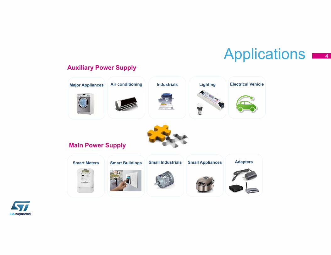
Applications 4
LightingMajor Appliances Electrical VehicleAir conditioning Industrials
Auxiliary Power Supply
Smart BuildingsSmart Meters Small AppliancesSmall Industrials Adapters
Main Power Supply
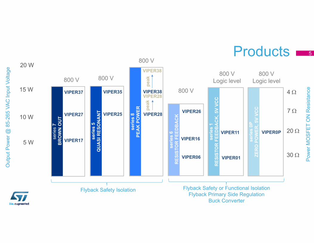
Products 5
15 W
10 W
5 W
20 W
VIPER37
serie
s 7
BR
OW
N O
UT VIPER27
VIPER17
VIPER26
serie
s 6
RES
ISTO
R F
EED
BA
CK
VIPER16
VIPER38
serie
s 8
PEA
K P
OW
ER
VIPER28
VIPER35se
ries
5Q
UA
SI R
ESO
NA
NT VIPER25
VIPER06
serie
s 1
RES
ISTO
R F
EED
BA
CK
, 5V
VCC
VIPER11
VIPER01
serie
s 0P
ZER
O P
OW
ER, 5
V VC
C
VIPER0P
Flyback Safety Isolation Flyback Safety or Functional IsolationFlyback Primary Side Regulation
Buck Converter
800 V 800 V
800 V
800 V
800 VLogic level
800 VLogic level
Out
put P
ower
@ 8
5-26
5 VA
C In
put V
olta
ge
7
20
30
4 VIPER28
VIPER38
peak
peak
Pow
er M
OS
FET
ON
Res
ista
nce
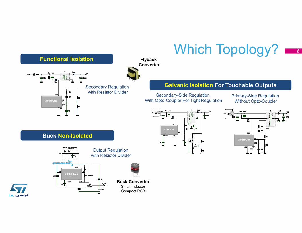
Which Topology? 6
Galvanic Isolation For Touchable OutputsSecondary-Side Regulation
With Opto-Coupler For Tight RegulationPrimary-Side Regulation
Without Opto-Coupler
Functional Isolation
Secondary Regulation with Resistor Divider
Buck Non-Isolated
Buck ConverterSmall InductorCompact PCB
Output Regulationwith Resistor Divider
FlybackConverter

Flyback Topology Optimization
Flyback Operation 8
C1
D1
C2
Q1
1 4
2 3
T1Inpu
t DC Output DC
+ +
-
-
+
+-
-IQ1
211 2
1PKQPT ILE
SWPKQPT fILP 211 2
1
On
Osc
illat
ion
Off
PKQTPKQS
PPKD InI
NNI 1111
211 2
1PKDST ILE
21T
PS n
LL
IQ1
VQ1
ID1
ON OFF ON OFFOSC
C1
D1
C2
Q1
1 4
2 3T1In
put D
C Output DC
+ +
-
-+
+-
-
ID1
IQ1
VQ1
ID1
ON OFF ON OFFOSC
C1
D1
C2
Q1
1 4
2 3
T1Inpu
t DC Output DC
+ +
-
-
IQ1
VQ1
ID1
ON OFF ON OFFOSC
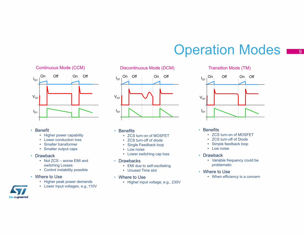
Operation Modes 9
IQ1
VQ1
ID1
On Off On Off
• Benefits• ZCS turn-on of MOSFET• ZCS turn-off of diode• Single Feedback loop• Low noise• Lower switching cap loss
• Drawbacks• EMI due to self-oscillating• Unused Time slot
• Where to Use• Higher input voltage, e.g., 230V
Discontinuous Mode (DCM)
IQ1
VQ1
ID1
On Off On Off
Transition Mode (TM)
• Benefits• ZCS turn-on of MOSFET• ZCS turn-off of Diode• Simple feedback loop• Low noise
• Drawback• Variable frequency could be
problematic
• Where to Use• When efficiency is a concern
IQ1
VQ1
ID1
On Off On Off
Continuous Mode (CCM)
• Benefit• Higher power capability• Lower conduction loss• Smaller transformer• Smaller output caps
• Drawback• Not ZCS – worse EMI and
switching Losses• Control instability possible
• Where to Use• Higher peak power demands• Lower input voltages, e.g.,110V
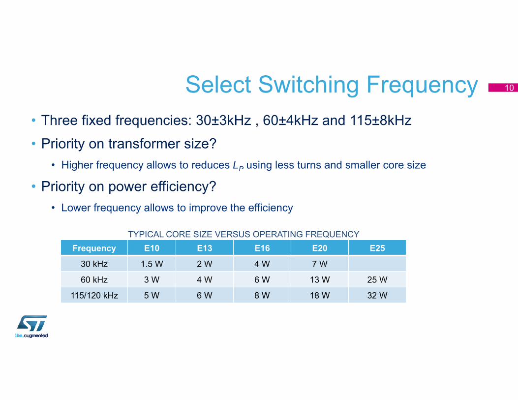
Select Switching Frequency• Three fixed frequencies: 30±3kHz , 60±4kHz and 115±8kHz
• Priority on transformer size?• Higher frequency allows to reduces LP using less turns and smaller core size
• Priority on power efficiency?• Lower frequency allows to improve the efficiency
10
TYPICAL CORE SIZE VERSUS OPERATING FREQUENCYFrequency E10 E13 E16 E20 E25
30 kHz 1.5 W 2 W 4 W 7 W
60 kHz 3 W 4 W 6 W 13 W 25 W
115/120 kHz 5 W 6 W 8 W 18 W 32 W
Transformer Design• Basic specification of transformer include
• Size, isolation barrier, reflected voltage, peak (or saturation) current, frequency, input voltage range, output voltage and output current range
• Leakage inductance influence power loss, snubber and EMI• Typical leakage inductance is 1~3% of primary inductance depending on the transformer
structure
•
• Reflected Voltage VR is the voltage reflected from secondary output to the primary of transformer
11
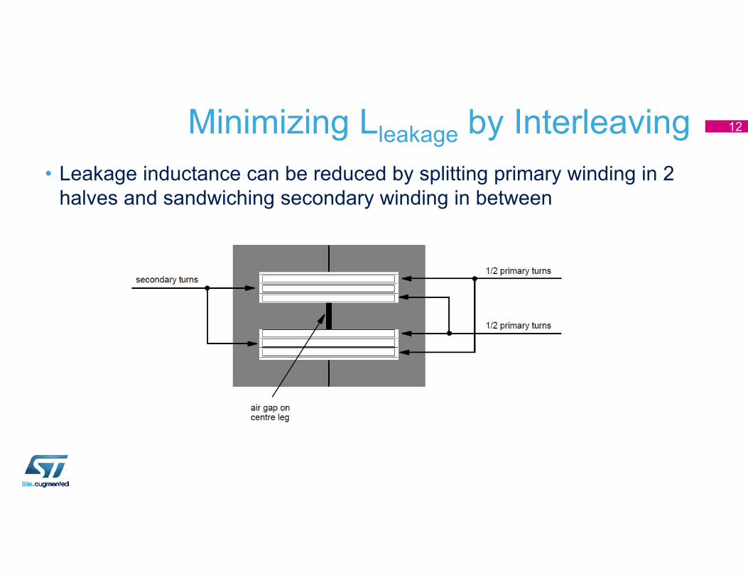
Minimizing Lleakage by Interleaving• Leakage inductance can be reduced by splitting primary winding in 2
halves and sandwiching secondary winding in between
12
Reflected Voltage Selection• Optimize reflected voltage to set maximum duty cycle. As a rule of thumb,
make it equal to minimum DC input voltage
• High reflected voltage means high Vds stress and higher snubber losses
• Lower reflected voltage means higher off time, higher RMS losses and higher primary peak current
• A positive side effect of lower reflected voltage is that it leads to better magnetic coupling between windings, which, in turn, helps to reduce leakage inductance
• On the other hand, consider that a lower reflected voltage involves higher primary peak currents at heavy load
13
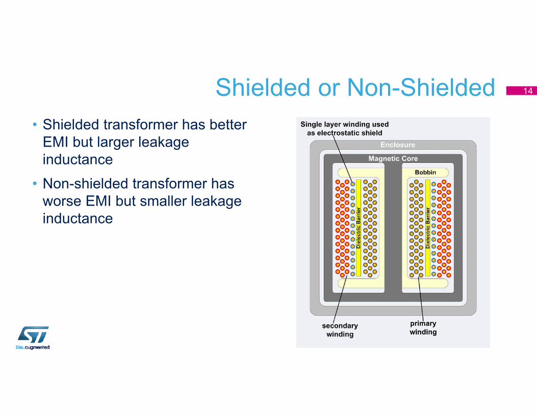
Shielded or Non-Shielded• Shielded transformer has better
EMI but larger leakage inductance
• Non-shielded transformer has worse EMI but smaller leakage inductance
14
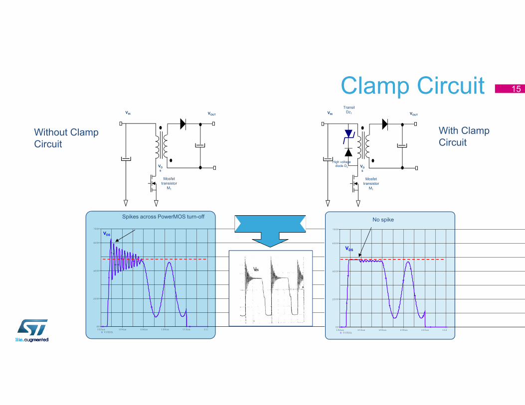
Clamp Circuit 15
No spike Spikes across PowerMOS turn-off
VIN VOUT
Mosfet transistor
M1
Transil Dz1
High voltage diode D2 VD
S
102us 104us 106us 108us 110us 112V(VDS)
0V
200V
400V
600V
700V
VDS
102us 104us 106us 108us 110us 112V(VDS)
0V
200V
400V
600V
700V
VDS
VIN VOUT
Mosfet transistor
M1
VDS
Without Clamp Circuit
With Clamp Circuit
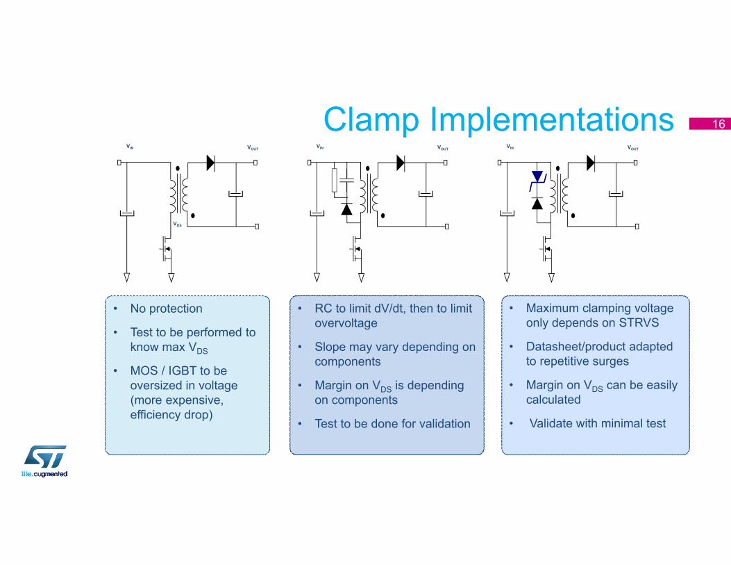
Clamp Implementations 16
• No protection
• Test to be performed to know max VDS
• MOS / IGBT to be oversized in voltage (more expensive, efficiency drop)
VIN VOUTVIN VOUT
VDS
VIN VOUT
• RC to limit dV/dt, then to limit overvoltage
• Slope may vary depending on components
• Margin on VDS is depending on components
• Test to be done for validation
• Maximum clamping voltage only depends on STRVS
• Datasheet/product adapted to repetitive surges
• Margin on VDS can be easily calculated
• Validate with minimal test
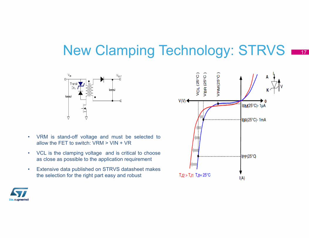
New Clamping Technology: STRVS 17
• VRM is stand-off voltage and must be selected toallow the FET to switch: VRM > VIN + VR
• VCL is the clamping voltage and is critical to chooseas close as possible to the application requirement
• Extensive data published on STRVS datasheet makesthe selection for the right part easy and robust
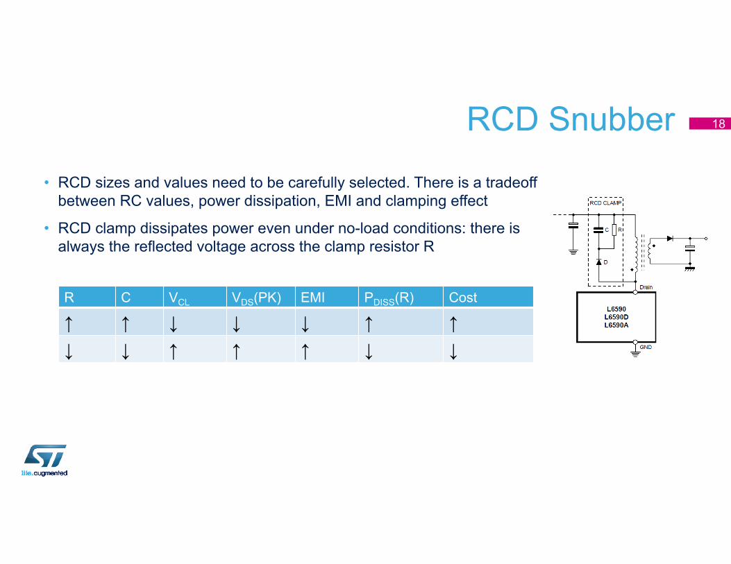
RCD Snubber
• RCD sizes and values need to be carefully selected. There is a tradeoff between RC values, power dissipation, EMI and clamping effect
• RCD clamp dissipates power even under no-load conditions: there is always the reflected voltage across the clamp resistor R
18
R C VCL VDS(PK) EMI PDISS(R) Cost
↑ ↑ ↓ ↓ ↓ ↑ ↑↓ ↓ ↑ ↑ ↑ ↓ ↓
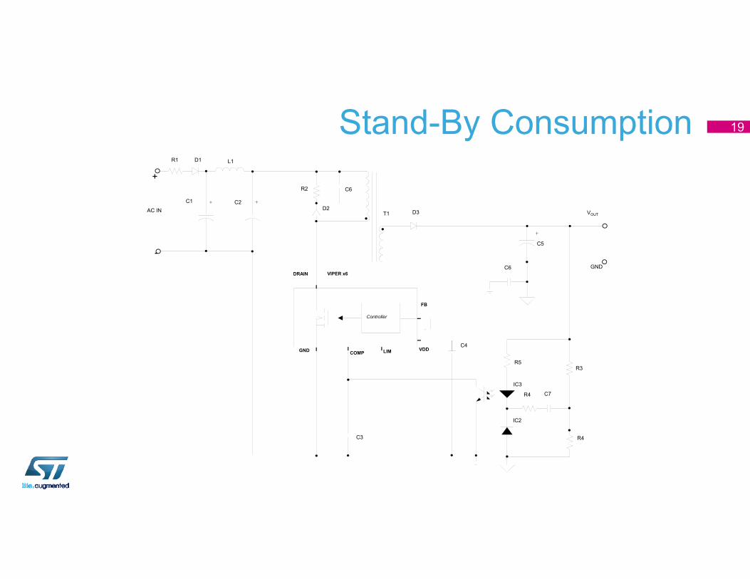
Stand-By Consumption 19
IC3
R4
R4
IC2
C7
R3
C6R2
+C1
C3
C4
+
C5
D3
L1
FB
DRAIN
GND VDDCOMP LIM
VIPER x6
D2
D1
GND
+C2
R1
AC IN VOUT
Controller
T1
+
-
R5
C6
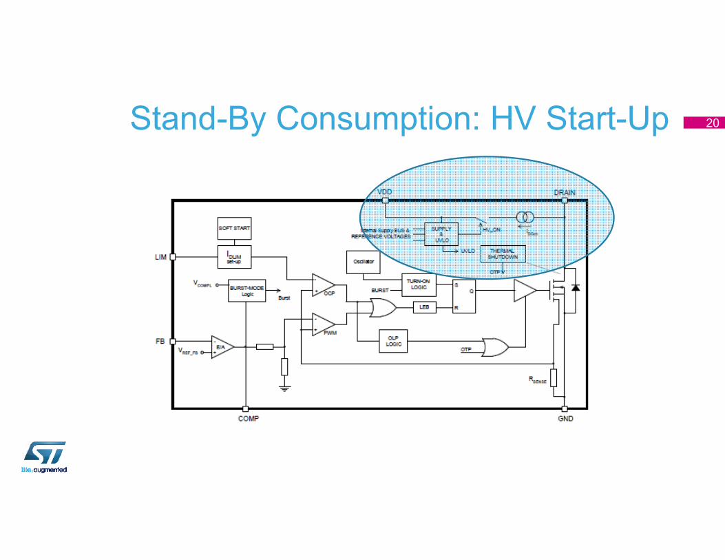
Stand-By Consumption: HV Start-Up 20
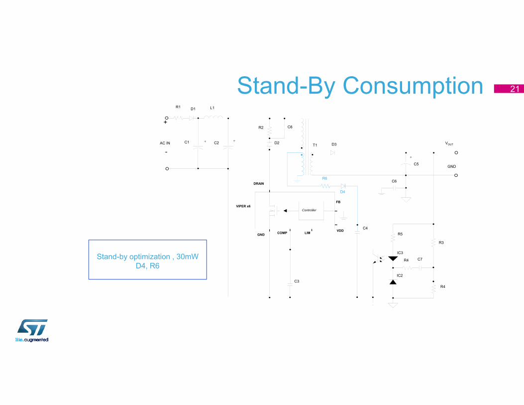
Stand-By Consumption 21
IC3
R4
R4
IC2
C7
R3
C6R2
+C1
C3
C4
+
C5
D3
L1
FB
DRAIN
GNDVDDCOMP LIM
VIPER x6
D2
D1
GND
+C2
R1
AC IN VOUT
Controller
T1
D4
R6
+
-
R5
C6
Stand-by optimization , 30mWD4, R6
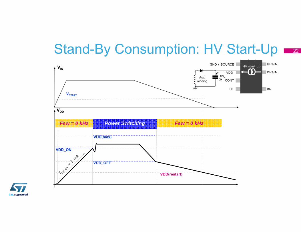
Stand-By Consumption: HV Start-Up 22
GND / SOURCE DRAIN
FB
DRAIN
CONT
VDD
BR
Auxwinding
IDS_CH
HV start up
VDD_ON
Power Switching
VDD(max)
VDD_OFF
VDD(restart)
Fsw = 0 kHz Fsw = 0 kHz
VSTART
VIN
VDD
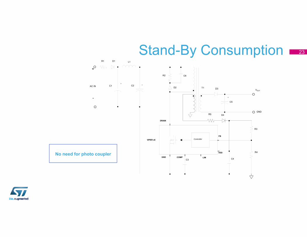
Stand-By Consumption 23
C6
R4
R2
+C1
C3 C4
R3
+
C5
D3
L1
FB
DRAIN
GND
VDD
COMP LIM
VIPER x6
D2
D1
GND
+C2
R1
AC INVOUT
Controller
T1
D4R5
+
-
No need for photo coupler
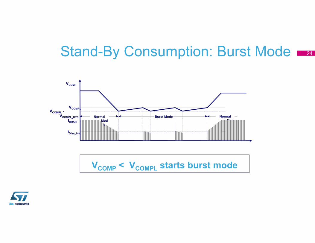
Stand-By Consumption: Burst Mode 24
VCOMPLVCOMPL -
VCOMPL_HYSIDRAIN
Normal Mod
e
Burst Mode Normal Mod
e
VCOMP
IDlim_bm
VCOMP < VCOMPL starts burst mode
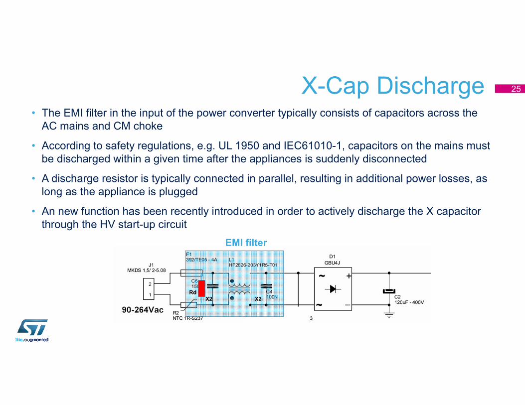
X-Cap Discharge• The EMI filter in the input of the power converter typically consists of capacitors across the
AC mains and CM choke
• According to safety regulations, e.g. UL 1950 and IEC61010-1, capacitors on the mains must be discharged within a given time after the appliances is suddenly disconnected
• A discharge resistor is typically connected in parallel, resulting in additional power losses, as long as the appliance is plugged
• An new function has been recently introduced in order to actively discharge the X capacitor through the HV start-up circuit
25
EMI filter
X2 X2Rd

Buck Topology Optimization
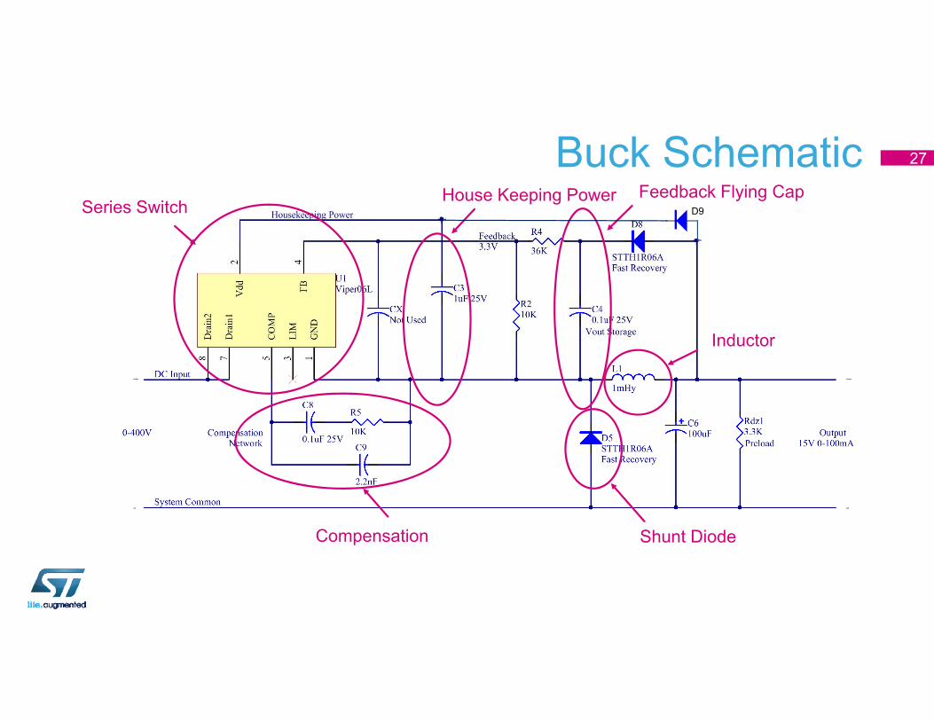
Buck Schematic 27
Feedback Flying CapSeries Switch
Shunt Diode
Inductor
House Keeping Power
Compensation
D9

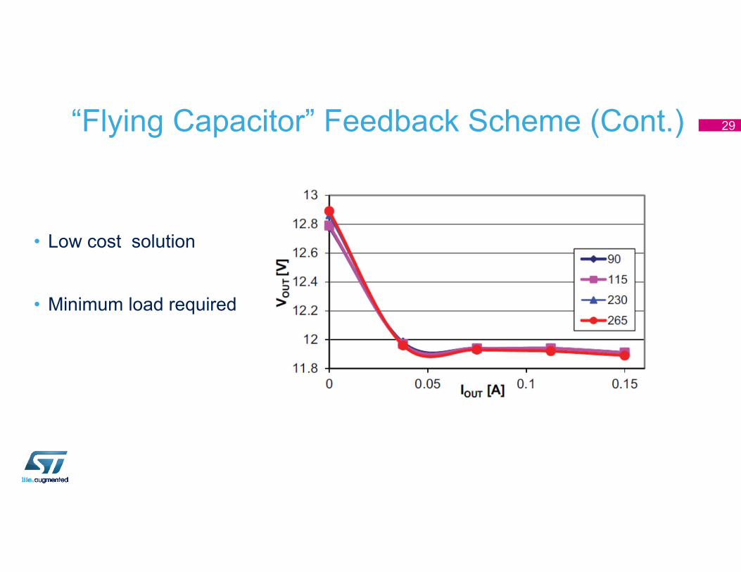
“Flying Capacitor” Feedback Scheme• C4 stores output voltage, transfers level into Viper feedback loop
• R4 – R2 discharge C4 slowly
• Load current is required to turn on D5 and D8 to charge C4
• A light load MUST be present to insure diode turn-on
• C4 must hold output voltage information when Viper is in burst mode
28
“Flying Capacitor” Feedback Scheme (Cont.)
• Low cost solution
• Minimum load required
29

Select Switching Frequency 30
SELECT FREQUENCY FOR 5 V OUTPUT BUCK
Vin DC (V) D (%) 5 V tON (μs) for 60 kHz 5 V
tON (μs) for 30 kHz 5 V
VIPer01 Minimum ON
time100 (85 VAC) 5.0 0.83 1.67
0.35 μs170V (120 VAC) 2.9 0.49 0.97
325V (230 VAC) 1.5 0.26 0.50
375V (265 VAC) 1.3 0.22 0.33
622V (440 VAC) 0.8 0.13 0.26
Lower frequency allows to handle the regulation even in the case of a very high ratio between input and output voltages
Minimum ON Time 31
• Duty cycle of Viper Buck converter is limited by minimum on time• Viper06 450 ns • Viper01 350 ns
• If the required ON time is shorter then minimum ON time, Buck still works, but there is small instability and the maximum deliverable output current is reduced.
• The 30kHz version is strictly recommended for 5V output
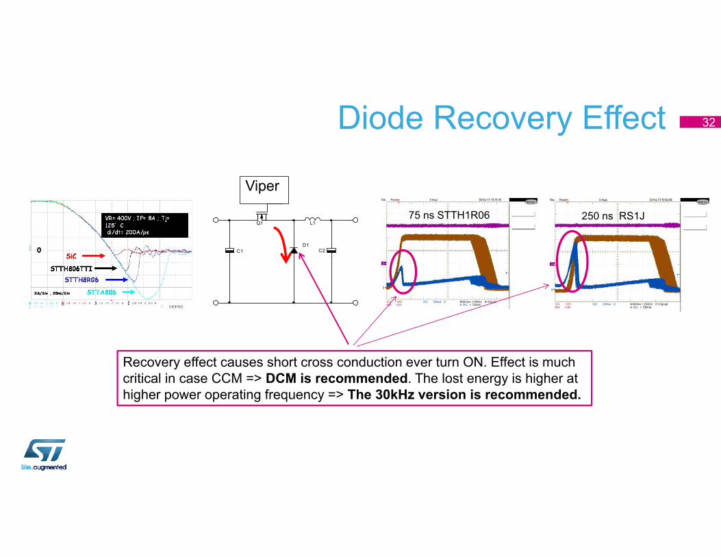
Diode Recovery Effect 32
Recovery effect causes short cross conduction ever turn ON. Effect is much critical in case CCM => DCM is recommended. The lost energy is higher at higher power operating frequency => The 30kHz version is recommended.
Viper
L1
C1D1
C2
Q175 ns STTH1R06 250 ns RS1J
Layout and EMI Optimization
Layout Optimization• Minimize interconnection lengths of following components:
• Input filter caps, input-side transformer (or inductor), power MOSFET, sensing resistors and active-clamp or snubber circuits
• Output-side transformer (or inductor), rectifier diodes and output filter caps
• Keep power and signal circuitries separated and careful of connection between the signal and power grounds
• Assure component isolation and spacing by safety standards
• Prioritize ground over all routes
• Compromise copper areas between Thermal and EMI
• Add sufficient VIAs for better thermal performance
• Keep the feedback path as far as possible from power components and noise traces
• External compensation components should be close to IC
• Copper traces for power should be thick and short and sharp angles should be avoided
34
EMI Optimization• EN 55022 is an European EMC standard applicable to information technology equipment with a rated supply voltage
not exceeding 600 V
• Properly size EMI filter: differential mode filter for power < 5 W; X-, Y-caps, and common mode choke for power > 15 W
• Designers often use snubbers and soft switching techniques to minimize the EMI
• Shielded transformer has better EMI but also has larger leakage inductance
• Connect heatsinks to ground
• Focus on coupling paths from EMI sources to EMI sensitive components
• Strategic orientation and placement of components can reduce EMI generation significantly
• Eliminate environmental interference on EMI test
• Use an accurate EMI analyzer to carry quasi-peak, and average measurement to meet standards
• ST offers PWM operation with frequency jittering for low EMI
35
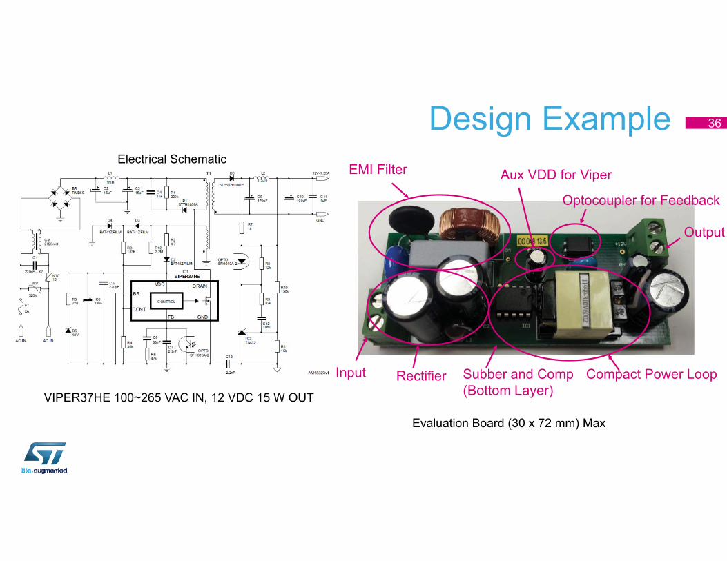
Design Example 36
VIPER37HE 100~265 VAC IN, 12 VDC 15 W OUT
Electrical Schematic
Evaluation Board (30 x 72 mm) Max
Compact Power Loop
Optocoupler for Feedback
Output
EMI Filter
Rectifier Subber and Comp(Bottom Layer)
Aux VDD for Viper
Input
eDesignSuite Examples
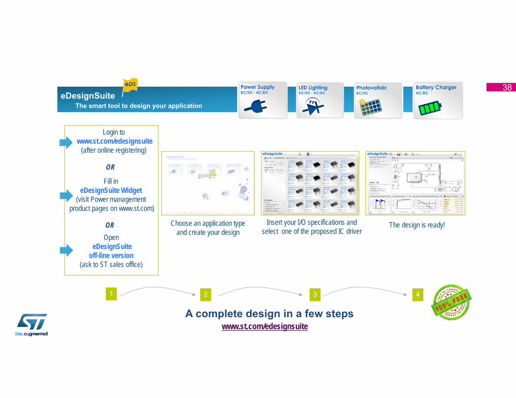
38
Choose an application type and create your design
The design is ready!Insert your I/O specifications and select one of the proposed IC driver
The smart tool to design your applicationeDesignSuite
2 3 41
A complete design in a few steps
Login towww.st.com/edesignsuite
(after online registering)
OpeneDesignSuite
off-line version(ask to ST sales office)
OR
Fill ineDesignSuite Widget
(visit Power managementproduct pages on www.st.com)
OR
www.st.com/edesignsuite
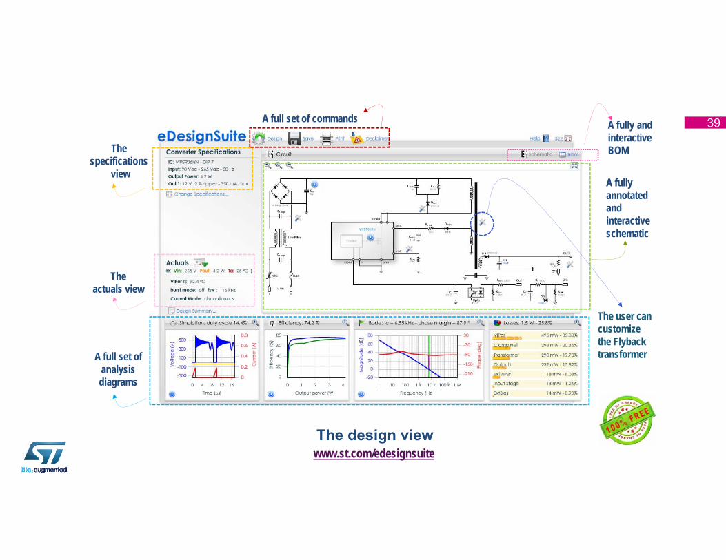
39
The specifications
view
The actuals view
A full set of analysis diagrams
A fully annotatedandinteractive schematic
A fully and interactive BOM
A full set of commands
The user can customize the Flybacktransformer
The design viewwww.st.com/edesignsuite

40