abstract document: ultra small antenna and low power receiver
TRANSCRIPT

ABSTRACT Title of Document: ULTRA SMALL ANTENNA AND LOW
POWER RECEIVER FOR SMART DUST WIRELESS SENSOR NETWORKS
Bo Yang
Doctor of Philosophy, 2009 Directed By: Professor Neil Goldsman
Department of Electrical and Computer Engineering
Wireless Sensor Networks have the potential for profound impact on our daily
lives. Smart Dust Wireless Sensor Networks (SDWSNs) are emerging members of
the Wireless Sensor Network family with strict requirements on communication node
sizes (1cm3) and power consumption (< 2mW during short on-states). In addition, the
large number of communication nodes needed in SDWSN require highly integrated
solutions. This dissertation develops new design techniques for low-volume antennas
and low-power receivers for SDWSN applications. In addition, it devises an antenna
and low noise amplifier co-design methodology to increase the level of design
integration, reduce receiver noise, and reduce the development cycle.
This dissertation first establishes stringent principles for designing SDWSN
electrically small antennas (ESAs). Based on these principles, a new ESA, the F-
Inverted Compact Antenna (FICA), is designed at 916MHz. This FICA has a

significant advantage in that it uses a small-size ground plane. The volume of this
FICA (including the ground plane) is only 7% of other state-of-the-art ESAs, while its
efficiency (48.53%) and gain (-1.38dBi) are comparable to antennas of much larger
dimensions. A physics-based circuit model is developed for this FICA to assist
system level design at the earliest stage, including optimization of the antenna
performance. An antenna and low noise amplifier (LNA) co-design method is
proposed and proven to be valid to design low power LNAs with the very low noise
figure of only 1.5dB.
To reduce receiver power consumption, this dissertation proposes a novel
LNA active device and an input/ouput passive matching network optimization
method. With this method, a power efficient high voltage gain cascode LNA was
designed in a 0.13µm CMOS process with only low quality factor inductors. This
LNA has a 3.6dB noise figure, voltage gain of 24dB, input third intercept point (IIP3)
of 3dBm, and power consumption of 1.5mW at 1.0V supply voltage. Its figure of
merit, using the typical definition, is twice that of the best in the literature. A full low
power receiver is developed with a sensitivity of -58dBm, chip area of 1.1mm2, and
power consumption of 2.85mW.

ULTRA SMALL ANTENNA AND LOW POWER RECEIVER FOR SMART DUST WIRELESS SENSOR NETWORKS
By
Bo Yang
Dissertation submitted to the Faculty of the Graduate School of the University of Maryland, College Park, in partial fulfillment
of the requirements for the degree of Doctor of Philosophy
2009
Advisory Committee: Professor Neil Goldsman, Chair/Advisor Dr. Quirino Balzano Professor Martin C. Peckerar Professor Shuvra S. Bhattacharyya Professor Ellen Williams

© Copyright by Bo Yang
2009

ii
Acknowledgements
It is a pleasure to thank those who made this dissertation possible.
First and foremost, I am heartily thankful to my advisor, Prof. Neil Goldsman,
for the great opportunity he offered me to work with him and for guiding me through
the research. His vision for this interdisciplinary cutting-edge technology, his
encouragement, his support, and his supervision had led me through the entire
research project. It would have been next to impossible to write this dissertation
without his help and guidance. In addition, his enthusiasm for his career will
continuously inspire me in the rest of my life. I am truly grateful to Dr. Quirino
Balzano, my co-advisor, whose broad vision and industry experience in wireless
portable devices, guidance, and pleasant personality have made this research
experience both rewarding and joyful. What I learned from him has not only been
about research, but also about professional life. I would also like to thank Prof.
Martin Peckerar, who was a committee member at my Master’s defense and doctoral
proposal exam, as well as the instructor of my analog circuit and device physics
courses. His passion for both research and educating students and junior researchers
will have an impact in my future career. My appreciation also goes to Prof. Shuvra
Bhattacharyya, who was a committee member at my dissertation proposal exam. I
would also like to thank Prof. Ellen Williams for kindly consenting to join the
defense committee and review this dissertation.
I have been fortunate to collaborate with many brilliant and supportive people
through the years. In particular, I would like to thank Dr. Xi Shao for his valuable
discussions on antenna and electromagnetic problems. I also thank Dr. Thomas Salter,

iii
Dr. Todd Firestone, and Mr. Donald M. Witters, Jr., for providing testing instruments.
I have appreciated the co-operation with several Smart Dust project team members:
Dr. Zynep Dilli, Mr. Bo Li, Dr. Thomas Salter, Dr. Chung-Ching Shen, Ms. Datta
Sheth, Dr. Felice Vanin, Mr. Shaun Simmons, and Ms. Yiming Zhai. I also thank
Prof. Pamela Abshire, Dr. Akin Akturk, Dr. Siddarth Potbhare, Prof. Ohmar Ramahi,
Dr. John Rodgers, and Dr. Bai Yun for very profitable discussions. My appreciation
also goes to Mr. Jay Renner, Mr. Shyam Mehrotra, Mr. Bryan Quinn, Mr. Joe
Kselman, and Mr. Jay Pyle for technical support.
Next, I would like to thank my family. I thank my parents for providing me
the best education that I could ever have and teaching me be optimistic during
difficult times. I want to thank my husband, Tao, for his love and encouragement
from college times onward.
Lastly, I offer my regards and blessings to all of those who supported me in
any respect during the completion of this project.

iv
Table of Contents Acknowledgements....................................................................................................... ii Table of Contents......................................................................................................... iv List of Tables ............................................................................................................... vi List of Figures ............................................................................................................. vii Chapter 1 Introduction .................................................................................................. 1
1.1 Motivation........................................................................................................... 1 1.2 Contributions....................................................................................................... 2 1.3 Thesis Structure .................................................................................................. 7
Chapter 2 Design Philosophy for Smart Dust Wireless Sensor Networks (SDWSN).. 9 2.1 Smart Dust Wireless Sensor Networks (SDWSN) ........................................... 10
2.1.1 The Concepts of WSN and SDWSN ......................................................... 10 2.1.2 Smart Dust Requirements .......................................................................... 11
2.2 Design Challenges ............................................................................................ 12 2.2.1 Low Power ................................................................................................. 13 2.2.2 Low Cost .................................................................................................... 13 2.2.3 Low Form Factor ....................................................................................... 14
2.3 Design Trade-Offs ............................................................................................ 14 2.4 State of the Art .................................................................................................. 17
2.4.1 Direct Conversion Receiver ....................................................................... 17 2.4.2 Low IF Receiver ........................................................................................ 19 2.4.3 Super-Regenerative Receiver..................................................................... 20 2.4.4 Proposed Receiver Architecture: Direct Demodulation Receiver (DDR) . 22
2.5 Receiver Design Goals...................................................................................... 23 2.5.1 Sensitivity Requirements ........................................................................... 24 2.5.2 Receiver Budget......................................................................................... 27
2.6 Conclusion ........................................................................................................ 28 Chapter 3 Scalable Highly Efficient Electrically Small Antennas (ESA) .................. 29
3.1 ESA State of the Art ......................................................................................... 30 3.2 The Need for ESA in Smart Dust System......................................................... 37 3.3 Design Guidelines for ESAs ............................................................................. 39
3.3.1 Antenna Height .......................................................................................... 39 3.3.2 Antenna Loss ............................................................................................. 40 3.3.3 Antenna Volume ........................................................................................ 41
3.4 Innovative ESAs: F-Inverted Compact Antennas (FICAs) .............................. 42 3.4.1 Design Origins ........................................................................................... 43 3.4.2 Innovative ESAs ........................................................................................ 45 3.4.3 Principle of Operation................................................................................ 50 3.4.4 Using Baluns in ESA Tests........................................................................ 53 3.4.5 Simulation and Measurements................................................................... 55 3.4.6 Antenna on a Live Radio ........................................................................... 64 3.4.7 FICA Parametric Study.............................................................................. 66
3.5 Ground Plane Effect for ESA and FICA........................................................... 71

v
3.6 FICA Circuit Model.......................................................................................... 73 3.7 Scaling FICA to Other Frequencies.................................................................. 80 3.8 Conclusion ........................................................................................................ 83
Chapter 4 Low Power Low Noise Amplifier Optimization........................................ 85 4.1 Introduction....................................................................................................... 86
4.1.1 Existing LNA Design and Optimization Methods..................................... 86 4.1.2 Cascode LNA Design Space Exploration .................................................. 88
4.2 Optimizing Low Power LNA Sizing and Biasing ............................................ 90 4.2.1 Cascode LNA Transistor Optimization Modeling..................................... 90 4.2.2 Systematic Investigation of Transistor Sizing and Biasing ....................... 95
4.3 Optimizing Matching Networks ..................................................................... 103 4.3.1 Voltage Gain Oriented Design................................................................. 103 4.3.2 Voltage Gain and Noise Figure Trade-Offs............................................. 107
4.4 Optimizing Input Matching Networks ............................................................ 110 4.4.1 Input Matching Network Design Guideline for Unilateral Circuits ........ 110 4.4.2 Input Matching Network Design Guideline for Bilateral Circuits........... 113
4.5 Optimizing Output Matching Circuit.............................................................. 120 4.6 A 2.2GHz LNA Design Example ................................................................... 121 4.7 Conclusion ...................................................................................................... 126
Chapter 5 Antenna and Low Noise Amplifier (LNA) Co-Design............................ 127 5.1 Introduction..................................................................................................... 128 5.2 FICA Circuit Model........................................................................................ 130 5.3 Optimum Noise Matching Using Antenna-LNA Co-Design.......................... 132 5.4 Conclusion ...................................................................................................... 137
Chapter 6 Low Power Receiver for Smart Dust Wireless Sensor Networks............ 138 6.1 Introduction..................................................................................................... 139 6.2 Receiver Circuitry........................................................................................... 142
6.2.1 Demodulator ............................................................................................ 143 6.2.2 Auxiliary Amplifier ................................................................................. 155 6.2.3 Comparator .............................................................................................. 158
6.3 Layout and Experimental Results ................................................................... 162 6.4 Transceiver Design and Results...................................................................... 173 6.5 Conclusion ...................................................................................................... 178
Chapter 7 Summary and Future Work..................................................................... 180 7.1 Research Summary ......................................................................................... 180 7.2 Future Work .................................................................................................... 182
7.2.1 Radio Units for SDWSN at Tens of GHz ................................................ 182 7.2.2 System Integration ................................................................................... 183 7.2.3 New SDWSN Radio with Advanced Technology................................... 183
Appendix A............................................................................................................... 184 Appendix B ............................................................................................................... 186 Bibliography ............................................................................................................. 191

vi
List of Tables
Table 1.1 Antenna performance summary (NA=Not Available)……….……….3 Table 1.2 Literature results shown in Fig. 1.1 and Fig. 1.2……………….….…5 Table 1.3 Summary of receiver performance…………………………….….…..7 Table 2.1 Wireless personal area network (WPAN) IEEE standards……….….10 Table 2.2 Path loss (dB) for 2.2GHz SDWSN communication…………...…....25 Table 3.1 Antenna performance summary (NA=Not Available)……………….64 Table 3.2 Variables used in parametric simulation……………………………..67 Table 3.3 Resonance frequency (fc) of FICA for different h1, d1, θ, and φ…....68 Table 3.4 Values used in coil parametric study………………………………...69 Table 3.5 Gain of chip antenna assembled on different PCBs…………….……73 Table 3.6 Measured FICA input impedance at resonance……………………...77 Table 4.1 Literature results shown in Fig. 4.28……………………………….125 Table 6.1 Simulation parameters used in Fig. 6.4………………………..……146 Table 6.2 Component values used in Fig. 6.12……………………………..…156 Table 6.3 Comparator types and characteristics……………………………....159 Table 6.4 Sizes of transistors in Fig. 6.16………………………………..……162 Table 6.5 Summary of receiver performance…………………………….……173 Table 6.6 Component parameters in Fig. 6.25. (W/L in µm/µm)……….…….176 Table 6.7 Transceiver operation status vs. control bits………………….…….176

vii
List of Figures
Fig. 1.1 FoM of LNAs. References in this figure can be found in Table. 1.2…...…4 Fig. 1.2 FoM (FoM2 = (Gain • f) / (F - 1) / Pdc) of LNAs. References in this
figure can be found in Table. 1.2. …………………………………….6 Fig. 2.1 SDWSN design tradeoffs………………………………………….….….15 Fig. 2.2 Block diagram of a direct conversion receiver……….……………….…18 Fig. 2.3 Block diagram of low-IF receiver………………………………………..20 Fig. 2.4 Block diagram of super-regenerative receiver [Otis05]……………….…21 Fig. 2.5 Block diagram of direct demodulation receiver (DDR) for OOK….……23 Fig. 2.6 Sensitivity of receiver vs. communication distance d and modification
index n. Left: transmitter dissipates 1mW. With 40% efficiency, effectively transmitted power is 0.4mW. Right: transmitter dissipates 2mW. With 40% efficiency, effectively transmitted power is 0.8mW…..26
Fig. 2.7 OOK receiver block diagram with gain and noise estimations……..……27 Fig. 3.1 Printed dipole antennas: (a) printed dipole antennas on PCB [Chuang03],
(b) printed dipole on silicon substrates [Lin04]…………………….……31 Fig. 3.2 Rectangular dielectric resonance antenna placed on a ground plane
[Mongia97]. ………………………………………………………..……32 Fig. 3.3 Microstrip patch antennas……………………………………………..…33 Fig. 3.4 Diagram of an inverted-F antenna (IFA)……………………...…………34 Fig. 3.5 Planar Inverted-F antennas (PIFA) (left) [Boyle06] and meander line PIFA
(right) [Pham04]………………………………………………………….35 Fig. 3.6 Genetic algorithm antennas [Choo05]. Left: theoretical design. Right:
photo of implemented antenna…………………………………...………36 Fig. 3.7 A spiral antenna with electromagnetic band-gap (EBG) structures
[Bell04]…………………………………………………………………..37 Fig. 3.8 Operation principles of folded dipole antennas……………………….…43 Fig. 3.9 Measured S11 of the wired meander line with no dielectric loading. The
antenna is made with 1mm diameter copper wires. The antenna height is
8mm (0.024λ). The ground plane is 25mm × 40mm (0.076λ × 0.122λ at 916MHz). The bandwidth is 40MHz, about 4.4% at 916MHz. ………...46
Fig. 3.10 Top view (a) and side view (b) of the dielectric loaded FICA antenna. The
size of the ground plane is 20mm × 25mm (0.06λ × 0.08λ at 916MHz). The height of the antenna is 7mm. The dielectric load is a Teflon block
with size 10mm × 10mm × 6mm, and a relative dielectric constant of 2.2……………………………………………………………………….47
Fig. 3.11 Measured S11 of the wired FICA with Teflon dielectric loading. The geometry of the FICA is shown in detail in Fig. 3.10. The bandwidth is 15MHz at -10dB, which is around 1.6% at 916MHz……………..…….48
Fig. 3.12 Photographs of (a) side view and (b) top view of the 916MHz FICA. The
total volume (including ground plane) is 8mm × 20mm × 25mm (0.06λ ×
0.076λ × 0.024λ)…………………………………………………….….50 Fig. 3.13 Mesh plot of FICA in HFSS simulation..…………………………….…51

viii
Fig. 3.14 Current density distribution on FICA wires……………………….……52 Fig. 3.15 Near field measurement construction………………………………..…..54 Fig. 3.16 Top: Near electric field measurement results of antennas fed by different
cables. (a) Field measured with choked cable. (b) Field measured with a simple coaxial cable without RF chokes. Bottom: Photo of AUT fed by choked cable…………………………………………………………..…55
Fig. 3.17 Simulated and measured S11 of the FICA. Simulation: center frequency is 915MHz; -3dB bandwidth is 16.8MHz. Measurement: center frequency is 915.2MHz; -3dB bandwidth is 22.4MHz. Embedded plot: models used in
HFSS. Pin1: feeding pin. Pin2: shorting pin. Ground plane size: 20mm × 2 5 m m … … … … … … … … … … … … … … … … … … . . … . 5 6
Fig. 3.18 Experimental settings for radiation pattern test. (a) Diagram of the setting. (b) Setting in an open field. (c) Setting inside an anechoic chamber.….58
Fig. 3.19 (a) Eφ and Eθ defined in the FICA XY plane. (b) Measured and simulated radiation pattern (gain) of the antenna on the XY plane………………..60
Fig. 3.20 Image current. (a) Image current of vertical and horizontal electrical current over a ground plane. (b) Image current of electrical current on a small loop over a ground plane…………………………………….…..62
Fig. 3.21 Electrical current and its image current along the helix of FICA……....63 Fig. 3.22 Sensor node used in field measurements…………………………….…65 Fig. 3.23 Geometric representation of some analyzed parameters…………….…67 Fig. 3.24 Simulated S11 with different spacing s. AD and N are adjusted
simultaneously such that the length of the wire from the tapping point to the open end is roughly constant. Other parameters in the analysis have the default values in Table 3.2………………………………………….…. 70
Fig. 3.25 Simulated S11 with different major diameters for the coil and s = 2mm. AD and N are adjusted simultaneously such that the length of the wire from the tapping point to the open end is roughly constant. Other parameters in the analysis have the default values in Table 3.2…………71
Fig. 3.26 Commercial 916MHz chip antenna assembled on PCBs of different sizes. From left to right: Chip antenna on PCB1; Chip antenna on PCB2; Chip antenna on PCB3………………………………………………………...73
Fig. 3.27 FICA circuit. (a) Photo of FICA; (b) circuit model of FICA; (c) equivalent circuit of (b)……………………………………………………………...75
Fig. 3.28 Measured Zin and modeled Zin. Ground plane size: 20mm × 25mm…79
Fig. 3.29 Measured Zin and modeled Zin. Ground plane size: left: 60mm × 75mm;
right: 76.2mm × 95.3mm………………………………………………80 Fig. 3.30 Diagram (a) and photograph (b) of FICA at 2.2GHz and 2.45GHz…...81 Fig. 3.31 Measured gain of a 2.2GHz FICA. Left: Eφ and Eθ on XY plane. Right: Eφ
and Eθ on XZ plane. Coordinates are defined in Fig. 3.19 and Fig. 3.30.82 Fig. 3.32 Measured S11 of FICA scaled to 433MHz……………………….……..83 Fig. 4.1 Design flow of low noise amplifier (LNA)………………………………90 Fig. 4.2 (a) gm/ID - IC plot for 0.13µm CMOS. (b) VGS - IC plot for 0.13µm
CMOS……………………………………………………….…………..93

ix
Fig. 4.3 Normalized obj(VGS,W) versus bias VGS(V) and transistor width W(µm). (a) Analytical model (4.8 b). (b) Cadence simulation…………….……..…..94
Fig. 4.4 Design flow for transistor biasing and sizing in Cadence simulation. Intrinsic Gain Efficiency: IGE = gm1(gm2ro1ro2 + ro1 + ro2) / ID. Intrinsic Gain: IG = gm1(gm2ro1ro2 + ro1 + ro2)………………………….…………95
Fig. 4.5 Cascode transistor intrinsic gain efficiency vs W at different gate biasing levels…………………………………………………………….……….96
Fig. 4.6 NF, NFmin, and Rn vs. W for cascode transistors. Top: weak inversion region. Middle: moderate inversion region. Bottom: moderate inversion region with higher VG1………………………………………………99
Fig. 4.7 (a) Intrinsic gain efficiency (IGE) and (b) intrinsic gain (IG) of cascode transistors vs. VG1 at different supply voltage levels. Transistor sizes are W/L = 100/0.12µm……………….………………………………….100
Fig. 4.8 Noise characteristics vs. VG1 at different supply voltage levels. Transistor sizes are W/L = 100/0.12µm. Top: minimum achievable noise figure NFmin. Middle: noise sensitivity factor Rn. Bottom: overall noise figure NF…………………………………………………………………..…..102
Fig. 4.9 NFmin, NF, and Rn vs. transistor finger width. Transistor sizes are W/L = 120/0.12µm. Biasing condition is VG1 = 0.46V. Supply voltage is 1.2V……………………………………………………………….…….103
Fig. 4.10 LNA cascaded with common source stage and current source load. LNAs (a): designed for maximum power gain, (b): for maximum voltage gain...........................................................................................................105
Fig. 4.11 Simulated power gain and voltage gain of LNAs designed for high power gain or high voltage gain. The difference of RF input in LNAs (a) and (b) is because the RF input is the AC voltage from the gate of M1 to the ground, not from port1 to ground. Due to the capacitive voltage amplification (section 4.4.1), these voltages differ slightly…………….106
Fig. 4.12 Two-port network for noise analysis………………………………...…108 Fig. 4.13 (a) NF and NFmin for Rload = 10Ω to 1MΩ. Curves for different Rload
values collapse into one NF and one NFmin plot. (b) S22(dB) for different values of Rload. Since we only demonstrate the insensitivity of NF to Rload, the particular Rload value for each curve in panel (b) is not important, and these are not labeled due to space limitations…………..110
Fig. 4.14 LC series circuit for LNA input matching network………………….…111 Fig. 4.15 Input impedance calculation for a Cascode LNA with LC tank load. Cx =
Cgb1 + Cgs2 + Cbs2, Cy = Cgd2 + Cdb2 + CL..……………………....113 Fig. 4.16 Small signal model for cascode LNA…………………………………..114 Fig. 4.17 Primary panels: Cadence simulation results for real and imaginary parts of
Zx in Fig. 4.16. Insets: Analytical model (4.23) of real and imaginary parts of Zx in Fig. 4.16………………………………………………………..115
Fig. 4.18 Small signal circuit for input impedance calculation of cascode LNA...115 Fig. 4.19 Input impedance of cascode LNA with lossy LC resonance tank. Primary
panels: real and imaginary Zin from Cadence simulation. Insets: analytical results according to (4.24)………………………………………………117
Fig. 4.20 Cascode LNA with source degeneration………………………………..119

x
Fig. 4.21 Input impedance of Cascode LNA with Ls. Primary panels: real and imaginary parts of Zin from Cadence simulation. Insets: real and imaginary parts of Zin according to (4.28)…………………………….120
Fig. 4.22 Simplified 2.2GHz LNA schematic………………………………..….121 Fig. 4.23 Layout and die microphoto of 2.2GHz LNA using 0.13µm IBM8RFLM
technology………………………………………………………………122 Fig. 4.24 Measured LNA S-parameters…………………………………………..122 Fig. 4.25 Measured LNA P-1dB point……………………………………..……..123 Fig. 4.26 (a) Simulated and (b) measured noise figure for the LNA………….….123 Fig. 4.27 IIP3 measurement for LNA biased at different levels. (a): VDD = 1.2V,
IIP3 = 5dBm. (b): VDD = 1.0V, IIP3 = 3dBm…………………….….124 Fig. 4.28 FoM of LNA computed (a) using (4.29), (b) using (4.30)……………...125 Fig. 5.1 Simplified cascode LNA topology……………………………………...128 Fig. 5.2 Simulated (Cadence) gains and noise figures for a LNA with different
inductor quality factors…………………………………………………129 Fig. 5.3 FICA model for (a and b) transmitter, (c) receiver, and (d) observed
results…………………………………………………………………...131 Fig. 5.4 Antenna and LNA co-design………………………………………...…134 Fig. 5.5 Simulated antenna and LNA co-design result. Left: NF and NFmin. Right:
Rn………………………………………………………………………135 Fig. 5.6 Simulated S parameter for antenna and LNA co-design in Fig. 5.4. Dotted
line: S21. Dashed line: S11. Solid line: S22……………………………136 Fig. 5.7 FoM (FoM = (Gain • f) / (F - 1) / Pdc) of LNAs. References in this figure
can be found in Table. 1.2. ………………………………………....137 Fig. 6.1 Inverter amplifier using current reusing technique for higher gain and
lower power consumption………………………………………………141 Fig. 6.2 Demodulations of envelope detector in a direct demodulation receiver
(DDR)………………………………………………………………..…143 Fig. 6.3 Schematic of diode-connected NMOS envelope detector……………...145 Fig. 6.4 Envelope detector output voltage ripple as a function of R and C…146 Fig. 6.5 I-V curve of diode-connected NFET in subthreshold region. Triangles:
Analytical model according to Eq.(6.7). Red solid line: Simulation results from Cadence. Left: Linear coordinates. Right: Log coordinates……...148
Fig. 6.6 Equivalent circuit of a peak detector…………………………………...149 Fig. 6.7 Vin and Vout plot of Eq. (6.10), solved by MATLAB. …………151 Fig. 6.8 Cadence simulation and analytical model of a diode-connected envelope
detector. (a) Output voltage of the envelope detector and (b) conversion gain of the envelope detector…………………………………………153
Fig. 6.9 Simulated envelope detector performance without ripple remover……154 Fig. 6.10 Envelope detector with ripple removing low pass filter………………..154 Fig. 6.11 Simulated envelope detector performance with ripple remover………..155 Fig. 6.12 Schematic of the auxiliary amplifier…………………………………....156 Fig. 6.13 The current reusing technique employed in the feedback amplifier……157 Fig. 6.14 Small signal model of one stage of the feedback amplifier……….…...157 Fig. 6.15 DC output voltage of envelope detector vs. DC input voltage…………160

xi
Fig. 6.16 Comparator schematic. Transistor sizes of this comparator are listed in Table 6.4…………………………………………………………….….161
Fig. 6.17 Layout of full OOK receiver using 0.13µm technology……………….163 Fig. 6.18 Cross sectional plots of (a) a microstrip line formed in normal packaging,
and (b) a triplate line formed in flip-chip packaging………………..…165 Fig. 6.19 A wide metal strip being (a) striped and (b) slotted…………………….170 Fig. 6.20 Receiver test bench………………………………………………..……171 Fig. 6.21 Microphoto of the receiver……………………………………………..171 Fig. 6.22 Transient testing results of receiver……………………………...……..172 Fig. 6.23 Full OOK transceiver system schematic………………………………..174 Fig. 6.24 Transmitter schematic of on-off-keying system, from [Zha09] and [Salter
09]………………………………………………………………………175 Fig. 6.25 RF switch schematic for the OOK transceiver……………………...….176 Fig. 6.26 Simulated results for full transceiver system with transmitter on…...….177 Fig. 6.27 Simulated results for full transceiver system with receiver on……....…177 Fig. 6.28 Layout of full low power OOK transceiver………………………….....178 Fig. A.1 The small circuit model for an intrinsic transistor including drain current
noise…………….…………………………………………….....184 Fig. B.1 The small signal circuit model for the optimum noise impedance
derivation…………………………………………………………..…...186

1
Chapter 1 Introduction
1.1 Motivation
In the past decade, research and applications on Wireless Sensor Networks
(WSNs) have developed very rapidly. In WSNs, wires for short range
communications are eliminated. A large number of wireless communication nodes are
spread out over a selected area to form a communication sensing and control network.
This technology has found application in a number of fields, such as the monitoring
of building humidity, temperature, and light control, patient movement tracking, and
data collection for hazard prevention. WSN radio units require low power, low cost,
low profile electronic circuits, antennas, batteries, and sensors.
Smart Dust WSNs (SDWSN) are members of the WSN family. The unique
constraint of SDWSN is the lower tolerance on radio size and power consumption.
For example, WSN radios available on the market typically have a size on the order
of 20 to 30cm3. Most often, two to four AA batteries are necessary to power each
unit. However, in SDWSN, the target radio size is 1cm3 or less. Reducing unit
volume while maintaining performance is a very difficult and challenging task due to
antenna size and radio power dissipation limitations. It is imperative to provide
innovative solutions for efficient ultra small antennas and ultra low power receivers to

2
cope with these challenges in SDWSN. This dissertation advances new design
techniques for small antennas and low power receivers. The resulting system has the
potential to be used in ultra low profile, low power SDWSN and effectively satisfy
the strict size and power requirements.
1.2 Contributions
The original contributions of this dissertation are briefly listed below:
• Invention of ultra low profile, highly efficient 916MHz/2.2GHz/2.45GHz
electrically small antennas.
Ultra small smart sensor network transceivers, such as in Smart Dust
applications, have a total volume of less than one cubic centimeter, including
the transceiver integrated circuit, battery, sensor, antenna, and ground plane.
The millimeter or centimeter scale dimensions are often a small fraction of a
quarter wavelength (λ) at the operating frequency. This work introduces a
novel low profile 916MHz F-inverted Compact Antenna (FICA) with a
volume of 0.024 λ × 0.06λ × 0.076λ, including the ground plane. The radiation
efficiency is 48.53% and the peak gain is -1.38dBi. The antenna performance
is summarized in Table.1.1, where its key attributes are provided and it is
compared with other works. The designed antenna can be scaled to higher
operating frequencies, such as the 2000 to 2500MHz bands, with comparable
performance and volume reduction. This work is presented in detail in chapter
3.

3
Table 1.1 Antenna performance summary (NA=not available).1
• Proposal of algorithmic optimization guidelines for low noise amplifier
design.
This work presents a novel low power cascode low noise amplifier (LNA)
optimization method. This procedure includes active device and input/output
passive matching network optimization. A new performance function gm/IDF
is used when optimizing active devices, where gm is the transconductance that
is related to gain, ID is the drain current of transistors that is related to power
consumption, and F is the noise factor of the transistors. Managing this
performance function helps to achieve optimized design. It is demonstrated
through an analytical model and by simulation tools that gm/IDF reaches its
maximum value in the moderate inversion region. Passive matching networks
1 [Choo05] does not provide gain, and [Chen05] does not provide efficiency. Therefore, there
are NA entries in this table. For IFMLWA (Inverted-F Meander Line Wire Antenna, section 3.4.2.1) and FICA(F-inverted Compact Antenna, section 3.4.2.2 and 3.4.2.3), we did not have the opportunity to measure the gain and efficiency. Therefore, these numbers are absent from Table 1.1.
[Choo05] [Chen05] [Ojefors05] This work
#1 This work
#2 This work
#3
Type of ESA Genetic Algorithm
PIFA IFA IFMLWA (section 3.4.2.1)
FICA 1 (section 3.4.2.2)
FICA2 (section 3.4.2.3)
Ground plane size
0.11 λ ×
0.11 λ
0.2 λ ×
0.26 λ
0.176 λ ×
0.208 λ
0.08 λ ×
0.12 λ
0.06 λ ×
0.076 λ
0.06 λ ×
0.076 λ
Antenna Height
0.11 λ 0.026 λ 0.04 λ 0.024 λ 0.021 λ 0.024 λ
Antenna Volume
1.3×10⁻³ λ3 1.4×10⁻³
λ3
1.7×10⁻³ λ3 2.23×10⁻⁴
λ3
1×10⁻⁴ λ3 9×10⁻⁵ λ3
Bandwidth 2.1% (-3dB)
2.26% (-10dB)
8.3% (-10dB)
4.4% (-10dB)
1.6% (-10dB)
2.45% (-3dB)
Gain (dBi) NA 0.75 -0.7 NA NA -1.38
Efficiency 84% NA 52% NA NA 48.53%
Operating frequency
(MHz)
394
1946
2400
916
916
916

4
are designed for maximum voltage gain, which can be used directly to
evaluate the overall receiver signal to noise ratio. Using the proposed
optimization technique, a power efficient high voltage gain cascode LNA has
been designed and fabricated in a 0.13µm CMOS standard digital process
without the need of high quality factor inductors. This LNA has a noise figure
of 3.6dB, a voltage gain of 24dB, an IIP3 (input third intercept point) of
3dBm, and power consumption of 1.5mW with 1.0V supply voltage. The
Figure of Merit (FoM, defined in equation (1.1)) of this LNA is compared to
other designs in Fig. 1.1 to illustrate its superior performance.
( ) dc
LNAPF
fIIPGainFoM
⋅−
⋅⋅=
1
3 (1.1)
In the above equation, Gain is the voltage gain; f is the operation frequency;
F is the noise factor; Pdc is the quiescent power consumption; IIP3 is the input
third intercept point.
Details of this method and the LNA circuit are discussed in chapter 4.
Fig. 1.1 FoM of LNAs. References in this figure can be found in Table. 1.2.

5
Table 1.2 Literature results shown in Fig. 1.1 and Fig. 1.2.
Notes Freq.
(GHz)
Gain
(V/V)
Pdc
(mW)
IIP3
(mW)
F-1
[1] [Gatta01] 0.93 7.5 21.6 -- 0.603
[2] [Wang,JSSC06] 0.96 4.5 0.72 0.095 1.5
[3] [Mou,TCASII05] 2.4 17.8 15 -- 0.9
[4] [Bevilacqua 04] 3.1 2.9 9 0.21 1.5
[5] [Nguyen,MTT05] 5.25 10.6 12 0.32 0.41
[6] [Kim03] 5.8 6.68 7.2 -- 1.24
[7] [Fujimoto02] 7 2.78 13.8 6.9 0.51
This work 1 Vdd = 1.2 V 2.2 17.8 2.544 3.16 1.14
This work 2 Vdd = 1.0 V 2.2 15.8 1.5 2 1.29
This work (co-design, Chap. 5)
Vdd = 1.2 V 2.2 18.0 2.0 -- 0.413
--: Not provided in the referred publication.
• Creation of an antenna and front-end radio co-design methodology.
The noise figure and impedance matching strongly affect the receiver
sensitivity. The typical quality factor of a spiral on-chip inductor is around 5
to 10, which is a limiting factor to improvements in the noise figure and
sensitivity. This work introduces a new design methodology for antenna and
low noise amplifier co-design, which utilizes the high Q inductors of the
antenna as part of the input matching network of the LNA. Designs adapting
this new method are shown to have a lower noise figure and better sensitivity.
In addition, the noise sensitivity factor is also low, which enables circuits to
function properly across process variations. The Figure of Merit (FoM2 =
(Gain • f) / (F - 1) / Pdc) of this co-designed LNA is shown in Fig. 1.2. As Fig.
1.2 shows, the antenna and LNA co-design approach further improves the

6
performance of the LNAs over those that do not use the co-design method.
This co-design method is presented in detail in chapter 5.
• Design of a low power 2.2 GHz on-off keying receiver for Smart Dust
Wireless Sensor Networks.
A low power receiver is critical to ensure endurance of transceiver nodes over
a long time span. The power consumption of analog/RF front-end circuits is
typically several orders of magnitude higher than that of digital circuits.
Chapter 6 presents a complete ultra low power, low cost, low form factor
receiver for SDWSN. This system uses the novel Direct Demodulation
Receiver architecture introduced in chapter 2. The Direct Demodulation
Receiver has a low noise amplifier, an auxiliary amplifier, a demodulation
block, and a one channel analog-digital converter. Different low power
integrated circuit design techniques have been applied in each of these design
blocks. The demodulator is a critical block in the receiver. To exemplify this
Fig. 1.2 FoM2 (FoM2 = (Gain • f) / (F - 1) / Pdc) of LNAs. References in this
figure can be found in Table. 1.2.
FOM2
7
point, this work develops its behavior model and conversion gain. The
receiver is fabricated using a 0.13µm CMOS technology. With a 1.2V power
supply, this receiver has a sensitivity of -58dBm, a data rate of 10kbps-
2Mbps, a chip area of 1.0mm × 1.1mm, and power consumption of 2.85mW.
The performance of this receiver and comparison with other works are
summarized in Table 1.3. Details of this receiver and a low power transceiver
system design for SDWSN are discussed in chapter 6.
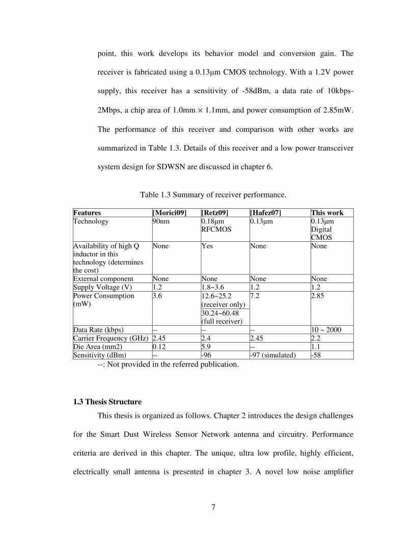
Table 1.3 Summary of receiver performance.
--: Not provided in the referred publication.
1.3 Thesis Structure
This thesis is organized as follows. Chapter 2 introduces the design challenges
for the Smart Dust Wireless Sensor Network antenna and circuitry. Performance
criteria are derived in this chapter. The unique, ultra low profile, highly efficient,
electrically small antenna is presented in chapter 3. A novel low noise amplifier
Features [Morici09] [Retz09] [Hafez07] This work
Technology 90nm 0.18µm RFCMOS
0.13µm 0.13µm Digital CMOS
Availability of high Q inductor in this technology (determines the cost)
None Yes None None
External component None None None None Supply Voltage (V) 1.2 1.8~3.6 1.2 1.2
12.6~25.2 (receiver only)
Power Consumption (mW)
3.6
30.24~60.48 (full receiver)
7.2 2.85
Data Rate (kbps) -- -- -- 10 ~ 2000 Carrier Frequency (GHz) 2.45 2.4 2.45 2.2 Die Area (mm2) 0.12 5.9 -- 1.1 Sensitivity (dBm) -- -96 -97 (simulated) -58

8
design and its optimization guidelines are proposed in chapter 4. The new antenna
and low noise amplifier co-design methodology is introduced in chapter 5. The design
of a low power 2.2GHz on-off keying receiver suitable for SDWSN is discussed in
chapter 6. Chapter 7 concludes this thesis and suggests future work.

9
Chapter 2 Design Philosophy for Smart Dust
Wireless Sensor Networks (SDWSN)
This chapter explores the design philosophy and the state of art of Smart Dust
Wireless Sensor Networks (SDWSN). Low cost, low power, and low volume
requirements are the main hardware design challenges in SDWSN. This chapter
discusses the design trade-offs in detail and proposes a Direct Demodulation Receiver
(DDR) architecture as the low power receiver design most suitable for SDWSN. The
performance requirements for each block are briefly studied in this chapter. The
design details for the blocks are discussed in later chapters in this thesis.
This chapter is organized as follows. Section 2.1 introduces Smart Dust
Wireless Sensor Networks and their requirements. Section 2.2 discusses the design
challenges of SDWSN. Section 2.3 discusses some SDWSN design trade-offs.
Section 2.4 reviews the state of art, and proposes a Direct Demodulation Receiver
(DDR) for SDWSNs. Section 2.5 presents the gain, the design criteria, and provides
budget calculations for this DDR. Section 2.6 summarizes this chapter.

10
2.1 Smart Dust Wireless Sensor Networks (SDWSN)
2.1.1 The Concepts of WSN and SDWSN
A Wireless Sensor Network, or WSN, is a low power multi-hop wireless
communication network composed of energy sources (i.e., batteries), sensors,
antennas, RF transceivers, micro controllers, and user interfaces. Many WSNs follow
the IEEE 802.15.4 standard (proposed in the mid 2000’s) [IEEE standard], which is a
fairly new standard in the IEEE 802.15 group. It features a low data rate, long battery
life, and low complexity communication. Table 2.1 is a summary of the IEEE
standards for wireless personal area networks(WPAN). To achieve optimal
performance for the WSN, multiple tradeoffs have to be made between power
consumption, communication protocols, and wireless communications.
Table 2.1 Wireless personal area network (WPAN) IEEE standards.
802.15.1 (Bluetooth)
802.15.3 (High Rate)
802.15.4 (Low Rate)
Application Bluetooth portable imaging and multimedia
ZigBee
Band 2.4GHz 2.4GHz 868MHz, 915MHz, 2.4GHz
Data Rate 1Mbps 11, 22, 33, 44, 55Mbps. 20, 40, 250kbps
Comm. Range 100m 1~10m 1~10m
Mod/Demod GFSK1 QPSK2, DQPSK3, 16-QAM4, 32-QAM, 64-QAM
BPSK5, PSSS6, O-QPSK7
GFSK1: Gaussian Frequency Shift Keying QPSK2: Quadrature Phase Shift Keying DQPSK3: Differential Quadrature Phase Shift Keying QAM4: Quadrature Amplitude Modulation BPSK5: Binary Phase Shift Keying PSSS6: Parallel Sequence Spread Spectrum Keying O-QPSK7: Offset Quadrature Phase Shift Keying

11
The concept of “Smart Dust” was conceived in 1991 [Cook06]. “Smart Dust”
is a member of the WSN family, with strict requirements on radio size and power
consumption; the system does not need to follow existing communication standards.
Each wireless sensor node, or “mote”, is assumed to have a compact volume in the
range of cubic millimeters to centimeters (the size of grains of “smart dust” at the low
end), which contains one or more sensors, computation units, power supplies, and
communication blocks [Cook06]. When used in large numbers, the “motes” form an
autonomous wireless sensor network: the motes sense the environment and
communicate with each other over short distances (typically around 10m) using
multiple hops. Such intelligent wireless sensor networks can be used in managing
large inventories, monitoring product quality, monitoring environmental conditions
for crop growth, monitoring patients in hospitals, building virtual keyboards, and in
many other application [Warneke01].
2.1.2 Smart Dust Requirements
With devices continuously scaling down in size, low power, low cost, high
device density, high speed digital and radio frequency analog circuits are becoming
available [Abidi04]. In addition, technology advances in MEMS
(Microelectromehanical systems), energy scavenging, and long lasting batteries have
made wireless sensor motes a reality instead of science fiction.
Various research groups have made progress in designing and fabricating
“Smart Dust” hardware over the last decade. Pioneering works include the “Smart
Dust” project led by Dr. Pister and Dr. Kahn at University of California, Berkeley

12
[Kahn99], the “PicoRadio” project led by Dr. Rabaey at University of California,
Berkeley [Rabaey02, 06], and the “WiseNET” project led by Dr. Vittoz at the Swiss
Center for Electronics and Microtechnology Inc (CSEM) [Porret01]. Commonly
accepted SDWSN features realized by these works are (but are not limited to):
• Low power consumption: The average power consumption is 100µW for up to
one year. The on-state power consumption goal is 2mW. Duty cycles are on
the order of 1%.
• Low form factor: around 1cm3 in volume and unobtrusive to the environment.
• Low cost: less than US $1 for each mote.
• Low communication range: 1 to 10m.
• Low data rates: bit rate is on the order of kbps.
• BER (Bit Error Rate): less than 10-4.
• Transmitted power: less than 1mW.
• Packet lengths: between 20 bits for the control packets to 200 bits for typical
data packets, with a maximum packet length of 500 bits.
• Noise Figure: around 20dB.
2.2 Design Challenges
Among the above requirements, achieving low power, low cost, and low form
factor are the major objectives and challenges in the SDWSN transceiver front-end
circuit design. In this section, we explain the importance of these three design
endeavors. In the next section, we discuss the design trade-offs.

13
2.2.1 Low Power
A SDWSN requires that each “mote” in the network function properly from
one to ten years. It is very costly and not advisable to change batteries on each of the
large number of “motes” during their lifetimes. The circuitry power is determined by
the power density and the size of the energy source. Available energy sources
currently include Lithium (non-rechargeable or chargeable), Alkaline, NiMH, Zinc-
Air batteries, solar cells, and energy scavenging devices. For a 1cm3 volume Smart
Dust node, the average power consumption provided by a Lithium battery is around
100µW / cm3 × 1 cm
3 = 100µW, if the battery lifetime is up to 1 year [Rabaey02]. This
extremely low power supply level seriously challenges the SDWSN transceiver
design, because the available power supply is directly related to the signal strength,
noise level, sensitivity, communication distance, carrier frequencies, etc.
2.2.2 Low Cost
Deploying a large number of Smart Dust nodes in WSNs is feasible only if the
cost of each node is trivial. In order to minimize this cost, the unit hardware demands
a very high level of integration. For example, receiver architectures free of bulky
external filters, such as Direct Conversion Receivers (DCR), are preferable to
heterodyne receivers. The latter typically have high quality factor (Q) Surface
Acoustic Wave (SAW) filters that are very difficult to achieve with on-chip devices,
requiring additional fabrication and assembly costs. In addition, RF, analog, and
digital circuits should be consolidated into a single die to increase the level of
integration. The die area should also be minimized to reduce cost.

14
Present market available WSN hardware, such as TelosB [Crossbow]2, have
not quite achieved the 1 US$ cost goal. It is urgent to break this cost barrier to make
affordable hardware for SDWSN applications.
2.2.3 Low Form Factor
As already discussed, to deploy a large scale SDWSN and reduce the cost,
maximal integration and minimum chip area are necessary. In addition to the cost
related to the low form factor requirement, Smart Dust motes used in some scenarios,
such as security surveillance, monitoring, or defense applications, need to be
inconspicuous. A total node volume (including sensor, antenna, battery, circuitry,
etc.) of 1cm3 or less is appropriate. Accordingly, the area of the chip package should
be about 1cm2.
2.3 Design Trade-Offs
The tradeoffs between SDWSN hardware power, cost, form factor constraints,
and performance are shown in Fig. 2.1.
2 TelosB uses TI, CC2420 as its radio.

15
To reduce cost, die area must be minimized. With 0.13µm technology,
capacitors up to a few tens of pF and inductors of between a few hundreds of pH to a
few nH are feasible on a chip. Due to design rule limitations and electromagnetic
(EM) noise coupling, inductors cannot be arranged in a compact fashion. Multiple
inductors must be arranged far enough from other components to minimize harmful
EM coupling. It is essential to limit the total number of inductors and to use only
small value inductors and capacitors. However, with small inductors and capacitors,
transceivers can only work at high frequencies. This negatively affects receiver
sensitivity and power consumption, as explained below.
It is well known that for CMOS transistors, the minimum intrinsic noise factor
Fmin is proportional to the ratio of the operating frequency ω to the unity gain
frequency ωT (2.1) [Lee03].
( )2
min 15
21 cF
T
−+= γδω
ω . (2.1)
Sensitivity
Antenna Size
Form Factor
Battery LifePower
Cost
Communication Distance
Efficiency
Carrier Frequency
Sensitivity
Antenna Size
Form Factor
Battery LifePower
Cost
Communication Distance
Efficiency
Carrier Frequency
Fig. 2.1 SDWSN design tradeoffs.

16
Terms in the square root above are constants that will be explained in detail in chapter
4. The intrinsic noise factor of transistors increases with operating frequency. To
achieve reasonably low noise figures at higher frequencies, ωT=gm/Cgs needs to be
large. gm is the transconductance, which is proportional to power consumption. Cgs is
the gate source parasitic capacitance. Therefore, more power is needed to have same
receiver noise level at higher operating frequencies.
In addition, receivers at higher frequencies radiate and receive less power. We
can define the effective aperture of receiving antenna as Ae≡Gλ2/4π, where G is the
antenna gain and λ is the wavelength [Stutzman98]. Consider two half wavelength
dipole antennas A and B, with λA=0.5λB; the operating frequency of A is twice that of
B. Since the gain of half wavelength dipoles is constant regardless of the operating
frequency:
BeAe AA ,, 41= . (2.2)
If A and B are exposed to the same incident time-average power density Pav, then the
received power levels ArP , and BrP , of antennas A and B, respectively, are
BravBeavAeAr PPAPAP ,,,, 4/141 === . (2.3)
To retrieve the signal over the same communication distance, we can either increase
the receiver sensitivity by 6dB, or quadruple the transmitted power. Either way,
higher power consumption is required.
Considering frequency, power, cost, and performance trade-offs, the bands
used for Smart Dust are 902 to 928MHz in North America, and 2.4 to 2.485GHz
through most of the world (Japan, China, Europe, etc.). Due to noise and interference
in the very crowded 2.4GHz band (Bluetooth and ZigBee are in this band), this work

17
studies and designs SDWSN receivers at 2.2GHz. It is easy to transfer the design to
the 2.4GHz band. Form factors at this frequency may reach the 1cm3 goal with some
effort (chapter 3). This choice of band does not violate Federal Communications
Commission (FCC) regulations at 2.2GHz, because the radiated signal strength is
very low (less than 1 mW), and the communication distance is short (less than 10
meters). In particular, “the FCC has reserved the 2110-2150MHz and 2160-2200MHz
bands for future emerging technologies on a co-primary basis with fixed services”
[NTAIA97].
To successfully design a SDWSN that balances requirements among power
consumption, cost, form factor, sensitivity, communication distance, operating
frequency, antenna size, efficiency, etc., we next review the state of the art and
present a proposed architecture.
2.4 State of the Art
Since the emergence of WSN, many research groups have made substantial
progress in designing SDWSN units over the last decade [Kahn99] [Rabaey02,06]
[Porret01]. This section reviews the state of the art in SDWSN receivers, focusing on
low power, low cost, and low form factor.
2.4.1 Direct Conversion Receiver
Traditionally, heterodyne architecture has been widely used in high-
performance receivers. However, as discussed in section 2.2, highly selective filters
must be used for both the image rejection filter and the intermediate frequency (IF)
filter, which requires bulky external components, such as SAW filters. These high Q

18
filters inevitably increase both form factor and cost, and are not practical for
integration with on-chip CMOS technologies. Direct conversion receiver (DCR)
architectures (also called zero-IF or homodyne) are adopted by designers for WSN
applications, because they are free of bulky high performance filters [Abidi95]
[Razavi97].
Fig. 2.2 shows a block diagram of a DCR, where the RF input is in-
phase/quadrature (I/Q) mixed with its own frequency. The output has zero-
intermediate frequency (IF). The image is the signal itself. Therefore, both the image
rejection filter and the low IF filter are eliminated. All subsequent baseband
processing is performed at very low frequency due to the zero-IF scheme. This is
suitable for low power, low form factor applications. In addition, this architecture can
be applied to any demodulation scheme with I/Q signals. DCRs have been widely
used in WSNs [Darabi00] [Porret01] [Jarvinen05] [Nguyen06].
Fig. 2.2 Block diagram of a direct conversion receiver.

19
However, DCR requires many circuit blocks, such as phase locked loops
(PLLs), oscillators, mixers, etc., which increase power consumption and circuit
complexity. For example, the 915MHz receiver front-end circuit for the ZigBee
standard reported in [Nguyen06] consumes 3.6mW alone, excluding the power
consumption of PLLs and voltage controlled oscillators (VCOs). If this power were
considered, the communication node would be well above the 1-2mW power budget.
In addition to more power consumptions, in order to achieve accurate
frequency control, a DCR often needs an external crystal oscillator, which reduces the
receiver integration level. Furthermore, additional techniques (i.e., digital calibration)
need to be applied to solve well-known DCR problems, such as (1) DC offset, (2)
even-order distortion, (3) flicker noise, (4) I/Q mismatch, and (5) local oscillator (LO)
leakage, which degrade signal the noise ratio (SNR) of the receiver if left untreated.
To solve these problems without adding additional circuits, low IF receivers can be
used.
2.4.2 Low IF Receiver
If we change the down converted signal from zero-IF to a low-IF, the DC
offset problem in the DCR is eliminated. Although a low-IF receiver reintroduces the
image problem, the image rejection requirement is much relaxed. This type of low-IF
receiver is often a choice for low power WSN applications [Kluge06]
[Choi03][Sheng03].
Fig. 2.3 is the block diagram of a low IF receiver. The incoming signal is first
amplified by a LNA, and then down-converted to a low IF signal through I/Q mixers.

20
This low IF signal is then demodulated after channel selection filters and limiting
amplifiers. The choice of IF involves many tradeoffs: If the IF is too low, 1/f noise
becomes important, which reduces the signal to noise ratio. In addition, PLL locking
time is longer if an integer-N frequency synthesizer PLL is used. If the IF is too high,
then the circuit blocks after the mixers, such as channel selection filters, need to be
high Q and consume more power. Low-IF architecture has comparable complexity to
DCR, and consumes about the same amount of power as DCR.
2.4.3 Super-Regenerative Receiver
To further decrease the power consumption level and form factor, simpler
receiver architectures with fewer circuit blocks should be considered. One of these
simple, low power receivers is the super-regenerative receiver, which was invented
by Armstrong in 1922 [Lee03]. The super-regenerative receiver is essentially an
oscillator that is turned off periodically by a “quench” signal to remove the saturation
effect. This very low power and highly efficient super-regenerative receiver was
revisited recently in [Otis05]. An example of a highly integrated super-regenerative
Fig. 2.3 Block diagram of low-IF receiver.

21
OOK receiver for WSN applications is presented in [Otis05], and its block diagram is
in Fig. 2.4.
In the super-regenerative receiver, an isolation amplifier provides matching to
the antenna. It also isolates the oscillator and the antenna to prevent the signal from
being re-transmitted from the oscillator in receiving mode. The detector oscillator
samples the RF input as its initial condition. In OOK demodulation, by periodically
applying the quenching to the oscillator, the oscillator will be activated when seeing
sampling bit-1, and deactivated when reading sampling bit-0. The oscillation
envelope is detected by a nonlinear filter. A pulse width demodulator then removes
the oscillator sampling tone, leaving a raw OOK signal for an OOK detector.
Due to the minimum number of active components and very simple
architecture, this OOK consumes only 400µW, and has a sensitivity of -100.5dBm at
5kbps for BER = 10-3. However, in this circuit, the free running frequency of the
oscillator is set by a bulk acoustic wave (BAW) resonator, which is not common in
standard CMOS technologies, and increases fabrication and assembling costs. For this
Fig. 2.4 Block diagram of super-regenerative receiver [Otis05].

22
reason, we do not consider this architecture in the SDWSN CMOS receiver design in
this work.
Nevertheless, the concept of “going back to fundamental simple receiver
architectures” has motivated us to propose a direct demodulation receiver
architecture, which is described in the next section.
2.4.4 Proposed Receiver Architecture: Direct Demodulation Receiver (DDR)
Since a SDWSN uses low data throughput, we can pick up receiver
architectures and modulation/demodulation schemes that are suitable for low data
rates. WSN IEEE Standards employ BPSK, O-QPSK, GPSK, etc. as
modulation/demodulation methods for low data rate applications (Table 2.1), but do
not specify methods for SDWSNs. In fact, frequency shift keying (FSK), binary
frequency shift keying (BFSK), amplitude shift keying (ASK), and on-off keying
(OOK) may all be good candidates for SDWSN.
ASK is commonly used in broadcast radios and television audio. Due to its
susceptibility to noise and need of a highly linear power amplifier (PA), ASK is not
used in today’s wireless systems. However, a simple ASK modulation/demodulation
method, the on-off keying (OOK) method was used in this SDWSN project, since
there is only one channel in this network. In OOK systems, PA linearity is not
important. We propose a direct demodulation receiver (DDR) for this OOK
modulation/demodulation method. The block diagram of this OOK receiver is shown
in Fig. 2.5. It has only 3 function blocks: input gain stage, demodulation stage, and
output gain stage.

23
For an OOK transceiver, power is cycled to turn on the transmitter when
sending bit-1, and turn it off when sending bit-0. To retrieve the signal, a
straightforward way is to apply an envelope detector or amplitude detector in the
demodulation block. A DDR should amplify the received RF signal to a level that can
be processed by the envelope/amplitude detector. This may require additional
amplifying stages after the LNA. After filtering, shaping, and further amplifying of
the demodulated signal, the digital stream is ready to be processed by baseband
digital circuits.
The proposed receiver architecture is simple and requires very few circuit
components while demanding no external parts except for an antenna. It is therefore
suitable for low power, highly integrated applications, such as SDWSNs.
2.5 Receiver Design Goals
For very small input signals, the receiver needs to meet certain gain and noise
specifications to function properly. This section studies first the receiver sensitivity
requirements. Then, it estimates the gain and noise budget for each block of the
SDWSN DDR.
Fig. 2.5 Block diagram of direct demodulation receiver (DDR) for OOK.

24
2.5.1 Sensitivity Requirements
Receiver sensitivity is the minimum detectable signal over a bandwidth,
which is defined as [Razavi97]:
dBoutdBHzdBmSourcedBmSigMin SNRNFBWPP ||log10|| /, +++= . (2.4)
PMin,Sig is the minimum detectable signal in dBm. PSource|dBm/Hz=-174dBm/Hz is
a constant, which is the source resistance noise power per unit bandwidth. BW is
bandwidth in Hertz. SNRout is is the signal to noise ratio measured at the output of the
receiver. The minimum SNRout is determined by the required Bit Error Rate (BER).
For OOK with BER = 10-4, SNRout = 16dB. NF is the noise figure of the receiver,
which is the ratio of the total equivalent noise power at the input to the noise power of
the source resistance (in dB). Ideally, if the system is noise free, then NF is 0dB. In
reality, NF is often much larger than 0dB. For WSN, the achievable NF is around
20dB according to [Porret01]. Eqn. (2.4) tells us that over a unity bandwidth, the
minimum detectable signal of the receiver must be higher than the thermal noise level
of the system by at least the sum dBoutdB SNRNF || + . For receivers with larger noise
factors and requiring higher SNRout, SigMinP , is larger. Weaker incoming signals cannot
be detected.
The power available at the input of a receiver in free space is defined in (2.5)
[Kraus88]:
( )2
2
4 d
GGPP rt
trπ
λ= . (2.5)
In (2.5) Gr and Gt are the receiving and transmitting antenna gains. Pr and Pt are
received and transmitted power. λ is the wavelength of the transmitter and the

25
receiver. d is the distance between them. As it will be seen in chapter 3, low profile
antennas designed for this work have a gain of -1.38dBi. The wavelength at 2.2GHz
is 0.1364m.
For non-ideal communication environments, such as an indoor environment,
an additional attenuation factor is introduced to (2.5) [Rappaport96]. Eqn (2.5)
becomes
( )
n
rttr
d
d
d
GGPP
= 0
2
0
2
4π
λ . (2.6)
d0 is called the close-in distance. It lies in the antenna far-field region and is much
smaller than the desired communication distance d. For “Smart Dust” applications, d0
= 1m. n is the path loss modification index that represents the attenuation beyond d0,
and is commonly chosen to be 4 or less for low GHz frequency. In (2.6), the factors
that define signal attenuation are called path loss PL, which are re-written in (2.7).
( )( )
2
0
2
0
4n
t t r
r
dPG G dPL d
P d
π
λ
= = ⋅
(2.7)
Table 2.2 lists path losses for 2.2GHz SDWSN vs. communication distance and the
path loss modification index.
Table 2.2 Path loss (dB) for 2.2GHz SDWSN communication.
d = 2 d = 3 d = 4 d = 5 d = 6 d = 7 d = 8 d = 9 d = 10
n = 2 45.3 48.83 51.33 52.27 54.84 56.19 57.35 58.37 59.29
n = 3 48.3 53.6 57.35 60.26 62.63 64.64 66.38 67.92 69.29
n = 4 51.3 58.4 63.4 67.25 70.41 73.09 75.41 77.46 79.3
d (m): communication distance n: path loss modification index

26
The minimum signal available to the receiver is determined by (2.6). We assume this
level is also the receiver sensitivity level. If the transmitter’s efficiency is 40%, the
dependence of receiver sensitivity on communication distance and modification index
can be plotted in Fig. 2.6.
From Fig. 2.6, we can estimate another important receiver characteristic,
which is the dynamic range. The receiver’s dynamic range is defined as the difference
between the maximum and minimum detectable signal. From Fig. 2.6, receiver
dynamic range is around 34dBm (Psense,max – Psense,min = 34dBm). This means, the
receiver should be able to detect signals as weak as -80dBm at 10 meters under
maximal levels of path loss, and should process signals as strong as -46dBm when
communicating over short distances in a near free space environment (n=1).
Due to the absence of a high quality factor filter in front of the LNA, the
bandwidth of the LNA is much wider than the baseband signal bandwidth. This
Fig. 2.6 Sensitivity of receiver vs. communication distance d and modification index n.
Left: transmitter dissipates 1mW. With 40% efficiency, effectively transmitted
power=0.4mW. Right: transmitter dissipates 2mW. With 40% efficiency,
effectively transmitted power=0.8mW.
(a) (b)

27
means that the noise bandwidth is much larger than the signal bandwidth. The
receiver sensitivity should be estimated with the larger noise bandwidth. For example,
according to (2.4), if the LNA has a bandwidth of 20MHz at 2.2GHz, and then for a
mid range sensitivity of (-80 - 46.56) / 2 = -63.3dBm and a signal to noise ratio of
16dB, the NF of the system is 21.7dB. The minimum NF of the receiver needs to be
5dB if sensitivity of -80dBm is required. We next determine the required noise figure
for LNA.
2.5.2 Receiver Budget
The OOK receiver block diagram was shown previously in Fig. 2.5. To bring
the signal to a detectable level in the demodulator block, a second gain stage is added
after the LNA; the receiver chain is re-plotted in Fig. 2.7.
According to Friis equation [Friis44], for m cascade stages, the total noise
factor is
Fig. 2.7 OOK receiver block diagram with gain and noise estimations.

28
pmpp
m
ppp
totGGG
F
GG
F
G
FFF
...
1...
11
2121
3
1
21
−++
−+
−+= . (2.8)
Fi is the noise factor and Gi is the gain of the ith stage, respectively. According
to (2.8), if receiver has NF = 5dB (receiver sensitivity is -80dBm), then 5dB = 1.38dB
+ NFb, where NFb = 3.63dB is the noise figure of the receiver circuit excluding the
antenna. The noise figure from point b to f of the above receiver chain is calculated
as:
−+
−+
−+=
−
+−
+−
+=
−122
5.1
22
5.1
2
5.1
1010
101010
10
1010
10
10
1010
10
101010
110
1010
110
10
11010log10
101010
110
1010
110
10
11010log10
432
5
32
4
2
3
LNA
vvpvpp
LNA
NF
GGG
NF
GG
NF
G
NFNF
bNF
. (2.9)
It can be seen that if NFLNA = 0dB (the ideal case, a noiseless LNA), then NFb
is 1.27dB. If NFLNA = 3dB, the noise figure seen from b to f is 3.69dB. Therefore, the
LNA should have a noise figure around 3dB in this design to meet the best sensitivity
requirements.
2.6 Conclusion
This chapter introduces the concept and requirements of Smart Dust Wireless
Sensor Networks (SDWSN), and then studies the relevant design challenges. After
reviewing the state of the art of Wireless Sensor Network receiver design, a Direct
Demodulation Receiver applying on-off keying is proposed. This architecture is low
power, has low form factor, and eliminates off-chip components except for a low
profile, highly efficient antenna. It is suitable for SDWSN. Design details of each
block of the receiver and the compact antenna are discussed in the following chapters.

29
Chapter 3 Scalable Highly Efficient
Electrically Small Antennas (ESA)
As described in chapter 2, a complete Smart Dust Wireless Sensor Network
(SDWSN) node should have a total volume of less than one cubic centimeter,
including the transceiver integrated circuit (IC), battery, sensor, antenna, and ground
plane. The millimeter or centimeter scale dimensions are often a small fraction of a
quarter wavelength at the operating frequency, which makes efficient electrically
small antenna (ESA) design very challenging. This work introduces a novel low
profile 916MHz F-Inverted Compact Antenna (FICA) with a volume of 0.024λ ×
0.06λ × 0.076λ, ground plane included. The radiation efficiency is 48.53% and the
peak gain is -1.38dBi. The designed antenna can be scaled to higher operating
frequencies, such as the 2000 to 2500 MHz bands with comparable performance,
whereas the volume is significantly reduced. Ground plane effects and a circuit model
are also discussed in this work.
This chapter is organized as follows. Section 3.1 reviews existing work in
ESAs. However, ESA suitable for SDWSN is a very new research area for which
little work has been done. For this reason, section 3.2 summarizes the unique
characteristics and particular requirements for ESAs in SDWSN. According to these

30
design demands, section 3.3 proposes design guidelines for ESAs. Following these
guidelines, a novel ESA (F-inverted compact antenna (FICA)) is proposed in section
3.4. Specifically, design considerations, FICA structure, operation principles,
simulation, measurement results, and parametric sensitivity are discussed in this
section. It is well known that the ground plane size is one of the dominant factors in
ESAs’ performance and overall size. The ground plane effect of FICA is studied in
section 3.5. In section 3.6, we develop a measurement-based, simple, useful, and
accurate FICA circuit model readily usable in circuit simulators of system design.
Another advantage of the proposed antenna is its ability to be scaled to other
frequencies. This is demonstrated in section 3.7. Finally, section 3.8 concludes by
discussing the novelty and advantages of this work.
3.1 ESA State of the Art
Electrically small antennas (ESAs) have been a topic of interest for more than
half-century [Wheeler47] [Chu48]. The proliferation of personal wireless
communication devices, such as cell phones and PDAs (Personal Digital Assistant),
has greatly stimulated the design of ESAs [Morishita02]. This section explores
different types of ESAs built for mobile hand held devices. These antennas embody a
large amount of progress and innovation in miniaturization.
Printed Dipoles
As will be explained in section 3.2, antennas with near omnidirectional
radiation pattern are suitable for SDWSNs. Dipole antennas have omnidirectional
radiation patterns in the plane normal to their axis. To reduce the form factor, dipole
31
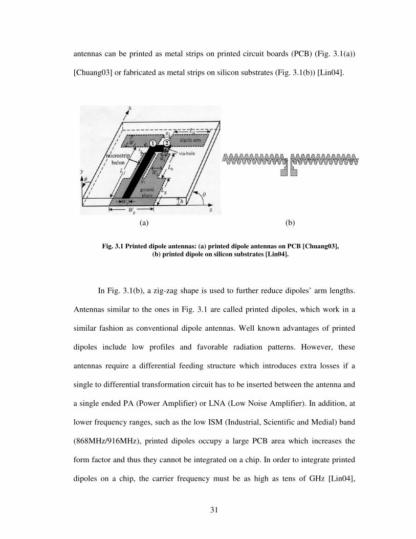
antennas can be printed as metal strips on printed circuit boards (PCB) (Fig. 3.1(a))
[Chuang03] or fabricated as metal strips on silicon substrates (Fig. 3.1(b)) [Lin04].
In Fig. 3.1(b), a zig-zag shape is used to further reduce dipoles’ arm lengths.
Antennas similar to the ones in Fig. 3.1 are called printed dipoles, which work in a
similar fashion as conventional dipole antennas. Well known advantages of printed
dipoles include low profiles and favorable radiation patterns. However, these
antennas require a differential feeding structure which introduces extra losses if a
single to differential transformation circuit has to be inserted between the antenna and
a single ended PA (Power Amplifier) or LNA (Low Noise Amplifier). In addition, at
lower frequency ranges, such as the low ISM (Industrial, Scientific and Medial) band
(868MHz/916MHz), printed dipoles occupy a large PCB area which increases the
form factor and thus they cannot be integrated on a chip. In order to integrate printed
dipoles on a chip, the carrier frequency must be as high as tens of GHz [Lin04],
Fig. 3.1 Printed dipole antennas: (a) printed dipole antennas on PCB [Chuang03],
(b) printed dipole on silicon substrates [Lin04].
(a) (b)

32
which impacts the communication range as we discussed in chapter 2. Therefore, for
lower GHz frequencies, we need to find other antennas to simultaneously satisfy the
communication range and form factor limit.
Dielectric Resonance Antennas
If a dielectric resonator is not placed inside a metal enclosure, it can act as a
radiating dipole. This property has been used to build dielectric resonance antennas
(Fig. 3.2 [Mongia97]), which have compact size and the flexibility to operate at
different frequencies using different modes. However, their radiation efficiency is
medium, and the cost for mass production is high, which is not suitable for SDWSN
[Mongia94, 97].
Microstrip Patch Antennas
Microstrip patch antennas are cost effective and easily integrated with Radio
Frequency Integrated Circuits (RFIC) or Millimeter wave Integrate Circuits (MMIC),
Fig. 3.2 Rectangular dielectric resonance antenna placed on a ground plane [Mongia97].

33
so they are very popular in portable wireless communication devices. Fig. 3.3 is a
diagram of a patch antenna. In Fig. 3.3, a metal rectangular patch printed on a printed
circuit board (PCB) is separated from its parallel ground plane by a small distance.
This structure forms a simple open cavity radiator, which emits energy from its edges.
Radiation propagation is in the direction perpendicular to the patch. The patch
antenna in Fig. 3.3 can be excited by a microstrip feed line over the ground plane.
Because of their low profiles, patch antennas have very narrow bandwidth [Wong03].
Like printed dipoles, they need to be about one half wavelength long in the dielectric
at 900 MHz or lower GHz range [Wang05]. Therefore, conventional patch antennas
are not usable in low GHz SDWSN.
Monopole Antennas, Inverted-F Antennas (IFA)
Monopole antennas and their variants, such as inverted-F antennas (IFA) (Fig.
3.4), are often seen in cell phones, Bluetooth, and other small wireless devices.
Fig. 3.3 Microstrip patch antennas.

34
These antennas use the device ground plane as the other half of the antenna
and have a radiation pattern close to omnidirectional. IFA is essentially a variation of
the transmission line antenna. The current flows from the feed to the horizontal arm
where it meets the current flowing from the shorted stub to the horizontal arm.
Currents in the microstrip feed and shorted stub are closely coupled and are in the
same direction which contribute radiation. The current in the horizontal arm returns to
the ground plane through free space displacement current. Depending on coupling
strength, this portion of the current may or may not help boost radiation.
IFAs have impedance matching flexibility, and the best matching is normally
determined experimentally. However, if the ground plane size is less than a quarter
wavelength, impedance matching becomes very hard [Zhang05, Soras02]. For 900
MHz or lower GHz SDWSN applications, the ground planes must be much smaller
than a quarter wavelength for an inconspicuous “mote”, which makes standard IFAs
impractical.
Fig. 3.4 Diagram of an inverted-F antenna (IFA).
PC board
Microstrip
Feed
Shorted to
ground
plane Metal ground
plane at the
backside of PCB
Backside of PCB is
free of metal
Metal

35
Planar Inverted-F Antennas (PIFA)
Planar Inverted-F Antennas (PIFA) [Boyle06] (Fig.3.5), as a combination of
the patch antenna and IFA [reference], have a wider bandwidth than IFA due to the
radiating patch. Depending on the distance from the patch to the ground plane, it may
have moderate to high gain in both vertical and horizontal polarization. However, the
performance of PIFAs greatly depends on the ground plane size [Huynh03, Chen05].
To reduce the size of a PIFA and design dual band or multi band antennas, meander
lining [Pham04] has been introduced to reduce the length of microstrip antennas,
IFAs, or PIFAs [Wong02]. However, the RF currents in the immediate adjacent
conductors flow in opposite directions, which reduces the efficiency of the antenna.
In addition, the ground plane limit still exists regardless of the meander line.
Fig. 3.5 Planar Inverted-F antennas (PIFA) (left) [Boyle06] and
meander line PIFA (right) [Pham04].

36
Antenna optimization Using Genetic Algorithms (GA)
In addition to traditional antenna designs, genetic algorithms (GA) can be
applied to optimize wire antennas [Choo05] (Fig. 3.6), but this requires an infinite
ground plane for optimization. Usually the optimized results have sharp turning
angles, which cause current crowding problems. In addition, it is difficult to duplicate
the geometries of wire antennas according to the three-dimensional (3D) optimization
calculation results.
Electromagnetic Band-Gap (EBG) Structures
Using electromagnetic band-gap (EBG) structures (Fig. 3.7) [Bell04] as
ground planes, or mimicking the presence of a perfect magnetic boundary (PMC)
[Abedin03], are techniques that have been explored to enhance the performance of
antennas with reduced height. Again, in the above antenna miniaturization
technologies, a minimum quarter wave length ground plane is required, whose
dimensions tend to overwhelm the size of the antenna. Therefore, these solutions may
Fig. 3.6 Genetic algorithm antennas [Choo05].
Left: theoretical design. Right: photo of implemented antenna.

37
not be appropriate candidates for SDWSN.
3.2 The Need for ESA in Smart Dust System
While many ESAs for conventional handheld devices have demanding
requirements, such as low cost, low weight, compact profile, gain, and bandwidth
performance, antennas in ultra low volume Wireless Sensor Network (WSN)
applications have even stricter dimensional limitations and demand radiation to be as
omnidirectional as possible for the following two reasons:
First, in each WSN transceiver node, all components, such as the sensor,
antenna, battery, transceiver integrated circuit (IC), as well as the reference ground
plane (normally a printed circuit board) for the IC, and the antenna are stacked or
integrated in a package with a total volume of only a few mm3 to one cm3
[Rabaey02], and only a fraction of this volume is left for the antenna. The millimeter
or centimeter scale dimensions are often much less than a quarter wavelength at the
Fig. 3.7 A spiral antenna with electromagnetic band-gap (EBG) structures [Bell04].

38
operating frequency (i.e., 0.1λ or less). For example, it is not unusual to find ISM
band antennas with very small physical size in the literature, as well as in the market
[Mitsubishi]. As discussed in section 3.1, nearly all designs demand a ground plane
with a minimum quarter wavelength dimension for proper performance. As an
example, in the ISM bands (916/828/433MHz), this ground plane size is between 8cm
to 16cm. Though it is a reasonable size for a cell phone or a PDA, it is too large to be
integrated into a SDWSN communication package. Therefore, a conventional
handheld device package with low height and large ground plane area is not suitable
for WSN applications. From a design point of view, the effect of a truncated ground
plane has to be considered in the process of antenna miniaturization. In WSN, the
ground plane size must be decreased just as the height of the antenna. This requires
new designs to reduce both factors and keep the antenna highly functional.
Second, in SDWSN applications, a large number of transceiver nodes are
distributed randomly. These transceiver nodes, as well as the antennas associated with
them are therefore scattered in various directions and form an autonomous
communication network. Each communication node in this network is a complete self
powered transceiver node, which requires the antenna to have a radiation pattern as
omnidirectional as possible to transmit and receive signals in and from all directions
due to the random orientation of the nodes.
To demonstrate a SDWSN with a few “motes”, we need to integrate an
appropriate antenna to a market available WSN radio, as well as sensors and batteries.
At the time of this work, CC1110 at ISM band (916MHz) is used as the radio. At this
frequency, the antenna must achieve the following design goals:

39
1. The antenna must occupy a volume as small as possible. Since the circuit
board must be at least 20mm × 25mm to fit in the commercial radio, sensor,
battery, and other supporting elements, we limit the volume occupied by the
916MHz antenna to be 20mm × 25mm × 8mm (which is 0.06λ × 0.076λ ×
0.024λ).
2. The antenna must have as omnidirectional a radiation pattern as possible in
order to transmit to and detect signals from random directions.
3. The antenna must be optimized for maximum efficiency and bandwidth, since
small antennas inherently have high quality factor (Q) or low efficiency.
3.3 Design Guidelines for ESAs
It is well-known that ESAs have fundamental limitations [Wheeler47; Chu48;
Hansen81; McLean96], such as efficiency, bandwidth, radiation resistance, etc. In
this section, we analyze trade-offs between antenna size and performance that must
be considered in ESA designs, and propose some general design guidelines for ESAs.
3.3.1 Antenna Height
In general, ESAs are understood as antennas that can be enclosed in a sphere
of radius less than a quarter wavelength of the operating frequency. By nature, these
antennas have low driving point resistance. For example, the impedance of a short
dipole type antenna is [Hansen81]
)tan(
)1/(ln)(20 02
kh
ahZjkhZ
π
−−≈
, (3.1)
where k=2π/λ is the wavenumber, λ is the wavelength, h is the dipole half-length, a is

40
its radius, and Z0 is the intrinsic impedance of the medium (120πΩ in free space). The
radiation resistance drops as the square of the height of the antenna according to (3.1),
so that e.g., the typical radiation resistance of an antenna with a height of λ/20 above
a ground plane is only a fraction of an Ohm. Designing a proper matching network to
transfer power into and from a standard 50Ω port becomes extremely challenging.
Given this limitation, the first design guideline is to maximize the possible height of
the antenna in order to achieve maximum efficiency in ESAs.
3.3.2 Antenna Loss
The small size of an antenna not only limits the radiation resistance, but also
causes a driving point reactance which is difficult to match. Again, for maximum
power delivery to ESAs, their reactive component (e.g., the capacitive input
reactance, the imaginary part in (3.1)) needs to be tuned out so that the feed point
impedance is conjugately matched to the standard 50Ω of most test equipment, and to
bring the resonance frequency to the design value.
Using a tuning reactance is a common way to achieve this goal. Using lumped
inductors, air cored wire inductors, or dielectric material loaded inductors will
provide the necessary tuning reactance for a small dipole. In spite of the volume that
these components may occupy a limited space, the dielectric loading material or
inductors may also introduce RF losses and severely reduce the efficiency of the ESA
for the following reasons: (1) Small antennas are effective only if they can carry
relatively large currents with consequently possibly high ohmic losses. The ohmic
resistance due to the skin effect at the operating frequency (916MHz) cannot be

41
neglected, considering the low radiation resistance of small antennas. This ohmic loss
reduces the gain and efficiency of these antennas. (2) It is known that most dielectric
materials are much more dissipative than air. In addition, a dielectric material tends to
store electric energy and reduce radiation. The above two characteristics of dielectric
materials will severely limit the efficiency of the antenna.
Therefore, minimizing losses in radiating components, matching networks and
tuning parts are mandatory guidelines in ESA design. Small cross section conductors,
such as metal strips, are poor materials for small antennas. Where possible, wires are
preferable to strip lines for small antenna applications. In addition, dielectric loading
will also affect the usable bandwidth, as explained in the next section.
3.3.3 Antenna Volume
Due to the small radiation resistance and the associated reactive components,
ESAs are notorious for their gain and bandwidth limitations. Wheeler [Wheeler47]
first explained that the size relative to the operational wavelength limits the
efficiency-bandwidth product of a small antenna. Chu [Chu48] derived the lower
bound of the quality factors (Q) of ESAs
kaakQ
1133
+= , (3.2)
with k the wave number, and a the radius of the sphere enclosing the ESA. These
works are summarized by Hansen [Hansen81]. McLean improved this lower bound in
1996 [McLean96]. It was found that in reality, the quality factor is always higher than
these predictions in lossless cases. Thiele [Thiele03] has recently proposed a new
lower bound of the quality factor for ESAs based on the far-field pattern for dipole

42
type antennas. This lower bound is higher, and it is closer to the value that can be
approached in practice. Nevertheless, (3.2) still gives us a good indication about the
range for Q that is expected in small lossless antennas. This Q is inversely related to
the bandwidth (BW) for ESAs.
As we have mentioned in the last section, while loading antennas with
dielectric materials reduces the dimensions of antennas, it also reduces the antenna
usable bandwidth for the reason in (3.2). Therefore, we should be very careful when
applying dielectric loading to the antenna due to these considerations of both
efficiency and bandwidth.
It is worth emphasizing the role of a in (3.2) when estimating the bandwidth
of ESAs. Recall that a in (3.2) is the radius of the sphere enclosing the ESA. It is not
uncommon to find very low volume chip antennas on the market, which require a
quarter wavelength ground plane to operate properly. The size of that ground plane
limits the minimum a in (3.2) (i.e., / 8a λ= ), which results in a very reasonable
bandwidth. If the ground plane size is much less than a quarter wavelength, it can be
seen clearly that Q increases and the BW drops.
For the above reasons, we should balance tradeoffs when reducing the antenna
size. Fully using all of the allowed volume is an important design guideline in ESAs
to achieve enough bandwidth.
3.4 Innovative ESAs: F-Inverted Compact Antennas (FICAs)
This section proposes a novel low volume F-inverted compact antenna (FICA)
[Yang07a,09a] in the ISM band (916MHz), which follows the guidelines in section
3.3, and meets the design goals in section 3.2. Care has been taken when measuring

43
the gain and radiation pattern of the FICA (the reason is explained in section 3.4.4). A
simple, physics-based circuit model has been devised, which helps in antenna-circuit
interface designs. The antenna is essentially a short monopole (0.024λ) over a ground
plane with a helical impedance matching transmission line. This FICA has a radiation
efficiency of 48.5%, and can be scaled to higher or lower frequency bands.
3.4.1 Design Origins
Folded Dipole
This section reviews the theory of folded dipoles which inspired the design of
FICA. The principle of operation for folded dipoles is similar to the proposed FICA.
A diagram of a folded dipole is plotted in Fig. 3.8. A folded dipole is formed
by folding the arms of a balanced dipole antenna and shorting the end of these two
arms together. Since the parallel lines in a folded dipole are separated by a very short
Fig. 3.8 Operation principles of folded dipole antennas.

44
distance, there is strong mutual coupling between these two arms. Therefore, the
current and voltage of a folded dipole can be decomposed into the antenna mode and
transmission line mode components (Fig. 3.8).
In the antenna mode, the currents in the two arms are in the same direction
and are excited by two sources of voltage V. Any current asymmetry between two
arms can be evaluated by introducing a current sharing factor a . According to Fig.
3.8, the input impedance seen from excitation is:
( ) a
aIa
VZ
+=
1 . (3.3)
In transmission line mode, currents in the arms form a loop. The currents tI in
each arm have the same amplitude but opposite phase. According to Kirchhoff’s
Voltage Law (KVL), the sum of voltage in the antenna’s right arm in antenna mode
and transmission line mode (Fig. 3.8) equals the voltage in the right arm for a dipole
antenna, which is zero. Similar to transformers, the voltage on the left arm is
multiplied by a factor of a if the current in the right arm is multiplied by a factor of
1/a. The input impedance for transmission line mode is:
)tan()1(
00 xkjZI
VaZ
t
t =+
= . (3.4)
Here, tZ is the impedance of a shorted transmission line, where 0Z is the
characteristic impedance of the transmission line; 0k is the wavenumber in free
space; x is the length from the excitation point to the shorting end of the transmission
line. Therefore, the total input impedance of the folded dipole is

45
( )( )
( )( ) ta
ta
ta
tain
in
ZZa
ZZaZ
Z
Va
Za
V
Va
II
Va
I
VZ
++
+=
++
+
+=
+
+==
2
2
1
1
1
1
)1()1(
. (3.5)
Since a complete communication node is always integrated on printed circuit
board (PCB) with other supporting structures, we could use the PCB as the ground
plane to provide image currents and help the radiation. Bearing these considerations,
several novel ESAs are proposed and analyzed in this work.
3.4.2 Innovative ESAs
This section first describes the design of three novel ESAs for SDWSN, which
follow the general ESA design guide in section 3.3 very well. Then, the operating
principles, simulation, measurement results, and parametric analysis of the most
promising ESA are discussed.
3.4.2.1 Inverted-F Meander Line Wire Antenna (IFMLWA)
We first considered a wire meander line antenna with no dielectric loading
(Fig. 3.9). Our meander line antenna is made with 1mm diameter copper wire. The
ground plane is a FR4 board with the dimensions of 25mm by 40mm, equivalent to
0.08λ by 0.12λ at 916MHz. One end of the wire is perpendicular to and shorted to the
ground plane. The height of the shorting pin is 8mm (0.024λ). The other end of the
wire is open. The antenna has been resonated with a total wire length of about 0.75λ.
The antenna is fed by a SMA (sub-miniature, type A) connector through a hole on the
PCB ground plane. Fig. 3.9 shows the measured S11 of the meander line antenna. The

46
antenna resonates at 916MHz. The -10dB S11 bandwidth is about 40MHz, or about
4.4% of its center frequency.
The total volume of this antenna ( 341023.2 λ−× ) is an order of magnitude
lower than minimum ESAs in the literature with comparable or better bandwidth
(Table 3.1). However, even with this very promising novel meander line antenna, the
ground plane is still too large to meet volume limit in section 3.2. Therefore, we have
modified this initial design by using a dielectric block to shorten the antenna as
discussed in the next section.
3.4.2.2 FICA with Teflon Block and Rectangular Loops
To further reduce the size and maintain good gain and bandwidth
performance, a low loss, low dielectric constant (εr = 2.2) Teflon block is inserted
Fig. 3.9 Measured S11 of the wired meander line with no dielectric loading. The antenna is made with 1mm diameter copper wires. The antenna height is 8mm (0.024λ). The ground plane is 25mm ×××× 40mm (0.076λ ×××× 0.122λ at 916MHz). The
bandwidth is 40MHz, about 4.4% at 916MHz.

47
between the F-inverted meander line wire antenna and the ground plane to shorten the
length of the serpentine. Since the meander line portion of the antenna mainly
provides inductance for impedance matching instead of radiating, the wire can be
wound into loops to obtain the necessary inductance in a smaller volume. Therefore,
we further modify the existing ESA by winding a 0.8mm diameter copper wire and
embedding it into the 10mm × 10mm × 6mm Teflon block. This device was then
termed as a F-inverted compact antenna (FICA). A picture of the prototype FICA is
given in Fig. 3.10, where the shorting and feeding pins are also shown. Both pins are
7mm in height. The end of the copper wire is left open. This antenna is also fed by a
SMA connector through a hole on the FR4 ground plane.
The tapping point of the feeding pin is carefully selected so that the minimum
power reflection occurs at 916MHz, the center frequency of operation. Fig. 3.11
shows the measured S11 of the FICA. As one can see, the antenna resonates at
916MHz. The 10dB bandwidth is 15MHz, about 1.6% of its center frequency. The
Fig. 3.10 Top view (a) and side view (b) of the dielectric loaded FICA antenna. The size of the
ground plane is 20mm ×××× 25mm (0.06λ ×××× 0.08λ at 916MHz). The height of the antenna is 7mm.
The dielectric load is a Teflon block with size 10mm ×××× 10mm ×××× 6mm, and a relative dielectric
constant of 2.2.
(a) (b)
7mm

48
total volume of this antenna is 25mm by 20mm by 7mm (0.06λ by 0.08λ by 0.021λ),
excluding the SMA connector on the back side of the board which is there for
measurement purposes only. In a real integrated sensor network node, this SMA
connector is replaced by the transceiver integrated circuits[Yang07b].
Comparing the meander line antenna and the FICA, we find that we have
achieved a volume shrinking factor of almost 6, a very important accomplishment in
view of the specific application.
However, the above FICA has sharp angles along the wire. Current tends to be
crowded over these bending corners and causes ohmic losses. In addition, by using air
to replace Teflon as much as possible while maintaining the same inductance for
antenna tuning, the already low loss due to Teflon could be further reduced with a
consequent decrease of bandwidth and improved radiation efficiency.
Fig. 3.11 Measured S11 of the wired FICA with Teflon dielectric loading. The geometry
of the FICA is shown in detail in Fig. 3.10. The bandwidth is 15MHz at
-10dB, which is around 1.6% at 916MHz.

49
3.4.2.3 FICA with Lexan and Circular Windings
Due to the reasons given at the end of the last section, we modified this design
by replacing the Teflon block with a thin slice of Lexan material, and adopting coils
with circular or elliptical shape instead of rectangular cross-sections. A photo of a
fabricated 916MHz FICA is shown in Fig. 3.12. The ground plane is a FR4 printed
circuit board (PCB) with a size of 20mm × 25mm. A 0.8mm diameter copper wire
was wound as a helix into a 15mm × 2.5mm × 5mm Lexan® block with relative
permittivity of 2.96 and loss tangent < 0.001.
The Lexan® block provides mechanical support to the wire antenna, which
helps to reduce the effect of vibrations. To minimize the length of the helix, the
dielectric block size is selected without increasing the intercoil capacitance
significantly. The coils are maximally spaced without loss of inductance. This helical
shape enables the antenna to resonate at the desired frequency with much shorter
length than a straight wire, a meander line, or other helices with similar geometry.
The antenna height and volume are selected to maximize the radiation efficiency.
With the helical axis parallel to the ground plane, the height of the antenna is 8mm
above the ground plane, which satisfies the volume design restrictions. One end of the
helical copper wire is shorted to the ground plane (the PCB); the other end is free.
According to HFSS (High Frequency Structural Simulator [HFSS]) parametric
simulations, the spacing of each helical loop is chosen to be 2.5mm, while the
distance from the helix to the ground plane is chosen to be 3mm. The distance
between the ground short and the feeding pin is tuned to achieve a good match at the
operating frequency. The antenna under test (AUT) is fed by a metal feeding pin

50
soldered to a SMA connector through a hole in the PCB. When used in WSN
transceiver nodes, the antenna is fed through a wire that carries signals into and from
the transceiver IC that is attached on the back of the PCB[Yang07b].
3.4.3 Principle of Operation
It is very important to realize that this FICA is different from omnidirectional
mode helix antennas, whose turns support a net current in the axial direction
producing a dipole-type radiation pattern. An efficient helical antenna could not be
used in our application because its height above the ground plane would have
exceeded the relevant specifications in section 3.2. The helix with its axis parallel to
the ground plane is used to tune the capacitance of a very short radiator. In this new
structure, the helix acts as a resonant transmission line matching the reactance of a
short monopole (0.024λ), not as an antenna. The radiation from the helix is nearly
suppressed by the proximal ground. The antenna radiating currents flow in the two
vertical wires, as in inverted F antennas (IFAs); they cause the azimuth
(a) (b)
Fig. 3.12 Photographs of (a) side view and (b) top view of the 916MHz FICA. The total
volume (including ground plane) is 8mm ×××× 20mm ×××× 25mm (0.06λ ×××× 0.076λ ×××× 0.024λ).

51
omnidirectional radiation pattern and the polarization of the antenna. The current on
the helix only gives a negligible contribution to the radiation of the FICA, which is
further verified through polarization measurements as shown in section 3.4.5.
Surface current densities on the metal wires of a FICA in a HFSS [HFSS]
simulation are presented here. HFSS uses Finite Element Method (FEM). The FICA
and its mesh used in this simulation are shown in Fig. 3.13. Fig. 3.14 shows the
current density along the metal wires of the FICA.
Fig. 3.13 Mesh plot of FICA in HFSS simulation.
Zoom
in
Feed pin
Short pin
Cu Helix
Lexan block
PCB (ground plane) Cu screw
(assembling part)
Tapping
point

52
As can be seen clearly in Fig. 3.14, currents in the feeding and shorting pins
are in the same direction, with different densities. Both pins are effective radiating
components for the antenna [Boyle06][Yang07a,09a]. As explained in section 3.3, the
whole antenna, as well as the PCB ground plane and the surrounding environment all
affect the radiation characteristics of the antenna. Therefore, special care should be
taken in measuring the performance of ESAs, as discussed in the next section.
This design not only offers a height reduction compared to a helical antenna, it
has the additional advantage that the relatively strong magnetic field is confined
inside the coils and is unlikely to penetrate into the RF circuits which are integrated
on the other side of the small ground. This makes the RF circuits less vulnerable to
electromagnetic interference from the antenna.
The parameters for mass production of the antenna are completely defined
[Yang09b]: the wire diameter, coil spacing, major and minor radius of the coils,
Fig. 3.14 Current density distribution on FICA wires.

53
number of turns, vertical pin height, bending position, and bending angle. All of the
above parameters have been analyzed through HFSS simulations to optimize the
FICA performance, as discussed in section 3.4.7.
3.4.4 Using Baluns in ESA Tests
It is important to measure the antenna performance without any extraneous
radiating metal parts. Since the ground plane size of FICA is small with respect to the
wavelength of operation, we must pay special attention to the antenna feed line.
Without choking, a current would inevitably be coupled onto the outer conductor of
the feeding coaxial cable due to the small size of the ground plane. This current
becomes part of the radiation process and contaminates gain and radiation
measurements. Quarter wavelength sleeve baluns and ferrite bead chokes are
commonly used to balance feed antennas and reduce feeding cable radiation
[Balzano81][Massey03][Icheln04]. Two or more quarter-wave baluns in a row need
be used to suppress the unwanted RF fields and currents coupled onto the feed cable.
Therefore, we have fabricated an RF choke with 3 baluns to be inserted between the
feeding cable and the antenna under test (AUT) (Fig. 3.15, Fig. 3.16). The RF choke
is made of three pieces of cylindrical copper pipe, each a quarter wavelength long.
The ends of these copper pipes away from the AUT are shorted to the outer conductor
of the feeding cable; the other ends facing the AUT are open.
To evaluate the levels of the current coupled from the antenna to the cable, we
employed an electric field probe (E-probe) to measure the coupling (Fig. 3.15). An E-
probe measures the square of the magnitude of the total near electric field around the

54
antenna [Bassen83]. The E-field probe, fed by a highly resistive balanced
transmission line, is RF transparent and does not disturb the fields under test.
We have compared the near field of a FICA fed by a simple bare coaxial
cable, and that of FICA fed by a cable with RF chokes (Fig. 3.15). The distances
between the tip of the E-probe to the axial line of the coaxial cable is fixed at 20mm
in both measurements. This is the distance of the ground plane at the antenna’s open
end to the axis of the cable. We moved the probe along the cable, starting from the
end of the ground plane, and recorded the electric field magnitude measured every
1.27cm. The test results are shown in Fig. 3.16.
Fig. 3.15 Near field measurement construction.

55
For an antenna fed by a cable with RF chokes (Fig. 3.16 (a)), a much larger E-
field reading was recorded between the end of the ground plane and the cable right
under the antenna. A lower E-field value was recorded between the antenna and the
simple bare coaxial cable (Fig. 3.16 (b)). These results indicate that more current is
coupled between the antenna and the outer conductor of the bare coaxial cable. To
minimize the undesired coupling between the coaxial cable and the antenna, we have
used the coaxial cable with RF chokes in all of our measurements to imitate
circumstances close to how ESAs will operate with their WSN transceivers.
3.4.5 Simulation and Measurements
The S11 of the FICA was simulated with Ansoft HFSS software; the results
are shown in Fig. 3.17. Near the operating frequency, the antenna first resonates with
Fig. 3.16 Top: Near electric field measurement results of antennas fed by different
cables. (a) Field measured with choked cable. (b) Field measured with a simple coaxial
cable without RF chokes. Bottom: Photo of AUT fed by choked cable.

56
a high impedance value, and then rapidly shifts into a low impedance resonating
point. The measured S11 is shown on the same figure. Measurements match the
simulation very well. As we have discussed in the previous section, a three-sections
balun is inserted between the regular cable and antenna in all measurements. The
measured center frequency is 915.2MHz, and the -3dB bandwidth is 22.4MHz. As
shown in Fig. 3.17, the FICA is matched to 50Ω at resonance, which is characterized
by a return loss lower than -10dB.
The radiation pattern measurements were carried out in an open field and in
an anechoic chamber. Due to the access limitations, we were not able to use a well
calibrated anechoic chamber and its automatic rotating platform in our tests. Instead,
Fig. 3.17 Simulated and measured S11 of the FICA. Simulation: center
frequency is 915MHz; -3dB bandwidth is 16.8MHz. Measurement:
center frequency is 915.2MHz; -3dB bandwidth is 22.4MHz. Embedded
plot: models used in HFSS. Pin1: feeding pin. Pin2: shorting pin.
Ground plane size: 20mm ×××× 25mm.

57
the same simple, inexpensive, and versatile devices were employed in both the open
field and anechoic chamber measurements. Fig. 3.18 (a) shows a diagram of the
measurement setting. Fig. 3.18 (b) and (c) show the test set up in an open field and
inside an anechoic chamber, respectively. The anechoic chamber is in the
Electromagnetics and Wireless Laboratory at Food and Drug Administration (FDA)
(10903 New Hampshire Avenue, Silver Spring, MD 20993). Test instruments such as
a spectrum analyzer and network analyzer are located outside the shielded anechoic
chamber to minimize measurement disturbance.

58
Fig. 3.18 Experimental settings for radiation pattern test.
(a) Diagram of the setting. (b) Setting in an open field.
(c) Setting inside an anechoic chamber.
(a)
(b)
(c)
Agilent 8364B Network Analyzer
HP 8562A Spectrum Analyzer

59
As shown in Fig. 3.18 (a), two 2m high PVC pipes were placed 6.6m apart
from each other. The bottom half of these pipes was fixed, the upper half could be
rotated precisely in 10 degree increments. RF absorbers were placed on the ground
between the two PVC pipes to minimize the ground reflection. The transmit antenna
was fed by a network analyzer (Agilent 8364B). We used a spectrum analyzer (HP
8562A) to observe the signal levels at the receiving antenna. By turning the upper
half of the appropriate PVC pipe, we could rotate the receiving antenna every 10
degrees in azimuth.
The RF signal of 5dBm power is supplied to the transmit antenna through
long coaxial cables. RF power at the interface of the coaxial cable and the spectrum
analyzer is recorded as received power. First, the gain of two half-wave length
dipoles was measured. We used this value as the 0dB gain reference in Fig. 3.18 (b).
Then, we replaced one of the dipoles with our FICA, and measured the receive power
vs. angular displacement. We recorded the data every 10 degrees from 0 to 360
degrees. The 0 degree reference angle is defined by the position whereby the axis of
the helix is in the plane containing the axes of the two PVC pipes, with the feeding
pin of the antenna facing the radiating dipole.
The FICA gain pattern is shown in Fig. 3.19. Data in Fig. 3.19 (b) is presented
in dBd.
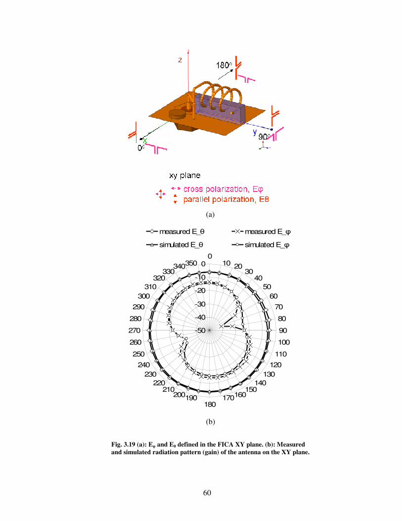
60
Fig. 3.19 (a): Eφ and Eθ defined in the FICA XY plane. (b): Measured
and simulated radiation pattern (gain) of the antenna on the XY plane.
-50
-40
-30
-20
-10
00
10 2030
40
50
60
70
80
90
100
110
120
130
140150
160170180
190200210
220
230
240
250
260
270
280
290
300
310
320330
340350
measured E_θ measured E_φ
simulated E_θ simulated E_φ
(a)
(b)

61
The co-polarized gain was recorded with the FICA’s feeding and shorting pins
parallel to the λ/2 dipole, which is plotted as Eθ in the XY plane of Fig 3.193. The
FICA is cross-polarized when these two pins are perpendicular to the transmit dipole.
The cross-polarized gain pattern is plotted as Eφ in the XY plane in Fig. 3.19. Since
the gain pattern is measured in dBd, the far-field electric field magnitude gain pattern
(Eθ and Eφ) and the power gain pattern are the same in decibels.
From Fig. 3.19, we can make two observations. First, the antenna has much
higher gain for the co-polarization than for the cross-polarization. Second, FICA gain
in co-polarization has a uniform pattern, like a short dipole. The helix radiation
pattern shows directivity characteristics. Similar results were obtained through HFSS
simulation and are also plotted in Fig. 3.19.
The above observation can be explained using image theory. For an electrical
current over a ground plane, the ground plane can be replaced by an equivalent image
current located an equal distance below the ground plane. The image current has the
same direction for an electrical current perpendicular to a ground plane, and has the
opposite direction for an electrical current parallel to the ground plane, as shown in
Fig. 3.20 (a).
3 Eθ and Eφ are normalized to the (λ/2 dipole) co-polarized and cross-polarized electric field in
the far field. Co-polarized and cross-polarized are terms used in [Stutzman98].

62
As can be seen in Fig. 3.14, currents in the two vertical pins (feeding pin and
shorting pin in Fig. 3.14) flow in the same direction. Their image currents also flow in
the same direction. This enhances the radiation in co-polarization. For the helical part,
each winding can be approximated as a small loop. As can be seen in Fig. 3.20 (b),
for a small loop, currents and image currents in all directions cancel out. Due to the
imperfections and limited size of the ground plane, the weak net current of the helix
contributes to the weaker cross polarized radiation, as shown in Fig. 3.21. Therefore,
currents flowing in the two vertical pins (the feeding and the shorting pin) are
radiating more efficiently than the current flowing in the helical part of the antenna.
This is proved by measurements, and was predicted in section 3.4.3 and shown in Fig.
3.14.
Vertical electrical current
Horizontal electrical current
Image current
Electrical current on a small loop
Image current
(a) (b)
Fig. 3.20 Image current. (a): Image current of vertical and horizontal electrical current
over a ground plane. (b): Image current of electrical current on a small loop over a
ground plane.

63
From Fig. 3.19, the measured peak gain of the FICA is -3.53dB lower than a
standard half wave dipole, whose directivity is 1.641. Using the directivity of a small
dipole (=1.5), the efficiency η of FICA is calculated as follows:
72796.0641.1*10 353.0 ≈= −FICAG , (3.6)
%53.485.1
72796.0≈=≡
yDirectivit
Gainη . (3.7)
Considering that the total volume occupied by this FICA, including the
ground plane, is only 0.024λ × 0.06λ × 0.076λ, this small antenna is very efficient.
The performance comparison of this work with other ESAs is summarized in Table
3.1. The volume of the other ESAs is too big to fit into a SDWSN transceiver node.
The total volume of the FICA in this work is only 7% of other ESAs.
Fig. 3.21 Electrical current and its image current along the helix of FICA.

64
Table 3.1 Antenna Performance Summary (NA=not available)4
[Choo05] [Chen05] [Ojefors05] This work
#1 This work
#2 This work
#3
Type of ESA Genetic Algorithm
PIFA IFA IFMLWA (section 3.4.2.1)
FICA 1 (section 3.4.2.2)
FICA2 (section 3.4.2.3)
Ground plane size
0.11 λ ×
0.11 λ
0.2 λ ×
0.26 λ
0.176 λ ×
0.208 λ
0.08 λ ×
0.12 λ
0.06 λ ×
0.076 λ
0.06 λ ×
0.076 λ
Antenna Height
0.11 λ 0.026 λ 0.04 λ 0.024 λ 0.021 λ 0.024 λ
Antenna Volume
1.3×10⁻³ λ3 1.4×10⁻³
λ3
1.7×10⁻³ λ3 2.23×10⁻⁴
λ3
1×10⁻⁴ λ3 9×10⁻⁵ λ3
Bandwidth 2.1% (-3dB)
2.26% (-10dB)
8.3% (-10dB)
4.4% (-10dB)
1.6% (-10dB)
2.45% (-3dB)
Gain (dBi) NA 0.75 -0.7 NA NA -1.38
Efficiency 84% NA 52% NA NA 48.53%
Operating frequency
(MHz)
394
1946
2400
916
916
916
3.4.6 Antenna on a Live Radio
We have utilized this antenna in a real “Smart Pebble” node. The performance
of the proposed low profile, small volume FICA antenna was tested through
communication range measurements with a custom-designed application-specific
WSN implemented in the DSPCAD (Digital Signal Processing Computer-Aided
Design) research group at University of Maryland [Shen07]. A Chipcon CC1110
[CC1110] at 916MHz is the core of the transceiver device. On each WSN node we
integrated a microphone sensor, an antenna, a transceiver circuit, and a battery. All
components are stacked together as depicted in Fig. 3.22.
4 [Choo05] does not provide gain, and [Chen05] does not provide efficiency. Therefore, there
are NA entries in this table. For IFMLWA and FICA1, we did not have the opportunity to measure the gain and efficiency. Therefore, these numbers are absent from Table 3.1.
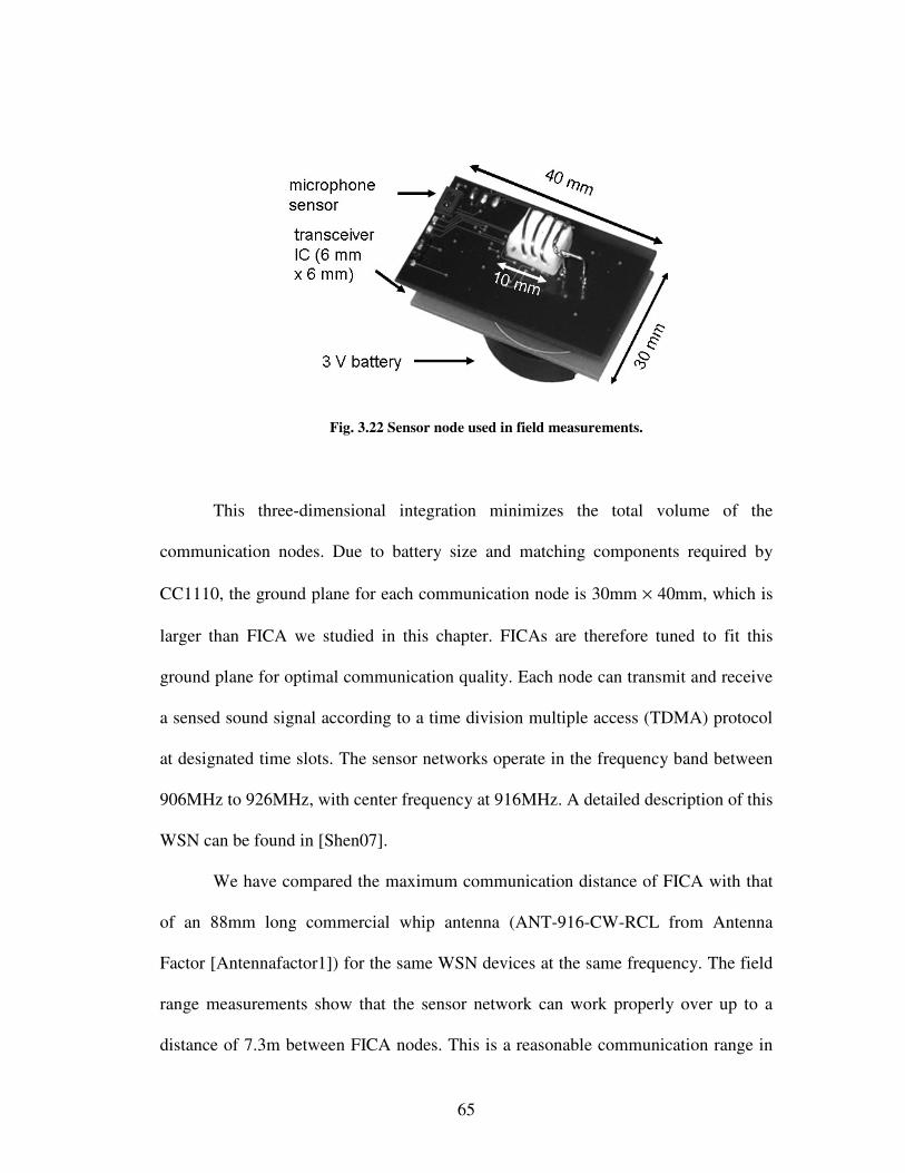
65
This three-dimensional integration minimizes the total volume of the
communication nodes. Due to battery size and matching components required by
CC1110, the ground plane for each communication node is 30mm × 40mm, which is
larger than FICA we studied in this chapter. FICAs are therefore tuned to fit this
ground plane for optimal communication quality. Each node can transmit and receive
a sensed sound signal according to a time division multiple access (TDMA) protocol
at designated time slots. The sensor networks operate in the frequency band between
906MHz to 926MHz, with center frequency at 916MHz. A detailed description of this
WSN can be found in [Shen07].
We have compared the maximum communication distance of FICA with that
of an 88mm long commercial whip antenna (ANT-916-CW-RCL from Antenna
Factor [Antennafactor1]) for the same WSN devices at the same frequency. The field
range measurements show that the sensor network can work properly over up to a
distance of 7.3m between FICA nodes. This is a reasonable communication range in
Fig. 3.22 Sensor node used in field measurements.

66
SDWSNs (Chapter 2). By using the commercial 88mm whip antenna, this distance is
improved only to 7.6m. These results show that the FICA is a good candidate for
compact communication nodes.
3.4.7 FICA Parametric Study
Input impedance, which indicates the matching conditions of an antenna, is an
important measure in antenna studies. FICA operates in a similar fashion as folded
dipoles as discussed in section 3.4.1. The correct matching is normally obtained
experimentally. The very good match between experimental and simulation results
shown in Fig. 3.17 and Fig. 3.19 provides us the confidence to try to boost the
performance of FICA through computer simulation tools. This section reports the
results of a FICA parametric study using HFSS. The object here is to evaluate the
effect of each geometric parameter on the antenna input impedance and optimize the
critical parameters for further experiments or prototype fabrication.
In the following, the size of the ground plane is selected to be that of the final
antenna: 25mm by 20mm. The ground plane size effect is discussed in section 3.5.
Parameters such as wire diameter, coil spacing, major and minor radius of the coils,
number of turns, vertical pin height, bending position, and bending angle are studied
in this section. Some of the above parameters are depicted in Fig. 3.23. Symbol
definitions and default values of all studied variables are listed in Table 3.2.

67
Table 3.2 Variables used in parametric simulation.
Symbol Corresponding parameter Default Value
φ (degree) Feed Angle (Refer to Fig. 3.23) 80
θ (degree) Tap Angle (Refer to Fig. 3.23) 60
h1 (mm) Feeding Pin Height (Refer to Fig.3.23) 4
d1 (mm) Pin Distance (Refer to Fig. 3.23) 7
s (mm) Coil Spacing 3
AD (mm) Major Diameter of Coil 4
BD (mm) Minor Diameter of Coil 3
N Number of Turns of Coil 3.6
3.4.7.1 Feeding Structure Parametric Study
We first study the parameters that are most sensitive to the matching condition
and antenna input impedance, such as h1, d1, θ, and φ (Table 3.3). Table 3.3
summarizes the resonance frequency versus sweeps of these parameters. Default
values in Table 3.2 are used for other parameters not swept in Table 3.3.
Fig. 3.23 Geometric representation of some analyzed parameters.

68
Table 3.3 Resonance frequency (fc) of FICA for different h1, d1, θ, and φ.
h1 (mm)
fc (MHz)
d1 (mm)
fc (MHz)
θ (degree)
fc (MHz)
φ (degree)
fc (MHz)
4 910 4 900 60 910 50 898
5 912 5 903 70 910 60 902
6 914 6 907 80 916 70 908
7 918 7 910 -- -- 80 910
From Table 3.3 and the simulation details, we make the following
observations:
1. The resonance frequency increases slowly with h1.
2. The resonance frequency increases with d1. We also observe that bandwidth
increases with d1 in simulations.
3. Increasing the tapping angle θ, so that the tapping point moves away from the
grounded end of the shorting pin, increases the resonance frequency, narrows
the bandwidth, and achieves better matching to 50Ω.
4. Increasing the feeding angle φ, so the Lexan block and the helix move closer
to the ground plane edge, increases the resonance frequency and has
negligible effect on the matching condition.
The above observations are helpful in finding an optimal tapping point during tests.
For example, to increase the resonance frequency slightly for a fixed helix geometry,
one should try to increase the length from the feeding end to the tapping point.
3.4.7.2 Helix Structure Parametric Study
The effect of the helical wire geometry is studied in this section. Different
values for the helix used in analysis are listed in Table 3.4.

69
Table 3.4 Values used in coil parametric study.
Coil major diameter : AD (mm)
Coil spacing: s (mm)
Number of coil turns: N
Length of this portion (mm)
2 2 5 80
2 3 5 80.76
2 4 5 81.9
3 2 4.2 79.6
3 3 4.2 80
3 4 4.2 81
4 2 3.6 80.1
4 3 3.6 80.5
4 4 3.6 81.1
5 2 3.1 79.8
5 3 3.1 80.2
5 4 3.1 80.6
6 2 2.7 79.1
6 3 2.7 79.4
6 4 2.7 79.7
7 2 2.5 81.9
7 3 2.5 82.1
7 4 2.5 82.4
We have adjusted AD, BD, N, and S simultaneously such that the total length
of the helix from the tapping point to the open end is roughly constant. Default values
in Table 3.2 are applied to unspecified variables. As can be seen in Fig. 3.24, the
resonance frequency slightly increases with coil spacing if the coil major diameter
AD is fixed. This can be explained intuitively. The inductive energy lost in the
environment increases with the helical coil spacing s, so the helix inductance drops
with s. As shown in Fig. 3.25, if we decrease the coil’s major diameter AD and fix the
coil spacing s, then N needs to be increased to keep the helix length unchanged. Figs.
3.24 and 3.25 also show that if the antenna is already matched to a desired load (i.e.,
50 Ohms) at a frequency close to the operating frequency, adjusting the coil shapes
and turns will have a minimal effect on the matching condition.
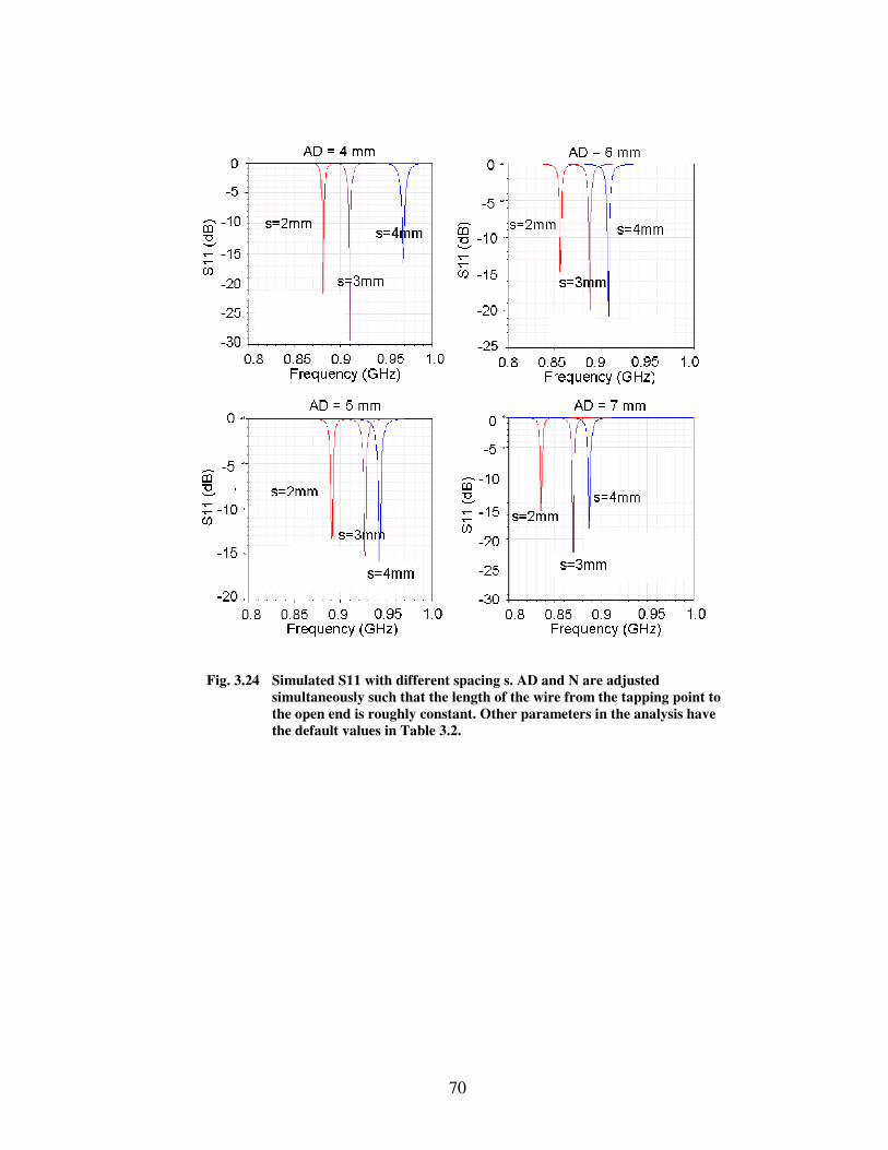
70
Fig. 3.24 Simulated S11 with different spacing s. AD and N are adjusted
simultaneously such that the length of the wire from the tapping point to
the open end is roughly constant. Other parameters in the analysis have
the default values in Table 3.2.

71
The above feeding and helical structure parametric studies provide designers
with very useful information on antenna tuning. Different helix structures should have
very similar tapping and feeding positions at the same frequency of interest. Tapping
angle θ, feeding pin height h1, and pin distances d1 are critical parameters that
determine the antenna input impedance matching.
3.5 Ground Plane Effect for ESA and FICA
The electromagnetic coupling between the current in ESA wires and the PCB
induces surface currents on the ground plane. As stated before, using the ground
Fig. 3.25 Simulated S11 with different major diameters for the coil and s = 2mm.
AD and N are adjusted simultaneously such that the length of the wire
from the tapping point to the open end is roughly constant. Other
parameters in the analysis have the default values in Table 3.2.

72
plane as part of the antenna to provide a return current for monopole-type antennas is
a common way to reduce their size. Nevertheless, most existing studies only focus on
ground plane size larger or close to a quarter wave length, and rarely examine
antennas whose ground planes are smaller than 1/10λ, or even less than 1/4λ. This
section studies this ground plane effect and shows:
(1) The ground plane indeed plays a very important role in antenna gain.
(2) A FICA with a much smaller ground plane outperforms commercial chip
antennas.
Fig. 3.26 is a photograph of a 916MHz chip antenna [Antennafactor2]
assembled to ground planes of different sizes. According to the manufacturer, the
antenna performs well when at least one edge of the PCB is of one quarter wave
length. The antenna should be located in an area free of the ground plane and fed by
microstrip lines, as shown in Fig.3.26 (#1). This requirement further increases PCB
size for chip antennas. Table 3.5 summarizes the measured gain of antennas in each
case. To compare their performance with FICA, the gain of the FICA in section
3.4.2.3 is listed in the last column. All antennas in Table 3.5 have an omnidirectional
radiation pattern, and directivity of around 1.5. According to Table 3.5, the ground
plane of FICA is only 12% of that in PCB1, while its gain is 4.36dB higher than the
one in PCB1. Reducing the ground plane size to PCB3, in which the metal portion of
PCB is smaller than λ/4, reduces the gain by 5.7dB compared to the chip antenna in
PCB1, and by 10.06dB compared to the FICA. In addition, the ground plane of PCB3
is still more than 7 times larger than that of the FICA. Therefore, FICA has much
better performance than chip antennas in terms of gain and ground plane size.

73
Table 3.5 Gain of chip antenna assembled on different PCBs.
Construction Chip antenna on PCB 1
Chip antenna on PCB 2
Chip antenna on PCB 3
FICA in section 3.4.2.3
PCB size 0.11λ × 0.34λ 0.11λ × 0.27λ 0.11λ × 0.21λ 0.06 λ × 0.076λ
Antenna Gain (dBi)
-5.74 -10.24 -11.44 -1.38
3.6 FICA Circuit Model
In communication circuit design, there is a need to model antennas as lumped
circuits during the earliest design stage, if possible. This increases the design
efficiency, reduces the design cycle, and most importantly, it provides more freedom
in antenna and system optimizations, such as in antenna-LNA-PA co-design (chapter
5).
A common way to determine the antenna circuit model is to directly measure
the S parameters of the antenna, and then use optimization tools to fit measured data
Fig. 3.26 Commercial 916 MHz chip antenna assembled on PCBs
of different sizes. From left to right: Chip antenna on PCB1; Chip
antenna on PCB2; Chip antenna on PCB3.

74
to a Foster network [Wang05] or a variant thereof. However, it is not unusual to find
negative resistor values, which do not have physical meanings, from the purely
mathematical curve fitting method [Kajfez05]. Authors in [Dejean07] demonstrated a
nonsystematic method to invert curve-fitted negative resistors into positive
counterparts, although the method is not a physics-based approach.
In this section, we derive a remarkably simple and accurate circuit model of
FICA that has the following advantages:
1. This circuit model provides great convenience in antenna-circuit interface
designs.
2. This physics-based circuit model only needs the information of two measured
impedances, and requires no complex optimization tools.
3. The antenna efficiency is embedded in the circuit components of this model.
4. It explains FICA impedance matching from an equivalent circuit point of view.
It is straightforward to build the equivalent circuit by observing the physical
construction of the FICA in Fig. 3.27 (a).
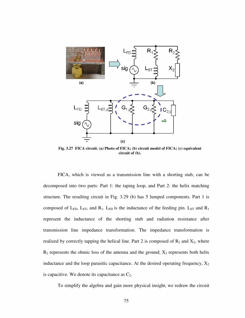
75
FICA, which is viewed as a transmission line with a shorting stub, can be
decomposed into two parts: Part 1: the taping loop, and Part 2: the helix matching
structure. The resulting circuit in Fig. 3.29 (b) has 5 lumped components. Part 1 is
composed of LFD, LST, and R1. LFD is the inductance of the feeding pin. LST and R1
represent the inductance of the shorting stub and radiation resistance after
transmission line impedance transformation. The impedance transformation is
realized by correctly tapping the helical line. Part 2 is composed of R2 and X2, where
R2 represents the ohmic loss of the antenna and the ground; X2 represents both helix
inductance and the loop parasitic capacitance. At the desired operating frequency, X2
is capacitive. We denote its capacitance as C2.
To simplify the algebra and gain more physical insight, we redraw the circuit
Fig. 3.27 FICA circuit. (a) Photo of FICA; (b) circuit model of FICA; (c) equivalent
circuit of (b).
(a) (b)
(c)
=G

76
in Fig. 3.27 (b) to its parallel equivalent circuit in Fig. 3.27 (c). This is done directly
by series to parallel transformation. For example, 11 / RLQ STω= is the quality factor
of the STLR ,1 branch. For low loss material, Q1 is high. Therefore,
( ) STSTpST LQLL ≈+⋅= −2
1, 1 , (3.8)
( ) pp GRQR ,11
2
1,1 11 =+= . (3.9)
Here LST,p is the parallel equivalent inductance of LST. R1,p is the resistance of
conductance G1,p . A similar transformation can be applied to the R2--X2 branch,
where we denote the components as G2,p and C2,p in Fig. 3.27 (c).
It is well known in transmission line theory that we can match an open-ended
resonant transmission line to any impedance by tapping it with a short stub at the
right position along the transmission line. From (3.9), we observed that for larger Q in
resistance-reactance serial branch, resistance in a parallel equivalent circuit is much
larger than its serial counterpart. At resonance, all reactive components compensate
each other. Therefore, the real part seen from the source is this larger parallel
equivalent resistance. Therefore, the very small radiation resistance of a very short
dipole and the very small ohmic resistance of the wire can be matched to a much
larger impedance (i.e., 50Ω in our test). This explains the FICA impedance matching
from a circuit point of view.
The next step is to find the feed point impedance Zin and the value of each
component in Fig. 3.27 (b) based on FICA input impedance and gain measurements.
Without knowledge of gain or efficiency of the FICA, it is hard to
discriminate the conductance due to radiation and loss. Therefore, we combine these
two as pp GGG ,2,1 += to simplify the derivation. The input impedance is given by

77
the expression:
1
,2
,
,2,1
1−
++++= p
pST
ppFDin CjLj
GGLjZ ωω
ω (3.10)
1
,2
,
1−
+++= p
pST
FDin CjLj
GLjZ ωω
ω . (3.11)
If we define , 2,1/( )ST p p
Y L Cω ω= − , then
( )
)Im()Re(2222
22
1
ininFD
FDFDin
ZjZYG
YLj
YG
G
YG
jYGLjjYGLjZ
⋅+=
+++
+=
+
++=−+=
−
ω
ωω
. (3.12)
Here,
22)Re(
YG
GZ in
+= (3.13)
22)Im(
YG
YLZ FDin
++= ω . (3.14)
As we have discussed in section 3.4.5, the FICA reaches the high impedance
resonance point at frequency ω1 and low impedance resonance point at frequency ω2,
where ω1<ω0<ω2. Here, ω0 is the frequency where the antenna achieves the best
match. With the information of the impedance at ω1 and ω2 (Table 3.6), all circuit
components values can be retrieved.
Table 3.6 Measured FICA input impedance at resonance.
Frequency (Mrad/s) Re(Zin) (Ω) Im(Zin) (Ω)
ω1 = 2π × 911.5 150.52 0
ω2 = 2π × 921.88 22.073 0

78
At resonance, 0)Im( =inZ . From (3.13),
2
2
2
1
2
1G
LLY
FDFD
−
±−=
ωω . (3.15)
Using (3.14) and (3.12) gives
2
2
2
2
22
2
1
2
1
)Re(
−
±−+
=+
=
GLL
G
G
YG
GZ
FDFD
in
ωω
, (3.16)
and (3.15) is simplified to
[ ] [ ]0
)Re()Re(1
22
2
2
22
2
=−
+ G
L
ZG
L
Z
FD
in
FD
in
ωω . (3.17)
Since radiation and loss by the FICA cannot be zero, 0≠G . Therefore,
222)Re(
)Re(
FDin
in
LZ
ZG
ω+= . (3.18)
Given the value in Table 3.6, mSG 813.5= and nHLFD 93.9= . Therefore,
0021969.01
2
1
2
1,21
1
2
2
11
1 −=−=−
+−= p
FDFDFD
CL
GLL
Y ωωωω
, (3.19)
0151518.01
2
1
2
1,22
2
2
2
22
2 −=−=−
+−= p
FDFDFD
CL
GLL
Y ωωωω
. (3.20)
Solving (3.19) and (3.20), we have
nHYY
L pST 306.0
2
1
1
2
1221, =
−
−=
ω
ω
ω
ωωω
and pF
YY
C p 100
2
1
1
2
1
2
2
1
,2 =
−
−
=
ω
ω
ω
ωωω
.
The FICA input impedance, based on the above circuit values in Fig. 3.27 (c),

79
is plotted in Fig. 3.28. As one can see from Fig. 3.28, the FICA circuit model derived
from high impedance and low impedance resonance points matches measurements
very well.
We have applied this method to FICAs with ground planes of different sizes.
Again, the measured Zin matched the modeled Zin closely, as expected (Fig. 3.29).
Fig. 3.28 Measured Zin and modeled Zin. Ground plane size: 20mm ×××× 25mm.

80
3.7 Scaling FICA to Other Frequencies
The proposed FICA can be easily scaled to other frequencies. For example,
we have scaled FICA to 2.2GHz and 2.45GHz in order to work with the custom
designed 2.2GHz OOK DDR in this thesis and CC2430 transceiver module from TI
[CC2430]. We also have the flexibility to scale the design to lower frequencies, such
as the 433MHz ISM band, to work with a variety of commercial or prototype radios.
In this section, we will show that FICA performance for scaling to both higher and
lower frequencies.
The diagram and photograph for FICA scaled to 2.2GHz and to 2.45GHz is
shown in Fig. 3.30 panels (a) and (b), respectively.
Fig. 3.29 Measured Zin and modeled Zin.
Ground plane size: left: 60mm ×××× 75mm; right: 76.2mm ×××× 95.3mm.

81
In Fig. 3.30, the ground plane for FICA at 2.45GHz is only 0.09λ × 0.09λ. The
measured bandwidth for a 2.2GHz antenna is 40MHz at S11 = -3dB and 12MHz at
S11 = -10dB. To integrate the antenna into a full radio with sensor and batteries at
2.45GHz, a ground plane of 0.12λ × 0.12λ is used for the 2.45GHz FICA, which has a
bandwidth of 10MHz.
The radiation pattern of FICA at 2.45GHz and 2.2GHz were measured with
experimental settings similar to those in section 3.4.5. To reduce the current coupled
to the coaxial cable, and suppress the radiation induced by cables, baluns with 3
sections at 2.2GHz and 2.45GHz were used in all the measurements. Measurements
were performed both in an open field and inside an anechoic chamber. Similar results
were obtained with both methods. The radiation pattern of a 2.2GHz FICA measured
in the FDA anechoic chamber is shown in Fig. 3.31.
Fig. 3.30 Diagram (a) and photograph (b) of FICA at 2.2GHz and 2.45GHz.
z
x y

82
As it can be seen in Fig. 3.31, the FICA at 2.2GHz has a similar radiation
pattern as the one at 916MHz. However, the gain at 2.2GHz is lower, because the pin
height at 2.2GHz is much shorter (only 3mm). In addition, the contribution of
dielectric material loss increases with frequency. These effects lower the ratio of
radiation resistance to ohmic resistance. Therefore, this FICA appears to have lower
efficiency. The FICA at 2.45GHz is integrated to a full Smart Dust node with
CC2430 [CC2430] as the radio. The measured communication distance is 2m for
1mW transmitted power.
Fig. 3.32 shows the measured S11 for FICA scaled to 433MHz. This antenna
is used in an ISM radio for communications over 1km. A rough indoor test shows the
communication range of this antenna exceeds the size of the building (end to end
distance is 30 meters). It can be seen from the above data that a FICA scaled to lower
frequencies also significantly reduces the volume of the antenna. Since the 433MHz
Fig. 3.31 Measured gain of a 2.2GHz FICA. Left: Eφ and Eθ on XY plane. Right: Eφ and
Eθ on XZ plane. Coordinates are defined in Fig. 3.19 and Fig. 3.30.

83
band is not in the desired frequency range for SDWSN, we did not perform a full
analysis of this antenna, e.g., its radiation pattern measurements.
3.8 Conclusion
This chapter first reviews the state of the art for electrically small antennas
(ESAs), and then proposes design guidelines and goals for ESAs used in Smart Dust
Wireless Sensor Networks (SDWSN). The performance of a set of novel scalable low
profile ESAs —F-inverted compact antennas (FICA) with very limited ground plane
size and total volume— is presented. Special care to avoid artificial effects was taken
when designing and measuring the performance of the FICAs.
The novelty and advantages of the proposed FICA include:
(1) The device is designed to be used in low GHz SDWSN, where no
conventional ESAs can be applied directly. To the author’s best knowledge,
Fig. 3.32 Measured S11of FICA scaled to 433MHz.

84
no work on this topic has been reported in the literature. The FICA in this
thesis has worked very well within the strict volume constraints for Smart
Dust type wireless sensor networks.
(2) The operation principles of FICA differ from normal mode helix antennas.
The idea of applying a helix mainly as a low loss impedance matching
structure is first proposed in this work. This design simultaneously reduces the
volume of the ESA and the electromagnetic interference to the circuit
components integrated on the PCB. For a 916MHz FICA with a volume as
low as 9 × 10⁻⁵ λ
3, an efficiency as high as 48.53% is achieved.
(3) A remarkably simple FICA circuit model based on physics is derived. It
provides great convenience when used together with circuit simulators for
compact and energy efficient antenna/circuit co-design.
(4) The proposed FICA is frequency scalable. FICAs scaled to lower frequencies
(433MHz) or higher frequencies (2.2GHz) are presented in this chapter.

85
Chapter 4 Low Power Low Noise Amplifier
Optimization
This chapter presents a novel low power, cascode low noise amplifier (LNA)
optimization method. This procedure includes active device and input/output passive
matching network optimization. For active devices, an optimizing function gm / IDF is
used when optimizing active devices, where gm is the transconductance that is related
to gain, ID is the drain current of transistors that is related to power consumption, and
F is the noise factor of the transistors. Managing this performance function helps to
achieve optimized design. It is demonstrated through an analytical model and by
simulation tools that gm / IDF reaches its maximum value in the moderate inversion
region. For passive input and output networks, this thesis proposes a design
methodology for maximum voltage gain, which requires a high quality factor for
input networks, and high load impedance for output networks. In particular, this work
introduces a negative input impedance near the operating frequency due to the
resonance load impedance of cascode amplifiers. This negative impedance has proved
very effective in cancelling input network losses, improving the input network quality
factor (Q), and increasing the voltage gain and signal to noise ratio. Finally, using the
proposed active and passive component optimization technique, an efficient high

86
voltage gain cascode LNA has been designed and measured in a 0.13µm CMOS
standard digital process which uses only low Q inductors. This LNA has a noise
figure of 3.6dB, a voltage gain of 24dB, an input third order interception point (IIP3)
of 3dBm, and a power consumption of 1.5mW at Vdd = 1.0V. Its figure of merit is
twice that of the best in the literature due to the low power consumption.
This chapter is organized as follows: Section 4.1 reviews existing LNA design
methods, explores the LNA design space, and proposes the design goals. Section 4.2
provides a step by step cascode LNA active device optimization via modeling and
simulation. Section 4.3 proposes the voltage gain passive matching network design
method. Section 4.4 and section 4.5 study the input and output matching circuit
optimizations for a cascode LNA. Section 4.6 shows a design example. Section 4.7
concludes this chapter.
4.1 Introduction
4.1.1 Existing LNA Design and Optimization Methods
The first stage in nearly all receiver architectures is a low noise amplifier
(LNA), which determines the system noise level according to Friis’ chain theory
[Friis44]. A LNA is a power consuming circuit block due to noise suppression, gain,
and linearity requirements. Designing a LNA with about a 1mW power budget and
acceptable performance using a standard CMOS digital process without high Q
inductors is a very challenging task.
Two methods are widely adopted in power constrained LNA designs. The first
one selects an optimized transistor width that is a function of the operating frequency,

87
source impedance, transistor length, gate oxide capacitance, and optimized input
network quality factor [Shaffer97]. In this method, the transistor size is mainly
determined by the technology node, as long as it operates in strong inversion region.
However, analog circuits working in strong inversion region normally consume much
more current than those in moderate inversion or weak inversion region. The typical
transistor width based on this method is a few hundreds to a thousand µm, with
typical power consumption of 10 to 20mW. A design methodology for transistors
operating in weak or moderate inversion is needed for LNA’s consuming about 1mW.
The other method is based on the discovery that the biasing condition for a
MOSFET operating with minimum noise figure is independent of frequency and
technology node [Yao07]. According to [Yao07], the best biasing current per unit
transistor width is around 0.15-0.20mA/µm. This result is immune to temperature and
process variations on the gate length and threshold voltage. In addition, the maximum
unity gain frequency also occurs in the vicinity of this bias condition. Therefore, this
method suggests biasing transistors at a current density of 0.15-0.20mA/µm. To limit
the power consumption to about 1mW, the transistor width must be of the order of a
few tens of µm. However, it is well known that the noise sensitivity factor Rn is
inversely proportional to transistor width [Lee03]. Due to process and temperature
variations, transistors are likely to have very large noise figures for large Rn. To
maintain a low Rn, power consumption for this method is on the order of 20mW.
The two methods just described are effective in designing high performance
LNA when the power budget is around 10 to 20mW. However, a new LNA design
guideline is needed for a power budget around 1mW, as required by Smart Dust

88
Wireless Sensor Networks (SDWSN).
4.1.2 Cascode LNA Design Space Exploration
Before we discuss the proposed design and optimization method details, we
first explore the LNA design space in this section.
Linearity
LNA in this work is applied as the first stage in an On-Off Keying (OOK)
receiver, in which the linearity constraint is less important than in receivers using
frequency or phase demodulation methods. In addition, MOSFET models at high
frequencies have largely increased complexity, while providing little information on
transistor biasing and sizing under low power constrains. To simplify the modeling,
nonlinearity effects are not included in this work.
Gain
Unlike power gain LNA designs, we focus on maximizing voltage gain in this
work, which we prove to be more effective for integrated circuits (section 4.3). The
maximum voltage gain is determined by the transistor intrinsic gain gmro, where gm is
the transistor’s transconductance and ro is the transistor’s output resistance. Both
values are functions of the transistor width W and the biasing VGS. VGS is the gate
source voltage of input transistors.
Power Consumption

89
Power consumption is determined by the product of the biasing current and
the supply voltage. For a 0.13µm CMOS technology, the supply voltage is 1.0V to
1.2V. Given the supply voltage, the power consumption solely depends on current
consumption. For a CMOS transistor, this current is mainly its drain current ID, which
is also a function of the width W and the biasing VGS.
Noise
It is well known that the drain current noise and the gate induced noise are the
major noise sources in a MOSFET [Ziel70]. To provide a simplified solution, we
neglect the gate induced noise and the noise source correlations to first order
approximation. The noise factor F of an intrinsic transistor is approximately (The
derivation of (4.1) is in Appendix A):
221 gss
msm
CRgRg
F ωα
γ
α
γ++≈ , (4.1)
where Rs is the source impedance which is independent of W and VGS. Cgs is the gate
source capacitance, which is a function of W. ω is the operating angular frequency,
which is 2π2.2GHz in this work5. γ is a fitting constant that has a value of unity at
zero VDS (drain source voltage) and decreases toward 2/3 for long channel devices in
saturation. For short channel devices, γ is 1-2[Lee03]. For cascode transistors, the
noise contribution of the common gate stage is minimal compared to the common
source stage. Therefore, although equation (4.1) is derived for common source
amplifiers, it is a good approximation for a cascode structure. According to (4.1), if Rs
and ω are fixed, F is a function of W and VGS.
5 For wideband LNA designs, ω should also be an optimization factor.

90
From the above discussion, gain, power, and noise are major concerns in LNA
design. LNAs should be designed for high voltage gain gmro, low power consumption
VddID (Vdd is a constant), and low noise figure F. Therefore, it is natural to define a
formula of gmro/IDF, which is a function of transistor size W and biasing VGS. In
section 4.2, analytical models for gmro/IDF are derived. Optimum W and VGS are
evaluated through an analytical model and using simulation tools. Optimization
methods for passive input and output matching networks are discussed in section 4.3.
The proposed LNA design flow is plotted in Fig. 4.1.
4.2 Optimizing Low Power LNA Sizing and Biasing
4.2.1 Cascode LNA Transistor Optimization Modeling
Describing transistor DC performance for short channel devices is very
challenging. The well accepted BSIM3 and BSIM4 [BSIM] models are empirical and
require hundreds of parameters. The subthreshold exponential model and the square
law model describe transistors in the subthreshold region and strong inversion region
Fig. 4.1 Design flow of low noise amplifier (LNA).
Active Circuit
(W, VG)
Input Passive
Matching Circuit
Best Intrinsic Performance (Gain, Power, Noise)
Best Overall Performance (Gain, Power, Noise)
Output Passive
Matching Circuit

91
well, but they require curve fitting in transition regions. To investigate intrinsic
transistor performance over the entire operating region, including the weak inversion,
moderate inversion, and strong inversion regions6, this work uses the EKV model
[EKV95]. The EKV model is a charge sheet model, requires very few parameters,
works well across all operating regions with a single closed form equation, and is
efficient for quick calculations.
The drain-source current in the EKV model can be approximated as
[Shameli06]:
( )TTHGS nUVV
oxTD eCL
WnUI
2/)(22 1ln2 −+= µ , (4.2)
where UT is the thermal voltage, n is the subthreshold slope factor which varies
between 1.1 to 1.9, and µ is the carrier mobility. The effective µ is approximated as
[Liu01]:
6.1
5
2
/106.61
/670
×+
=
cmV
E
Vscm
normal
effµ , (4.3)
ox
THGSnormal
t
VVE
6
+≅ . (4.4)
Enormal is the average normal electric field that emerges from the gate and terminates
at the channel charges and the bulk charges [Liu01]. tox is the gate oxide thickness. In
the EKV model, the transistor operation region is determined by transconductance
efficiency gm/ID versus an inversion coefficient IC. IC is defined as the ratio of drain
6 In the EKV model, the weak inversion region approximately corresponds to the subthreashold
region in the traditional MOSFET operation terminology, the strong inversion region approximately corresponds to the saturation region in traditional MOSFET operation terminology, and the moderate inversion region corresponds to the MOSFET transition region.

92
source current and the specific current of the transistor IS:
22 ToxS UL
WCnI µ= , (4.5)
SD IIIC /= . (4.6)
Correspondingly, a closed form gm/ID is derived as [Shameli06]:
141
21
++≈
ICnUI
g
TD
m . (4.7)
We plot a typical gm/ID ~ IC curve for a 0.13µm CMOS process in Fig. 4.2 (a)
to determine the transistor operation regions. Roughly speaking, gm/ID only depends
on the biasing condition, but not transistor size. The relationship of the operation
region in terms of the biasing condition is mapped into a VGS ~ IC plot in Fig. 4.2 (b).
As can be seen from Fig. 4.2 (a), the transistor operates in a moderate inversion
region when IC is around 1, in a weak inversion region when IC is much less than
0.1, and in a strong inversion region when IC is much greater than 10. From Fig. 4.2
(b), a transistor operates in the moderate inversion region when VGS is between 0.33V
to 0.75V. According to Fig. 4.2 (a) and (b), biasing transistors in the lower end of the
moderate inversion region are best for achieving high transistor transconductance
efficiency gm/ID. In this sense, a transistor is best biased between 0.33V to 0.48V.

93
From section 4.1.2, formula (4.8 a) is an object function for an optimization
problem. Optimum transistor sizing and biasing are defined as those values providing
maximum obj(VGS,W):
)()(
)()()(
,,
,,
,WVFWVI
WVrWVgWVobj
GSGSD
GSoGSm
GS = . (4.8 a)
The output resistance ro of short channel devices is higher in the weak and moderate
inversion regions than in the strong inversion region. To first order approximation,
the complicated ro is neglected, which will not affect the result. The object function is
then reduced to (4.8 b):
)()(
)()(
,,
,
,WVFWVI
WVgWVobj
GSGSD
GSm
GS = . (4.8 b)
The global or local maximum value of obj(VGS,W) can be found by solving (4.9):
=∂
∂
=∂
∂
0),(
0),(
W
WVobj
V
WVobj
GS
GS
GS
. (4.9)
(a) (b)
Fig. 4.2 (a) gm/ID ~ IC plot for 0.13µm CMOS. (b) VGS ~ IC plot for 0.13µm CMOS.
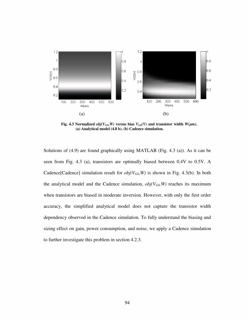
94
Solutions of (4.9) are found graphically using MATLAB (Fig. 4.3 (a)). As it can be
seen from Fig. 4.3 (a), transistors are optimally biased between 0.4V to 0.5V. A
Cadence[Cadence] simulation result for obj(VGS,W) is shown in Fig. 4.3(b). In both
the analytical model and the Cadence simulation, obj(VGS,W) reaches its maximum
when transistors are biased in moderate inversion. However, with only the first order
accuracy, the simplified analytical model does not capture the transistor width
dependency observed in the Cadence simulation. To fully understand the biasing and
sizing effect on gain, power consumption, and noise, we apply a Cadence simulation
to further investigate this problem in section 4.2.3.
(a) (b)
Fig. 4.3 Normalized obj(VGS,W) versus bias VGS(V) and transistor width W(µm).
(a) Analytical model (4.8 b). (b) Cadence simulation.

95
4.2.2 Systematic Investigation of Transistor Sizing and Biasing
To capture transistor higher order effects, we systematically investigate
transistor sizing and biasing following the design flow proposed in Fig. 4.4. Gain,
power, and noise requirements need to be satisfied.
Step 1. Monitoring IGE with respect to W at a specified VGS.
We sweep transistor width W while monitoring intrinsic gain efficiency (IGE
= gm1(gm2ro1ro2 + ro1 + ro2) / ID) for cascode transistors in a Cadence DC simulation.
As can be seen from Fig. 4.5, cascode transistor IGE decreases exponentially in the
moderate inversion region with increasing W. Transistors biased within the strong
inversion region have much lower IGE. This agrees with our prediction using the
simple analytical model in section 4.2.2. According to Fig. 4.5, a transistor width
Fig. 4.4 Design flow for transistor biasing and sizing in Cadence simulation. Intrinsic Gain Efficiency: IGE = gm1(gm2ro1ro2 + ro1 + ro2) / ID. Intrinsic Gain: IG = gm1(gm2ro1ro2 + ro1 + ro2).

96
smaller than 200µm is selected to obtain a high IGE based on these results. To check
the noise performance, we perform a SpectreRF simulation in step 2.
Step 2. Monitoring NF, NFmin, Rn while varying W at a specified VGS.
In step 2, we monitor cascode transistor intrinsic noise figure NF and noise
sensitivity factor Rn. To determine the target variable being monitored, effects of NF
and Rn are first estimated analytically. The noise effect of the transistor in the
common gate stage is neglected to simplify the problem. Using two-port noise theory,
the well known intrinsic NMOS transistor noise is modeled as [Lee03]:
( ) 22
min 15
21 LcC
gF gs
m
∝−+= γδω
(4.10)
W
L
gR
m
n ∝=α
γ (4.11)
( ) WLcCG gsopt ∝−=2
15γ
δαω (4.12)
VG1 = 0.46V, VDD = 1.2V
VG1 = 0.40V, VDD = 1.2V
VG1 = 0.80V, VDD = 1.8V
Moderate Inversion
Lower End of Moderate Inversion
Strong Inversion
Fig. 4.5 Cascode transistor intrinsic gain efficiency vs. W at different gate
biasing levels.

97
WLcCB gsopt ∝
+−=
γ
δαω
51 (4.13)
( ) ( )[ ]22
minmin optsopts
s
n BBGGG
RFFF −+−+=∆+= . (4.14)
In (4.10), Fmin is the minimum achievable noise factor of an intrinsic NMOS. δ is a
process related factor, which is normally 2γ. c is the correlation factor between drain
current noise and gate induced noise. Typically c = 0.395. Other parameters in (4.10)
were defined previously. From (4.10), the minimum achievable noise factor is
proportional to the square of the transistor length. From (4.11), Rn for an intrinsic
NMOS is inversely proportional to the transistor aspect ratio. (4.12) and (4.13) give
the optimum source conductance Gopt and optimum source susceptance Bopt for the
minimum noise factor. These two variables are proportional to the transistor area. The
overall noise factor of an intrinsic transistor is shown in (4.14), where Gs is the
conductance and Bs is the susceptance of the source admittance, respectively. To
obtain a low noise factor, both the minimum achievable noise factor Fmin and the
noise sensitivity factor Rn must be small. Therefore, we need to monitor both these
values when determining the optimum transistor size and bias. By recasting (4.14) as
(4.15),
( )222
minmin 2 optopt
s
nopt
s
soptn
s
ssn BG
G
RB
G
BGR
G
BGRFFF ++
+−
++=∆+= , (4.15)
we observe that the first and third terms are proportional to L2. The second term is
proportional to L/W. The last term is proportional to WL3. Therefore, we use a
minimal L for transistors in the cascode LNA design to achieve a low noise factor.

98
Eq. (4.15) also indicates that the transistor width has an optimum value since F
depends on both 1/W and W.
Fig. 4.6 shows the simulated noise figure NF (in dB), the minimum noise
figure NFmin (in dB), and the noise sensitivity factor Rn for cascode transistors in
weak inversion region, and moderate inversion region with two different gate-source
voltage levels. In weak inversion, intrinsic NFmin is much higher, and the unity gain
frequency fT is much lower. Therefore, optimum sizing and biasing should be
achieved by studying these two moderate inversion regions. In these regions, NFmin
increases with W, and Rn decreases with W. As a result, intrinsic NF reaches a small
value when W is 100-200µm. Further increasing W only decreases NF negligibly,
while power consumption increases linearly.
The previous discussion indicates that transistor with VGS close to the
threshold voltage and W of 100-200µm is a good starting point for an ultra low
power, low noise amplifier design. By comparing the Wopt results from the DC
simulation in step 1 and the SpectreRF simulation in step 2, we observe that Wopt
roughly falls in the same range. After the optimum width selection, we next study the
biasing effects on gain, power consumption, and noise. In this study, W is chosen to
be 100µm for low power consumption.

99
Step 3. At Wopt, monitoring IGE and IG while varying VGS to obtain VGS,opt.
To find the optimum biasing point, we first monitor the cascode transistor IGE
over a large bias range. Fig. 4.7 (a) shows that IGE decreases exponentially as the
Fig. 4.6 NF, NFmin, and Rn vs. W for cascode transistors. Top: Weak inversion region. Middle: Moderate inversion region. Bottom: Moderate inversion region with higher VG1.

100
transistor biasing voltage increases. However, transistor unity gain frequency is not
sufficiently large for a 0.13µm process in the subthreshold region for RF applications.
Transistors operating in subthreshold region should be avoided. Therefore, we must
obtain additional information to determine the appropriate bias range. As one can see
from the transistor’s IG plot (IG=gm1(gm2ro1ro2+ ro1+ ro2)) in Fig. 4.7 (b), IG is highest
when VGS is between 0.4V to 0.5V. According to Fig. 4.2, transistors operate in
moderate inversion at this bias level. Similar to the Wopt in steps 1 and 2, a SpectreRF
simulation needs to be performed to check the noise behavior at this biasing level,
which is discussed in step 4.
Step 4. At Wopt, monitoring F, Fmin, and Rn while varying VGS to obtain VGS,opt.
NF, NFmin, and Rn are monitored over variations of VGS in this step. From Fig.
4.8, both the minimum achievable noise figure NFmin and noise sensitivity factor Rn
reach a minimum when transistors are in moderate inversion, regardless of supply
Fig. 4.7 (a) Intrinsic gain efficiency (IGE) and (b) intrinsic gain (IG) of cascode transistors vs. VG1 at different supply voltage levels. Transistor sizes are W/L=100/0.12µm.
(a) (b)
IGE = gm1(gm2ro1ro2+ro1+ro2)/ID IG=gm1(gm2ro1ro2+ro1+ro2)IGE = gm1(gm2ro1ro2+ro1+ro2)/ID IG=gm1(gm2ro1ro2+ro1+ro2)

101
voltages. Therefore, NF is at minimum and robust to noise source impedance levels in
moderate inversion. Biasing transistors in the moderate inversion region indeed helps
to improve the noise figure while maintaining a high intrinsic gain (IG).
At this point, we have investigated and determined transistor optimum width
W and optimum biasing VGS at different supply voltage levels based on Cadence
simulation. Noise performance is also a strong function of transistor finger width and
the number of fingers for wide transistors. Therefore, the last step in active device
biasing and sizing optimization is to determine these values.

102
Step 5: Monitoring F, Fmin, Rn to determine optimum finger width.
As can be seen in Fig. 4.9, transistor finger width of 5-20µm is less noise
sensitive. Minimum NFmin occurs at a finger width of 5 to 10µm. Therefore, we select
a transistor width of 6µm, and an overall transistor width of 120µm in our low power
cascode LNA design. In the next section, we investigate the effect of input and output
0
1
2
3
4
5
6
7
8
0.2 0.4 0.6 0.8 1
VDD=0.8VVDD=1.0VVDD=1.2V
Wf=1µmx100
L=0.12µm
Rport1 = 50Ω
Rport2 = 10Ω
0
1000
2000
3000
4000
5000
6000
7000
0.2 0.4 0.6 0.8 1
VDD=0.8V
VDD=1.0V
VDD=1.2V
0
5
10
15
20
25
0.2 0.4 0.6 0.8 1
VDD=0.8VVDD=1.0VVDD=1.2V
Wf=1µmx100 L=0.12µm
Rport1 = 50Ω Rport2 = 10Ω
VG1 (V)
Wf=1µmx100
L=0.12µm
Rport1 = 50Ω
Rport2 = 10Ω
Fig. 4.8 Noise characteristics vs. VG1 at different supply voltage levels. Transistor
sizes are W/L=100/0.12µm. Top: Minimum achievable noise figure NFmin. Middle:
Noise sensitivity factor Rn. Bottom: Overall noise figure NF.
NFmin (dB)
NF (dB)
Rn (Ω)

103
matching networks.
4.3 Optimizing Matching Networks
4.3.1 Voltage Gain Oriented Design
There continues to be a long term debate over whether and how RF circuits
should be matched. To answer this question, we must clarify circuit requirements. For
example: (1) If optimal power transfer is important for the circuit, then load
impedance should be the complex conjugate of the source impedance. (2) If the noise
figure must be minimized (i.e., for a low noise amplifier), then the source impedance
needs to be optimized to achieve a minimal noise figure. (3) If long transmission
lines (i.e., the transmission line length is comparable to the minimum wavelength of
interest) appear on the printed circuit board or die, then proper matching (a.k.a.
“terminating”) must be applied to avoid reflections due to waves traveling back and
forth along the line. (4) If efficiency is important (i.e., for a power amplifier), then
impedance matching should favor the efficiency considerations rather than
Fig. 4.9 NFmin, NF, and Rn vs. transistor finger width. Transistor sizes are W/L=120/0.12µm. Biasing condition is VG1=0.46V. Supply voltage is 1.2V.

104
maximizing power transfer. In general, the resulting impedances for the above four
matching schemes are not equal. Therefore, we must balance performance and
matching trade-offs according to specific design requirements.
In our problem, signal lines on the die are much less than 1mm, much shorter
than the wavelength (about 136mm at 2.2GHz). Therefore we can ignore the
transmission line traveling effect and the question of proper termination on the chip
level7. In addition, the efficiency of the amplifier is more important for power
amplifiers than LNAs. Therefore, we only need to answer the question of whether an
ultra low power LNA needs noise matching and power matching networks, and how
to design them.
To discuss the power matching problem, let us first look at an example. Fig.
4.10 shows two LNAs with the same power consumption, input matching network,
transistor size, and biasing level. The output matching network is the only difference
between these two designs: LNA (a) is designed for maximum power gain. LNA (b)
is designed for maximum voltage gain. The input impedance of the RF source is 50Ω.
To compare power gain, both circuits are terminated with 50Ω loads. Simulation
results in Fig. 4.11 show that the power gain for LNA (a) (S21=17.5dB) is higher
than that of LNA (b) (S21=13.5 dB) at 2.2 GHz. To compare voltage gains, we load
both designs with a common source amplifier and current source load. Simulation
shows the voltage gain for LNA (a) (RFout/RFin =9.5V/V) is lower than that for LNA
(b) (RFout/RFin =15.83 V/V).
7 It is important to remember that if the input signal is fed through long coaxial cables or through long printed circuit board (PCB) lines, then the input power matching is still a concern.

105
In conclusion, amplifiers with higher power gain do not necessarily provide
high voltage gain. Typically, stages following LNAs are amplifiers or buffers. Inputs
of these acceding circuits are often MOSFET gate-source capacitors, not 50Ω loads as
in traditional RF circuits. To achieve higher SNR, a LNA passive network should be
designed for high voltage gain, not power gain. This work proposes a high voltage
gain oriented design, which is very important for on-chip low power LNAs.
LNA (a)
LNA (b)
Fig. 4.10 LNA cascaded with common source stage and current source load.
LNAs (a): Designed for maximum power gain, (b): for maximum voltage gain.

106
Then, why is power gain often used as a figure of merit for LNAs? This is
mainly due to historical and experimental reasons. Two decades ago, RF circuits and
(a)
(b)
Fig. 4.11 Simulated power gain and voltage gain of LNAs designed for high power gain or
high voltage gain. The difference of RF input in LNAs (a) and (b) is because the RF input is
the AC voltage from the gate of M1 to the ground, not from port1 to ground. Due to the
capacitive voltage amplification (section 4.4.1), these voltages differ slightly.

107
Millimeter Wave circuits were mainly built with discrete components. To cascade
different high frequency function blocks directly without worrying about reflection,
impedance matching is required for virtually all high frequency circuits with discrete
components [Gonzalez96]. From a measurement point of view, power gain is
measured when input and output are both matched to test cables (typically 50Ω).
Therefore, impedance matching and power gain are often important concerns in LNA
designs. However, voltage gain is more useful for evaluating the overall signal to
noise ratio (SNR) of the receiver, because digital output signals are measured by their
voltage levels. If LNAs do not drive a resistive load directly, at the same power
consumption, amplifiers with higher voltage gain tend to provide higher SNR than
those with higher power gain.
4.3.2 Voltage Gain and Noise Figure Trade-Offs
Practically, it is not possible to realize simultaneous noise matching and
voltage matching (or power matching) for most circuits, regardless of the power
consumption level [Shaeffer97][Nyugen05]. As explained in previous sections,
voltage gain is of more interest than power gain in the context of integrated circuits.
In this section, we discuss the trade-offs between noise matching and voltage
matching.
First, we derive the output SNR of a two-port network model in Fig. 4.12
(assuming Zs=Rs+j0):
( )[ ] ( )22
2
2222
222
SnnRS
in
vSnnRS
invout
RIVV
V
ARIVV
VASNR
++=
++=
α
α , (4.16)

108
where ( )sinin RZZ +=α is the voltage gain from the source to the input of the amplifier.
Zin is the input impedance of the noiseless network. Av is the gain of the noiseless
network. To maximize SNRout, Vin must be maximized while ( )22
SnnRS RIVV ++ should
be minimized. 2
RSV is the thermal noise of the source resistor. It is proportional to the
antenna radiation impedance and ohmic resistance. In this section, we assume 2
RSV is
fixed by the antenna design, and that circuit designers do not have the freedom to
change 2
RSV . The equivalent input referred noise sources of the amplifier is
( )2
Snn RIV + . From (4.16), for large Av, ( )2
Snn RIV + is small. This leads to higher
SNRout.
The noise factor can be viewed as the ratio of the total noise power at the
output to the noise power at the output due to source induced noise, as given by
equation (4.17):
Fig. 4.12 Two-port network for noise analysis.

109
2
22222
22
1
+=
+
==vns
namp
load
nampvns
load
vin
in
ns
in
in
out
in
Av
v
R
vAv
R
Av
R
v
R
v
SNR
SNRF . (4.17)
F is the noise factor, and SNRin and SNRout are the signal to noise ratios at input and
output, respectively. Av is the amplifier voltage gain; Rin and Rout are the input and
output impedances; vns is the source noise voltage; vnamp is the noise voltage of the
amplifier; vin is the input signal. From (4.17), the noise factor depends on voltage
gain, but not the load impedance of the amplifier.
Fig. 4.13 shows the simulated NF, NFmin, S22 of a cascode LNA for load
impedance Rload from 10Ω to 1MΩ. The load impedance mismatch is shown in Fig.
4.13 (b) by S22. From Fig. 4.13 (a), NF and NFmin collapse to a single curve for all
load impedance values when we keep the gain of the amplifier approximately the
same for all cases. From Fig. 4.13 (b), the load impedance indeed does not have a
good match unless it is around 50Ω. This load impedance independence agrees with
(4.17). We also observed (not shown in Fig. 4.13) that if we short Lg and C1, and then
vary the port impedance of port1 (Rport1), NFmin remains the same for all values of
Rport1, while NF varies significantly. This indicates that NF is sensitive to the input
matching network seen by the amplifier.

110
As a conclusion, NF strongly depends on the input impedance mismatch,
whereas it does not depend on the impedance at later stages at the same gain level.
Having high input network voltage gain helps to improve the noise figure, but
disturbs power matching. For on-chip systems, when designing passive networks,
input noise matching for achieving a low noise figure and high output voltage gain
are some dominant design goals.
4.4 Optimizing Input Matching Networks
4.4.1 Input Matching Network Design Guideline for Unilateral Circuits
From section 4.3, we understand that the input matching network is important
for obtaining a low noise figure, and the output matching network is important for
obtaining a high voltage gain. For classic cascode LNAs, input and output matching
(a) (b)
Fig. 4.13 (a) NF and NFmin for Rload=10Ω to 1MΩ. Curves for different Rload
values collapse into one NF and one NFmin plot. (b) S22(dB) for different values of
Rload. Since we only demonstrate the insensitivity of NF to Rload, the particular
Rload value for each curve in panel (b) is not important, and these are not labeled
due to space limitations.

111
circuits can be designed independently because cascode LNAs are stable and
unilateral in general. This provides great convenience to designers. However, cascode
LNA becomes bilateral at high frequencies if the load impedance is high. In this
section, we study the input matching network design guidelines for unilateral circuits.
In section 4.4.2, we discuss design guidelines for bilateral cascode LNAs.
First, we assume LNA in Fig. 4.13 (a) is unilateral and neglect the Miller
effect. The input impedance is 1gsin CjZ ω= ; ω is the angular frequency; Cgs1 is the
gate source impedance of transistor M1. To maximize the total voltage gain Av of the
LNA, the signal voltage drop Vin across Cgs1 should be maximized according to:
( )( )( )
( )( )ω
ω
ω
ωω
in
out
s
inv
V
V
V
VA ⋅= . (4.18)
In (4.18), Vs is the voltage of the generator, and Vout is amplifier output voltage.
The most commonly used matching network for a narrow band LNA can be
simplified as a LC series circuit (Fig. 4.14).
In Fig. 4.14, Rs is the source impedance of the generator. L and C are the
inductor and capacitor in the input matching network. Cgs1 is the gate source
impedance of transistor for LNA. The resonance frequency is given by:
Fig. 4.14 LC series circuit for LNA input matching network.

112
tot
oLC
1=ω , (4.19)
1
1
gs
gs
totCC
CCC
+= . (4.20)
The voltage across Cgs1 is:
( )
+×−=====
1111
1
gs
snet
sgso
s
ogso
s
gso
CgsinCC
CVjQ
RCj
V
jZCj
V
Cj
IVV
ωωωω. (4.21)
Z(jω0) is the impedance looking from the generator to the ground at resonance. Qnet is
the quality factor of the series network:
s
tot
s
o
stoto
netR
CL
R
L
RCQ ===
ω
ω
1. (4.22)
If Cgs1<<C, then Vcgs1 is Qnet times bigger than Vs at resonance. The passive
resonating circuit amplifies the AC voltage. To increase Vin=VCgs1, Qnet should be
high, which requires larger L, and smaller C, Cgs1, and Rs. The problem for high Q
input network is that the gate induced current noise is amplified by this Q factor
according to [Andreani01] and [Goo02]. Therefore, many designers choose Q to be
between 2 and 3. If the gate induced current noise is small, or if the noise bound is
loose, boosting input network Q is still an effective way to improve voltage gain. This
design perspective is especially useful when LNAs are used as cascade stages, in
which the input of LNA is the output of the previous stage, not from long test cables8.
Next, we study the methods for increasing input network Q. In section 4.4.2, we use
8 For long test coaxial cables, to avoid transmission line reflection effects, reasonable
impedance matching is still required at the input of the LNA to maintain the quality of the input signal.

113
negative input impedance to increase input network Q. In chapter 5, we use antenna
components to increase the input network Q.
4.4.2 Input Matching Network Design Guideline for Bilateral Circuits
Negative Input Impedance for Cascode Amplifiers
A cascode amplifier is widely accepted as a stable structure. However,
negative input impedance effects have never been studied deeply for cascode
amplifier design to the author’s best knowledge. In this section, we first derive the
negative input impedance for cascode amplifiers. Then, we propose circuit topologies
that use this negative impedance to improve input network Q, voltage gain, and noise
performance.
The analysis in section 4.4.1 is based on a simplified input circuit model for a
cascode LNA. However, at high frequencies the Cgd1 effect is no longer negligible.
Fig. 4.15 shows the small signal circuit of a cascode LNA with Cgd1. Parasitic
Fig. 4.15 Input impedance calculation for a Cascode LNA with LC tank load.
Cx = Cgb1 + Cgs2 + Cbs2, Cy = Cgd2 + Cdb2 + CL.

114
capacitors at the drain of M1 are lumped into Cx, where Cx = Cgb1 + Cgs2+ Cbs2.9
Parasitic capacitors at the drain of M2 are lumped into Cy, where Cy = Cgd2 + Cdb2+
CL. CL is the load capacitor from the drain of M2 to VDD. Fig. 4.16 is the small
signal circuit used for calculation. gm1 and gm2 are the transconductances of transistors
M1 and M2, respectively. Vt is a test source for the input impedance calculation. ro1
and ro2 are output impedances of transistors M1 and M2 stemming from channel
length modulation. These can also be represented by gds1 = 1 / ro1, gds2 = 1 / ro2, where
gds1 and gds1 are the drain-source transconductances of M1 and M2, respectively.
From Fig. 4.16, impedance looking up from the drain of M1 is Zx, where
x
dsL
dsm
dsdsm
x
CjgZ
ggggg
Z
ω++
+−+
=
−2
1
22222
1 . (4.23)
( ) )1//( yLdL CjRLjZd
ωω += is the load impedance. Because the gate of M2
is connected to the ground, via small signal circuit analysis, we can simply replace
gm2 with (gm2 + gmb2) in the above equation if the body effect is included. gmb2 is the
9 As a convention, the subscript of the capacitance indicates the two terminals of the capacitor
(g:gate, d:drain, b:body, s:source). The number is the transistor number that the capacitor belongs to.
Fig. 4.16 Small signal model for cascode LNA.
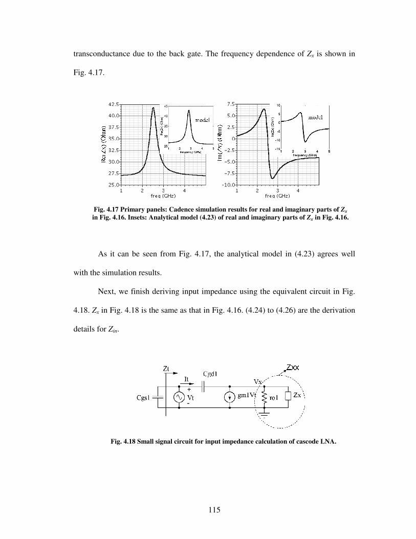
115
transconductance due to the back gate. The frequency dependence of Zx is shown in
Fig. 4.17.
As it can be seen from Fig. 4.17, the analytical model in (4.23) agrees well
with the simulation results.
Next, we finish deriving input impedance using the equivalent circuit in Fig.
4.18. Zx in Fig. 4.18 is the same as that in Fig. 4.16. (4.24) to (4.26) are the derivation
details for Zin.
Fig. 4.17 Primary panels: Cadence simulation results for real and imaginary parts of Zx
in Fig. 4.16. Insets: Analytical model (4.23) of real and imaginary parts of Zx in Fig. 4.16.
Fig. 4.18 Small signal circuit for input impedance calculation of cascode LNA.

116
1
1//
gs
tinCj
ZZω
= (4.24)
xxx ZrZ //01= (4.25)
( )xxmgd
xxgd
xx
m
xxgd
tZgCj
ZCj
Zg
ZCjZ
11
1
1
1
1
1
1
11
+
+=
+
+
=ω
ωω (4.26. a)
( )
+
+−++++−
++
+
+−++
=
2
22212111
2
1
2
22221
11
11
dsL
dsmdsdsmmgdxgd
xgd
dsL
dsmmdsds
t
gZ
ggggggCjCC
CCj
gZ
ggggg
Z
ωω
ω
(4.26. b)
Fig. 4.19 shows Zin according to (4.24) and from Cadence simulation. As can
be seen from Fig. 4.19, a negative real component of Zin appears near the tank load
resonance frequency. Though negative impedance may be harmful for amplifier
stability, it can also be helpful to cancel input network loss and increase the input
network Q and the overall voltage gain. For completeness, we next summarize three
negative input impedance compensation methods. However, we suggest the use of the
second method as it has the smallest chip area, as well as greater simplicity, and
confers extra benefits to the circuit noise figure and voltage gain.

117
Three Negative Input Impedance Compensation Methods
The negative resistance at the input of the LNA can be viewed as an
underdamping mechanism. Some losses (damping factors) can be added to the
amplifier to bring it back into the stable region. Loss can be introduced either 1) at the
output matching network, 2) at the input matching network, or 3) in the amplifying
path (i.e., via a source degenerated inductor).
1. Compensate negative Zin with output matching network
Negative Zin can be compensated by an output matching network. For
example, if the load of the amplifier is 50 Ω, then the resonant load feedback (through
Cgd1) to the input of the amplifier will be more “out of phase” and will decrease the
voltage amplitude observed at input. The small negative impedance at the input will
be compensated. The price paid is the smaller voltage gain at output. Therefore, this
method is not recommended for application in this work.
Fig. 4.19 Input impedance of cascode LNA with lossy LC resonance
tank. Primary panels: real and imaginary Zin from Cadence simulation.
Insets: analytical results according to (4.24).

118
2. Compensate negative Zin with input matching network
The input matching circuit preceding the amplifier usually has one or more
on-chip lossy spiral inductors. As we discussed in Fig. 4.14, this ohmic loss degrades
the Q of the input network and reduces the AC voltage drop across Cgs1, which
decreases the overall amplifier voltage gain. The negative component of Zin at input
can cancel this lossy component and increase voltage gain. This is a win-win
situation, wherein the circuit is stabilized by the inevitable loss, and the voltage gain
is enhanced.
Therefore, this work purposely designs a cascode LNA with a negative real
part of the input impedance to improve performance.
3. Compensate negative Zin with source degenerated inductor.
In conventional LNA designs, a source degenerated inductor Ls is used to
provide the 50Ω match to the real source impedance (Fig. 4.20). From a circuit
stability point of view, this inductor can be used to cancel the negative input
impedance induced by the out of phase voltage due to the high resonance load
coupled to the input. This second advantage is largely overlooked in the literature.
We use the following example to illustrate the negative input impedance cancellation
provided by Ls.
The circuit in Fig. 4.20 is used to calculate the impedance looking from the
gate of M1 for an amplifier with Ls. It is easy to find that Zx is the same as that in Fig.
4.16.

119
After simple algebra,
( ) ( )
( ) ( ) ( )A
gsCsC
AZ
gsCLCsCCs
A
ggsC
AZ
ggCLsLCs
i
vZ
mgdgd
x
mgdsgs
gdgs
dsmgd
x
dsmgss
sgs
t
tt
111111
2
11
111111
2
1
2 1
−−
⋅
−++
++
+⋅
+−
== (4.27)
1
1//
gs
tinCj
ZZω
= (4.28)
Fig. 4.21 shows the Cadence simulations of the input impedance (4.28) when Ls =
0.4nH. It is found that the negative input impedance is canceled by the positive real
component introduced by Ls in the input. The value of is positive real component is
approximately gmLs/Cgs, as derived by [Lee03]. The price paid is the area and ohmic
loss of Ls. The loss of Ls induces thermal noise and affects the SNR of the amplifier.
Fig. 4.20 Cascode LNA with source degeneration.

120
4.5 Optimizing Output Matching Circuit
According to our discussion in section 4.3: 1) Power matching is independent
of voltage gain; 2) Having a high voltage gain helps to improve the noise figure.
Therefore, the output matching network requirements can be summarized as: 1) No
complex conjugate matching circuit is necessary for maximum power transfer. 2) The
output circuit should be designed for maximum voltage gain. In this work, we use
output networks as in Fig. 4.10 (b). In addition, according to section 4.4, an output
circuit should provide negative input impedance around the operating frequency to
increase input network Q, reduce input network signal loss, and improve the LNA’s
voltage gain.
Fig. 4.21 Input impedance of Cascode LNA with Ls. Primary panels: real
and imaginary parts of Zin from Cadence simulation. Insets: real and
imaginary parts of Zin according to (4.28).

121
4.6 A 2.2GHz LNA Design Example
This section presents a 2.2GHz LNA design following the strategies proposed
in this chapter. The source impedance is assumed to be 50Ω, since the circuit is fed
by 50Ω cables during testing. The output is designed to drive cascading circuit blocks
and does not have best power match for 50Ω.
The LNA in this work uses 0.13µm IBM8RFLM technology, which has poor
quality inductors. Fig. 4.22 shows the simplified circuit, and Fig. 4.23 shows layout
and microphoto of this LNA. As can be seen from Fig. 4.24, the power gain of this
LNA is 11.3dB; the input reflection coefficient is -11.8dB; the output reflection
coefficient is -8dB. The input of the LNA has very good power matching. This is
necessary for this particular test setting (connected to a 50Ω cable). The P-1dB point
(one dB compression point) is -8dBm (Fig. 4.25). The simulated and measured noise
figures are shown in Fig. 4.26. Though not available in this CMOS technology, high
Q and low loss inductors can significantly improve the noise figure. The IIP3
measurements of a LNA operating at different VDD levels are shown in Fig. 4.27.
When supply voltage VDD = 1.2V, IIP3 = 5dBm. When VDD = 1.0V, IIP3 = 3dBm.
Fig. 4.22 Simplified 2.2GHz LNA schematic.

122
(a) (b)
Fig. 4.23 (a) Layout and (b) die microphoto of 2.2GHz LNA using a 0.13µm CMOS technology.
Fig. 4.24 Measured LNA S-parameters.

123
Fig. 4.25 Measured LNA P-1dB point.
0
0.5
1
1.5
2
2.5
3
3.5
4
1.9
1.9
4
1.9
8
2.0
2
2.0
6
2.1
2.1
4
2.1
8
2.2
2
2.2
6
2.3
freq (GHz)
NF
(dB
)
VDD=1.2V VDD=1.0V
`
Fig. 4.26 (a) Simulated and (b) measured noise figure for the LNA.

124
For digital circuits, this 0.13µm technology requires VDD = 1.2V, at which
the LNA power consumption is 2.16mW. If the analog and digital circuits use
different VDDs, i.e., the VDD for analog circuits is 1.0V, then the power
consumption of this LNA could be further reduced to 1.5mW with minimum
performance degradation.
For evaluation of the performance of this LNA, we compute the figure of
merit (FoM) as defined by [ITRS07]:
( ) dc
LNAPF
fIIPGainFoM
⋅−
⋅⋅=
1
3 . (4.29)
Gain can be either voltage gain or power gain in (4.29), and we use voltage gain.
Voltage gain of the designed LNA is obtained in Cadence simulations with high
impedance load. f is the operation frequency; F is the noise factor; Pdc is the
quiescent power consumption; IIP3 is the input referred 3rd order intercept point. The
FoMs vs. frequency is shown in Fig. 4.28 (a). The LNA designed in this work
(a) (b)
Fig. 4.27 IIP3 measurement for LNA biased at different levels.
(a): VDD = 1.2V, IIP3 = 5dBm. (b): VDD = 1.0V, IIP3 = 3dBm.

125
doubles the best FoM seen in the literature due to its significantly lower power
dissipation level. Table 4.1 lists references in Fig. 4.28.
For the application of On-Off Keying (OOK), the IIP3 parameter is less
important than for other modulation and demodulation schemes. Many LNA
publications in the literature lack this IIP3 information. Therefore, we modified this
FoM as (4.30). This FoM vs. frequency is shown in Fig. 4.28(b).
( )dc
LNAPF
fGainFoM
⋅−
⋅=
12 . (4.30)
Table 4.1 Literature results shown in Fig. 4.28.
Notes Frequency (GHz)
Gain (V/V)
Pdc (mW)
IIP3 (mW)
F-1
[1] [Gatta01] 0.93 7.5 21.6 -- 0.603
[2] [Wang,JSSC06] 0.96 4.5 0.72 0.095 1.5
[3] [Mou,TCASII05] 2.4 17.8 15 -- 0.9
[4] [Bevilacqua 04] 3.1 2.9 9 0.21 1.5
[5] [Nguyen,MTT05] 5.25 10.6 12 0.32 0.41
[6] [Kim03] 5.8 6.68 7.2 -- 1.24
[7] [Fujimoto02] 7 2.78 13.8 6.9 0.51
This work 1 Vdd = 1.2 V 2.2 17.8 2.544 3.16 1.14
This work 2 Vdd = 1.0 V 2.2 15.8 1.5 2 1.29
(a) (b)
Fig. 4.28 FoM of LNA computed (a) using (4.29), (b) using (4.30).

126
4.7 Conclusion
This chapter presents a novel cascode low power, low noise amplifier (LNA)
optimization method. It first reviews existing LNA designs and optimization methods.
Then, an object formula of gm/IDF is used to optimize the active device operating
point. We demonstrate, using both analytical models and simulation tools, that gm/IDF
reaches its maximum value in the moderate inversion region. A step by step active
device sizing and biasing method is presented. Then, the LNA passive input and
output matching network design trade-offs are examined, and a high voltage gain
oriented design is proposed. In particular, this work suggests using a resonant tank
circuit, such that it induces negative input impedance at the input of a cascode LNA.
This negative input impedance helps to cancel the loss in on-chip low Q inductors and
other losses in the input network, and reduces the noise figure and increases the
effective input signal across the gate-source capacitors of the LNA’s input transistor.
Finally, using the proposed active and passive component optimization technique, a
power efficient high voltage gain cascode LNA has been designed and measured in a
0.13µm CMOS standard digital process device with only low Q inductors. This LNA
has a noise figure of 3.6dB, a voltage gain of 24dB, and an IIP3 of 3dBm, with power
consumption of 1.5mW when Vdd = 1.0V.

127
Chapter 5 Antenna and Low Noise Amplifier
(LNA) Co-Design
This chapter proposes a novel antenna and LNA co-design technique, which
couples the FICA antenna circuit model and the LNA design and optimization
methodology that have each been described separately earlier in this thesis. With this
new technique, the performance of low power LNA is pushed even further. The noise
figure of this design is only 1.5dB with 2mW power consumption. By considering the
antenna performance at the earliest circuit design stage, this technique largely
increases the design integration level and reduces the development cycle.
In general, circuit designers and antenna designers work independently. The
link between antennas and circuits is the conventional characteristic impedance in RF
systems, such as a 50Ω line in telecommunication circuits, or a 75Ω coaxial cable in
television systems. From chapter 4, noise matching and power matching are not likely
to be achieved simultaneously at either 50Ω or 75Ω. The conflicting requirements for
noise, gain, and power consumption could be relaxed if a high quality factor (Q) input
network is available. The F-Inverted Compact Antenna (FICA) has low loss and high
Q, which makes it a suitable candidate for input matching networks. This chapter
describes a novel antenna and Low Noise Amplifier (LNA) co-design technique to

128
increase system integration, improve the noise figure, and shorten the receiver-
antenna system development cycle. This design is very robust to noise due to its low
noise sensitivity factor Rn. This co-design method has great potential in commercial
wireless radio communication applications.
This chapter is organized as follows: Section 5.1 describes the importance of
low loss components in low power low noise systems. Section 5.2 characterizes a
2.2GHz FICA circuit model for the transmitter and receiver. Section 5.3 derives the
matching network for an antenna and LNA co-design circuit, and presents simulation
results. Section 5.4 concludes this chapter.
5.1 Introduction
Receiver sensitivity strongly depends on the noise figure of front-end circuits.
Noise in transistors and matching networks limits the noise figure of LNAs. To
understand input and output matching network effects on the noise figure, we first
study the simplified cascode LNA in Fig. 5.1.
Fig. 5.1 Simplified cascode LNA topology.

129
In this circuit, both the input and output matching networks use inductors with
low Q (high ohmic loss). Simplified resistor and inductor series circuits are used to
model these inductors. The simulated (Cadence) gains and noise figures for a LNA
with different inductor quality factors are shown in Fig. 5.2. Under constant power
consumption, the gain S21 increases and the noise figure NF decreases with
increasing Q of the inductors. At the output end, low Q inductors will decrease the
amplifier gain, because the equivalent load impedance reduces with decreasing Q. At
the input end, low Q inductors introduce thermal noise before amplification. In
addition, low Q inductors at the input reduce the effective signal across the gate-
source capacitor of the input transistor (section 4.4.1). This further reduces the
amplifier gain. For these reasons, higher Q inductors are preferred at both the input
and output whenever possible. However, for the 0.13µm IBM8RFLM CMOS
technology used in this work, the Q of on-chip inductors is only 5 to 10. New
inductors may need to be integrated into the circuit to improve the noise figure and
gain.
(a) (b)
Fig. 5.2 Simulated (Cadence) gains and noise figures for a LNA
with different inductor quality factors.
Gain
Noise
Figure

130
Wound metal wire inductors have much higher Q than on-chip inductors.
Some antennas are resonating devices resembling high Q inductors. External high Q
antennas could be connected directly to integrated circuits (ICs) through bonding
wires. High Q inductors in the input network can therefore be implemented by using
the high Q inductor in the antenna and bonding wires. In addition, this high Q input
network also functions as a narrow band-pass filter, which provides selectivity and
reduces the noise level by narrowing the RF bandwidth.
Therefore, this chapter proposes an antenna-LNA co-design method, which
uses the antenna inductance, reduces or eliminates the need for on-chip input
inductors, increases the level of system integration, reduces the LNA noise figure and
increases the voltage gain. In the next section, we first characterize the circuit model
for a FICA in transmit and receive mode.
5.2 FICA Circuit Model
To perform antenna and LNA co-design, an antenna circuit model must be
derived for simulation purposes. The 916MHz FICA designed in chapter 3 can be
easily scaled to 2.2GHz for coupling to a LNA in Smart Dust Wireless Sensor
Network (SDWSN) applications. Fig. 5.3 (a) shows the 2.2GHz transmitting FICA
circuit.

131
Using the method presented in chapter 3, we find the following component
values for a 2.2GHz FICA fed with a 50Ω impedance testing cable: LFD = 19.3nH, Rp
= 1.8kΩ, LST,p = 1.25nH, C2p = 4.47pF. After a simple series-to-parallel
transformation of the R-C parallel branch, an equivalent circuit is shown in Fig. 5.3
(b), where Rs = 0.146Ω, C2s = 4.47pF. LFD and LST,p remain the same. When used as
a receiver antenna, the voltage associated with Rs is the received signal, and the
voltage across the floating end of LFD to the ground is the signal that feeds into the
LNA. This circuit with accompanying LNA is shown in Fig. 5.3 (c). For the above
FICA, which is designed for a 50Ω system, Z1 = Rs = 0.146Ω, Z2 = 50Ω. In order to
have optimum input power matching, Z3 must also be 50Ω. Observed FICA input
impedance and simulated circuit model results are shown in Fig. 5.3 (d). The FICA
model agrees with the measurements very well.
Fig. 5.3 FICA model for (a and b) transmitter, (c) receiver, and (d) observed results.

132
Depending on different choices for design emphases, the impedance Z2 can be
tuned by moving the antenna tapping point, as discussed in chapter 3. It is equivalent
to say that the impedance of the antenna can be easily tuned according to the LNA’s
design requirements.
5.3 Optimum Noise Matching Using Antenna-LNA Co-Design
To find the optimum impedance for the minimum noise figure of a LNA, we
perform a rigorous noise analysis in this section. The criteria one must satisfy to
achieve optimum noise performance is derived by Thomas Lee in [Lee03]. He found
there exists an optimum admittance Yopt for optimum noise performance in a two-port
network [Lee03]:
cc
n
uopt jBG
R
GY −+= 2 , (5.1)
where Rn is the equivalent thermal resistance for the input referred voltage noise
source en of the two-port network. Gu is the equivalent conductance for the input-
referred current noise source iu, where iu is uncorrelated with en. Gc and Bc are the
equivalent conductance and reactance for the input-referred current noise source in
which is correlated with en. Yc is its admittance. These equivalences are expressed as:
fkT
eR n
n∆
≡4
2
(5.2)
fkT
iG u
u∆
≡4
2
(5.3)
c
n
nn
cc Ye
eijBG =
⋅=+
2 . (5.4)

133
In the above equations, k is the Boltzmann’s constant and T is the absolute
temperature in Kelvins. Using classical noise analysis methods [Gray01], it is
straightforward to find en by shorting the input, and in by opening the input for a two-
port network. iu can be derived based on en, in, and Yc.:
222
ncnu eYii −= . (5.5)
Known en, in, and iu, the optimum noise impedance Yopt can then be found from (5.1)
through (5.4). Considering all noise sources in the cascode LNA, the procedures for
deriving en, in, and iu is rather cumbersome. We provide details of this derivation in
Appendix B.
To design a LNA with a very low noise figure, ideally the input matching
network of the LNA needs to provide this optimum admittance Yopt given by (5.1),
and not introduce extra noise sources in the input signal path. As discussed in section
5.2, a FICA can exhibit a tunable input admittance by moving its tapping point.
Therefore, it is possible that a FICA can provide, or partially provide this Yopt. In
addition, a FICA is low loss and has high quality factor. Therefore, if we use a FICA
as the input network, it will only introduce minimum extra noise in the signal path.
When integrating the antenna and the LNA together, the bonding wire and the
bonding pad of the chip appearing at the antenna-LNA interface need also to be
included in the complete circuit network. Considering all these components and
using the FICA circuit in Fig. 5.3, this work shows the co-designed antenna and LNA
network in Fig. 5.4.

134
The on-chip LNA is within the dashed-line box on the right side of Fig. 5.4.
Values of C1 = 705fF and C4 = 322fF were chosen to couple the RF signal to the
gate of M1, and block DC dissipation on the FICA. Without these capacitors, DC
bias is directly shorted to ground. This is because with DC, the FICA is a wire from
the feed point to ground. In addition, the FICA is an off-chip component. Unlike the
on-chip system in chapter 4, minimizing signal reflection is also important in this co-
design. Therefore, Ls is carefully selected to provide some input impedance
matching, without significantly disturbing the circuit noise performance. In this
design, Ls = 996pH, C2 = 1.35pF, Ld = 2.298nH, and C3 = 589fF. M1 and M2 both
have 20 fingers with finger width 6µm. The overall aspect ratios of M1 and M2 are
120µm/0.12µm. RFin is the RF signal injected into the bonding pad through a
bonding wire. It has a parasitic capacitance of 85fF. L3 = 2nH is the inductance of
the bonding wire. The FICA circuit is shown in the dashed-line box on the left side
of Fig. 5.4. To achieve a good noise figure, the FICA is tuned to have C5 = 13pF, L1
= 7.5nH, and L2 = 0.44nH. The Port1 impedance is tuned to be 1Ω. This circuit is
Fig. 5.4 Antenna and LNA co-design.

135
biased at Vdd = 1.2V and Vb = 0.46V. For testing purposes, Port2 is terminated with
50Ω.
Fig. 5.5 shows the simulated noise figure NF of the circuits in Fig. 5.4. With
this design, NF approaches NFmin over the desired frequency range. This design has
an extremely low NF (only 1.5dB), and consumes only 1.2V × 1.674mA = 2mW. A
significant advantage of this design is that Rn around the operation frequency is very
low. According to (4.14), this design is robust to noise due to this low Rn, which
enables the LNA to function properly across process variations.
Fig. 5.5 Simulated antenna and LNA co-design result. Left: NF and NFmin. Right: Rn.
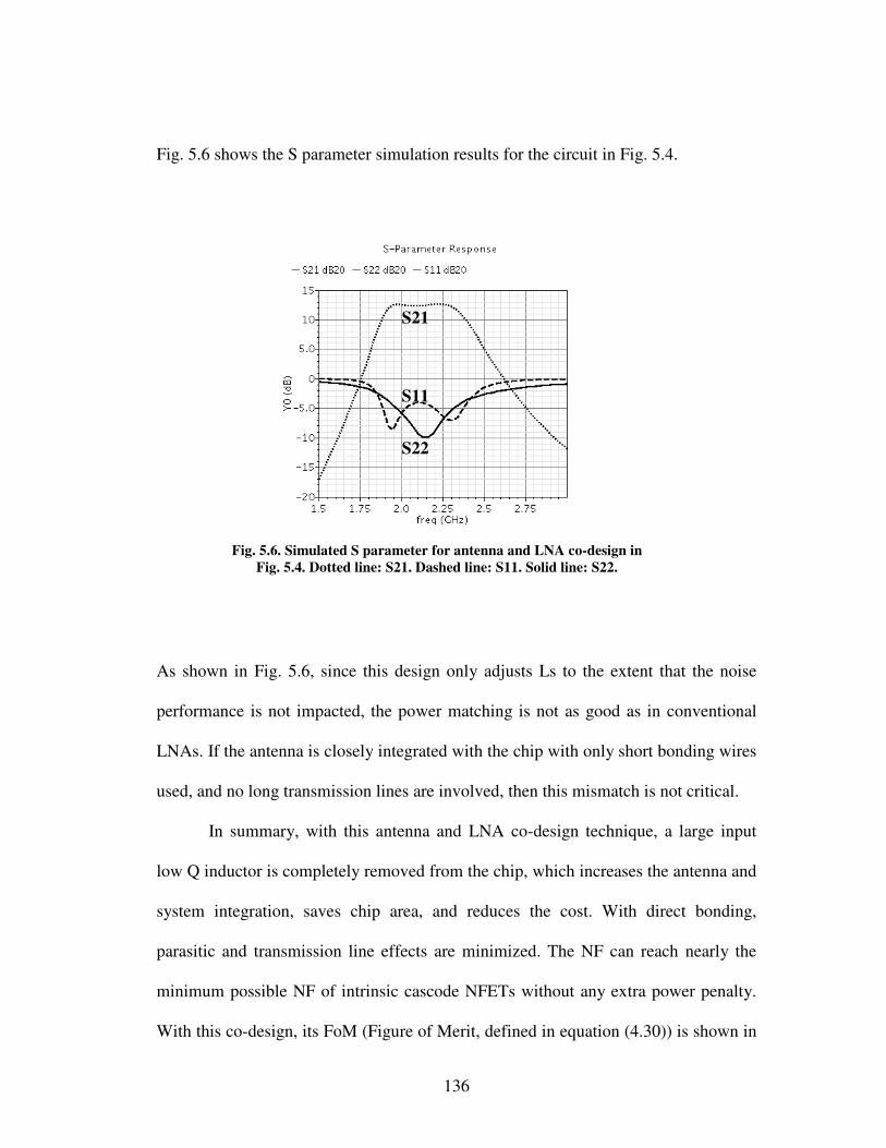
136
Fig. 5.6 shows the S parameter simulation results for the circuit in Fig. 5.4.
As shown in Fig. 5.6, since this design only adjusts Ls to the extent that the noise
performance is not impacted, the power matching is not as good as in conventional
LNAs. If the antenna is closely integrated with the chip with only short bonding wires
used, and no long transmission lines are involved, then this mismatch is not critical.
In summary, with this antenna and LNA co-design technique, a large input
low Q inductor is completely removed from the chip, which increases the antenna and
system integration, saves chip area, and reduces the cost. With direct bonding,
parasitic and transmission line effects are minimized. The NF can reach nearly the
minimum possible NF of intrinsic cascode NFETs without any extra power penalty.
With this co-design, its FoM (Figure of Merit, defined in equation (4.30)) is shown in
Fig. 5.6. Simulated S parameter for antenna and LNA co-design in
Fig. 5.4. Dotted line: S21. Dashed line: S11. Solid line: S22.
S21
S11
S22

137
Fig. 5.7 and it is compared with other works. As can be seen from Fig. 5.7, this co-
design technique largely helps to improve the FoM of the LNA.
5.4 Conclusion
This chapter has introduced a novel antenna and LNA co-design technique.
The use of a high Q factor antenna directly as the input matching network greatly
reduces the loss of on-chip inductors. This design has the advantages of increased
system integrity, a lower noise figure, and higher gain. In addition, this design is
robust to process variations due to its low noise sensitivity factor Rn. This co-design
technique largely increases the design integration level and reduces the development
cycle by considering the antenna performance at the earliest circuit design stage. It
has very good potential in commercial wireless communication radio.
Fig. 5.7 FoM (FoM2 = (Gain • f) / (F – 1) / Pdc) of LNAs. References in this figure
can be found in Table. 1.2.

138
Chapter 6 Low Power Receiver for Smart Dust
Wireless Sensor Networks
Chapters 3, 4, and 5 have devised novel solutions for the low form factor
antenna, the low power Low Noise Amplifiers (LNA), and their co-design for a Smart
Dust Wireless Sensor Network (SDWSN). The antenna and LNA are the first two
blocks in a Direct Demodulation Receiver (DDR) proposed in chapter 2. To complete
the full low power receiver design, this chapter applies various low power techniques
in designing the remaining blocks in a DDR, which includes an auxiliary amplifier, a
demodulation circuit, and a one channel Analog-Digital Converter (ADC). Highlights
of this work are:
1. Numerical and analytical behavioral models are derived for the
demodulator, which greatly assist the design of the demodulator and
the receiver.
2. While the low cost 0.13µm standard digital CMOS technology used
in this work does not provide high quality factor on-chip inductors,
this work still successfully designs a very low power receiver that
reduces the power consumption over the state of the art by a factor
of 9. With a 1.2V power supply, this receiver has a minimum

139
detectable signal of -58dBm, a data rate of 10kbps-2Mbps, a chip
area of 1.1mm2, and power consumption of only 2.85mW including
all biasing circuitries.
3. This receiver is fully integrated on-chip and completely removes all
off-chip components, which largely increases the level of
integration and reduces fabrication cost.
4. In addition, a full transceiver switch power control is designed and
simulated. By cutting off the transmitter’s power when the receiver
is on, it removes concern about transmitter interference and re-
radiation during receiving.
This chapter is organized as follows: Section 6.1 reviews the low power
analog/RF circuit design techniques that are applied in this work. Section 6.2 derives
the behavioral model and conversion gain for the demodulator, and also discusses
design concerns. Section 6.3 introduces the design of a low power auxiliary amplifier,
which applies current reusing and multiple stage cascading low power design
techniques. Section 6.4 presents the one channel ADC design. Section 6.5 illustrates
the SDWSN receiver layout and associated measurements. Section 6.6 discusses the
low power SDWSN transceiver design. Section 6.7 concludes this chapter.
6.1 Introduction
Several low power integrated circuit design techniques have been applied to
the ultra low power receiver in this work. The techniques are reviewed in this section.
In addition, continuous technology scaling also helps to reduce the power
consumption of analog circuits.

140
Low Rail-to-Rail Voltage
Power dissipation is the total DC current multiplied by the rail-to-rail voltage
(i.e., Vdd). Total power consumption is lower for smaller Vdds with the same DC
current. However, having low Vdd has several drawbacks: 1) Input and output swings
are limited. In particular, since the digital blocks work at the standard rail-to-rail
voltage (1.2V, in IBM 0.13µm technology), level shifters or buffers are required to
drive digital circuits at the analog-digital interface. 2) Having low Vdd also limits
circuit topology selection. For example, the typical threshold voltage for NMOS and
PMOS is around 0.3V to 0.4V. If the rail-to-rail voltage is reduced to 0.5V, then it
becomes difficult to stack transistors. Transistors stacked under low Vdd tend to work
in the subthreshold region, where the speed is poor. For this reason, this work does
not push the Vdd limit, but only demonstrates an ultra low power LNA biased at Vdd
= 1.2V and 1.0V.10
Current Reusing
Another way to save power is to stack as many functional blocks or transistors
as possible, so the biasing current of these blocks or transistors is reused. For
example, an inverter amplifier is formed by stacking a PMOS on top of a NMOS
transistor (Fig. 6.1). Both devices share the same biasing current ID, while they each
provide small signal gains of gmpro1 // ro2 and gmnro1 // ro2, respectively. gmp and gmn are
the transconductances of PMOS and NMOS devices. ro1 and ro2 are the output
resistances for NMOS and PMOS. The total gain is thus (gmp + gmn)ro1 // ro2, while the
10 The details of the LNA design are discussed in chapter 4.

141
power consumption excluding the bias is the same as a common source amplifier.
Similar current reusing ideas can be employed in more complicated circuit blocks
[Karanicolas96][Molnar04]. The drawback is that there is decreased voltage
headroom and swing. In addition, the noise analysis becomes more complicated when
multiple functional blocks are stacked [Molnar04]. This work applies the current
reusing method in an auxiliary amplifier design, whose noise is less important than in
the first LNA stage.
Cascading Multiple Amplifying Stages
The use of cascading multiple amplifying stages provides higher gain while
consuming less power [Daly07]. The fundamental idea is straightforward: if each
stage has the same gain and consumes the same amount of power, then by cascading,
the gain increases exponentially and the power consumption increases linearly. Many
RF amplifiers and baseband amplifiers use this cascading technique to achieve the
Fig. 6.1 Inverter amplifier using current reusing technique for higher gain and
lower power consumption.
142
same gain with lower power consumption [Daly07][Yao07]. The same technique is
applied in the auxiliary amplifier design of this work.
High Impedance Interface
From chapter 4, a high impedance interface saves power in the load and
provides high voltage gain. The technique is repeatedly used in this work. The
drawback is that usually this does not satisfy the conventional power matching
requirement. Therefore, if power matching is important, a high impedance interface
cannot be applied.
Subthreshold Biasing
If speed and noise are not critical parameters, amplifiers can be biased in the
subthreshold region, where static power consumption is significantly lower than in
the saturation region. Amplifiers biased in the subthreshold region have started to
appear in the literature [Perumana05]. However, due to unity gain limitations, this
technique is not applicable to circuits working above a frequency of a few GHz.
6.2 Receiver Circuitry
The detailed design of the low power LNA has been discussed previously in
chapter 4. From a low power IC design point of view, the cascode LNA under
consideration applies the current reusing technique by stacking a common gate
amplifier on top of a common source amplifier.
This section discusses the design of the demodulator, auxiliary amplifier, and
a one channel ADC.

143
6.2.1 Demodulator
Demodulator Design Goals
An envelope detector is chosen as the demodulator for the OOK receiver in
this work. Typical input and output signals of this demodulator are shown in Fig. 6.2.
The input of the demodulator comes from a preceding stage, which is a modulated
signal with DC offset. Its high frequency component and low frequency component
represent bit-1 and bit-0 in OOK modulation.
The output has voltage levels V1 and V2, where V1 > V2. After being rectified by the
demodulator, the high frequency input component becomes V1 with ripple Vout,RF,pp at
output. When the high frequency component is absent in the input, the envelope
detector discharges and reaches a level of V2. The output is nearly a square wave.
For the low power OOK DDR system in this work, the envelope detector
design goals include, but are not limited to:
Demodulator (envelope detector)
in out Vout,pp
Vout,RF,pp
ARF
TBB
TRF
V1
V2
Fig. 6.2 Demodulations of envelope detector in a direct demodulation receiver (DDR).

144
1. The output signal Vout,pp (peak-to-peak voltage) must be large enough to be
converted to a digital signal by the ADC.
2. The output ripple voltage Vout,RFpp should be small, and should not affect ADC’s
decision making.
3. Load capacitor charging and discharging time should be much less than the
baseband signal period TBB, so that the rising time and the falling time of the
output signal are negligible.
4. The envelope detector should provide high conversion gain Aconv, defined as
Aconv=Vout,pp / 2ARF.11 Definitions for Vout,pp and ARF are shown in Fig. 6.2.
5. We seek to maximize the gain (Aconv) to power consumption (Pdiss) ratio: Aconv /
Pdiss.
This work uses a diode-connected MOSFET driving a resistor and capacitor
parallel load as the envelope detector (Fig. 6.3). The diode-connected M1 rectifies the
input signal. The RC load filters the ripple.
11
As in mixers, the input and output signals of the envelope detector are at different frequencies. The transfer function of the peak detector is the ratio of the output signal voltage (at baseband) to the RF input signal amplitude, which is the conversion gain of the envelope detector.

145
RC Effect on Output Ripple and Baseband Signal
Intuitively, the bandwidth of this circuit is determined by the pole 1 / RC. This
pole needs to be much lower than the RF frequency so that all high frequency
components are filtered out. The pole also needs to be much higher than the baseband
frequency, so that all baseband signals have no attenuation.
We first study the RC effect on the output voltage ripple, by assuming the
input signal is:
( ) )()2
()(sin)( ,
0
tuVT
nTtunTtutAtV DCin
n
BBBBBBRFRFin +
−−−−= ∑
∞
=
ω , (6.1)
where Vin,DC is the DC offset coming from a previous amplifier stage. ARF is the
amplitude of the RF carrier, and ωRF = 2πfRF is the angular RF frequency. u(t) is a
step function. The term in the bracket is a square wave with period TBB, which
represents a simplified baseband signal with data rate of 1 / TBB. If M1 works as an
ideal diode, then:
−+=
RC
tAVtV RFDCinout exp)( , . (6.2)
Fig. 6.3 Schematic of diode-connected NMOS envelope detector.

146
The ripple voltage at the output is
RC
TA
RC
TA
RCAV RF
RFRF
RFRFRFppout ≈
−−
−= exp
0exp, . (6.3)
To minimize the RF ripple at the output, we need:
1, <<≈RC
TAV RF
RFRFppout . (6.4)
Fig. 6.4 shows the output ripple voltage being reduced by a larger RC product. In Fig.
6.4, R = 11.15 kΩ when sweeping C, and C = 1.57pF when sweeping R. Table. 6.1
lists other circuit parameters. If R is fixed, then the DC current and transistor biasing
do not vary with the RC product. A larger C provides a better AC shunt to ground,
and reduces the ripple. However, by varying R and fixing C, the DC current and
transistor biasing change with R and the output ripple does not decrease exponentially
with RC.
Table. 6.1. Simulation parameters used in Fig. 6.4.
ARF 50 mV
Vin,DC 600 mV
fRF 2.2 GHz
fBB 1 MHz
W/L mm µµ 12.020
Fig. 6.4 Envelope detector output voltage ripple as a function of R and C.
R C

147
To capture the slope of the baseband signal, TBB / RC >> 1 must be satisfied.
For example, if we want the output voltage to be within 1% its final value within TBB /
20, then TBB / RC ≈ 92. If TBB / RC ≈ 10, then the output voltage is within 10% of its
final value within TBB / 4.412.
For the above reasons, RC must meet the criteria TRF << RC << TBB. In low
power design, to maintain a small average current in M1 and a high output voltage
level, we should choose a larger R and a smaller C as long as TRF << RC << TBB is
satisfied.
Envelope Detector Behavioral Model and Conversion Gain
The envelope detector conversion gain is defined as the ratio of the output
baseband signal amplitude to the amplitude of the input high frequency signal. By
solving the envelope detector Kirchhoff’s current Law (KCL) or Kirchhoff’s voltage
Law (KVL) equations, we can derive the behaviorial model of the envelope detector
and the conversion gain as follows.
For minimum current consumption in the low power circuit, M1 operates in
the subthreshold region. Its drain current is [Gray01]:
−=
−−
T
ds
T
thgs
V
V
nV
VV
td eeL
WII
11
11 . (6.5)
W and L are the device width and length, respectively. tI is a constant that depends
on the process; TV is the thermal voltage; n is the subthreshold slope factor
12 As a side note, if the baseband signal is not a square wave, such as sine wave or triangular
wave, then the RC constant could be larger than the one picked for the square wave, as long as the slope of the RC attenuation is sharper than the slope of baseband signal.

148
[Gray01]13 . If we plot logID against VGS, logID approximately increases linearly with
VGS in weak inversion region. n is the factor that describes the slope of this variation.
Typically, n is a number between 1.1 to 1.5 [Taur98]. Vgs1 is the gate source voltage;
Vds1 is the drain source voltage of M1. Normally, Vds1 >> VT = 0.026V. Therefore, Id1
is simplified to
T
thgs
nV
VV
td eL
WII
−
≈
1
1 . (6.6)
If M1 is diode-connected, Vds1 = Vgs1. Then (6.5) becomes
−=
−−
T
ds
T
thds
V
V
nV
VV
constd eeII
11
11 . (6.7)
The I-V curves for a diode-connected transistor based on Cadence simulation
and (6.7) are shown in Fig. 6.5. W / L = 20µm / 0.12µm for M1. Its threshold voltage
13 In [Taur98], this is called the body effect coefficient.
Fig. 6.5 I-V curve of diode-connected NFET in subthreshold region.
Triangles: Analytical model according to Eq.(6.7).
Red solid line: Simulation results from Cadence.
Left: Linear coordinates. Right: Log coordinates.

149
Vth is 426.9mV. In the analytical model, we use n = 1.5V, It = 0.7µA. The subthreshold
model (6.7) matches the Cadence simulation very well.
The envelope detector can then be simplified by replacing the excitation and
M1 with an equivalent current source )(tI eq (Fig. 6.3, Fig. 6.6), which is a function of
input and output voltage. From (6.6) and (6.7),
−−+==
T
outDCthACinDCin
constdoutineqnV
tVVtVVItItVVI
)()(exp)(),,(
,,,
1 . (6.8)
)()( ,,, tVVtVV outDCthACinDCin −−+ is the gate source voltage vgs1(t) of M1. Vin,DC +
Vin,AC(t) is the input signal at gate, Vout(t) is the output signal at source, amd Vth,DC is
the threshold voltage. The expression of Vin,AC(t) is shown in equation (6.11).
Fig. 6.6 shows the equivalent circuit of the envelope detector. According to
KCL,
dt
tdVC
R
tVtI outout
eq
)()()( +=
. (6.9)
Therefore, the problem is defined as:
Fig. 6.6 Equivalent circuit of a peak detector.

150
0)(
exp),,(,,, =−−
−−+=
R
V
dt
dVC
nV
VVtVVI
dt
dVVtf outout
T
outDCthACinDCin
constout
out
(6.10)
( )
−−−−= ∑
∞
=0
, )2
()(sin)(n
BB
BBBBRFRFACin
TnTtunTtutAtV ω . (6.11)
The ordinary differential equation (6.10) is solved in MATLAB, and the
results are shown in Fig. 6.7. In this calculation, fRF = 2.2GHz, fBB = 1MHz, R =
46.89kΩ, C = 1.57pF, and W / L = 20µm / 0.12µm. Results in Fig. 6.7 are similar to
the Cadence simulation results, which verify the accuracy of this behavioral model.
However, numerically solving the ordinary differential equation (ODE) does not
provide significant design insight concerning the gain of the envelope detector. To
explicitly show the conversion gain, we next provide an analytical model using a
similar method given in [Meyer95].
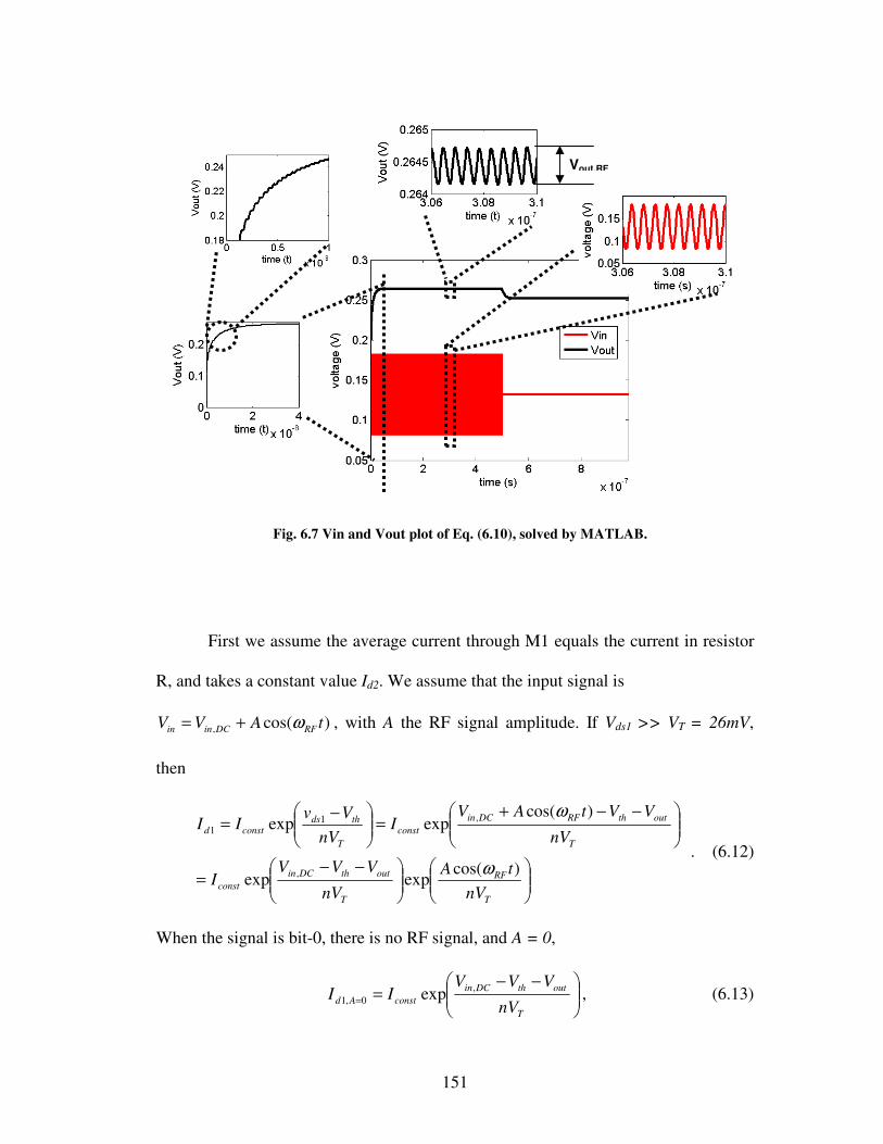
151
First we assume the average current through M1 equals the current in resistor
R, and takes a constant value Id2. We assume that the input signal is
)cos(, tAVV RFDCinin ω+= , with A the RF signal amplitude. If Vds1 >> VT = 26mV,
then
−−=
−−+=
−=
T
RF
T
outthDCin
const
T
outthRFDCin
const
T
thdsconstd
nV
tA
nV
VVVI
nV
VVtAVI
nV
VvII
)cos(expexp
)cos(expexp
,
,11
ω
ω
. (6.12)
When the signal is bit-0, there is no RF signal, and A = 0,
−−==
T
outthDCin
constAdnV
VVVII
,
0,1 exp , (6.13)
Fig. 6.7 Vin and Vout plot of Eq. (6.10), solved by MATLAB.
Vout,RF

152
min,
0,1
, ln out
const
Ad
TthDCinout VI
InVVVV =
−−= =
. (6.14)
When bit-1 is present, 0≠A , and
[ ]...)2cos()(2)cos()(2)(exp
)cos(expexp
210
,
,
0,1
+++
−−=
−−=≠
tbItbIbInV
VVVI
nV
tA
nV
VVVII
RFRF
T
outthDCin
const
T
RF
T
outthDCin
constAd
ωω
ω
, 6.15)
where )(bI n are modified Bessel functions of order n and TnVAb = [Meyer95].
The average current in M1 is:
2
,
0
,
,0,1
2exp
)(exp
d
b
T
outthDCin
const
T
outthDCin
constavgAd
Ib
e
nV
VVVI
bInV
VVVII
=
−−≈
−−=≠
π
(6.16)
max,
0
2,
)(ln out
const
dTthDCinout V
bII
InVVVV =
−−=⇒ , (6.17)
where
b
ebI
b
π2)(0 ≈ for b>1. (6.18)
The peak to peak output voltage is:
=−= =
2
0,10
min,max,,
)(ln
d
Ad
ToutoutppoutI
IbInVVVV . (6.19)
If we assume 20,1 dAd II == ,
( )
==
T
T
TTppout
nV
A
nV
A
nVbInVV
π2
exp
ln)(ln 0, . (6.20)

153
Therefore, outV and the conversion gain are both functions of n, VT, and A. The
output voltage vs. input voltage is plotted in Fig. 6.8 (a). The conversion gain (Aconv =
Vout,pp / 2A)is plotted in Fig. 6.8 (b). The output voltage amplitude is less than zero
when Vin,RF is less than 30mV. This is due to the limitation of the analytical model.
Nevertheless, the output error calculated using (6.20) is held within 12% if Vin,rf is
less than 100mV. From this calculation, the output of the auxiliary amplifier should
be at least around 50mV to satisfy design goal 1 in the beginning of this section.
Fig. 6.9 shows transient simulation results. It is worth noting that Vout reaches
its steady point very quickly within TBB, because BBRF TRCT <<<< . However, the
output still has small amount of ripple. This ripple must be suppressed to avoid
(a) (b)
Fig. 6.8 Cadence simulation and analytical model of a diode-connected envelope detector.
(a) Output voltage of the envelope detector and (b) conversion gain of the envelope detector.

154
possible error, because the next stage is a comparator with large gain and high
sensitivity.
One way to reduce this ripple is to increase C. Alternatively, another low pass
filter (R2, C2, Fig. 6.10) can be cascaded to the output of the envelope detector. The
Fig. 6.10 Envelope detector with ripple removing low pass filter.
Fig. 6.9 Simulated envelope detector performance without ripple remover.

155
demodulated signals with R2 and C2 are shown in Fig. 6.11. The ripple is almost
completely removed with the help of R2 and C2. The price paid here is the narrower
bandwidth due to the extra pole induced by R2C2.
6.2.2 Auxiliary Amplifier
The gain of a one stage LNA is not enough to drive the demodulator circuit.
Therefore, an auxiliary amplifier is necessary to provide an appropriate interface.
This work cascades 3 feedback amplifiers as the auxiliary gain stage, as shown in Fig.
6.12.
Fig. 6.11 Simulated envelope detector performance with ripple remover.

156
Component values are listed in Table. 6.2.
Table 6.2 Component values used in Fig. 6.12. W/L in µm/µm
W1/L1 W2/L2 W3/L3 W4/L4 W5/L5 W6/L6 R2 R3 R4
6/0.14 1.8/0.12 18/0.12 6/0.12 24/0.12 7.98/0.12 5.3kΩ 5.3kΩ 5.3kΩ
This design uses two of the low power circuit design techniques in section 6.1:
multiple amplifying stages cascading and current reusing. This amplifier can be
viewed as a PMOS feedback amplifier stacked on top of a NMOS feedback amplifier,
as shown in Fig. 6.13.
Fig. 6.12 Schematic of the auxiliary amplifier.

157
The small signal circuit model of a single stage is drawn in Fig. 6.14.
Similar to Fig. 6.1, the PMOS and NMOS amplifying stages share the same
DC bias current while both contribute voltage gain. R2 provides self-biasing and acts
Fig. 6.14 Small signal model of one stage of the feedback amplifier.
Fig. 6.13 The current reusing technique employed in the feedback amplifier.

158
like a feedback resistance. It senses the output voltage and feeds a current at the gate
of the amplifier. The low input and output impedance due to feedback makes it easier
to cascade each stage. In addition, the feedback resistors help to keep this multi-stage
amplifier from oscillating.
The total power consumption of this 3 stage amplifier is 1.08mW. The power
consumption includes the power of the envelope detector as well, because the
envelope detector is directly coupled to this stage without an individual bias.
6.2.3 Comparator
The output of the envelope detector is normally a very weak analog signal that
has a “high” representing bit-1 and a “low” representing bit-0. The peak to peak
voltage of this signal ranges only from 1mV to a few mV. In order to be identified by
a digital signal processor, an analog to digital converter (ADC) is needed.
The requirements for the comparator in this SDWSN receiver chain include
(but are not limited to): 1. Low power, 2. High resolution. 3. Medium to high
bandwidth, 4. High output swing, and 5. The ability to drive a digital circuit, such as a
register.
Since there is only one channel in the system, we only need a one bit ADC. A
low power voltage comparator is a very good candidate.
Three main voltage comparators are widely used in applications such as ADC,
data transmission, switching power regulators, etc. These comparators are: 1. Open
loop op-amps [Allen02]. 2. Clock controlled positive-feedback track-and-latched

159
comparators [John97]. 3. Switch capacitor comparators [Baker05]. The main
characteristics of these three comparators are summarized in Table. 6.3.
Table 6.3 Comparator types and characteristics.
Open loop op-amp comparators
Positive-feedback track-and-latched comparators
Sample-data comparators
Typical topology
Differential input high gain amp + single ended high swing output
Pre-amp + track-and-latch + output
Track and hold input + decision stage
Noise Input offset: 2mV to 5mV
Kickback noise in transitions
Provides offset cancellation
Clock circuit No Yes Yes
Auto-zero No Yes Yes
Power Consumption
Low High High
We choose a simple two stage open loop op-amp comparator in our design
because it requires no compensation or complicated multi-phase clock, and consumes
less power than other comparator architectures when resolution and output swing are
of most interest. For open loop op-amp comparators, a specific gain is not important.
By using proper design, its propagation delay and slew rate will meet the requirement
of a baseband signal ranging from 1mV to 20mV at a frequency up to 1MHz with
current consumption as small as 20µA.
As is shown in Fig. 6.15, the DC output from the envelope detector generally
ranges from less than 0.1V to 0.4V.

160
If the envelope detector is directly coupled to the input of the comparator, its
DC level is low. Therefore, A PMOS pair is preferred as the input stage to allow a
low input common-mode voltage. An initial design (Fig. 6.16) shows that with only
7µW power consumption, this comparator can provides a total voltage gain of
226V/V.
Fig. 6.15 DC output voltage of envelope detector vs. DC input voltage.

161
The minimum detectable signal of this comparator is 1mV (peak to peak), and the
output swing is around 0.42V. The two poles induced by the amplifying and output
stages are several times larger than 1MHz. The slew rate is estimated to be around
25ns. Therefore, the comparator is not gain-bandwidth or slew rate limited for signals
up to 1MHz.
Considering the uncertainties in the input common mode level, for
prototyping purposes, the input is AC coupled at a known DC level provided by Vref.
In order to isolate the parasitic capacitances of the op-amp, an inverter buffer is
inserted between the output and the capacitor load. The buffer consumes 9.6µW. This
device only consumes 30% of a NMOS’s input stage power with similar resolution
and output swing. More inverter stages with gradually increasing size could be added
if higher driving capability and minimum delay is required. By tuning the biasing
condition of the output stage, the valid operating range of this comparator is
Fig. 6.16 Comparator schematic. Transistor sizes of this comparator are listed in Table 6.4.

162
extended. To reduce the mismatch, minimum lengths are not used for transistors in
the differential pair. Transistor sizes (W/L in µm/µm) used in this design are
summarized in Table. 6.4.
Table 6.4 Sizes of transistors in Fig. 6.16. W/L in µm/µm
W/L1,2 0.64/0.5
W/L3,4 0.64/5.82
W/L5 1.25/0.12
W/L51 1.25/0.12
W/L6 0.64/0.3
W/L7 2.4/0.12
W/L71 0.8/0.12
W/L8 0.93/0.32
W/L9 0.64/0.32
Due to probe station testing limits, we have to limit the total number of DC
biases or DC references used in the design. Therefore, in the prototype receiver, one
side of the input is directly coupled to the output of the envelope detector. The other
is biased manually to tune out the offset of the comparator. Comparators for battery
powered receivers may need DC offset cancellation circuits, which normally require a
two-phase clocking circuit with more complicated component parts and more power
consumption.
6.3 Layout and Experimental Results
Fig. 6.17 shows the layout of this receiver. This receiver only occupies an area
of 1.0mm × 1.1mm, including all bonding pads. Electromagnetic effects and

163
semiconductor manufacturing effects should both be considered in this layout, which
are discussed in detail as follows.
From an electromagnetic compatibility and signal integrity point of view, the
power rail and ground traces should be carefully arranged. For almost all integrated
circuits, on-chip power traces carry large current and should be kept wide and short to
reduce the DC IR (current multiplied by wire resistance) voltage drop. To find the
limitations on the width and length, we need to further discuss the high frequency
effect of these wide metal traces.
Fig. 6.17 Layout of full OOK receiver using 0.13µm technology.

164
Depending on packaging methods, on-chip power rails and ground traces and
the ground plane (or ground planes) form microstrip lines (or triplate lines)
[Cheng92]. For chips packaged in a normal way, a ground plane appears at the
bottom of the substrate after packaging, which coincides with the ground plane
defined on the printed circuit board (Fig. 6.18 (a)). In this way, an on-chip metal trace
and this ground plane form a microstrip line. For flip-chip packaging technology, the
chip is flipped over, facing the ground plane defined by the printed circuit board. Its
original ground plane now becomes the ceiling plane after packaging. The “ceiling” is
defined to have the same potential as the printed circuit board ground plane (Fig. 6.18
(b)). In this way, a metal strip on the die now is sandwiched between ground planes,
which forms a triplate line.

165
Since flip-chip technology was not available to university users, we only
discuss details of the microstrip line in this section. If we neglect the losses and the
fringe effects, the microstrip line in Fig. 6.18 (a) can be simplified to a parallel plate
transmission line, for which the unit length inductance L and unit length capacitance
C are [Cheng92]:
w
dL µ= (H/m), (6.21)
d
wC rεε 0= (F/m), (6.22)
where d is the distance between the metal strip and the ground plane, w is the metal
strip width, µ is the permeability constant (same as the permeability constant in air
Printed Circuit
Board
Ground
Plane
Packaged
Chip
Metal strip
(a)
Printed Circuit
Board
Ground
Plane
Flip-Packaged Chip
Metal strip
(b)
Chip bottom
Chip top
Chip top
Chip bottom
Fig. 6.18 Cross sectional plots of (a) a microstrip line formed in normal
packaging, and (b) a triplate line formed in flip-chip packaging.

166
(4π × 10-7 (H/m), since the semiconductor substrate is not a magnetic material), ε0 is
the permittivity constant in air (1/36π × 10-9 (F/m)), and εr is the dielectric constant of
the material between the metal strip and the ground plane. If there is a ground trace
right underneath the power trace, then a parallel plate transmission line is formed.
(6.21) and (6.22) thus provide even better estimation accuracy.
The dielectric constant εSiO2 for silicon dioxide is around 4. The dielectric
constant εSi for silicon substrate is around 11 to 12. For estimation purposes, we
assume εr is a weighted average of these two14:
ddd SiOSiOSiSir /)(22
εεε += , (6.23)
2SiOSi ddd += , (6.24)
where dSi is the substrate thickness, and dSiO2 is the distance between the bottom of the
metal strip and the silicon dioxide-substrate interface. To reduce the unwanted metal
layer-to-layer coupling capacitance, multiple silicon dioxide layer (These layers have
different thickness and dielectric constant.) are used between adjacent metal layers. A
more accurate effective dielectric constant should be determined with careful
considerations concerning the particular layers used by a selected process (For a same
technology, some metal layers may not be available to a particular fabrication. This
information is obtained from the foundry.).
According to (6.22), parasitic capacitance increases with the metal trace width
w, and decreases with the metal trace-to-substrate distance d. For power rails, having
larger rail-to-ground parasitic capacitance indeed helps to reduce high frequency
14 For a microstrip line, the effective dielectric constant at better accuracy can be found in
[Pozar05]. However, as this work explains, obtaining a closed form for the effective dielectric constant is not trivial for multi-layered dielectric-microstrip structures.
167
noise on the bias. As we can see from Fig. 4.22, a bypass capacitor is connected from
Vdd to ground to provide a path for high frequency noise, and to thus prevent the
high frequency noise contaminating the Vdd biasing. The rail-to-ground parasitic
capacitance induced by wide power rails appears parallel to this bypass capacitor.
Therefore, wide power traces not only help to reduce the capacitor size of that bypass
capacitor (which saves the chip area), but also provide the bypass capacitance along
the power rail in a distributed fashion.
Now we examine the effect of the induced parasitic inductance. If the supply
current ∆I varies within ∆t, then for a unit length inductor L, a voltage bounce of ∆V
is induced along the power trace, where
t
ILV
∆
∆≈∆ . (6.25)
To suppress this voltage bounce, L should be small. According to (6.21), the
metal trace width w should be larger, and the trace should be close to the ground
plane (i.e., using lower metal layers, such as metal 2 layer).
From the above analysis, for power and ground traces, wide metal strips
composed by lower metal layers should be used to increase the unit length capacitor
and reduce the unit length inductor of the microstrip lines at high frequencies.
However, lower metal layers are normally thin metal layers with smaller cross-
sectional area. Therefore the DC ohmic loss and high frequency ohmic loss (At high
frequency, the cross-sectional area is the skin depth multiplied by the perimeter
length of the metal cross section.) are both higher. To compensate for this, multiple
metal layers can be stacked together through vias to increase the cross-sectional area
at both DC and high frequencies.

168
From the above discussion, this work applies the following rules of thumb for
power and ground traces:
1. We stack as many lower metal layers as possible (metal 2 to metal 6
layers) to construct Vdd paths. Metal layers are electrically connected using
vias. The metal1 layer is reserved for ground traces.
2. We manually rout the Vdd path to make its overall length as short as
possible to reduce the ohmic loss at both DC and high frequencies.
3. We use wide Vdd and ground paths to the extent that design rules are not
violated, to increase the distributed Vdd-to-ground bypass capacitance, and to
reduce the unwanted unit length inductance. Whenever applicable, ground
paths are positioned right underneath power traces.
4. The maximum width of power and ground traces should not violate design
rules.
The PDK for the 0.13µm CMOS used in this work provides some parasitic
extractions. To investigate the rigorous RF effects of power and ground traces, RF
simulations need to be conducted on critical nets. The knowledge of process profile
details and exact layout geometry must be obtained to perform an accurate simulation
and analysis. Certain critical data (such as substrate thickness and conductivity) are
usually not disclosed to university users. A study of power and ground trace RF
effects with a high level of accuracy is expected to be developed in the future.
From a semiconductor fabrication point of view, candidate layouts should
avoid “antenna” rule violations. During the plasma etching process, charges
accumulate on metal lines. When the gate of a small transistor is connected to metal

169
lines that have a large accumulated charge, the gate dioxide may break down. This is
called the “antenna” effect. To prevent such a result, there are two common layout
techniques used. One is to use other metal layers. For example, if metal 1 has an
antenna effect, then we should reduce the area of metal 1 being used, and “jump” to
another metal layer, such as metal 2, through vias to complete the routing. Another
method is to connect tie-downs to the gate, such as p+/nwell or n+/substrate devices.
These tie-downs are reverse-biased diodes that provide a current path from gate to
substrate for dissipating the built up charge during fabrication.
In addition, to meet the metal density rule, wide metal traces used in power
rails, ground rails, and inductors are often striped or slotted. By striping, a wide metal
trace is replaced by several minimum width metal traces in parallel. The metal to
metal spacing should satisfy process design rules (Fig. 6.19 (a)). With slotting,
interleaved slots are introduced to a wide metal trace, so that the metal density is
more uniformly distributed in all directions (Fig.6.19 (b)). In addition, the metal side
wall to side wall coupling capacitance is less in slotted metal lines than in striped
metal lines. Since currents are more concentrated at the edge of metal lines at high
frequencies due to the skin effect, for a given metal width, slotted or striped metal
lines do not reduce the number of edges over which the current can flow. In other
words, slotting and striping do not bring more ohmic loss at high frequencies than
simple wide metal traces. However, it is very demanding to manually layout metal
traces with stripes and slots without violating any design rules, especially when multi-
layer metal traces are desired. Normally, complex layouts like these are processed by

170
Electronic Design Automation (EDA) software, such as Peakview [Lorentz]. In the
0.13µm CMOS technology applied in this work, no slotting or striping is provided.
(a)
(b)
metal (in gray)
Openings (in white) on
the metal trace (striped)
Openings (in white) on
the metal trace (slotted) metal (in gray)
Fig. 6.19 (a) A wide metal strip being striped. (b) A wide metal strip being slotted.

171
The prototype receiver test bench is shown in Fig. 6.20.
Fig. 6.21 shows the die microphoto of the receiver.
1.1 mm
GN
D
GN
D
TX
GN
D
OU
T
VL
NA
VD
D
VA
MP
VC
MP
VR
EF
GND
GND
IN
GND
1.0
mm
Fig. 6.21 Microphoto of the receiver.
Fig. 6.20 Receiver test bench.

172
Fig. 6.22 shows the test results. With 2.85mW measured total power
consumption, the receiver can correctly demodulate an input signal as small as
-58dBm.
Table 6.5 summarizes the receiver performance.
Output 1.138 Vpp 10 kbps
Input 812 µVpp ( = -58dBm) 2.2 GHz
Fig. 6.22 Transient testing results of receiver.

173
Table. 6.5 Summary of receiver performance.
While the 0.13µm standard digital CMOS technology used in this work does
not provide high quality factor on-chip inductors, this work still successfully designs
a very low power receiver which reduces the power consumption by a factor of 9
comparing to the state of the arts.
6.4 Transceiver Design and Results
A full 2.2 GHz transceiver with switch control of the power supply was
designed and fabricated. Fig. 6.23 (a) shows the schematic of this system, and Fig.
6.23 (b) shows a simplified diagram. The transmitter was designed by Yiming Zhai
[Zhai09] and Thomas Salter [Salter09]. For completeness, the schematic of the
transmitter is shown in Fig. 6.24. Details of the transmitter analysis can be found in
[Zhai09; Salter09].
Features [Morici09] [Retz09] [Hafez07] This work
Technology 90nm 0.18µm RFCMOS
0.13µm 0.13µm Digital CMOS
Availability of high Q inductor in this technology (determines the cost)
None Yes None None
External component None None None None Supply Voltage (V) 1.2 1.8~3.6 1.2 1.2
12.6~25.2 (receiver only)
Power Consumption (mW)
3.6
30.24~60.48 (full receiver)
7.2 2.85
Data Rate (kbps) -- -- -- 10 ~ 2000 Carrier Frequency (GHz) 2.45 2.4 2.45 2.2 Die Area (mm2) 0.12 5.9 -- 1.1 Sensitivity (dBm) -- -96 -97 (simulated) -55

174
(a)
(b)
Fig. 6.23 Full OOK transceiver system schematic.

175
The full transceiver uses a 2-bit baseband control signal CtrTx CtrRx and two
sets of switches to direct the signal path. One is the RF switch (Fig. 6.25), and the
other is the power rail low frequency control switch (a simple transmission gate,
whose plot can be found in standard text books).
From Fig. 6.25, if there is no significant DC offset at Tx or Rx, ST and SR
should set to 0V. Otherwise, ST should be equal to Tx’s DC offset, and SR should be
set equal to Rx’s DC offset. VctrR = 1.2V and VctrT = 0V when the receiver is on.
VtrrR = 0V and VctrT = 1.2V when the transmitter is on. Component parameters
(W/L in µm/µm) used in the RF switch are listed in Table 6.6.
Fig. 6.24 Transmitter schematic of OOK system, from [Zha09] and [Salter 09]

176
Table 6.6 Component parameters in Fig. 6.25. (W/L in µm/µm)
M1 M2 M3 M4 R C
240/0.12 240/0.12 240/0.12 240/0.12 11.3kΩ 30pF
Transceiver operation statuses versus CtrTx and CtrRx are summarized in
Table 6.7.
Table 6.7 Transceiver operation status vs. control bits.
CtrTx CtrRx 10 (Fig. 24(a))
01 (Fig. 25(a))
00 11
Tx_Vdd Vdd ground ground
Rx_Vdd ground Vdd ground
Antenna RF path for receiver
highly isolated
on
Antenna RF path for transmitter
on highly isolated
Receiver off On idle
transmitter on off idle
Not Allowed
In addition to saving power, the transmitter power is cut off when the receiver
is on, and this removes the concern of transmitter interference and re-radiation during
Fig. 6.25 RF switch schematic for the OOK transceiver.

177
receiving. The simulated results for transmitting and receiving are shown in Fig. 6.26
(b) and Fig. 6.27 (b), respectively.
(a) (b)
Antenna (mV)
Rx,input (mV)
Tx,output (µV)
Fig. 6.27 Simulated results for full transceiver system with receiver on.
(a) (b)
Fig. 6.26 Simulated results for full transceiver system with transmitter on.
Rx,input(mV)
Tx,output(mV)
Antenna(mV)
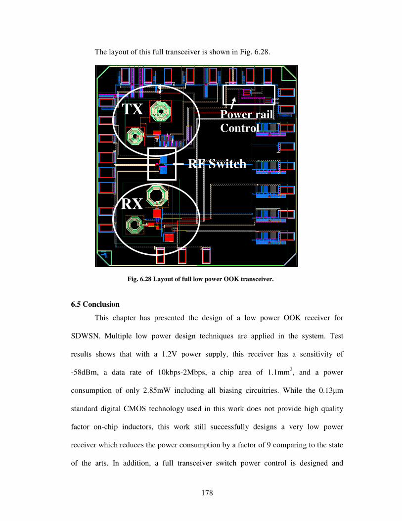
178
The layout of this full transceiver is shown in Fig. 6.28.
6.5 Conclusion
This chapter has presented the design of a low power OOK receiver for
SDWSN. Multiple low power design techniques are applied in the system. Test
results shows that with a 1.2V power supply, this receiver has a sensitivity of
-58dBm, a data rate of 10kbps-2Mbps, a chip area of 1.1mm2, and a power
consumption of only 2.85mW including all biasing circuitries. While the 0.13µm
standard digital CMOS technology used in this work does not provide high quality
factor on-chip inductors, this work still successfully designs a very low power
receiver which reduces the power consumption by a factor of 9 comparing to the state
of the arts. In addition, a full transceiver switch power control is designed and
RF Switch
RX
TX Power rail
Control
Switch
Fig. 6.28 Layout of full low power OOK transceiver.

179
simulated. By cutting off the transmitter’s power when the receiver is on, it removes
the concern of transmitter’s interference and re-radiating during receiving.

180
Chapter 7 Summary and Future Work
7.1 Research Summary
As opposed to traditional handheld wireless devices or conventional radios in
wireless sensor networks, Smart Dust Wireless Sensor Networks (SDWSN) have
aggressive low-form-factor, low-power, and low-cost requirements on their
communication nodes. This research provides innovative solutions to cope with these
challenges. In particular, it successfully designs a new electrically small antenna
whose volume (including ground plane) is only 7% of other state-of-the-art small
antennas, while its efficiency (48.53%) and gain (-1.38dBi) are comparable to
antennas of much larger dimensions. This work also proposes a novel low power Low
Noise Amplifier (LNA) design method, and the designed LNA has a figure of merit
that is twice as high as the best found in the literature evaluated by identical criteria.
In addition, this work devises an antenna and LNA co-design method, which greatly
increases the level of design integration, reduces the development cycle, and achieves
a noise figure of only 1.5dB with 2mW power consumption. Finally, this work
designs a low power (2.85mW) OOK receiver that is fully integrated using a standard
0.13µm CMOS process with a die area of only 1.1 mm2. It removes all receiver off-
chip components that are frequently reported in the literature.

181
This dissertation has reviewed the design challenges involved and proposes a
simple receiver structure that is suitable for low power, low data rate SDWSN
applications. The invention of a low profile, scalable, highly efficient F-Inverted
Compact Antenna (FICA) has been presented herein. The antenna’s performance is
verified through simulations and measurements in free-space and inside an anechoic
chamber. Its validity in SDWSN is measured by antennas mounted on SDWSN
nodes. This work also presents a complete parametric analysis of this FICA and
proposes a physics based circuit model. This model is verified through S11
measurements. This FICA also shows excellent performance when it is scaled to
other frequencies.
Next, a systematic LNA design and optimization method was proposed in this
work. We emphasize the advantage of voltage gain design, and discuss the trade offs
and active device sizing and biasing in detail. In particular, loss of the spiral inductors
in the input matching network is compensated by a negative input impedance induced
by high output load coupling. This helps to increase the quality factor of the input
network and the overall voltage gain of the LNA. A 2.2GHz LNA following these
unique design strategies shows a high figure of merit, when compared to others found
in the literature.
Coupling the antenna circuit model with the LNA design and optimization
methodology, this work additionally proposes a novel antenna and LNA co-design
technique, in which the high quality factor (Q) inductor of the FICA serves also as
part of the LNA input matching network. This not only removes the need for large-
area spiral inductors in the input network, but also increases the Q of the input

182
network. By properly selecting the FICA tapping point, an input matching circuit
primarily composed of the high Q antenna provides a very low noise figure (1.5dB).
In addition, this design is very robust to noise, so it can work properly across process
variations.
Lastly, a full Direct Demodulation Receiver for SDWSN is introduced in this
work. The behavioral model of the demodulation block is characterized. Alternative
low power techniques are reviewed and applied in different receiver circuit blocks.
This receiver has a sensitivity of -58dBm and power consumption of 2.85mW. This
receiver has completely removed all off-chip components, and occupies only a
1.1mm2 die area. A full transceiver with switch power control is designed and
simulated in this work. In addition, the transmitter’s power is cut off when the
receiver is on and this removes the concern for transmitter interference and re-
radiation during receiving.
7.2 Future Work
7.2.1 Radio Units for SDWSN at Tens of GHz
The size of the radio unit for this current work is on the order of 1 to 2 cubic
centimeters. The antenna is the most bulky part of the device. To further reduce the
volume of the radio, we need to investigate the viability of radios and antennas at tens
of GHz. As an example, at 20GHz, FICA size is a few mm, but more transmitting
power is needed to maintain the same communication distance for the reasons
discussed in chapter 2. Therefore, novel antennas with higher gain are needed for
SDWSN working at 20GHz or higher bands.

183
7.2.2 System Integration
This work has demonstrated the benefits of a highly integrated antenna and
LNA co-design. Some prototype radios with FICAs and off the shelf circuits, sensors,
and batteries were assembled and made fully functional. However, a compact fully
integrated system including the circuits and antennas in this work which also uses
more efficient batteries and sensors is yet to be completed.
7.2.3 New SDWSN Radio with Advanced Technology
This work applies 0.13µm standard digital CMOS technology. With advanced
technologies, higher Q spiral on-chip inductors help to increase the gain and reduce
the noise level of amplifiers. With the flip-chip packaging technique, less parasitic
elements are introduced into the circuit, and the radio can be designed for higher
frequencies.

184
Appendix A
To derive Equation (4.1), we use the following circuit (Fig. A.1)
The derivation of Equation (4.1) is as follows:
o
sgs
gs
Rsmgsm iRCj
Cjvgvg =
+=
ω
ω
/1
/1 (A.1)
gs
m
Rs
o
mCj
g
v
iG
ω+==⇒
1 . (A.2)
The output noise due to 2
,Rsnoi is:
2222
, 4 msmRsRsno GfRkTGvi ∆== . (A.3)
The output noise due to 2
,indnoi is:
dsoindindno gfkTii γ∆≡= 422
, . (A.4)
Fig. A.1 Small circuit model for an intrinsic transistor including drain
current noise.

185
The noise factor is :
( )2
22
22
,
2
,1
14
41
ms
gsdso
ms
dso
Rsno
totalno
gR
Cg
GfRkT
gfkT
v
vF
ωγγ ++=
∆
∆+== . (A.5)
If we define
dso
m
g
g≡α , (A.6)
then,
221 gss
msm
CRgRg
F ωα
γ
α
γ++≈ . (A.7)

186
Appendix B
Derivations for optimum noise impedance in chapter 5: To derive the optimum noise impedance, we use the following small signal circuit
(Fig. B.1):
Step1: Short the input and find the equivalent voltage noise source:
(1) 2
1,,shoni due to 1gR is:
2
1
2
1,, 1gRshon vai = , (B.1)
where
( )sggs
mRRCj
Ga++
=11
11
1
ω , (B.2)
11
1
1 ggs
mm
RCj
gG
ω+
−= . (B.3)
Fig. B.1 The small signal circuit model for the optimum noise impedance
derivation.

187
(2) 2
2,,shoni due to 2
1ngi is:
2
12
2
2,, ngshon iai = , (B.4)
where
( ) ( )
( )
1
112
11121211
2
1−
−
−−++
++
=mgdm
mgdgdgsgdmgdgs
gCjg
gCjCjCjCjgCjCjR
aω
ωωωωωω
,
(B.5)
1gs RRR += . (B.6)
(3) 2
3,,shoni due to 2
1ndi is:
2
13
2
3,, ndshon iai = , (B.7)
where
( )
1
2
11
11111
2
31
11
−
+
++
+++−= gs
gsgd
gsgdgdmgd
m
CjRCCj
RCjCjCjRgCj
ga ω
ω
ωωωω. (B.8)
(4) 2
4,,shoni due to 2
2ndi is:
2
24
2
4,, ndshon iai = , (B.9)
where
( )
+
++
+++−=
−1
2
11
11111
2
41
111 gs
gsgd
gsgdgdmgd
m
CjRCCj
RCjCjCjRgCj
ga ω
ω
ωωωω . (B.10)
(5) 2
5,,shoni due to 2gR is:

188
2
25
2
5,, Rgshon vai = (B.11)
where
( )( )
( )[ ]( )
22
11
1
22
11
222
2
11
1
22
11
22
5
11
1
1
1
1
ggd
gdgs
gd
gsm
gsm
ggsgd
gd
gdgs
gd
gsm
gsm
mgd
RCj
CCjR
Cj
Cjg
CjR
g
RCCj
Cj
CCjR
Cj
Cjg
CjR
g
gCj
a
ωω
ω
ω
ωω
ωω
ω
ω
ωω
++
++
+
++++
+
++
+
++−
=
(B.12)
Therefore,
+++++
+=
==
L
ngndndngRg
m
ggs
m
Tshon
eqn
R
KTiaiaiaiava
g
RCj
G
ive
412
25
2
24
2
13
2
12
2
11
1
11
2
,,22
ω , (B.13)
+++++
+==
L
ngndndngRg
m
ggs
eqnR
KTiaiaiaiava
g
RCjve
412
2
2
5
2
2
2
4
2
1
2
3
2
1
2
2
2
1
2
1
2
1
1122ω
,
(B.14)
KT
eR n
n4
2
= . (B.15)
Step 2: Open the input and find the equivalent current noise source.
(1) 2
1,,oponi due to 1gR is : 0.
2
1
2
1,, 1gRopon Vbi = , (B.16)
Where
01 =b . (B.17)

189
(2) 2
2,,oponi due to 2
1ngi is:
212
22,, ngopon ibi = , (B.18)
where
( )( ) ( )( )
1
112
11121211
2
−
−
−−+++=
mgdm
mgdgdgsgdmgdgs
gCjg
gCjCjCjCjgCjCjb
ω
ωωωωωω . (B.19)
(3) 2
3,,oponi due to 2
1ndi is:
2
13
2
3,, ndopon ibi = , (B.20)
where
1
2
11
11
2
11
11
23
−
−
+−−
+
−= m
gdgs
gdgs
gs
gdgs
gdm
m gCC
CCjCj
CC
Cggb ωω . (B.21)
(4) 2
4,,oponi due to 2
2ndi is:
2
24
2
4,, ndopon ibi = , (B.22)
where
34 1 bb −= . (B.23)
(5) 2
5,,shoni due to 2
2ngi is ignored, and not included in this calculation.
Therefore,
2
,2
22
oponeqn ibii == , (B.24)
222222
uncuceqn ieYiiii +=+== , (B.25)
( ) 2
ncnuncnn eYeieYei >=⋅+>=<⋅< , (B.26)

190
cc
L
ndndngRg
m
ggs
n
n
nn
c
jBG
R
KTibaibaibavba
g
RCj
e
b
e
eiY
+=
++++
+=
>⋅<=
412
244
2
133
2
122
2
111
1
11
2
2
2
ω , (B.27)
222
ncnu eYii −= , (B.28)
2222
ncnu eYii −= , (B.29)
KT
iG u
u4
2
= , (B.30)
KT
eR n
n4
2
= . (B.31)
According to [Lee03], the optimum source impedance and minimum noise figure are:
cc
n
uopt jBG
R
GY −+= 2 , (B.32)
+++= cc
n
u GGR
GRF
n
2
min 21 . (B.33)
Yopt and Fmin can be easily achieved once variables in the right hand side of (B.32) and
(B.33) are calculated following (B.1) to (B.31).

191
Bibliography
[Antennafactor1] ANT-916-CW-RCL data sheet, Available:
www.antennafactor.com. [Antennafactor2] ANT-916-CHP-T data sheet, Available: www.antennafactor.com. [Abedin03] M. F. Abedin and M. Ali, “Modifying the Ground Plane and its
Effect on Planar Inverted-F Antenns (PIFAs) for Mobile Phone Handsets,” IEEE Antennas and Wireless Propagation Letters, vol. 2, pp. 226-229, 2003.
[Abidi95] A. A. Abidi, “Direct-conversion radio transceivers for digital
communications,” IEEE J. Solid State Circuits, vol. 30, no.12, pp. 1399-1410, Dec. 1995.
[Abidi04] A. A. Abidi, “RF CMOS comes of age,” A. A. Abidi, IEEE J.
Solid State Circuits, vol. 39, no.5, pp. 549-561, Apr. 2004. [Allen02] P.E.Allen and D.R. Holberg, “CMOS Analog Circuit Design,”
Oxford University Press, Inc. 2002, ISBN 0-19511644-5. [Andreani01] P.Andreani, and H. Sjoland, “Noise optimization of an inductively
degenerated CMOS low noise amplifier,” IEEE Trans. Circuits
and Systems (II) Analog and Digital Signal Processing, vol. 48, no. 9. pp. 835- 841, Dep. 2001.
[Baker05] R.J. Baker, H.W. Li, and D.E. Boyce, “CMOS Circuit Design,
Layout, and Simulation,” Revised 2nd Edition, John Wiley & Sons,
Inc. ISBN-978-0-470-22941-5. [Balzano81-I] Q. Balzano, O. Garay, and K. Siwiak, “The Near Field of Dipole
Antennas, Part I: Theory”, IEEE Trans. on Vehicular Technology, vol.30, no.4, pp. 161-174, Nov. 1981.
[Balzano81-II] Q. Balzano, O. Garay, and K. Siwiak, “The Near Field of Dipole
Antennas, part II: Experimental Results,” IEEE Trans. on
Vehicular Technology, vol.30, no.4, pp. 175-181, Nov. 1981. [Bassen83] H. I. Bassen, “Electric Field Probes for Cellular Phone
Dosimetry,” Proceedings of the 19th Annual International
Conference of the IEEE Engineering in Medicine and Biology
Society, vol. 6, pp. 2492-2495, Oct. 30- Nov. 2, 1997.
192
[Bell04] J. M. Bell and M. F. Iskander, “A Low-Profile Archimedean Spiral Antenna Using an EBG Ground Plane,” IEEE Antenna and
Wireless Propagation Letters, vol. 3, pp. 223-226, 2004 [Bevilacqua04] A. Bevilacqua and A. M. Niknejad, “An ultrawideband CMOS
low-noise amplifier for 3.1-10.6-GHz wireless receivers,” IEEE J.
Solid State Circuits, vol. 39, no. 12, pp 2259 – 2268, Dec. 2002. [Boyle06] K. R. Boyle, L. P. Ligthart, “Radiating and Balanced Mode
Analysis of PIFA Antennas,” IEEE Trans. on Antennas and
Propagation, vol.54, no.1, pp. 231-237, 2006. [BSIM] http://www-device.eecs.berkeley.edu/~bsim3/bsim4.html. [Cadence] http://www.cadence.com. [CC1110] CC1110 Preliminary Datasheet (Rev. 1.01) SWRS033A, Chipcon
AS, 2006. [CC2430] CC2430 datasheet, Available:
http://focus.ti.com/lit/ds/swrs036f/swrs036f.pdf. [Chen05] H.-M. Chen, Y.-F. Lin, P.-S. Cheng, H.-H. Lin, C.T.P. Song, P.S.
Hall, “Parametric Study on the Characteristics of Planar Inverted-F Antenna,” IEE Proc. –Mocrow. Antennas Propag., vol. 152, no. 6, Dec, 2005.
[Choi03] P.Choi, H. C. Par, S. Kim, S. Par, I. Nam, T. W. Kim, S. Par, S.
Shin, M. S. Kim, K. Kang, Y. Ku H. Choi, S. M. Park, and K. Lee, “An experimental coin-sized radio for extremely low-power WPAN (IEEE 802.15.4) Application at 2.4 GHz,” IEEE J. Solid
State Circuits, vol. 38, no.12, pp. 2258 – 2268, Dec. 2003. [Choo05] H. Choo, R. L. Rogers, H. Ling, “Design of Electrically Small
Wire Antennas Using a Pareto Genetic Algorithm,” IEEE Trans.
on Antennas and Propagation, vol.53, no.3, pp. 1038-1046, March, 2005.
[Chu48] L. J. Chu, “Physical Limitations of Omnidirectional Antennas,” J.
Appl. Phys., Vol. 19, 1948. [Chuang03] H.-R. Chuang and L.-C. Kuo, “3-D FDTD design analysis of a 2.4
GHz polarization-diversity printed dipole-antenna with integrated balun and polarization-switching circuit for WLAN and wireless communication applications,” IEEE Trans. Microwave Theory
Tech., vol. 51, no. 2, pp. 374–381, Feb. 2003.

193
[Cook06] B.W. Cook, S. Lanzisera, and K. S. J. Pister, “SoC issues for RF
smart dust,” Proceedings of the IEEE, vol. 94, no. 6, pp. 1177 – 1196, Jun. 2006.
[Crossbow] www.xbow.com. [Daly07] D. C. Daly and A. P. Chandrakasan, “An energy-efficient OOK
transceiver for wireless sensor networks,” IEEE J. Solid State
Circuits, vol. 42, no. 5, pp. 1003- 1011, May 2007. [Darabi00] H. Darabi and A. A. Abidi, “A 4.5-mW 900-MHz CMOS receiver
for wireless paging,” IEEE J. Solid State Circuits, vol. 35, no. 8, pp 1085 – 1096, Aug. 2000.
[DeJean07] Gerald R. DeJean, Manos M. Tentzeris, “The Application of
Lumped Element Equivalent Circuits Approach to the Design of Single-Port Microstrip Antennas,” IEEE Trans. Antennas and
Propagation. vol. 55, no. 9, pp.2468-2472, Sep, 2007. [EKV95] C.Enz, F. Krummenacher, and E.Z. Vittoz, “An Analytical MOS
Transistor Model Valid in All Regions of Operation and Dedicated to Low-Voltage and Low-Current Application,” Analog Integrated
Circuit and Signal Processing, vol. 8, pp. 83-114, 1995. [Friis44] H.T. Friis, “Noise Figure of Radio Receivers,” Proc. IRE, Vol.32,
pp.419-422, July 1994. [Fujimoto02] R. Fujimoto, K. Kojima, and S. Otaka, “A 7-GHz 1.8-dB NF
CMOS low-noise amplifier,” IEEE J. Solid State Circuits, vol. 37, no. 7, pp. 852 – 856, Jul. 2002.
[Gao05] Y. Gao, X. Chen and C.G. Parini, “Study of a Miniature PIFA,”
Asia-Pacific Microwave Conference (APMC), China, Dec. 2005. [Gatta01] F. Gatta, E. Sacchi, F. Svelto, P. Vilmercati, and R. Castello, “A 2-
dB noise figure 900-MHz differential CMOS LNA,” IEEE J. Solid
State Circuits, vol. 36, no.10, pp. 1444-1452, Oct. 2001. [Gonzalez96] G Gonzalez, “Microwave Transistor Amplifiers: Analysis and
Design,” 1996 - Prentice-Hall, Inc. Upper Saddle River, NJ, USA, ISBN:0-13-254335-4.
[Goo02] J-S. Goo, H-T. Ahn, D. J. Ladwig, A. Yu, T. H. Lee, and R. W.
Dutton, “A noise optimization technique for integrated low-noise

194
amplifiers,” IEEE J. Solid State Circuits, vol. 37, no.8, pp.994-1002, Aug. 2002.
[Gray01] P. Gray, P. Hurst, S. H. Lewis, and R. G. Meyer, “Analysis and
Design of Analog Integrated Circuits,” 4th Edition, John Wiley &
Sons. Inc. ISBN-13-978-0471321682. [Hafez07] A.A. Hafez , M.A. Dessouky, H.F. Ragai, “Design of a low-power
ZigBee receiver front-end for wireless sensors,” International
Conference on Microelectronics, pp. 183-186, Dec, 2007. [Hansen81] R. C. Hansen, “Fundamental Limitations in Antennas,”
Proceedings of the IEEE, vol. 69, no. 2, pp. 170-182, Feb, 1981. [HFSS] http://www.ansoft.com/products/hf/hfss/. [Huynh03] M.-C.Huynh, W. Stutzman, “Ground Plane Effects on Planar
Inverted–F Antenna (PIFA) Performance, IEE Proc.-Microw.
Antennas Propag., vol. 150, no. 4, Aug. 2003. [Icheln204] C. Icheln, J. Krogerus, and P. Vainkainen, “Use of Balun Chokes
in Small-Antenna Radiation Measurement,” IEEE Trans. on
Instrumentation and Measurement, vol. 53, no. 2, pp. 498-506, Apr.2004.
[IEEE standard] http://standards.ieee.org/getieee802/802.15.html. [ITRS07] The International Technology Roadmap for Semiconductors, 2007
Edition, System Devices. [Jarvinen05] J. A. M. Jarvinen, J. Kaukovuori, J. Ryynanen, J. Jussila, K.
Kivekas, M. Honkanen, and K. A. I. Halonen, “2.4-GHz receiver for sensor applications,” IEEE J. Solid State Circuits, vol. 40, no. 7, pp. 1426 – 1433, Jul. 2005.
[Johns97] D.A. Johns and K. Martin, “Analog Integrated Circuit Design,”
John Wiley & Sons, Inc. 1997. ISBN 0-471-14448-7. [Kahn99] J. M. Kahn, R. H. Katz, and K. S. J. Pister, “Next century
challenges: mobile networking for “smart dust”, International
Conference on Mobile Computing and Networking
(MOBICOM99), pp. 271-278, Seattle. WA. USA. [Kajfez05] D. Kajfez, “Deembedding of Lossy Foster Networks,” IEEE Trans.
on MTT. Vol. 53, no.10, pp.3199-3205, Oct. 2005.

195
[Karanicolas96] A. N. Karanicolas, “A 2.7 V 900 MHz CMOS LNA and Mixer,” IEEE J. Solid State Circuits, vol. 31, no. 12, pp. 1939-1944, Dec. 1996.
[Kim03] J-P. Kim, Y-H. Oh, J-Y. Choi, and S-G. Lee, “A 5.8-GHz LNA
with image rejection and gain control based on 0.18µm CMOS,” Microwave and Optical Technology Letters, vol. 38, no. 6, pp. 477-480, Sep. 2003.
[Kluge06] W. Kluge, F. Poegel, H. Roller, M. Lange, T. Ferchland, L. Dathe,
and D. Eggert, “A fully integrated 2.4-GHz IEEE 802.15.4-compliant transceiver for ZigBeeTM applications,” IEEE J. Solid
State Circuits, vol. 41, no.12, pp. 2767 – 2775, Dec. 2006. [Kraus88] J. D. Kraus, Antennas, 2nd. Ed., McGraw-Hill: New York, 1988. [Lee03] T. H. Lee, “The Design of CMOS Radio-Frequency Integrated
Circuit,” 2nd Edition, 2003-Cambridge University Press, ISBN-13-9780521835398.
[Lin04] J.-J. Lin, L. Gao, A. Sugavanam, X. Guo, R. Li, J. B. Brewer and
K. K. 0, “Integrated Antennas on Silicon Substrates for Communication over Free Space” IEEE EDL, pp.196-198, April 2004.
[Liu01] MOSFET Models for Spice Simulation, Including BSIM3v3 and
BSIM4, Wiley-IEE Press, Feb. 2001, ISBN: 978-0-471-39697-0. [Lorentz] www.lorentzsolution.com. [Massey03] P. J. Massey, K. R. Boyle, “Controlling the effects of feed cable in
small antenna measurements,” in Proc. 12th Int. Conf. Antennas
Propag. vol. 2, pp. 561 - 564, UK, Mar.31-Apr.1, 2003. [McLean96] J.S. McLean, “A Re-Examination of the Fundamental Limits on
the Radiation Q of Electrically Small Antennas,” IEEE Trans. on
Antennas and Propagation, vol.44, no.5, pp.672-676, May, 1996. [Meyer95] R. G. Meyer, “Low-Power Monolithic RF Peak Detector
Analysis,” IEEE J. Solid State Circuits, vol. 30, no. 1, pp 65 – 67, Jan 1995.
[Mitsubishi] Mitsubishi AMD1103-ST01 datasheet. [Molnar04] A. Molnar, B. Lu, S. Lanzisera, B. W. Cook, K. S. J. Pister, “An
Ultra-Low Power 900 Mhz RF Transceiver for Wireless Sensor

196
Networks,” Proceedings of the IEEE Custom Integrated Circuits
Conference, pp. 401-404, Oct. 3-6, 2004. [Mongia94] R. K. Mongia, and P. Bhartia, “Dielectric resonator antennas —A
review and general design relations for resonant frequency and bandwidth,” International Journal of Microwave Millimeter- Wave
Engineering, Vol. 4, 230–247, Jul. 1994. [Mongia97] R. K. Mongia, and A. Ittipiboon, “Theoretical and experimental
investigations on rectangular dielectric resonator antennas,” IEEE
Tran. on Antennas and Propagation, vol. 45, no. 9, 1348–1356, Sep. 1997.
[Morici09] A. Morici, S. Rodriguez, A. Rusu, M. Ismail, C. Turchetti, “A
3.6mW 90 nm CMOS 2.4 GHz receiver front-end design for IEEE 802.15.4 WSNs,” IEEE International Symposium on Signals,
Circuits and Systems (ISCAS2009), pp.1-4, July, 2009. [Morishita02] H. Morishita, Y. Kim, and K Fujimoto, “Design Concept of
Antennas for Small Mobile Terminals and the Future Perspective,” IEEE Antenna and Propagation Magazine, vol. 44, no. 5, pp. 30-43, Oct. 2002.
[Mou05] S. Mou, J-G. Ma, Y. K. Seng, and D. M Anh, “A modified
architecture used for input matching in CMOS low-noise amplifiers,” IEEE Trans. Circuits and Systems-II: Express Briefs, vol. 52, no.11, pp. 784-788, Nov. 2005.
[NTAIA97] Spectrum Use Summary (137Mhz - 10Ghz), Compiled by National
Telecommunications and Information Administration, August 22, 1997.
[Nguyen05] T-K. Nguyen, N-J. Oh, C-Y. Cha, Y-H. Oh, G-J. Ihm, and S-G.
Lee, “Image-rejection CMOS low-noise amplifier design optimization techniques,” IEEE Trans. on Microwave Theory and
Techniques, vol. 53, no.2, pp.538-547, Feb. 2005. [Nguyen06b] T-K. Nguyen, N-J. Oh, V-H. Le, and S-G. Lee, “A low-power
CMOS direct conversion receiver with 3-dB NF and 30-kHz flicker-noise corner for 915-MHz band IEEE 802.15.4 ZigBee standard,” IEEE. Trans. Microwave Theory and Techniques, vol. 54, no. 2, Part 1, pp. 735-741, Feb. 2006.
[Ojefors 05] E Ojefors, K. Grenier, L. Mazenq, F. Bouchriha, A. Rydberg, R.
Plana, “Micromachined Inverted F Antenna for Integration on Low

197
Resistivity Silicon Substrates,” IEEE Microw. Wireless Compon.
Lett., vol. 15, no. 10, pp.627-629, October 2005. [Otis 05] B. Otis, Y.H. Chee, J. Rabaey, “A 400µW-RX, 1.6mW-TX Super-
Regenerative Transceiver for Wireless Sensor Networks,” 2005
IEEE International Solid-State Circuits Conference, pp.6-7, Feb. 2005.
[Perumana05] B. G. Perumana, S. Chakraborty, C-H. Lee, and J. Laskar, “A Fully
Monolithic 260µW, 1-GHz Subthreshold Low Noise Amplifier,” IEEE Microwave and Wireless Components Letters, vol. 15, no. 6, pp. 428-430, Jun. 2005.
[Pham04] N. T. Pham, G-A. Lee, F. De Flaviis, “Minimized Dual-Band
Coupled Line Meander Antenna for System-In-A-Package Applications,” AP-S International Symposium, 2004, vol. 2, pp.1451-1454, June, 2004.
[Porret01] A-S. Porret, T. Melly, D. Python, C. C. Enz, and E. A. Vittoz, “An
ultralow-power UHF transceiver integrated in a standard digital CMOS process: architecture and receiver,” IEEE J. Solid State
Circuits, vol. 36, no.3, pp. 452 – 466, Mar. 2001. [Pozar05] D.M. Pozar, “Microwave Engineering,” 3rd Edition, John Wiley &
Sons, Hoboken, NJ, USA, 2005. ISBN 0-471-44878-8. [Rabaey02] J. M. Rabaey, J. Ammer, T. Karalar, S. Li, B. Otis, M. Shetts, and
T. Tuan, “PicoRadios for wireless sensor networks: the next challenge in ultra-low power design,” IEEE Int. Solid-State
Circuits Conf. Dig. Tech. Papers (ISSCC2002), Feb. 2002. [Rabaey06] J.Rabaey, J. Ammer, B. Otis, F. Burhardt, Y. H. Chee, N. Pletcher,
M. Sheets, and H. Qin, “Ultra-low-power design—the roadmap to disappearing electronics and ambient intelligence,” IEEE Circuits & Devices Magazine, pp. 23- 29, Jul./Aug. 2006.
[Rappaport96] T. S. Rappaport, “Wireless Communications: Principles and
Practice,” Prentice Hall, Dec. 2001. ISBN: 0130422320. [Razavi97a] B. Razavi, “Design Considerations for direct-conversion
receivers,” IEEE Trans. on Circuits and Systems-II: Analog and
Digital Signal Processing, vol. 44, no. 6, pp. 428-435, Jun. 1997. [Razavi97b] B. Razavi, “RF Microelectronics,” Prentice Hall, Nov. 1997.
ISBN: 9780138875718.

198
[Retz09] G. Retz, H. Shanan, K. Mulvaney, S. O'Mahony, M. Chanca, P. Crowley, C. Billon, K. Khan, P. Quinlan, “A highly integrated low-power 2.4GHz transceiver using a direct-conversion diversity receiver in 0.18µm CMOS for IEEE802.15.4 WPAN,” IEEE
International Solid-State Circuits Conference, ISSCC 2009, pp.414-415, Feb, 2009.
[Salter09] T. Salter, “Low Power Smartdust Receiver With Novel
Applications And Improvements Of An Rf Power Harvesting Circuit,” Ph.D. dissertation, University of Maryland, 2009.
[Shaeffer97] D. K. Shaeffer and t. H. Lee, “A 1.5-V, 1.5-GHz CMOS low noise
amplifier,” IEEE J. Solid State Circuits, vol. 32, no.5, pp. 745-759, May. 1997.
[Shameli06] A. Shameli and P. Hedari, “A novel power optimization technique
for ultra-low power RFICs,” Proceedings of the 2006 international
symposium on Low power electronics and design, pp.274-279, 2006.
[Shen07] C. Shen, R. Kupershtok, B. Yang, F. M. Vanin, X. Shao, D. Sheth,
N. Goldsman, Q. Balzano, and S. S. Bhattacharyya, “Compact, Low Power Wireless Sensor Network System for Line Crossing Recognition,” In Proceedings of the International Symposium on
Circuits and Systems, pp. 2506-2509, New Orleans, Louisiana, May 2007.
[Soras02] C. Soras, M. Karaboikis, G. Tsachtsiris, V. Makios, “Analysis and
Design of an Inverted-I Antenna Printed on a PCMCIA Card for the 2.4 GHz ISM Band,” IEEE Antenna and Propagation
Magazine, vol. 44, no. 1, pp. 37-44, Feb. 2002. [Stutzman98] W. L. Stutzman, G. A. Thiele, “Antenna Theory and Design,” 2nd
Edition, John, Wiley and Sons, Inc, 1998. ISBN:0-471-02590-9. [Taur98] Y. Taur, T. H. Ning, “Fundamentals of Modern VLSI Devices,”
Cambridge, University Press, 1998, ISBN -13: 9780521559591. [Thiele03] G. A. Thiele, P. L. Detweiler, and R. P. Penno, “On the Lower
Bound of the Radiation Q for Electrically Small Antennas,” IEEE
Trans. Antennas. Propag. vol. 51, no. 6. pp.1263-1269, Jun. 2003. [Wang05] J.J. Wang, Y.P. Zhang, Kai Meng Chua, Albert Chee Wai Lu,
“Circuit Model of Microstrip Patch Antenna on Ceramic Land Grid Array Package for antenna-Chip Codesign of Highly

199
Integrateed RF Transceivers,” IEEE transactions on antennas and
propagation, vol. 53, no. 12, pp.3877-3883, 2005 [Wang06] S. B. T. Wang, A. M. Niknejad, and R. W. Brodersen, “ Design of
a Sub-mA 960-MHz UWB CMOS LNA,” IEEE J. Solid State
Circuits, vol. 41, no.11, pp. 2449-2456, Nov. 2006 [Warneke01] B. Warneke, M. Last, B. Liebowitz, K. S. J. Pister, “Smart Dust:
communicating with a cubic-millimeter computer,” Computer, vol. 34, no. 1, pp. 44-51, Jan.2001.
[Wheeler47] A.Wheeler, “Fundamental limitations of small antennas,” Proc. of
IRE, vol. 35, no. 12, pp. 1479-1487, Dec. 1947. [Wong03] K.-L. Wong, “Planar Antennas for Wireless Communications,”
John, Wiley and Sons, Inc, Jan. 2003, ISBN: 978-0-471-26611-2. [Yao07] T. Yao, M. Q. Gordon, K. K. W. Tang, K. H. K. Yau, M-T. Yang,
P. Schvan, and S. P. Voinigescu, “Algorithmic Design of CMOS LNAs and PAs for 60-GHz Radio,” IEEE J. Solid-State Circuits,
vol.4, no.25, pp. 1044-1057, May. 2007. [Yang07a] B. Yang, F. Vanin, C.-C. Shen, X. Shao, Q. Balzano, N.
Goldsman, and C. Davis, “A Low Profile 916 MHz F-Inverted Compact Antenna (FICA) for Wireless Sensor Networks,” AP-S
nternational Symposium, 2007, Honolulu, Hawaii, June,2007. [Yang07b] B. Yang, X. Shao, Q. Balzano, N. Goldsman, “ Integration of small
antennas for ultra small nodes in wireless sensor networks,” in IEEE International Semiconductor Device Research Symposium
Dig. (ISDRS), College Park, MD. USA., Dec. 2007. [Yang09a] B. Yang, X. Shao, Q. Balzano, N. Goldsman, and G. Metze, “916
MHz F-Inverted Compact Antenna (FICA) for Highly Integrated Transceivers,” Antennas and Wireless Propagation Letters, vol. 8, pp.181-184, 2009.
[Yang09b] B. Yang, F. Vanin, X. Shao, Q. Balzano, N. Goldsman, and G.
Metze, “F-Inverted Compact Antenna for Wireless Sensor Networks and Manufacturing Method,” provisional patent number: 61/055518; final patent filed by University of Maryland, May, 2009, Docket Number: MR2833-97.
[Yang09c] B. Yang, F. Vanin, X. Shao, Q. Balzano, N. Goldsman, and G.
Metze, “Low Profile F-Inverted Compact Antenna,” Dingman

200
Center for Entrepreneurship, Robert H. Smith, School of Business, University of Maryland, College Park, Feb. 03, 2009.
[Yao07] T. Yao, M. Q. Gordon, K. K. W. Tang, K. H. K. Yau, M-T. Yang,
P. Schvan, and S. P. Voinigescu, “Algorithmic Design of CMOS LNAs and PAs for 60-GHz Radio,” IEEE J. Solid-State Circuits, vol.4, no.25, pp. 1044-1057, May. 2007.
[Zhai09] Ph.D. Dissertation, to appear soon, expected Dec, 2009. [Zhang05] Y.P. Zhang, M. Sun, L. H. Guo, “On-Chip Antennas for 60ghz
Radios in Silicon Technology,” IEEE Trans. on Electron Device, vol. 52, n. 7, pp. 1664-1668, July, 2005.
[Ziel70] A. Van Der Ziel, “Noise in Solid-State Devices and Lasers,”
Proceedings of the IEEE, vol. 58, no. 8, pp. 1178-1206, Aug, 1970.