ab initio molecular dynamics simulations of properties …kummelgroup.ucsd.edu/pubs/paper/83.pdf ·...
TRANSCRIPT

Ab initio molecular dynamics simulations of propertiesof a-Al2O3 /vacuum and a-ZrO2 /vacuum vs a-Al2O3/Ge„100…„2Ã1…and a-ZrO2/Ge„100…„2Ã1… interfaces
Evgueni A. Chagarova� and Andrew C. KummelDepartment of Chemistry and Biochemistry, University of California, San Diego, La Jolla,California 92093, USA
�Received 23 April 2008; accepted 8 January 2009; published online 31 March 2009�
The local atomic structural properties of a-Al2O3, a-ZrO2 vacuum/oxide surfaces, anda-Al2O3 /Ge�100��2�1�, a-ZrO2 /Ge�100��2�1� oxide/semiconductor interfaces were investigatedby density-functional theory �DFT� molecular dynamics �MD� simulations. Realistic a-Al2O3 anda-ZrO2 bulk samples were generated using a hybrid classical-DFT MD approach. The interfaceswere formed by annealing at 700 and 1100 K with subsequent cooling and relaxation. The a-Al2O3
and a-ZrO2 vacuum/oxide interfaces have strong oxygen enrichment. The a-Al2O3 /Ge interfacedemonstrates strong chemical selectivity with interface bonding exclusively through Al–O–Gebonds. The a-ZrO2 /Ge interface has roughly equal number of Zr–O–Ge and O–Zr–Ge bonds. Thea-Al2O3 /Ge junction creates a much more polar interface, greater deformation in Ge substrate andinterface intermixing than a-ZrO2 /Ge consistent with experimental measurements. The differencesin semiconductor deformation are consistent with the differences in the relative bulk moduli andangular distribution functions of the two oxides. © 2009 American Institute of Physics.�DOI: 10.1063/1.3078035�
I. INTRODUCTION
The rapid scaling of complementary metal oxide semi-conductor �CMOS� technology requires substituting the tra-ditional gate oxide, SiO2, with high-k dielectrics, which canmaintain the same capacitance with much lower leakage cur-rent. Amorphous aluminum and zirconium oxides �a-Al2O3
and a-ZrO2� are leading candidates for such high-� gate ox-ide materials. Ge is one of a few semiconductors that offersignificantly higher hole mobility than silicon and is beingextensively investigated for p-channel high-� metal-oxidesemiconductor field-effect transistor �MOSFETs�.1–3
Although amorphous oxides are exclusively employed ascommercial gate oxides in MOSFET devices, nearly all re-ports of density-functional theory �DFT� simulations ofhigh-� oxide-semiconductor interfaces are limited to crystal-line oxides.4–9 The DFT studies that simulate amorphoushigh-k gate oxides on silicon contain an a-SiO2 interlayer,thereby removing direct high-k amorphous oxide-semiconductor bonds.10 Amorphous oxide-semiconductor in-terfaces are expected to be superior to crystalline oxide-semiconductor interfaces due to the lack of lattice mismatchthat can induce a high density of interface defects. Despitetheir chemical composition similarity to crystalline phases,amorphous Al2O3 and ZrO2 demonstrate quite different mi-crostructures, coordination distributions, and atomisticchemical environments. Whereas many previously reportedsimulations of oxide-semiconductor interfaces were limitedto the structural relaxation of artificially built systems, in this
study MD is applied at finite temperatures to provide theamorphous oxide/semiconductor stacks with enough freedomto evolve to the most realistic state.
II. GENERATION OF AMORPHOUS Al2O3 AND ZrO2SAMPLES
Amorphous a-Al2O3 and a-ZrO2 samples were gener-ated by applying a hybrid “melt and quench” technique thatemployed classical molecular dynamics �MD� annealing fol-lowed by DFT annealing of the classical amorphous sample.Classical MD simulations were performed by a Large-scaleAtomic/Molecular Massively Parallel Simulator�LAMMPS�,11 expanded by well-tested empirical potentialsfor Al2O3 �Ref. 12� and ZrO2.13 All DFT simulations wereperformed with the Vienna ab initio simulation package�VASP� �Refs. 14 and 15� using projector augmented-wave�PAW� pseudopotentials �PPs� �Refs. 16 and 17� and thePerdew–Burke–Ernzerhof �PBE� exchange-correlationfunctional.18,19 The choice of PBE functional and PAW PPwas validated by parametrization runs demonstrating goodreproducibility of experimental lattice constants, bulkmoduli, and formation energies for bulk crystalline Al2O3,ZrO2, Al, Zr, and Ge.
The a-Al2O3 and a-ZrO2 samples were stoichiometricand consisted of 100 and 96 atoms, respectively. The classi-cal MD generation sequence began with a high-temperatureannealing at 5000 K from a low-density ordered oxide phase�Fig. 1�. The low-density phase was formed by rescaling theperiodic boundary condition �PBC� box size and oxidesample along every direction by a factor of 1.5 compared tothe box size at classical amorphous density. High-a�Electronic mail: [email protected].
THE JOURNAL OF CHEMICAL PHYSICS 130, 124717 �2009�
0021-9606/2009/130�12�/124717/14/$25.00 © 2009 American Institute of Physics130, 124717-1
Downloaded 26 May 2009 to 132.239.156.140. Redistribution subject to AIP license or copyright; see http://jcp.aip.org/jcp/copyright.jsp

temperature annealing at low density provided very goodoxide intermixing and completely erased the original orderedgeometry. After annealing at low density, the sample washomogeneously and instantaneously rescaled back to the nor-mal oxide density and annealed again at 5000 K. �Themethod of selecting the normal amorphous oxide density isexplained below.� Afterwards, the melt was linearly cooled toroom temperature, passing the amorphization point, and ther-mally equilibrated �Fig. 1�.
The properties of the classically generated a-Al2O3 anda-ZrO2 samples are sensitive to annealing time at low den-sity and cooling rate. To account for this, these two param-eters were varied to give 24 different preparation sequenceswith 24 different final amorphous samples for each sampletype.
The amorphous classical samples were quantified viatheir radial-distribution function �RDF� main peak positionsand full widths at half maximum �FWHM�, average nearestneighbor numbers, nearest neighbor distributions, and thecalculated neutron scattering static structural factor. TheRDF functions were calculated according to Eq. �1� and av-eraged over 2001 structure snapshots at 10 fs increments,where ��=N� /V is the number density of species �, and N�
is the total number of � atoms.20
g���r� =�n�,��r,r + �r��
4�r2���r. �1�
The average nearest neighbor number n���R� �Eq. �2�� canbe obtained by integrating the corresponding RDF curve upto the cutoff radius R, which is the position of the first mini-mum after the main RDF peak.
n���R� = 4��B�0
R
g���r�r2dr . �2�
The neutron scattering static structure factors �SN�q�� �Eq.�3�� are obtained from the partial static structure factors�S���q�� �Eq. �4��, which are calculated from RDF curvesg���r� �Eq. �1��, where b� is the coherent neutron scatteringlength of species � �bAl=0.3449�10−4 Å, bO=0.5805�10−4 Å� �Ref. 20� and c����=N���� /N is the concentrationof ���� species.20
SN�q� =���b�b��c�c��1/2�S���q� − ��� + �c�c��1/2�
���b�c��2 , �3�
S���q� = ��� + 4���c�c��1/2�0
R
r2�g���r� − 1�
�sin�qr�
qr
sin��r/R��r/R
dr . �4�
Since the available experimental information on the a-Al2O3
and a-ZrO2 microstructures is limited, both experimental andselected simulation data20–26 were used as reference proper-ties. For a-Al2O3, the classically simulated and well-testedamorphous sample was used as the reference state for theclassical MD stage,20 while for a-ZrO2, a DFT generatedsample22–24 was used as the reference state, resulting in theintroduction of a small variation in the sample selection pro-cedure.
Of the 24 classical a-Al2O3 samples, the most realisticsample, as quantified by RDF main peak positions andFWHMs, average nearest neighbor numbers, nearest neigh-bor distributions, and the calculated neutron scattering staticstructural factor, was the sample that had been classicallyprepared by annealing at 5000 K for 350 ps at low�0.9 g /cm3� density, instantaneously rescaled with thePBC box to the normal density of 3.20 g /cm3 �see commentbelow� and annealed for 400 ps, linearly cooled to RT for
FIG. 2. Nearest neighbor distribution of �a� our classical a-Al2O3 sample vsa larger scale classical sample from Ref. 20. Cutoff radius is 2.2 Å. �b� ourDFT annealed a-ZrO2 sample vs DFT generated sample from Ref. 23. Cut-off radius is 3 Å.
FIG. 1. �Color online� Hybrid classical-DFT MD generation sequence ofa-Al2O3 and a-ZrO2 samples. Stages: �a� low-� oxide; �b� high-T annealingat low-�; �c� density rescaling �low �→normal ��; �d� high-T annealing atnormal-�; �e� cooling to RT; �f� equilibration at RT; �g� density rescale:classical→DFT; �h� annealing below melting T; �i� cooling to 0 K; �j�relaxation.
124717-2 E. A. Chagarov and A. C. Kummel J. Chem. Phys. 130, 124717 �2009�
Downloaded 26 May 2009 to 132.239.156.140. Redistribution subject to AIP license or copyright; see http://jcp.aip.org/jcp/copyright.jsp

100 ps and thermally equilibrated at RT for 100 ps �Fig. 1�.During Al2O3 high-T �5000 K� annealing at low density, thefinal average atom displacement was 7.6 Šor 70% of thesmallest PBC lattice vector �11.0 �. During the subsequentnormal density high-T Al2O3 annealing, the average atomdisplacement was 5.1 Šor 65% of the smallest lattice vec-tor �7.8 �. The total velocity integration over time indicatedan absence of oxide correlated macroscopic motion throughPBC boundaries. The high values of average atomic dis-placement during high-T annealing phases are consistentwith a high degree of melt intermixing. Note that these val-ues may be a slight underestimate of the real atom displace-ments since some atoms pass the whole PBC box. Althoughsample vaporization can happen during low-density high-Tannealing phase, vaporization provides good sample inter-mixing and has no significant effect on final sample proper-ties; the final sample properties are mainly affected by theamorphization processes during cooling phase.
Amorphous Al2O3 can be stable over a wide range ofdensities. Experimental measurements report stable amor-phous Al2O3 structures with a 3.05–3.40 g /cm3 densityrange,27,28 while classical and DFT computer simulationsdemonstrate successful generation at 3.0–3.3 g /cm3.20,29,30
The classical density of the a-Al2O3 sample in this study waschosen to be consistent with previous classical simulations ofa-Al2O3 that correlated well with experimentalproperties.20,21 The selected a-Al2O3 classical sample is ingood agreement with MD simulated nearest neighbor distri-butions, RDF main peak positions �Figs. 2 and 3, Table I�and neutron scattering static structure factors reported byGutierrez and Johansson20 as well as to experimentally mea-sured bond lengths, and neutron scattering static structurefactors.21 Our simulated sample contains moderate devia-tions in the average coordination numbers when compared to
the reference samples20,21 since our sample has only 100 at-oms whereas the sample in Ref. 20 consisted of 1800 atomsand the sample from Ref. 21 was macroscopic. Furthermore,the experimental coordination distribution and average coor-dination numbers reported earlier were obtained from experi-mental x-ray and neutron diffraction curves by the reverseMonte Carlo technique, which could potentially introducesome ambiguity and statistical error in the obtained values.21
To match the DFT amorphous density, the most realisticclassical a-Al2O3 sample was homogeneously rescaled fromthe classical �3.20 g /cm3� to the DFT density �3.26 g /cm3�resulting in a sample size of 11.6�11.6�7.8 Å. Therescaled sample was then DFT annealed at 1500 K for1000 fs with a 1.0 fs time step, cooled to 0 K for 200 fs, andrelaxed at fixed volume to a value below the specified0.01 eV /Å force tolerance level �Figs. 1 and 4�a��. The stresstensor components of the DFT annealed amorphous samplewere analyzed to verify the absence of any significant inter-nal hydrostatic pressure. The goal of DFT annealing is toprovide adjustment to the more accurate DFT force fieldwithout complete melting the initial rescaled classical sampleused as a first approximation. Since the DFT annealing wasperformed at constant volume at the amorphous density�which is considerably lower than the crystalline density�and for a limited time �1 ps�, recrystallization processeswere prevented as verified by the final RDF curves beingconsistent with an amorphous state. To determine the ratio ofclassical and DFT density, a separate classical a-Al2O3
sample was DFT annealed using the same procedure and,subsequently, relaxed at variable volume. The electronicstructure analysis of the DFT annealed and relaxed a-Al2O3
bulk sample indicates a bandgap of 3.80 eV that is free fromany defect states, agreeing well with a previously reportedDFT bandgap of 3.77 eV.29 Due to the wider coordinationdistribution in amorphous samples compared to crystalline
FIG. 3. �Color online� RDF curves for the a-Al2O3 sample generated byclassical MD.
TABLE I. RDF peak maxima and average nearest neighbor numbers for our classical MD a-Al2O3 sample vsa large-scale reference classical MD sample �Ref. 20� and experimental data �Ref. 21�.
Our sample Simulations Experiment
RDF n�� RDF n�� RDF n��
Al–O 1.77 4.23 1.76 4.25 1.8 4.1O–O 2.82 10.66 2.75 9.47 2.8 8.5Al–Al 3.07 6.98 3.12 8.26 3.2 6.0
FIG. 4. �Color online� �a� a-Al2O3 and �b� a-ZrO2 samples after DFT an-nealing. Al dark blue, Zr: light blue, O: red.
124717-3 Ab initio molecular dynamics simulations J. Chem. Phys. 130, 124717 �2009�
Downloaded 26 May 2009 to 132.239.156.140. Redistribution subject to AIP license or copyright; see http://jcp.aip.org/jcp/copyright.jsp
ones, our amorphous sample bandgap is lower than the DFT-calculated crystalline Al2O3 bandgap �6.0 eV�.29,31 The an-gular distribution function �ADF� of our sample demon-strates strong correlation to the previously reported values.20
Gutierrez and Johansson reported O–Al–O peak at 104° ver-sus 102° for our sample.20 The Al–O–Al ADF presented inRef. 20 demonstrates peak at 120° versus 122° for oursample. The small deviation of our angular distribution datafrom Ref. 20 can be explained by the fact that Ref. 20 reportsupon a classically annealed sample, while our sample wasproduced by sequential classical and DFT annealing, whichintroduced the more accurate DFT force field at the end ofthe simulations.
The classical models of a-ZrO2 oxide were prepared in abatch of 24 different samples with a density of 4.71 g /cm3.This model follows the same general procedure used for thea-Al2O3 system but with different annealing/cooling times�Fig. 1�. The classical amorphous density was calculatedfrom the DFT amorphous density �see comment below� andclassical-to-DFT density correction ratio. Since the amountof experimental microstructure data on a-ZrO2 is limited andoften varies with the sample preparation technique, both pub-lished DFT simulations as well as experimental measure-ments were used as reference sample properties.22–26,32,33 Themost realistic classical a-ZrO2 sample was generated by an-nealing at 5000 K at low density �1.4 g /cm3� for 500 ps,instantaneously rescaling the PBC box to the normal classi-cal density of 4.71 g /cm3, annealing for 500 ps, linearlycooling to RT for 100 ps, and thermally equilibrating at RTfor 100 ps. During ZrO2 high-T �5000 K� annealing at lowdensity, the final average atom displacement was 7.9 Å or53% of the smallest PBC lattice vector. At the normal den-sity high-T ZrO2 annealing, the average atom displacementwas 5.46 Å or 54% of the smallest lattice vector. The highvalues of average atomic displacement during high-T anneal-ing phases are consistent with a high degree of the meltintermixing. Note, these values may be a slight underesti-mate of the real atom displacement since some atoms passthe whole PBC box.
Since previous DFT simulations reported realistic amor-phous a-ZrO2 structures for a density range between 4.86and 5.32 g /cm3,22,23 a relatively low DFT sample densityvalue �4.90 g /cm3� was selected to minimize the risk ofsample recrystallization during DFT annealing and cooling.The sizes of the DFT a-ZrO2 samples were 11.58�11.58�10.0 Å, equivalent to the Ge�100� slab surfacearea. Since the a-ZrO2 reference sample microstructure wasDFT generated, the three classical samples demonstrating theleast deviation of nearest neighbor distribution from the ref-erence sample were selected, rescaled to a DFT density of4.90 g /cm3, and DFT annealed at 2800 K for 1000 fs,cooled to 0 K for 200 fs and relaxed at fixed volume to a0.01 eV /Å force tolerance level �Fig. 1�.23 The DFT amor-phous oxide annealing was performed at fixed low amor-phous density for a limited time interval �1 ps� effectivelypreventing sample recrystallization as proven by the RDFcurves and nearest neighbor distribution. These threesamples were analyzed to determine their final nearest neigh-bor distributions; the closest match to the reference sample
was selected and thoroughly tested �Figs. 2�b� and 4�b��. Inaddition to the good agreement between the nearest neighbordistributions of the selected sample and the reference one23
�Fig. 2�b��, the selected sample also indicates a good corre-lation of its RDFs with that of the reference sample. TheZr–O RDF main peak is located at 2.1 Å with a Zr–O lengthdistribution primarily in the 2.0–2.3 Å interval versus previ-ously reported intervals of 2.04–2.25 Å.22–24 The Zr–Zr andO–O RDF main peaks are located at 3.5 and 2.8 Å, respec-tively. The stress tensor components of the selected DFTannealed a-ZrO2 amorphous sample were analyzed to verifythe absence of significant internal hydrostatic pressure.
The DOS and bandgap analysis is an important test sinceit can screen out defective samples with states in the band-gap. The selected a-ZrO2 sample has a bandgap of 2.7 eVfree from defect states in comparison with previously re-ported amorphous 3.2 eV �DFT, �=5.32 g /cm3�, 3.4 eV�DFT, �=4.86 g /cm3� and experimental 4.7 eV �Refs.23–26� values. This discrepancy with experiment is mainlydue to the standard DFT bandgap underestimation caused byan inadequate description of the DFT exchange interaction.The DFT sample in Ref. 24 with the 3.2 eV bandgap wasprepared at a different density �5.32 g /cm3 versus our4.90 g /cm3�, using a different generation technique �ARTversus our DFT MD�, and with a different code �LCAO code�SIESTA� versus a plane-wave code �VASP��. The DFT samplein Ref. 23 with a bandgap of 3.4 eV was generated by DFTMD at a time scale that was 55 times shorter than ourcombined classical-DFT time scale of 1201 ps and had acooling rate approximately times steeper than in our runs.The problem of all MD atomistic simulations is that the com-putationally affordable cooling rate is much higher than thecooling rate in real experiments. Performing the amorphiza-tion at too high cooling rate can lead to a less realisticsample, since too fast cooling can freeze the liquid state in-stead of providing the system with enough time for properamorphization. Therefore, decreasing of the simulated cool-ing rate actually makes amorphization simulations more re-alistic. The significantly longer time scale and lower coolingrate used in our runs lead to better intermixing and moreextensive and realistic amorphization. Since passage fromthe crystalline to amorphous phase typically decreases thebandgap, the smaller value of our sample bandgap can beattributed to our longer run time scale and lower coolingrate.29
III. OXIDE/Ge INTERFACIAL BONDING SIMULATIONS
The 64-atom Ge�100��2�1� substrate was built from a2�2�2 Ge supercell with the DFT optimized lattice con-stant. The bottom three layers were fixed in the bulk posi-tions and saturated by H atoms. The rest of the slab wasrelaxed below the 0.01 eV /Šforce tolerance level to formthe Ge�100��2�1� surface reconstruction with an 11.58�11.58�10.4 Šslab size. To satisfy periodic boundaryconditions, the DFT relaxed oxide sample size perfectlymatches the DFT relaxed Ge surface area.
The DFT annealed oxide samples �a-Al2O3 and a-ZrO2�were cleaved along the X-Y plane parallel to the oxide-
124717-4 E. A. Chagarov and A. C. Kummel J. Chem. Phys. 130, 124717 �2009�
Downloaded 26 May 2009 to 132.239.156.140. Redistribution subject to AIP license or copyright; see http://jcp.aip.org/jcp/copyright.jsp

semiconductor interface and periodic boundary conditionswere truncated by adding 12 Å of vacuum over thesamples. The technique of cleaving an oxide sample beforebonding is similar to the approach of Broqvist et al.10,34 Thecleavage planes were chosen to provide a roughly equalnumber of metal and oxygen atoms at the bottom surface.Each cleaved amorphous oxide slab was placed on the re-laxed Ge�100��2�1� surface at an interfacial distance so thatthe initial Al–Ge or Zr–Ge pair lengths were equal to ap-proximately 0.5–0.75 of their empirical equilibrium distance.The oxide sample was not relaxed after surface cleavageprior to stacking on Ge in order to provide a chemicallyreactive surface with dangling bonds for contact with Ge.Conversely, the upper surface of the oxide was passivated byH atoms having 12 Å of vacuum to avoid spurious inter-actions through periodic boundary conditions. In contrast toother published DFT-MD oxide/semiconductor studies, weuse models with one oxide/semiconductor interface and avacuum layer since the supercell model with two oxide/semiconductor interfaces and no vacuum might unphysicallyrestrict atomic migration to/from the oxide/semiconductorinterface in the thin oxide film �10 Å�.10,34 In addition, thepresence of a vacuum layer over the oxide allows for thecomplete relaxation of the interfacial oxide-semiconductorheight and any possible residual stresses in the amorphoussample induced by bonding to the semiconductor. To com-pensate for spurious electric fields induced by PBC for thistype of system, a dipole correction was applied.14,15,35
After oxide/semiconductor stacking, the whole Ge slabwas fixed in space while the oxide was partially relaxed for20–30 conjugate-gradient �CG� relaxation steps. The du-ration of this initial relaxation was systematically determinedby performing longer �150 CG steps� relaxation run whichshowed that 20–30 CG steps were sufficient to reach theoptimal interface height, thereby releasing initial artificialstresses and allowing the oxide to conform to the nonplanarreconstructed Ge�100��2�1� topography. After the 20–30CG steps of initial partial relaxation with frozen Ge, the Geatoms were unfixed except for the three bottom layers andthe whole system was annealed at 700 or 1100 K for 1000 fswith 1.0 fs time steps, cooled to 0 K for 200 fs, and finallyrelaxed below a 0.05 eV /Å force tolerance level �Fig. 5�.The system was annealed at two different temperatures �700and 1100 K� to investigate the effects of annealing tempera-
ture on interface properties and to evaluate possible influ-ences of increased annealing time scale, which can be esti-mated by the faster kinetics at high temperature. Since thePBC box is large and the system runs included 200 atomsand 2500 CG/MD steps, the initial relaxation, annealing,cooling, and final relaxation were performed with a 2K-point irreducible mesh to obtain acceptable computationalefficiency. After the final relaxation, the K-point set was ex-panded to a 3�3�1 mesh, and the system was tuned byanother relaxation run. Although expanding the K-point sethad no visible effect on the system geometry and requiredonly 30–50 CG steps to relax below the 0.05 eV /Å forcetolerance level, it could improve the electronic structure. Theprocess of annealing, cooling, and relaxing the oxide/semiconductor stack provides unique microscopic insightinto the interface evolution and the final microstructure�Figs. 6 and 7�.
IV. VACUUM/OXIDE a-Al2O3 AND a-ZrO2 INTERFACES
The amorphous bulk samples �Fig. 4� were used to gen-erate vacuum/oxide a-Al2O3 and a-ZrO2 interfaces �Fig. 8�to provide a comparison to the oxide/semiconductor inter-faces. For the bulk amorphous samples, the periodic bound-ary condition box was extended in the Z-direction by adding15.0 Å of vacuum space thereby creating two unrelaxedsurfaces. The bulk cleavage plane was chosen to provide aroughly equal number of metal and oxygen atoms on eachcleaved surface. The cleaved a-Al2O3 slab was annealed at1500 K for 1000 fs with 1.0 fs time steps, cooled to 0 K for200 fs, and relaxed to the ground state with a 0.05 eV /Åforce tolerance level. The cleaved a-ZrO2 slab was annealed,cooled, and relaxed similarly except the annealing tempera-ture was 2800 K �Fig. 8�. The experimental melting tempera-ture for Al2O3 is 2326 K, however, since melting tempera-tures in DFT simulations can differ from experimental onesand since a reliable DFT melting temperature for a-Al2O3 isnot available, an overcautious temperature of 1500 K wasused for DFT MD annealing of the a-Al2O3 sample.36 Thea-ZrO2 was previously thoroughly investigated by DFT MD,reporting signs of disorder at 3000 K, and definite melting at4000 K;22–24 therefore an annealing temperature of 2800 Kcould be used for a-ZrO2 even though it was higher than thea-Al2O3 DFT annealing temperature employed in this study.After annealing and relaxation, the slabs were analyzed toverify their amorphous state. Although real oxide-vacuuminterfaces are likely to be OH terminated, the oxide-vacuuminterfaces were not terminated with OH to facilitate under-standing the influence of semiconductor bonding to the oxidesurface compared to the surface of the same oxide withoutany termination. The current research was intended to inves-tigate and compare fundamental properties of a-Al2O3 /Ge,a-ZrO2 /Ge, and vacuum/a-Al2O3, vacuum/a-ZrO2 inter-faces, which have not been theoretically investigated before,in the absence of interface absorbates such as OH or N.
FIG. 5. �Color online� General DFT preparation sequence for a-Al2O3 /Geand a-ZrO2 /Ge interfaces. Stages: �a� initial relaxation �30 steps�; �b�annealing �1000 fs�; �c� cooling to 0 K �200 fs�; �d� final relaxation�500–1500 steps�; �e� final relaxation at extended K-point mesh �50steps�.
124717-5 Ab initio molecular dynamics simulations J. Chem. Phys. 130, 124717 �2009�
Downloaded 26 May 2009 to 132.239.156.140. Redistribution subject to AIP license or copyright; see http://jcp.aip.org/jcp/copyright.jsp

V. RESULTS AND DISCUSSION
It is very informative to compare structural properties ofa-Al2O3 /Ge and a-ZrO2 /Ge interfaces with vacuum/oxidea-Al2O3 and a-ZrO2 ones.
A. Chemical segregation and interfacial dipoles at theoxide/semiconductor and vacuum/oxide interfaces
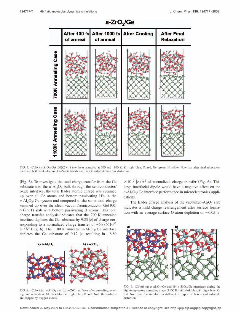
The DFT annealing of vacuum/a-Al2O3 surfaces revealsa pronounced interface chemical segregation with Al atomsmigrating into the bulk and O atoms migrating to the surfaceto create O surface capping �Fig. 8�a��. This phenomenon ofoxygen enrichment of oxide/vacuum interfaces was previ-ously reported for classical MD simulations of thevacuum/a-Al2O3 interfaces,30 and by first-principle simula-tions of the �0001� interfaces of �- and �001� interfaces ofcrystalline �-alumina with vacuum.37,38 The surface segrega-tion at the vacuum/a-Al2O3 interface can be explained by thedifferent geometries of O and Al bonds. In a-Al2O3, bulk Alatoms predominantly have four or five nearest neighbors�Fig. 2�. The Al atom located at the oxide-vacuum interfacewould likely have a lower number of neighbors thereby in-creasing the total energy of the system. The O atoms pre-dominantly have only two or three neighbors in the a-Al2O3
bulk �Fig. 2�; therefore, they will more likely accommodatebonding at the vacuum/oxide interface without significantlychanging the total energy.
The a-Al2O3 /Ge interfaces annealed at 700 and 1100 Kdemonstrate very similar interface oxygen enrichment com-pared to the vacuum/a-Al2O3 interface �Fig. 6�. Fora-Al2O3 /Ge interfaces, oxygen atoms migrate to the semi-conductor interface and Al atoms migrate into the bulk oxideresulting in interfacial bonding exclusively through Al–O–Ge bonds with no or very few O–Al–Ge bonds.39 ThisO-rich bonding is present even during the high-temperatureannealing stage �Figs. 6 and 9�a��. The interface segregationoccurs during the first 100 fs �10% of the whole annealingtime�, indicating the DFT time scale used is sufficient toobserve this phenomenon �Fig. 6�. Increasing the interfacialannealing temperature from 700 to 1100 K has no effect onthis interface chemical migration.
Interfacial bonding exclusively through Al–O–Ge bondscan result in strong interface polarity; this is not a desiredcharacteristic as significant charge transfer has a negativeimpact on device performance. To verify and quantify thiseffect, a Bader charge analysis was performed.40,41 TheBader charge analysis indicates that for the a-Al2O3 /Ge in-terfaces annealed at 700 and 1100 K, the Ge atoms bondedto O lose, on average, about 0.7–1.0 e of atomic charge
FIG. 6. �Color� a-Al2O3 /Ge�100��2�1� interfaces annealed at 700 and 1100 K. Al: blue, O: red, Ge: green, H: white. Note that after final relaxation theinterfaces are dominated by O–Ge bonds and the Ge substrate is distorted.
124717-6 E. A. Chagarov and A. C. Kummel J. Chem. Phys. 130, 124717 �2009�
Downloaded 26 May 2009 to 132.239.156.140. Redistribution subject to AIP license or copyright; see http://jcp.aip.org/jcp/copyright.jsp
�Fig. 6�. To investigate the total charge transfer from the Gesubstrate into the a-Al2O3 bulk through the semiconductor/oxide interface, the total Bader atomic charge was summedup over all Ge atoms and bottom passivating H’s in thea-Al2O3 /Ge system and compared to the same total chargesummed up over the clean vacuum/semiconductor Ge�100���2�1� slab with bottom passivating H atoms. This totalcharge transfer analysis indicates that the 700 K annealedinterface depletes the Ge substrate by 9.23 e of charge cor-responding to a normalized charge transfer of −6.88�10−2
e /Å2 �Fig. 6�. The 1100 K annealed a-Al2O3 /Ge interfacedepletes the Ge substrate of 9.12 e resulting in −6.80
�10−2 e /Å2 of normalized charge transfer �Fig. 6�. Thislarge interfacial dipole would have a negative effect on thea-Al2O3 /Ge interface performance in microelectronics appli-cations.
The Bader charge analysis of the vacuum/a-Al2O3 slabindicates a mild charge rearrangement after surface forma-tion with an average surface O atom depletion of 0.05 e
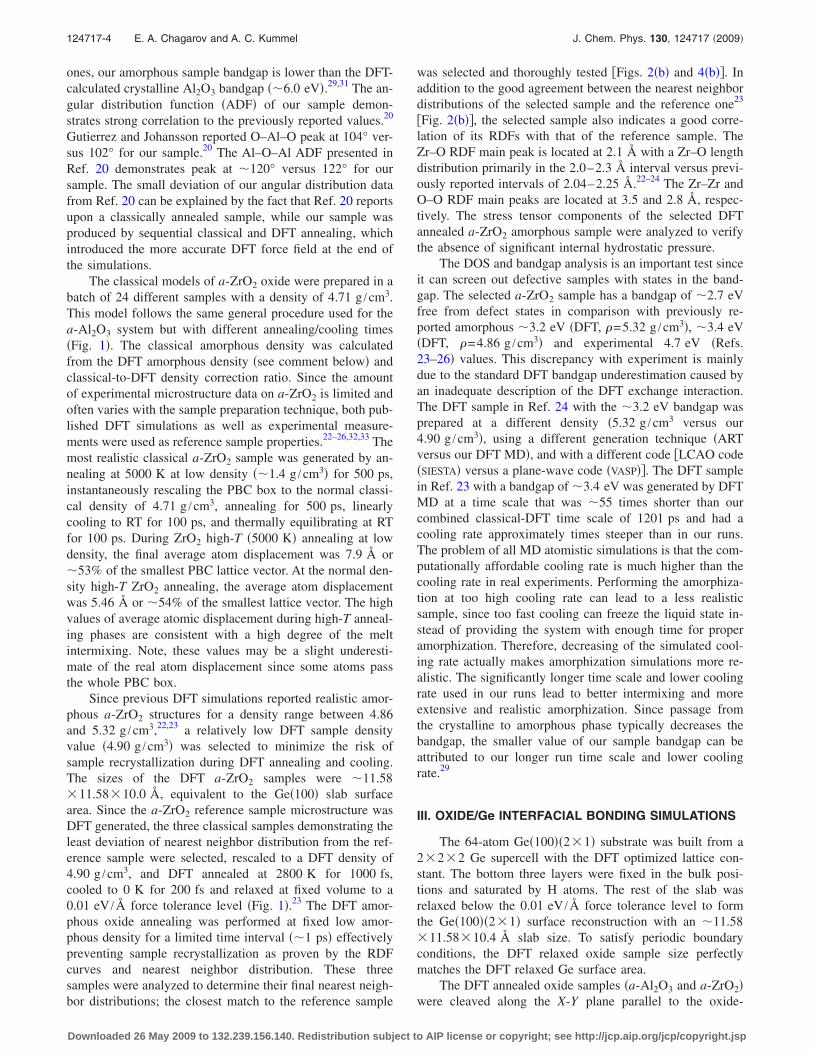
FIG. 7. �Color� a-ZrO2 /Ge�100��2�1� interfaces annealed at 700 and 1100 K. Zr: light blue, O: red, Ge: green, H: white. Note that after final relaxation,there are both Zr–O–Ge and O–Zr–Ge bonds and the Ge substrate has low distortion.
FIG. 8. �Color� �a� a-Al2O3 and �b� a-ZrO2 surfaces after annealing, cool-ing, and relaxation. Al: dark blue, Zr: light blue, O: red. Note the surfacesare capped by oxygen atoms.
FIG. 9. �Color� �a� a-Al2O3 /Ge and �b� a-ZrO2 /Ge interfaces during thehigh-temperature annealing stage �1100 K�. Al: dark blue, Zr: light blue, O:red. Note that the interface is different in types of bonds and substratedistortion.
124717-7 Ab initio molecular dynamics simulations J. Chem. Phys. 130, 124717 �2009�
Downloaded 26 May 2009 to 132.239.156.140. Redistribution subject to AIP license or copyright; see http://jcp.aip.org/jcp/copyright.jsp
in comparison with the slab in-bulk oxygens �Fig. 8�a��.However, since the slab thickness is only 7.5 Å, this sur-face depletion may differ for thicker slabs.
The DFT annealing of the vacuum/a-ZrO2 slab with twovacuum interfaces reveals trends similar to thevacuum/a-Al2O3 slab dynamics �Fig. 8�. The oxygen atomsmigrate to the surface creating O-rich surface capping, whileZr atoms migrate into the bulk. In the a-ZrO2 bulk, Zr pre-dominantly has six or seven nearest neighbors �Fig. 2�. TheZr atom located at the oxide-vacuum interface would likelyhave a lower number of nearest neighbors thereby increasingthe total energy of the system. The bulk O atoms predomi-nantly have only three or four nearest neighbors in thea-ZrO2 bulk �Fig. 2� and will more likely accommodate thevacuum/oxide interface geometry without significantly in-creasing the total energy of the system.
The a-ZrO2 /Ge interfacial bonding is different from thevacuum/a-ZrO2 interfacial bonding. Whereas the oxide/vacuum interface demonstrates O-enrichment, thea-ZrO2 /Ge interfaces annealed at 700 K and 1100 K haveroughly equal numbers of Zr–O–Ge and O–Zr–Ge bonds inthe interface region �Fig. 7�. During annealing �700 or1100 K�, �Fig. 9�b��, the interface has approximately 1.5times more long Zr–Ge bonds �empirical length 3 Å� thanshort O–Ge bonds �empirical length 2 Å� with oxygen at-oms tending to bridge between Zr atoms �Fig. 9�b��. How-ever, during the final relaxation, the interface is compacted;the average interatomic distance decreases and more shortO–Ge bonds are formed roughly balancing the number oflong Zr–Ge bonds. Increasing the annealing temperaturefrom 700 to 1100 K has no significant effect on interfacebond populations �Fig. 7�. The high number of Zr–Ge bondswill likely create states in the bandgap that will pin the Fermilevel. The electronic structure of a-ZrO2 bonded to ana-GeO2 passivation layer on Ge have been calculated andindicated significant improvement of the stack electronicstructure.42
The fact that the a-ZrO2 /Ge interface has bidirectionalbonding in contrast to the unidirectional bonding of thea-Al2O3 /Ge interface has a significant effect on the interfacepolarity. The terms “unidirectional” and “bidirectional” areemployed to differentiate between interface in which all thebond dipoles point in the same direction versus one in whichbond dipoles point in opposite directions.
The Bader charge analysis of a-ZrO2 /Ge interfaces an-nealed at two different temperatures indicates that Ge atomsbonded to O lose about 0.3–0.9 e of atomic charge, whileGe atoms bonded to Zr gain about 0.2–0.7 e. The totalcharge depletion in the Ge substrate is estimated to be 0.40e or −2.98�10−3 e /Å2 for the 700 K annealed interface�Fig. 7�, and 0.34 e or −2.53�10−3 e /Å2 for the 1100 Kannealed one �Fig. 7�. Therefore, the total charge transferthrough the interface is about 23–27 times smaller fora-ZrO2 /Ge compared to a-Al2O3 /Ge consistent with the factthat the a-ZrO2 /Ge interface with O–Zr–Ge and Zr–O–Gebonds has compensating bond dipoles, while the a-Al2O3 /Geinterface has only unidirectional Al–O–Ge bond dipoles.
The Bader charge analysis of the a-ZrO2 slab in vacuum
indicates a mild charge depletion of the vacuum/oxide sur-face O atoms on average by 0.09 e in comparison withthe bulk oxygens in the slab �Fig. 8�b��.
B. Coordination changes induced by bonding at theoxide/semiconductor and vacuum/oxide interfaces
The interfacial coordination number distribution has adirect impact on electronic properties and microelectronicsdevice performance. To understand how the oxide structureis altered by bonding to Ge, the change in surface coordina-tion after bonding to Ge can be compared for thea-Al2O3 /Ge and a-ZrO2 /Ge interfaces. Note that in com-puter simulations the “coordination” value is determined bythe number of nearest neighbors within a certain cutoff ra-dius; this can result in small differences in coordination num-ber distributions determined by direct imaging of electrondistributions. Below the coordination numbers of the surfaceatoms at the vacuum/oxide and oxide/semiconductor inter-faces are compared to determine how the semiconductor per-turbs the coordination numbers of the surface oxide atoms.
The a-Al2O3 vacuum/oxide interface with surface oxy-gen enrichment has a roughly equal partition of two- andthree-coordinated surface oxygen atoms, while the Al atomsclosest to the surface and forming bonds to surface O atomshave 15% of three-fold, 75% of four-fold and 10% offive-fold coordinated atoms �Fig. 8�a��. The Ge�100��2�1�vacuum/semiconductor surface dimer atoms have a coordi-nation of 3.
The stacking of a-Al2O3 on Ge�100��2�1� reconstruc-tion perturbs the Ge substrate coordination distribution buthas no significant effect on the O interface coordination dis-tribution both for the 700 and 1100 K annealed cases. Forthe 700 K a-Al2O3 /Ge annealed interface �Fig. 6�, Ge atomsswitch from 100% three-fold coordination at the vacuum in-terface to 45% three- and four-fold coordination and 10%two-fold coordination. The two-fold coordinated Ge atomsare those which are pulled out of the substrate and arebonded only to O atoms. Some of Ge dimer atoms do notform bonds to the oxide, thereby preserving three-fold coor-dination. The high-temperature annealed interface �1100 K,Fig. 6� has only minor deviations in the interfacial Ge coor-dination distribution in comparison with the low-temperatureannealed case �700 K, Fig. 6� having an equal partition ofthree- and four-coordinated Ge atoms with no two foldedones; the absence of two fold coordinated Ge atoms at hightemperature compared to low temperature is probably justdue to the limited sample size. The oxygen atoms in thea-Al2O3 /Ge interface region for both annealing temperatureshave nearly identical total coordination numbers �i.e., O–Alplus O–Ge� as the oxygen at the vacuum/oxide a-Al2O3 sur-face: roughly equal partition of two- and three-coordinatedoxygens. A few O atoms diffuse into subsurface Ge to formtwo bonds to Ge atoms thereby breaking Ge–Ge bonds.Since the Al atoms do not make bonds to the Ge substrate,the Al atoms in a-Al2O3 closest to the Ge interface retain thecoordination distribution of subsurface Al atoms at thea-Al2O3/vacuum interface.
The vacuum/oxide a-ZrO2 surface has an approximately
124717-8 E. A. Chagarov and A. C. Kummel J. Chem. Phys. 130, 124717 �2009�
Downloaded 26 May 2009 to 132.239.156.140. Redistribution subject to AIP license or copyright; see http://jcp.aip.org/jcp/copyright.jsp

equal partition of two- and threefold coordinated O atoms,the same as the a-Al2O3 slab. The subsurface Zr atomsbonded to the surface oxygens exhibit 37% five-coordinateand 63% six-coordinate partitions �Fig. 8�b��. In contrast,the a-ZrO2 /Ge interface has a roughly equal partition oftwo- and three-coordinated O �Fig. 7�, demonstrating thatstacking to the Ge substrate does not effect the interfacial Ocoordination distribution. However, the Ge coordination dis-tribution is altered by the stacking from threefold to an equalpartition of three- and fourfold for the surface atoms similarto a-Al2O3 /Ge. There are no twofold coordinated Ge atomsfor the 700 and 1100 K annealed a-ZrO2 /Ge interfaces. Theinterface Zr atoms forming bonds to Ge have a wide coordi-nation distribution between 4 and 7 �note this includes Zr–Oand Zr–Ge bonds�; this is broader than the Zr coordinationdistribution at the a-ZrO2/vacuum interface. Increasing theannealing temperature from 700 to 1100 K does not signifi-cantly affect the a-ZrO2 /Ge interface coordination.
C. Interfacial roughness induced by bonding at theoxide/semiconductor interface
The interface roughness with large intermixing can havea deleterious impact on carrier mobility and total device per-formance. The DFT simulations demonstrated higher Gesubstrate deformation and higher intermixing fora-Al2O3 /Ge interfaces in comparison with a-ZrO2 /Ge �Figs.6 and 7�. To quantify Ge substrate deformation, the averageGe positional deviation per horizontal layer with respect tothe relaxed clean Ge�100��2�1� slab was calculated using
the following norm: �R̄i= �1 /Ni�� jR̄j − R̄0j, where Ni is the
number of Ge atoms in horizontal layer i, R̄j and R̄0j arecoordinates of Ge atom j belonging to the horizontal layer iafter the interface relaxation and in the initial relaxed cleanGe�100��2�1� slab, while index j goes along every Ge atomin horizontal layer i. The Ge�100��2�1� slab has eight at-oms per layer. The average Ge deviation per layer is pre-sented in Fig. 10. The first three layers have zero deviationsince they are fixed in their bulk positions.
The quantified deformation data presented in Fig. 10 areconsistent with greater Ge substrate deformation at thea-Al2O3 /Ge interface than at the a-ZrO2 /Ge interface. Forthe 700 K annealed a-Al2O3 /Ge interface, the surface dimeratoms �layers 8 and 9� deviate on average by 1.3 and 2.5 Å,respectively, while the same Ge dimer atoms in thea-ZrO2 /Ge interface deviate on average by only 1.0 and0.9 Å �Fig. 10�. The same general trend is maintained for theother subsurface layers �Fig. 10�. Some of Ge dimer atomsare pulled up by the a-Al2O, thereby distorting the Ge sur-face and creating vacancies that facilitate O diffusion.
Increasing the annealing temperature to 1100 K pre-serves the larger deformation in the a-Al2O3 /Ge interfaceversus a-ZrO2 /Ge with dimer atom deviations of 1.7 Å,1.5 Å �a-Al2O3 /Ge� versus 0.7 Å, 1.2 Å �a-ZrO2 /Ge�. Fora-ZrO2 /Ge, increasing the annealing temperature from700 to 1100 K leaves the Ge substrate deformation un-changed �Fig. 7�. Conversely, for a-Al2O3 /Ge interfaces, in-creasing the annealing temperature from 700 to 1100 K cre-ates substantially greater Ge substrate deformation �Fig. 6�.In addition, annealing at higher temperature �1100 K� leadsto microcavity formation in a-Al2O3 oxide �Fig. 6�.
Analysis of the a-ZrO2 /Ge interface evolution indicatessubstantial deformation of the Ge substrate during annealingat 1100 K �Fig. 7�. However, subsequent final relaxationleads to significant recovery of the Ge substrate regular lat-tice structure. This is mainly due to the absence of atomicdiffusion from oxide into the substrate in a-ZrO2 /Ge system,which otherwise would create lattice deformation centers.Although for both a-Al2O3 /Ge and a-ZrO2 /Ge interfacesDFT MD annealing was started with bulk oxide samples incontact with Ge substrate, the final outcome of the simula-tions revealed substantial differences in interface bondingand deformation.
D. Mechanical and thermochemical properties ofa-Al2O3 versus a-ZrO2 responsible for differences insemiconductor bonding
1. Mechanical property differences
The smaller substrate deformation at the a-ZrO2 /Ge in-terface compared to the a-Al2O3 /Ge interface is consistentwith relative bulk moduli and the ADFs. The calculated ADFfor bulk a-Al2O3 and a-ZrO2 samples have a standard devia-tion of 23.7° for O–Al–O angles, while O–Zr–O angles havea standard deviation of 28.7° indicating a larger flexibility ofbond angles in a-ZrO2, consistent with less deformation andintermixing in a-ZrO2 /Ge interfaces in comparison witha-Al2O3 /Ge ones �Figs. 6 and 7�. The a-ZrO2 has a lowerDFT-calculated bulk modulus �B=77.9 GPa� than a-Al2O3
�B=96.9 GPa� �a-Al2O3 experimental value −89.3 GPa �Ref.43�� but both are larger than the DFT calculated bulk modu-lus of crystalline Ge �57.8 GPa�. The difference between theDFT calculated crystalline Ge and a-ZrO2 bulk moduli is35% compared to the difference between Ge and a-Al2O3 of68% again consistent with smaller deformation of Ge at thea-ZrO2 /Ge interface compared to the a-Al2O3 /Ge interface.
FIG. 10. �Color online� Average Ge deviation per layer after interface for-mation. Layers 1–3 are fixed layers of Ge substrate. Layers 8–9 are surfacedimer layers of the Ge�100��2�1� surface reconstruction.
124717-9 Ab initio molecular dynamics simulations J. Chem. Phys. 130, 124717 �2009�
Downloaded 26 May 2009 to 132.239.156.140. Redistribution subject to AIP license or copyright; see http://jcp.aip.org/jcp/copyright.jsp

2. Thermochemical property differences
The possible interfacial solid state reactions were esti-mated from the Gibbs free energy change in O transfer fromthe oxide to the substrate to form GeO2 or GeO oxides. Cre-ation of GeO2 oxide was found to be endothermic and re-quired 537.1 and 520.6 kJ /mol �normalized to one GeO2
unit� for a-Al2O3 /Ge and a-ZrO2 /Ge interfaces, respec-tively. Creation of GeO interfacial oxides is also endo-thermic, requiring 296.7 and 288.4 kJ /mol �normalized toone GeO unit� for a-Al2O3 /Ge and a-ZrO2 /Ge interfaces,respectively.36 The temperature-dependent term is not sig-nificant enough to cause reaction exothermicity at reasonableprocessing temperatures. Note that interfaces often are notstoichiometric, which can significantly affect Gibbs energychange for interfacial reactions in oxygen-rich conditions.Therefore, the presented values can be considered only asestimates for interfacial oxide GeOx �1x2� formation.The fact that O transfer reaction enthalpies from a-Al2O3 anda-ZrO2 to Ge to form GeO or GeO2 are endothermic andclose in value for a-Al2O3 and a-ZrO2 indicates that inter-mixing at the a-Al2O3 /Ge interface should be attributedmainly to dynamic rather than thermodynamic phenomena.
3. Kinetic property differences
MD simulations reveal that subsurface diffusion of Oatoms can be one of the causes of interface deformation andintermixing. Oxygen diffusing into Ge creates centers of Gelattice deformation. The bulk thermodynamics of oxygen dif-fusion into Ge is very similar for a-Al2O3 /Ge anda-ZrO2 /Ge interfaces; however, the kinetics and surfacethermodynamics are quite different. When the oxide pulls Geatoms up, vacancies are created for O diffusion �Fig. 6� be-cause gross distortion of the Ge lattice creates partially filledGe dangling bonds that effectively lower the activation bar-rier for oxygen diffusion. Since a-Al2O3 more readily dis-torts the Ge lattice than a-ZrO2, the former creates moreoxygen diffusion despite any difference in bulk oxygen dif-fusion thermodynamics.
E. Discussion of possible statistical errors
To double check that the DFT-MD interface kinetic dif-ference between a-Al2O3 /Ge and a-ZrO2 /Ge are not justdue to random differences between a small number ofDFT-MD runs, it is informative to estimate average maximaloxide atom shift in interface region during DFT MD runs.The shift was estimated along the X-Y plane parallel to theinterface. The statistics were obtained from an 2.5 Å thickoxide layer contacting semiconductor substrate containing20–25 “oxide interface” atoms. For 700 K annealeda-Al2O3 /Ge interfaces, an average maximal shift of interfaceoxide atoms was 2.7 Å, while for 1100 K annealeda-Al2O3 /Ge interface it was 4.0 Å. The same analysis for700 K annealed a-ZrO2 /Ge interface indicated averagemaximal shift of 1.6 Å, while for 1100 K annealeda-ZrO2 /Ge interface it was 2.6 Å. These results are con-sistent with faster kinetics for higher temperature annealingcases and with larger deformation in a-Al2O3 /Ge interfacesin comparison with a-ZrO2 /Ge ones. These average maximal
shift statistics compared to DFT Ge–Ge bondlength of2.5 Å demonstrate that during DFT MD runs, oxide inter-facial atoms very effectively sample Ge�100��2�1� 2D sur-face pattern. This effective sampling of Ge�100��2�1� sur-face pattern indicates, that initial atomic arrangement haslimited effect on final atomic configuration of investigatedinterfaces. The average maximal shift during annealing rap-idly increases approximately for the first 500–600 fs, thenstabilizes; finally in the last 200 fs it looks nearly constant.The stabilization of the atomic position after 600–800 fs in-dicates that the time scale is enough to stabilize the oxide atthe interface.
DFT MD is a very accurate simulation technique, whichrequires significant computational resources and time. Al-though better statistics can be obtained by performing manysimulations with different samples and initial configurations,the very high cost of DFT MD runs make this impracticalwithin reasonable time at modern computational facilities.The generation of another realistic classical sample and itssubsequent DFT annealing would provide a sample with dif-ferent atomic arrangements, but very similar averaged bulkproperties such as RDFs, coordination distributions, and av-erage coordination numbers because only these sampleswould pass realism test by comparison to the referencesample. The initial interface atomic arrangement has widervariation from system to system. However investigation ofamorphous/crystalline interface makes the initial configura-tion more robust and general since amorphous surface withits high level of randomization inherently provides enhancedlevel of generality by sampling much more possibilities ofinitial interatomic bonding in configuration space of oxide/semiconductor interface. Performing DFT MD at finite tem-perature adds a whole new dimension of realism by probingdifferent interface bonding configurations over time effec-tively sampling Ge�100��2�1� two-dimensional �2D� sur-face pattern. The fact that our results demonstrate good cor-relation to experimental data and interface annealing at theelevated �1100 K� temperature leads to the same qualitativeresults as interface annealing at 700 K support generality andreliability of the presented a-Al2O3 /Ge and a-ZrO2 /Ge in-terface evolution simulations.
F. Discussion of simulation methods
There are several simulation approaches which poten-tially can be considered for modeling of amorphous oxide-semiconductor interfaces:
�a� Kinetic Monte Carlo �KMC� simulations.44–46 KMCsimulations can simulate the time evolution of certainprocesses occurring with a given rate. However, theserates are input variables for KMC simulations and areoften obtained from DFT simulations of the energy bar-riers for certain set of system transitions.
�b� DFT MD simulations with oxide atoms randomly bom-barding the semiconductor surface trying to simulateatom-by-atom deposition. However, nearly all oxidesincluding Al2O3 and ZrO2, evaporate incongruently sothis is just a approximate model for molecular beamdeposition grown oxide/semiconductor interfaces.
124717-10 E. A. Chagarov and A. C. Kummel J. Chem. Phys. 130, 124717 �2009�
Downloaded 26 May 2009 to 132.239.156.140. Redistribution subject to AIP license or copyright; see http://jcp.aip.org/jcp/copyright.jsp

�c� DFT MD simulations with previously prepared bulkamorphous sample stacked to the semiconductor sur-face and relaxed or annealed-cooled-relaxed as it waspresented in this paper.
Each of these methods has its own advantages and dis-advantages, which should meet certain strict criteria of ap-plicability. One of the major criteria is realism, computa-tional efficiency, and achievable simulated time scale.
KMC simulations are relatively computationally effi-cient, provide long time scale modeling and could simulateatom-by-atom deposition. However for atomistic modelingof oxide-semiconductor interface evolution, KMC wouldprovide lower accuracy than DFT MD, since KMC simula-tions replace the true atomic dynamics with statisticallyequivalent kinetics. The KMC simulations are based on a setof energy barrier calculations and associated rates for variousconfigurations and transitions between the configurations.The DFT MD simulations presented in this paper indicatedsignificant deformation in the substrate, interface, and oxideregions with a very large number of degrees of freedom. Anattempt to reproduce a realism of such DFT MD simulationswith 3D KMC would require taking into account an unreal-istic number of atomic configurations, transition barriers be-tween them and DFT-calculated activation energies.
Method B, DFT-MD simulations with oxide atoms ran-domly bombarding the semiconductor surface cannot accu-rately model experimental oxide-semiconductor interfacegrowth for three reasons. �a� With the exception of LaAl2O3,nearly all gate oxide evaporate incongruently so to form stoi-chiometric films using molecular beam deposition, a secondoxygen source must be employed or postdeposition anneal-ing must be employed. �b� Quantitative analysis of the timescale needed to deposit 100 atoms of oxide at realistic ex-perimental deposition rate shows that it would require manyorders of magnitude longer time scale than picoseconds,which modern DFT MD can simulate. The fastest MBEdeposition rate is 0.1 ML /s,47 the fastest metal organicchemical vapor deposition �MOCVD� is 3 ML /s �Ref. 48�and the fastest sputtering deposition is 1 ML /s.49 �c� Mostgate oxides are deposited by atomic layer deposition, notmolecular beam deposition.
Although methods �a� and �b� are able to simulate atom-by-atom deposition they raise significant concerns aboutamorphous film realism. Method �c� described in this paperprovides elaborate system of checks to verify high quality ofthe utilized amorphous sample. Based on such consider-ations, it is reasonable to conclude that the method �c� whichstacks bulk oxide on the semiconductor substrate with sub-sequent relaxation or annealing-cooling-relaxation �as pre-sented in this paper� provides the most realistic computa-tional approach affordable for modern computationalfacilities. Although it has some disadvantages, it has beensuccessfully used by many groups for atomistic simulationsof oxide-semiconductor interfaces. Tse and Robertson suc-cessfully utilized this approach for modeling of ZrO2 /Ge.4
Peacock et al.,50,51 Puthenkovilakam et al.,52,53 Fonseca etal.,54 and Dong et al.55 successfully applied it to simulationsof ZrO2 /Si, ZrSiO4 /Si and HfO2 /Si interfaces. Zhang et al.,8
Peacock and Robertson,56 and Forst et al.,57 and Robertsonand Peacock58 used it for modeling of SrTiO3 /Si interface.Broqvist and co-workers used it for simulations ofa-HfO2 /a-SiO2 /Si and HfO2 /SiO2 stacks.10,34,59
G. Comparison to experimental a-Al2O3/Ge anda-ZrO2/Ge interfaces responsible for differences insemiconductor bonding
The DFT-MD simulations make several predictionswhich can be compared to experiments. �1� Under idealdeposition conditions, the ZrO2 /Ge interface should be moreabrupt than the a-Al2O3 /Ge interface. �2� For a-ZrO2 /Geand a-Al2O3, the interfacial bonds are polar covalent andboth the oxide and substrate atoms should retain nearly bulk-like electron binding energy in x-ray photoelectron spectros-copy �XPS�. For comparison to experiment, the differencesin electron charge associated with atoms at the oxide/semiconductor interface and in the bulk were calculated bycomparing the Bader charges of the oxide/Ge interface atomswith the same atoms in bulk oxide and Ge. For a-ZrO2 /Ge,the changes in Bader charge are between +0.05 and +0.32efor Zr, between −0.06 and +0.03e for O, between −0.5eand +0.3e for Ge; a negative change in Bader charge meansan electron charge depletion at a particular atom. Thereforefor a-ZrO2 /Ge, it would be predicted the XPS peaks for theinterfacial oxide would be bulk-like and a slight broadeningmight be observed for interfacial Ge. For a-Al2O3 /Ge, thechanges in Bader charge are +0.03e to +0.2e for Al,−0.3e to −0.1e for O, and −0.8e to −0.4e for Ge. There-fore, for a-Al2O3 /Ge, it would be predicted that the XPSpeaks for the interfacial oxide would be bulklike and a verysmall Ge+1 component should be observed for interfacial Ge.As a control, we also calculated the Bader charge change ina thin amorphous GeO2 layer. In a 2 ML GeO2 layer, the Geatoms have charges between −1e and −2e compared to thebulk consistent with formation of mostly of a mixture ofGe+1 and Ge+2.42 Formation of the a-Al2O3 /Ge interfaceleads to much greater total charge transfer from Ge to theoxide than formation of the a-ZrO2 /Ge interface, and theinterfacial and bulk oxide atoms in the a-Al2O3 /Ge stackdemonstrate very small deviation in Bader charges; this im-plies that the charge pulled into a-Al2O3 oxide after interfaceformation is distributed with a high degree of homogeneitywithin the oxide.
To compare the DFT-MD simulations to experiment, theoxide deposition method must be considered since the oxidedeposition method can disrupt the interface. Unlike silicon,annealing of high-k /Ge interfaces need not produce an inter-layer oxide formation;60,61 therefore, interlayer oxide forma-tion is specific to the oxide deposition technique. There threecommon gate oxide deposition methods are �a� atomic layerdeposition �ALD� or MOCVD; �b� sputter deposition; �c�oxidation of a metal film.
Most studies on gate oxide deposition on Ge employALD. Nearly all papers show the need to remove the nativeoxide prior to ALD because the native oxide is highly defec-tive. On both Si and Ge, the ALD process is almost alwaysinitiated using one or more pulses of water vapor. Thesewater pulses disrupt the Ge surface, create an oxide with a
124717-11 Ab initio molecular dynamics simulations J. Chem. Phys. 130, 124717 �2009�
Downloaded 26 May 2009 to 132.239.156.140. Redistribution subject to AIP license or copyright; see http://jcp.aip.org/jcp/copyright.jsp

high hydroxyl content, and/or create an oxide in which theGe has a large range of valence states. Both hydroxylcontent62 and low valence state GeOx are strongly correlatedwith a high interfacial trap density.63 To mitigate this prob-lem, many research groups passivate the surface prior toALD oxide deposition using either NH3,64 ozone,65 or highpressure O2 �Refs. 66 and 67� to form either a GeO2 layer ora GeON passivation layer which is only 1 nm thick and con-tains only Ge+4 with a low OH content. ALD oxides typicallyare slightly nonstoichiometric so their insulating propertiesare improved by postdeposition annealing �PDA�. For PDAabove 500 °C, germanium monoxide is observed to diffuseinto the oxide and accumulate on the surface of the oxide dueto the reaction GeO2+Ge→2GeO.68,69 The effect of a pas-sivation layer on interfacial bonding and electronic structurebetween an amorphous oxide and Ge�100� will be addressedin a future paper. Due to the thermal instability and lowdielectric constant of GeO2, it is desirable to directly bondoxide to Ge �Ref. 70� using either sputter or electron beamdeposition techniques.
In sputter deposition, an oxide target is bombarded withenergetic ions and secondary vaporized oxide particles aredirected at the substrate. It is extremely rare for an oxide toevaporate congruently so O2 is always present in the depo-sition chamber during oxide sputter deposition; thereforesome GeOx formation will occur and the lattice will be dis-rupted. Kamata et al.61 formed ZrO2 /Ge and HfO2 /Ge inter-faces by sputter deposition from an oxide target onto etchedGe wafers. TEM showed that the as-deposited wafers had asmall interface layer �1 nm of probably GeOx� but annealingto 500 °C completely removed the interface layer forZrO2 /Ge and an abrupt smooth interface was formed withoutdistortion in the Ge substrate. The interface layer could havebeen formed in the sputter deposition process because, asnoted above, oxygen is present during sputter depositioneven from an oxide target. The absence of an interfacial layerafter annealing is consistent with the ZrO2 /Ge interface be-ing thermodynamically stable as predicted by the DFT-MDsimulations.
Electron beam oxide deposition is employed for gate ox-ide formation on Ge using two methods. �i� An oxide can bedirectly evaporated by an electron beam. Nearly all oxidesevaporate incongruently resulting in O2 generation; the O2
can react with Ge disrupting the lattice. �ii� A thin metal suchas Hf or Zr is deposited at low temperature on Ge and oxi-dized using ozone.71 Since the metal is more reactive to O3
than Ge and metal oxide are reasonably good diffusion bar-riers, this can result in the formation of abrupt oxide/Ge in-terfaces.
Data from three studies are strongly consistent with theDFT-MD simulations: �1� Chui et al.72 using XPS to studythe bonding between a-ZrO2 /Ge where ZrO2 was depositedby uv ozone oxidation of a sputter deposited Zr at 300 K ona HF etched Ge�100� surface. No Ge was detected inside theZrO2. The interfacial GeOx layer was only 1.9–3.6 Å thickand was mainly Ge+1 consistent with formation of a thinamorphous 2 ML GeO2 layer with the charge distributionpredicted above. �2� Chi et al.73 used both transmission elec-tron microscopy �TEM� and angle resolved XPS study the
bonding between a-ZrO2 /Ge where ZrO2 was deposited byuv ozone oxidation of a sputter deposited Zr at 50 °C on ade-ionized water-rinsed Ge�100� surface. The Zr films were10, 20, and 30 Å thick. For the 30 Å films, all the Zr was inthe Zr+4 oxidation state of ZrO2, while for Ge, all the atomswere in the Ge+0 oxidation state of bulk Ge consistent withthe DFT-MD calculations. The TEM images of the 30 Åa-ZrO2 /Ge show an abrupt interface consistent with theDFT-MD calculations. �3� Kamata et al.61 formed ZrO2 /Geand HfO2 /Ge interfaces by sputter deposition from oxidetarget onto etched Ge wafers. TEM showed that after anneal-ing to 500 °C, there was an abrupt smooth interface. We notethat the annealing induced crystallization of the a-ZrO2.These results are consistent with the absence of intermixingobserved in the DFT-MD calculations.
Data from two studies are consistent with the DFT-MDresults for a-Al2O3 /Ge�100�: �1� Malafsky74 studied thedeposition of Ge on crystalline Al2O3. The Ge forms crystal-line clusters producing an interface similar to the one in theDFT-MD studies. For submonolayer coverages, Ge is ob-served by XPS in the Ge+4 oxidation state consistent withbonding selectively to oxygen atoms on the Al2O3 surfaceconsistent with the DFT-MD results on bonding; the anoma-lously high experimental oxidation state of the Ge is due tothese Ge atoms being adatoms on an oxide surface instead ofbulk Ge atoms making multiple Ge–Ge bonds. For all cov-erages, the experimental Al and O peaks are bulk-like con-sistent with the small shifts in charge calculated with theDFT-MD simulations. For coverages above 2 ML, the ex-perimental XPS spectrum consisted almost entirely of Ge inGe+0 consistent the small shifts in charge calculated with theDFT-MD simulations. �2� Bellenger et al.75 studied the for-mation of a-Al2O3 /Ge using Al evaporation onto Ge�100� inthe presence of atomic oxygen. TEM images show an amor-phous oxide with an abrupt interface to Ge without an obvi-ous interlayer. XPS studies show the Al peak is unshiftedcompared to that from Al2O3 consistent with the chargechanges calculated with DFT-MD. The Ge XPS spectrumshows a small amount of Ge+2, Ge+3, and Ge+4 consistentwith Ge–O bonds over a region of less than 8 Å. This greaterintermixing for Al2O3 /Ge compared to ZrO2 /Ge is consis-tent with the DFT-MD calculations, but Bellenger et al.75
simultaneously exposed the surface to Al and O atoms whichwould tend to place a bit more oxygen at the interface thanoxidation of an Al film so the comparison to the DFT-MDa-ZrO2 /Ge interfaces cited above is slightly biased.
VI. SUMMARY AND CONCLUSIONS
We presented DFT MD simulations of a-Al2O3 anda-ZrO2 interfaces with vacuum and with a Ge�100��2�1�substrate at two different annealing temperatures �700 and1100 K�. Realistic amorphous Al2O3 and ZrO2 samples weregenerated with a hybrid classical-DFT melt and quench ap-proach, thoroughly tested and demonstrated to have goodcorrelation with experimental results and computer simula-tions.
The simulations of a-Al2O3 and a-ZrO2 vacuum/oxidesurfaces indicated strong surface chemical selectivity with O
124717-12 E. A. Chagarov and A. C. Kummel J. Chem. Phys. 130, 124717 �2009�
Downloaded 26 May 2009 to 132.239.156.140. Redistribution subject to AIP license or copyright; see http://jcp.aip.org/jcp/copyright.jsp

atoms migrating to the surface and Al and Zr atoms migrat-ing into the bulk, creating surface oxygen capping. Thestacking of a-Al2O3 to the Ge�100��2�1� substrate pre-serves this trend creating an O-enriched interface bonded ex-clusively through Al–O–Ge bonds with no or few O–Al–Geones. The stacking of a-ZrO2 to the Ge substrate and inter-face annealing revealed different behavior resulting inroughly equal numbers of Zr–O–Ge and O–Zr–Ge bonds.During the high-temperature anneal, the a-ZrO2 /Ge interfaceexpansion favors longer Zr–Ge bonds with O atoms bridgingbetween Zr ones. However, cooling and final relaxation re-sult in a more compact interface creating more O–Ge bondswhich roughly balance the number of Zr–Ge ones. Due tohigh bond selectivity, a-Al2O3 /Ge interfaces have strong in-terface polarity and charge transfer from Ge to a-Al2O3 ox-ide. Conversely, the a-ZrO2 /Ge interfaces have roughlyequal numbers of Zr–O–Ge and O–Zr–Ge bonds and23–27 times less charge transfer.
The effect of the interface annealing temperature wasinvestigated by studying two annealing temperatures: 700and 1100 K. The a-ZrO2 /Ge interface reveals no significantdeformation or intermixing at either annealing temperature.Conversely, the a-Al2O3 /Ge interface shows a higher inter-face roughness for the higher temperature �1100 K� annealedinterface than for the low-temperature �700 K� one.
A comparison of interface deformation indicates a muchstronger deformation and intermixing in a-Al2O3 /Ge inter-faces than in a-ZrO2 /Ge ones. This is consistent with thedifference in the bulk moduli and ADFs of bulk a-Al2O3 anda-ZrO2 oxides. The a-Al2O3 has higher bulk modulus thana-ZrO2 consistent with more rigid bonding in the a-Al2O3
oxide. The a-ZrO2 oxide has a higher standard deviation ofO–Zr–O angles �28.7°� in comparison with O–Al–O angles�23.7°� in a-Al2O3 oxide, indicating an enhanced flexibilityof the a-ZrO2 atomic structure that leads to less interfacedeformation. For amorphous oxide—Ge interfaces, it is morefavorable to have oxides which are softer than the semicon-ductor substrates since it will significantly reduce the possi-bility for substrate deformation. Substrate deformation pro-vides low barrier pathways for the diffusion of oxygen fromthe oxide into the Ge substrate.
ACKNOWLEDGMENTS
We would like to thank Intel and FCRP-MSD-887-011for provided support and Paul McIntyre, Matthias Passlack,and Wilman Tsai, for useful discussions.
1 G. Nicholas, T. Grasby, D. Lgoni, C. Beer, J. Parsons, M. Meuris, and M.Heyns, IEEE Electron Device Lett. 28, 825 �2007�.
2 S. Takagi, T. Tezuka, T. Irisawa, S. Nakaharai, T. Numata, K. Usuda, N.Sugiyama, M. Shichijo, R. Nakane, and S. Sugahara, Solid-State Elec-tron. 51, 526 �2007�.
3 K. Saraswat, C. Chui, T. Krishnamohan, D. Kim, A. Nayfeh, and A.Pethe, Mater. Sci. Eng., B 135, 242 �2006�.
4 K. Tse and J. Robertson, J. Appl. Phys. 100, 093713 �2006�.5 J. Ha, K. Seo, P. McIntyre, K. Sarawat, and K. Cho, Appl. Phys. Lett. 90,112911 �2007�.
6 J. Ha, P. McIntyre, and K. Cho, J. Appl. Phys. 101, 033706 �2007�.7 O. Sharia, A. Demkov, G. Bersuker, and B. Lee, Phys. Rev. B 75,035306 �2007�.
8 X. Zhang, A. Demkov, H. Li, X. Hu, Y. Wei, and J. Kulik, Phys. Rev. B
68, 125323 �2003�.9 A. Kawamoto, K. Cho, P. Griffin, and R. Dutton, J. Appl. Phys. 90, 1333�2001�.
10 P. Broqvist and A. Pasquarello, Microelectron. Eng. 84, 2022 �2007�.11 S. Plimpton, J. Comput. Phys. 117, 1 �1995�.12 M. Matsui, Miner. Mag. 58A, 571 �1994�.13 P. Schelling, S. Phillpot, and D. Wolf, J. Am. Ceram. Soc. 84, 1609
�2001�.14 G. Kresse and J. Furthmuller, Comput. Mater. Sci. 6, 15 �1996�.15 G. Kresse and J. Furthmuller, Phys. Rev. B 54, 11169 �1996�.16 P. Blöchl, Phys. Rev. B 50, 17953 �1994�.17 G. Kresse and D. Joubert, Phys. Rev. B 59, 1758 �1999�.18 J. Perdew, K. Burke, and M. Ernzerhof, Phys. Rev. Lett. 77, 3865 �1996�.19 J. Perdew, K. Burke, and M. Ernzerhof, Phys. Rev. Lett. 78, 1396 �1997�.20 G. Gutierrez and B. Johansson, Phys. Rev. B 65, 104202 �2002�.21 P. Lamparter and R. Kniep, Physica B 234, 405 �1997�.22 X. Zhao, D. Ceresoli, and D. Vanderbilt, Phys. Rev. B 71, 085107
�2005�.23 D. Vanderbilt, X. Zhao, and D. Ceresoli, Thin Solid Films 486, 125
�2005�.24 D. Ceresoli and D. Vanderbilt, Phys. Rev. B 74, 125108 �2006�.25 V. Gritsenko, D. Gritsenko, S. Shaimeev, V. Aliev, K. Nasyrov, S. Eren-
burg, V. Tapilin, H. Wong, M. Poon, J. H. Lee, J.-W.Lee, and C. Kim,Microelectron. Eng. 81, 524 �2005�.
26 A. Shaposhnikov, D. Gritsenko, I. Petrenko, O. Pchelyakov, V. Grit-senko, S. Erenburg, N. Bausk, A. Badalyan, Y. Shubin, T. Smirnova, H.Wong, and C. Kim, J. Exp. Theor. Phys. 102, 799 �2006�.
27 S. M. Lee, D. G. Cahili, and T. H. Allen, Phys. Rev. B 52, 253 �1995�.28 Y. Oka, T. Takahashi, K. Okada, and S. Iwai, J. Non-Cryst. Solids 30,
349 �1979�.29 H. Momida, T. Hamada, Y. Takagi, T. Yamamoto, T. Uda, and T. Ohno,
Phys. Rev. B 73, 054108 �2006�.30 S. Adiga, P. Zapol, and L. Curtiss, Phys. Rev. B 74, 064204 �2006�.31 A. Demkov, L. Fonseca, E. Verret, J. Tomfohr, and O. Sankey, Phys. Rev.
B 71, 195306 �2005�.32 L. Koltunski and R. Devine, Appl. Phys. Lett. 79, 320 �2001�.33 J. Zhu and Z. Liu, Appl. Phys. A: Mater. Sci. Process. 78, 741 �2004�.34 P. Broqvist, A. Alkauskas, and A. Pasquarello, Appl. Phys. Lett. 92,
132911 �2008�.35 J. Neugebauer and M. Scheffler, Phys. Rev. B 46, 16067 �1992�.36 CRC Handbook of Chemistry and Physics, edited by D. R. Lide �CRC,
Boca Raton, FL, 2007�.37 L. Alvarez, L. Leon, J. Sanz, M. Capitan, and J. Odriozola, Phys. Rev. B
50, 2561 �1994�.38 C. Ruberto, Y. Yourdshahyan, and B. Lundqvist, Phys. Rev. B 67,
195412 �2003�.39 E. Chagarov and A. Kummel, Surf. Sci. 602, L74 �2008�.40 G. Henkelman, A. Arnaldsson, and H. Jonsson, Comput. Mater. Sci. 36,
354 �2006�.41 E. Sanville, S. Kenny, R. Smith, and G. Henkelman, J. Comput. Chem.
28, 899 �2007�.42 E. Chagarov and A. Kummel �unpublished�.43 C. Ross, J. Vac. Sci. Technol. A 14, 2511 �1996�.44 W. Young and E. Elcock, Proc. Phys. Soc. London 89, 735 �1966�.45 D. R. Cox and H. D. Miller, The Theory of Stochastic Processes �Meth-
uen, London, 1965�.46 A. Bortz, M. Kalos, and J. Lebowitz, J. Comput. Phys. 17, 10 �1975�.47 Y. Liang, J. Kulik, Y. Wei, T. Eschrish, J. Curless, B. Craigo, and S.
Smith, Proceedings of the MRS Symposium Proceedings, 2004 �unpub-lished�.
48 S. Pasko, A. Abrutis, and L. Hubert-Pfalzgraf, Mater. Lett. 59, 261�2005�.
49 Y. Zhou, N. Kojima, and K. Sasaki, J. Phys. D: Appl. Phys. 41, 175414�2008�.
50 P. Peacock, K. Xiong, K. Tse, and J. Robertson, Phys. Rev. B 73, 075328�2006�.
51 P. Peacock and J. Robertson, Phys. Rev. Lett. 92, 057601 �2004�.52 R. Puthenkovilakam, E. Carter, and J. Chang, Phys. Rev. B 69, 155329
�2004�.53 R. Puthenkovilakam and J. Chang, J. Appl. Phys. 96, 2701 �2004�.54 L. Fonseca, A. Demkov, and A. Knizhnik, Phys. Status Solidi B 239, 48
�2003�.55 Y. Dong, Y. Feng, S. Wang, and A. Huan, Phys. Rev. B 72, 045327
�2005�.
124717-13 Ab initio molecular dynamics simulations J. Chem. Phys. 130, 124717 �2009�
Downloaded 26 May 2009 to 132.239.156.140. Redistribution subject to AIP license or copyright; see http://jcp.aip.org/jcp/copyright.jsp

56 P. Peacock and J. Robertson, Appl. Phys. Lett. 83, 5497 �2003�.57 C. Forst, C. Ashman, K. Schwarz, and P. Blöchl, Nature �London� 427,
53 �2004�.58 J. Robertson and P. Peacock, Phys. Status Solidi B 241, 2236 �2004�.59 N. Capron, P. Broqvist, and A. Pasquarello, Appl. Phys. Lett. 91, 192905
�2007�.60 C. Chui, H. Kim, D. Chi, P. McIntyre, and K. Saraswat, IEEE Trans.
Electron Devices 53, 1509 �2006�.61 Y. Kamata, Y. Kamimuta, T. Ino, and A. Nishiyama, Jpn. J. Appl. Phys.,
Part 1 44, 2323 �2005�.62 V. Afanas’ev, A. Stesmans, A. Delabie, F. Bellenger, M. Houssa, and M.
Meuris, Appl. Phys. Lett. 92, 022109 �2008�.63 D. Kuzum, T. Krishnamohan, A. Pethe, A. Okyay, Y. Oshima, Y. Sun, J.
McVittie, P. Pianetta, P. McIntyre, and K. Saraswat, IEEE Electron De-vice Lett. 29, 328 �2008�.
64 S. Van Elshocht, B. Brijs, M. Caymax, T. Conard, T. Chiarella, S. DeGendt, B. De Jaeger, S. Kubicek, M. Meuris, B. Onsia, O. Richard, I.Teerlinck, J. Van Steenbergen, C. Zhao, and M. Heyns, Appl. Phys. Lett.85, 3824 �2004�.
65 K. Saraswat, D. Kim, T. Krishnamohan, D. Kuzum, A. K. Okyay, A.
Pethe, and H.-Y. Yu, ECS Trans. 16, 3 �2008�.66 T. Tabata, C. H. Lee, K. Kita, and A. Toriumi, ECS Trans. 16, 479
�2008�.67 A. Delabie, F. Bellenger, M. Houssa, T. Conard, S. Van Elshocht, M.
Caymax, M. Heyns, and M. Meuris, Appl. Phys. Lett. 91, 082904�2007�.
68 N. Lu, W. Bai, A. Ramirez, C. Mouli, A. Ritenour, M. Lee, D. Antonia-dis, and D. Kwong, Appl. Phys. Lett. 87, 051922 �2005�.
69 K. Kita, C. H. Lee, T. Nishiyama, K. Nagashio, and A. Toriumi, ECSTrans. 16, 187 �2008�.
70 Y. Abe, M. Miyata, and T. Yasuda, ECS Trans. 16, 375 �2008�.71 C. Chui, S. Ramanathan, B. Triplett, P. McIntyre, and K. Saraswat, IEEE
Electron Device Lett. 23, 473 �2002�.72 C. Chui, D. Lee, A. Singh, P. Pianetta, and K. Saraswat, J. Appl. Phys.
97, 113518 �2005�.73 D. Chi, C. Chui, K. Saraswat, B. Triplett, and P. McIntyre, J. Appl. Phys.
96, 813 �2004�.74 G. Malafsky, Surf. Sci. 249, 159 �1991�.75 F. Bellenger, C. Merckling, J. Penaud, M. Houssa, M. Caymax, M.
Meuris, K. De Meyer, and M. M. Heyns, ECS Trans. 16, 411 �2008�.
124717-14 E. A. Chagarov and A. C. Kummel J. Chem. Phys. 130, 124717 �2009�
Downloaded 26 May 2009 to 132.239.156.140. Redistribution subject to AIP license or copyright; see http://jcp.aip.org/jcp/copyright.jsp