a13 datasheet v1 - linux-sunxidl.linux-sunxi.org/a31/a3x_release_document/a31s/ic/a31s datasheet...
TRANSCRIPT

A31s
Datasheet
Revision 1.3
Nov 6, 2013
Copyright © 2013 Allwinner Technology. All Rights Reserved.

A31s Datasheet (Revision1.3) Copyright © 2013 Allwinner Technology. All Rights Reserved. Page 2
Declaration THIS A31s DATASHEET IS THE ORIGINAL WORK AND COPYRIGHTED PROPERTY OF ALLWINNER TECHNOLOGY (“ALLWINNER”). REPRODUCTION IN WHOLE OR IN PART MUST OBTAIN THE WRITTEN APPROVAL OF ALLWINNER AND GIVE CLEAR ACKNOWLEDGEMENT TO THE COPYRIGHT OWNER. THE INFORMATION FURNISHED BY ALLWINNER IS BELIEVED TO BE ACCURATE AND RELIABLE. ALLWINNER RESERVES THE RIGHT TO MAKE CHANGES IN CIRCUIT DESIGN AND/OR SPECIFICATIONS AT ANY TIME WITHOUT NOTICE. ALLWINNER DOES NOT ASSUME ANY RESPONSIBILITY AND LIABILITY FOR ITS USE. NOR FOR ANY INFRINGEMENTS OF PATENTS OR OTHER RIGHTS OF THE THIRD PARTIES WHICH MAY RESULT FROM ITS USE. NO LICENSE IS GRANTED BY IMPLICATION OR OTHERWISE UNDER ANY PATENT OR PATENT RIGHTS OF ALLWINNER. THIS DATASHEET NEITHER STATES NOR IMPLIES WARRANTY OF ANY KIND, INCLUDING FITNESS FOR ANY PARTICULAR APPLICATION. THIRD PARTY LICENCES MAY BE REQUIRED TO IMPLEMENT THE SOLUTION/PRODUCT. CUSTOMERS SHALL BE SOLELY RESPONSIBLE TO OBTAIN ALL APPROPRIATELY REQUIRED THIRD PARTY LICENCES. ALLWINNER SHALL NOT BE LIABLE FOR ANY LICENCE FEE OR ROYALTY DUE IN RESPECT OF ANY REQUIRED THIRD PARTY LICENCE. ALLWINNER SHALL HAVE NO WARRANTY, INDEMNITY OR OTHER OBLIGATIONS WITH RESPECT TO MATTERS COVERED UNDER ANY REQUIRED THIRD PARTY LICENCE.

A31s Datasheet (Revision 1.3) Copyright © 2013 Allwinner Technology. All Rights Reserved. Page 3
Revision History
Version Date Author Description
1.0 Jan 30, 2013 Initial Version
1.1 Mar 21, 2013 Revise the company logo
1.2 Oct 16, 2013 Add the VCC_HDMI max value
1.3 Nov 6, 2013 Add trustzone description and some current characteristics

A31s Datasheet (Revision1.3) Copyright © 2013 Allwinner Technology. All Rights Reserved. Page 4
Table of Contents
Declaration ........................................................................................................................................................ 2
Revision History ............................................................................................................................................... 3
Table of Contents ............................................................................................................................................. 4
1 OVERVIEW ................................................................................................................................................. 5
2 FEATURES ................................................................................................................................................. 6
3 BLOCK DIAGRAM ................................................................................................................................... 10
4 PIN DESCRIPTION ................................................................................................................................... 11
4.1. Pin Characteristics ............................................................................................................................. 11
4.2. GPIO Multiplexing Functions ............................................................................................................. 18
4.3. Detailed Pin/Signal Description ......................................................................................................... 22
4.4. Power/GND Signal Description ......................................................................................................... 27
5 ELECTRICAL CHARACTERISTICS ........................................................................................................ 29
5.1. Absolute Maximum Ratings ............................................................................................................... 29
5.2. Recommended Operating Conditions ............................................................................................... 29
5.3. DC Electrical Characteristics ............................................................................................................. 30
5.4. Oscillator Electrical Characteristics ................................................................................................... 30
5.5. Power up AND Power Down Sequence ............................................................................................ 32
6 PIN ASSIGNMENT ................................................................................................................................... 33
6.1. Ball map ............................................................................................................................................. 33
6.2. Pin Dimension .................................................................................................................................... 34

A31s Datasheet (Revision 1.3) Copyright © 2013 Allwinner Technology. All Rights Reserved. Page 5
1 OVERVIEW The Allwinner A31s processor is a quad-core phablet processor designed for the phablet market. The phablet
is a product category that combines the functionalities of a smartphone with that of a tablet, and its size
usually falls somewhere in between a smartphone and a tablet.
The A31s processor is based on quad-core Cortex-A7 CPU, which is the most power efficient processor
developed by ARM. It also comes with SGX544MP2 GPU with eight logic core to enable powerful 3D
computing capability as well as excellent UI experience, especially when it comes to the smoothness of
screens with large size.
More importantly, A31s processor integrates a robust Audio Codec that includes two sets of I2S/PCM
interface for Baseband and Bluetooth, two integrated differential analog MIC for headset and phone, as well
as a digital MIC. It is capable of 3G, 2G, LTE, WiFi, Bluetooth, FM, GPS, AGPS, NFC and other voice and
data wireless transmission technology with a minimum of external components.
Additionally, A31s processor provides a wide range of peripheral interfaces. For example, it integrates display
interfaces such as HDMI, RGB LCD and LVDS, image input interfaces such as CSI, and data interfaces such
as USB OTG, USB EHCI/OHCI, SDC, SPI, UART, etc.
When it comes to power efficiency, AXP221s is specially designed for the power optimization of A31s. A31s
processor also supports a smart Power Consumption Management System to dynamically adjust CPU
frequency and voltage, supports DRAM Dynamic Frequency Scaling technology to dynamically adjust DRAM
frequency based on bandwidth requirements, and also supports Super Standby Mode to lower the system
power consumption during system standby.

A31s Datasheet (Revision1.3) Copyright © 2013 Allwinner Technology. All Rights Reserved. Page 6
2 FEATURES
QUAD-CORE CPU Quad Cortex-A7
- ARMv7 ISA standard ARM instruction set plus
Thumb2, Jazeller RCT - NEON SIMD coprocessor and VFPv4 for each
CPU - TrustZone security technology - Hardware virtualization - Large Physical Address Extensions(LPAE) - Debug and trace features - One general timer for an individual CPU - 32KB instruction and 32KB data L1 cache for an
individual CPU - Shared 1MB L2 cache
GRAPHIC ENGINE 3D
- PowerVR SGX544MP2 GPU - Support OpenGL ES 2.0, OpenVG 1.1, OpenCL
1.1, and DX 9.3 standards
2D - Support BLT and ROP2/3/4, scaling function with
4x4 taps and 32 phases - Support 90/180/270 degree rotation - Support mirror/alpha (plane and pixel alpha)/
color key - Format conversion: ARGB 8888/4444/1555,
RGB565, Mono 1/2/4/8 bpp, Palette 1/2/4/8 bpp (input only), YUV 444/422/420
- Support command queue
SYSTEM RESOURCES Timer
- 6 timers: clock source can be switched over 24M/32K for all timers, and external signals can function as clock source for timer4/5
- 33-bit AVS counter - 4 watchdogs to generate reset signal or
interrupts
GIC - Support 16 SGIs, 16 PPIs, and 128 SPIs - Support ARM architecture security extensions - Support ARM architecture virtualization
extensions - Support uniprocessor and multiprocessor
environments
HS-Timer - 4 channels - Clock source fixed to AHB, and pre-scale ranges
from 1 to 16 - 56-bit counter that can be separated to 24-bit
high register and 32-bit low register
DMA - 16 channels - Support data width of 8/16/32 bits - Support linear and IO address modes - DMA channels can be paused during data
transfer if necessary
RTC - Real time registers for second, minute, hour, day,
month and year - Two alarms based on seconds and weeks - 16 general purpose registers
CCU
- programmable PLLs
MEMORY SUBSYSTEM Internal Boot ROM
- Support system boot from 8-bit NAND Flash, SPI Nor Flash (SPI0) and SD/TF/8-bit eMMC (SDC0/2)
- Support system code download via USB OTG (USB0)
DRAM
- Support DDR3/DDR3L/LPDDR2 - Support 32-bit bus width

A31s Datasheet (Revision 1.3) Copyright © 2013 Allwinner Technology. All Rights Reserved. Page 7
NAND FLASH - Comply to ONFI 2.3 and toggle 1.0 - Support 64-bit ECC per 512 bytes or 1024 bytes - Support 8-bit data bus width - Support 1.8/3.3V signal voltage - Support up to 4 CE and 2 RB - Support system boot from NAND flash - Support SLC/MLC/TLC NAND and EF-NAND - Support SDR/DDR NAND interface
SD/MMC - Comply to eMMC standard specification v4.5 - Comply to SD physical layer specification v3.0 - Comply to SDIO card specification v2.0 - Support 1/4/8-bit bus width - Support HS/DS/SDR12/SDR25/SDR50 /HS200/
DDR50 bus mode - Support 1.8/3.3V adjustable power for signals - Support eMMC mandatory and alternative boot
operations - Support transmit clock up to100MHz - Support four independent SD/MMC/SDIO
controllers - Support SDSC/SDHC/SDXC/UHS-I/MMC/
RS-MMC Card - Support eMMC/iNand Flash - Support 1GB/2GB/4GB/8GB/16GB/32GB/ 64GB
/128GB SD/MMC card - Support SDIO interrupt detection - Support build-in 64-byte FIFO for buffered read
or write operations - Support descriptor-based internal DMA controller
for efficient scatter and gather operations
IMAGE SIGNAL PROCESSOR Support image mirror flip and rotation Support thumb image generation Support two channels output Support valid picture size up to 4096x4096 Support speed up to 250M pixel/s ISP for YCbCr input
- YCbCr gain and offset control - DRC(dynamic range compression) - Anti-flick detection statistics - Histogram statistics
ISP for RAW RGB input - Black clamp with horizontal/vertical offset
compensation - Window capture - Static/dynamic defect pixel correction - Super lens shading correction - Super lens flare correction - Color dependent gain and offset control - Anisotropic non-linear bayer interpolation with
false color suppression - Programmable color correction - Programmable gamma correction
- DRC(dynamic range compression) - RGB2YCbCr - Non-linear 2D sharpening - Advanced contrast enhancement - Advanced spatial (2D) de-noise filter - Zone-based AE/AF/AWB statistics - Anti-flick detection statistics - Histogram statistics
VIDEO ENGINE Decoder and encoder can work at the same time Video decoding
- Picture size up to 4096x2304 - Decoding speed up to 1920x1080@60fps - Support multiple video formats: Mpeg1/2, Mpeg4
SP/ASP GMC, H.263 including Sorenson Spark, H.264 BP/MP/HP, VP6/8, AVS jizun, JPEG/MJPEG
- Support tiled/YUV/YUV output format Video Encoding
- H.264 HP: picture size up to 3840x2160 - H.264 HP: speed up to 1920x1080@30fps - H.264 HP: cyclic intra refresh - H.264 HP: ROI windows - JPEG baseline: picture size up to 8192x8192 - Alpha blending - Thumb generation - 4x2 scaling ratio: from 1/16 to 64 arbitrary
non-integer ratio
DISPLAY ENGINE Support dual display paths
- Each path supports 4 movable and size-adjustable layers
- Layer size up to 8192x8192 pixels Ultra-scaling Engine
- 8 taps in horizontal and 4 taps in vertical - Source image size from 8x4 to 8192x8192 - Destination image size from 8x4 to 8192x8192
Support multiple image input formats - Mono 1/2/4/8 bpp - Palette 1/2/4/8 bpp - 16/24/32 bpp color - YUV444/420/422/411
Support alpha blending/color key/gamma/hardware cursor
Support video post processing - De-interlacing - Detail enhancement - Dynamic range control - Color management
3D input/output format conversion and display
VIDEO OUTPUT Support HDMI 1.4 1080p@60fps LVDS/RGB/CPU LCD interface 1280x800

A31s Datasheet (Revision1.3) Copyright © 2013 Allwinner Technology. All Rights Reserved. Page 8
VIDEO INPUT Support parallel 12-bit CSI
ANALOG AUDIO INPUT Support two audio ADC channels
- 96dBA SNR for ADC recording - 8KHz~ 48KHz ADC sample rate
Analog low-power loop from line-in/mic-in/ phone-in to headphone/speaker/ earpiece outputs
Accessory button press detection Four analog audio inputs
- Two differential microphone inputs - Differential phone-in input - Stereo line-in input
Support low-noise digital MIC interface Flexible digital audio process for ADC
- High pass filter and low latency decimation filter for class voice
- Automatic gain control (AGC)
ANALOG AUDIO OUTPUT Two-channel audio DAC Stereo capless headphone drivers
- Up to 100dBA SNR for DAC playback - 8KHz~192KHz DAC sample rate
Support analog/digital volume control Two low-noise analog microphone bias Dedicated headphone/speaker/earpiece outputs,
single-ended or differential Support differential phone-out Support two mixers for different applications
- Output mixer for LINEINL/R, PHONEP/N, MIC1P/N, MIC2P/N and stereo DAC output
- ADC record mixer for LINEINL/R, PHONEP/N, MIC1P/N, MIC2P/N, stereo DAC output
Flexible digital audio process for DAC - Pop suppression control - Individual high pass filter/De-emphasis filter - Support EQ equalization - Soft volume control and soft mute
CONNECTIVITY USB2.0 OTG
- Support High-Speed (HS, 480-Mbps), Full-Speed (FS, 12-Mbps), and Low-Speed (LS, 1.5-Mbps) in Host mode
- Support High-Speed (HS, 480-Mbps), Full-Speed (FS, 12-Mbps) in Device mode
- Support up to 10 user-configurable endpoints for bulk , isochronous, control and interrupt bi-directional transfers
USB EHCI/OHCI
- Two EHCI/OHCI-compliant Hosts
LRADC - Support sample rate up to 250Hz - Support 6-bit resolution - Support 0V ~2V voltage input
Digital Audio Interface
- Comply to industry standard I2S/PCM specification
- Two sets I2S/PCM interfaces for baseband and Bluetooth
- Support Master/Slave mode and full-duplex operation
- Support 8KHz ~192KHz audio sample rate - Support MCLK output for CODEC chips - Support standard I2S, left-justified, right-justified,
8/16-bit linear sample, 8-bit u-law and a-law companded sample
PWM - 4 PWM outputs - Support cycle mode and pulse mode - The pre-scale ranges from 1 to 64
Transport Stream
- Support both SPI and SSI - Support 64 channels PID filter - Support hardware PCR packet detection - Speed up to 150Mbps for both SPI and SSI
interface
CIR - A flexible receiver for IR remote controller
UART
- Comply to industry-standard 16450/16550 UART specification
- Support 16-bit programmable baud rate and dynamic modification
- Support 2-wire serial communication - Support 4-wire auto data flow communication - Support 8-wire modem(data carrier equipment,
DCE) or data set - Support up to 6 UART controllers
SPI
- Master/Slave configurable - Up to 4 independent SPI controllers, SPI0 with
only one CS signal for system boot, and SPI1/2/3 with two CS signals
- Support dual input and dual output operation
TWI - Up to 5 TWIs compliant with I2C protocol - Support SCCB protocol
P2WI (Push-Pull TWI) - Support speed up to 12MHz

A31s Datasheet (Revision 1.3) Copyright © 2013 Allwinner Technology. All Rights Reserved. Page 9
One Wire Interface - Support both standard One Wire protocol and
simple HDQ protocol
SECURITY SYSTEM Support AES, DES, 3DES, SHA-1, MD5 Support ECB, CBC, CNT modes for
AES/DES/3DES 128-bit, 192-bit and 256-bit key size for AES
160-bit hardware PRNG with 192-bit seed Security JTAG
DRM SYSTEM The security access permission of each address region are programmable Data transfer between master and slave is permitted only when AXI transaction access permission status matches the access permission settings of the memory region it addresses The write access of various registers can be prevented after the assertion of secure_boot_lock Support program some memory areas as secure or non-secure Support 64KB secure SRAM size Support DRAMC with firewall to configure the security attribute of different masters, such as DMA Can only be accessed by CPUS
POWER MANAGEMENT Flexible PLL clock generator and 32768Hz OSC Flexible clock gate and module reset Support DVFS for CPU frequency and voltage
adjustment Support dynamic frequency adjustment for
external DRAM controller Support standby mode
PACKAGE FBGA 460 balls, 0.8mm ball pitch, 18mm x18mm

A31s Datasheet (Revision1.3) Copyright © 2013 Allwinner Technology. All Rights Reserved. Page 10
3 BLOCK DIAGRAM
Figure 3-1. A31s Block Diagram

A31s Datasheet (Revision 1.3) Copyright © 2013 Allwinner Technology. All Rights Reserved. Page 11
4 PIN DESCRIPTION
4.1. PIN CHARACTERISTICS
Following table describes the A31s pin characteristics.
Notes 1) Pin Name defines the names of pins. Note that a group of pins with similar meaning may be expressed in the form of [x:0]; 2) Default Function defines the default function of each pin; 3) Type defines the signal direction: I (Input), O (Output), I/O(Input / Output), A (Analog), P (Power), G (Ground); 4) Default IO State defines the default IO state of each pin: DIS means disable; 5) Default Pull Up/Down defines the presence of an internal pull up or pull down resister. Unless otherwise specified, the pin
is default to be floating, and can be configured as pull up or pull down; Note that the NMI and RESET pins require no additional pull-up resistors;
6) Buffer Strength defines drive strength of the associated output buffer. It is tested in the condition that VCC= 3.3V,
strength=MAX; 7) P[A:M] in Table 5-1 stands for GPIO [A:M]. For detailed auxiliary functions of each GPIO, please go to Section 5.2 GPIO
Multiplexing Functions section.
Ball# Pin Name1
Default Function
2
Type3
Default IO State
4
Default Pull Up/Down
5
Buffer Strength
6 (mA)
Power Supply
DRAM
VCC_DRAM
Y9,Y6,AA8,AA6,AA9,Y7,AB8,AB6,AA4,AA1,AB5,AA2,AA5,AB1,Y5,AB2,T2,N2,P3,P1,R3,N3,U1,P2,M1,J2,L3,K2,M2,J1,
M3,K3
SDQ[31:0] DRAM I/O DIS Z -
AA7,AA3,R1,L1, SDQS[3:0] DRAM I/O DIS Z -
Y8,AB3,R2,L2 SDQSB[3:0] DRAM I/O DIS Z -
AB9,Y4,P4,L4 SDQM[3:0] DRAM O DIS Z -
V3 SCK DRAM O DIS Z -
W3 SCKB DRAM O DIS Z -
Y3,T5 SCKE[1:0] DRAM O DIS Z -
V4,W8,Y2,W6,V10,U5,Y1,V8,W2,V9,V2,W9,T3,
R5,W4,U3 SA[15:0] DRAM O DIS Z -
V1 SWE DRAM O DIS Z -
N5 SCAS DRAM O DIS Z -
L5 SRAS DRAM O DIS Z -
N4,R4 SCS[1:0] DRAM O DIS Z -
T4,V5,U2 SBA[2:0] DRAM O DIS Z -
M5,M4 SODT[1:0] DRAM O DIS Z -
U4 SRST DRAM O DIS Z -
K4 SZQ DRAM A - - -

A31s Datasheet (Revision1.3) Copyright © 2013 Allwinner Technology. All Rights Reserved. Page 12
Ball# Pin Name1
Default Function
2
Type3
Default IO State
4
Default Pull Up/Down
5
Buffer Strength
6 (mA)
Power Supply
W5 SVREF DRAM P - - -
P6,R6,T6,T7,U6,U7,U8,V6,V7,W7,
VCC-DRAM (10)
DRAM P - - -
U9 VDD-DLL DRAM P - - -
GPIO A7
F18 PA0 GPIO I/O DIS Z 20
VCC-PA
E19 PA1 GPIO I/O DIS Z 20
G18 PA2 GPIO I/O DIS Z 20
F19 PA3 GPIO I/O DIS Z 20
D20 PA4 GPIO I/O DIS Z 20
H18 PA5 GPIO I/O DIS Z 20
J18 PA6 GPIO I/O DIS Z 20
C20 PA7 GPIO I/O DIS Z 20
C21 PA8 GPIO I/O DIS Z 20
C22 PA9 GPIO I/O DIS Z 20
J19 PA10 GPIO I/O DIS Z 20
H19 PA11 GPIO I/O DIS Z 20
G19 PA12 GPIO I/O DIS Z 20
D21 PA13 GPIO I/O DIS Z 20
E20 PA14 GPIO I/O DIS Z 20
G20 PA15 GPIO I/O DIS Z 20
F20 PA16 GPIO I/O DIS Z 20
E21 PA17 GPIO I/O DIS Z 20
E22 PA18 GPIO I/O DIS Z 20
F21 PA19 GPIO I/O DIS Z 20
F22 PA20 GPIO I/O DIS Z 20
H20 PA21 GPIO I/O DIS Z 20
G21 PA22 GPIO I/O DIS Z 20
H21 PA23 GPIO I/O DIS Z 20
J21 PA24 GPIO I/O DIS Z 20
J20 PA25 GPIO I/O DIS Z 20
H22 PA26 GPIO I/O DIS Z 20
J22 PA27 GPIO I/O DIS Z 20
M17,N17 VCC-PA POWER P - - -
GPIO B7
B19 PB0 GPIO I/O DIS Z 20
VCC-PB
C19 PB1 GPIO I/O DIS Z 20
A20 PB2 GPIO I/O DIS Z 20
B20 PB3 GPIO I/O DIS Z 20
A21 PB4 GPIO I/O DIS Z 20
B21 PB5 GPIO I/O DIS Z 20
A22 PB6 GPIO I/O DIS Z 20

A31s Datasheet (Revision 1.3) Copyright © 2013 Allwinner Technology. All Rights Reserved. Page 13
Ball# Pin Name1
Default Function
2
Type3
Default IO State
4
Default Pull Up/Down
5
Buffer Strength
6 (mA)
Power Supply
BAA PB7 GPIO I/O DIS Z 20
D19 VCC-PB POWER P - - -
GPIO C7
G2 PC0 GPIO I/O DIS Z 20
VCC-PC
H3 PC1 GPIO I/O DIS Z 20
H4 PC2 GPIO I/O DIS Z 20
H5 PC3 GPIO I/O DIS Pull-up 20
F1 PC4 GPIO I/O DIS Pull-up 20
G3 PC5 GPIO I/O DIS Z 20
G4 PC6 GPIO I/O DIS Pull-up 20
G5 PC7 GPIO I/O DIS Pull-up 20
F2 PC8 GPIO I/O DIS Z 20
F3 PC9 GPIO I/O DIS Z 20
E2 PC10 GPIO I/O DIS Z 20
D3 PC11 GPIO I/O DIS Z 20
F4 PC12 GPIO I/O DIS Z 20
F5 PC13 GPIO I/O DIS Z 20
E5 PC14 GPIO I/O DIS Z 20
E4 PC15 GPIO I/O DIS Z 20
D4 PC24 GPIO I/O DIS Z 20
H6 PC25 GPIO I/O DIS Pull-up 20
C2 PC26 GPIO I/O DIS Pull-up 20
C3 PC27 GPIO I/O DIS Pull-up 20
E8,F8 VCC-PC POWER P - - -
GPIO D7
W18 PD0 GPIO I/O DIS Z 20
VCC-PD
V18 PD1 GPIO I/O DIS Z 20
W17 PD2 GPIO I/O DIS Z 20
V17 PD3 GPIO I/O DIS Z 20
W16 PD4 GPIO I/O DIS Z 20
V16 PD5 GPIO I/O DIS Z 20
W15 PD6 GPIO I/O DIS Z 20
V15 PD7 GPIO I/O DIS Z 20
W14 PD8 GPIO I/O DIS Z 20
V14 PD9 GPIO I/O DIS Z 20
Y18 PD10 GPIO I/O DIS Z 20
AA19 PD11 GPIO I/O DIS Z 20
AB18 PD12 GPIO I/O DIS Z 20
AA18 PD13 GPIO I/O DIS Z 20
AB17 PD14 GPIO I/O DIS Z 20
AA17 PD15 GPIO I/O DIS Z 20

A31s Datasheet (Revision1.3) Copyright © 2013 Allwinner Technology. All Rights Reserved. Page 14
Ball# Pin Name1
Default Function
2
Type3
Default IO State
4
Default Pull Up/Down
5
Buffer Strength
6 (mA)
Power Supply
AA15 PD16 GPIO I/O DIS Z 20
AB15 PD17 GPIO I/O DIS Z 20
AA16 PD18 GPIO I/O DIS Z 20
Y16 PD19 GPIO I/O DIS Z 20
Y15 PD20 GPIO I/O DIS Z 20
Y17 PD21 GPIO I/O DIS Z 20
W13 PD22 GPIO I/O DIS Z 20
V13 PD23 GPIO I/O DIS Z 20
W12 PD24 GPIO I/O DIS Z 20
V12 PD25 GPIO I/O DIS Z 20
W11 PD26 GPIO I/O DIS Z 20
V11 PD27 GPIO I/O DIS Z 20
R16,R17,P16 VCC-PD POWER P - - -
GPIO E7
B10 PE0 GPIO I/O DIS Z 20
VCC-PE
A11 PE1 GPIO I/O DIS Z 20
C11 PE2 GPIO I/O DIS Z 20
B11 PE3 GPIO I/O DIS Z 20
D12 PE4 GPIO I/O DIS Z 20
E12 PE5 GPIO I/O DIS Z 20
D13 PE6 GPIO I/O DIS Z 20
D14 PE7 GPIO I/O DIS Z 20
A12 PE8 GPIO I/O DIS Z 20
B12 PE9 GPIO I/O DIS Z 20
C12 PE10 GPIO I/O DIS Z 20
B13 PE11 GPIO I/O DIS Z 20
C13 PE12 GPIO I/O DIS Z 20
A14 PE13 GPIO I/O DIS Z 20
B14 PE14 GPIO I/O DIS Z 20
C14 PE15 GPIO I/O DIS Z 20
E13 VCC-PE POWER P - - -
GPIO F7
D5 PF0 GPIO I/O DIS Z 20
VCC-PF
J3 PF1 GPIO I/O DIS Z 20
J4 PF2 GPIO I/O DIS Z 20
J5 PF3 GPIO I/O DIS Z 20
H1 PF4 GPIO I/O DIS Z 20
H2 PF5 GPIO I/O DIS Z 20
E7 VCC-PF POWER P - - -
GPIO G7
A15 PG0 GPIO I/O DIS Z 20
VCC-PG B15 PG1 GPIO I/O DIS Z
20

A31s Datasheet (Revision 1.3) Copyright © 2013 Allwinner Technology. All Rights Reserved. Page 15
Ball# Pin Name1
Default Function
2
Type3
Default IO State
4
Default Pull Up/Down
5
Buffer Strength
6 (mA)
Power Supply
C15 PG2 GPIO I/O DIS Z 20
B16 PG3 GPIO I/O DIS Z 20
C16 PG4 GPIO I/O DIS Z 20
A17 PG5 GPIO I/O DIS Z 20
D15 PG6 GPIO I/O DIS Z 20
E15 PG7 GPIO I/O DIS Z 20
D16 PG8 GPIO I/O DIS Z 20
E16 PG9 GPIO I/O DIS Z 20
B17 PG10 GPIO I/O DIS Z 20
C17 PG11 GPIO I/O DIS Z 20
D17 PG12 GPIO I/O DIS Z 20
E17 PG13 GPIO I/O DIS Z 20
A18 PG14 GPIO I/O DIS Z 20
B18 PG15 GPIO I/O DIS Z 20
C18 PG16 GPIO I/O DIS Z 20
D18 PG17 GPIO I/O DIS Z 20
E18 PG18 GPIO I/O DIS Z 20
E14 VCC-PG POWER P - - -
GPIO H7
C5 PH9 GPIO I/O DIS Z 20
VCC-PH
B5 PH10 GPIO I/O DIS Z 20
A5 PH11 GPIO I/O DIS Z 20
E6 PH12 GPIO I/O DIS Z 20
D6 PH13 GPIO I/O DIS Z 20
C6 PH14 GPIO I/O DIS Z 20
B6 PH15 GPIO I/O DIS Z 20
A6 PH16 GPIO I/O DIS Z 20
B7 PH17 GPIO I/O DIS Z 20
C7 PH18 GPIO I/O DIS Z 20
D7 PH19 GPIO I/O DIS Z 20
A8 PH20 GPIO I/O DIS Z 20
B8 PH21 GPIO I/O DIS Z 20
C8 PH22 GPIO I/O DIS Z 20
E9 PH23 GPIO I/O DIS Z 20
A9 PH24 GPIO I/O DIS Z 20
B9 PH25 GPIO I/O DIS Z 20
C9 PH26 GPIO I/O DIS Z 20
D8 PH27 GPIO I/O DIS Z 20
D9 PH28 GPIO I/O DIS Z 20
F9,F10 VCC-PH POWER P - - -
GPIO L7

A31s Datasheet (Revision1.3) Copyright © 2013 Allwinner Technology. All Rights Reserved. Page 16
Ball# Pin Name1
Default Function
2
Type3
Default IO State
4
Default Pull Up/Down
5
Buffer Strength
6 (mA)
Power Supply
U21 PL0 GPIO I/O DIS Pull-up 20
VCC-RTC
AB20 PL1 GPIO I/O DIS Pull-up 20
W21 PL2 GPIO I/O DIS Z 20
U20 PL3 GPIO I/O DIS Z 20
Y20 PL4 GPIO I/O DIS Z 20
U19 PL5 GPIO I/O DIS Z 20
Y19 PL6 GPIO I/O DIS Z 20
W20 PL7 GPIO I/O DIS Z 20
V20 PL8 GPIO I/O DIS Z 20
GPIO M7
R19 PM0 GPIO I/O DIS Z 20
VCC-PM
R18 PM1 GPIO I/O DIS Z 20
R20 PM2 GPIO I/O DIS Z 20
T18 PM3 GPIO I/O DIS Z 20
R21 PM4 GPIO I/O DIS Z 20
T20 PM5 GPIO I/O DIS Z 20
T19 PM6 GPIO I/O DIS Z 20
T21 PM7 GPIO I/O DIS Z 20
U18 VCC-PM POWER P - - -
System Control
E10 UBOOT - I - Pull-up - VCC_PH
E11,D11 JTAG_SEL - I - Pull-up - VCC_PH
G9,G10 BOOT_SEL - I - Pull-up - VCC_PH
W19 NMI - I/O I Z - VCC_RTC
U22 RESET - I I Z - VCC_RTC
HDMI
AA12 HTX0P - A - - -
VCC-HDMI
AB12 HTX0N - A - - -
AA13 HTX1P - A - - -
Y12 HTX1N - A - - -
AA14 HTX2P - A - - -
Y14 HTX2N - A - - -
AB11 HTXCP - A - - -
AA11 HTXCN - A - - -
U17 VCC-HDMI - P - - -
AB14 HSCL - A - - -
Y13 HSDA - A - - -
Y11 HHPD - A - - -
USB
Y21 DM0 - A - - -
VCC-USB Y22 DP0 - A - - -
AA21 DM1 - A - - -

A31s Datasheet (Revision 1.3) Copyright © 2013 Allwinner Technology. All Rights Reserved. Page 17
Ball# Pin Name1
Default Function
2
Type3
Default IO State
4
Default Pull Up/Down
5
Buffer Strength
6 (mA)
Power Supply
AA22 DP1 - A - - -
T17 VCC-USB - P - - -
AB21 DM2 - A - - -
AB22 DP2 - A - - -
Audio Codec
P18 PHOUTN - A - - -
AVCC
P19 PHOUTP - A - - -
L21 PHINP - A - - -
L22 PHINN - A - - -
P20 HBIAS - A - - -
N20 MBIAS - A - - -
M22 MIC2N - A - - -
M21 MIC2P - A - - -
M20 MIC1N - A - - -
L20 MIC1P - A - - -
K19 VRA1 - A - - -
K20 VRA2 - A - - -
L18 AVCC - P - - -
K18 VRP - P - - -
P21 LINEOUTR - A - - -
P22 LINEOUTL - A - - -
N19 LINEINR - A - - -
M19 LINEINL - A - - -
N16 AGND - G - - -
K21 HPOUTR - A - - -
L19 HPOUTL - A - - -
M18 HPCOMFB - A - - -
N18 HPCOM - A - - -
N21 HPBP - A - - -
P17 VCC-HP - A - - -
LRADC
R22 LRADC0 - A - - - AVCC
RTC
AA10 X24MI - A - - -
VCC-RTC Y10 X24MO - A - - -
AA20 VIO-RTC - P - - -
V19 VCC-RTC - P - - -
Clock
V22 X32KI - A - - - VCC-PLL
V21 X32KO - A - - -
Power

A31s Datasheet (Revision1.3) Copyright © 2013 Allwinner Technology. All Rights Reserved. Page 18
Ball# Pin Name1
Default Function
2
Type3
Default IO State
4
Default Pull Up/Down
5
Buffer Strength
6 (mA)
Power Supply
L16,L17 VDD-CPUS - P - - - -
F11,F12,F13,F14,F15,F16,G11,G12,G13,G14,G15,G16,G17,H12,H13,H14,H15,H16,H17,J16,J17,K16,K17
VDD-CPU (23)
- P - - - -
F17 CPU-VDDFB - - - - -
J6,J7,K5,K6,K7,L6,L7,M6,M7,N6,N7,P5
VDD-GPU (12)
- P - - - -
T12,T13,T14,T15,T16,U10,U11,U12,U13,U14,U15,U16
VDD-SYS (12)
- P - - - -
W10,G8,H8,H9,H10,H11,J8,J9,J10,J11,J12,J13,J14,J15,K8,K9,K10,K11,K12,K13,K14,K15,L8,L9,L10,L11,L12,L13,L14,L15,M8,M9,M10,M11,M12,M13,M14,M15,M16,N8,N9,N10,N11,N12,N13,N14,N15,P7,P8,P9,P10,P11,P12,P13,P14,P15,R7,R8,R9,R10,R11,R12,R13,R14,R15,T8,T9,T10,T11
GND(69) - G - - - -
Others
A1,A2,A3,B1,B2,B3,B4,C1,C4,D2,E1,E3,F6,F7,G6,G7,H7,C10.D10
NC - - - - - -
Table 5-1 Pin Characteristics
4.2. GPIO MULTIPLEXING FUNCTIONS
The following table provides a description of the A31s GPIO multiplexing functions.
Pin Name
Default Function
IO Type
Default IO State
Default Pull-up/ down
Function2 Function 3 Function 4 Function 5 Function 6
PA0
GPIO
I/O DIS Z
- - UART1_DTR - PA_EINT0
PA1 I/O DIS Z
- - UART1_DSR - PA_EINT1
PA2 I/O DIS Z
- - UART1_DCD - PA_EINT2
PA3 I/O DIS Z
- - UART1_RING - PA_EINT3
PA4 I/O DIS Z
- - UART1_TX - PA_EINT4
PA5 I/O DIS Z
- - UART1_RX - PA_EINT5
PA6 I/O DIS Z
- - UART1_RTS - PA_EINT6
PA7 I/O DIS Z
- - UART1_CTS - PA_EINT7
PA8 I/O DIS Z
- - ECLK_IN0 - PA_EINT8
PA9 I/O DIS Z
- - SDC3_CMD SDC2_CMD PA_EINT9
PA10 I/O DIS
Z - -
SDC3_CLK SDC2_CLK PA_EINT10
PA11 I/O DIS Z
- - SDC3_D0 SDC2_D0 PA_EINT11
PA12 I/O DIS Z
- - SDC3_D1 SDC2_D1 PA_EINT12
PA13 I/O DIS Z
- - SDC3_D2 SDC2_D2 PA_EINT13
PA14 I/O DIS Z
- - SDC3_D3 SDC2_D3 PA_EINT14
PA15 I/O DIS Z
- - CLKA_OUT - PA_EINT15
PA16 I/O DIS Z
- - DMIC_CLK - PA_EINT16

A31s Datasheet (Revision 1.3) Copyright © 2013 Allwinner Technology. All Rights Reserved. Page 19
Pin Name
Default Function
IO Type
Default IO State
Default Pull-up/ down
Function2 Function 3 Function 4 Function 5 Function 6
PA17 I/O DIS Z
- - DMIC_DIN - PA_EINT17
PA18 I/O DIS Z
- - CLKB_OUT - PA_EINT18
PA19 I/O DIS Z
- - PWM3_P - PA_EINT19
PA20 I/O DIS Z
- - PWM3_N - PA_EINT20
PA21 I/O DIS Z
- - SPI3_CS0 - PA_EINT21
PA22 I/O DIS Z
- - SPI3_CLK - PA_EINT22
PA23 I/O DIS Z
- - SPI3_MOSI - PA_EINT23
PA24 I/O DIS Z
- - SPI3_MISO - PA_EINT24
PA25 I/O DIS Z
- - SPI3_CS1 - PA_EINT25
PA26 I/O DIS Z
- - CLKC_OUT - PA_EINT26
PA27 I/O DIS Z
- - ECLK_IN1 - PA_EINT27
PB0
GPIO
I/O DIS
Z I2S0_MCLK UART3_CTS -
- PB_EINT0
PB1 I/O DIS
Z I2S0_BCLK - -
- PB_EINT1
PB2 I/O DIS
Z I2S0_LRCK - -
- PB_EINT2
PB3 I/O DIS
Z I2S0_DO0 - -
- PB_EINT3
PB4 I/O DIS
Z I2S0_DO1 UART3_RTS TWI3-SCK
- PB_EINT4
PB5 I/O DIS
Z I2S0_DO2 UART3_TX TWI3-SDA
- PB_EINT5
PB6 I/O DIS
Z I2S0_DO3 UART3_RX -
- PB_EINT6
PB7 I/O DIS
Z I2S0_DI - - - PB_EINT7
PC0
GPIO
I/O DIS
Z NAND_WE SPI0_MOSI - - -
PC1 I/O DIS
Z NAND_ALE SPI0_MISO - - -
PC2 I/O DIS
Z NAND_CLE SPI0_CLK - - -
PC3 I/O DIS
Pull-up NAND_CE1 - - - -
PC4 I/O DIS
Pull-up NAND_CE0 - - - -
PC5 I/O DIS
Z NAND_RE - - - -
PC6 I/O DIS
Pull-up NAND_RB0 SDC2_CMD SDC3_CMD - -
PC7 I/O DIS
Pull-up NAND_RB1 SDC2_CLK SDC3_CLK - -
PC8 I/O DIS
Z NAND_DQ0 SDC2_D0 SDC3_D0 - -
PC9 I/O DIS
Z NAND_DQ1 SDC2_D1 SDC3_D1 - -
PC10 I/O DIS
Z NAND_DQ2 SDC2_D2 SDC3_D2 - -
PC11 I/O DIS
Z NAND_DQ3 SDC2_D3 SDC3_D3 - -
PC12 I/O DIS
Z NAND_DQ4 SDC2_D4 SDC3_D4 - -
PC13 I/O DIS
Z NAND_DQ5 SDC2_D5 SDC3_D5 - -
PC14 I/O DIS
Z NAND_DQ6 SDC2_D6 SDC3_D6 - -
PC15 I/O DIS
Z NAND_DQ7 SDC2_D7 SDC3_D7 - -
PC24 I/O DIS
Z NAND_DQS SDC2_RST SDC3_RST - -
PC25 I/O DIS
Pull-up NAND_CE2 - - - -
PC26 I/O DIS
Pull-up NAND_CE3 - - - -
PC27 I/O DIS
Pull-up - SPI0_CS0 - - -
PD0
GPIO
I/O DIS
Z LCD_D0 LVDS_VP0 - - -
PD1 I/O DIS
Z LCD_D1 LVDS_VN0 - - -

A31s Datasheet (Revision1.3) Copyright © 2013 Allwinner Technology. All Rights Reserved. Page 20
Pin Name
Default Function
IO Type
Default IO State
Default Pull-up/ down
Function2 Function 3 Function 4 Function 5 Function 6
PD2 I/O DIS
Z LCD_D2 LVDS_VP1 - - -
PD3 I/O DIS
Z LCD_D3 LVDS_VN1 - - -
PD4 I/O DIS
Z LCD_D4 LVDS_VP2 - - -
PD5 I/O DIS
Z LCD_D5 LVDS_VN2 - - -
PD6 I/O DIS
Z LCD_D6 LVDS_VPC - - -
PD7 I/O DIS
Z LCD_D7 LVDS_VNC - - -
PD8 I/O DIS
Z LCD_D8 LVDS_VP3 - - -
PD9 I/O DIS
Z LCD_D9 LVDS_VN3 - - -
PD10 I/O DIS
Z LCD_D10 -
- - -
PD11 I/O DIS
Z LCD_D11 -
- - -
PD12 I/O DIS
Z LCD_D12 -
- - -
PD13 I/O DIS
Z LCD_D13 -
- - -
PD14 I/O DIS
Z LCD_D14 -
- - -
PD15 I/O DIS
Z LCD_D15 -
- - -
PD16 I/O DIS
Z LCD_D16 -
- - -
PD17 I/O DIS
Z LCD_D17 -
- - -
PD18 I/O DIS
Z LCD_D18 -
- - -
PD19 I/O DIS
Z LCD_D19 -
- - -
PD20 I/O DIS
Z LCD_D20 - - - -
PD21 I/O DIS
Z LCD_D21 - - - -
PD22 I/O DIS
Z LCD_D22 - - - -
PD23 I/O DIS
Z LCD_D23 - - - -
PD24 I/O DIS
Z LCD_CLK - - - -
PD25 I/O DIS
Z LCD_DE - - - -
PD26 I/O DIS
Z LCD_HSYNC - - - -
PD27 I/O DIS
Z LCD_VSYNC - - - -
PE0
GPIO
I/O DIS
Z CSI_PCLK TS_CLK - - PE_EINT0
PE1 I/O DIS
Z CSI_MCLK TS_ERR - - PE_EINT1
PE2 I/O DIS
Z CSI_HSYNC TS_SYNC - - PE_EINT2
PE3 I/O DIS
Z CSI_VSYNC TS_DVLD - - PE_EINT3
PE4 I/O DIS
Z CSI_D0 UART5_TX - - PE_EINT4
PE5 I/O DIS
Z CSI_D1 UART5_RX - - PE_EINT5
PE6 I/O DIS
Z CSI_D2 UART5_RTS - PE_EINT6
PE7 I/O DIS
Z CSI_D3 UART5_CTS - - PE_EINT7
PE8 I/O DIS
Z CSI_D4 TS_D0 - - PE_EINT8
PE9 I/O DIS
Z CSI_D5 TS_D1 - - PE_EINT9
PE10 I/O DIS
Z CSI_D6 TS_D2 - - PE_EINT10
PE11 I/O DIS
Z CSI_D7 TS_D3 - - PE_EINT11
PE12 I/O DIS
Z CSI_D8 TS_D4 - - PE_EINT12
PE13 I/O DIS
Z CSI_D9 TS_D5 - - PE_EINT13
PE14 I/O DIS
Z CSI_D10 TS_D6 - - PE_EINT14
PE15 I/O DIS
Z CSI_D11 TS_D7 - - PE_EINT15

A31s Datasheet (Revision 1.3) Copyright © 2013 Allwinner Technology. All Rights Reserved. Page 21
Pin Name
Default Function
IO Type
Default IO State
Default Pull-up/ down
Function2 Function 3 Function 4 Function 5 Function 6
PF0
GPIO
I/O DIS
Z SDC0_D1 - JTAG_MS1 - -
PF1 I/O DIS
Z SDC0_D0 - JTAG_DI1 - -
PF2 I/O DIS
Z SDC0_CLK - UART0_TX - -
PF3 I/O DIS
Z SDC0_CMD - JTAG_DO1 - -
PF4 I/O DIS
Z SDC0_D3 - UART0_RX - -
PF5 I/O DIS
Z SDC0_D2 - JTAG_CK1 - -
PG0
GPIO
I/O DIS
Z SDC1_CLK - - - PG_EINT0
PG1 I/O DIS
Z SDC1_CMD - - - PG_EINT1
PG2 I/O DIS
Z SDC1_D0 - - - PG_EINT2
PG3 I/O DIS
Z SDC1_D1 - - - PG_EINT3
PG4 I/O DIS
Z SDC1_D2 - - - PG_EINT4
PG5 I/O DIS
Z SDC1_D3 - - - PG_EINT5
PG6 I/O DIS
Z UART2_TX - - - PG_EINT6
PG7 I/O DIS
Z UART2_RX - - - PG_EINT7
PG8 I/O DIS
Z UART2_RTS - - - PG_EINT8
PG9 I/O DIS
Z UART2_CTS - - - PG_EINT9
PG10 I/O DIS
Z TWI3_SCK - - - PG_EINT10
PG11 I/O DIS
Z TWI3_SDA - - - PG_EINT11
PG12 I/O DIS
Z SPI1_CS1 I2S1_MCLK - - PG_EINT12
PG13 I/O DIS
Z SPI1_CS0 I2S1_BCLK - - PG_EINT13
PG14 I/O DIS
Z SPI1_CLK I2S1_LRCK - - PG_EINT14
PG15 I/O DIS
Z SPI1_MOSI I2S1_DIN - - PG_EINT15
PG16 I/O DIS
Z SPI1_MISO I2S1_DOUT - - PG_EINT16
PG17 I/O DIS
Z UART4_TX - - - PG_EINT17
PG18 I/O DIS
Z UART4_RX - - - PG_EINT18
PH9 I/O DIS
Z SPI2_CS0 JTAG_MS0 PWM1_P - -
PH10 I/O DIS
Z SPI2_CLK JTAG_CK0 PWM1_N - -
PH11 I/O DIS
Z SPI2_MOSI JTAG_DO0 PWM2_P - -
PH12 I/O DIS
Z SPI2_MISO JTAG_DI0 PWM2_N - -
PH13 I/O DIS
Z PWM0 - - - -
PH14 I/O DIS
Z TWI0_SCK - - - -
PH15 I/O DIS
Z TWI0_SDA - - - -
PH16 I/O DIS
Z TWI1_SCK - - - -
PH17 I/O DIS
Z TWI1_SDA - - - -
PH18 I/O DIS
Z TWI2_SCK - - - -
PH19 I/O DIS
Z TWI2_SDA - - - -
PH20 I/O DIS
Z UART0_TX - - - -
PH21 I/O DIS
Z UART0_RX - - - -
PH22 I/O DIS
Z - - - - -
PH23 I/O DIS
Z - - - - -
PH24 I/O DIS
Z - - - - -

A31s Datasheet (Revision1.3) Copyright © 2013 Allwinner Technology. All Rights Reserved. Page 22
Pin Name
Default Function
IO Type
Default IO State
Default Pull-up/ down
Function2 Function 3 Function 4 Function 5 Function 6
PH25 I/O DIS
Z - - - - -
PH26 I/O DIS
Z - - - - -
PH27 I/O DIS
Z - - - - -
PH28 I/O DIS
Z - - - -
PL0
GPIO
I/O DIS
Pull-up S_TWI_SCK S_P2WI_SCK - - -
PL1 I/O DIS
Pull-up S_TWI_SDA S_P2WI_SDA - - -
PL2 I/O DIS
Z S_UART_TX - - - -
PL3 I/O DIS
Z S_UART_RX - - - -
PL4 I/O DIS
Z S_IR_RX - - - -
PL5 I/O DIS
Z S_PL_EINT0 S_JTAG_MS - - -
PL6 I/O DIS
Z S_PL_EINT1 S_JTAG_CK - - -
PL7 I/O DIS
Z S_PL_EINT2 S_JTAG_DO - - -
PL8 I/O DIS
Z S_PL_EINT3 S_JTAG_DI - - -
PM0
GPIO
I/O DIS
Z S_PM_EINT0 - - - -
PM1 I/O DIS
Z S_PM_EINT1 - - - -
PM2 I/O DIS
Z S_PM_EINT2 1WIRE - - -
PM3 I/O DIS
Z S_PM_EINT3 - - - -
PM4 I/O DIS
Z S_PM_EINT4 - - - -
PM5 I/O DIS
Z S_PM_EINT5 - - - -
PM6 I/O DIS
Z S_PM_EINT6 - - - -
PM7 I/O DIS
Z S_PM_EINT7 RTC_CLKO - - -
Table 5-2 Multiplexing Functions
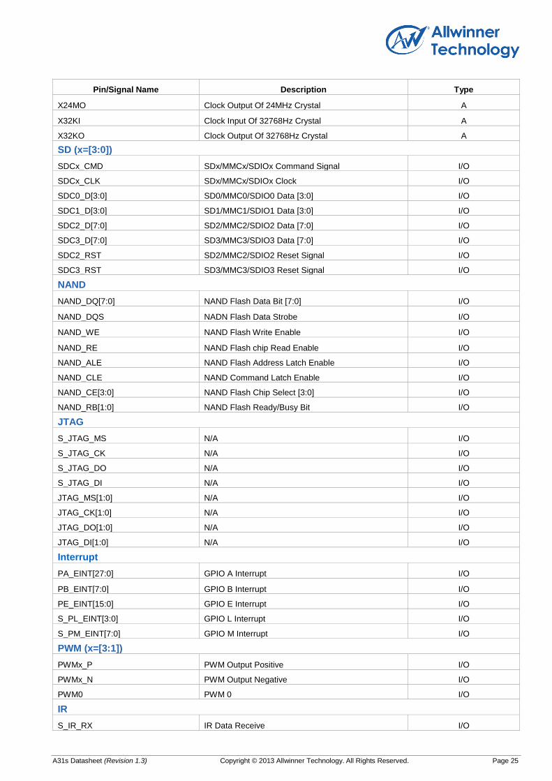
4.3. DETAILED PIN/SIGNAL DESCRIPTION Following table describes A31s pins.
Pin/Signal Name Description Type
DRAM
SDQ[31:0] DRAM DQ[31:0] I/O
SDQS[3:0] DRAM Data Strobe DQS[3:0] I/O
SDQSB[3:0] DRAM DQSB[3:0] I/O
SDQM[3:0] DRAM DQ Mask [3:0] O
SCK DRAM Clock O
SCKB DRAM CKB O
SCKE[1:0] DRAM Clock Enable [1:0] O
SA[15:0] DRAM data Address [15:0] O
SWE DRAM Write Enable O
SCAS DRAM Column Address Strobe O
SRAS DRAM Row Address Strobe O
SCS[1:0] DRAM Chip Select [1:0] O
SBA[2:0] DRAM Bank Address [2:0] O

A31s Datasheet (Revision 1.3) Copyright © 2013 Allwinner Technology. All Rights Reserved. Page 23
Pin/Signal Name Description Type
SODT[1:0] DRAM ODT Control [1:0] O
SRST DRAM Reset O
SZQ DRAM ZQ Calibration A
SVREF DRAM Reference Input P
VCC-DRAM DRAM Power Supply P
VDD-DLL DLL Power Supply P
GPIO
PA[27:0] GPIO A Bit [27:0] I/O
VCC-PA GPIO A Power Supply P
PB[7:0] GPIO B Bit [7:0] I/O
VCC-PB GPIO B Power Supply P
PC[27:0] GPIO C Bit [27:0] I/O
VCC-PC GPIO C Power Supply P
PD[27:0] GPIO D Bit [27:0] I/O
VCC-PD GPIO D Power Supply P
PE[15:0] GPIO E Bit [16:0] I/O
VCC-PE GPIO E Power Supply P
PF[5:0] GPIO F Bit [5:0] I/O
VCC-PF GPIO F Power Supply P
PG[18:0] GPIO G Bit [18:0] I/O
VCC-PG GPIO G Power Supply P
PH[30:0] GPIO H Bit[30:0] I/O
VCC-PH GPIO H Power Supply P
PL[8:0] GPIO L Bit [8:0] I/O
PM[7:0] GPIO M Bit [7:0] I/O
VCC-PM GPIO M Power Supply P
System Control
UBOOT UBOOT I
JTAG_SEL JTAG Mode Select I
BOOT_SEL BOOT Mode Select I
NMI Non-Maskable Interrupt I/O
RESET RESET Signal I
HDMI
HTX0P TMSD Data 0 Positive A
HTX0N TMSD Data 0 Negative A
HTX1P TMSD Data 1 Positive A
HTX1N TMSD Data 1 Negative A
HTX2P TMSD Data 2 Positive A
HTX2N TMSD Data 2 Negative A
HTXCP TMSD Clock Positive A
HTXCN TMSD Clock Negative A
VCC-HDMI HDMI Power Supply P

A31s Datasheet (Revision1.3) Copyright © 2013 Allwinner Technology. All Rights Reserved. Page 24
Pin/Signal Name Description Type
HSCL HDMI DDC Clock A
HSDA HDMI DDC Data A
HHPD HDMI Hot Plug Detection signal A
USB
USB_DM0 USB DM0 Signal A
USB_DP0 USB DP0 Signal A
USB_DM1 USB DM1 Signal A
USB_DP1 USB DP1 Signal A
VCC-USB USB Power Supply P
USB_DM2 USB DM2 Signal A
USB_DP2 USB DP2 Signal A
Audio Codec
PHOUTN Phone Negative Output A
PHOUTP Phone Positive Output A
PHINP Phone Positive Input A
PHINN Phone Negative Input A
HBIAS Headphone Microphone Bias A
MBIAS Master Analog Microphone Bias A
MIC2N MIC Negative Input 2 A
MIC2P MIC Positive Input 2 A
MIC1N MIC Negative Input 1 A
MIC1P MIC Positive Input 1 A
VRA1 Reference (1.5 V) A
VRA2 Reference (1.5 V) A
AVCC Analog Power Supply P
VRP Reference (3.0 V) P
LINEOUTR LINE-OUT Right Channel Output A
LINEOUTL LINE-OUT Left Channel Output A
LINEINR LINE-IN Right Channel Input A
LINEINL LINE-IN Left Channel Input A
AGND Analog Ground G
HPOUTR Headphone Right Channel Output A
HPCOMFB Headphone Common Reference Feedback A
HPCOM Headphone Common Reference A
HPBP Headphone Bypass Output A
VCC-HP Headphone Power Supply A
HPOUTL Headphone Left Channel Output A
LRADC
LRADC0 LRADC Input0 A
Clock
RTC-VIO RTC Power P
VCC-RTC RTC Power Supply P
X24MI Clock Input Of 24MHz Crystal A
A31s Datasheet (Revision 1.3) Copyright © 2013 Allwinner Technology. All Rights Reserved. Page 25
Pin/Signal Name Description Type
X24MO Clock Output Of 24MHz Crystal A
X32KI Clock Input Of 32768Hz Crystal A
X32KO Clock Output Of 32768Hz Crystal A
SD (x=[3:0])
SDCx_CMD SDx/MMCx/SDIOx Command Signal I/O
SDCx_CLK SDx/MMCx/SDIOx Clock I/O
SDC0_D[3:0] SD0/MMC0/SDIO0 Data [3:0] I/O
SDC1_D[3:0] SD1/MMC1/SDIO1 Data [3:0] I/O
SDC2_D[7:0] SD2/MMC2/SDIO2 Data [7:0] I/O
SDC3_D[7:0] SD3/MMC3/SDIO3 Data [7:0] I/O
SDC2_RST SD2/MMC2/SDIO2 Reset Signal I/O
SDC3_RST SD3/MMC3/SDIO3 Reset Signal I/O
NAND
NAND_DQ[7:0] NAND Flash Data Bit [7:0] I/O
NAND_DQS NADN Flash Data Strobe I/O
NAND_WE NAND Flash Write Enable I/O
NAND_RE NAND Flash chip Read Enable I/O
NAND_ALE NAND Flash Address Latch Enable I/O
NAND_CLE NAND Command Latch Enable I/O
NAND_CE[3:0] NAND Flash Chip Select [3:0] I/O
NAND_RB[1:0] NAND Flash Ready/Busy Bit I/O
JTAG
S_JTAG_MS N/A I/O
S_JTAG_CK N/A I/O
S_JTAG_DO N/A I/O
S_JTAG_DI N/A I/O
JTAG_MS[1:0] N/A I/O
JTAG_CK[1:0] N/A I/O
JTAG_DO[1:0] N/A I/O
JTAG_DI[1:0] N/A I/O
Interrupt
PA_EINT[27:0] GPIO A Interrupt I/O
PB_EINT[7:0] GPIO B Interrupt I/O
PE_EINT[15:0] GPIO E Interrupt I/O
S_PL_EINT[3:0] GPIO L Interrupt I/O
S_PM_EINT[7:0] GPIO M Interrupt I/O
PWM (x=[3:1])
PWMx_P PWM Output Positive I/O
PWMx_N PWM Output Negative I/O
PWM0 PWM 0 I/O
IR
S_IR_RX IR Data Receive I/O

A31s Datasheet (Revision1.3) Copyright © 2013 Allwinner Technology. All Rights Reserved. Page 26
Pin/Signal Name Description Type
LCD
LCD_D[23:0] LCD Data Bit [23:0] O
LCD_CLK LCD Clock signal O
LCD_DE LCD Data Enable O
LCD_HSYNC LCD Horizontal SYNC O
LCD_VSYNC LCD Vertical SYNC O
LVDS
LVDS_VP[3:0] LVDS Data Positive Signal Output[3:0] A
LVDS_VN[3:0] LVDS Data Negative Signal Output[3:0] A
LVDS_VPC LVDS Clock Positive Signal Output A
LVDS_VNC LVDS Clock Negative Signal Output A
I2S (x=[1:0])
I2Sx_MCLK I2S Master Clock (system clock) O
I2Sx_BCLK I2S Bit Clock I/O
I2Sx_LRCK I2S Left/Right Channel Select Clock I/O
I2S1_DIN I2S1 Data Input I
I2S1_DOUT I2S1 Data Output O
I2S0_DO[3:0] I2S0 Data Output O
I2S0_DI I2S0 Data Input I
CSI
CSI_PCLK CSI Pixel Clock I
CSI_MCLK CSI Master Clock O
CSI_HSYNC CSI Horizontal SYNC I
CSI_VSYNC CSI Vertical SYNC I
CSI_D[11:0] CSI Data bit [11:0] I
TS
TS_CLK Transport Stream Clock I/O
TS_ERR Transport Stream Error Indicate I/O
TS_SYNC Transport Stream SYNC I/O
TS_DVLD Transport Stream Valid Signal I/O
TS_D[7:0] Transport Stream Data I/O
SPI (x=[3:0])
SPI0_CS0 SPI0 Chip Select signal 0 I/O
SPI1_CS[1:0] SPI1 Chip Select signal[1:0] I/O
SPI2_CS0 SPI2 Chip Select signal 0 I/O
SPI3_CS[1:0] SPI3 Chip Select signal [1:0] I/O
SPIx_CLK SPI Clock signal I/O
SPIx_MOSI SPI Master data Out, Slave data In I/O
SPIx_MISO SPI Master data In, Slave data Out I/O
UART (x=[5:0])
UART1_DTR UART Data Terminal Ready O
UART1_DSR UART Data Set Ready I
UART1_DCD UART Data Carrier Detect I

A31s Datasheet (Revision 1.3) Copyright © 2013 Allwinner Technology. All Rights Reserved. Page 27
Pin/Signal Name Description Type
UART1_RING UART RING indicator I
UARTx_CTS UART Data Clear To Send I
UARTx_RTS UART Data Request To Send O
UARTx_TX[5:0] UART Data Transmit O
UARTx_RX[5:0] UART Data Receive I
S_UART_TX UART Data Transmit O
S_UART_RX UART Data Receive I
TWI (x=[3:0])
TWIx_SCK TWI Serial Clock Signal I/O
TWIx_SDA TWI Serial Data Signal I/O
S_TWI_SCK TWI Serial Clock Signal I/O
S_TWI_SDA TWI Serial Data Signal I/O
S_P2WI_SCK P2WI Serial Clock Signal I/O
S_P2WI_SDA P2WI Serial Data Signal I/O
One Wire
1WIRE One WIRE signal I/O
Clock
CLKA_OUT CLOCK OUT A I/O
CLKB_OUT CLOCK OUT B I/O
CLKC_OUT CLOCK OUT C I/O
CK32KO 32K Crystal Clock Output I/O
RTC_CLKO RTC Clock Output I/O
Table 5-3 Detailed Pin Description
4.4. POWER/GND SIGNAL DESCRIPTION
Note 1) VRP/VRA1/VRA2 are output type, and are not for third party development use.
Signal Name Description Ball#
HDMI
VCC-HDMI HDMI Power Supply U17
USB Power
VCC-USB USB Power Supply T17
IO Power
VCC-PA Power Supply for GPIO A M17,N17
VCC-PB Power Supply for GPIO B D19
VCC-PC Power Supply for GPIO C E8,F8
VCC-PD Power Supply for GPIO D P16,R16,R17
VCC-PE Power Supply for GPIO E E13
VCC-PF Power Supply for GPIO F E7
VCC-PG Power Supply for GPIO G E14

A31s Datasheet (Revision1.3) Copyright © 2013 Allwinner Technology. All Rights Reserved. Page 28
Signal Name Description Ball#
VCC-PH Power Supply for GPIO H F9,F10
VCC-PM Power Supply for GPIO M U18
RTC
VCC_RTC RTC Power Supply V19
DRAM Power
VCC-DRAM DRAM Power Supply P6,R6,T6,T7,U6,U7,U8,V6,V7,W7
VDD-DLL DLL Power Supply U9
Audio Codec
AVCC Analog Power Supply L18
AGND Analog Ground N16
VRP VRP=3.0V, output; K18
VRA1 VRA1=1.5V,output; K19
VRA2 VRA2=1.5V,output; K20
VCC-HP Headphone Power Supply P17
CPU&GPU
VDD-CPU CPU Power Supply F11,F12,F13,F14,F15,F16,G11,G12,G13,G14,G15,G16,G17,H12,H13,H14,H15,H16,H17,J16,J17,K16,K17
VDD-GPU GPU Power Supply J6,J7,K5,K6,K7,L6,L7,M6,M7,N6,N7,P5
System
VDD-SYS System Power Supply T12,T13,T14,T15,T16,U10,U11,U12,U13,U14,U15,U16
VDD-CPUS System Power Supply L16,L17
Ground
GND Ground
W10,G8,H8,H9,H10,H11,J8,J9,J10,J11,J12,J13,J14,J15,K8,K9,K10,K11,K12,K13,K14,K15,L8,L9,L10,L11,L12,L13,L14,L15,M8,M9,M10,M11,M12,M13,M14,M15,M16,N8,N9,N10,N11,N12,N13,N14,N15,P7,P8,P9,P10,P11,P12,P13,P14,P15,R7,R8,R9,R10,R11,R12,R13,R14,R15,T8,T9,T10,T11
Table 5-4 A31s Power/Ground Signal Description

A31s Datasheet (Revision 1.3) Copyright © 2013 Allwinner Technology. All Rights Reserved. Page 29
5 ELECTRICAL CHARACTERISTICS
5.1. ABSOLUTE MAXIMUM RATINGS
Prolonged exposure to absolute maximum ratings (as shown in Table 5-1) may reduce device reliability. Functional operation at these maximum ratings is not implied.
Symbol Parameter Max Unit
II/O In/Out current for input and output / mA
VESD ESD stress voltage HBM(human body mode) / VESD
CDM(charged device mode) N/A N/A
VCC Power supply for I/O 3.6 V
VDD Power supply for Internal Digital Logic 1.32 V
AVCC Power supply for Analog Part 3.0 V
VCC-DRAM Power supply for DRAM Part 2.5 V
VCC-USB Power supply for USB PHY 3.3 V
VDD-DLL Power supply for DLL 1.1 V
VDD-CPU Power supply for CPU 1.32 V
VDD-GPU Power supply for GPU 1.32 V
VCC-HDMI Power supply for HDMI 3.5 V
Tg Storage temperature 125 °C
Table 5-1 Absolute Maximum Ratings
5.2. RECOMMENDED OPERATING CONDITIONS
All A31s modules are strongly recommended to be used under the Operating Conditions given in following Table 5-2.
Symbol Parameter Min Typ Max Unit
Ta Ambient operating temperature (Commercial) -20 / +70 °C
(Extended) N/A N/A N/A °C
VCC Power supply for the IO / 3.0 / V
AVCC Power supply For analog part / 3.0 / V
VCC-DRAM Power supply For DRAMC 1.2 1.5/1.8 2.5 V
VCC-USB Power supply For USB PHY 2.8 3.0 3.3 V
VDD-DLL Power supply For DLL 0.7 1.1 1.32 V
VCC-RTC Power supply For RTCLDO/LOSC/RCOSC 2.8 3.0 3.3 V
VDD-SYS Power supply for VDD_SYS 0.7 1.1 1.32 V
VDD-CPU Power supply for CPU 0.7 1.1 1.32 V

A31s Datasheet (Revision1.3) Copyright © 2013 Allwinner Technology. All Rights Reserved. Page 30
VDD-GPU Power supply for GPU 0.7 1.1 1.32 V
VCC-HDMI Power supply for HDMI 2.8 3.0 3.3 V
GND Ground 0 0 0 V
Table 5-2 Recommended Operating Conditions
5.3. DC ELECTRICAL CHARACTERISTICS
Table 5-3 summarizes the DC electrical characteristics of A31s.
Symbol
Parameter Test Conditions Min Typ Max Unit
VIH High-Level Input Voltage VCC = 3.0V 2.1 3.0 3.6 V
VCC = 1.8V 1.2 1.8 3.6 V
VIL Low-Level Input Voltage VCC = 3.0V -0.3 0 0.7 V
VCC = 1.8V -0.3 0 0.6 V
IIH High-Level Input Current VCC =3.0V, VI = 3.3V / / 10 uA
VCC = 1.8V, VI = 1.8V / / 10 uA
IIL Low-Level Input Current VCC = 3.0V, VI = 0V / / 10 uA
VCC = 1.8V, VI = 0V / / 10 uA
VOH High-Level Output Voltage VCC = 3.0V 2.7 3.0 N/A V
VCC = 1.8V 1.5 1.8 N/A V
VOL Low-Level Output Voltage VCC = 3.0V N/A 0 0.4 V
VCC = 1.8V N/A 0 0.3 V
IOZ Tri-State Output Leakage Current VCC = 3.0V / / 10 uA
VCC = 1.8V / / 10 uA
CIN Input Capacitance - N/A N/A 5 pF
COUT Output Capacitance - N/A N/A 5 pF
Table 5-3 DC Electrical Characteristics
5.4. OSCILLATOR ELECTRICAL CHARACTERISTICS
The A31s clock control module includes 11PLLs, a main oscillator, an on-chip RC oscillator of 466.9KHz ~867.1KHz, and a 32768Hz low power oscillator.
The 24.000MHz frequency is used to generate the main source clock for PLL and the main digital blocks, and the 32768Hz oscillator is used only to provide a low power accurate reference for RTC.
24MHz Oscillator Characteristics
Table 5-4 lists the 24MHz crystal specifications.
Symbol Parameter Min Typ Max Unit
1/(tCPMAIN) Crystal Oscillator Frequency Range - 24.000 - MHz
tST Startup Time – – ms
Frequency Tolerance at 25 °C -40 – +40 ppm
Oscillation Mode Fundamental –

A31s Datasheet (Revision 1.3) Copyright © 2013 Allwinner Technology. All Rights Reserved. Page 31
Maximum change over temperature range -50 – +50 ppm
PON Drive level – – 50 uW
CL Equivalent Load capacitance – – pF
CL1,CL2 Internal Load capacitance(CL1=CL2) – – pF
RS Series Resistance(ESR) – – Ω
Duty Cycle 30 50 70 %
CM Motional capacitance – – pF
CSHUT Shunt capacitance – – pF
RBIAS Internal bias resistor MΩ
Table 5-4 24MHz Oscillator Characteristics
32768Hz Oscillator Characteristics
The 32768Hz crystal is connected between the LOSCI (amplifier input) and LOSCO (amplifier output). Table 5-5 lists the 32768Hz crystal specifications.
Symbol Parameter Min Typ Max Unit
1/(tCPMAIN) Crystal Oscillator Frequency Range 32.768 kHz
tST Startup Time – – ms
Frequency Tolerance at 25 °C -40 – +40 ppm
Oscillation Mode Fundamental –
Maximum change over temperature range -50 – +50 ppm
PON Drive level – – 50 uW
CL Equivalent Load capacitance – – pF
CL1,CL2 Internal Load capacitance(CL1=CL2) – – pF
RS Series Resistance(ESR) – – Ω
Duty Cycle 30 50 70 %
CM Motional capacitance – – pF
CSHUT Shunt capacitance – – pF
RBIAS Internal bias resistor MΩ
Table 5-5 32768Hz Oscillator Characteristics

A31s Datasheet (Revision1.3) Copyright © 2013 Allwinner Technology. All Rights Reserved. Page 32
5.5. POWER UP AND POWER DOWN SEQUENCE
A31s supports four working modes: active mode, idle mode, super standby mode, and power-off mode.
PWRIN delay
PWROK delay
PS
VCC-RTC
VCC-3V3
VDD-CPU
VDD-GPU
VDD-SYS
VCC-DRAM
AVCC
VCC-CPUS
AP-RESET#
PMU-SCK
PMU-SDA
Others Power Supply
PWRON Debounce
Timer
OFF delay
Figure 5-1 A31s Power Up/Down Sequence

A31s Datasheet (Revision 1.3) Copyright © 2013 Allwinner Technology. All Rights Reserved. Page 33
6 PIN ASSIGNMENT
6.1. BALL MAP
1 2 3 4 5 6 7 8 9 10 11 12 13 14 15 16 17 18 19 20 21 22
A NC NC NC
PH11 PH16
PH20 PH24
PE1 PE8
PE13 PG0
PG5 PG14
PB2 PB4 PB6 A
B NC NC NC NC PH10 PH15 PH17 PH21 PH25 PE0 PE3 PE9 PE11 PE14 PG1 PG3 PG10 PG15 PB0 PB3 PB5 PB7 B
C NC PC26 PC27 NC PH9 PH14 PH18 PH22 PH26 NC PE2 PE10 PE12 PE15 PG2 PG4 PG11 PG16 PB1 PA7 PA8 PA9 C
D
NC PC11 PC24 PF0 PH13 PH19 PH27 PH28 NC JTAGSEL1 PE4 PE6 PE7 PG6 PG8 PG12 PG17 VCC-PB PA4 PA13
D
E NC PC10 NC PC15 PC14 PH12 VCC-PF VCC-PC PH23 UBOOT JTAGSEL0 PE5 VCC-PE VCC-PG PG7 PG9 PG13 PG18 PA1 PA14 PA17 PA18 E
F PC4 PC8 PC9 PC12 PC13 NC NC VCC-PC VCC-PH VCC-PH VDD-CPU VDD-CPU VDD-CPU VDD-CPU VDD-CPU VDD-CPU CPU-VDDFB PA0 PA3 PA16 PA19 PA20 F
G
PC0 PC5 PC6 PC7 NC NC GND BOOTSEL1 BOOTSEL0 VDD-CPU VDD-CPU VDD-CPU VDD-CPU VDD-CPU VDD-CPU VDD-CPU PA2 PA12 PA15 PA22
G
H PF4 PF5 PC1 PC2 PC3 PC25 NC GND GND GND GND VDD-CPU VDD-CPU VDD-CPU VDD-CPU VDD-CPU VDD-CPU PA5 PA11 PA21 PA23 PA26 H
J SDQ2 SDQ6 PF1 PF2 PF3 VDD-GPU VDD-GPU GND GND GND GND GND GND GND GND VDD-CPU VDD-CPU PA6 PA10 PA25 PA24 PA27 J
K
SDQ4 SDQ0 SZQ VDD-GPU VDD-GPU VDD-GPU GND GND GND GND GND GND GND GND VDD-CPU VDD-CPU VRP VRA1 VRA2 HPOUTR
K
L SDQS0 SDQS0B SDQ5 SDQM0 SRAS VDD-GPU VDD-GPU GND GND GND GND GND GND GND GND VDD-CPUS VDD-CPUS AVCC HPOUTL MIC1P PHINP PHINN L
M SDQ7 SDQ3 SDQ1 SODT SODT1 VDD-GPU VDD-GPU GND GND GND GND GND GND GND GND GND VCC-PA HPCOMFB LINEINL MIC1N MIC2P MIC2N M
N
SDQ14 SDQ10 SCS1 SCAS VDD-GPU VDD-GPU GND GND GND GND GND GND GND GND AGND VCC-PA HPCOM LINEINR MBIAS HPBP
N
P SDQ12 SDQ8 SDQ13 SDQM1 VDD-GPU VCC-DRAM GND GND GND GND GND GND GND GND GND VCC-PD VCC-HP PHOUTN PHOUTP HBIAS LINEOUTR LINEOUTL P
R SDQS1 SDQS1B SDQ11 SCS SA2 VCC-DRAM GND GND GND GND GND GND GND GND GND VCC-PD VCC-PD PM1 PM0 PM2 PM4 LRADC0 R
T
SDQ15 SA3 SBA2 SCKE VCC-DRAM VCC-DRAM GND GND GND GND VDD-SYS VDD-SYS VDD-SYS VDD-SYS VDD-SYS VCC-USB PM3 PM6 PM5 PM7
T
U SDQ9 SBA0 SA0 SRST SA10 VCC-DRAM VCC-DRAM VCC-DRAM VDD-DLL VDD-SYS VDD-SYS VDD-SYS VDD-SYS VDD-SYS VDD-SYS VDD-SYS VCC-HDMI VCC-PM PL5 PL3 PL0 RESET U
V SWE SA5 SCK SA15 SBA1 VCC-DRAM VCC-DRAM SA8 SA6 SA11 PD27 PD25 PD23 PD9 PD7 PD5 PD3 PD1 VCC-RTC PL8 X32KO X32KI V
W
SA7 SCKB SA1 SVREF SA12 VCC-DRAM SA14 SA4 GND PD26 PD24 PD22 PD8 PD6 PD4 PD2 PD0 NMI PL7 PL2
W
Y SA9 SA13 SCKE1 SDQM2 SDQ17 SDQ30 SDQ26 SDQS3B SDQ31 X24MO HHPD HTX1N HSDA HTX2N PD20 PD19 PD21 PD10 PL6 PL4 DM0 DP0 Y
AA SDQ22 SDQ20 SDQS2 SDQ23 SDQ19 SDQ28 SDQS3 SDQ29 SDQ27 X24MI HTXCN HTX0P HTX1P HTX2P PD16 PD18 PD15 PD13 PD11 VIO-RTC DM1 DP1 AA
AB SDQ18 SDQ16 SDQS2B
SDQ21 SDQ24
SDQ25 SDQM3
HTXCP HTX0N
HSCL PD17
PD14 PD12
PL1 DM2 DP2 AB
1 2 3 4 5 6 7 8 9 10 11 12 13 14 15 16 17 18 19 20 21 22

A31s Datasheet (Revision 1.3) Copyright © 2013 Allwinner Technology. All Rights Reserved. Page 34
6.2. PIN DIMENSION